JP7345382B2 - Plasma processing equipment and control method - Google Patents
Plasma processing equipment and control method Download PDFInfo
- Publication number
- JP7345382B2 JP7345382B2 JP2019224853A JP2019224853A JP7345382B2 JP 7345382 B2 JP7345382 B2 JP 7345382B2 JP 2019224853 A JP2019224853 A JP 2019224853A JP 2019224853 A JP2019224853 A JP 2019224853A JP 7345382 B2 JP7345382 B2 JP 7345382B2
- Authority
- JP
- Japan
- Prior art keywords
- voltage
- state
- electrode
- plasma
- potential
- Prior art date
- Legal status (The legal status is an assumption and is not a legal conclusion. Google has not performed a legal analysis and makes no representation as to the accuracy of the status listed.)
- Active
Links
Images


Classifications
-
- H—ELECTRICITY
- H01—ELECTRIC ELEMENTS
- H01J—ELECTRIC DISCHARGE TUBES OR DISCHARGE LAMPS
- H01J37/00—Discharge tubes with provision for introducing objects or material to be exposed to the discharge, e.g. for the purpose of examination or processing thereof
- H01J37/32—Gas-filled discharge tubes
- H01J37/32009—Arrangements for generation of plasma specially adapted for examination or treatment of objects, e.g. plasma sources
- H01J37/32082—Radio frequency generated discharge
- H01J37/32174—Circuits specially adapted for controlling the RF discharge
-
- H—ELECTRICITY
- H01—ELECTRIC ELEMENTS
- H01J—ELECTRIC DISCHARGE TUBES OR DISCHARGE LAMPS
- H01J37/00—Discharge tubes with provision for introducing objects or material to be exposed to the discharge, e.g. for the purpose of examination or processing thereof
- H01J37/32—Gas-filled discharge tubes
- H01J37/32009—Arrangements for generation of plasma specially adapted for examination or treatment of objects, e.g. plasma sources
- H01J37/32082—Radio frequency generated discharge
- H01J37/32137—Radio frequency generated discharge controlling of the discharge by modulation of energy
- H01J37/32146—Amplitude modulation, includes pulsing
-
- H—ELECTRICITY
- H01—ELECTRIC ELEMENTS
- H01J—ELECTRIC DISCHARGE TUBES OR DISCHARGE LAMPS
- H01J37/00—Discharge tubes with provision for introducing objects or material to be exposed to the discharge, e.g. for the purpose of examination or processing thereof
- H01J37/32—Gas-filled discharge tubes
- H01J37/32009—Arrangements for generation of plasma specially adapted for examination or treatment of objects, e.g. plasma sources
- H01J37/32082—Radio frequency generated discharge
- H01J37/32174—Circuits specially adapted for controlling the RF discharge
- H01J37/32183—Matching circuits
-
- H—ELECTRICITY
- H01—ELECTRIC ELEMENTS
- H01J—ELECTRIC DISCHARGE TUBES OR DISCHARGE LAMPS
- H01J37/00—Discharge tubes with provision for introducing objects or material to be exposed to the discharge, e.g. for the purpose of examination or processing thereof
- H01J37/32—Gas-filled discharge tubes
- H01J37/32431—Constructional details of the reactor
- H01J37/32532—Electrodes
-
- H—ELECTRICITY
- H01—ELECTRIC ELEMENTS
- H01J—ELECTRIC DISCHARGE TUBES OR DISCHARGE LAMPS
- H01J37/00—Discharge tubes with provision for introducing objects or material to be exposed to the discharge, e.g. for the purpose of examination or processing thereof
- H01J37/32—Gas-filled discharge tubes
- H01J37/32431—Constructional details of the reactor
- H01J37/32623—Mechanical discharge control means
-
- H—ELECTRICITY
- H01—ELECTRIC ELEMENTS
- H01J—ELECTRIC DISCHARGE TUBES OR DISCHARGE LAMPS
- H01J37/00—Discharge tubes with provision for introducing objects or material to be exposed to the discharge, e.g. for the purpose of examination or processing thereof
- H01J37/32—Gas-filled discharge tubes
- H01J37/32431—Constructional details of the reactor
- H01J37/32715—Workpiece holder
- H01J37/32724—Temperature
-
- H—ELECTRICITY
- H01—ELECTRIC ELEMENTS
- H01J—ELECTRIC DISCHARGE TUBES OR DISCHARGE LAMPS
- H01J2237/00—Discharge tubes exposing object to beam, e.g. for analysis treatment, etching, imaging
- H01J2237/002—Cooling arrangements
-
- H—ELECTRICITY
- H01—ELECTRIC ELEMENTS
- H01J—ELECTRIC DISCHARGE TUBES OR DISCHARGE LAMPS
- H01J2237/00—Discharge tubes exposing object to beam, e.g. for analysis treatment, etching, imaging
- H01J2237/32—Processing objects by plasma generation
- H01J2237/33—Processing objects by plasma generation characterised by the type of processing
- H01J2237/334—Etching
-
- H—ELECTRICITY
- H01—ELECTRIC ELEMENTS
- H01J—ELECTRIC DISCHARGE TUBES OR DISCHARGE LAMPS
- H01J37/00—Discharge tubes with provision for introducing objects or material to be exposed to the discharge, e.g. for the purpose of examination or processing thereof
- H01J37/32—Gas-filled discharge tubes
- H01J37/32431—Constructional details of the reactor
- H01J37/32458—Vessel
- H01J37/32467—Material
-
- H—ELECTRICITY
- H01—ELECTRIC ELEMENTS
- H01J—ELECTRIC DISCHARGE TUBES OR DISCHARGE LAMPS
- H01J37/00—Discharge tubes with provision for introducing objects or material to be exposed to the discharge, e.g. for the purpose of examination or processing thereof
- H01J37/32—Gas-filled discharge tubes
- H01J37/32431—Constructional details of the reactor
- H01J37/32623—Mechanical discharge control means
- H01J37/32633—Baffles
-
- H—ELECTRICITY
- H01—ELECTRIC ELEMENTS
- H01J—ELECTRIC DISCHARGE TUBES OR DISCHARGE LAMPS
- H01J37/00—Discharge tubes with provision for introducing objects or material to be exposed to the discharge, e.g. for the purpose of examination or processing thereof
- H01J37/32—Gas-filled discharge tubes
- H01J37/32431—Constructional details of the reactor
- H01J37/32623—Mechanical discharge control means
- H01J37/32642—Focus rings
-
- H—ELECTRICITY
- H01—ELECTRIC ELEMENTS
- H01J—ELECTRIC DISCHARGE TUBES OR DISCHARGE LAMPS
- H01J37/00—Discharge tubes with provision for introducing objects or material to be exposed to the discharge, e.g. for the purpose of examination or processing thereof
- H01J37/32—Gas-filled discharge tubes
- H01J37/32431—Constructional details of the reactor
- H01J37/32623—Mechanical discharge control means
- H01J37/32651—Shields, e.g. dark space shields, Faraday shields
-
- H—ELECTRICITY
- H01—ELECTRIC ELEMENTS
- H01L—SEMICONDUCTOR DEVICES NOT COVERED BY CLASS H10
- H01L21/00—Processes or apparatus adapted for the manufacture or treatment of semiconductor or solid state devices or of parts thereof
- H01L21/67—Apparatus specially adapted for handling semiconductor or electric solid state devices during manufacture or treatment thereof; Apparatus specially adapted for handling wafers during manufacture or treatment of semiconductor or electric solid state devices or components ; Apparatus not specifically provided for elsewhere
- H01L21/67005—Apparatus not specifically provided for elsewhere
- H01L21/67011—Apparatus for manufacture or treatment
- H01L21/67017—Apparatus for fluid treatment
- H01L21/67063—Apparatus for fluid treatment for etching
- H01L21/67069—Apparatus for fluid treatment for etching for drying etching
-
- H—ELECTRICITY
- H01—ELECTRIC ELEMENTS
- H01L—SEMICONDUCTOR DEVICES NOT COVERED BY CLASS H10
- H01L21/00—Processes or apparatus adapted for the manufacture or treatment of semiconductor or solid state devices or of parts thereof
- H01L21/67—Apparatus specially adapted for handling semiconductor or electric solid state devices during manufacture or treatment thereof; Apparatus specially adapted for handling wafers during manufacture or treatment of semiconductor or electric solid state devices or components ; Apparatus not specifically provided for elsewhere
- H01L21/683—Apparatus specially adapted for handling semiconductor or electric solid state devices during manufacture or treatment thereof; Apparatus specially adapted for handling wafers during manufacture or treatment of semiconductor or electric solid state devices or components ; Apparatus not specifically provided for elsewhere for supporting or gripping
- H01L21/6831—Apparatus specially adapted for handling semiconductor or electric solid state devices during manufacture or treatment thereof; Apparatus specially adapted for handling wafers during manufacture or treatment of semiconductor or electric solid state devices or components ; Apparatus not specifically provided for elsewhere for supporting or gripping using electrostatic chucks
- H01L21/6833—Details of electrostatic chucks
Landscapes
- Physics & Mathematics (AREA)
- Engineering & Computer Science (AREA)
- Plasma & Fusion (AREA)
- Chemical & Material Sciences (AREA)
- Analytical Chemistry (AREA)
- Plasma Technology (AREA)
- Drying Of Semiconductors (AREA)
Description
本開示は、プラズマ処理装置及び制御方法に関する。 The present disclosure relates to a plasma processing apparatus and a control method.
例えば、特許文献1は、プラズマの状態によらず、プラズマの均一性を容易に確保することができるプラズマ処理装置を提供することを提案している。
For example,
プラズマ処理装置の処理容器内に配置されたパーツであって、プラズマに暴露されるパーツがスパッタされることがある。 Parts placed in a processing chamber of a plasma processing apparatus and exposed to plasma may be sputtered.
本開示は、イオンの衝突エネルギーを制御することができる技術を提供する。 The present disclosure provides techniques that can control the collision energy of ions.
本開示の一の態様によれば、処理容器と、前記処理容器内で被処理体を載置する電極と、前記処理容器内にプラズマを供給するプラズマ生成源と、前記電極に所望の波形のバイアスパワーを供給するバイアス電源と、前記処理容器内のプラズマに暴露されるパーツと、前記パーツに所望の波形の電圧を供給する電源と、前記電圧が、第1の電圧値を有する第1の状態と、前記第1の電圧値よりも高い第2の電圧値を有する第2の状態とを周期的に繰り返し、前記電極の電位の各周期内の部分期間に前記第1の電圧値を印加し、前記第1の状態と前記第2の状態とが連続するように前記第2の電圧値を印加する第1制御手順を含むプログラムを有する記憶媒体と、前記記憶媒体のプログラムを実行する制御部と、を有するプラズマ処理装置が提供される。 According to one aspect of the present disclosure, a processing container, an electrode on which an object to be processed is placed in the processing container, a plasma generation source that supplies plasma into the processing container, and a plasma generating source configured to generate a desired waveform in the electrode. a bias power supply for supplying bias power; a part exposed to plasma in the processing container; a power supply supplying a voltage of a desired waveform to the part; and a second state having a second voltage value higher than the first voltage value are periodically repeated, and the first voltage value is applied during a partial period within each period of the potential of the electrode. a storage medium having a program including a first control procedure for applying the second voltage value so that the first state and the second state are continuous; and a control for executing the program in the storage medium. There is provided a plasma processing apparatus having:
一の側面によれば、イオンの衝突エネルギーを制御することができる。 According to one aspect, the collision energy of ions can be controlled.
以下、本開示を実施するための形態について図面を参照して説明する。なお、本明細書及び図面において、実質的に同一の構成については、同一の符号を付することにより重複した説明を省く。 Hereinafter, embodiments for implementing the present disclosure will be described with reference to the drawings. Note that, in this specification and the drawings, substantially the same configurations are given the same reference numerals to omit redundant explanation.
[はじめに]
プラズマ処理装置において、高周波電力を印加する電極の電位が処理容器の壁や処理容器内のその他のパーツの電位を上回ると、前記壁やパーツがスパッタされる現象が発生し、プロセスの結果に影響を与える。また、ウエハWに対するプラズマ処理では、プラズマ処理中に生成された副生成物が処理容器の側壁や天井壁に付着する。この場合、副生成物を除去するクリーニング処理が必要となり生産性が低下する。
[Introduction]
In plasma processing equipment, if the potential of the electrode that applies high-frequency power exceeds the potential of the walls of the processing vessel or other parts within the processing vessel, a phenomenon occurs in which the walls and parts are sputtered, which affects the process results. give. Furthermore, in the plasma processing of the wafer W, byproducts generated during the plasma processing adhere to the side walls and ceiling wall of the processing container. In this case, cleaning treatment to remove by-products is required, resulting in decreased productivity.
そこで、従来から処理容器内の電極に対して処理容器の壁への単位面積当たりのイオンの衝突エネルギーを低く見せることが行われている。また、処理容器の側壁にコーティングする溶射膜の厚さを変更したり、側壁のコーティングに使用する材料を結合力のより強い材質へ変更したりすることで、イオンの衝突エネルギーにより壁がスパッタされることを抑制することが行われている。さらに、ウエハレスドライクリーニング(WLDC)の手順を示したレシピの、クリーニング時間や供給電力等の設定を、処理容器内のコンディションに応じて調整することが行われている。 Therefore, conventional techniques have been used to make the collision energy of ions per unit area with respect to the walls of the processing container appear lower than the electrodes within the processing container. In addition, by changing the thickness of the sprayed film that coats the side walls of the processing container or by changing the material used to coat the side walls to a material with stronger bonding strength, it is possible to prevent the walls from sputtering due to ion collision energy. Efforts are being made to suppress this. Further, settings such as cleaning time and power supply in a recipe indicating a waferless dry cleaning (WLDC) procedure are adjusted in accordance with the conditions inside the processing container.
以下に説明する一実施形態にかかるプラズマ処理装置では、高周波電力を印加する電極電位の変動に追従して、処理容器内のプラズマに暴露され、かつ副生成物が付着するパーツに任意の直流電圧を印加する。これにより、当該パーツへのイオンの衝突エネルギーを制御し、当該パーツへのスパッタの低減を図る。また、クリーニング処理の効率化を実現する。処理容器内のプラズマに暴露され、かつ副生成物が付着するパーツは、処理容器内パーツにより構成される。当該パーツは、天井壁、インシュレータリング、デポシールド、及びバッフル板等の処理容器内のパーツの少なくともいずれかであってもよい。又は、当該パーツは、上部電極の下方に形成された処理空間、ガス空間或いはエッジリングの上空外側に配置した専用のパーツの少なくともいずれかであってもよい。ただし、ウォールスパッタ抑制効果のある場合には、当該パーツは、処理容器内のプラズマに暴露されるパーツであって、副生成物が付着していないパーツであってもよい。以下では、プラズマの影響下にある前記パーツの一例として、デポシールドを例にあげてプラズマ処理装置について説明する。 In a plasma processing apparatus according to an embodiment described below, an arbitrary DC voltage is applied to parts exposed to plasma in a processing container and to which byproducts are attached, following fluctuations in electrode potential to which high-frequency power is applied. Apply. This controls the impact energy of ions on the part and reduces spatter on the part. It also makes the cleaning process more efficient. Parts inside the processing container that are exposed to plasma and to which by-products are attached are constituted by parts inside the processing container. The part may be at least one of parts inside the processing container, such as a ceiling wall, an insulator ring, a deposit shield, and a baffle plate. Alternatively, the part may be at least one of a processing space formed below the upper electrode, a gas space, or a dedicated part disposed above and outside the edge ring. However, if there is an effect of suppressing wall spatter, the part may be a part that is exposed to plasma in the processing container and has no by-products attached thereto. In the following, a plasma processing apparatus will be described using a deposit shield as an example of the parts that are under the influence of plasma.
以下、ソースパワーとしての高周波をHFともいい、ソースパワーをHF電力ともいう。また、ソースパワーの周波数よりも低い周波数のバイアスパワーとしての高周波をLFともいい、バイアスパワーをLF電力ともいう。 Hereinafter, the high frequency as the source power will also be referred to as HF, and the source power will also be referred to as HF power. Further, a high frequency as a bias power having a frequency lower than the frequency of the source power is also referred to as LF, and the bias power is also referred to as LF power.
[プラズマ処理装置の全体構成]
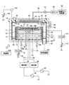
図1Aは、一実施形態に係るプラズマ処理装置1の一例を示す図である。本実施形態にかかるプラズマ処理装置1は、容量結合型の平行平板プラズマ処理装置であり、例えば表面が陽極酸化処理されたアルミニウムや溶射された酸化イットリウム(Y2O3)からなる円筒状の処理容器10を有している。処理容器10は接地されている。
[Overall configuration of plasma processing equipment]
FIG. 1A is a diagram showing an example of a
処理容器10の底部には、セラミックス等からなる絶縁板12を介して円柱状の支持台14が配置され、この支持台14の上に例えばアルミニウムからなる載置台16が設けられている。載置台16は下部電極を構成し、その上に被処理体の一例であるウエハWが載置される。
A
載置台16の上面には、ウエハWを静電力で吸着保持する静電チャック20が設けられている。静電チャック20は、導電膜からなる電極20aを絶縁層20bで挟んだ構造を有し、電極20aには直流電源22が接続されている。そして、直流電源22からの直流電圧により生じたクーロン力等の静電力によりウエハWが静電チャック20に吸着保持される。
An
載置台16上であってウエハWの周縁には、例えばシリコンからなる導電性のエッジリング24が配置されている。載置台16および支持台14の外周側面には、例えば石英からなる円筒状の内壁部材26が設けられている。エッジリング24の外周側面にはインシュレータリング25が設けられている。
On the mounting table 16 and around the periphery of the wafer W, a
支持台14の内部には、例えば円周上に冷媒室28が設けられている。冷媒室28には、外部に設けられたチラーユニットより配管30a,30bを介して所定温度の冷媒、例えば冷却水が循環供給され、冷媒の温度によって載置台16上のウエハWの処理温度が制御される。さらに、伝熱ガス供給機構からの伝熱ガス、例えばHeガスがガス供給ライン32を介して静電チャック20の上面とウエハWの裏面との間に供給される。
A
載置台16の上方には、載置台16と対向して上部電極34が設けられている。上部電極34と下部電極間の間はプラズマ処理空間となる。上部電極34は、載置台16上のウエハWと対向してプラズマ処理空間と接する面、つまり対向面を形成する。
An
上部電極34は、絶縁性の遮蔽部材42を介して、処理容器10の上部に支持されている。上部電極34は、載置台16との対向面を構成しかつ多数のガス吐出孔37を有する電極板36と、この電極板36を着脱自在に支持し、導電性材料、例えば表面が陽極酸化処理されたアルミニウムからなる電極支持体38とを有する。電極板36は、シリコンやSiCで構成されるのが好ましい。電極支持体38の内部には、ガス拡散室40が設けられ、このガス拡散室40からはガス吐出孔37に連通する多数のガス通流孔41が下方に延びている。
The
電極支持体38には、ガス拡散室40へ処理ガスを導くガス導入口62が形成されており、このガス導入口62にはガス供給管64が接続され、ガス供給管64には処理ガス供給源66が接続されている。ガス供給管64には、上流側から順にマスフローコントローラ(MFC)68および開閉バルブ70が設けられている。そして、処理ガス供給源66から、エッチングのための処理ガスがガス供給管64からガス拡散室40に至り、ガス通流孔41を介しガス吐出孔37からシャワー状にプラズマ処理空間に吐出される。このようにして上部電極34は処理ガスを供給するためのシャワーヘッドとして機能する。
The
エッジリング24には、可変直流電源50が電気的に接続され、可変直流電源50から直流電圧が印加される。可変直流電源50から供給される直流電圧及び直流電流の極性及び電流・電圧と、これらをオン・オフする電子スイッチの制御は、制御部200により行われる。可変直流電源50には、LF及びHFの電流をカットし、可変直流電源50を保護するローパスフィルタ51が接続されている。
A variable
デポシールド11には、可変直流電源115が電気的に接続され、可変直流電源115から直流電圧が印加される。可変直流電源115から供給される直流電圧及び直流電流の極性、及び直流電圧及び直流電流とこれらをオン・オフする電子スイッチの制御は、制御部200により行われる。可変直流電源115には、LF及びHFの電流をカットし、可変直流電源115を保護するローパスフィルタ116が接続されている。本実施形態では、可変直流電源115はデポシールド11に接続されているが、これに限られず、処理容器10内のパーツ、例えば処理容器10の天井壁、インシュレータリング25及びバッフル板83の少なくともいずれかのパーツに接続されてもよい。更に、可変直流電源115は、載置台16と対向する上部電極34の下方に設けられた処理空間若しくはガス空間、又はエッジリング24の上空外側に配置した専用のパーツに接続されてもよい。また、可変直流電源115は、一つに限られず、二つ以上がデポシールド11や天井壁等の少なくともいずれかのパーツに接続されてもよい。図1には、一例として、エッジリング24の上方の外側に専用のパーツ101が配置されている。パーツ101は内部に電極を有し、可変直流電源104が電気的に接続され、可変直流電源104からその電極に直流電圧が印加される。可変直流電源104には、LF及びHFの電流をカットし、また、可変直流電源104を保護するローパスフィルタ103が接続されている。パーツ101は、リング状であってもよいし、円弧状であってもよいし、その他の形状であってもよい。パーツ101は、例えば、シリコン(Si)やシリコンカーバイト(SiC)から構成される。
A variable
載置台16には、給電棒47及び整合器46を介して第1の高周波電源48が接続されている。第1の高周波電源48は、載置台16にLF電力を印加する。これにより、載置台16上のウエハWにイオンが引き込まれる。第1の高周波電源48は、200kHz~13.56MHzの範囲内の周波数の高周波電力を出力する。整合器46は第1の高周波電源48の内部インピーダンスと負荷インピーダンスとを整合させる。
A first high
載置台16には、給電棒89及び整合器88を介して第2の高周波電源90が接続されている。第2の高周波電源90は、載置台16にHF電力を印加する。HFの周波数は、13.56MHz以上、例えば100MHzであってもよい。LFの周波数はHFの周波数よりも低く、例えば400kHzであってもよい。整合器88は、第2の高周波電源90の内部インピーダンスと負荷インピーダンスとを整合させる。載置台16には、所定の高周波をグランドに通すためのフィルタが接続されてもよい。なお、第2の高周波電源90から供給されるHF電力を、上部電極34に印加してもよい。
A second high
処理容器10の底部には排気口80が設けられ、この排気口80に排気管82を介して排気装置84が接続されている。排気装置84は、ターボ分子ポンプなどの真空ポンプを有しており、処理容器10内を所望の真空度まで減圧可能となる。また、処理容器10の側壁にはウエハWの搬入出口85が設けられており、この搬入出口85はゲートバルブ86により開閉可能である。また、処理容器10の内壁に沿ってエッチング時に生成された副生成物(デポ)が付着することを防止するためのデポシールド11が着脱自在に設けられている。すなわち、デポシールド11が処理容器の壁部を構成している。また、デポシールド11は、内壁部材26の外周にも設けられている。処理容器10の底部の処理容器壁側のデポシールド11と内壁部材26側のデポシールド11との間にはバッフル板83が設けられている。デポシールド11およびバッフル板83としては、アルミニウム材にY2O3等のセラミックスを被覆したものを用いることができる。
An exhaust port 80 is provided at the bottom of the
かかる構成のプラズマ処理装置においてエッチング処理を行う際には、まず、ゲートバルブ86を開状態とし、搬入出口85を介してエッチング対象であるウエハWを処理容器10内に搬入し、載置台16上に載置する。そして、処理ガス供給源66からエッチングのための処理ガスを所定の流量でガス拡散室40へ供給し、ガス通流孔41およびガス吐出孔37を介して処理容器10内へ供給する。また、排気装置84により処理容器10内を排気し、その中の圧力を例えば0.1~150Paの範囲内の設定値とする。ここで、処理ガスとしては、従来用いられている種々のものを採用することができ、例えばC4F8ガスのようなフルオロカーボンガス(CxFy)に代表されるハロゲン元素を含有するガスを好適に用いることができる。さらに、ArガスやO2ガス等の他のガスが含まれていてもよい。
When performing an etching process in the plasma processing apparatus having such a configuration, first, the
このように処理容器10内にエッチングガスを導入した状態で、第2の高周波電源90からHF電力を載置台16に印加する。また、第1の高周波電源48からLF電力を載置台16に印加する。また、直流電源22から直流電圧を電極20aに印加し、ウエハWを載置台16に保持する。また、可変直流電源50から直流電圧をエッジリング24に印加する。
With the etching gas introduced into the
上部電極34のガス吐出孔37から吐出された処理ガスは、主にHF電力により解離及び電離しプラズマが生成される。プラズマ中のラジカルやイオンによってウエハWの被処理面がエッチングされる。また、載置台16にLF電力を印加することで、プラズマ中のイオンを制御し、高アスペクト比のホールのエッチングを可能とする等、プラズマの制御マージンを広くできる。
The processing gas discharged from the
プラズマ処理装置1には、装置全体の動作を制御する制御部200が設けられている。制御部200は、ROM(Read Only Memory)及びRAM(Random Access Memory)等のメモリに格納されたプロセスレシピに従って、エッチング等の所望のプラズマ処理を実行する。プロセスレシピには、プロセス条件に対する装置の制御情報であるプロセス時間、圧力(ガスの排気)、高周波電力や電圧、各種ガス流量が設定されてもよい。また、プロセスレシピには、処理容器内温度(上部電極温度、処理容器の側壁温度、ウエハW温度、静電チャック温度等)、チラーから出力される冷媒の温度などが設定されてもよい。なお、これらのプログラムや処理条件を示すプロセスレシピは、ハードディスクや半導体メモリに記憶されてもよい。また、プロセスレシピは、CD-ROM、DVD等の可搬性のコンピュータにより読み取り可能な記憶媒体に収容された状態で所定位置にセットされ、読み出されるようにしてもよい。
The
例えば、制御部200は、可変直流電源115から出力する直流電圧(直流電圧)を、バイアスパワーの伝達経路で測定される、電圧、電流、電磁界、発生したプラズマの発光周期又はウエハW(下部電極)上のプラズマのシース厚の変化(以下、「周期的に変動するパラメータ」ともいう。)の各周期内の部分期間に印加し、直流電圧のオンとオフやその電圧の大小を交互に繰り返すように制御してもよい。制御部200は、バイアスパワーの高周波の周期若しくはバイアスパワーのパルス波(以下、「DCパルス」ともいう。)の周期に同期する信号により、直流電圧のオンとオフやその電圧の大小を交互に繰り返すように制御してもよい。
For example, the
バイアスパワーの供給経路とは、第1の高周波電源48→整合器46→給電棒47→載置台16→プラズマ→上部電極34→(グランド)をいう。バイアスパワーの伝達経路で測定される電圧、電流、電磁界とは、第1の高周波電源48から整合器46の内部及び給電棒47を介して載置台16に至るまでのパーツと上部電極34で測定される電圧、電流、電磁界、又は、プラズマで測定される電磁界をいう。
The bias power supply path is first high
直流電圧は、後述する第1の状態と第2の状態とを周期的に繰り返し、第1の状態は、周期的に変動するパラメータの各周期内の部分期間に第1の電圧値を印加し、第2の状態は、第1の状態と連続して第2の電圧値を印加するように制御される。直流電圧が、第1の状態と、第2の状態と、2つ以上の電圧値を有する2以上の状態とを周期的に繰り返し、パラメータの各周期内の部分期間に第1の電圧値を印加し、第1の状態と第2の状態と2以上の状態とが連続するように第2の電圧値と2つ以上の電圧値とを順に印加してもよい。「周期的に変動するパラメータ」は、周期的に変動する電極電位の一例である。 The DC voltage periodically repeats a first state and a second state, which will be described later. , the second state is controlled to apply the second voltage value continuously with the first state. The DC voltage periodically repeats a first state, a second state, and two or more states having two or more voltage values, and the first voltage value is set in a partial period within each period of the parameter. The second voltage value and two or more voltage values may be sequentially applied so that the first state, the second state, and two or more states are continuous. A "periodically varying parameter" is an example of a periodically varying electrode potential.
周期的に変動するパラメータは、載置台16から給電棒47を介して接続される整合器の内部までのいずれかの部材において測定される電圧、電流又は電磁界のいずれかであることが好ましい。
It is preferable that the periodically varying parameter is a voltage, a current, or an electromagnetic field measured in any member from the mounting table 16 to the inside of the matching box connected via the
バイアスパワーの伝達経路で周期的に変動するパラメータを測定する方法としては、バイアスパワーの伝達経路のいずれかのパーツの近傍に電圧センサ、電流センサ又はBZセンサ(誘導磁場を測るセンサ)を設置することで各パーツの電圧、電流又は誘導磁場を計測する方法が一例として挙げられる。なお、図2には、電圧センサ300を示したが、これに限られず、電流センサ又はBZセンサであってもよい。また、上記各センサの配置は、給電棒47に接続されることが好ましいが、これに限られない。電圧センサ300等のセンサからの信号は、例えば制御部200の信号発生回路102に入力される。
A method for measuring periodically changing parameters in the bias power transmission path is to install a voltage sensor, current sensor, or BZ sensor (a sensor that measures the induced magnetic field) near any part of the bias power transmission path. An example is a method of measuring the voltage, current, or induced magnetic field of each part. Although the
更に、プラズマの発光周期、ウエハW上のプラズマのシース厚の変化の周期を指標にしても良い。プラズマの発光周期は、フォトダイオード、フォトマイクロセンサ、フォトマルチプライヤー等の光電変換素子で検出できる。シース厚については、ICCDカメラなどを用いてナノsecの間隔(例えば10~250nsec)でシャッターを切り、これにより、シース厚の変化を測定できる。例えば、可変直流電源115から出力する直流電圧をLFの電圧の周期に同期させるように制御してもよい。これにより、イオンの衝突エネルギーを制御することができる。また、クリーニング処理の効率化を図ることができる。
Furthermore, the light emission period of the plasma or the period of change in the sheath thickness of the plasma on the wafer W may be used as an index. The emission period of plasma can be detected by a photoelectric conversion element such as a photodiode, a photomicrosensor, or a photomultiplier. Regarding the sheath thickness, changes in the sheath thickness can be measured by using an ICCD camera or the like and shuttering at nanosec intervals (for example, 10 to 250 nsec). For example, the DC voltage output from the variable
なお、載置台16は、ウエハWを載置する電極(第1の電極)の一例である。上部電極は、載置台16と対向する電極(第2の電極)の一例である。第1の高周波電源48は、載置台16にLF電力(バイアスパワー)を供給するバイアス電源の一例である。第2の高周波電源90は、載置台16又は上部電極34にLF電力よりも高い周波数のソースパワーを供給するソース電源の一例である。可変直流電源115は、処理容器10内のプラズマに暴露されるパーツに電圧を供給する電源の一例である。可変直流電源115は、直流電源であってもよい。制御部200は、バイアス電源、ソース電源及び直流電源を制御する制御部の一例である。バイアスパワーを印加する下部電極(載置台16)の電位を、電極電位ともいう。
Note that the mounting table 16 is an example of an electrode (first electrode) on which the wafer W is mounted. The upper electrode is an example of an electrode (second electrode) facing the mounting table 16. The first high-
なお、図1のプラズマ処理装置1では、デポシールド11に可変直流電源115が電気的に接続され、可変直流電源115から直流電圧が印加されたが、これに限られない。可変直流電源115が、処理容器10内のパーツ、例えば処理容器10の天井壁、インシュレータリング25及びバッフル板83の少なくともいずれかのパーツに接続され、これらのパーツの少なくともいずれかに直流電圧を印加してもよい。更に、可変直流電源115が、載置台16と対向する上部電極34の下方に設けられた処理空間若しくはガス空間、又はエッジリング24の上空外側に配置した専用のパーツに接続され、この専用のパーツに直流電圧を印加してもよい。
In addition, in the
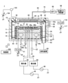
図1Bは、一実施形態に係るプラズマ処理装置1の他の例を示す図である。図1Bでは、遮蔽部材42の内部に電極42aが設けられている。電極42aには、可変直流電源117が電気的に接続され、可変直流電源117から直流電圧が印加される。可変直流電源117には、LF及びHFの電流をカットし、可変直流電源117を保護するローパスフィルタ118が接続されている。
FIG. 1B is a diagram showing another example of the
また、可変直流電源115は、一つに限られず、二つ以上がデポシールドや天井壁等の少なくともいずれかのパーツに接続されてもよい。図1Aには、一例として、エッジリング24の上方の外側に専用のパーツ101が配置されている。パーツ101は内部に電極を有し、可変直流電源104が電気的に接続され、可変直流電源104からその電極に直流電圧が印加される。可変直流電源104には、LF及びHFの電流をカットし、また、可変直流電源104を保護するローパスフィルタ103が接続されている。パーツ101は、リング状であってもよいし、円弧状であってもよいし、その他の形状であってもよい。パーツ101は、例えば、シリコン(Si)やシリコンカーバイト(SiC)から構成される。
Further, the number of variable
[制御部の構成]
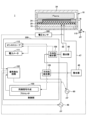
制御部200の具体的構成について、図2を参照して説明する。制御部200は、プロセッサ100、信号発生回路102、方向性結合器105,108、電力メータ111、オシロスコープ112を有する。ただし、電力メータ111、オシロスコープ112、方向性結合器108は設けなくてもよい。
[Configuration of control unit]
A specific configuration of the
第1の高周波電源48の給電ラインには、第1の高周波電源48と整合器46の間に方向性結合器105が接続されている。第2の高周波電源90の給電ラインには、第2の高周波電源90と整合器88の間に方向性結合器108が接続されている。
A
方向性結合器105は、LFの進行波パワーの一部をオシロスコープ112に与える。方向性結合器108は、HFの進行波パワーの一部をオシロスコープ112に与える。一実施形態において、オシロスコープ112に表示されるLFの周波数は、例えば400kHzであり、HFの周波数は、例えば100MHzである。これにより、オシロスコープ112では、LFの進行波の波形とHFの進行波の波形を観察できる。
方向性結合器108は、HFの進行波の一部を電力メータ111に与える。電力メータ111は、HFの進行波の電力量を計量する。
方向性結合器105は、LFの進行波の一部をプロセッサ100に与える。プロセッサ100は、LFの進行波に同期させるDC用(可変直流電源用)の同期信号を作成する。例えば、プロセッサ100は、LFの進行波の正のタイミングに同期させてDC用の同期信号を作成してもよい。なお、方向性結合器105の替わりに、前記センサを用いて検出したLF電力をプロセッサ100に与えてもよい。
プロセッサ100は、作成した同期信号を信号発生回路102に与える。信号発生回路102は、与えられた同期信号からLFの進行波に同期する制御信号を発生し、可変直流電源115及び第1の高周波電源48に与える。
制御信号の生成方法には、以下の2通りがある。第1の高周波電源48が一般的な電源の場合、方向性結合器105が第1の高周波電源48から出力されるLF電力の位相に同期する波形を取り出し、プロセッサ100に入力する。ただし、これに限られず、プロセッサ100が、第1の高周波電源48から直接、LF電力の位相に同期する波形を入力してもよい。LF電力の位相に同期する波形、LF電圧又はLF電流の位相に同期する波形、及びDCパルスの電力、電圧又は電流の位相に同期する波形を以下、バイアス波形ともいう。DCパルスは、LFの電圧のピークに対応するパルス状の電圧をいう。所望の波形のバイアスパワーは、バイアス波形のLFパワーに相当する。
There are two ways to generate the control signal: If the first high-
プロセッサ100は、入力した波形の信号に同期させて又は該信号から任意の遅延と任意の幅を有するオン信号を作成し、信号発生回路102に送信する。プロセッサ100は、第1の高周波電源48からLF電力の位相に同期する波形を入力せずに、第1の高周波電源48を制御するためのLFの信号を自ら生成し、そのLFの信号に同期させて又は該信号から任意の遅延と任意の幅を有するオン信号とを作成してもよい。オン信号は、同期信号の一例である。
The
信号発生回路102は、オン信号の間、直流電圧を発生させるために可変直流電源115に指令信号を送る。指令信号には、可変直流電源115の入力形態に応じて、オン信号の間、直流電圧を発生させる制御信号又はオン信号そのものが使用される。同様に、信号発生回路102は、オン信号の間、HF電力を発生させるために指令信号を第2の高周波電源90に送信してもよい。
第1の高周波電源48がLF電力、電圧又は電流を増幅するアンプの場合、方向性結合器105からの信号は使用せず、信号発生回路102が第1の高周波電源48から出力されるLF電力の位相に同期する波形LFの一部を波形として取り出し、該波形の信号から任意の遅延と任意の幅を有するオン信号を作成してもよい。信号発生回路102は、該波形の信号及びオン信号を可変直流電源115に送信する。
When the first high-
例えば、可変直流電源115の替わりに図示しない交流電源を備え、交流電源をデポシールド等のパーツに電気的に接続し、制御(オン)信号に基づき交流電源から高周波電圧をデポシールド等のパーツに印加してもよい。可変直流電源115及び交流電源は、パーツに所望の波形の電圧を供給する電源の一例である。交流電源は、第2の高周波電源90であってもよいし、別のRF電源であってもよい。
For example, an AC power source (not shown) is provided in place of the variable
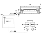
また、図3Aに示すように、第1の高周波電源48から出力されるLF電力の位相に同期する波形を制御部200に設けられた位相シフト回路210に入力し、位相シフト回路210にてLFの位相を所定量シフトさせた高周波電圧をデポシールド等のパーツに印加してもよい。
Further, as shown in FIG. 3A, a waveform synchronized with the phase of the LF power output from the first high-
位相シフト回路210にてLFの位相を所定量シフトする替わりに、第1の高周波電源48から出力されるLFの波形から任意の遅延と任意の幅を有する高周波電圧を生成し、生成した高周波電圧をデポシールド等のパーツに印加してもよい。
Instead of shifting the phase of the LF by a predetermined amount in the
ただし、以上の制御信号の生成方法は一例であり、これに限られない。与えられた周期的に変動するパラメータの各周期内の部分期間に直流電圧と高周波電圧との少なくともいずれかを印加するように制御する制御信号を生成できれば、図2に示す制御部200の回路に限られず、他のハードウェア又はソフトウェアを使用できる。直流電圧の場合、例えば、オンとオフとが交互に繰り返させるように制御する制御信号を生成してもよい。
However, the above control signal generation method is only an example, and is not limited thereto. If it is possible to generate a control signal that controls the application of at least one of a DC voltage and a high-frequency voltage during a partial period within each period of a given periodically varying parameter, the circuit of the
第1の高周波電源48のアンプは、400kHzのLFの変調信号の振幅(AM:amplitude modulation)を増幅し、下部電極に供給する。第2の高周波電源90のアンプは、100MHzのHFの変調信号の振幅を増幅し、下部電極に供給する。
The amplifier of the first high
信号発生回路102は、与えられた同期信号からバイアスパワーの伝達経路で測定される、周期的に変動するパラメータの各周期内の部分期間に直流電圧を印加し、直流電圧の絶対値がHighとLowとが交互に繰り返されるように制御する制御信号を発生し、可変直流電源115に与えてもよい。プロセッサ100は、LFが印加されていない場合、HFの進行波の正のピークとなるタイミングに同期させてDC用の同期信号を作成してもよい。
The
信号発生回路102は、与えられた同期信号からバイアスパワーの伝達経路で測定される、周期的に変動するパラメータの各周期内の部分期間に高周波電圧を印加し、高周波電圧がHighとLowとが交互に繰り返されるように制御する制御信号を発生し、可変直流電源115に与える。部分期間は、電極の電位が正のピークとなるタイミングを含んでもよいし、電極の電位が負のピークとなるタイミングを含んでもよいし、その両方のタイミングを含んでもよい。例えば、図3B及び図3Cは、バイアスパワーの伝送経路(給電系)で測定された電圧、電流又は電磁界のいずれかを「基準電気状態」とする場合の一例である。例えば図3Bでは、プロセッサ100が伝送経路に取り付けられたVIプローブ等のセンサからHFの電圧又は電流、LFの電圧又は電流、HFの位相信号又はLFの位相信号のいずれかを入力する。プロセッサ100は、入力したHFの電圧又は電流、LFの電圧又は電流、HFの位相信号又はLFの位相信号のいずれかを示す基準電気状態の一周期内の位相と同期して直流電圧を第1の状態と第2の状態に交互に印加する。
The
プロセッサ100は、センサからの信号に基づかずに第1の高周波電源48から出力されるバイアスパワーの高周波若しくはパルス波の周期に同期する信号を利用して生成してもよい。この場合、該信号の状態を基準電気状態とすることができる。また、バイアスパワーの給電系で基準電気状態を測定する工程を省くことができる。例えば図3Cでは、プロセッサ100が、第1の高周波電源48からLFの位相信号(小電力波形)又はバイアスパワーの情報に関する信号を入力し、この入力信号に基づきバイアスパワーの高周波若しくはパルス波の周期に同期する信号を生成する。プロセッサ100は、生成した信号を可変直流電源115に出力する。可変直流電源115は、この信号に基づき直流電圧を第1の状態と第2の状態に交互に印加する。
The
なお、図3Dに示すように、プロセッサ100は、第1の高周波電源48からの信号を用いずに、第1の高周波電源48を制御するための信号を生成し、その生成した信号に同期する信号を生成することで、第1の高周波電源48から出力されたバイアスパワーの高周波若しくはパルス波の周期に同期する信号を生成してもよい。この場合、プロセッサ100は、第1の高周波電源48を制御するLFの信号を生成するとともに、この生成した信号に同期する直流電圧の信号を生成する。プロセッサ100は、生成したLFの信号を第1の高周波電源48に送信し、生成した直流電圧の信号を可変直流電源115に送信する。第1の高周波電源48は、LFの信号に基づきバイアスパワーを出力する。可変直流電源115は、直流電圧の信号に基づき直流電圧を第1の状態と第2の状態に交互に印加する。生成したLFの信号及び直流電圧の信号には、パワー情報が含まれる。
Note that, as shown in FIG. 3D, the
[電極電位とイオンの衝突エネルギーとの関係]
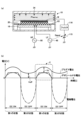
次に、電極電位とイオンの衝突エネルギーとの関係について図4を参照して説明する。第1の高周波電源48から正弦波でLF電力を印加した場合、LFの電圧が負のときにはLFの電圧が正のときよりも自己バイアスVdcによって電圧が負に深くなる。これにより、図4に示すように、LF電力が印加される電極電位が正のときには、その電極電位が側壁の電位(グランド)よりも高くなる。プラズマ電位は、処理容器10内のもっとも高い電位よりも若干高い電位をとるから、電極電位が正のときにはプラズマ電位は電極電位よりも若干高くなる。そのときのプラズマ電位と側壁との電位差Vbを図4の枠B内に示す。
[Relationship between electrode potential and ion collision energy]
Next, the relationship between electrode potential and ion collision energy will be explained with reference to FIG. 4. When LF power is applied in the form of a sine wave from the first high
一方、LF電力が印加される電極電位が負のときには、自己バイアスVdcにより電極電位が側壁の電位(グランド)よりも低くなる。このとき、プラズマ電位は側壁の電位よりも若干高くなる。そのときのプラズマ電位と側壁との電位差Vaを図4の枠A内に示す。これにより、電極電位が正のときのプラズマ電位と側壁との電位差Vbは電極電位が負のときのプラズマ電位と側壁との電位差Vaよりも大きくなる。このため、電極電位が正のとき、側壁へ向かうイオンの加速電圧は大きくなり、側壁への1個当たりのイオンの衝突エネルギーが大きくなる。この結果、側壁へのスパッタが発生しやすくなる。よって、電極電位に応じてプラズマ電位と側壁及び天井壁との電位差を制御することで、加速電圧を制御すれば1個のイオンの衝突エネルギーを制御でき、側壁及び天井壁へのスパッタ力を制御できる。例えば、プラズマ電位と側壁及び天井壁との電位差を大きく制御すれば、図4の(a)の矢印に示すように、側壁及び天井壁へのスパッタ力を強めることができる。一方、その電位差を小さく制御すれば、図4の(b)の矢印に示すように、側壁及び天井壁へのスパッタ力を弱めることができる。 On the other hand, when the electrode potential to which LF power is applied is negative, the electrode potential becomes lower than the side wall potential (ground) due to the self-bias Vdc. At this time, the plasma potential becomes slightly higher than the side wall potential. The potential difference Va between the plasma potential and the side wall at that time is shown in frame A of FIG. Thereby, the potential difference Vb between the plasma potential and the side wall when the electrode potential is positive becomes larger than the potential difference Va between the plasma potential and the side wall when the electrode potential is negative. Therefore, when the electrode potential is positive, the accelerating voltage for ions toward the sidewall increases, and the collision energy of each ion against the sidewall increases. As a result, sputtering tends to occur on the sidewalls. Therefore, by controlling the potential difference between the plasma potential and the side wall and ceiling wall according to the electrode potential, the collision energy of a single ion can be controlled by controlling the acceleration voltage, and the sputtering force on the side wall and ceiling wall can be controlled. can. For example, by controlling the potential difference between the plasma potential and the side walls and the ceiling wall to a large extent, the sputtering force applied to the side wall and the ceiling wall can be strengthened, as shown by the arrow in FIG. 4(a). On the other hand, if the potential difference is controlled to be small, the sputtering force applied to the side walls and ceiling wall can be weakened, as shown by the arrow in FIG. 4(b).
そこで、一実施形態にかかるプラズマ処理装置1の制御方法では、バイアスパワーを下部電極へ供給し、可変直流電源115からの直流電圧をデポシールド11などのパーツに供給する。また、本制御方法は、直流電圧が、第1の電圧値を有する第1の状態と、第1の電圧値よりも高い第2の電圧値を有する第2の状態とを周期的に繰り返す工程と、電極の電位の各周期内の部分期間に第1の電圧値を印加し、第1の状態と第2の状態とが連続するように第2の電圧値を印加する工程とを有する。直流電圧が、第1の状態と、第2の状態と、2つ以上の電圧値を有する2以上の状態とを周期的に繰り返し、電極の電位の各周期内の部分期間に第1の電圧値を印加し、第1の状態と第2の状態と2以上の状態とが連続するように第2の電圧値、2つ以上の電圧値を順に印加する工程を有してもよい。
Therefore, in the control method for the
制御部200は、電極電位の周期と同期する同期信号を作成し、該同期信号から直流電圧を出力する直流電源用の制御信号を生成し、可変直流電源115と位相シフト回路210との少なくともいずれかに送信する。電極の電位の周期とは、バイアス波形の周期に同期する。これにより、制御部200は、可変直流電源115と位相シフト回路210との少なくともいずれかからデポシールド11などのパーツに直流電圧を供給する。例えば、直流電圧が、第1の電圧値を有する第1の状態と、前記第1の電圧値よりも高い第2の電圧値を有する第2の状態とを周期的に繰り返し、前記電極の電位の各周期内の部分期間に前記第1の電圧値を印加し、前記第1の状態と前記第2の状態とが連続するように前記第2の電圧値を印加する第1制御手順を含むプログラムを有する記憶媒体を用意する。そして、制御部200は、記憶媒体のプログラムを実行する。以下では、可変直流電源115に直流電圧を印加する場合を例に挙げて説明する。
The
[DCの電圧の供給タイミング]
本実施形態におけるDCの電圧の供給タイミングの効果について、図5を参照しながら説明する。図5は、一実施形態に係る直流電圧の印加方法(スパッタ制御)とその効果の一例を示す図である。以下では、LFの電圧及びDCの電圧を制御したときの、LFの電圧を印加した電極電位とプラズマ電位、デポシールド11の電位について説明する。
[DC voltage supply timing]
The effect of the DC voltage supply timing in this embodiment will be explained with reference to FIG. 5. FIG. 5 is a diagram illustrating an example of a DC voltage application method (sputter control) and its effects according to an embodiment. Below, when the LF voltage and the DC voltage are controlled, the electrode potential to which the LF voltage is applied, the plasma potential, and the potential of the
(スパッタ抑制)
図5(b)の横軸には時間が示され、縦軸にはLFの電圧を供給したときの電極電位、プラズマ電位、デポシールド11の電位が示されている。電極電位は、LFの電圧にほぼ等しい。図5(b)のCの枠内に示すように、LFの電圧が正のときには可変直流電源115から正の直流電圧がデポシールド11に印加される。これにより、プラズマ電位とデポシールド11の電位差を小さくでき、図5(a)に矢印で示すように側壁へのスパッタ力を抑制できる。
(spatter suppression)
The horizontal axis of FIG. 5(b) shows time, and the vertical axis shows the electrode potential, plasma potential, and potential of the
図5(b)に示すように、LFの電圧が負のときには可変直流電源115からの直流電圧の印加は停止され、デポシールド11に印加される直流電圧は0になる。直流電圧は、電極電位が正のタイミングに一致させた矩形波だけでなく、立ち上がりのスローアップ又は立ち下がりのスローダウンの少なくともいずれかを含む略矩形波を印加してもよい。
As shown in FIG. 5(b), when the voltage of LF is negative, the application of the DC voltage from the variable
制御部200は、電極電位の周期と同期する同期信号からLFの電圧が正のときに正の直流電圧を印加し、LFの電圧が負のときに直流電圧の印加を停止する直流電源用の制御信号を生成し、可変直流電源115に送信する。LFの電圧が正のときに正の直流電圧を印加する状態は第1の状態の一例であり、LFの電圧が負のときに直流電圧の印加を停止する状態は第2の状態の一例である。制御信号を受信すると、可変直流電源115は、直流電圧の第1の状態と第2の状態とを電極電位の周期と同期して交互に印加する。
The
LF電力が印加される電極電位が負のときには可変直流電源115からの直流電圧の印加は停止され、プラズマ電位とデポシールド11との電位差Voffが、側壁へ向かうイオンを加速する加速電圧となる。よって、側壁への1個当たりのイオンの衝突エネルギーは電位差Voffによって定まる。
When the electrode potential to which the LF power is applied is negative, the application of the DC voltage from the variable
一方、図5(b)の枠C内に示す電極電位が正のときには、可変直流電源115からの直流電圧はオンされ、正の直流電圧がデポシールド11に印加される。そうすると、プラズマ電位とデポシールド11との電位差Vcが加速電圧となり、側壁への1個当たりのイオンの衝突エネルギーは電位差Vcによって定まる。プラズマ電位とデポシールド11との電位差Vcは、可変直流電源115からの正の直流電圧がデポシールド11に印加されない場合と比較して小さくなる。このため、側壁への1個当たりのイオンの衝突エネルギーは、正の直流電圧がデポシールド11に印加した場合、印加されない場合と比較して低くなる。このように、電極の電位が負のときにはプラズマ電位とデポシールド11との電位差Voffは小さい。これに対して、可変直流電源115からの正の直流電圧をオンしないと、電極の電位が正のときには電極電位が壁の電位よりも大きくなるためにプラズマ電位とデポシールド11との電位差が大きい。このため、可変直流電源115からの正の直流電圧をオンし、プラズマ電位とデポシールド11との電位差を小さくするように制御することで、側壁へのスパッタ力を抑制することができる。これにより、処理容器10内の下部電極と比較して側壁の面積を大きくすることで、カソード/アノード比を制御し、単位面積当たりの1個のイオンの衝突エネルギーを小さく見せる制御と同様な制御が可能になる。これにより、単位面積当たりの1個のイオンの衝突エネルギーを小さくすることで、側壁へのスパッタによるプロセスへの影響を小さくすることができる。なお、第1の状態と第2の状態は、可変直流電源115からの正の直流電圧をオン・オフすることで設定する制御に限られない。第1の状態と第2の状態は、可変直流電源115からの正の直流電圧をHigh・Lowにすることで設定するように制御してもよい。
On the other hand, when the electrode potential shown in frame C in FIG. Then, the potential difference Vc between the plasma potential and the
側壁へのイオンの衝突エネルギーを減らしたい場合、電極電位が正のときにデポシールド11へ正の直流電圧をオンに制御することで、電極電位が正のときにイオンが側壁を叩く効果を低減することができる。このようにして側壁へのイオン衝突エネルギーを抑制することでチャンバの側面の寿命を延ばすことができる。また、側壁へのイオン衝突エネルギーを抑制することでパーティクルを低減できる。また、側壁へのイオン衝突エネルギーを抑制することで、クリーニングサイクルを伸ばすことができる。
If you want to reduce the energy of ions colliding with the side wall, turn on the positive DC voltage to the
また、電極電位が負のときに正の直流電圧をオフに制御することで、電極電位が負のときにイオンがウエハWを叩くエネルギーを維持することができる。 Further, by controlling the positive DC voltage to be turned off when the electrode potential is negative, it is possible to maintain the energy of ions hitting the wafer W when the electrode potential is negative.
(クリーニング/特定のプロセス)
以上に説明した第1の状態の期間は、電極電位が正のピークとなるタイミングを含み、正又は負の直流電圧を前記パーツに印加してもよい。第1の状態の期間は、電極電位が負のピークとなるタイミングを含み、正又は負の直流電圧を前記パーツに印加してもよい。
(cleaning/specific process)
The period of the first state described above includes the timing at which the electrode potential reaches a positive peak, and a positive or negative DC voltage may be applied to the part. The period of the first state includes a timing when the electrode potential reaches a negative peak, and a positive or negative DC voltage may be applied to the part.
図6は、一実施形態に係る電極電位の正負とイオンの衝突エネルギーの一例を示す図である。図6(c)の枠H内に示すように、例えば、電極電位が正のときに正の直流電圧をデポシールド11及び天井壁(例えば、遮蔽部材42)へ印加した場合、プラズマ電位とデポシールド11の電位との電位差がH1からH2へ小さくなり、側壁への1個当たりのイオンの衝突エネルギーが下がる。その結果、側壁及び天井壁へのスパッタ力を弱めることができる。一方、電極電位が正のときに負の直流電圧をデポシールド11及び天井壁へ印加した場合、プラズマ電位とデポシールド11の電位との電位差が大きくなり、側壁への1個当たりのイオンの衝突エネルギーが上がる。その結果、側壁及び天井壁へのスパッタ力を強めることができる。このようにして、図6(a)に示すように側壁及び天井壁への1個当たりのイオンの衝突エネルギーを制御できる。
FIG. 6 is a diagram illustrating an example of positive/negative electrode potential and ion collision energy according to an embodiment. As shown in frame H in FIG. 6(c), for example, if a positive DC voltage is applied to the
また、図6の枠G内に示すように、電極電位が負のときに直流電圧をデポシールド11及び天井壁へ印加することによって、図6(b)に示すように、ウエハWへの1個当たりのイオンの衝突エネルギーを制御できる。例えば、図7(b)に示すように、電極電位が負のときに正の直流電圧をデポシールド11へ印加すると、プラズマ電位と電極電位との電位差が大きくなり、図7(a)の矢印に示すように、ウエハWへの1個当たりのイオンの衝突エネルギーが上がる。これにより、プロセスの効率化を図ることができる。たとえば、MRAMの製造では、数十層のメタルをエッチングする。このようにウエハに高いイオンエネルギーを持ったイオンを叩き着けて深く穴をエッチングしたいプロセスがある。かかるプロセスでは、電極電位が正のときには直流電圧の印加を停止し、電極電位が負のときに正の直流電圧をデポシールド11に印加することで高いイオンエネルギーを持ったイオンをウエハWに叩きつけることができる。これにより、当該プロセスでのウエハへのイオンの衝突エネルギーを上げてプロセスの処理効率を高め、生産性を向上させることができる。
In addition, as shown in the frame G of FIG. 6, by applying a DC voltage to the
クリーニング処理時には、電極電位が正のときに負の直流電圧をデポシールド11へ印加し、側壁への1個当たりのイオンの衝突エネルギーを上げ、電極電位が負のときに直流電圧のデポシールド11への印加を停止する。これにより、側壁へのイオン衝突エネルギーを増加又は変更させて最適なイオンエネルギーに制御することで、クリーニングサイクルを伸ばすことができ、かつ、クリーニング時間を短縮することができる。なお、クリーニング処理時には、電極電位が正のときに負の直流電圧をデポシールド11に印加し、電極電位が負のときには直流電圧の印加を停止する制御に限られず、電極電位が負のときにも電極電位が正のときと同じ負の直流電圧を連続して印加してもよい。電極の電位が負のときに負のDCをデポシールド11へ印加すると、プラズマ電位と電極電位との電位差が小さくなり、ウエハへの1個当たりのイオンの衝突エネルギーが下がる。これにより、WLDCのクリーニングにおいては、ウエハを載置する載置台の載置面へのダメージを軽減できる。
During the cleaning process, when the electrode potential is positive, a negative DC voltage is applied to the
また、たとえば側壁の副生成物や天井壁のスパッタ物をウエハに堆積させたいプロセスの場合、電極電位が正のときに負の直流電圧をデポシールド11へ印加することで、イオンを壁面に叩き易くすることで、副生成物等をウエハに堆積させることができる。他方、たとえば側壁の副生成物等をウエハに堆積させたくないプロセスや、側壁のスパッタを極力行いたくないプロセスの場合、電極電位が正のときに正の直流電圧をデポシールド11へ印加し、イオンをウエハに叩き難くすることで、副生成物等をウエハに堆積させないようにすることができる。
In addition, for example, in the case of a process in which by-products on the side walls or sputtered materials on the ceiling wall are to be deposited on the wafer, by applying a negative DC voltage to the
このようにデポシールド11への直流電圧の正・負及び大きさにより側壁へのイオンの衝突エネルギーを制御することで、高いバイアスパワーを印加する制御が可能になる。さらに、上記直流電圧の正・負及び大きさの制御とともに、供給するバイアスパワーをさらに上げて印加してもよい。
In this way, by controlling the impact energy of ions on the side wall by the positive/negative and magnitude of the DC voltage applied to the
複数の可変直流電源を用いて直流電圧を複数のパーツに印加してもよい。例えば、図8(a)に示すように可変直流電源115が処理容器10のデポシールド11に電気的に接続され、可変直流電源117が処理容器10の天井壁のパーツに電気的に接続されてもよい。可変直流電源115には、LF及びHFの電流をカットし、可変直流電源115を保護するローパスフィルタ116が接続されている。可変直流電源117には、LF及びHFの電流をカットし、可変直流電源117を保護するローパスフィルタ118が接続されている。
A plurality of variable DC power supplies may be used to apply a DC voltage to a plurality of parts. For example, as shown in FIG. 8(a), a variable
例えば、下部電極にLF電力及びHF電力が印加される場合、上部電極に副生成物が付着しやすい。そこで、副生成物が付着しやすい天井壁に接続された可変直流電源117には、図8(b)のEに示すように、電極電位が正のときに負の直流電圧をデポシールド11に印加する。これにより、プラズマ電位と天井壁の電位との電位差を大きくし、天井壁へのイオンの衝突エネルギーを上げることで天井壁へのスパッタ力を高め、天井壁に付着した副生成物を除去し易くする。また、副生成物が天井壁よりも付着しにくいデポシールド11に接続された可変直流電源115には、図8(b)のDに示すように、電極電位が正のときに正の直流電圧をデポシールド11に印加する。これにより、プラズマ電位とデポシールド11の電位との電位差を小さくし、側壁へのイオンの衝突エネルギーを下げ、側壁へのスパッタ力を弱めることができる。この結果、複数のパーツによって副生成物の付着量が異なる場合であっても、複数の可変直流電源115,117を用いてパーツ毎に適切に副生成物を除去し、クリーニング時間を同じにすることができる。
For example, when LF power and HF power are applied to the lower electrode, byproducts tend to adhere to the upper electrode. Therefore, when the electrode potential is positive, the variable
また、上部電極と側壁とでは温度が異なり、上部電極は側壁よりも温度が高くなる。つまり、上部電極の近傍にはプラズマが生成されるため、温度が高く、かつイオンの数が多い。これに対して側壁は、上部電極よりも温度が低く、かつイオンの数も少ない。イオンの衝突エネルギーは、温度と加速電圧で決まるから、これを考慮し複数系統の可変直流電源からの複数のパーツへの直流電圧を制御することが好ましい。 Further, the temperature of the upper electrode and the side wall is different, and the temperature of the upper electrode is higher than that of the side wall. That is, since plasma is generated near the upper electrode, the temperature is high and the number of ions is large. On the other hand, the side wall has a lower temperature and fewer ions than the upper electrode. Since the collision energy of ions is determined by temperature and accelerating voltage, it is preferable to take this into account and control the DC voltages from multiple systems of variable DC power supplies to multiple parts.
[制御方法]
以上に説明したように、一実施形態に係る平行平板型のプラズマ処理装置1の制御方法は、バイアスパワーを、ウエハWを載置する載置台16に供給する工程と、直流電圧を処理容器内のプラズマに暴露されるパーツに供給する直流電源に供給する工程とを含む。
[Control method]
As described above, the control method for the parallel plate
本制御方法では、直流電圧は、第1の電圧値を有する第1の状態と、前記第1の電圧値よりも高い第2の電圧値を有する第2の状態とを周期的に繰り返し、電極の電位の各周期内の部分期間に前記第1の電圧値を印加し、前記第1の状態と前記第2の状態とが連続するように前記第2の電圧値を印加する。電極の電位は、前記バイアスパワーの伝達経路で測定される、周期的に変動するパラメータにより定められ、前記周期的に変動するパラメータは、電圧、電流、電磁界、発生したプラズマの発光の変化又は被処理体上のプラズマのシース厚の変化であってもよい。 In this control method, the DC voltage periodically repeats a first state having a first voltage value and a second state having a second voltage value higher than the first voltage value, and The first voltage value is applied during a partial period within each cycle of the potential, and the second voltage value is applied so that the first state and the second state are continuous. The potential of the electrode is determined by a periodically varying parameter measured in the transmission path of the bias power, and the periodically varying parameter may be a change in voltage, current, electromagnetic field, light emission of generated plasma, or It may also be a change in the sheath thickness of the plasma on the object to be processed.
例えば、図8の例では、デポシールド11の電位が第1の状態になるように、電極電位を一例とする周期的に変動するパラメータが正の値を含む部分期間にDCの電圧を印加し、第2の状態を第1の状態と連続して印加する。図5、図7、図8、デポシールド11、図10Aでは、DCの電圧の第1の状態が正(又は負)の電圧値であり、第2の状態が0である。図10Bでは、DCの電圧の第1の状態が正の電圧値であり、第2の状態が負の電圧値である。
For example, in the example of FIG. 8, a DC voltage is applied during a partial period in which a periodically varying parameter, for example the electrode potential, has a positive value so that the potential of the
図5、図7~図10Aに示すように、パーツへ印加する直流電圧がオン(DC ON、つまり、DCが正又は負に印加)されている状態は、第1の電圧値を有する第1の状態の一例である。パーツへ印加する直流電圧がオフ(DC OFF、つまり、DCが0)又は第1の状態と異なる電圧値とされている状態は、第1の電圧値よりも高い第2の電圧値を有する第2の状態の一例である。 As shown in FIGS. 5 and 7 to 10A, when the DC voltage applied to the parts is on (DC ON, that is, DC is applied positively or negatively), a first voltage having a first voltage value is applied. This is an example of the state. A state in which the DC voltage applied to the part is off (DC OFF, that is, DC is 0) or at a voltage value different from the first state is a state in which the DC voltage applied to the part is set to a voltage value different from the first state. This is an example of state 2.
なお、第1の状態及び第2の状態は、パーツへ印加する直流電圧がオン及びオフに制御される状態に限られず、電圧値の絶対値がLow及びHighに制御される状態を含む。 Note that the first state and the second state are not limited to states in which the DC voltage applied to the parts is controlled to be on and off, but include states in which the absolute value of the voltage value is controlled to be low and high.
第1の状態の期間は、第1の電極又は第2の電極の電位が正のピークとなるタイミングを含み、正又は負の直流電圧を前記パーツに印加してもよい。また、第1の状態の期間は、第1の電極又は第2の電極の電位が負のピークとなるタイミングを含み、正又は負の直流電圧を前記パーツに印加してもよい。 The period of the first state includes a timing when the potential of the first electrode or the second electrode reaches a positive peak, and a positive or negative DC voltage may be applied to the part. Further, the period of the first state includes a timing when the potential of the first electrode or the second electrode reaches a negative peak, and a positive or negative DC voltage may be applied to the part.
また、直流電圧は、電極電位が正のタイミングから任意の遅延と任意の幅を有するタイミングに前記パーツに印加してもよい。例えば、電極電位が正のタイミングから所定時間だけ後にずらしたタイミング又は所定時間だけ前にずらしたタイミングの少なくともいずれかに前記パーツに印加してもよい。電極電位の特に正側の波形は、LFの周波数やガス種や圧力に依存して歪む場合がある。このような場合は、電極電位が正のタイミングから所定時間だけずらして、よりシースが薄く電子が入りやすい位相を選定して直流電圧を印加することが好ましい。また、直流電圧は、電極電位が正のタイミングに対して所定時間だけ長く又は短くするように印加時間の幅を調整してもよい。 Further, the DC voltage may be applied to the part at a timing having an arbitrary delay and an arbitrary width from the timing when the electrode potential is positive. For example, the voltage may be applied to the part at least at a timing shifted a predetermined time later or a predetermined time earlier than the timing when the electrode potential is positive. The waveform of the electrode potential, particularly on the positive side, may be distorted depending on the LF frequency, gas type, and pressure. In such a case, it is preferable to apply the DC voltage by shifting the timing at which the electrode potential is positive by a predetermined time and selecting a phase in which the sheath is thinner and electrons can more easily enter. Further, the width of the application time of the DC voltage may be adjusted so as to be longer or shorter by a predetermined time with respect to the timing when the electrode potential is positive.
LFの電圧の周期と同期して、直流電圧とHFの電圧との両方を、オン・オフ又はHigh・Lowに制御してもよい。このとき、電極電位が正又は負のいずれか一方のタイミングにHFの電圧を供給し、電極電位が正又は負のいずれか他方のタイミングにHFの電圧の供給を停止してもよい。直流電圧の印加タイミングと同じタイミングでHFの電圧を制御してもよい。 Both the DC voltage and the HF voltage may be controlled to be on/off or high/low in synchronization with the period of the LF voltage. At this time, the HF voltage may be supplied at one timing when the electrode potential is positive or negative, and the supply of the HF voltage may be stopped at the other timing when the electrode potential is positive or negative. The HF voltage may be controlled at the same timing as the DC voltage application timing.
また、例えばWLDCのクリーニング処理において載置台16のダメージを低減するためにLF電力を印加しない場合がある。そのときには、制御部200は、前記直流電圧の第1の状態と第2の状態とを電極電位と同期させるために、ソースパワーの周期と同期して交互に印加してもよい。特に、上部電極にHFの電圧を印加することでWLDC時のウエハへのダメージを減らすことができる。このとき、載置台16は壁として見なされる。載置台16にRFパワーを印加するRF電源を別途設け、上部電極の電位が高いときに、載置台16にRF電源からRFパワーを印加し、ウエハ電位を高く制御してもよい。これにより、上部電極の電位とウエハ電位との電位差を小さく制御して、載置台16へのダメージを抑制できる。この場合、LFの周波数と同じかそれよりも高い周波数のRFパワーを印加することが好ましい。
Further, in order to reduce damage to the mounting table 16 in cleaning processing of the WLDC, for example, LF power may not be applied. At that time, the
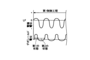
[変形例1-1~1-3]
次に、一実施形態の変形例1-1~1-3に係るプラズマ処理装置1の制御方法について説明する。図9、図10A、図10Bは、一実施形態の変形例1-1~1-3に係る制御方法を示すタイミングチャートである。図9の変形例1-1では、DCパルスの電圧は、第1制御工程において第1の状態と第2の状態とを交互に1回以上繰り返す。第1制御工程では、LFの周波数は、例えば0.1Hz~100Hzであってもよい。
[Modifications 1-1 to 1-3]
Next, a method of controlling the
図9の変形例1-1では、LFの電圧の替わりにDCパルスが載置台16に印加される。DCパルスの電圧の正の値は、LFの電圧の正のピークに一致し、DCパルスの電圧の負の値又は0は、LFの電圧の負のピークに一致し、デポシールド11に印加する直流電圧が第1の状態と第2の状態とになるようにDCパルスの電圧に同期して直流電圧を交互に印加する。具体的には、DCパルスの電圧が正のタイミングにデポシールド11の電位は第1の状態になり、DCパルスの電圧が負のタイミングにデポシールド11の電位が第2の状態になるように直流電圧を制御してもよい。これによれば、DCパルスの電圧が2値化されており、これに応じて直流電圧を2値化して制御するため、直流電圧の印加の制御が容易になる。なお、直流電圧を周期的にオン・オフする替わりに、直流電圧を周期的にHigh・Lowになるように制御してもよい。
In modification 1-1 of FIG. 9, a DC pulse is applied to the mounting table 16 instead of the LF voltage. The positive value of the voltage of the DC pulse corresponds to the positive peak of the voltage of the LF, and the negative value or 0 of the voltage of the DC pulse corresponds to the negative peak of the voltage of the LF applied to the
図10Aの変形例1-2では、直流電圧は、第1の状態において正の値であって段階的に2つ以上の電圧値を有し、第2の状態において0に制御される。また、図10Bの変形例1-3では、直流電圧は、第1の状態において正の値であって滑らかに2つ以上の電圧値を有し、第2の状態において滑らかに負の電圧値を有する。変形例1-2、1-3では、第1の状態又は第2の状態における直流電圧を複数の値に制御することで、より精度良くイオンエネルギーを制御することができる。 In modification 1-2 of FIG. 10A, the DC voltage is a positive value in the first state and has two or more voltage values in stages, and is controlled to 0 in the second state. Further, in Modification 1-3 of FIG. 10B, the DC voltage has a positive value in the first state and smoothly has two or more voltage values, and smoothly changes to a negative voltage value in the second state. has. In Modifications 1-2 and 1-3, by controlling the DC voltage in the first state or the second state to a plurality of values, the ion energy can be controlled with higher accuracy.
上記の実施形態及び各変形例では、電極電位の電圧の周期と同期して直流電圧を印加する制御方法の一例として、バイアスパワーの電圧の周期と同期して直流電圧を印加する制御方法について説明した。しかし、ソースパワーの電圧の周期と同期して直流電圧を印加してもよい。バイアスパワー又はソースパワーの電圧の周期と同期して直流電圧及びソースパワーの電圧の少なくともいずれかを印加してもよい。 In the above embodiment and each modification, a control method of applying a DC voltage in synchronization with the voltage cycle of the bias power is described as an example of a control method of applying a DC voltage in synchronization with the voltage cycle of the electrode potential. did. However, a DC voltage may be applied in synchronization with the period of the source power voltage. At least one of the DC voltage and the source power voltage may be applied in synchronization with the cycle of the bias power or the source power voltage.
以上では、可変直流電源115又は可変直流電源117から処理容器10のデポシールド11に印加する直流電圧についての制御方法を説明したが、これに限られない。例えば、高周波電源(第1の高周波電源48)から処理容器10のデポシールド11に印加する高周波電圧についても直流電圧についての制御方法と同様に制御することができる。
Although the method for controlling the DC voltage applied from the variable
つまり、本実施形態に係るプラズマ処理装置は、処理容器と、処理容器内で被処理体を載置する電極と、処理容器内にプラズマを供給するプラズマ生成源と、電極にバイアスパワーを供給するバイアス電源と、処理容器内のプラズマに暴露されるパーツと、バイアスパワーの電圧の周波数と同一の周波数を有する高周波電圧をパーツに供給する高周波電源と、電極の電位の位相に対して所定の位相差を生じるように高周波電圧を印加する第1制御手順を含むプログラムを有する記憶媒体と、前記記憶媒体のプログラムを実行する制御部とを有してもよい。所定の位相差は、90°~270°であってもよい。 In other words, the plasma processing apparatus according to the present embodiment includes a processing container, an electrode for placing an object to be processed in the processing container, a plasma generation source for supplying plasma into the processing container, and a bias power for supplying bias power to the electrode. A bias power source, a high frequency power source that supplies the parts with a high frequency voltage having the same frequency as the frequency of the bias power voltage, and a predetermined position relative to the phase of the potential of the electrode. The device may include a storage medium having a program including a first control procedure for applying a high frequency voltage so as to generate a phase difference, and a control unit that executes the program on the storage medium. The predetermined phase difference may be between 90° and 270°.
また、バイアス電源から出力する高周波電圧用の制御信号を生成し、生成した前記制御信号を位相シフト回路に送信し、相シフト回路から前記エッジリングに高周波電圧を供給してもよい。 Alternatively, a control signal for a high frequency voltage output from a bias power supply may be generated, the generated control signal may be transmitted to a phase shift circuit, and the high frequency voltage may be supplied from the phase shift circuit to the edge ring.
また、例えば、直流電圧に三角波で出力される電圧を合成するなど、直流電圧に他の電圧を合成した電圧をかけてもよい。 Further, for example, a voltage obtained by combining the DC voltage with another voltage may be applied, such as combining the DC voltage with a voltage output in the form of a triangular wave.
前記プログラムは、CD-ROM、DVD等の可搬性のコンピュータにより読み取り可能な記憶媒体に収容された状態で所定位置にセットされ、制御部により読み出されるようにしてもよい。 The program may be stored in a portable computer-readable storage medium such as a CD-ROM or DVD, set at a predetermined position, and read out by the control unit.
[変形例1-4~1-6]
次に、一実施形態の変形例1-4~1-6に係るプラズマ処理装置1の制御方法について、図11~図13を参照して説明する。図11は、一実施形態の変形例1-4に係る制御方法を示すタイミングチャートである。図12は、一実施形態の変形例1-5に係る制御方法を示すタイミングチャートである。図13は、一実施形態の変形例1-6に係る制御方法を示すタイミングチャートである。
[Modifications 1-4 to 1-6]
Next, a method of controlling the
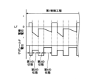
図11に示す変形例1-4では、直流電圧は、LF電圧又はバイアスパワーの一周期を4ゾーンに分け、各ゾーンに応じて所定の値の直流電圧に制御され、デポシールド11に印加される。つまり、第1制御工程において第1ゾーンの第1の状態と、第2ゾーンの第2の状態と、第3ゾーンの第3の状態と、第4ゾーンの第4の状態とをこの順に1回以上繰り返す。これにより、デポシールド11の電位は、4つの状態(固定値)に制御される。変形例1-4では、隣り合うゾーンに印加される電圧は異なる値であって一定の値である。なお、第1制御工程では、LFの周波数は、例えば0.1Hz~100Hzであってもよい。
In Modification 1-4 shown in FIG. 11, the DC voltage is applied to the
図12に示す変形例1-5では、所望の波形のバイアスパワーを使用する。バイアスパワーは、かかるバイアスパワーの波形は、所望の波形(バイアス波形)の一例である。所望のバイアス波形は、図12に示すように任意の波形であり、その一周期を4ゾーンに分け、各ゾーンに応じて所定の値の直流電圧がデポシールド11に印加される。つまり、第1制御工程において第1ゾーンの第1の状態と、第2ゾーンの第2の状態と、第3ゾーンの第3の状態と、第4ゾーンの第4の状態とをこの順に1回以上LFの周期に合わせて繰り返す。これにより、デポシールド11の電位は、4つの状態(固定値)に制御される。変形例1-5では、隣り合うゾーンに印加される電圧は異なる値であって一定の値である。
In modification 1-5 shown in FIG. 12, bias power of a desired waveform is used. The waveform of the bias power is an example of a desired waveform (bias waveform). The desired bias waveform is an arbitrary waveform as shown in FIG. 12, one period of which is divided into four zones, and a DC voltage of a predetermined value is applied to the
図13に示す変形例1-6も、変形例1-5と同一のバイアス波形の一周期を4ゾーンに分け、各ゾーンに応じて所定の値の直流電圧がデポシールド11に印加される。第1制御工程において第1ゾーンの第1の状態と、第2ゾーンの第2の状態と、第3ゾーンの第3の状態と、第4ゾーンの第4の状態とをこの順に1回以上LFの周期に合わせて繰り返す。これにより、デポシールド11の電位は、4つの状態(可変値を含む)に制御される。図13の例では、第1ゾーンで印加される電圧は、始点から終点まで電位が傾斜して変化する可変値である。第2ゾーン~第4ゾーンで印加される電圧は、固定値である。第1ゾーンに示す波形をテーラード波形ともいう。
In Modification 1-6 shown in FIG. 13, one period of the bias waveform, which is the same as Modification 1-5, is divided into four zones, and a DC voltage of a predetermined value is applied to the
以上に説明したように、バイアスパワーを電極に供給するバイアス電源としてLF電力を供給する第1の高周波電源48の替わりに、所望のバイアス波形のバイアスパワーを電極に供給する電源を有してもよい。この場合、バイアス波形のバイアスパワーの一周期を複数のゾーンに分割して各ゾーンに応じて、直流電圧が、第1の電圧値を有する第1の状態と、第1の電圧値と異なる第2の電圧値を有する第2の状態と、第2の電圧値と異なる第3の電圧値を有する第3の状態と、第3の電圧値と異なる第4の電圧値を有する第4の状態と、を周期的に繰り返し、電極の電位の各周期内の部分期間に第1の電圧値を印加し、第1の状態と第2の状態とが連続するように第2の電圧値を印加し、第2の状態と第3の状態とが連続するように第3の電圧値を印加し、第3の状態と第4の状態とが連続するように第2の電圧値を印加する第1制御手順を含むプログラムを有する記憶媒体を有してもよい。そして、制御部200は、その記憶媒体のプログラムを実行してもよい。これにより、バイアス波形の一周期を複数のゾーンに分け、ゾーン毎に固定又は可変の電圧を印加するように制御することで、イオンの衝突エネルギーを制御することができる。バイアス波形の一周期を分けるゾーン数は2以上であればよい。これにより、バイアス波形の一周期に2以上の状態の電圧をデポシールド11等のパーツに印加することができる。
As explained above, instead of the first high
所望のバイアス波形は、LF(RF)、DCパルスに限らない。所望のバイアス波形は、図12及び図13に示すテーラード波形を含む波形であってもよい。バイアス波形の信号は、発信器(図3Cのプロセッサ100参照)で生成し、生成した信号をアンプで増幅して任意の波形のパワーを供給する電源に出力することで生成できる。前述したバイアスパワーは、所望のバイアス波形のパワーの一例である。可変直流電源115は、パーツに所望のバイアス波形の電圧を供給する電源の一例である。可変直流電源115に替えて配置され得る交流電源からパーツに所望のバイアス波形の電圧を供給してもよい。また、第1の高周波電源48も同様に、電極に所望のバイアス波形のパワーを供給するバイアス電源の一例である。載置台16に第2の高周波電源90とは別のRFパワーを印加するRF電源を別途設けてもよい。この場合、第2の高周波電源90及びRF電源は、所望のバイアス波形のパワーの電圧の周波数と同一又は異なる周波数を有する高周波電圧をデポシールド11等のパーツに供給する電源の一例である。
The desired bias waveform is not limited to LF (RF) and DC pulses. The desired bias waveform may be a waveform including the tailored waveforms shown in FIGS. 12 and 13. A bias waveform signal can be generated by generating the signal with an oscillator (see
デポシールド11へ印加する電圧は、直流電圧をオン・オフするだけでなく、高周波RFのパワーを変更してもよいし、図13のデポシールド11の電位に示すように任意に形成されたバイアス波形を印加してもよい。直流電圧及び高周波RFのパワーを制御し、更に高周波RFの周波数を変えてもよい。デポシールド11等のパーツへ印加する電圧は、プロセスレシピに対応して制御部200により制御してもよい。
The voltage applied to the
[変形例2-1~2-4]
次に、一実施形態の変形例2-1~2-4に係るプラズマ処理装置1の制御方法について説明する。変形例2-1~2-4では、バイアスパワーと直流電圧とのいずれか又は両方を間欠的に停止する制御を行う。図14A~図14Dは、一実施形態の変形例2-1~2-4に係る制御方法を示すタイミングチャートである。
[Modifications 2-1 to 2-4]
Next, a method of controlling the
図14Aの変形例2-1では、第1制御工程に加えて、直流電圧を、LF電圧により一例を示す周期的に変動するパラメータの周期と独立した周期で間欠的に停止する第2制御工程を含む。第1制御工程と第2制御工程とは繰り返し実行される。 In modification 2-1 of FIG. 14A, in addition to the first control step, a second control step is performed in which the DC voltage is intermittently stopped at a period independent of the period of the periodically varying parameter, an example of which is shown by the LF voltage. including. The first control step and the second control step are repeatedly executed.
変形例2-1では、LF電圧は、第1制御工程及び第2制御工程において同じ周期で印加される。一方、DCの電圧は、第1制御工程において第1の状態と第2の状態とを交互に1回以上繰り返し、第2制御工程において第1制御工程の間で間欠的に停止される。 In modification 2-1, the LF voltage is applied at the same period in the first control process and the second control process. On the other hand, the DC voltage alternately repeats the first state and the second state one or more times in the first control step, and is intermittently stopped between the first control steps in the second control step.
第1制御工程及び第2制御工程では、LFの周波数は、例えば0.1Hz~100kHzであってもよい。図14Aの変形例2-1~図14Dの変形例2-4では、処理容器のデポシールド11の電位が第1の状態になるように、電極電位を一例とする周期的に変動するパラメータが正の値を含む部分期間に直流電圧を印加し、第2の状態を第1の状態と連続して印加する。直流電圧の場合、正の値であり、第1の状態の第1の電圧値が第2の状態の第2の電圧値よりも高い。
In the first control step and the second control step, the frequency of the LF may be, for example, 0.1 Hz to 100 kHz. In Modification 2-1 of FIG. 14A to Modification 2-4 of FIG. 14D, a periodically varying parameter, for example an electrode potential, is set so that the potential of the
図14Aの変形例2-1~図14Dの変形例2-4では、DCの電圧の第1の状態が正の電圧値を有し、第2の状態が0である。なお、直流電圧のDuty比(=第4の状態/(第3の状態+第4の状態))は、1%~99%の範囲内であればよい。 In Modification 2-1 of FIG. 14A to Modification 2-4 of FIG. 14D, the first state of the DC voltage has a positive voltage value, and the second state is zero. Note that the duty ratio of the DC voltage (=fourth state/(third state + fourth state)) may be within the range of 1% to 99%.
所定の高周波電圧(以下、「RF電圧」ともいう。)を処理容器のデポシールド11へ供給してもよい。この場合、第2の高周波電源90から、RF電圧を処理容器のデポシールド11に供給してもよいし、載置台16にRF電圧を印加するRF電源を別途設けてもよい。RF電圧は、第1の状態の第1の電圧値が第2の状態の第2の電圧値よりも高い。
A predetermined high frequency voltage (hereinafter also referred to as "RF voltage") may be supplied to the
図14Aの変形例2-1において、第1制御工程におけるLF電圧が正のタイミングで同期したDCの電圧が第1の状態をとり、0の第2の状態と繰り返されるのが、第3の状態の一例である。第2制御工程におけるLF電圧の周期と独立したDCの電圧の状態は、第3の状態と異なる第4の状態の一例である。 In modification 2-1 of FIG. 14A, the DC voltage synchronized with the positive timing of the LF voltage in the first control step takes the first state, and repeats the second state of 0, which is the third state. This is an example of the state. The state of the DC voltage independent of the period of the LF voltage in the second control step is an example of a fourth state different from the third state.
図14Bの変形例2-2にかかる制御方法は、変形例2-1と同じ第1制御工程に加えて、バイアスパワーをDCの電圧の周期とは独立した周期で間欠的に停止する第3制御工程を含む。第3制御工程におけるバイアスパワーの状態は、第4の状態の一例である。 The control method according to Modification 2-2 in FIG. 14B includes, in addition to the first control step same as Modification 2-1, a third control step in which the bias power is intermittently stopped at a period independent of the DC voltage period. Includes control process. The bias power state in the third control step is an example of the fourth state.
変形例2-2では、第1制御工程と第3制御工程とが繰り返し実行される。変形例2-2では、第3制御工程におけるDCの電圧は、第1制御工程と同じ周期で第1の状態と第2の状態とが繰り返される。 In modification 2-2, the first control step and the third control step are repeatedly executed. In modification 2-2, the DC voltage in the third control step repeats the first state and the second state at the same period as the first control step.
なお、第1制御工程においてLFの周波数は、例えば0.1Hz~100Hzであってもよく、LFの電圧のDuty比(=第4の状態/(第3の状態+第4の状態))は、1%~90%の範囲内であればよい。 Note that in the first control step, the frequency of the LF may be, for example, 0.1 Hz to 100 Hz, and the duty ratio of the LF voltage (=fourth state/(third state + fourth state)) is , as long as it is within the range of 1% to 90%.
図14Cの変形例2-3にかかる制御方法は、変形例2-1と同じ第1制御工程に加えて、変形例2-1の第2制御工程のDCの制御と変形例2-2の第3制御工程のLFの制御が行われる。つまり、変形例2-3におけるDCの電圧及びバイアスパワーの両方を間欠的に停止した状態は、第4の状態の一例である。 The control method according to Modification Example 2-3 in FIG. 14C includes, in addition to the first control step same as Modification Example 2-1, DC control in the second control step of Modification Example 2-1 and DC control in the second control step of Modification Example 2-2. LF control in the third control step is performed. That is, the state in which both the DC voltage and bias power are intermittently stopped in Modification 2-3 is an example of the fourth state.
バイアスパワーを間欠的に停止する周期とDCの電圧を間欠的に停止する周期とは同期させてもよい。この場合、DC及びバイアスパワーを間欠的に停止する周期は、図14Cに示すように一致してもよいし、図14Dに示すように、DCがバイアスパワーよりも後ろにずれていてもよいし、DCがバイアスパワーよりも前にずれていてもよい。 The period in which the bias power is intermittently stopped and the period in which the DC voltage is intermittently stopped may be synchronized. In this case, the periods for intermittently stopping the DC and bias power may be the same as shown in FIG. 14C, or the DC may be shifted after the bias power as shown in FIG. 14D. , DC may be shifted before the bias power.
なお、図14A~図14Dでは、第3の状態において、バイアスパワーが正の一部のタイミングに、DCの電圧をオンしているが、これに限られない。また、DCの電圧を周期的にオン・オフする替わりに、DCの電圧を正の値であって周期的に絶対値がHigh・Lowになるように制御してもよい。 Note that in FIGS. 14A to 14D, the DC voltage is turned on at some timings when the bias power is positive in the third state, but the present invention is not limited to this. Further, instead of periodically turning on and off the DC voltage, the DC voltage may be controlled to have a positive value and periodically have an absolute value of High and Low.
[変形例3]
次に、一実施形態の変形例3に係る制御方法について、図15を参照して説明する。図11は、一実施形態の変形例3に係る制御方法を示すタイミングチャートである。
[Modification 3]
Next, a control method according to modification 3 of the embodiment will be described with reference to FIG. 15. FIG. 11 is a timing chart showing a control method according to modification 3 of the embodiment.
例えば、変形例3に係る制御方法では、図15に示すようにDCパルスが載置台16に印加される。DCパルスの正の値は、LFの電圧の正のピークに一致し、DCパルスの負の値は、LFの電圧の負のピークに一致する。 For example, in the control method according to Modification 3, a DC pulse is applied to the mounting table 16 as shown in FIG. The positive value of the DC pulse corresponds to the positive peak of the voltage on LF, and the negative value of the DC pulse corresponds to the negative peak of the voltage on LF.
この場合、変形例3に係る制御方法では、正の直流電圧又は高周波電圧は第1の状態と第2の状態とを周期的に繰り返し、第1の状態を、DCパルスの各周期内の部分期間に印加し、第2の状態を第1の状態と連続して印加する。これによっても、ウエハWのエッジ部のホールの楕円形状やチルティングの発生を防ぐことができる。 In this case, in the control method according to the third modification, the positive DC voltage or the high frequency voltage periodically repeats the first state and the second state, and the first state is set in a portion within each period of the DC pulse. period, and the second state is applied continuously with the first state. This also prevents the elliptical shape of the holes at the edge of the wafer W and the occurrence of tilting.
例えば、DCパルスが0又は正の間の一部又は全部において直流電圧は、第1の状態の第1の電圧値に制御され、DCパルスが負の間の一部又は全部において第2の状態の第2の電圧値は、第1の状態の第1の電圧値よりも低くなるように制御してもよい。これによれば、DCパルスが2値化されており、これに応じてDCの電圧を2値化して制御するため、制御が容易になる。 For example, the DC voltage is controlled to the first voltage value of the first state in some or all of the time when the DC pulse is 0 or positive, and the DC voltage is controlled to the first voltage value in the first state in some or all of the time when the DC pulse is negative. The second voltage value may be controlled to be lower than the first voltage value in the first state. According to this, since the DC pulse is binarized and the DC voltage is binarized and controlled accordingly, control becomes easy.
[変形例4-1、4-2]
図16Aは、一実施形態の変形例4-1に係る制御方法を示すタイミングチャートである。図16Bは、一実施形態の変形例4-2に係る制御方法を示すタイミングチャートである。例えば、図16A及び図16Bに示す変形例4-1、4-2に係る制御方法では、処理容器のデポシールド11の電位が第1の状態になるように、電極電位を一例とする周期的に変動するパラメータが正の値を含む部分期間に高周波電圧を印加し、第2の状態を第1の状態と連続して印加する。図16Aに示す変形例4-1では、DCの電圧の第1の状態が、正の値であって段階的に2つ以上の第1の電圧値を有する。この場合にも正の電圧は、第1の状態の第1の電圧値が第2の状態の第2の電圧値よりも高い。
[Modifications 4-1, 4-2]
FIG. 16A is a timing chart showing a control method according to modification example 4-1 of one embodiment. FIG. 16B is a timing chart showing a control method according to modification example 4-2 of one embodiment. For example, in the control method according to Modifications 4-1 and 4-2 shown in FIGS. 16A and 16B, the electrode potential is periodically A high frequency voltage is applied during a partial period in which a parameter varying in has a positive value, and the second state is applied continuously with the first state. In modification 4-1 shown in FIG. 16A, the first state of the DC voltage is a positive value and has two or more first voltage values in stages. In this case as well, the positive voltage is such that the first voltage value in the first state is higher than the second voltage value in the second state.
高周波電圧を印加する場合には、第1の状態の第1の電圧値が第2の状態の第2の電圧値の絶対値よりも大きい。高周波電圧は、第2の高周波電源90から処理容器のデポシールド11に供給してもよいし、高周波電圧を印加するRF電源を別途設けてもよい。
When applying a high frequency voltage, the first voltage value in the first state is larger than the absolute value of the second voltage value in the second state. The high frequency voltage may be supplied from the second high
図16Bに示す変形例4-2では、高周波電圧の第1の状態が、滑らかに2つ以上の第1の電圧値を有する。図16A及び図16Bのいずれの場合にも、第1の状態と第2の状態とは周期的に繰り返される。 In modification 4-2 shown in FIG. 16B, the first state of the high frequency voltage smoothly has two or more first voltage values. In both cases of FIGS. 16A and 16B, the first state and the second state are periodically repeated.
例えば、図16Aに示す変形例4-1では、直流電圧の第1の状態が、正の値であって段階的に2つ以上の第1の電圧値を有する。この場合にも、第1の状態の第1の電圧値が第2の状態の第2の電圧値よりも高い。 For example, in Modification 4-1 shown in FIG. 16A, the first state of the DC voltage is a positive value and has two or more first voltage values in stages. Also in this case, the first voltage value in the first state is higher than the second voltage value in the second state.
高周波電圧を印加する場合にも、第1の状態の第1の電圧値が第2の状態の第2の電圧値よりも高い。高周波電圧は、第2の高周波電源90からデポシールド11に供給してもよいし、高周波電圧を印加するRF電源を別途設けてもよい。
Also when applying a high frequency voltage, the first voltage value in the first state is higher than the second voltage value in the second state. The high frequency voltage may be supplied to the
図16Bに示す変形例4-2では、高周波電圧の第1の状態が、滑らかに2つ以上の第1の電圧値を有する。図16A及び図16Bのいずれの場合にも、第1の状態と第2の状態とは周期的に繰り返される。 In modification 4-2 shown in FIG. 16B, the first state of the high frequency voltage smoothly has two or more first voltage values. In both cases of FIGS. 16A and 16B, the first state and the second state are periodically repeated.
(その他)
制御部200の制御について付記する。
(付記1)
制御部200は、前記第1の状態の期間にソースパワーを供給してもよい。
(付記2)
第1の状態の期間は、下部電極又は上部電極が正のピークとなるタイミングを含んでもよい。
(付記3)
制御部200は、前記電極電位が正のタイミングの時間にソースパワー及び直流電圧の少なくともいずれかを供給してもよい。
(付記4)
制御部200は、前記電極電位が正のタイミングから所定時間シフトさせた時間にソースパワー及び直流電圧の少なくともいずれかを供給してもよい。
(付記5)
制御部200は、前記電極電位が正のタイミングから所定時間のマージンを付加した時間にソースパワー及び直流電圧の少なくともいずれかを供給してもよい。
(others)
An additional note will be made regarding the control of the
(Additional note 1)
The
(Additional note 2)
The period of the first state may include a timing at which the lower electrode or the upper electrode reaches a positive peak.
(Additional note 3)
The
(Additional note 4)
The
(Appendix 5)
The
以上、制御方法及びプラズマ処理装置を上記実施形態により説明したが、本開示にかかる制御方法及びプラズマ処理装置は上記実施形態に限定されるものではなく、本開示の範囲内で種々の変形及び改良が可能である。上記複数の実施形態に記載された事項は、矛盾しない範囲で組み合わせることができる。また、一実施形態及び複数の変形例は、矛盾しない範囲で組み合わせることができる。 Although the control method and plasma processing apparatus have been described above using the above embodiments, the control method and plasma processing apparatus according to the present disclosure are not limited to the above embodiments, and various modifications and improvements can be made within the scope of the present disclosure. is possible. The matters described in the plurality of embodiments above can be combined to the extent that they do not contradict each other. Moreover, one embodiment and a plurality of modified examples can be combined without contradicting each other.
本開示に係るプラズマ処理装置は、Capacitively Coupled Plasma(CCP)、Inductively Coupled Plasma(ICP)、Radial Line Slot Antenna(RLSA)、Electron Cyclotron Resonance Plasma(ECR)、Helicon Wave Plasma(HWP)のどのタイプにも適用可能である。 The plasma processing apparatus according to the present disclosure can be any type of Capacitively Coupled Plasma (CCP), Inductively Coupled Plasma (ICP), Radial Line Slot Antenna (RLSA), Electron Cyclotron Resonance Plasma (ECR), or Helicon Wave Plasma (HWP). Applicable.
前記バイアスパワーよりも高い周波数を有するソースパワーをプラズマ処理空間に供給する工程は、プラズマを生成するためのプラズマ生成源が、マイクロ波源、高周波電源等のソースパワーをプラズマ処理空間に供給することで実行されてもよい。 The step of supplying source power having a higher frequency than the bias power to the plasma processing space is performed by a plasma generation source for generating plasma supplying source power such as a microwave source or a high frequency power source to the plasma processing space. May be executed.
本明細書では、被処理体の一例として半導体ウエハWを挙げて説明した。しかし、被処理体は、これに限らず、LCD(Liquid Crystal Display)、FPD(Flat Panel Display)に用いられる各種基板、CD基板、プリント基板等であっても良い。 In this specification, the semiconductor wafer W has been described as an example of the object to be processed. However, the object to be processed is not limited to this, and may be various substrates used for LCD (Liquid Crystal Display), FPD (Flat Panel Display), CD substrate, printed circuit board, etc.
1…プラズマ処理装置
10…処理容器
11…デポシールド
16…載置台(下部電極)
25…インシュレータリング
34…上部電極
47…給電棒
46…整合器
48…第1の高周波電源
50…可変直流電源
66…処理ガス供給源
83…バッフル板
84…排気装置
88…整合器
89…給電棒
90…第2の高周波電源
100…プロセッサ
102…信号発生回路
104、115、117…可変直流電源
116、118…ローパスフィルタ
200…制御部
1...
25...
Claims (14)
前記処理容器内で被処理体を載置する電極と、
前記処理容器内にプラズマを供給するプラズマ生成源と、
前記電極に所望の波形のバイアスパワーを供給するバイアス電源と、
前記処理容器内のプラズマに暴露されるパーツと、
前記パーツに所望の波形の電圧を供給する電源と、
前記電圧が、第1の電圧値を有する第1の状態と、前記第1の電圧値よりも高い第2の電圧値を有する第2の状態とを周期的に繰り返し、前記電極の電位の各周期内の部分期間に前記第1の電圧値を印加し、前記第1の状態と前記第2の状態とが連続するように前記第2の電圧値を印加する第1制御手順を含む処理を実行する制御部と、
を有し、
前記パーツは、前記処理容器の天井壁、インシュレータリング、デポシールドの前記処理容器内のパーツ、又は、前記電極と対向して上部電極の下方に設けられた処理空間、ガス空間或いはエッジリングの上空外側に配置した専用のパーツの少なくともいずれかである、
プラズマ処理装置。 a processing container;
an electrode on which the object to be processed is placed within the processing container;
a plasma generation source that supplies plasma into the processing container;
a bias power source that supplies bias power with a desired waveform to the electrode;
parts exposed to plasma in the processing vessel;
a power source that supplies voltage with a desired waveform to the parts;
The voltage periodically repeats a first state having a first voltage value and a second state having a second voltage value higher than the first voltage value, and each of the potentials of the electrode A process including a first control procedure of applying the first voltage value during a partial period within a cycle and applying the second voltage value so that the first state and the second state are continuous. a control unit that executes;
has
The parts include parts in the processing container such as a ceiling wall of the processing container, an insulator ring, and a deposit shield, or a processing space, a gas space, or an upper space of an edge ring provided below the upper electrode and facing the electrode. At least one of the dedicated parts placed on the outside,
Plasma processing equipment.
前記周期的に変動するパラメータは、電圧、電流、電磁界、発生したプラズマの発光の変化又は被処理体上のプラズマのシース厚の変化である、
請求項1に記載のプラズマ処理装置。 The potential of the electrode is determined by a periodically varying parameter measured on the transmission path of the bias power, or a signal synchronized with the period of the high frequency or pulse wave of the bias power,
The periodically varying parameters are changes in voltage, current, electromagnetic field, light emission of the generated plasma, or changes in the sheath thickness of the plasma on the object to be processed,
The plasma processing apparatus according to claim 1.
請求項1又は2に記載のプラズマ処理装置。 the power source is a direct current power source;
The plasma processing apparatus according to claim 1 or 2.
請求項1~3のいずれか一項に記載のプラズマ処理装置。 The partial period includes a timing at which the potential of the electrode reaches a positive peak.
The plasma processing apparatus according to any one of claims 1 to 3.
請求項1~4のいずれか一項に記載のプラズマ処理装置。 The partial period includes a timing at which the potential of the electrode reaches a negative peak.
The plasma processing apparatus according to any one of claims 1 to 4.
請求項1~5のいずれか一項に記載のプラズマ処理装置。 the first state takes on two or more voltage values;
The plasma processing apparatus according to any one of claims 1 to 5.
請求項1~6のいずれか一項に記載のプラズマ処理装置。 the second state takes on two or more voltage values;
The plasma processing apparatus according to any one of claims 1 to 6.
前記第2の状態の電圧値は0である、
請求項1~6のいずれか一項に記載のプラズマ処理装置。 the first voltage value is a negative value,
the voltage value in the second state is 0;
The plasma processing apparatus according to any one of claims 1 to 6 .
請求項1~8のいずれか一項に記載のプラズマ処理装置。 The first control procedure of the process is such that the voltage periodically repeats the first state, the second state, and two or more states having two or more voltage values, and The first voltage value is applied during a partial period within each potential cycle, and the second voltage value and the second voltage value are applied so that the first state, the second state, and the two or more states are continuous. Applying two or more voltage values in sequence,
The plasma processing apparatus according to any one of claims 1 to 8.
請求項1~9のいずれか一項に記載のプラズマ処理装置。 The process includes a second control procedure in which the voltage is intermittently stopped at a cycle independent of a cycle of the first control procedure.
The plasma processing apparatus according to any one of claims 1 to 9.
請求項1~10のいずれか一項に記載のプラズマ処理装置。 applying a pulsed DC voltage to the electrode in place of the bias power waveform;
The plasma processing apparatus according to any one of claims 1 to 10.
前記処理容器内で被処理体を載置する電極と、
前記処理容器内にプラズマを供給するプラズマ生成源と、
前記電極に所望の波形のバイアスパワーを供給するバイアス電源と、
前記処理容器内のプラズマに暴露されるパーツと、
前記パーツに所望の波形の電圧を供給する電源と、を有するプラズマ処理装置の制御方法であって、
前記電圧が、第1の電圧値を有する第1の状態と、前記第1の電圧値よりも高い第2の電圧値を有する第2の状態とを周期的に繰り返す工程と、
前記電極の電位の各周期内の部分期間に前記第1の電圧値を印加し、前記第1の状態と前記第2の状態とが連続するように前記第2の電圧値を印加する工程と、
を有し、
前記パーツは、前記処理容器の天井壁、インシュレータリング、デポシールドの前記処理容器内のパーツ、又は、前記電極と対向して上部電極の下方に設けられた処理空間、ガス空間或いはエッジリングの上空外側に配置した専用のパーツの少なくともいずれかである、
プラズマ処理装置の制御方法。 a processing container;
an electrode on which the object to be processed is placed within the processing container;
a plasma generation source that supplies plasma into the processing container;
a bias power source that supplies bias power with a desired waveform to the electrode;
parts exposed to plasma in the processing vessel;
A method for controlling a plasma processing apparatus, the method comprising: a power supply supplying voltage of a desired waveform to the parts;
a step in which the voltage periodically repeats a first state in which the voltage has a first voltage value and a second state in which the voltage has a second voltage value higher than the first voltage value;
applying the first voltage value during a partial period within each cycle of the potential of the electrode, and applying the second voltage value so that the first state and the second state are continuous; ,
has
The parts include parts in the processing container such as a ceiling wall of the processing container, an insulator ring, and a deposit shield, or a processing space, a gas space, or an upper space of an edge ring provided below the upper electrode and facing the electrode. At least one of the dedicated parts placed on the outside,
Control method for plasma processing equipment.
前記電源と前記位相シフト回路との少なくともいずれかから前記パーツに電圧を供給する、
請求項12に記載のプラズマ処理装置の制御方法。 Creating a synchronization signal synchronized with the potential of the electrode, generating a control signal for the power supply to be output from the synchronization signal, and transmitting the generated control signal to at least one of the power supply and a phase shift circuit. ,
supplying voltage to the part from at least one of the power supply and the phase shift circuit;
A method for controlling a plasma processing apparatus according to claim 12.
請求項12又は13に記載のプラズマ処理装置の制御方法。 the power source is a direct current power source;
A method for controlling a plasma processing apparatus according to claim 12 or 13.
Priority Applications (5)
| Application Number | Priority Date | Filing Date | Title |
|---|---|---|---|
| TW108146314A TW202040682A (en) | 2018-12-28 | 2019-12-18 | Plasma processing apparatus and control method |
| CN201911325098.7A CN111383898A (en) | 2018-12-28 | 2019-12-20 | Plasma processing apparatus and control method |
| KR1020190176574A KR20200083330A (en) | 2018-12-28 | 2019-12-27 | Plasma processing apparatus and control method |
| US16/728,203 US11201034B2 (en) | 2018-12-28 | 2019-12-27 | Plasma processing apparatus and control method |
| US17/531,348 US11742183B2 (en) | 2018-12-28 | 2021-11-19 | Plasma processing apparatus and control method |
Applications Claiming Priority (2)
| Application Number | Priority Date | Filing Date | Title |
|---|---|---|---|
| JP2018248260 | 2018-12-28 | ||
| JP2018248260 | 2018-12-28 |
Publications (3)
| Publication Number | Publication Date |
|---|---|
| JP2020109838A JP2020109838A (en) | 2020-07-16 |
| JP2020109838A5 JP2020109838A5 (en) | 2022-11-07 |
| JP7345382B2 true JP7345382B2 (en) | 2023-09-15 |
Family
ID=71570125
Family Applications (1)
| Application Number | Title | Priority Date | Filing Date |
|---|---|---|---|
| JP2019224853A Active JP7345382B2 (en) | 2018-12-28 | 2019-12-12 | Plasma processing equipment and control method |
Country Status (4)
| Country | Link |
|---|---|
| US (2) | US11201034B2 (en) |
| JP (1) | JP7345382B2 (en) |
| KR (1) | KR20200083330A (en) |
| TW (1) | TW202040682A (en) |
Families Citing this family (10)
| Publication number | Priority date | Publication date | Assignee | Title |
|---|---|---|---|---|
| JP7306886B2 (en) * | 2018-07-30 | 2023-07-11 | 東京エレクトロン株式会社 | Control method and plasma processing apparatus |
| JP7345382B2 (en) * | 2018-12-28 | 2023-09-15 | 東京エレクトロン株式会社 | Plasma processing equipment and control method |
| CN117293008A (en) | 2019-08-05 | 2023-12-26 | 株式会社日立高新技术 | Plasma processing apparatus |
| KR20220105541A (en) | 2021-01-20 | 2022-07-27 | 박훈 | Horizontal tyhpe album |
| JP2022122683A (en) | 2021-02-10 | 2022-08-23 | 東京エレクトロン株式会社 | Plasma processing apparatus |
| JP2022166511A (en) | 2021-04-21 | 2022-11-02 | 東京エレクトロン株式会社 | Electrode for plasma processing device and plasma processing device |
| CN117280446A (en) * | 2021-08-23 | 2023-12-22 | 株式会社日立高新技术 | Plasma processing apparatus and plasma processing method |
| JP2023046899A (en) * | 2021-09-24 | 2023-04-05 | 東京エレクトロン株式会社 | Plasma processing apparatus and processing method |
| US11898236B2 (en) * | 2021-10-20 | 2024-02-13 | Applied Materials, Inc. | Methods and apparatus for processing a substrate |
| KR102591654B1 (en) * | 2021-10-20 | 2023-10-19 | ( 주)아이씨디 | Capacitively Coupled Plasma Substrate Processing Apparatus |
Citations (3)
| Publication number | Priority date | Publication date | Assignee | Title |
|---|---|---|---|---|
| JP2006032759A (en) | 2004-07-20 | 2006-02-02 | Hitachi High-Technologies Corp | Plasma treatment device |
| JP2011040461A (en) | 2009-08-07 | 2011-02-24 | Tokyo Electron Ltd | Baffle plate and plasma processing apparatus |
| JP2012104382A (en) | 2010-11-10 | 2012-05-31 | Tokyo Electron Ltd | Plasma treatment apparatus, plasma treatment method, and plasma treatment bias voltage determination method |
Family Cites Families (42)
| Publication number | Priority date | Publication date | Assignee | Title |
|---|---|---|---|---|
| US20050041355A1 (en) * | 1999-01-06 | 2005-02-24 | Page J. Dennis | Monitoring and response system |
| JP3585217B2 (en) * | 2000-07-03 | 2004-11-04 | 東京エレクトロン株式会社 | Substrate processing equipment |
| AUPS057102A0 (en) * | 2002-02-15 | 2002-03-07 | Vri Biomedical Ltd | Compositions and methods for treatment of skin disorders |
| JP4753276B2 (en) * | 2002-11-26 | 2011-08-24 | 東京エレクトロン株式会社 | Plasma processing method and plasma processing apparatus |
| JP4482308B2 (en) * | 2002-11-26 | 2010-06-16 | 東京エレクトロン株式会社 | Plasma processing apparatus and plasma processing method |
| JP4584565B2 (en) * | 2002-11-26 | 2010-11-24 | 東京エレクトロン株式会社 | Plasma processing apparatus and plasma processing method |
| US7215751B2 (en) * | 2004-01-22 | 2007-05-08 | International Business Machines Corporation | System and method for processing caller information across heterogeneous networks |
| US20060042754A1 (en) * | 2004-07-30 | 2006-03-02 | Tokyo Electron Limited | Plasma etching apparatus |
| JP4642528B2 (en) | 2005-03-31 | 2011-03-02 | 東京エレクトロン株式会社 | Plasma processing apparatus and plasma processing method |
| JP5192209B2 (en) * | 2006-10-06 | 2013-05-08 | 東京エレクトロン株式会社 | Plasma etching apparatus, plasma etching method, and computer-readable storage medium |
| US7758764B2 (en) | 2007-06-28 | 2010-07-20 | Lam Research Corporation | Methods and apparatus for substrate processing |
| US20130084707A1 (en) * | 2011-09-30 | 2013-04-04 | Tokyo Electron Limited | Dry cleaning method for recovering etch process condition |
| JP2013229373A (en) * | 2012-04-24 | 2013-11-07 | Tokyo Electron Ltd | Substrate processing apparatus and maintenance method of the same |
| JP6068849B2 (en) * | 2012-07-17 | 2017-01-25 | 東京エレクトロン株式会社 | Upper electrode and plasma processing apparatus |
| JP6207880B2 (en) * | 2012-09-26 | 2017-10-04 | 東芝メモリ株式会社 | Plasma processing apparatus and plasma processing method |
| KR102152811B1 (en) * | 2013-11-06 | 2020-09-07 | 어플라이드 머티어리얼스, 인코포레이티드 | Particle generation suppressor by dc bias modulation |
| JP2015095551A (en) * | 2013-11-12 | 2015-05-18 | 東京エレクトロン株式会社 | Showerhead assembly and plasma processing apparatus |
| JP6173889B2 (en) * | 2013-11-28 | 2017-08-02 | ソニーセミコンダクタソリューションズ株式会社 | Simulation method, simulation program, machining control system, simulator, process design method and mask design method |
| JP2015115564A (en) * | 2013-12-16 | 2015-06-22 | 株式会社日立ハイテクノロジーズ | Plasma processing apparatus, and plasma processing method |
| JP6169040B2 (en) * | 2014-05-12 | 2017-07-26 | 東京エレクトロン株式会社 | Upper electrode structure of plasma processing apparatus, plasma processing apparatus, and method of operating plasma processing apparatus |
| KR101745686B1 (en) * | 2014-07-10 | 2017-06-12 | 도쿄엘렉트론가부시키가이샤 | Methods for high precision etching of substrates |
| KR20160009760A (en) * | 2014-07-16 | 2016-01-27 | 피에스케이 주식회사 | Plasma generating device, plasma characteristic controlling method, and substrate treating apparatus using the same |
| US9779919B2 (en) * | 2015-01-09 | 2017-10-03 | Hitachi High-Technologies Corporation | Plasma processing apparatus and plasma processing method |
| JP6449091B2 (en) * | 2015-04-20 | 2019-01-09 | 東京エレクトロン株式会社 | Slip ring, support mechanism and plasma processing apparatus |
| JP6462477B2 (en) * | 2015-04-27 | 2019-01-30 | 東京エレクトロン株式会社 | Method for processing an object |
| US9779955B2 (en) * | 2016-02-25 | 2017-10-03 | Lam Research Corporation | Ion beam etching utilizing cryogenic wafer temperatures |
| KR102513443B1 (en) * | 2016-03-15 | 2023-03-24 | 삼성전자주식회사 | electrostatic chuck and substrate processing apparatus including the same |
| US20170278730A1 (en) * | 2016-03-28 | 2017-09-28 | Hitachi High-Technologies Corporation | Plasma processing apparatus and plasma processing method |
| JP2018022830A (en) * | 2016-08-05 | 2018-02-08 | 東京エレクトロン株式会社 | Method for processing object to be processed |
| KR20180134182A (en) * | 2017-06-08 | 2018-12-18 | 삼성전자주식회사 | plasma processing apparatus |
| KR102435263B1 (en) * | 2017-07-25 | 2022-08-23 | 삼성전자주식회사 | Plasma processing apparatus and method, and method of manufacturing semiconductor device using the same |
| US10763083B2 (en) * | 2017-10-06 | 2020-09-01 | Lam Research Corporation | High energy atomic layer etching |
| JP7073098B2 (en) * | 2017-12-27 | 2022-05-23 | 株式会社日立ハイテク | Wafer processing method and wafer processing equipment |
| US10672589B2 (en) * | 2018-10-10 | 2020-06-02 | Tokyo Electron Limited | Plasma processing apparatus and control method |
| JP7345382B2 (en) * | 2018-12-28 | 2023-09-15 | 東京エレクトロン株式会社 | Plasma processing equipment and control method |
| JP2020170749A (en) * | 2019-04-01 | 2020-10-15 | 東京エレクトロン株式会社 | Substrate processing apparatus and substrate processing method |
| JP7467062B2 (en) * | 2019-10-15 | 2024-04-15 | 東京エレクトロン株式会社 | Method and apparatus for manufacturing silicon parts |
| JP7401284B2 (en) * | 2019-12-12 | 2023-12-19 | 東京エレクトロン株式会社 | Substrate processing equipment |
| US11848176B2 (en) * | 2020-07-31 | 2023-12-19 | Applied Materials, Inc. | Plasma processing using pulsed-voltage and radio-frequency power |
| US20220084800A1 (en) * | 2020-09-14 | 2022-03-17 | Tokyo Electron Limited | Stage, substrate processing apparatus and substrate attraction method |
| US11776835B2 (en) * | 2020-09-29 | 2023-10-03 | Applied Materials, Inc. | Power supply signal conditioning for an electrostatic chuck |
| US11476090B1 (en) * | 2021-08-24 | 2022-10-18 | Applied Materials, Inc. | Voltage pulse time-domain multiplexing |
-
2019
- 2019-12-12 JP JP2019224853A patent/JP7345382B2/en active Active
- 2019-12-18 TW TW108146314A patent/TW202040682A/en unknown
- 2019-12-27 US US16/728,203 patent/US11201034B2/en active Active
- 2019-12-27 KR KR1020190176574A patent/KR20200083330A/en active Search and Examination
-
2021
- 2021-11-19 US US17/531,348 patent/US11742183B2/en active Active
Patent Citations (3)
| Publication number | Priority date | Publication date | Assignee | Title |
|---|---|---|---|---|
| JP2006032759A (en) | 2004-07-20 | 2006-02-02 | Hitachi High-Technologies Corp | Plasma treatment device |
| JP2011040461A (en) | 2009-08-07 | 2011-02-24 | Tokyo Electron Ltd | Baffle plate and plasma processing apparatus |
| JP2012104382A (en) | 2010-11-10 | 2012-05-31 | Tokyo Electron Ltd | Plasma treatment apparatus, plasma treatment method, and plasma treatment bias voltage determination method |
Also Published As
| Publication number | Publication date |
|---|---|
| JP2020109838A (en) | 2020-07-16 |
| US11742183B2 (en) | 2023-08-29 |
| US20220076921A1 (en) | 2022-03-10 |
| US11201034B2 (en) | 2021-12-14 |
| US20200211823A1 (en) | 2020-07-02 |
| KR20200083330A (en) | 2020-07-08 |
| TW202040682A (en) | 2020-11-01 |
Similar Documents
| Publication | Publication Date | Title |
|---|---|---|
| JP7345382B2 (en) | Plasma processing equipment and control method | |
| JP7155354B2 (en) | Plasma processing apparatus, processor, control method, non-transitory computer-readable recording medium and program | |
| JP7455174B2 (en) | RF generator and method | |
| JP7306886B2 (en) | Control method and plasma processing apparatus | |
| WO2020026802A1 (en) | Control method and plasma processing device | |
| KR102311566B1 (en) | Plasma processing apparatus and control method | |
| CN111383898A (en) | Plasma processing apparatus and control method | |
| JP7285742B2 (en) | Plasma processing apparatus and processing method |
Legal Events
| Date | Code | Title | Description |
|---|---|---|---|
| A521 | Request for written amendment filed |
Free format text: JAPANESE INTERMEDIATE CODE: A523 Effective date: 20221026 |
|
| A621 | Written request for application examination |
Free format text: JAPANESE INTERMEDIATE CODE: A621 Effective date: 20221026 |
|
| A871 | Explanation of circumstances concerning accelerated examination |
Free format text: JAPANESE INTERMEDIATE CODE: A871 Effective date: 20221026 |
|
| A131 | Notification of reasons for refusal |
Free format text: JAPANESE INTERMEDIATE CODE: A131 Effective date: 20221220 |
|
| A521 | Request for written amendment filed |
Free format text: JAPANESE INTERMEDIATE CODE: A523 Effective date: 20230220 |
|
| A131 | Notification of reasons for refusal |
Free format text: JAPANESE INTERMEDIATE CODE: A131 Effective date: 20230418 |
|
| A521 | Request for written amendment filed |
Free format text: JAPANESE INTERMEDIATE CODE: A523 Effective date: 20230606 |
|
| TRDD | Decision of grant or rejection written | ||
| A01 | Written decision to grant a patent or to grant a registration (utility model) |
Free format text: JAPANESE INTERMEDIATE CODE: A01 Effective date: 20230808 |
|
| A61 | First payment of annual fees (during grant procedure) |
Free format text: JAPANESE INTERMEDIATE CODE: A61 Effective date: 20230905 |
|
| R150 | Certificate of patent or registration of utility model |
Ref document number: 7345382 Country of ref document: JP Free format text: JAPANESE INTERMEDIATE CODE: R150 |