JP4584565B2 - Plasma processing apparatus and plasma processing method - Google Patents
Plasma processing apparatus and plasma processing method Download PDFInfo
- Publication number
- JP4584565B2 JP4584565B2 JP2003358425A JP2003358425A JP4584565B2 JP 4584565 B2 JP4584565 B2 JP 4584565B2 JP 2003358425 A JP2003358425 A JP 2003358425A JP 2003358425 A JP2003358425 A JP 2003358425A JP 4584565 B2 JP4584565 B2 JP 4584565B2
- Authority
- JP
- Japan
- Prior art keywords
- upper electrode
- plasma
- high frequency
- electrode
- conductive member
- Prior art date
- Legal status (The legal status is an assumption and is not a legal conclusion. Google has not performed a legal analysis and makes no representation as to the accuracy of the status listed.)
- Expired - Lifetime
Links
Images


Classifications
-
- H—ELECTRICITY
- H01—ELECTRIC ELEMENTS
- H01J—ELECTRIC DISCHARGE TUBES OR DISCHARGE LAMPS
- H01J37/00—Discharge tubes with provision for introducing objects or material to be exposed to the discharge, e.g. for the purpose of examination or processing thereof
- H01J37/32—Gas-filled discharge tubes
- H01J37/32431—Constructional details of the reactor
- H01J37/32532—Electrodes
- H01J37/32577—Electrical connecting means
-
- H—ELECTRICITY
- H01—ELECTRIC ELEMENTS
- H01L—SEMICONDUCTOR DEVICES NOT COVERED BY CLASS H10
- H01L21/00—Processes or apparatus adapted for the manufacture or treatment of semiconductor or solid state devices or of parts thereof
- H01L21/02—Manufacture or treatment of semiconductor devices or of parts thereof
- H01L21/04—Manufacture or treatment of semiconductor devices or of parts thereof the devices having at least one potential-jump barrier or surface barrier, e.g. PN junction, depletion layer or carrier concentration layer
- H01L21/18—Manufacture or treatment of semiconductor devices or of parts thereof the devices having at least one potential-jump barrier or surface barrier, e.g. PN junction, depletion layer or carrier concentration layer the devices having semiconductor bodies comprising elements of Group IV of the Periodic System or AIIIBV compounds with or without impurities, e.g. doping materials
- H01L21/30—Treatment of semiconductor bodies using processes or apparatus not provided for in groups H01L21/20 - H01L21/26
- H01L21/302—Treatment of semiconductor bodies using processes or apparatus not provided for in groups H01L21/20 - H01L21/26 to change their surface-physical characteristics or shape, e.g. etching, polishing, cutting
- H01L21/306—Chemical or electrical treatment, e.g. electrolytic etching
- H01L21/3065—Plasma etching; Reactive-ion etching
-
- H—ELECTRICITY
- H01—ELECTRIC ELEMENTS
- H01J—ELECTRIC DISCHARGE TUBES OR DISCHARGE LAMPS
- H01J37/00—Discharge tubes with provision for introducing objects or material to be exposed to the discharge, e.g. for the purpose of examination or processing thereof
- H01J37/32—Gas-filled discharge tubes
- H01J37/32009—Arrangements for generation of plasma specially adapted for examination or treatment of objects, e.g. plasma sources
- H01J37/32082—Radio frequency generated discharge
- H01J37/32174—Circuits specially adapted for controlling the RF discharge
-
- H—ELECTRICITY
- H01—ELECTRIC ELEMENTS
- H01L—SEMICONDUCTOR DEVICES NOT COVERED BY CLASS H10
- H01L21/00—Processes or apparatus adapted for the manufacture or treatment of semiconductor or solid state devices or of parts thereof
- H01L21/02—Manufacture or treatment of semiconductor devices or of parts thereof
- H01L21/04—Manufacture or treatment of semiconductor devices or of parts thereof the devices having at least one potential-jump barrier or surface barrier, e.g. PN junction, depletion layer or carrier concentration layer
- H01L21/18—Manufacture or treatment of semiconductor devices or of parts thereof the devices having at least one potential-jump barrier or surface barrier, e.g. PN junction, depletion layer or carrier concentration layer the devices having semiconductor bodies comprising elements of Group IV of the Periodic System or AIIIBV compounds with or without impurities, e.g. doping materials
- H01L21/30—Treatment of semiconductor bodies using processes or apparatus not provided for in groups H01L21/20 - H01L21/26
- H01L21/31—Treatment of semiconductor bodies using processes or apparatus not provided for in groups H01L21/20 - H01L21/26 to form insulating layers thereon, e.g. for masking or by using photolithographic techniques; After treatment of these layers; Selection of materials for these layers
- H01L21/3105—After-treatment
- H01L21/311—Etching the insulating layers by chemical or physical means
- H01L21/31105—Etching inorganic layers
- H01L21/31111—Etching inorganic layers by chemical means
- H01L21/31116—Etching inorganic layers by chemical means by dry-etching
Description
本発明は、被処理基板にプラズマ処理を施す技術に係り、特に高周波を電極に印加してプラズマを生成する方式のプラズマ処理技術に関する。 The present invention relates to a technique for performing plasma processing on a substrate to be processed, and more particularly to a plasma processing technique for generating plasma by applying a high frequency to an electrode.
半導体デバイスやFPD(Flat Panel Display)の製造プロセスにおけるエッチング、堆積、酸化、スパッタリング等の処理では、処理ガスに比較的低温で良好な反応を行わせるためにプラズマが多く利用されている。従来より、枚葉式のプラズマ処理装置の中では、容量結合型平行平板プラズマ処理装置が主流になっている。 In processes such as etching, deposition, oxidation, sputtering and the like in the manufacturing process of semiconductor devices and FPDs (Flat Panel Displays), plasma is often used in order to allow a process gas to react well at a relatively low temperature. Conventionally, a capacitively coupled parallel plate plasma processing apparatus has been mainstream among single-wafer type plasma processing apparatuses.
一般に、容量結合型平行平板プラズマ処理装置は、処理容器または反応室内に上部電極と下部電極とを平行に配置し、下部電極を接地してその上に被処理基板(半導体ウエハ、ガラス基板等)を載置し、上部電極に整合器を介して高周波電圧を印加する。この高周波電圧によって生成された電界により電子が加速され、電子と処理ガスとの衝突電離によってプラズマが発生する。ここで、両電極はコンデンサとして作用する。 Generally, in a capacitively coupled parallel plate plasma processing apparatus, an upper electrode and a lower electrode are arranged in parallel in a processing vessel or a reaction chamber, a lower electrode is grounded, and a substrate to be processed (semiconductor wafer, glass substrate, etc.) And a high frequency voltage is applied to the upper electrode through a matching device. Electrons are accelerated by the electric field generated by the high-frequency voltage, and plasma is generated by impact ionization between the electrons and the processing gas. Here, both electrodes act as capacitors.
最近では、製造プロセスにおけるデザインルールの微細化につれてプラズマ処理に低圧下での高密度プラズマが要求されており、上記のような容量結合型平行平板プラズマ処理装置では上部電極に対して従来(一般に27MHz以下)よりも格段に高い高周波数領域(たとえば50MHz以上)の高周波を印加するようになってきている。しかしながら、上部電極に印加する高周波の周波数が高くなると、高周波電源から給電棒を通って電極背面に印加される高周波が表皮効果により電極表面を伝わって電極下面(プラズマ接触面)の中心部に集中し、電極下面の中心部の電界強度が外周部の電界強度よりも高くなって、生成されるプラズマの密度も電極中心部の方が電極外周部より高くなる。さらに、プラズマが径方向で高密度空間から低密度空間へ拡散するため、プラズマ密度はますます電極中心部で相対的に高く電極外周部で相対的に低い分布になってしまう。 Recently, with the miniaturization of design rules in the manufacturing process, high-density plasma under low pressure is required for plasma processing. In the capacitively coupled parallel plate plasma processing apparatus as described above, the upper electrode is conventionally (generally 27 MHz). High frequency in a high frequency region (for example, 50 MHz or higher) that is much higher than the following is applied. However, when the frequency of the high frequency applied to the upper electrode is increased, the high frequency applied from the high frequency power source through the power supply rod to the back surface of the electrode is transmitted to the electrode surface by the skin effect and concentrated on the center of the electrode lower surface (plasma contact surface) However, the electric field strength at the center of the lower surface of the electrode is higher than the electric field strength at the outer periphery, and the density of the generated plasma is higher at the electrode center than at the electrode outer periphery. Furthermore, since the plasma diffuses from the high-density space to the low-density space in the radial direction, the plasma density is increasingly higher at the center of the electrode and relatively lower at the outer periphery of the electrode.
この問題を解消するために、上部電極の下面中心部を高抵抗部材で構成するものが知られている(たとえば特許文献1)。この技法は、上部電極の下面中央部を高抵抗部材で構成し、そこでより多くの高周波電力をジュール熱として消費させることで、上部電極の下面(プラズマ接触面)の電界強度を電極外周部よりも電極中心部で相対的に低下させ、上記のようなプラズマ密度の不均一性を補正するものである。
しかしながら、上記のように上部電極の下面中心部を高抵抗部材で構成するものにおいては、ジュール熱による高周波電力の消費(エネルギー損失)が多くなってしまう可能性がある。また、上部電極に対する給電ラインを構成する給電棒等の誘導性リアクタンス成分の影響がRF周波数を高くするほど大きくなり、給電ラインないし上部電極の不定な箇所で共振ポイントを生じさせ、その共振ポイント付近で異常に大きな電流が流れてしまう可能性も出てくる。 However, in the case where the central portion of the lower surface of the upper electrode is made of a high resistance member as described above, the consumption (energy loss) of high-frequency power due to Joule heat may increase. In addition, the influence of inductive reactance components such as a power supply rod that constitutes the power supply line for the upper electrode increases as the RF frequency is increased, and a resonance point is generated at an indefinite portion of the power supply line or the upper electrode. There is also a possibility that an abnormally large current flows.
また、最近のプラズマ処理装置では、上部電極が多数のガス通気孔を有し、これらの通気孔から処理ガスを下部電極側に向けて噴射するいわゆるシャワーヘッドを兼ねることが多い。このようなシャワーヘッド兼用型の上部電極は、プラズマからのイオンのアタックを受けてスパッタされるため、消耗品として扱われている。特に、ガス通気孔の吐出口(角部)が電界を集中させるためスパッタされやすく、ガスがラッパ状に広がってしまうと、プラズマを安定に生成することができなくなるため、ガス吐出口のスパッタ進行度(広がり具合)が電極寿命の指標となっている。このようなシャワーヘッド構造の上部電極にあっては、上記のようにプラズマの高密度化を図ろうとすると、電極寿命がますます短くなってしまう可能性がある。 In recent plasma processing apparatuses, the upper electrode often has a large number of gas vent holes, and often serves also as a so-called shower head that ejects a processing gas from these vent holes toward the lower electrode side. Such a showerhead combined upper electrode is treated as a consumable because it is sputtered upon receiving an ion attack from plasma. In particular, since the discharge port (corner portion) of the gas vent hole concentrates the electric field, it is easy to be sputtered. If the gas spreads in a trumpet shape, it becomes impossible to generate plasma stably, so that the sputtering of the gas discharge port proceeds. Degree (spreading degree) is an indicator of electrode life. In the upper electrode having such a showerhead structure, there is a possibility that the life of the electrode will become shorter if the plasma density is increased as described above.
本発明は、かかる従来技術の問題点に鑑みてなされたもので、上部電極に供給する高周波の伝送効率を向上させるプラズマ処理装置およびプラズマ処理方法を提供することを目的とする。 The present invention has been made in view of the problems of the prior art, and an object of the present invention is to provide a plasma processing apparatus and a plasma processing method for improving transmission efficiency of a high frequency supplied to an upper electrode.
本発明の別の目的は、プラズマ密度の均一化を容易に実現できるようにしたプラズマ処理装置およびプラズマ処理方法を提供することにある。 Another object of the present invention is to provide a plasma processing apparatus and a plasma processing method capable of easily realizing uniform plasma density.
本発明の第1の観点におけるプラズマ処理装置は、真空可能な処理容器と、前記処理容器内で所定位置に配置される被処理基板と対向するように設置される上部電極と、前記処理容器内に処理ガスを供給する処理ガス供給部と、第1の高周波を出力する第1の高周波電源と、前記上部電極に周回方向で連続的に接続される第1の筒状導電部材を有し、前記第1の高周波電源からの前記第1の高周波を前記上部電極に印加する給電部と、前記上部電極の下面の一部を覆うシールド部材とを有し、前記シールド部材が、前記上部電極から電気的に分離し、グランドに接地されている前記処理容器に電気的に接続される。
A plasma processing apparatus according to a first aspect of the present invention includes a processing container capable of being evacuated, an upper electrode disposed so as to face a target substrate disposed at a predetermined position in the processing container, and the inside of the processing container A processing gas supply unit for supplying a processing gas to the first high-frequency power source that outputs a first high frequency, and a first cylindrical conductive member that is continuously connected to the upper electrode in a circumferential direction, A power supply unit that applies the first high frequency from the first high frequency power supply to the upper electrode; and a shield member that covers a part of a lower surface of the upper electrode, wherein the shield member extends from the upper electrode. Electrically isolated and electrically connected to the processing vessel that is grounded.
上記第1の観点のプラズマ処理装置においては、第1の高周波電源からの第1の高周波を第1の筒状導電部材を介して周回方向の全域から上部電極に供給して、上部電極の直下でプラズマを生成し、生成したプラズマを主に内側または中心側に拡散させることによりプラズマの密度を径方向で均して、上部電極と対向する基板の被処理面にプラズマを用いた所望の処理を施す。基板に対する上部電極のサイズおよび距離間隔、プラズマ生成率等を適宜調整することによって、プラズマ密度の均一化をはかることができる。
また、上部電極の下面の一部がシールド部材で覆われ、このシールド部材が上部電極から電気的に分離し、グランド接地の処理容器に電気的に接続される構成により、プラズマ生成空間の外側で上部電極付近の高周波放電路を遮断または封印して、その直下におけるプラズマ生成を抑制することが可能となり、プラズマを基板直上に閉じ込める効果を一層高められる。さらには、二次的効果として、シールド部材により基板エッジ位置の外側でプラズマ生成を大幅に弱められることにより、たとえばプラズマエッチングにおいてはその付近でのラジカルやイオン等のエッチング種を少なくし、不所望な重合膜が処理容器内の各部(特にシールド部材付近)に付着するのを効果的に防止することもできる。
In the above-described plasma processing apparatus of the first aspect, it is supplied from the first high frequency the entire area of the circumferential direction through the first cylindrical conductive member from the first RF power supply to the upper electrode, directly below the upper electrode The plasma is generated by the above, and the generated plasma is mainly diffused inward or centrally to equalize the plasma density in the radial direction, and the desired processing using the plasma on the surface to be processed of the substrate facing the upper electrode Apply. The plasma density can be made uniform by appropriately adjusting the size and distance interval of the upper electrode with respect to the substrate, the plasma generation rate, and the like.
In addition, a part of the lower surface of the upper electrode is covered with a shield member, and this shield member is electrically separated from the upper electrode and electrically connected to a grounded processing container, so that the outer side of the plasma generation space is By blocking or sealing the high-frequency discharge path near the upper electrode, it is possible to suppress plasma generation immediately below the high-frequency discharge path, thereby further enhancing the effect of confining the plasma directly above the substrate. Furthermore, as a secondary effect, plasma generation is greatly weakened by the shield member outside the edge position of the substrate. For example, in plasma etching, the number of etching species such as radicals and ions in the vicinity is reduced, which is undesirable. It is also possible to effectively prevent such a polymer film from adhering to each part (especially in the vicinity of the shield member) in the processing container.
本発明の第2の観点におけるプラズマ処理装置は、真空可能な処理容器と、前記処理容器内で所定位置に配置される被処理基板と対向するように設置される上部電極と、前記処理容器内に処理ガスを供給する処理ガス供給部と、第1の高周波を出力する第1の高周波電源と、前記上部電極に周回方向で連続的に接続される第1の筒状導電部材を有し、前記第1の高周波電源からの前記第1の高周波を前記上部電極に印加する給電部とを有し、前記上部電極を、前記給電部に接続される第1の電極部材と、前記基板と対向するように前記第1の電極部材の下面に着脱可能に密着して固定される第2の電極部材とで構成し、前記第1の電極部材に冷媒を通すための冷媒通路を設け、前記第1の電極部材と前記第2の電極部材との間に熱抵抗を低くするための膜またはシートを設ける。
A plasma processing apparatus according to a second aspect of the present invention includes a processing container capable of being evacuated, an upper electrode disposed so as to face a substrate to be processed disposed at a predetermined position in the processing container, and the inside of the processing container A processing gas supply unit for supplying a processing gas to the first high-frequency power source that outputs a first high frequency, and a first cylindrical conductive member that is continuously connected to the upper electrode in a circumferential direction, A power supply unit that applies the first high-frequency power from the first high-frequency power source to the upper electrode, and the first electrode member connected to the power supply unit is opposed to the substrate. And a second electrode member that is detachably attached and fixed to the lower surface of the first electrode member, and a refrigerant passage is provided for passing the refrigerant through the first electrode member, Low thermal resistance between the first electrode member and the second electrode member Providing the order of film or sheet.
上記第2の観点のプラズマ処理装置においては、第1の高周波電源からの第1の高周波を第1の筒状導電部材を介して周回方向の全域から上部電極に供給して、上部電極の直下でプラズマを生成し、生成したプラズマを主に内側または中心側に拡散させることによりプラズマの密度を径方向で均して、上部電極と対向する基板の被処理面にプラズマを用いた所望の処理を施す。基板に対する上部電極のサイズおよび距離間隔、プラズマ生成率等を適宜調整することによって、プラズマ密度の均一化をはかることができる。
また、上部電極が第1の電極部材と第2の電極部材と2分割構造になっていて、給電部に接続される第1の電極部材に冷媒が供給されるとともに、第2の電極部材が熱抵抗を低くする(熱コンダクタンスを高める)膜またはシートを介して着脱可能に密着して第1の電極部材に固定される構成となっているので、上部電極の部品交換の効率性と冷却機構による上部電極の冷却効果を向上させることができる。
In the plasma processing apparatus according to the second aspect , the first high frequency power from the first high frequency power source is supplied to the upper electrode from the entire circumferential direction via the first cylindrical conductive member, and directly below the upper electrode. The plasma is generated by the above, and the generated plasma is mainly diffused inward or centrally to equalize the plasma density in the radial direction, and the desired processing using the plasma on the surface to be processed of the substrate facing the upper electrode Apply. The plasma density can be made uniform by appropriately adjusting the size and distance interval of the upper electrode with respect to the substrate, the plasma generation rate, and the like.
In addition, the upper electrode has a first electrode member, a second electrode member, and a two-part structure, and the coolant is supplied to the first electrode member connected to the power feeding unit, and the second electrode member Since it is configured to be fixed to the first electrode member in a detachable manner through a film or sheet that lowers the thermal resistance (increases thermal conductance), the efficiency of replacing the parts of the upper electrode and the cooling mechanism Thus, the cooling effect of the upper electrode can be improved.
本発明の第3の観点におけるプラズマ処理装置は、真空可能な処理容器と、前記処理容器内で所定位置に配置される被処理基板と対向するようにリング状に設置される1つまたは複数の外側上部電極と、前記外側上部電極と前記処理容器の側壁との間に取り付けられるリング形状の絶縁性遮蔽部材と、前記外側上部電極の半径方向内側に絶縁して配置される内側上部電極と、前記処理容器内で前記基板を載置するために前記外側上部電極および前記内側上部電極と対向して設置される下部電極と、前記処理容器内に処理ガスを供給する処理ガス供給部と、第1の高周波を出力する第1の高周波電源と、前記外側上部電極に周回方向で連続的に接続される第1の筒状導電部材を有し、前記第1の高周波電源からの前記第1の高周波を前記第1の筒状導電部材を介して前記外側上部電極に印加する第1の給電部と、前記内側上部電極の中心に接続される棒状の中心導電部材を有し、前記第1の高周波電源からの前記第1の高周波を前記第1の給電部から分岐し前記中心導電部材を介して前記内側上部電極に供給する第2の給電部と、前記第1の筒状導電部材の径方向外側に設けられる電気的にグランド電位に接続された第2の筒状導電部材とを有し、前記第1の給電部の前記第1の筒状導電部材および前記外側上部電極と前記第2の筒状導電部材との間で前記第1の筒状導電部材および前記外側上部電極を外側導波路とする第1の同軸線路が形成され、前記第2の給電部の前記中心導電部材と前記第2の筒状導電部材との間で前記中心導電部材を内側導波路とする第2の同軸線路が形成され、前記処理容器内で生成される前記処理ガスのプラズマに対して、前記第1の高周波電源からの前記第1の高周波を前記第1の給電部と前記第2の給電部とに分配して、前記外側上部電極と前記内側上部電極とから並列的に供給する。
A plasma processing apparatus according to a third aspect of the present invention includes one or a plurality of processing containers that can be evacuated, and one or a plurality of plasma processing apparatuses that are installed in a ring shape so as to face a substrate to be processed disposed at a predetermined position in the processing container. An outer upper electrode, a ring-shaped insulating shielding member attached between the outer upper electrode and a sidewall of the processing vessel, and an inner upper electrode disposed in an insulating manner radially inward of the outer upper electrode; A lower electrode disposed to face the outer upper electrode and the inner upper electrode in order to place the substrate in the processing container; a processing gas supply unit for supplying a processing gas into the processing container; A first high-frequency power source that outputs a single high-frequency power, and a first cylindrical conductive member that is continuously connected to the outer upper electrode in a circumferential direction, and the first high-frequency power source from the first high-frequency power source High frequency to the first A first power feeding section that applies to the outer upper electrode via a conductive member, and a rod-shaped central conductive member connected to the center of the inner upper electrode, and the first high-frequency power source A second power feeding portion that branches from the first power feeding portion and supplies the high frequency power to the inner upper electrode via the central conductive member, and an electrical device provided radially outside the first cylindrical conductive member A second cylindrical conductive member connected to a ground potential, and the first cylindrical conductive member and the outer upper electrode of the first power feeding section and the second cylindrical conductive member A first coaxial line is formed between the first cylindrical conductive member and the outer upper electrode as an outer waveguide, and the central conductive member and the second cylindrical conductive member of the second feeding portion Forming a second coaxial line with the central conductive member as an inner waveguide The first high-frequency power from the first high-frequency power source is distributed to the first power supply unit and the second power supply unit with respect to the plasma of the processing gas generated in the processing container. Then, the outer upper electrode and the inner upper electrode are supplied in parallel.
上記第3の観点のプラズマ処理装置においては、第1の高周波電源からの第1の高周波を第1の給電部と第2の給電部とに分配または分割する。第1の給電部では、分配された第1の高周波を第1の筒状導電部材を介して外側上部電極に印加し、この外側上部電極の直下に形成される高周波電界により電子を加速させて、処理ガスのプラズマを生成する。第2の給電部では、分配された第1の高周波を中心導電部材を介して内側上部電極に印加し、この内側上部電極の直下に形成される高周波電界により電子を加速させて、処理ガスのプラズマを生成する。
上記プラズマ処理装置においては、外側上部電極と処理容器の側壁との間にリング形状の絶縁性遮蔽部材が取り付けられるとともに、第1の筒状導電部材の径方向外側には、電気的にグランド電位に接続された第2の筒状導電部材が設けられている。ここで、第1の給電部の第1の筒状導電部材および前記外側上部電極と第2の筒状導電部材との間で第1の筒状導電部材および前記外側上部電極を外側導波路とする第1の同軸線路が形成されており、この外側導波路は径が大きい分だけ相対的にインダクタンスが小さく、第1の高周波が伝搬しやすくなっている。一方、第2の給電部の中心導電部材と第2の筒状導電部材との間で中心導電部材を内側導波路とする第2の同軸線路が形成されており、この内側導波路は径が小さい分だけ相対的インダクタンスが大きく、第1の高周波が伝搬しにくくなっている。これにより、外側上部電極には第1の高周波を多めに供給してその直下に相対的に強い電界強度を得られ、内側上部電極には第1の高周波を少な目に供給してその直下に相対的に弱い電界強度が得られる。
こうして、上記プラズマ処理装置においては、外側上部電極の直下で相対的に強い電界で電子を加速させると同時に、内側上部電極の直下では相対的に弱い電界で電子を加速させるので、外側上部電極の直下でプラズマの大部分ないし過半が生成され、内側上部電極の直下では補助的にプラズマの一部が生成される。そして、外側上部電極の直下で生成された高密度のプラズマが径方向の内側と外側に拡散することにより、上部電極(外側上部電極、内側上部電極)と基板との間のプラズマ処理空間においてプラズマ密度が径方向で均される。
In the plasma processing apparatus of the third aspect, the first high frequency from the first high frequency power supply is distributed or divided into the first power supply unit and the second power supply unit. In the first power feeding unit, the distributed first high frequency is applied to the outer upper electrode via the first cylindrical conductive member, and electrons are accelerated by the high frequency electric field formed directly below the outer upper electrode. A plasma of the processing gas is generated. In the second power feeding section, the distributed first high frequency is applied to the inner upper electrode through the central conductive member, and electrons are accelerated by the high frequency electric field formed immediately below the inner upper electrode, so that the processing gas Generate plasma.
In the plasma processing apparatus, a ring-shaped insulating shielding member is attached between the outer upper electrode and the side wall of the processing vessel, and an electrical ground potential is provided on the radially outer side of the first cylindrical conductive member. A second cylindrical conductive member connected to is provided. Here, the first cylindrical conductive member and the outer upper electrode are connected to the outer waveguide between the first cylindrical conductive member and the outer upper electrode and the second cylindrical conductive member of the first power feeding unit. A first coaxial line is formed, and the outer waveguide has a relatively small inductance corresponding to the larger diameter, so that the first high frequency can easily propagate. On the other hand, a second coaxial line having the central conductive member as an inner waveguide is formed between the central conductive member of the second power feeding unit and the second cylindrical conductive member, and the inner waveguide has a diameter. The relative inductance is increased by a small amount, and the first high frequency is difficult to propagate. As a result, a large amount of the first high frequency is supplied to the outer upper electrode and a relatively strong electric field strength is obtained immediately below it, and the first high frequency is supplied to the inner upper electrode with a small amount and is relatively below. Weak electric field strength can be obtained.
Thus, in the plasma processing apparatus, electrons are accelerated by a relatively strong electric field immediately below the outer upper electrode, and at the same time, electrons are accelerated by a relatively weak electric field immediately below the inner upper electrode. A large part or a majority of the plasma is generated immediately below, and a part of the plasma is auxiliaryly generated directly below the inner upper electrode. The high-density plasma generated immediately below the outer upper electrode diffuses radially inward and outward, so that plasma is generated in the plasma processing space between the upper electrode (outer upper electrode and inner upper electrode) and the substrate. The density is leveled in the radial direction.
本発明によれば、上記のような構成と作用により、高周波エネルギーの損失を少なくしてプラズマ密度の均一化を容易に実現できる。
According to the present invention, with the above-described configuration and operation, it is possible to easily realize uniform plasma density while reducing loss of high-frequency energy .
以下、添付図を参照して本発明の好適な実施形態を説明する。 Hereinafter, preferred embodiments of the present invention will be described with reference to the accompanying drawings.
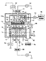
図1に、本発明の第1の実施例におけるプラズマエッチング装置の構成を示す。このプラズマエッチング装置は、容量結合型平行平板プラズマエッチング装置として構成されており、たとえば表面がアルマイト処理(陽極酸化処理)されたアルミニウムからなる円筒形のチャンバ(処理容器)10を有している。チャンバ10は保安接地されている。
FIG. 1 shows the configuration of a plasma etching apparatus in the first embodiment of the present invention. This plasma etching apparatus is configured as a capacitively coupled parallel plate plasma etching apparatus, and has, for example, a cylindrical chamber (processing vessel) 10 made of aluminum whose surface is anodized (anodized). The
チャンバ10の底部には、セラミックなどの絶縁板12を介して円柱状のサセプタ支持台14が配置され、このサセプタ支持台14の上にたとえばアルミニウムからなるサセプタ16が設けられている。サセプタ16は下部電極を構成し、この上に被処理基板としてたとえば半導体ウエハWが載置される。
A
サセプタ16の上面には半導体ウエハWを静電吸着力で保持するための静電チャック18が設けられている。この静電チャック18は導電膜からなる電極20を一対の絶縁層または絶縁シートの間に挟み込んだものであり、電極20には直流電源22が電気的に接続されている。直流電源22からの直流電圧により、半導体ウエハWがクーロン力で静電チャック18に吸着保持されるようになっている。静電チャック18の周囲でサセプタ16の上面には、エッチングの均一性を向上させるためのたとえばシリコンからなるフォーカスリング24が配置されている。サセプタ16およびサセプタ支持台14の側面にはたとえば石英からなる円筒状の内壁部材26が貼り付けられている。
An
サセプタ支持台14の内部には、たとえば円周方向に延在する冷媒室28が設けられている。この冷媒室28には、外付けのチラーユニット(図示せず)より配管30a,30bを介して所定温度の冷媒たとえば冷却水が循環供給される。冷媒の温度によってサセプタ16上の半導体ウエハWの処理温度を制御できる。
Inside the
さらに、伝熱ガス供給機構(図示せず)からの伝熱ガスたとえばHeガスがガス供給ライン32を介して静電チャック18の上面と半導体ウエハWの裏面との間に供給される。
Further, a heat transfer gas such as He gas from a heat transfer gas supply mechanism (not shown) is supplied between the upper surface of the
サセプタ16の上方には、このサセプタと平行に対向して上部電極34が設けられている。両電極16,34の間の空間はプラズマ生成空間である。上部電極34は、サセプタ(下部電極)16上の半導体ウエハWと対向してプラズマ生成空間と接する面つまり対向面を形成する。上部電極34は、サセプタ16と所望の間隔を置いて対向配置されているリング形状またはドーナツ形状の外側(outer)上部電極36と、この外側上部電極36の半径方向内側に絶縁して配置されている円板形状の内側(inner)上部電極38とで構成される。これら外側上部電極36と内側上部電極38とは、プラズマ生成に関して、前者(36)が主で、後者(38)が補助の関係を有している。
An
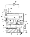
図2に、この実施例におけるプラズマエッチング装置の要部の構成を示す。図2に明示するように、外側上部電極36と内側上部電極38との間にはたとえば0.25〜2.0mmの環状ギャップ(隙間)が形成され、このギャップにたとえば石英からなる誘電体40が設けられる。また、このギャップにセラミック96を設けることもできる。この誘電体40を挟んで両電極36,38の間にコンデンサが形成される。このコンデンサのキャパシタンスC40は、ギャップのサイズと誘電体40の誘電率に応じて所望の値に選定または調整される。外側上部電極36とチャンバ10の側壁との間には、たとえばアルミナ(Al2O3)からなるリング形状の絶縁性遮蔽部材42が気密に取り付けられている。
FIG. 2 shows the configuration of the main part of the plasma etching apparatus in this embodiment. As clearly shown in FIG. 2, an annular gap (gap) of, for example, 0.25 to 2.0 mm is formed between the outer
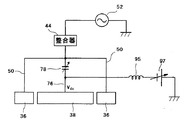
外側上部電極36は、ジュール熱の少ない低抵抗の導電体または半導体たとえばシリコンで構成されるのが好ましい。外側上部電極36には、整合器44、上部給電棒46、コネクタ48および給電筒50を介して第1の高周波電源52が電気的に接続されている。第1の高周波電源52は、13.5MHz以上の周波数たとえば60MHzの高周波電圧を出力する。整合器44は、高周波電源52の内部(または出力)インピーダンスに負荷インピーダンスを整合させるためのもので、チャンバ10内にプラズマが生成されている時に高周波電源50の出力インピーダンスと負荷インピーダンスが見かけ上一致するように機能する。整合器44の出力端子は上部給電棒46の上端に接続されている。
The outer
給電筒50は、円筒状または円錐状あるいはそれらに近い形状の導電板たとえばアルミニウム板または銅板からなり、下端が周回方向で連続的に外側上部電極36に接続され、上端がコネクタ48によって上部給電棒46の下端部に電気的に接続されている。給電筒50の外側では、チャンバ10の側壁が上部電極34の高さ位置よりも上方に延びて円筒状の接地導体10aを構成している。この円筒状接地導体10aの上端部は筒状の絶縁部材54により上部給電棒46から電気的に絶縁されている。かかる構成においては、コネクタ48からみた負荷回路において、給電筒50および外側上部電極36と円筒状接地導体10aとで前者(36,50)を導波路とする同軸線路が形成される。
The
再び図1において、内側上部電極38は、多数のガス通気孔56aを有するたとえばSi、SiCなどの半導体材料からなる電極板56と、この電極板56を着脱可能に支持する導電材料たとえば表面がアルマイト処理されたアルミニウムからなる電極支持体58とを有する。電極支持体58の内部には、たとえばOリングからなる環状隔壁部材60で分割された2つのガス導入室つまり中心ガス導入室62と周辺ガス導入室64とが設けられている。中心ガス導入室62とその下面に設けられている多数のガス噴出孔56aとで中心シャワーヘッドが構成され、周辺ガス導入室64とその下面に設けられている多数のガス噴出孔56aとで周辺シャワーヘッドが構成されている。
In FIG. 1 again, the inner
これらのガス導入室62,64には、共通の処理ガス供給源66からの処理ガスが所望の流量比で供給されるようになっている。より詳細には、処理ガス供給源66からのガス供給管68が途中で2つに分岐してガス導入室62,64に接続され、それぞれの分岐管68a,68bに流量制御弁70a,70bが設けられている。処理ガス供給源66からガス導入室62,64までの流路のコンダクタンスは等しいので、流量制御弁70a,70bの調整により、両ガス導入室62,64に供給する処理ガスの流量比を任意に調整できるようになっている。なお、ガス供給管68にはマスフローコントローラ(MFC)72および開閉バルブ74が設けられている。このように、中心ガス導入室62と周辺ガス導入室64とに導入する処理ガスの流量比を調整することで、中心ガス導入室62に対応する電極中心部のガス通気孔56aつまり中心シャワーヘッドより噴出されるガスの流量FCと周辺ガス導入室64に対応する電極周辺部のガス通気孔56aつまり周辺シャワーヘッドより噴出されるガスの流量F E との比率(FC/FE)を任意に調整できるようになっている。なお、中心シャワーヘッドおよび周辺シャワーヘッドよりそれぞれ噴出させる処理ガスの単位面積当たりの流量を異ならせることも可能である。さらに、中心シャワーヘッドおよび周辺シャワーヘッドよりそれぞれ噴出させる処理ガスのガス種またはガス混合比を独立または別個に選定することも可能である。
A processing gas from a common processing
内側上部電極38の電極支持体58には、整合器44、上部給電棒46、コネクタ48および下部給電筒76を介して第1の高周波電源52が電気的に接続されている。下部給電筒76の途中には、キャパシタンスを可変調整できる可変コンデンサ78が設けられている。
The first high-
図示省略するが、外側上部電極36および内側上部電極38にも適当な冷媒室または冷却ジャケット(図示せず)を設けて、外部のチラーユニットにより冷媒を介して電極の温度を制御できるように構成してもよい。
Although not shown, the outer
チャンバ10の底部には排気口80が設けられ、この排気口80に排気管82を介して排気装置84が接続されている。排気装置84は、ターボ分子ポンプなどの真空ポンプを有しており、チャンバ10内のプラズマ処理空間を所望の真空度まで減圧できるようになっている。また、チャンバ10の側壁には半導体ウエハWの搬入出口を開閉するゲートバルブ86が取り付けられている。
An
この実施例のプラズマエッチング装置では、下部電極としてのサセプタ16に整合器88を介して第2の高周波電源90が電気的に接続されている。この第2の高周波電源90は、2〜27MHzの範囲内の周波数、たとえば2MHzの高周波電圧を出力する。整合器88は、高周波電源90の内部(または出力)インピーダンスに負荷インピーダンスを整合させるためのもので、チャンバ10内にプラズマが生成されている時に高周波電源90の内部インピーダンスと負荷インピーダンスが見かけ上一致するように機能する。
In the plasma etching apparatus of this embodiment, the second high
内側上部電極38には、第1の高周波電源52からの高周波(60MHz)を通さずに第2の高周波電源98からの高周波(2MHz)をグランドへ通すためのローパスフィルタ(LPF)92が電気的に接続されている。このローパスフィルタ(LPF)92は、好適にはLRフィルタまたはLCフィルタで構成されてよいが、1本の導線だけでも第1の高周波電源52からの高周波(60MHz)に対しては十分大きなリアクタンスを与えることができるので、それで済ますこともできる。一方、サセプタ16には、第1の高周波電源52からの高周波(60MHz)をグランドへ通すためのハイパスフィルタ(HPF)94が電気的に接続されている。
The inner
このプラズマエッチング装置において、エッチングを行なうには、先ずゲートバルブ86を開状態にして加工対象の半導体ウエハWをチャンバ10内に搬入して、サセプタ16の上に載置する。そして、処理ガス供給源66よりエッチングガス(一般に混合ガス)を所定の流量および流量比でガス導入室62,64に導入し、排気装置84によりチャンバ10内の圧力つまりエッチング圧力を設定値(たとえば数mTorr〜1Torrの範囲内)とする。さらに、第1の高周波電源52よりプラズマ生成用の高周波(60MHz)を所定のパワーで上部電極34(36,38)に印加するとともに、第2の高周波電源90より高周波(2MHz)を所定のパワーでサセプタ16に印加する。また、直流電源22より直流電圧を静電チャック18の電極20に印加して、半導体ウエハWをサセプタ16に固定する。内側上部電極38のガス通気孔56aより吐出されたエッチングガスは上部電極34(36,38)とサセプタ16間のグロー放電中でプラズマ化し、このプラズマで生成されるラジカルやイオンによって半導体ウエハWの被処理面がエッチングされる。
In order to perform etching in this plasma etching apparatus, first, the
このプラズマエッチング装置では、上部電極34に対して高い周波数領域(イオンが動けない5〜10MHz以上)の高周波を印加することにより、プラズマを好ましい解離状態で高密度化し、より低圧の条件下でも高密度プラズマを形成することができる。
In this plasma etching apparatus, by applying a high frequency in a high frequency region (5 to 10 MHz or more at which ions cannot move) to the
また、上部電極34において、半導体ウエハWと真正面に対向する内側上部電極38をシャワーヘッド兼用型とし、中心シャワーヘッド(62,56a)と周辺シャワーヘッド(64,56a)とでガス吐出流量の比率を任意に調整できるので、ガス分子またはラジカル密度の空間分布を径方向で制御し、ラジカルベースによるエッチング特性の空間的な分布特性を任意に制御することもできる。
In the
一方、上部電極34においては、後述するように、プラズマ生成のための高周波電極として外側上部電極36を主、内側上部電極38を副とし、両高周波電極36,38より電極直下の電子に与える電界強度の比率を調整可能にしているので、プラズマ密度の空間分布を径方向で制御し、反応性イオンエッチングの空間的な特性を任意かつ精細に制御することができる。
On the other hand, in the
ここで、重要なことは、外側上部電極36と内側上部電極38との間で電界強度または投入電力の比率を可変することによって行なわれるプラズマ密度空間分布の制御が、中心シャワーヘッド(62,56a)と周辺シャワーヘッド(64,56a)との間で処理ガスの流量やガス密度またはガス混合比の比率を可変することによって行なわれるラジカル密度空間分布の制御に実質的な影響を及ぼさないことである。つまり、中心シャワーヘッド(62,56a)と周辺シャワーヘッド(64,56a)より噴出される処理ガスの解離が内側上部電極38直下のエリア内で行なわれるため、内側上部電極38と外側上部電極36との間で電界強度のバランスを変えても、内側上部電極38内(同一エリア内)の中心シャワーヘッド(62,56a)と周辺シャワーヘッド(64,56a)との間のラジカル生成量ないし密度のバランスにはさほど影響しない。このように、プラズマ密度の空間分布とラジカル密度の空間分布とを実質上独立に制御することができる。
Here, it is important that the control of the plasma density spatial distribution performed by varying the ratio of the electric field strength or the input power between the outer
また、このプラズマエッチング装置は、外側上部電極36の直下でプラズマの大部分ないし過半を生成して内側上部電極38の直下に拡散させる方式である。この方式によると、シャワーヘッドを兼ねる内側上部電極38においては、プラズマのイオンから受けるアタックが少ないため交換部品である電極板56のガス吐出口56aのスパッタ進行度を効果的に抑制し、電極板56の寿命を大幅に延ばすことができる。一方、外側上部電極36は、電界の集中するガス吐出口を有してはいないため、イオンのアタックは少なく、内側上部電極38の代わりに電極寿命が短くなるようなことはない。
This plasma etching apparatus is a system in which most or most of the plasma is generated immediately below the outer
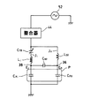
図2は、先に述べたように、このプラズマエッチング装置の要部(特に、プラズマ生成手段を構成する要部)の構成を示している。図中、内側上部電極38のシャワーヘッド部(56a、62,64)の構造を省略している。図3に、プラズマ生成手段の要部の等価回路を示す。この等価回路では各部の抵抗を省略している。
FIG. 2 shows the configuration of the main part of this plasma etching apparatus (particularly, the main part constituting the plasma generating means) as described above. In the drawing, the structure of the shower head portion (56a, 62, 64) of the inner
この実施例では、上記のように、コネクタ48からみた負荷回路において、外側上部電極36および給電筒50と円筒状接地導体10aとで前者(36,50)を導波路Joとする同軸線路が形成される。ここで、給電筒50の半径(外径)をao、円筒状接地導体10aの半径をbとすると、この同軸線路の特性インピーダンスまたはインダクタンスLoは下記の式(1)で近似できる。
Lo=K・In(b/ao) ‥‥‥(1)
ただし、Kは導電路の移動度および誘電率で決まる定数である。
In this embodiment, as described above, in the load circuit viewed from the
Lo = K · In (b / a o ) (1)
However, K is a constant determined by the mobility and dielectric constant of the conductive path.
一方、コネクタ48からみた負荷回路において、下部給電棒76と円筒状接地導体10aとの間でも前者(76)を導波路Jiとする同軸線路が形成される。内側上部電極38も下部給電棒76の延長上にあるが、直径が違いすぎており、下部給電棒76のインピーダンスが支配的になる。ここで、下部給電棒76の半径(外径)をaiとすると、この同軸線路の特性インピーダンスまたはインダクタンスLiは下記の式(2)で近似できる。
Li=K・In(b/ai) ‥‥‥(2)
On the other hand, in the load circuit viewed from the
Li = K · In (b / a i ) (2)
上記の式(1),(2)より理解されるように、内側上部電極38に高周波を伝える内側導波路Jiは従来一般のRFシステムと同様のインダクタンスLiを与えるのに対して、外側上部電極36に高周波を伝える外側導波路Joは径が大きい分だけ著しく小さなインダクタンスLoを与えることができる。これにより、整合器44からみてコネクタ48より先の負荷回路では、低インピーダンスの外側導波路Joで高周波が伝播しやすく(電圧降下が小さく)、外側上部電極36に多めの高周波電力Poを供給して、外側上部電極36の下面(プラズマ接触面)に強い電界強度Eoを得ることができる。一方、高インピーダンスの内側導波路Jiでは高周波が伝播しにくく(電圧降下が大きく)、内側上部電極38に外側上部電極36に供給される高周波電力Poよりも小さい高周波電力Piを供給して、内側上部電極38の下面(プラズマ接触面)に得られる電界強度Eiを外側上部電極36側の電界強度Eoよりも小さくすることができる。
As understood from the above formulas (1) and (2), the inner waveguide Ji for transmitting a high frequency to the inner
このように、上部電極34では、外側上部電極36の直下で相対的に強い電界Eoで電子を加速させると同時に、内側上部電極38の直下では相対的に弱い電界Eiで電子を加速させることとなり、これによって外側上部電極36の直下でプラズマPの大部分ないし過半が生成され、内側上部電極38の直下では補助的にプラズマPの一部が生成される。そして、外側上部電極36の直下で生成された高密度のプラズマが径方向の内側と外側に拡散することにより、上部電極34とサセプタ16との間のプラズマ処理空間においてプラズマ密度が径方向で均される。
As described above, in the
ところで、外側上部電極36および給電筒50と円筒状接地導体10aとで形成される同軸線路における最大伝送電力Pmaxは、給電筒50の半径aoと円筒状接地導体10aの半径bとに依存し、下記の式(3)で与えられる。
Pmax/Eo 2 max=ao 2[In(b/ao)]2/2Zo ‥‥‥(3)
ここで、Zoは整合器44側からみた当該同軸線路の入力インピーダンスであり、EomaxはRF伝送系の最大電界強度である。
By the way, the maximum transmission power P max in the coaxial line formed by the outer
P max / E o 2 max = a o 2 [In (b / a o )] 2 / 2Z o (3)
Here, Z o is the input impedance of the coaxial line viewed from the matching
上記の式(3)において、最大伝送電力Pmaxは(b/ao)≒1.65で極大値となる。このことから、外側導波路Joの電力伝送効率を向上させるには、給電筒50の径サイズに対して円筒状接地導体10aの径サイズの比(b/ao)が約1.65となるように構成する(給電筒50および/または円筒状接地導体10aの径サイズを選定する)のが最も好ましく、少なくとも1.2〜2.0の範囲内に入るように構成するのが好ましく、1.5〜1.7の範囲内に入るように構成するのがさらに好ましい。
In the above equation (3), the maximum transmission power P max becomes a maximum value when (b / a o ) ≈1.65. From this, in order to improve the power transmission efficiency of the outer waveguide Jo, the ratio (b / a o ) of the diameter size of the
この実施例では、プラズマ密度の空間分布を任意かつ精細に制御するために、外側上部電極36直下の外側電界強度Eo(または外側上部電極36側への投入電力Po)と内側上部電極38直下の内側電界強度Ei(または内側上部電極38側への投入電力Pi)との比率つまりバランスを調整するための手段として、下部給電棒76の途中に可変コンデンサ78を挿入している。この可変コンデンサ78のキャパシタンスC78を変えることにより、内側導波路Jiのインピーダンスまたはリアクタンスを増減させ、外側導波路Joの電圧降下と内側導波路Jiの電圧降下との相対比率を変えることができ、ひいては外側電界強度Eo(外側投入電力Po)と内側電界強度Ei(内側投入電力Pi)との比率を調整することができる。
In this embodiment, in order to arbitrarily and finely control the spatial distribution of the plasma density, the outer electric field intensity Eo directly below the outer upper electrode 36 (or the input power Po to the outer
なお、プラズマの電位降下を与えるイオンシースのインピーダンスは一般に容量性である。図3の等価回路では、外側上部電極36直下におけるシースインピーダンスのキャパシタンスをCpo、内側上部電極38直下におけるシースインピーダンスのキャパシタンスをCpiと仮定(擬制)している。また、外側上部電極36と内側上部電極38との間に形成されるコンデンサのキャパシタンスC40は、可変コンデンサ78のキャパシタンスC78と組み合わさって上記のような外側電界強度Eo(外側投入電力Po)と内側電界強度Ei(内側投入電力Pi)とのバランスを左右するものであり、可変コンデンサ78による電界強度(投入電力)バランス調整機能を最適化できるような値に選定または調整されてよい。
It should be noted that the impedance of the ion sheath that gives a plasma potential drop is generally capacitive. In the equivalent circuit of FIG. 3, the capacitance of the sheath impedance immediately below the outer
ここで、図4および図5に、この実施例の可変コンデンサ78による電界強度バランス調整機能の検証例(シミュレーションデータ)を示す。図4は、可変コンデンサ78のキャパシタンスC78をパラメータにして電極の径方向における電界強度(相対値)の分布特性を示す。図5は、可変コンデンサ78のキャパシタンスC78を変えたときの外側電界強度Eoと内側電界強度Eiとの相対比率を示す。なお、このシミュレーションでは、半導体ウエハWの口径を200mmとし、円板形状の内側上部電極38の半径を100mm、リング形状の外側上部電極36の内側半径および外側半径をそれぞれ101mm、141mmに選んでいる。この場合、半導体ウエハWの面積(314cm2)に対して、内側上部電極38の面積は314cm2でウエハWと同じであり、外側上部電極36の面積は304cm2でウエハWよりも幾らか小さい。概して、外側上部電極36の面積は内側上部電極38の面積の約1/4倍〜約1倍に選ばれるのが好ましい。
Here, FIGS. 4 and 5 show verification examples (simulation data) of the electric field strength balance adjustment function by the
図4に示すように、外側上部電極36直下の外側電界強度Eoの方が内側上部電極38直下の内側電界強度Eiよりも大きく、両電極36,38の境界付近で電界強度に大きな段差が生じる。特に、外側上部電極36直下の外側電界強度Eoは内側上部電極38との境界付近で最大になり、半径方向の外側にいくほど低くなる傾向があることがわかる。この例では、図5に示すように、可変コンデンサ78のキャパシタンスC78を180〜350pFの範囲内で変えると、電界強度Ei,Eoの比率Ei/Eoを約10%〜40%の範囲内で連続的に制御できることがわかる。なお、C78=125〜180pFは負荷回路が共振する領域であり、制御不能となっている。基本的に、安定領域では、可変コンデンサ78のキャパシタンスC78を大きくするほど、内側導波路Jiのリアクタンスを減少させて、内側上部電極38直下の内側電界強度Eiを相対的に増大させ、外側電界強度Eoと内側電界強度Eiの比率Ei/Eoを高くする方向に制御できる。
As shown in FIG. 4, the outer electric field intensity Eo directly below the outer
この実施例においては、給電筒50により構成される外側導波路Joのリアクタンスを著しく小さくできるため、整合器44の出力端子からみた負荷回路のインピーダンスのリアクタンスを容量性の負値にすることができる。このことは、整合器44の出力端子から容量性のイオンシースに至るまでの導波路において、リアクタンスが誘電性の正値から負値に極性反転するような共振ポイントが存在しないことを意味する。共振ポイントの発生を回避することで、共振電流の発生を回避し、高周波エネルギーの損失を低減できるとともにプラズマ密度分布制御の安定性を確保できる。
In this embodiment, since the reactance of the outer waveguide Jo constituted by the
図6A、図6Bおよび図7A、図7Bに、この実施例のプラズマエッチング装置において得られる電子密度分布特性およびエッチングレート分布特性の一例(実験データ)を示す。図4および図5の電界強度分布特性と同様に可変コンデンサ78のキャパシタンスC78をパラメータにして、プラズマ吸収プローブ(PAP)を用いて径方向の各位置における電子密度を測定するとともに、半導体ウエハ上のシリコン酸化膜をエッチングして径方向の各ウエハ位置におけるエッチング速度を測定した。この実験でも、内側上部電極38の半径を100mm、外側上部電極36の内側半径および外側半径をそれぞれ101mm、141mmに選んでいる。主なエッッチング条件は下記のとおりである。
ウエハ口径=200mm
チャンバ内の圧力=15mTorr、
温度(上部電極/チャンバ側壁/下部電極)=60/50/20゜C、
電熱ガス(Heガス)供給圧力(センター部/エッジ部)=15/25Torr、
上部及び下部電極間距離=50mm
プロセスガス(C5F8/Ar/O2)≒流量20/380/20sccm
高周波電力(60MHz/2MHz)≒2200W/1500W(C78=500pF,1000pF),1800W(C78=120pF)
FIGS. 6A, 6B, 7A, and 7B show examples (experimental data) of electron density distribution characteristics and etching rate distribution characteristics obtained in the plasma etching apparatus of this embodiment. Similar to the electric field strength distribution characteristics of FIGS. 4 and 5, the capacitance C 78 of the
Wafer diameter = 200 mm
Pressure in chamber = 15 mTorr,
Temperature (upper electrode / chamber sidewall / lower electrode) = 60/50/20 ° C.
Electric heating gas (He gas) supply pressure (center portion / edge portion) = 15/25 Torr,
Distance between upper and lower electrodes = 50 mm
Process gas (C 5 F 8 / Ar / O 2 ) ≈
High frequency power (60 MHz / 2 MHz) ≈2200 W / 1500 W (C 78 = 500 pF, 1000 pF), 1800 W (C 78 = 120 pF)
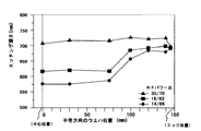
図6Aおよび図6Bにおいて、可変コンデンサ78のキャパシタンスC78を120pFに選んだときは、外側電界強度Eoと内側電界強度Eiの比率Ei/Eoを高めに選んだ場合であり、この場合は、電極中心付近が最大で、径方向外側にいくほど単調に減少するような電子密度つまりプラズマ密度の分布特性を得ることができる。これは、主プラズマ生成部である外側上部電極36の直下におけるプラズマ生成率と副プラズマ生成部である内側上部電極38の直下におけるプラズマ生成率との差をプラズマの拡散率が上回って、全方向から集まる中心部のプラズマ密度が周りよりも相対的に高くなるものと考えられる。
6A and 6B, when the capacitance C 78 of the
一方、キャパシタンスC78を1000pFに選んだときは、外側電界強度Eoと内側電界強度Eiの比率Ei/Eoを低めに選んだ場合であり、この場合は、径方向でウエハの内側よりも外側の位置(中心から140mmの位置付近)で電子密度を極大化させ、ウエハの内側(0〜100mm)ではほぼ均一な電子密度分布を得ることができる。これは、内側上部電極38の直下におけるプラズマ生成率の増大によって半径方向外側への拡散が強まるためと考えられる。いずれにしても、可変コンデンサ78のキャパシタンスC78を適当な範囲内で細かく可変調整することにより、電子密度つまりプラズマ密度の空間分布特性を自在かつ精細に制御できることがわかる。
On the other hand, when the capacitance C 78 is selected to be 1000 pF, the ratio Ei / Eo between the outer electric field strength Eo and the inner electric field strength Ei is selected to be lower. In this case, the outer diameter is larger than the inner side of the wafer. The electron density can be maximized at a position (near the position of 140 mm from the center), and a substantially uniform electron density distribution can be obtained inside the wafer (0 to 100 mm). This is presumably because diffusion to the outside in the radial direction is strengthened by an increase in the plasma generation rate immediately below the inner
また、下部電極16に高周波バイアス(2MHz)を印加した場合(図6A)は、印加しない場合(図6B)と比較して、各位置の電子密度がある程度増大することと、分布パターンはほとんど変わらないことがわかる。
Further, when a high frequency bias (2 MHz) is applied to the lower electrode 16 (FIG. 6A), the electron density at each position increases to some extent and the distribution pattern is almost the same as when not applied (FIG. 6B). I understand that there is no .
図7Aおよび図7Bの実験データによれば、可変コンデンサ78のキャパシタンスC78を可変調整することで、図6Aおよび図6Bの電子密度空間分布特性に対応するパターンのエッチングレート空間分布特性が得られることがわかる。すなわち、可変コンデンサ78のキャパシタンスC78を適当な範囲内で細かく可変調整することにより、ウエハ面内のエッチングレート空間分布特性も自在かつ精細に制御可能できることがわかる。
According to the experimental data of FIGS. 7A and 7B, the etching rate spatial distribution characteristics corresponding to the electron density spatial distribution characteristics of FIGS. 6A and 6B can be obtained by variably adjusting the capacitance C78 of the
また、この実施例のプラズマエッチング装置では、上記したように内側上部電極36のシャワーヘッド機構において中心部と外周部とでガス吐出流量の比率を可変調整する機能により、ラジカルベースでエッチングレート空間分布特性の制御を併せて行うことも可能である。
In the plasma etching apparatus of this embodiment, as described above, in the shower head mechanism of the inner
図8に、本発明の第2の実施例におけるプラズマエッチング装置の構成を示す。図中、上記した第1実施例の装置(図1)におけるものと同様の構成または機能を有する部分には同一の符号を付してある。 FIG. 8 shows the configuration of the plasma etching apparatus in the second embodiment of the present invention. In the figure, parts having the same configuration or function as those in the apparatus of the first embodiment (FIG. 1) are given the same reference numerals.
この第2の実施例における特徴の一つは、高周波電源52からの高周波を外側上部電極36に伝送するための伝送路つまり給電筒50に鋳物を用いる構成である。この鋳物の材質は導電性と加工性に優れた金属が好ましく、たとえばアルミニウムでよい。鋳物の利点の一つはコストが低いことであり、板材製のものと比べて1/7以下のコストに抑えることができる。別の利点として、鋳物は一体化が容易で、RF接面を低減できるため、RF損失を少なくすることができる。
One of the features of the second embodiment is that the casting is used for the transmission path for transmitting the high frequency from the high
さらに、給電筒50を鋳物で構成しても、高周波伝送効率が低下することはない。すなわち、図9A,図9Bおよび図10A,図10Bの実験データに示すように、給電筒50を板材で構成しても鋳物で構成しても、エッチングレートは殆ど違わないことが確認されている。なお、図9Aおよび図9Bはシリコン酸化膜(SiO2)に係るエッチングレートの空間分布特性を示し、図10Aおよび図10Bはフォトレジスト(PR)に係るエッチングレートの空間分布特性を示す。この検証例における主なエッチング条件は下記のとおりである。
ウエハ口径=300mm
チャンバ内の圧力=25mTorr
温度(上部電極/チャンバ側壁/下部電極)=60/60/20゜C
伝熱ガス(Heガス)供給圧力(センター部/エッジ部)=15/40Torr
上部及び下部電極間距離=45mm
プロセスガス(C5F8/Ar/O2)≒流量30/750/50sccm
高周波電力(60MHz/2MHz)≒3300W/3800W
測定時間=120秒
Furthermore, even if the
Wafer diameter = 300mm
Pressure in chamber = 25mTorr
Temperature (upper electrode / chamber sidewall / lower electrode) = 60/60/20 ° C
Heat transfer gas (He gas) supply pressure (center / edge) = 15/40 Torr
Distance between upper and lower electrodes = 45mm
Process gas (C 5 F 8 / Ar / O 2 ) ≈
High frequency power (60MHz / 2MHz) ≒ 3300W / 3800W
Measurement time = 120 seconds
この第2の実施例における第2の特徴は、給電筒50内で給電棒76の回りにリング状の導体部材100を設ける構成である。この導体部材100の主たる役目は、以下に述べるように、給電棒76回りのインダクタンスを小さくして、可変コンデンサ78による外側/内側投入電力バランス調整機能のレンジを改善することにある。
The second feature of the second embodiment is a configuration in which a ring-shaped
このプラズマ処理装置では、上記のように、可変コンデンサ78のキャパシタンスC78を変えることで、外側上部電極36に対する投入電力Poと内側上部電極38に対する投入電力Piの比率を任意に調節することができる。一般に、可変コンデンサ78におけるキャパシタンスC78の可変調整は、ステップモータ等を用いてステップ的に行なわれる。このキャパシタンス可変調整では、上記のように制御不能な共振領域(図5では125pF<C78<180pFの領域)を避ける必要があり、上記第1の実施例における実験検証例(図6A,図6B,図7A,図7B)では主に共振領域より右側の安定領域(C78≧180pF)を使用した。しかしながら、右側安定領域は内側投入電力Piの比率を上げるのに限界があるうえ、電力の損失も大きいという側面がある。この点、図4および図5からも明らかなように共振領域より左側の領域(C78≦125pF)は内側投入電力Piの比率を上げるのに有利であるうえ、電力損失も少ないという利点がある。ただし、共振領域より左側の領域では内側投入電力Piの比率を上げるほど共振領域に近づくため、図11のAのような変化率(傾斜)の大きな特性曲線の下では共振領域手前での微調整が非常に難しくなるという側面がある。
In this plasma processing apparatus, as described above, by changing the capacitance C 78 of the
これを解決するには、図11のBで示すようにキャパシタンス−内側投入電力比率特性曲線において共振領域より左側の領域の変化率(傾斜)を小さくして調整レンジを広げることが有効である。そして、図11のBのような傾斜の緩いブロードの特性曲線を得るには、以下に述べるように給電棒76回りのインダクタンスLiを小さくするのが有効である。
In order to solve this, it is effective to reduce the rate of change (inclination) in the region on the left side of the resonance region in the capacitance-inside input power ratio characteristic curve as shown in FIG. In order to obtain a broad characteristic curve having a gentle slope as shown in FIG. 11B, it is effective to reduce the inductance L i around the
すなわち、このプラズマエッチング装置におけるプラズマ生成用の高周波給電回路を図12に示すような等価回路で表すと、給電棒76回りのリアクタンスωLiはコンデンサ78のリアクタンス1/ωC78よりも常に大きい絶対値をとることから、内側導波路Jiの合成リアクタンスXは常に誘導性であり、X=ωLaと表すことができる。この見かけ上のインダクタンスLaとキャパシタンスC40とで形成される並列回路が共振状態になるときは、インダクタンスLaのサセプタンス1/ωLaとキャパシタンスC40のサセプタンスωC40とが相殺して零になるとき、つまり1/ωLa=1/(ωLi−1/ωC78)=ωC40が成立するときである。ここで、Liを小さくするほど、上記共振条件を成立させるC78の値が大きくなり、図11のBに示すような共振領域の手前で傾斜の緩やかなブロードの特性曲線が得られる。なお、図12の等価回路では、説明を簡単にするために、外側導波路JoのインダクタンスLoを省いている。この等価回路にインダクタンスLoが入っていても原理は同じである。
That is, when the high-frequency power supply circuit for generating plasma in this plasma etching apparatus is represented by an equivalent circuit as shown in FIG. 12, the reactance ωL i around the
図13に、この実施例における導体部材100の作用を示す。給電棒76に時間的に変化する電流Iが流れるとき、給電棒76の回りにはループ状の磁束Bが生成されるとともに、電磁誘導によって導体部材100の内部では磁束Bと鎖交する誘導電流iが流れる。そうすると、この誘導電流iによって導体部材100の内外にループ状の磁束bが生成され、導体部材100の内部では磁束bの分だけ磁束Bが相殺される。こうして、給電棒76の回りに導体部材100を設けることで、給電棒76回りの正味の磁束発生量を低減してインダクタンスLiを小さくすることができる。
FIG. 13 shows the operation of the
導体部材100の外観構造は、周回方向に連続した単一のリング形体が好ましいが、複数の導体部材を周回方向に並べて配置する構造であってもよい。また、導体部材100の内部構造は、図13に示すようなリング状の空洞を有する中空体でもよいが、図8に示すような内部の埋まったブロック体構造の方がより大きなインダクタンス低減効果を得ることができる。導体部材100の容積は大きいほど好ましく、理想的には給電筒50内側の空間を埋め尽くすのが最も好ましい。実用的には、給電筒50と外側上部電極36とで囲まれる空間の1/10〜1/3を導体部材100で埋めるのが好ましい。導体部材100の材質は任意の導電材料でよく、たとえばアルミニウムの鋳物でもよい。なお、導体部材100は、付近の導体すなわち給電棒76や内側上部電極38等と電気的に絶縁された状態で配置される。
The appearance structure of the
図14に、この実施例における導体部材100による上記ブロード効果の実証例を実験データで示す。図14において、特性曲線B'はこの実施例の装置構造で得られたものであり、特性曲線A'は導体部材100を設けない装置構造で得られたものである。これらの特性曲線A',B'はそれぞれ図11の特性曲線A,Bを上下にひっくり返したものに対応する。すなわち、この種の平行平板型プラズマ装置では、上部電極34の中心部への投入電力(内側投入電力Pi)の比率を上げるほど、サセプタ16側では基板W近傍のプラズマ密度が高くなり、これによって(プラズマ密度と反比例する)サセプタ16側のバイアス周波数のVppが低くなるという関係がある。この関係から、可変コンデンサ78のバリコンステップ値(キャパシタンスC78の値に比例する制御量)を可変して各ステップ値で得られるV pp の測定値をプロットして得られる特性曲線A',B'(図14)は、図11の特性曲線A,Bを上下にひっくり返したものにそれぞれ対応する。図14の特性曲線B' から実証されるように、この実施例によれば、給電棒76の回りに導体部材100を設けることで、可変コンデンサ78による外側/内側投入電力バランス調整において内側投入電力投入電力Piの比率を共振領域の手前で可及的に高い値まで安定かつ精細に制御することができる。
In FIG. 14, the demonstration example of the said broad effect by the
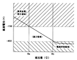
この実施例における第3の特徴は、内側上部電極38とグランド電位との間に接続されるローパスフィルタ92に係るものである。図15Aに示すように、この実施例におけるローパスフィルタ92は、可変抵抗器93とコイル95とを直列接続してなり、プラズマ生成用の高周波(60MHz)を通さず、バイアス用の高周波(2MHz)以下の交流周波数と直流とを通すように構成されている。このローパスフィルタ92によれば、可変抵抗器93の抵抗値R93を可変調整することによって、内側上部電極38の直流電位または自己バイアス電圧Vdcを調整できる。
The third feature of this embodiment relates to the low-
より詳細には、図16に示すように、抵抗器93の抵抗値R93を小さくするほど、抵抗器93の電圧降下が小さくなり、負の直流電位Vdcは上昇する(グランド電位に近づく)。逆に、抵抗器93の抵抗値R93を大きくするほど、抵抗器93の電圧降下が大きくなり、直流電位Vdcは下がる。もっとも、直流電位Vdcが高くなりすぎると(通常は−150Vよりも高くなると)、プラズマポテンシャルが上昇して、異常放電またはアーキングが発生する。一方、直流電位Vdcが低くなりすぎると(通常は−450Vよりも低くなると)、内側上部電極38へのイオンのアタックが強くなって電極の消耗が早まる。別な見方をすれば、図17に示すように、直流電位Vdcには上記のような異常放電および電極消耗のいずれも防止ないし抑制できる適性範囲(−450V〜−150V)があり、この適性範囲に対応する抵抗値R93の範囲(Ra〜Rb)が存在する。したがって、抵抗器93側から抵抗値R93を上記範囲(Ra〜Rb)内に選定または調整することで、直流電位Vdcを上記適性範囲(−450V〜−150V)内に調整することができる。また、上部電極34(外側上部電極36および内側上部電極38)全体に印加する高周波電力の値によっても抵抗値R93の適性範囲(Ra〜Rb)が変わる。一例として、3000Wの高周波パワーに対して、下限抵抗値Ra=約1MΩの実験結果が得られている。
More specifically, as shown in FIG. 16, as the resistance value R 93 of the resistor 93 is decreased, the voltage drop of the
また、図15Bに示すように、内側上部電極38を可変直流電源97を介してグランドに接地し、直流電位Vdcを電源電圧によって直接的に制御することも可能である。可変直流電源97は、バイポーラ電源で構成するのが好ましい。
Further, as shown in FIG. 15B, the inner
この第2の実施例における第4の特徴は、上部電極34において、外側上部電極36の下面を内側上部電極38の下面よりも下方つまりサセプタ16側に突出させる構成である。図18に、この特徴部分の構成を拡大して示す。図示の例では、外側上部電極36を上部電極部材36Aと下部電極部材36Bとからなる上下2分割構造としている。本体の上部電極部材36Aは、たとえばアルマイト処理されたアルミニウムで構成され、給電筒50に接続される。交換部品の下部電極部材36Bは、たとえばシリコンで構成され、内側上部電極38の下面よりも所定値Hだけ突出した状態でボルト(図示せず)等により上部電極部材36Aに着脱可能に密着して固定される。両電極部材36A,36Bの間には、熱コンダクタンスを高めるための部材102として、シリコーンラバーシート等が設けられる。また、両電極部材36A,36Bの接触面をテフロン(商品名)でコーティングすることで、熱抵抗を低くすることも可能である。
The fourth feature of the second embodiment is that the
外側上部電極36における突出部36Bの突出量Hおよび内径(直径)Φは、外側上部電極36ないし上部電極34よりプラズマ生成空間に与える電界の強度や方向等を規定し、ひいてはプラズマ密度の空間分布特性を左右する重要なファクタである。
The protrusion amount H and the inner diameter (diameter) Φ of the
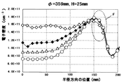
図19A〜図19Eに、突出部36Bの突出量Hおよび内径(直径)Φをパラメータとする電子密度空間分布特性の一例(実験データ)を示す。この実験でもプラズマ吸収プローブ(PAP)を用いて半径方向の各位置における電子密度を測定した。ただし、半導体ウエハの口径を300mmとしている。主たるパラメータΦ,Hは、図19Aの実験例ではΦ=329mm、H=15mm、図19Bの実験例ではΦ=329mm、H=20mm、図19Cの実験例ではΦ=339mm、H=20mm、図19Dの実験例ではΦ=349mm、H=20mm、図19Eの実験例ではΦ=359mm、H=25mmである。また、副次的なパラメータとして、内側投入電力Piと外側投入電力Poの比率Pi/Po(RFパワー比)を(30/70)、(27/73)、(20/80)、(14/86)の4通りに選んでいる。
19A to 19E show an example (experimental data) of electron density spatial distribution characteristics using the protrusion amount H and the inner diameter (diameter) Φ of the
図19A〜図19Eの実験データから、電子密度の急激にドロップする変曲点Fが、外側上部電極36における突出部36Bの内径(直径)Φを大きくするほど半径方向外側へ移動し、突出部36Bの突出量Hを大きくするほど上がることがわかる。理想的な特性は、変曲点Fがウエハエッジ位置(150mm位置)の真上に位置し、かつ中心部側とのフラットな関係を高い位置で維持している分布特性である。その点では、図19Dの特性(Φ=349mm、H=20mm)、特にRFパワー比Pi/Poを30/70に選んだ場合の特性が最も理想値に近いといえる。
From the experimental data of FIGS. 19A to 19E, the inflection point F at which the electron density drops suddenly moves outward in the radial direction as the inner diameter (diameter) Φ of the
図20Aに、Φ,Hを二次元パラメータとする電子密度空間分布のトータル均一性UTおよびエッジ均一性UEの特性を示す。ここで、トータル均一性UTとは、図20Bに示すように、ウエハ中心位置(R0)からウエハエッジ位置(R150)までの半径方向全区間の面内均一性である。また、エッジ均一性UEは、ウエハエッジ付近の領域たとえば半径130mmの位置(R130)からウエハエッジ位置(R150)までの区間における面内均一性である。 FIG. 20A shows the characteristics of the total uniformity U T and the edge uniformity U E of the electron density spatial distribution with Φ and H as two-dimensional parameters. Here, as shown in FIG. 20B, the total uniformity U T is the in-plane uniformity of the entire radial section from the wafer center position (R 0 ) to the wafer edge position (R 150 ). The edge uniformity U E is an in-plane uniformity in a region near the wafer edge, for example, a section from a position (R 130 ) having a radius of 130 mm to a wafer edge position (R 150 ).
図20Aの特性から、突出部36Bの突出量Hはトータル均一性UTを大きく左右し、エッジ均一性UEに対しても大きな影響力を有することがわかる。一方、突出部36Bの内径(直径)Φは、エッジ均一性Eに対して作用するものの、トータル均一性Tには殆ど影響しないことがわかる。総じて、突出部36Bの突出量Hは、25mm以下とするのが好ましく、特に20mm付近に選ぶのが最も好ましいといえる。また、突出部36Bの内径(直径)Φは、348mm〜360mmの範囲内に選ぶのが好ましく、特に349mm付近に選ぶのが最も好ましいといえる。なお、Φ=348mm〜360mmは、突出部36Bがウエハのエッジよりも半径方向外側に24mm〜30mm離れた位置に配置されることを意味する。重要なことは、外側上部電極36の突出部36Bは、プラズマ生成空間に対して周辺側から半径方向内向きの電界を与えることによりプラズマを閉じ込める作用を奏する点であり、このことからプラズマ密度空間分布特性の均一性を図るにはウエハのエッジよりも半径方向外側に位置することが必須といえるほど望ましい。一方で、突出部36Bの径方向の幅サイズは重要ではなく、任意の幅サイズに選んでよい。
From the characteristics of FIG. 20A, it can be seen that the protrusion amount H of the
図21に、第3の実施例における特徴部分の構成を示す。特徴以外の部分は、上記第2の実施例のものと同じでよい。この第3の実施例の特徴は、上記第2の実施例における外側上部電極36の突出部36B回りにシールド部材104を設ける構成である。
FIG. 21 shows the structure of the characteristic part in the third embodiment. Portions other than the features may be the same as those in the second embodiment. The feature of the third embodiment is that the
このシールド部材104は、たとえば表面をアルマイト処理されたアルミニウム板からなり、処理容器10の側壁に物理的かつ電気的に結合され、容器側壁から外側上部電極36の突出部36Bの下までほぼ水平に延びており、突出部36Bおよびリング形遮蔽部材42の下面を非接触または絶縁状態で覆っている。外側上部電極36の下部電極部材36Bは断面L形に構成され、外周側の部分が垂直下方に延びて突出部を形成している。この突出部の突出量Hおよび内径Φは上記第2実施例と同様の数値条件で選ばれてよい。
The
シールド部材104の機能は、外側上部電極36の突出部36Bの下面およびリング形遮蔽部材42の下面からの高周波放電を遮断また封印して、その直下におけるプラズマ生成を抑制することである。これにより、一次的にはプラズマをウエハ直上に閉じ込める効果を一層高めることができる。
The function of the
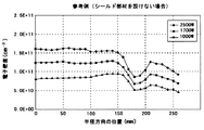
図22Aおよび図22Bに、シールド部材104によるプラズマ閉じ込め効果の実証例(実験データ)を示す。シールド部材104を設けない場合は、図22Bに示すように、半径方向においてプラズマ電子密度がウエハエッジ位置(150mm)の外側でいったんドロップしてから再び上昇して山を形成している。これは、外側上部電極36の突出部36Bの下面およびリング形遮蔽部材42の下面から垂直下方に高周波電力が放出されることにより、その直下でもプラズマが生成され、電子やイオンが存在しているためである。このように、ウエハエッジ位置より径方向外側に相当離れた空間内に相当量のプラズマが存在することにより、そのぶんウエハ直上のプラズマ密度が薄められている。
22A and 22B show a demonstration example (experimental data) of the plasma confinement effect by the
これに対して、この実施例のようにシールド部材104を設けた場合は、図22Aに示すように、電子密度(プラズマ密度)はウエハエッジ位置(150mm)の外側では半径方向外側に向って実質的に単調減少し、逆にウエハ直上では全体的に増大している。これは、シールド部材104の存在により、外側上部電極36の突出部36Bの下面およびリング形遮蔽部材42の下面が高周波の通り路ではなくなり、その直下でのプラズマ生成が大幅に減少するためである。また、高周波電源52のRFパワーを大きくするほど、シールド部材104によるプラズマ閉じ込め効果なしプラズマ拡散防止効果も大きくなることがわかる。
On the other hand, when the
さらに、二次的効果として、上記のようにシールド部材104によりウエハエッジ位置の外側でプラズマ生成を大幅に弱められることにより、その付近でのラジカルやイオン等のエッチング種も少なくし、不所望な重合膜が容器内の各部(特にシールド部材104付近)に付着するのを効果的に防止することができる。たとえば、従来より、Low-k膜(低誘電率層間絶縁膜)のエッチング加工では、プラズマエッチングの後に同一チャンバ内でO2ガスを用いてアッシング(レジスト除去)を行う際、先のプラズマエッチングで容器内にポリマーの形態で付着していた反応種(たとえばCF,F等)がプラズマ中の活性な酸素原子により誘起されてLow-k膜のビアホールをボーイング形状に削ったり膜内に侵入してk値を変える等のダメージ(Low-kダメージ)を生ずることがあった。しかし、この実施例によれば、プラズマエッチングにおける反応種の不所望な堆積をシールド部材104で効果的に抑止できるため、上記のようなLow-kダメージの問題も解決することができる。なお、シールド部材104は、任意の導電材または半導体(たとえばシリコン)を材質とすることが可能であり、異なる材質を組み合わせて構成してもよい。
Further, as a secondary effect, as described above, the
図21では、上部電極34(36,38)に冷媒通路106,108を設ける構成も示している。これらの冷媒通路106,108にはそれぞれ配管110,112を介してチラー装置(図示せず)より温調された冷却媒体が循環供給される。外側上部電極36においては、上部電極部材36Aに冷媒通路106が設けられる。下部電極部材36Bは、熱コンダクタンスを高めるコーティングまたはシート102によって上部電極部材36Aに結合されているため、冷却機構による冷却を効果的に受けることができる。
FIG. 21 also shows a configuration in which the
なお、高周波電源52,90をオフにしている間も、各電極には冷媒が供給される。従来より、この種のプラズマ処理装置において、たとえばガルデン等の絶縁性の冷媒を使用する場合は、冷媒が冷媒通路を流れる際に摩擦で発生する静電気によって電極が異常な高電圧状態となり、高周波電源オフ中のメンテナンス等で人の手が触れると感電するおそれがあった。しかし、本発明のプラズマ処理装置においては、ローパスフィルタ92(図8)内の抵抗器93を通して内側上部電極38に発生した静電気をグランドに逃がすことが可能であり、感電の危険性を防止できる。
In addition, while the high
上記第3の実施例におけるプラズマエッチング装置(図8、図21)を使用し、シリコン酸化膜(SiO2)に開口径(Φ)0.22μmの孔を形成するエッチングにおいて、外側上部電極36および内側上部電極38に対するRF電力の投入比率(Pi/Po)をパラメータにしてエッチング特性(特にエッチングレート)を実験で評価した。他のエッチング条件は下記のとおりであり、図23〜図25に実験結果のデータを示す。
ウエハ口径=300mm
チャンバ内の圧力=20mTorr
温度(上部電極/チャンバ側壁/下部電極)=20/60/60゜C
伝熱ガス(Heガス)供給圧力(センター部/エッジ部)=20/35Torr
上部及び下部電極間距離=45mm
外側上部電極の突出量(H)=15mm
プロセスガス(C5F8/CH2F2/N2/Ar/O2)≒10/20/110/560/10sccm
高周波電力(60MHz/2MHz)≒2300W/3500W
エッチング時間=120秒
In the etching for forming a hole having an opening diameter (Φ) of 0.22 μm in the silicon oxide film (SiO 2 ) using the plasma etching apparatus (FIGS. 8 and 21) in the third embodiment, the outer
Wafer diameter = 300mm
Pressure in chamber = 20 mTorr
Temperature (upper electrode / chamber sidewall / lower electrode) = 20/60/60 ° C
Heat transfer gas (He gas) supply pressure (center / edge) = 20/35 Torr
Distance between upper and lower electrodes = 45mm
Projection amount of outer upper electrode (H) = 15 mm
Process gas (C 5 F 8 / CH 2 F 2 / N 2 / Ar / O 2 ) ≈10 / 20/110/560/10 sccm
High frequency power (60MHz / 2MHz) ≒ 2300W / 3500W
Etching time = 120 seconds
図23に示すように、内側投入電力Piの比率を14%、18%、30%と上げていくと、電子密度つまりプラズマ密度は、ウエハ中心部付近ではPiの比率に比例して高くなる一方で、ウエハエッジ部付近ではそれほど変わらない。このことから、RF電力の投入比率(Pi/Po)を可変することで、径方向におけるプラズマ密度の空間分布特性を制御できることがわかる。 As shown in FIG. 23, when the ratio of the inner input power P i is increased to 14%, 18%, and 30%, the electron density, that is, the plasma density increases in proportion to the ratio of P i near the center of the wafer. On the other hand, it does not change so much near the wafer edge. From this, it can be seen that the spatial distribution characteristics of the plasma density in the radial direction can be controlled by varying the RF power input ratio (P i / P o ).
図24は、RF電力の投入比率(Pi/Po)を可変したときにラジカル密度の受ける影響をみるために、ラジカル密度と比例関係にある反応生成物や反応種で形成される重合膜の堆積速度を半径方向の各位置で測定した結果を示す。なお、重合膜を堆積させるサンプル基板にベアシリコンウエハを用いた。図24の実験データから、RF電力の投入比率(Pi/Po)を可変しても、重合膜の堆積速度つまりラジカル密度の空間分布特性に与える影響は非常に少ないことが確認された。 FIG. 24 shows a polymer film formed of reaction products and reaction species proportional to the radical density in order to see the influence of the radical density when the RF power input ratio (P i / P o ) is varied. The result of having measured the deposition speed of each in each position of radial direction is shown. A bare silicon wafer was used as a sample substrate on which the polymer film was deposited. From the experimental data of FIG. 24, it was confirmed that even if the input ratio (P i / P o ) of RF power was varied, the influence on the deposition rate of the polymer film, that is, the spatial distribution characteristics of the radical density was very small.
図25は、上記SiO2のエッチングにおいてウエハ上の半径方向の各位置で測定したエッチング深さを示す。図示のように、内側投入電力Piの比率を14%、18%、30%と上げていくと、エッチング深さは、ウエハ中心部付近ではPiの比率に比例して大きくなる一方で、ウエハエッジ部付近ではそれほど変わらない。つまり、電子密度(図24)と同様の傾向を示す。
FIG. 25 shows the etching depth measured at each position in the radial direction on the wafer in the SiO 2 etching. As shown, 14% of the ratio of the inner
このように、図23〜図25の実験データから、本発明においては、外側上部電極36および内側上部電極38に対するRF電力の投入比率(Pi/Po)を可変することで、ラジカル密度の空間分布特性に実質的な影響を及ぼすことなく、つまりラジカル密度の空間分布制御から独立して、径方向におけるプラズマ密度の空間分布を制御し、それによってエッチング深さつまりエッチングレートの均一性を改善できることが確認された。なお、上記第1または第2の実施例におけるプラズマエッチング装置(図1、図8、図18)を使用しても、上記と同様の実験結果が得られることは明らかである。
As described above, from the experimental data of FIGS. 23 to 25, in the present invention, by changing the input ratio (P i / P o ) of the RF power with respect to the outer
上記第3の実施例のプラズマエッチング装置(図8、図21)でCF系の処理ガスを使用するシリコン酸化膜(SiO2)のエッチングにおいて、中心シャワーヘッド(62,56a)より噴射される処理ガスの流量FCと周辺シャワーヘッド(64,56a)より噴射される処理ガスの流量FEとの比率(FC/FE)をパラメータにして、各ラジカルまたは各反応生成物の分布をシミュレーションで評価した。このシミュレーションでは、ウエハ表面では反応が起こらず反応生成物や反応種の吸着も生じないものとし、ブランケットSiO2膜上で単純に下記の反応が起きているものと仮定した。
2CF2+SiO2→SiF4+2CO
In the etching of the silicon oxide film (SiO 2 ) using a CF-based processing gas in the plasma etching apparatus of the third embodiment (FIGS. 8 and 21), the processing sprayed from the central shower head (62, 56a) Using the ratio (F C / F E ) between the flow rate F C of the gas and the flow rate F E of the processing gas injected from the peripheral shower head (64, 56a) as a parameter, the distribution of each radical or each reaction product is simulated. It was evaluated with. In this simulation, it was assumed that no reaction occurred on the wafer surface and no adsorption of reaction products or reactive species occurred, and that the following reaction was simply performed on the blanket SiO 2 film.
2CF 2 + SiO 2 → SiF 4 + 2CO
他の主なエッチング条件は下記のとおりであり、図26〜図30に各ラジカルまたは各反応生成物についてのシミュレーション結果を示す。図31には、主エッチングガス(C4F8)の分子から段階的な解離によって生成されるラジカルの種類と発生率(括弧内%数字)を示している。
ウエハ口径=200mm
チャンバ内の圧力=50mTorr
温度(上部電極/チャンバ側壁/下部電極)=20/60/60゜C
伝熱ガス(Heガス)供給圧力(センター部/エッジ部)=10/35Torr
上部及び下部電極間距離=30mm
外側上部電極の突出量(H)=15mm
プロセスガス(C4F8/N2/Ar)≒5/120/1000sccm
高周波電力(60MHz/2MHz)≒1200W/1700W
Other main etching conditions are as follows, and FIGS. 26 to 30 show simulation results for each radical or each reaction product. Figure 31 shows the main etching gas (C 4 F 8) type and incidence of radicals generated by the gradual dissociation from molecules (in parentheses% number).
Wafer diameter = 200 mm
Pressure in chamber = 50 mTorr
Temperature (upper electrode / chamber sidewall / lower electrode) = 20/60/60 ° C
Heat transfer gas (He gas) supply pressure (center / edge) = 10/35 Torr
Distance between upper and lower electrodes = 30 mm
Projection amount of outer upper electrode (H) = 15 mm
Process gas (C 4 F 8 / N 2 / Ar) ≈5 / 120/1000 sccm
High frequency power (60MHz / 2MHz) ≒ 1200W / 1700W
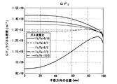
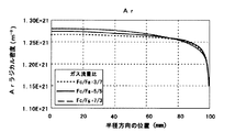
図26に示すように、主たる反応種であるCF2の密度分布特性は、中心/周辺ガス流量比率(FC/FE)に大きく左右される。すなわち、中心ガス流量FCの比率を上げるほどウエハ中心部付近のCF2密度は高くなる一方で、ウエハエッジ部付近のCF2密度は殆ど変わらない。図28に示すように、COラジカルの密度分布特性も中心/周辺ガス流量比率(FC/FE)に対して同様の変化を示す。もっとも、図27に示すように、Arラジカルの密度分布特性は中心/周辺ガス流量比率(FC/FE)に対して殆ど変化しない。 As shown in FIG. 26, the density distribution characteristic of CF 2 which is the main reactive species greatly depends on the center / peripheral gas flow rate ratio (F C / F E ). That is, as the ratio of the central gas flow rate F C is increased, the CF 2 density near the wafer center increases, while the CF 2 density near the wafer edge hardly changes. As shown in FIG. 28, the density distribution characteristics of CO radicals show the same change with respect to the center / peripheral gas flow rate ratio (F C / F E ). However, as shown in FIG. 27, the density distribution characteristics of Ar radicals hardly change with respect to the center / peripheral gas flow rate ratio (F C / F E ).
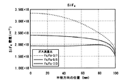
反応生成物についてみると、図29および図30に示すように、SiF4密度およびCO密度のいずれも中心/周辺ガス流量比率(FC/FE)に大きく左右される。より詳細には、中心ガス流量FCの比率を下げるほどウエハ中心部付近のSiF4,COの密度は高くなる一方で、ウエハエッジ部付近では殆ど変わらない。中心ガス流量FCと周辺ガス流量FEを同じ(FC/FE=50/50)にしても、ウエハ中心部付近の方がウエハエッジ部付近よりも高くなる。このように中心部側に反応生成物が溜まりやすいのは、上方からの新鮮なガス流で反応生成物が側方へ押しのけられる作用が周辺部よりも弱いためである。ウエハ上で反応生成物が不均一に分布すると、各位置の処理ガス供給率や化学反応の均一性に影響するだけでなく、エッチング形状や選択性等が直接影響を受けることもある。この実施例では、図29および図30からわかるように、中心ガス流量FCを周辺ガス流量FEよりも多めに(図示の例ではFC/FE=70/30近辺に)設定することで、反応生成物の空間密度分布を均一化することができた。なお、上記第1または第2の実施例におけるプラズマエッチング装置(図1、図8、図18)を使用しても、上記と同様のシミュレーション結果が得られる。 As for the reaction product, as shown in FIGS. 29 and 30, both the SiF 4 density and the CO density are greatly influenced by the center / peripheral gas flow rate ratio (F C / F E ). More specifically, while the more the density of the SiF 4, CO near the wafer center portion is higher lowering the ratio of the core gas flow F C, hardly changes in the vicinity of the wafer edge portion. Even if the central gas flow rate F C and the peripheral gas flow rate F E are the same (F C / F E = 50/50), the vicinity of the wafer center is higher than the vicinity of the wafer edge. The reason why the reaction product tends to accumulate on the center side in this manner is that the action of pushing the reaction product to the side by a fresh gas flow from above is weaker than that of the peripheral portion. If the reaction product is unevenly distributed on the wafer, not only the processing gas supply rate at each position and the uniformity of the chemical reaction are affected, but also the etching shape and selectivity may be directly affected. In this embodiment, as can be seen from FIGS. 29 and 30, the center gas flow rate F C is set to be larger than the peripheral gas flow rate F E (in the illustrated example, around F C / F E = 70/30). Thus, the spatial density distribution of the reaction product could be made uniform. Even if the plasma etching apparatus (FIG. 1, FIG. 8, FIG. 18) in the first or second embodiment is used, the same simulation results as described above can be obtained.
上記第3の実施例のプラズマエッチング装置(図8、図21)を使用し、BARC(反射防止膜)のエッチングにおいて中心/周辺ガス流量比率(FC/FE)をパラメータにしてエッチング形状と選択性を評価した。図32Aに評価サンプルを示す。マスク開口径(Φ)0.12μm、フォトレジストの膜厚350nm、BARCの膜厚80nm、SiO2の膜厚700nmであり、選択性の評価項目として「オキサイドロス」と「レジスト残量」を測定し、エッチング形状または寸法精度の評価項目として「ボトムCD」を測定した。図32BにFC/FE=50/50に設定したときの各評価項目の測定値を示し、図32CにFC/FE=70/30に設定したときの各評価項目の測定値を示す。測定ポイントの「センター」はウエハの中心点の位置であり、「エッジ」はウエハのノッチ端から中心点に向って5mmの位置である。主なエッチング条件は下記のとおりである。
ウエハ口径=300mm
チャンバ内の圧力=150mTorr
伝熱ガス(Heガス)供給圧力(センター部/エッジ部)=10/25Torr
上部及び下部電極間距離=30mm
外側上部電極の突出量(H)=15mm
プロセスガス(CF4)≒200sccm
高周波電力(60MHz/2MHz)≒500W/600W
エッチング時間=30秒
Using the plasma etching apparatus (FIGS. 8 and 21) of the third embodiment, the etching shape and the center / peripheral gas flow rate ratio (F C / F E ) are used as parameters in the etching of the BARC (antireflection film). Selectivity was evaluated. FIG. 32A shows an evaluation sample. It has a mask opening diameter (Φ) of 0.12 μm, a photoresist film thickness of 350 nm, a BARC film thickness of 80 nm, and a SiO 2 film thickness of 700 nm, and measures “oxide loss” and “resist remaining amount” as evaluation items for selectivity. Then, “bottom CD” was measured as an evaluation item of etching shape or dimensional accuracy. FIG. 32B shows the measured values of each evaluation item when F C / F E = 50/50, and FIG. 32C shows the measured values of each evaluation item when F C / F E = 70/30. Show. The “center” of the measurement point is the position of the center point of the wafer, and the “edge” is a position of 5 mm from the notch end of the wafer toward the center point. The main etching conditions are as follows.
Wafer diameter = 300mm
Pressure in chamber = 150 mTorr
Heat transfer gas (He gas) supply pressure (center / edge) = 10/25 Torr
Distance between upper and lower electrodes = 30 mm
Projection amount of outer upper electrode (H) = 15 mm
Process gas (CF 4 ) ≈ 200 sccm
High frequency power (60MHz / 2MHz) ≒ 500W / 600W
Etching time = 30 seconds
このBARCエッチングの評価項目において、「オキサイドロス」はBARCエッチングの延長として下地膜のSiO2を削った深さであり、この値は小さいほど好ましいが、それ以上にウエハ上のばらつき(特にセンターとエッジ間のばらつき)が小さいほど好ましい。「レジスト残量」はエッチングの終了後に残っているフォトレジストの厚さであり、この値は大きいほど好ましく、やはりばらつきが小さいほど好ましい。「ボトムCD」はBARCに形成された孔の底の直径であり、この値はマスク径Φに近いほど好ましいが、やはりばらつきが小さいほど好ましい。 In this evaluation item of BARC etching, “Oxide loss” is the depth of SiO 2 removal of the underlying film as an extension of BARC etching, and this value is preferably as small as possible. The smaller the variation between edges, the better. The “resist remaining amount” is the thickness of the photoresist remaining after the etching is completed, and this value is preferably as large as possible, and also as the variation is small. “Bottom CD” is the diameter of the bottom of the hole formed in the BARC, and this value is preferably as close as possible to the mask diameter Φ, but is also preferable as the variation is small.
図32Bに示すように、中心ガス流量FCと周辺ガス流量FEとを同量(5:5)に設定したときは、全ての評価項目において、センターとエッジ間のばらつきが大きく、特に「レジスト残量」のばらつきが大きい。これに対して、中心ガス流量FCを周辺ガス流量FEよりも多め(7:3)に設定した場合は、図32Cに示すように、全ての評価項目が良好な値で均一に安定し、選択性およびエッチング形状が著しく改善されている。 As shown in FIG. 32B, when the central gas flow rate F C and the peripheral gas flow rate F E are set to the same amount (5: 5), the variation between the center and the edge is large in all evaluation items. The variation of “resist remaining amount” is large. On the other hand, when the central gas flow rate F C is set to be larger (7: 3) than the peripheral gas flow rate F E , all the evaluation items are uniformly stabilized at good values as shown in FIG. 32C. The selectivity and etching shape are significantly improved.
このように、処理容器10内で、特に上部電極34と下部電極16との間に設定されたプラズマ生成空間において、上部電極34の内側上部電極38に設けられた中心シャワーヘッド(62,56a)より噴射される処理ガスの流量FCと周辺シャワーヘッド(64,56a)より噴射される処理ガスの流量FEとの比率(FC/FE)を調整することで、ラジカル密度の空間分布を制御し、ラジカルベースによるエッチング特性(選択性、エッチング形状等)の均一化を達成することができる。なお、上記第1または第2の実施例におけるプラズマエッチング装置(図1、図8、図18)を使用しても、上記と同様の測定結果が得られる。
Thus , in the
上記第3の実施例のプラズマエッチング装置(図8、図21)を使用し、SiO2膜のエッチングにおいて中心/周辺ガス流量比率(FC/FE)をパラメータにしてエッチング形状を評価した。図33Aに評価サンプルを示す。マスク開口径(Φ)0.22μm、フォトレジストの膜厚500nm、BARCの膜厚100nm、SiO2の膜厚1μmであり、エッチング形状の評価項目として「エッチング深さ」、「トップCD」、「ボトムCD」を測定した。図33BにFC/FE=50/50に設定したときの各評価項目の測定値を示し、図33CにFC/FE=10/90に設定したときの各評価項目の測定値を示す。主なエッチング条件は下記のとおりである。
ウエハ口径=300mm
チャンバ内の圧力=20mTorr
温度(上部電極/チャンバ側壁/下部電極)=20/60/60゜C
伝熱ガス(Heガス)供給圧力(センター部/エッジ部)=20/35Torr
上部及び下部電極間距離=45mm
外側上部電極の突出量(H)=15mm
プロセスガス(C5F8/CH2F2/N2/Ar/O2)≒10/20/110/560/10sccm
高周波電力(60MHz/2MHz)≒2300W/3500W
RFパワー比(内側投入電力Pi/外側投入電力Po)=30:70
エッチング時間=120秒
Using the plasma etching apparatus (FIGS. 8 and 21) of the third embodiment, the etching shape was evaluated using the center / peripheral gas flow rate ratio (F C / F E ) as a parameter in the etching of the SiO 2 film. FIG. 33A shows an evaluation sample. The mask opening diameter (Φ) is 0.22 μm, the thickness of the photoresist is 500 nm, the thickness of the BARC is 100 nm, the thickness of the SiO 2 is 1 μm, and “etching depth”, “top CD”, “ "Bottom CD" was measured. Shows measurement values of the respective evaluation items when set to F C / F E = 50/ 50 in FIG. 33B, the measurement value of each evaluation item when set to F C / F E = 10/ 90 in FIG. 33C Show. The main etching conditions are as follows.
Wafer diameter = 300mm
Pressure in chamber = 20 mTorr
Temperature (upper electrode / chamber sidewall / lower electrode) = 20/60/60 ° C
Heat transfer gas (He gas) supply pressure (center / edge) = 20/35 Torr
Distance between upper and lower electrodes = 45mm
Projection amount of outer upper electrode (H) = 15 mm
Process gas (C 5 F 8 / CH 2 F 2 / N 2 / Ar / O 2 ) ≈10 / 20/110/560/10 sccm
High frequency power (60MHz / 2MHz) ≒ 2300W / 3500W
RF power ratio (inside input power P i / outside input power P o ) = 30: 70
Etching time = 120 seconds
このSiO2エッチングの評価項目において、「エッチング深さ」は、エッチング時間(120秒)の間にSiO2膜に形成された孔の深さであり、エッチング速度に相当する。「トップCD」および「ボトムCD」は、SiO2膜に形成された孔の上端および下端(底)の直径であり、両者の値が近いほど垂直形状性(異方性)にすぐれている。もちろん、いずれの評価項目も、「センター」と「エッジ」との間でばらつきが小さいほど好ましい。 In this SiO 2 etching evaluation item, “etching depth” is the depth of holes formed in the SiO 2 film during the etching time (120 seconds), and corresponds to the etching rate. “Top CD” and “bottom CD” are the diameters of the upper end and lower end (bottom) of the hole formed in the SiO 2 film, and the closer both values are, the better the vertical shape (anisotropy) is. Of course, it is preferable that any evaluation item has a smaller variation between the “center” and the “edge”.
図33Bに示すように、中心ガス流量FCと周辺ガス流量FEとを同量(5:5)に設定したときは、「エッチング深さ」のばらつきがあるだけでなく各位置でボトムCD/トップCD比が小さくテーパ化の傾向が大きい。これに対して、中心ガス流量FCを周辺ガス流量FEよりも少なめ(1:9)に設定した場合は、図33Cに示すように、「エッチング深さ」つまりエッチング速度が均一化されるとともに、垂直形状性の向上と均一化も図れた。 As shown in FIG. 33B, when the central gas flow rate F C and the peripheral gas flow rate F E are set to the same amount (5: 5), not only the “etching depth” varies but also the bottom CD at each position. / The top CD ratio is small and the tendency to taper is large. On the other hand, when the central gas flow rate F C is set to be smaller (1: 9) than the peripheral gas flow rate F E , as shown in FIG. 33C, the “etching depth”, that is, the etching rate is made uniform. At the same time, the vertical shape was improved and made uniform.
このように、この実施例でも、内側ガス流量FCと外側ガス流量FEの比率(FC/FE)を調整することで、ラジカル密度の空間分布を制御し、ラジカルベースによるエッチング特性(特にエッチング形状)の均一化を達成できることが確認された。なお、上記第1または第2の実施例におけるプラズマエッチング装置(図1、図8、図18)を使用しても、上記と同様の測定結果が得られる。 Thus, also in this embodiment, by adjusting the ratio (F C / F E ) between the inner gas flow rate F C and the outer gas flow rate F E , the spatial distribution of radical density is controlled, and radical-based etching characteristics ( In particular, it was confirmed that uniform etching shape) can be achieved. Even if the plasma etching apparatus (FIG. 1, FIG. 8, FIG. 18) in the first or second embodiment is used, the same measurement result as above can be obtained.
上記のように、処理容器10内に設定されたプラズマ生成空間においてプラズマ密度分布の制御とラジカル密度分布の制御とを独立に行える。このことにより、たとえば図34のマップに示すように多種多用なプラズマ処理のアプリケーションに2系統の独立制御で好適に対応することができる。
As described above, the plasma density distribution and the radical density distribution can be controlled independently in the plasma generation space set in the
以上に述べた実施の形態および実施例は、本発明の技術思想に基づいて種々の変形が可能である。 The embodiments and examples described above can be variously modified based on the technical idea of the present invention.
たとえば、第1の高周波電源52からの高周波を整合器44や給電筒50等を介して外側上部電極36だけに供給し、内側上部電極38には供給しない構成も可能である。その場合でも、内側上部電極38はシャワーヘッドとして機能したり、第2の高周波電源90からの高周波をグランドへ流すための電極として機能することができる。あるいは、内側上部電極38を電極機能を有しない専用のシャワーヘッドに置き換えることも可能である。また、上記した実施形態では外側上部電極36を1つまたは単体のリング状電極で構成したが、全体でリング状に配置される複数の電極で構成することも可能である。また、外側上部電極36の内径を非常に小さくする構成や、外側上部電極36を円盤形状に構成することも可能である。また、第2の高周波電源90を省くことができる。本発明は、プラズマエッチングに限らず、プラズマCVD、プラズマ酸化、プラズマ窒化、スパッタリングなど種々のプラズマ処理に適用可能である。また、本発明における被処理基板は半導体ウエハに限るものではなく、フラットパネルディスプレイ用の各種基板や、フォトマスク、CD基板、プリント基板等も可能である。
For example, a configuration in which the high frequency from the first high
10 チャンバ(処理容器)
16 サセプタ(下部電極)
34 上部電極
36 外側上部電極
36A 上部電極部材
36B 下部電極部材
38 内側上部電極
40 誘電体
44 整合器
48 コネクタ
50 給電筒
52 第1の高周波電源
56 電極板
58 電極支持板
60 環状隔壁部材
62 中心ガス導入室
(62,56a) 中心シャワーヘッド
64 周辺ガス導入室
(64,56a) 周辺シャワーヘッド
66 処理ガス供給源
68 ガス供給管
70a,70b 流量制御弁
84 排気装置
90 第2の高周波電源
92 ローパスフィルタ
93 可変抵抗器
94 ハイパスフィルタ
100 導体部材
102 シールド部材
10 chamber (processing vessel)
16 Susceptor (lower electrode)
34
Claims (26)
前記処理容器内で所定位置に配置される被処理基板と対向するように設置される上部電極と、
前記処理容器内に処理ガスを供給する処理ガス供給部と、
第1の高周波を出力する第1の高周波電源と、
前記上部電極に周回方向で連続的に接続される第1の筒状導電部材を有し、前記第1の高周波電源からの前記第1の高周波を前記上部電極に印加する給電部と、
前記上部電極の下面の一部を覆うシールド部材と
を有し、
前記シールド部材が、前記上部電極から電気的に分離し、グランドに接地されている前記処理容器に電気的に接続される、
プラズマ処理装置。 A processing container capable of being vacuumed;
An upper electrode installed so as to face a substrate to be processed disposed at a predetermined position in the processing container;
A processing gas supply unit for supplying a processing gas into the processing container;
A first high frequency power source for outputting a first high frequency;
A power supply unit that has a first cylindrical conductive member continuously connected to the upper electrode in a circumferential direction, and that applies the first high frequency from the first high frequency power source to the upper electrode;
A shield member covering a part of the lower surface of the upper electrode,
The shield member is electrically separated from the upper electrode and electrically connected to the processing vessel grounded to ground;
Plasma processing equipment.
前記処理容器内で所定位置に配置される被処理基板と対向するように設置される上部電極と、
前記処理容器内に処理ガスを供給する処理ガス供給部と、
第1の高周波を出力する第1の高周波電源と、
前記上部電極に周回方向で連続的に接続される第1の筒状導電部材を有し、前記第1の高周波電源からの前記第1の高周波を前記上部電極に印加する給電部と
を有し、
前記上部電極を、前記給電部に接続される第1の電極部材と、前記基板と対向するように前記第1の電極部材の下面に着脱可能に密着して固定される第2の電極部材とで構成し、
前記第1の電極部材に冷媒を通すための冷媒通路を設け、
前記第1の電極部材と前記第2の電極部材との間に熱抵抗を低くするための膜またはシートを設ける、
プラズマ処理装置。 A processing container capable of being vacuumed;
An upper electrode installed so as to face a substrate to be processed disposed at a predetermined position in the processing container;
A processing gas supply unit for supplying a processing gas into the processing container;
A first high frequency power source for outputting a first high frequency;
A first cylindrical conductive member that is continuously connected to the upper electrode in a circumferential direction, and a power feeding unit that applies the first high frequency from the first high frequency power source to the upper electrode. ,
A first electrode member connected to the power feeding portion; a second electrode member fixed in close contact with the lower surface of the first electrode member so as to face the substrate; Consisting of
Providing a coolant passage for passing the coolant through the first electrode member;
A film or sheet for reducing thermal resistance is provided between the first electrode member and the second electrode member.
Plasma processing equipment.
前記第1の筒状導電部材は、前記外側上部電極に接続される、
請求項1〜8、11〜16のいずれか一項に記載のプラズマ処理装置。 The upper electrode includes an inner upper electrode and a ring-shaped outer upper electrode disposed in a state of being electrically insulated from the inner upper electrode in a radial direction outside the inner upper electrode,
The first cylindrical conductive member is connected to the outer upper electrode.
The plasma processing apparatus as described in any one of Claims 1-8 and 11-16.
前記第1の高周波電源からの前記第1の高周波は、前記内側上部電極と前記外側上部電極の両方に供給される、
請求項17に記載のプラズマ処理装置。 The power feeding unit further includes a central conductive member connected to the center of the inner upper electrode,
The first high frequency from the first high frequency power supply is supplied to both the inner upper electrode and the outer upper electrode.
The plasma processing apparatus according to claim 17.
前記第1の高周波電源からの前記第1の高周波は、前記導電コネクタによって前記中心導電部材と前記第1の筒状導電部材とに分岐して供給される、
請求項18に記載のプラズマ処理装置。 The power feeding unit has a conductive connector that connects the central conductive member and the first cylindrical conductive member,
The first high frequency from the first high frequency power supply is branched and supplied to the central conductive member and the first cylindrical conductive member by the conductive connector.
The plasma processing apparatus according to claim 18.
前記処理容器内で所定位置に配置される被処理基板と対向するようにリング状に設置される1つまたは複数の外側上部電極と、
前記外側上部電極と前記処理容器の側壁との間に取り付けられるリング形状の絶縁性遮蔽部材と、
前記外側上部電極の半径方向内側に絶縁して配置される内側上部電極と、
前記処理容器内で前記基板を載置するために前記外側上部電極および前記内側上部電極と対向して設置される下部電極と、
前記処理容器内に処理ガスを供給する処理ガス供給部と、
第1の高周波を出力する第1の高周波電源と、
前記外側上部電極に周回方向で連続的に接続される第1の筒状導電部材を有し、前記第1の高周波電源からの前記第1の高周波を前記第1の筒状導電部材を介して前記外側上部電極に印加する第1の給電部と、
前記内側上部電極の中心に接続される棒状の中心導電部材を有し、前記第1の高周波電源からの前記第1の高周波を前記第1の給電部から分岐し前記中心導電部材を介して前記内側上部電極に供給する第2の給電部と、
前記第1の筒状導電部材の径方向外側に設けられる電気的にグランド電位に接続された第2の筒状導電部材と、
を有し、
前記第1の給電部の前記第1の筒状導電部材および前記外側上部電極と前記第2の筒状導電部材との間で前記第1の筒状導電部材および前記外側上部電極を外側導波路とする第1の同軸線路が形成され、
前記第2の給電部の前記中心導電部材と前記第2の筒状導電部材との間で前記中心導電部材を内側導波路とする第2の同軸線路が形成され、
前記処理容器内で生成される前記処理ガスのプラズマに対して、前記第1の高周波電源からの前記第1の高周波を前記第1の給電部と前記第2の給電部とに分配して、前記外側上部電極と前記内側上部電極とから並列的に供給する、
プラズマ処理装置。 A processing container capable of being vacuumed;
One or a plurality of outer upper electrodes installed in a ring shape so as to face a target substrate disposed at a predetermined position in the processing container;
A ring-shaped insulating shielding member attached between the outer upper electrode and the side wall of the processing vessel;
An inner upper electrode that is insulated and arranged radially inward of the outer upper electrode;
A lower electrode disposed opposite to the outer upper electrode and the inner upper electrode in order to place the substrate in the processing container;
A processing gas supply unit for supplying a processing gas into the processing container;
A first high frequency power source for outputting a first high frequency;
A first cylindrical conductive member continuously connected in a circumferential direction to the outer upper electrode; and the first high-frequency power from the first high-frequency power source is transmitted through the first cylindrical conductive member. A first power feeding unit applied to the outer upper electrode;
A rod-like central conductive member connected to the center of the inner upper electrode; and the first high frequency power from the first high frequency power source is branched from the first power feeding portion, and the central conductive member is interposed therebetween. A second power supply for supplying the inner upper electrode;
A second cylindrical conductive member electrically connected to the ground potential provided on the radially outer side of the first cylindrical conductive member;
Have
The first cylindrical conductive member and the outer upper electrode are disposed between the first cylindrical conductive member and the outer upper electrode and the second cylindrical conductive member of the first power feeding unit as an outer waveguide. A first coaxial line is formed,
A second coaxial line having the central conductive member as an inner waveguide is formed between the central conductive member and the second cylindrical conductive member of the second power feeding unit,
Distributing the first high frequency from the first high frequency power supply to the first power supply unit and the second power supply unit with respect to the plasma of the processing gas generated in the processing container, Supply in parallel from the outer upper electrode and the inner upper electrode,
Plasma processing equipment.
前記可変コンデンサのキャパシタンスを可変することにより、前記内側導波路のインピーダンスを可変して、前記外側上部電極から前記プラズマに供給される電力と、前記内側上部電極から前記プラズマに供給される電力との比率を調整する、
請求項23に記載のプラズマ処理装置。 The second power supply section has a variable capacitor;
By varying the capacitance of the variable capacitor, the impedance of the inner waveguide is varied, and the power supplied from the outer upper electrode to the plasma and the power supplied from the inner upper electrode to the plasma Adjust the ratio,
The plasma processing apparatus according to claim 23.
前記処理容器内で前記上部電極の直下に前記基板を配置する工程と、
前記処理ガス供給部より前記処理容器内に所望の処理ガスを供給する工程と、
前記処理容器内を所定の圧力で減圧状態に維持する工程と、
前記第1の高周波電源より前記第1の高周波を前記上部電極に印加して、高周波放電により前記処理ガスのプラズマを生成する工程と、
生成された前記プラズマを前記処理容器内で拡散させる工程と、
前記プラズマの下で前記基板に前記所望のプラズマ処理を施す工程と
を有するプラズマ処理方法。 A plasma processing method for performing desired plasma processing on a substrate to be processed using the plasma processing apparatus according to any one of claims 1 to 25,
Placing the substrate directly below the upper electrode in the processing vessel;
Supplying a desired processing gas into the processing container from the processing gas supply unit;
Maintaining the inside of the processing vessel in a reduced pressure state at a predetermined pressure;
Applying the first high frequency from the first high frequency power source to the upper electrode and generating plasma of the processing gas by high frequency discharge;
Diffusing the generated plasma in the processing vessel;
Applying the desired plasma treatment to the substrate under the plasma.
Priority Applications (7)
| Application Number | Priority Date | Filing Date | Title |
|---|---|---|---|
| JP2003358425A JP4584565B2 (en) | 2002-11-26 | 2003-10-17 | Plasma processing apparatus and plasma processing method |
| CNB2003801042923A CN100459059C (en) | 2002-11-26 | 2003-11-25 | Plasma processing method and apparatus |
| PCT/JP2003/015030 WO2004049420A1 (en) | 2002-11-26 | 2003-11-25 | Plasma processing apparatus and method |
| AU2003284684A AU2003284684A1 (en) | 2002-11-26 | 2003-11-25 | Plasma processing apparatus and method |
| KR1020057009448A KR100652983B1 (en) | 2002-11-26 | 2003-11-25 | Plasma processing apparatus and method |
| TW092133237A TW200416874A (en) | 2002-11-26 | 2003-11-26 | Plasma processing apparatus and method |
| US11/137,516 US7506610B2 (en) | 2002-11-26 | 2005-05-26 | Plasma processing apparatus and method |
Applications Claiming Priority (2)
| Application Number | Priority Date | Filing Date | Title |
|---|---|---|---|
| JP2002341949 | 2002-11-26 | ||
| JP2003358425A JP4584565B2 (en) | 2002-11-26 | 2003-10-17 | Plasma processing apparatus and plasma processing method |
Publications (2)
| Publication Number | Publication Date |
|---|---|
| JP2004193566A JP2004193566A (en) | 2004-07-08 |
| JP4584565B2 true JP4584565B2 (en) | 2010-11-24 |
Family
ID=32396265
Family Applications (1)
| Application Number | Title | Priority Date | Filing Date |
|---|---|---|---|
| JP2003358425A Expired - Lifetime JP4584565B2 (en) | 2002-11-26 | 2003-10-17 | Plasma processing apparatus and plasma processing method |
Country Status (7)
| Country | Link |
|---|---|
| US (1) | US7506610B2 (en) |
| JP (1) | JP4584565B2 (en) |
| KR (1) | KR100652983B1 (en) |
| CN (1) | CN100459059C (en) |
| AU (1) | AU2003284684A1 (en) |
| TW (1) | TW200416874A (en) |
| WO (1) | WO2004049420A1 (en) |
Families Citing this family (42)
| Publication number | Priority date | Publication date | Assignee | Title |
|---|---|---|---|---|
| US7951262B2 (en) | 2004-06-21 | 2011-05-31 | Tokyo Electron Limited | Plasma processing apparatus and method |
| KR101180125B1 (en) * | 2004-06-21 | 2012-09-05 | 도쿄엘렉트론가부시키가이샤 | Plasma processing device and method |
| US7988816B2 (en) | 2004-06-21 | 2011-08-02 | Tokyo Electron Limited | Plasma processing apparatus and method |
| JP4550507B2 (en) * | 2004-07-26 | 2010-09-22 | 株式会社日立ハイテクノロジーズ | Plasma processing equipment |
| US7507670B2 (en) * | 2004-12-23 | 2009-03-24 | Lam Research Corporation | Silicon electrode assembly surface decontamination by acidic solution |
| US7674393B2 (en) * | 2005-03-25 | 2010-03-09 | Tokyo Electron Limited | Etching method and apparatus |
| US7993489B2 (en) | 2005-03-31 | 2011-08-09 | Tokyo Electron Limited | Capacitive coupling plasma processing apparatus and method for using the same |
| JP4642528B2 (en) * | 2005-03-31 | 2011-03-02 | 東京エレクトロン株式会社 | Plasma processing apparatus and plasma processing method |
| JP2007234770A (en) * | 2006-02-28 | 2007-09-13 | Tokyo Electron Ltd | Plasma etching method, and computer-readable recording medium |
| US8157953B2 (en) | 2006-03-29 | 2012-04-17 | Tokyo Electron Limited | Plasma processing apparatus |
| JP5116983B2 (en) * | 2006-03-30 | 2013-01-09 | 東京エレクトロン株式会社 | Plasma processing method and plasma processing apparatus |
| US8034213B2 (en) | 2006-03-30 | 2011-10-11 | Tokyo Electron Limited | Plasma processing apparatus and plasma processing method |
| US7829463B2 (en) | 2006-03-30 | 2010-11-09 | Tokyo Electron Limited | Plasma processing method and plasma processing apparatus |
| JP5057768B2 (en) * | 2006-12-19 | 2012-10-24 | 株式会社ライフ技術研究所 | DC plasma deposition system |
| JP5474291B2 (en) * | 2007-11-05 | 2014-04-16 | 株式会社アルバック | Ashing equipment |
| JP2009239012A (en) * | 2008-03-27 | 2009-10-15 | Tokyo Electron Ltd | Plasma processing device and method of plasma etching |
| US8367965B2 (en) * | 2008-08-28 | 2013-02-05 | Hermes-Epitek Corp. | Electrode design for plasma processing chamber |
| US8992723B2 (en) * | 2009-02-13 | 2015-03-31 | Applied Material, Inc. | RF bus and RF return bus for plasma chamber electrode |
| US8703586B2 (en) * | 2009-09-25 | 2014-04-22 | Kyocera Corporation | Apparatus for forming deposited film and method for forming deposited film |
| JP5312369B2 (en) * | 2010-02-22 | 2013-10-09 | 東京エレクトロン株式会社 | Plasma processing apparatus and plasma processing method |
| TWI474365B (en) * | 2010-08-25 | 2015-02-21 | Canon Anelva Corp | And a method of manufacturing the plasma processing apparatus and apparatus |
| JP5709505B2 (en) * | 2010-12-15 | 2015-04-30 | 東京エレクトロン株式会社 | Plasma processing apparatus, plasma processing method, and storage medium |
| KR101171988B1 (en) | 2011-03-30 | 2012-08-07 | 엘아이지에이디피 주식회사 | Apparatus for plasma processing |
| TWI594667B (en) * | 2011-10-05 | 2017-08-01 | 應用材料股份有限公司 | Symmetric plasma process chamber |
| CN103377868A (en) * | 2012-04-14 | 2013-10-30 | 靖江先锋半导体科技有限公司 | Lower electrode apparatus in etching electrode machine |
| US10170279B2 (en) | 2012-07-20 | 2019-01-01 | Applied Materials, Inc. | Multiple coil inductively coupled plasma source with offset frequencies and double-walled shielding |
| US10249470B2 (en) * | 2012-07-20 | 2019-04-02 | Applied Materials, Inc. | Symmetrical inductively coupled plasma source with coaxial RF feed and coaxial shielding |
| US9082590B2 (en) | 2012-07-20 | 2015-07-14 | Applied Materials, Inc. | Symmetrical inductively coupled plasma source with side RF feeds and RF distribution plates |
| US9449794B2 (en) * | 2012-07-20 | 2016-09-20 | Applied Materials, Inc. | Symmetrical inductively coupled plasma source with side RF feeds and spiral coil antenna |
| US9928987B2 (en) * | 2012-07-20 | 2018-03-27 | Applied Materials, Inc. | Inductively coupled plasma source with symmetrical RF feed |
| US9896769B2 (en) | 2012-07-20 | 2018-02-20 | Applied Materials, Inc. | Inductively coupled plasma source with multiple dielectric windows and window-supporting structure |
| JP6120527B2 (en) | 2012-11-05 | 2017-04-26 | 東京エレクトロン株式会社 | Plasma processing method |
| JP6359627B2 (en) | 2013-03-15 | 2018-07-18 | アプライド マテリアルズ インコーポレイテッドApplied Materials,Incorporated | Plasma reactor with highly symmetric quadruple gas injection |
| JP6249659B2 (en) | 2013-07-25 | 2017-12-20 | 東京エレクトロン株式会社 | Plasma processing equipment |
| JP2017157778A (en) | 2016-03-04 | 2017-09-07 | 東京エレクトロン株式会社 | Substrate processing device |
| KR101938306B1 (en) * | 2016-04-18 | 2019-01-14 | 최상준 | Controlling Method for Apparatus for Dry Etching |
| KR101909479B1 (en) | 2016-10-06 | 2018-10-19 | 세메스 주식회사 | Substrate support unit, substrate treating apparauts including the same, and method for controlling the same |
| JP6846776B2 (en) * | 2016-11-30 | 2021-03-24 | 東京エレクトロン株式会社 | Plasma processing equipment |
| CN108257840B (en) * | 2016-12-29 | 2021-03-30 | 中微半导体设备(上海)股份有限公司 | Plasma processing device |
| JP6836976B2 (en) * | 2017-09-26 | 2021-03-03 | 東京エレクトロン株式会社 | Plasma processing equipment |
| JP7345382B2 (en) * | 2018-12-28 | 2023-09-15 | 東京エレクトロン株式会社 | Plasma processing equipment and control method |
| CN113936985A (en) * | 2020-07-14 | 2022-01-14 | 东京毅力科创株式会社 | Plasma processing apparatus and plasma processing method |
Citations (4)
| Publication number | Priority date | Publication date | Assignee | Title |
|---|---|---|---|---|
| JP2000315682A (en) * | 1999-05-06 | 2000-11-14 | Tokyo Electron Ltd | Plasma treatment apparatus |
| JP2001015495A (en) * | 1999-04-28 | 2001-01-19 | Hitachi Ltd | Device and method for plasma treatment |
| JP2001313286A (en) * | 2000-02-24 | 2001-11-09 | Tokyo Electron Ltd | Parallel-plate dry etching apparatus |
| JP2006502529A (en) * | 2001-12-19 | 2006-01-19 | アプライド マテリアルズ インコーポレイテッド | Plasma reactor for processing semiconductor workpieces |
Family Cites Families (8)
| Publication number | Priority date | Publication date | Assignee | Title |
|---|---|---|---|---|
| JPH0637051A (en) * | 1992-07-15 | 1994-02-10 | Tokyo Electron Ltd | Plasma device |
| JP3499104B2 (en) * | 1996-03-01 | 2004-02-23 | 株式会社日立製作所 | Plasma processing apparatus and plasma processing method |
| JPH10134995A (en) * | 1996-10-28 | 1998-05-22 | Toshiba Corp | Plasma processing device and processing method for plasma |
| JPH10172792A (en) * | 1996-12-05 | 1998-06-26 | Tokyo Electron Ltd | Plasma processing device |
| US20010037770A1 (en) * | 2000-04-27 | 2001-11-08 | Toru Otsubo | Plasma processing apparatus and processing method |
| JP4454718B2 (en) | 1999-05-07 | 2010-04-21 | 東京エレクトロン株式会社 | Plasma processing apparatus and electrodes used therefor |
| US6894245B2 (en) * | 2000-03-17 | 2005-05-17 | Applied Materials, Inc. | Merie plasma reactor with overhead RF electrode tuned to the plasma with arcing suppression |
| US6528751B1 (en) * | 2000-03-17 | 2003-03-04 | Applied Materials, Inc. | Plasma reactor with overhead RF electrode tuned to the plasma |
-
2003
- 2003-10-17 JP JP2003358425A patent/JP4584565B2/en not_active Expired - Lifetime
- 2003-11-25 WO PCT/JP2003/015030 patent/WO2004049420A1/en active Application Filing
- 2003-11-25 AU AU2003284684A patent/AU2003284684A1/en not_active Abandoned
- 2003-11-25 KR KR1020057009448A patent/KR100652983B1/en active IP Right Grant
- 2003-11-25 CN CNB2003801042923A patent/CN100459059C/en not_active Expired - Lifetime
- 2003-11-26 TW TW092133237A patent/TW200416874A/en not_active IP Right Cessation
-
2005
- 2005-05-26 US US11/137,516 patent/US7506610B2/en active Active
Patent Citations (4)
| Publication number | Priority date | Publication date | Assignee | Title |
|---|---|---|---|---|
| JP2001015495A (en) * | 1999-04-28 | 2001-01-19 | Hitachi Ltd | Device and method for plasma treatment |
| JP2000315682A (en) * | 1999-05-06 | 2000-11-14 | Tokyo Electron Ltd | Plasma treatment apparatus |
| JP2001313286A (en) * | 2000-02-24 | 2001-11-09 | Tokyo Electron Ltd | Parallel-plate dry etching apparatus |
| JP2006502529A (en) * | 2001-12-19 | 2006-01-19 | アプライド マテリアルズ インコーポレイテッド | Plasma reactor for processing semiconductor workpieces |
Also Published As
| Publication number | Publication date |
|---|---|
| KR20050086834A (en) | 2005-08-30 |
| KR100652983B1 (en) | 2006-12-01 |
| CN100459059C (en) | 2009-02-04 |
| JP2004193566A (en) | 2004-07-08 |
| TWI321814B (en) | 2010-03-11 |
| TW200416874A (en) | 2004-09-01 |
| US7506610B2 (en) | 2009-03-24 |
| US20050257743A1 (en) | 2005-11-24 |
| WO2004049420A1 (en) | 2004-06-10 |
| CN1717788A (en) | 2006-01-04 |
| AU2003284684A1 (en) | 2004-06-18 |
Similar Documents
| Publication | Publication Date | Title |
|---|---|---|
| JP4584565B2 (en) | Plasma processing apparatus and plasma processing method | |
| JP4482308B2 (en) | Plasma processing apparatus and plasma processing method | |
| JP4753276B2 (en) | Plasma processing method and plasma processing apparatus | |
| TWI505354B (en) | Dry etching apparatus and dry etching method | |
| JP4454781B2 (en) | Plasma processing equipment | |
| KR102036950B1 (en) | Plasma processing method | |
| JP6539113B2 (en) | Plasma processing apparatus and plasma processing method | |
| US8080126B2 (en) | Plasma processing apparatus | |
| KR100886982B1 (en) | Plasma processing apparatus and plasma processing method | |
| JP4467667B2 (en) | Plasma processing equipment | |
| JP5312369B2 (en) | Plasma processing apparatus and plasma processing method |
Legal Events
| Date | Code | Title | Description |
|---|---|---|---|
| A621 | Written request for application examination |
Free format text: JAPANESE INTERMEDIATE CODE: A621 Effective date: 20061016 |
|
| A131 | Notification of reasons for refusal |
Free format text: JAPANESE INTERMEDIATE CODE: A131 Effective date: 20090818 |
|
| A521 | Request for written amendment filed |
Free format text: JAPANESE INTERMEDIATE CODE: A523 Effective date: 20091019 |
|
| A131 | Notification of reasons for refusal |
Free format text: JAPANESE INTERMEDIATE CODE: A131 Effective date: 20100209 |
|
| A521 | Request for written amendment filed |
Free format text: JAPANESE INTERMEDIATE CODE: A523 Effective date: 20100412 |
|
| A131 | Notification of reasons for refusal |
Free format text: JAPANESE INTERMEDIATE CODE: A131 Effective date: 20100525 |
|
| A521 | Request for written amendment filed |
Free format text: JAPANESE INTERMEDIATE CODE: A523 Effective date: 20100723 |
|
| TRDD | Decision of grant or rejection written | ||
| A01 | Written decision to grant a patent or to grant a registration (utility model) |
Free format text: JAPANESE INTERMEDIATE CODE: A01 Effective date: 20100831 |
|
| A01 | Written decision to grant a patent or to grant a registration (utility model) |
Free format text: JAPANESE INTERMEDIATE CODE: A01 |
|
| A61 | First payment of annual fees (during grant procedure) |
Free format text: JAPANESE INTERMEDIATE CODE: A61 Effective date: 20100902 |
|
| R150 | Certificate of patent or registration of utility model |
Ref document number: 4584565 Country of ref document: JP Free format text: JAPANESE INTERMEDIATE CODE: R150 Free format text: JAPANESE INTERMEDIATE CODE: R150 |
|
| FPAY | Renewal fee payment (event date is renewal date of database) |
Free format text: PAYMENT UNTIL: 20130910 Year of fee payment: 3 |
|
| R250 | Receipt of annual fees |
Free format text: JAPANESE INTERMEDIATE CODE: R250 |
|
| R250 | Receipt of annual fees |
Free format text: JAPANESE INTERMEDIATE CODE: R250 |
|
| R250 | Receipt of annual fees |
Free format text: JAPANESE INTERMEDIATE CODE: R250 |
|
| R250 | Receipt of annual fees |
Free format text: JAPANESE INTERMEDIATE CODE: R250 |
|
| R250 | Receipt of annual fees |
Free format text: JAPANESE INTERMEDIATE CODE: R250 |
|
| R250 | Receipt of annual fees |
Free format text: JAPANESE INTERMEDIATE CODE: R250 |