JP5977509B2 - Plasma processing method and plasma processing apparatus - Google Patents
Plasma processing method and plasma processing apparatus Download PDFInfo
- Publication number
- JP5977509B2 JP5977509B2 JP2011270356A JP2011270356A JP5977509B2 JP 5977509 B2 JP5977509 B2 JP 5977509B2 JP 2011270356 A JP2011270356 A JP 2011270356A JP 2011270356 A JP2011270356 A JP 2011270356A JP 5977509 B2 JP5977509 B2 JP 5977509B2
- Authority
- JP
- Japan
- Prior art keywords
- plasma
- frequency
- duty ratio
- electrode
- modulation
- Prior art date
- Legal status (The legal status is an assumption and is not a legal conclusion. Google has not performed a legal analysis and makes no representation as to the accuracy of the status listed.)
- Active
Links
- 238000012545 processing Methods 0.000 title claims description 76
- 238000003672 processing method Methods 0.000 title claims description 18
- 238000000034 method Methods 0.000 claims description 176
- 230000008569 process Effects 0.000 claims description 93
- 239000000758 substrate Substances 0.000 claims description 31
- 150000002500 ions Chemical class 0.000 claims description 30
- 230000005540 biological transmission Effects 0.000 claims description 20
- 238000012544 monitoring process Methods 0.000 claims description 20
- 230000007704 transition Effects 0.000 claims description 15
- 238000002847 impedance measurement Methods 0.000 claims description 14
- 230000007423 decrease Effects 0.000 claims description 7
- 238000005530 etching Methods 0.000 description 28
- 238000002474 experimental method Methods 0.000 description 20
- 238000001020 plasma etching Methods 0.000 description 17
- 239000004065 semiconductor Substances 0.000 description 16
- 230000000052 comparative effect Effects 0.000 description 8
- 239000010408 film Substances 0.000 description 8
- 238000012986 modification Methods 0.000 description 8
- 230000004048 modification Effects 0.000 description 8
- 230000000694 effects Effects 0.000 description 7
- 230000006870 function Effects 0.000 description 7
- 239000003990 capacitor Substances 0.000 description 6
- 239000003507 refrigerant Substances 0.000 description 4
- XAGFODPZIPBFFR-UHFFFAOYSA-N aluminium Chemical compound [Al] XAGFODPZIPBFFR-UHFFFAOYSA-N 0.000 description 3
- 229910052782 aluminium Inorganic materials 0.000 description 3
- 239000004020 conductor Substances 0.000 description 3
- 238000001514 detection method Methods 0.000 description 3
- 238000010586 diagram Methods 0.000 description 3
- 238000005259 measurement Methods 0.000 description 3
- XUIMIQQOPSSXEZ-UHFFFAOYSA-N Silicon Chemical compound [Si] XUIMIQQOPSSXEZ-UHFFFAOYSA-N 0.000 description 2
- 230000009471 action Effects 0.000 description 2
- 239000002826 coolant Substances 0.000 description 2
- 239000000498 cooling water Substances 0.000 description 2
- 230000003247 decreasing effect Effects 0.000 description 2
- 230000005684 electric field Effects 0.000 description 2
- 239000012212 insulator Substances 0.000 description 2
- 239000010410 layer Substances 0.000 description 2
- 239000000463 material Substances 0.000 description 2
- 229920002120 photoresistant polymer Polymers 0.000 description 2
- 229920000642 polymer Polymers 0.000 description 2
- 230000001902 propagating effect Effects 0.000 description 2
- 229910052710 silicon Inorganic materials 0.000 description 2
- 239000010703 silicon Substances 0.000 description 2
- 239000002344 surface layer Substances 0.000 description 2
- 238000006557 surface reaction Methods 0.000 description 2
- 230000001360 synchronised effect Effects 0.000 description 2
- 239000010409 thin film Substances 0.000 description 2
- 238000012546 transfer Methods 0.000 description 2
- 230000001052 transient effect Effects 0.000 description 2
- 229910018072 Al 2 O 3 Inorganic materials 0.000 description 1
- PNEYBMLMFCGWSK-UHFFFAOYSA-N aluminium oxide Inorganic materials [O-2].[O-2].[O-2].[Al+3].[Al+3] PNEYBMLMFCGWSK-UHFFFAOYSA-N 0.000 description 1
- 230000003321 amplification Effects 0.000 description 1
- 239000000919 ceramic Substances 0.000 description 1
- 230000008859 change Effects 0.000 description 1
- 238000000151 deposition Methods 0.000 description 1
- 238000013461 design Methods 0.000 description 1
- 238000001312 dry etching Methods 0.000 description 1
- 239000000284 extract Substances 0.000 description 1
- 238000010574 gas phase reaction Methods 0.000 description 1
- 239000011521 glass Substances 0.000 description 1
- 238000010438 heat treatment Methods 0.000 description 1
- 239000004973 liquid crystal related substance Substances 0.000 description 1
- 238000004519 manufacturing process Methods 0.000 description 1
- 239000011159 matrix material Substances 0.000 description 1
- 230000007246 mechanism Effects 0.000 description 1
- 238000003199 nucleic acid amplification method Methods 0.000 description 1
- 230000003647 oxidation Effects 0.000 description 1
- 238000007254 oxidation reaction Methods 0.000 description 1
- 230000002093 peripheral effect Effects 0.000 description 1
- 238000005268 plasma chemical vapour deposition Methods 0.000 description 1
- 230000002250 progressing effect Effects 0.000 description 1
- 239000010453 quartz Substances 0.000 description 1
- 230000004044 response Effects 0.000 description 1
- 230000002441 reversible effect Effects 0.000 description 1
- VYPSYNLAJGMNEJ-UHFFFAOYSA-N silicon dioxide Inorganic materials O=[Si]=O VYPSYNLAJGMNEJ-UHFFFAOYSA-N 0.000 description 1
- 238000001228 spectrum Methods 0.000 description 1
- 238000004544 sputter deposition Methods 0.000 description 1
- 238000003860 storage Methods 0.000 description 1
- 238000012795 verification Methods 0.000 description 1
Images


Classifications
-
- H—ELECTRICITY
- H01—ELECTRIC ELEMENTS
- H01J—ELECTRIC DISCHARGE TUBES OR DISCHARGE LAMPS
- H01J37/00—Discharge tubes with provision for introducing objects or material to be exposed to the discharge, e.g. for the purpose of examination or processing thereof
- H01J37/32—Gas-filled discharge tubes
- H01J37/32431—Constructional details of the reactor
- H01J37/32532—Electrodes
- H01J37/32568—Relative arrangement or disposition of electrodes; moving means
-
- H—ELECTRICITY
- H01—ELECTRIC ELEMENTS
- H01J—ELECTRIC DISCHARGE TUBES OR DISCHARGE LAMPS
- H01J37/00—Discharge tubes with provision for introducing objects or material to be exposed to the discharge, e.g. for the purpose of examination or processing thereof
- H01J37/32—Gas-filled discharge tubes
- H01J37/32009—Arrangements for generation of plasma specially adapted for examination or treatment of objects, e.g. plasma sources
- H01J37/32082—Radio frequency generated discharge
- H01J37/32091—Radio frequency generated discharge the radio frequency energy being capacitively coupled to the plasma
-
- H—ELECTRICITY
- H01—ELECTRIC ELEMENTS
- H01J—ELECTRIC DISCHARGE TUBES OR DISCHARGE LAMPS
- H01J37/00—Discharge tubes with provision for introducing objects or material to be exposed to the discharge, e.g. for the purpose of examination or processing thereof
- H01J37/32—Gas-filled discharge tubes
- H01J37/32009—Arrangements for generation of plasma specially adapted for examination or treatment of objects, e.g. plasma sources
- H01J37/32082—Radio frequency generated discharge
- H01J37/32137—Radio frequency generated discharge controlling of the discharge by modulation of energy
- H01J37/32146—Amplitude modulation, includes pulsing
Landscapes
- Physics & Mathematics (AREA)
- Engineering & Computer Science (AREA)
- Plasma & Fusion (AREA)
- Chemical & Material Sciences (AREA)
- Analytical Chemistry (AREA)
- Plasma Technology (AREA)
- Drying Of Semiconductors (AREA)
Description
本発明は、被処理基板にプラズマ処理を施す技術に係り、特にプラズマ生成に用いる高周波のパワーをパルス状に変調するパワー変調方式の容量結合型プラズマ処理装置およびプラズマ処理方法に関する。 The present invention relates to a technique for performing plasma processing on a substrate to be processed, and more particularly to a power modulation type capacitively coupled plasma processing apparatus and a plasma processing method for modulating high-frequency power used for plasma generation in a pulse shape.
容量結合型のプラズマ処理装置は、処理容器内に上部電極と下部電極とを平行に配置し、下部電極の上に被処理基板(半導体ウエハ、ガラス基板等)を載置し、上部電極もしくは下部電極にプラズマ生成に適した周波数(通常13.56MHz以上)の高周波を印加する。この高周波の印加によって相対向する電極間に生成された高周波電界により電子が加速され、電子と処理ガスとの衝突電離によってプラズマが発生する。そして、このプラズマに含まれるラジカルやイオンの気相反応あるいは表面反応によって、基板上に薄膜が堆積され、あるいは基板表面の素材または薄膜が削られる。 In a capacitively coupled plasma processing apparatus, an upper electrode and a lower electrode are arranged in parallel in a processing vessel, a substrate to be processed (semiconductor wafer, glass substrate, etc.) is placed on the lower electrode, and an upper electrode or a lower electrode is placed. A high frequency having a frequency suitable for plasma generation (usually 13.56 MHz or more) is applied to the electrode. Electrons are accelerated by a high-frequency electric field generated between the electrodes facing each other by the application of the high frequency, and plasma is generated by impact ionization between the electrons and the processing gas. A thin film is deposited on the substrate or a material or thin film on the substrate surface is shaved by a gas phase reaction or surface reaction of radicals and ions contained in the plasma.
近年は、半導体デバイス等の製造プロセスにおけるデザインルールが益々微細化し、特にプラズマエッチングでは、より高い寸法精度が求められており、エッチングにおけるマスクまたは下地に対する選択比や面内均一性をより高くすることも求められている。そのため、チャンバ内のプロセス領域の低圧力化、低イオンエネルギー化が指向され、40MHz以上といった高い周波数の高周波が用いられつつある。 In recent years, the design rules in the manufacturing process of semiconductor devices and the like have become increasingly finer, and in plasma etching, in particular, higher dimensional accuracy is required, and the selectivity to the mask or base in etching and the in-plane uniformity are increased. Is also sought. Therefore, low pressure and low ion energy in the process region in the chamber are aimed at, and high frequencies with a high frequency of 40 MHz or more are being used.
しかしながら、このように低圧力化および低イオンエネルギー化が進んだことにより、従来は問題とならなかったチャージングダメージの影響を無視することができなくなっている。つまり、イオンエネルギーの高い従前のプラズマ処理装置ではプラズマ電位が面内でばらついたとしても大きな問題は生じないが、より低圧でイオンエネルギーが低くなると、プラズマ電位の面内不均一がゲート酸化膜のチャージングダメージを引き起こしやすくなるといった問題が生じる。 However, due to the progress of lower pressure and lower ion energy in this way, the influence of charging damage, which has not been a problem in the past, cannot be ignored. In other words, even if the plasma potential varies in the plane in the conventional plasma processing apparatus having a high ion energy, no major problem occurs, but when the ion energy is lowered at a lower pressure, the in-plane plasma potential is not uniform in the gate oxide film. There is a problem that charging damage is likely to occur.
この問題に対しては、プラズマ生成に用いる高周波のパワーをオン/オフ(またはHレベル/Lレベル)のパルスに変調するパワー変調方式が有効とされている(特許文献1)。このパワー変調方式によれば、プラズマエッチング中に処理ガスのプラズマ生成状態とプラズマ非生成状態(プラズマを生成していない状態)とが所定周期で交互に繰り返されるので、プラズマ処理の開始から終了までプラズマを生成し続ける通常のプラズマ処理に比べて、プラズマを連続して生成している時間が短くなる。これによって、プラズマから被処理基板に一度に流入する電荷の量あるいは被処理基板の表面部に電荷が累積的に蓄積する量が減ることになるので、チャージングダメージは生じ難くなり、安定したプラズマ処理の実現およびプラズマプロセスの信頼性が向上する。 To solve this problem, a power modulation method that modulates high-frequency power used for plasma generation into on / off (or H level / L level) pulses is effective (Patent Document 1). According to this power modulation method, the plasma generation state and the plasma non-generation state (the state where no plasma is generated) of the processing gas are alternately repeated at a predetermined cycle during the plasma etching. Compared to the normal plasma processing that continuously generates plasma, the time during which plasma is continuously generated is shortened. This reduces the amount of charge that flows from the plasma into the substrate to be processed at a time or the amount of accumulated charge on the surface of the substrate to be processed, so that charging damage is less likely to occur and stable plasma. Realization of processing and reliability of plasma process are improved.
また、容量結合型のプラズマ処理装置においては、基板を載置する下部電極に低い周波数(通常13.56MHz以下)の高周波を印加し、下部電極上に発生する負のバイアス電圧またはシース電圧によりプラズマ中のイオンを加速して基板に引き込むRFバイアス法が多く用いられている。このようにプラズマからイオンを加速して基板表面に衝突させることにより、表面反応、異方性エッチング、あるいは膜の改質等を促進することができる。 In a capacitively coupled plasma processing apparatus, a high frequency of a low frequency (usually 13.56 MHz or less) is applied to the lower electrode on which the substrate is placed, and plasma is generated by a negative bias voltage or sheath voltage generated on the lower electrode. An RF bias method for accelerating ions therein and drawing them into the substrate is often used. By accelerating ions from the plasma and colliding with the substrate surface in this way, surface reaction, anisotropic etching, film modification, or the like can be promoted.
ところが、容量結合型プラズマエッチング装置を用いてビアホールやコンタクトホール等のエッチング加工を行う場合には、ホールサイズの大小によってエッチングレートが異なる、いわゆるマイクロローディング効果が生じる問題があり、エッチング深さのコントロールが困難であるという問題がある。特に、ガードリング(GR)のような大きいエリアではエッチングが速いことが多く、CF系ラジカルが入りにくいスモールビアではエッチレートが遅いことが多い。 However, when etching via holes, contact holes, etc. using a capacitively coupled plasma etching apparatus, there is a problem in that the etching rate varies depending on the size of the hole, so-called microloading effect occurs. There is a problem that is difficult. In particular, in a large area such as a guard ring (GR), etching is often fast, and in small vias where CF-based radicals are difficult to enter, the etching rate is often slow.
この問題に対しては、イオン引き込みに用いる高周波のパワーをデューティ可変な第1レベル/第2レベル(またはオン/オフ)のパルスに変調するパワー変調方式が有効とされている(特許文献2)。このパワー変調方式によれば、被処理基板の所定の膜のエッチングが進行するのに適した高い第1のレベル(Hレベル)のパワーを維持する期間とイオン引き込み用の高周波が被処理基板上の所定の膜にポリマーが堆積されるのに適した低い第2のレベル(Lレベル)のパワーを維持する期間とが一定の周期で交互に繰り返されることにより、所定の膜に適度なポリマー層が堆積された状態とすることができ、エッチングの進行を抑制することができるので、望ましくないマイクロローディング効果を低減し、高選択比および高エッチングレートのエッチングが可能となる。 In order to solve this problem, a power modulation system that modulates high-frequency power used for ion attraction into first / second level (or on / off) pulses with variable duty is effective (Patent Document 2). . According to this power modulation method, a period for maintaining a high first level (H level) power suitable for progressing etching of a predetermined film on the substrate to be processed and a high frequency for ion attraction on the substrate to be processed. An appropriate polymer layer for a given film is obtained by alternately repeating a period of maintaining a low second level (L level) power suitable for depositing a polymer on the given film at a constant cycle. Since the progress of etching can be suppressed, an undesirable microloading effect can be reduced, and etching with a high selectivity and a high etching rate can be achieved.
また、容量結合型のプラズマエッチング装置においては、プラズマ生成空間を挟んで基板と対向する上部電極に負極性の直流電圧を印加することにより、上部電極で発生する2次電子を基板の表層に高速度で打ち込んで、ArFフォトレジスト等のエッチング耐性の低い有機マスクを改質することも行われている。最近は、この高速電子による有機マスクの改質効果を高めるために、プラズマ生成に用いる高周波のパワーを一定のパルス周波数でオン/オフさせるとともに、これに同期して高周波パワーがオフになる期間中のみ直流電圧を印加する方法も提案されている(特許文献3)。このように、高周波パワーがオフしてプラズマシースが薄くなる期間に直流電圧が上部電極に印加されることで、上部電極からの2次電子が基板に効率よく入射し、基板上の有機膜が強化される。 Further, in the capacitively coupled plasma etching apparatus, by applying a negative DC voltage to the upper electrode facing the substrate across the plasma generation space, secondary electrons generated in the upper electrode are increased in the surface layer of the substrate. An organic mask having a low etching resistance such as an ArF photoresist is also modified by driving at a speed. Recently, in order to enhance the organic mask modification effect by high-speed electrons, the high-frequency power used for plasma generation is turned on / off at a constant pulse frequency, and the high-frequency power is turned off in synchronization with this. A method of applying a DC voltage only has also been proposed (Patent Document 3). In this way, when the DC voltage is applied to the upper electrode during the period when the high frequency power is turned off and the plasma sheath is thin, secondary electrons from the upper electrode are efficiently incident on the substrate, and the organic film on the substrate is Strengthened.
上記のようなパワー変調の機能を備えた従来の容量結合型プラズマ処理装置は、プラズマプロセスに対するレシピの中でパルス周波数およびデューティ比(パルスの1サイクルにおけるオン期間の比率)のいずれも任意に設定できるようにしている。ところが、プラズマの生成に用いる高周波のパワー変調において、デューティ比を低めに設定した場合や、パルス周波数を高めに設定した場合に、プロセス開始の際にプラズマが着火し難いことが問題になっている。 In the conventional capacitively coupled plasma processing apparatus having the power modulation function as described above, both the pulse frequency and the duty ratio (the ratio of the ON period in one pulse cycle) are arbitrarily set in the recipe for the plasma process. I can do it. However, in the high frequency power modulation used for plasma generation, when the duty ratio is set low or the pulse frequency is set high, it is difficult to ignite the plasma at the start of the process. .
この問題に対処するために、従来は、高周波放電に適した特別の高圧力条件または高RFパワー条件の下でプラズマを着火させてプロセスを開始し、放電が安定化してから本来の設定圧力または設定RFパワーに切り換える方法を採っている。しかしながら、この方法は、本来のプロセス条件とは異なる条件を一定時間用いるため、プラズマプロセスに望ましくない影響を来すおそれがあり、信頼性がよくなかった。 In order to deal with this problem, conventionally, a process is started by igniting a plasma under a special high pressure condition or high RF power condition suitable for high-frequency discharge, and after the discharge has stabilized, the original set pressure or A method of switching to the set RF power is adopted. However, since this method uses conditions different from the original process conditions for a certain period of time, there is a risk of undesirable effects on the plasma process, which is not reliable.
本発明は、上記従来技術の課題に鑑みてなされたものであり、プラズマ生成に用いる高周波のパワーをパルス状に変調するパワー変調方式においてデューティ比を任意(特に低め)に設定し、あるいはパルス周波数を任意(特に高め)に設定してもプラズマを確実に着火して、プラズマプロセスを所期のプロセス条件で安定確実に開始できるようにしたプラズマ処理方法およびプラズマ処理装置を提供する。 The present invention has been made in view of the above-described problems of the prior art, and in a power modulation system that modulates high-frequency power used for plasma generation in a pulsed manner, the duty ratio is arbitrarily set (particularly lower) or the pulse frequency is set. Provided are a plasma processing method and a plasma processing apparatus capable of reliably igniting a plasma even when set to an arbitrary (particularly higher) so that the plasma process can be stably and reliably started under a predetermined process condition.
本発明のプラズマ処理方法は、被処理基板を出し入れ可能に収容する真空排気可能な処理容器内に相対向して設けられた第1および第2の電極間で処理ガスの高周波放電によるプラズマを生成し、前記プラズマの下で前記第1の電極上に保持される前記基板に所望の処理を施すプラズマ処理方法であって、所与のプラズマプロセスに対して、前記プラズマの生成に用いる第1の高周波のパワーがオン状態または第1のレベルになる第1の期間とオフ状態または前記第1のレベルよりも低い第2のレベルになる第2の期間とを一定のパルス周波数で交互に繰り返すように、前記第1の高周波のパワーにパルス状の変調をかける工程と、前記第1の高周波のパワー変調におけるデューティ比を、プラズマ着火用の初期値で開始し、所定の遷移時間をかけて前記初期値から前記プラズマプロセス用の設定値まで漸次的または段階的に下げる工程とを有する。 In the plasma processing method of the present invention, plasma is generated by high-frequency discharge of a processing gas between first and second electrodes provided opposite to each other in a evacuable processing container that accommodates a substrate to be processed in a removable manner. A plasma processing method for performing a desired process on the substrate held on the first electrode under the plasma, wherein the first process is used for generating the plasma for a given plasma process. A first period in which high-frequency power is in an on state or a first level and an off state or a second period in which the high frequency power is a second level lower than the first level are alternately repeated at a constant pulse frequency. A step of applying pulse-like modulation to the first high-frequency power, and a duty ratio in the first high-frequency power modulation starting from an initial value for plasma ignition, and a predetermined transition time And a step of lowering gradually or stepwise from the initial value over to the setting for the plasma process.
本発明のプラズマ処理装置は、真空排気可能な処理容器と、前記処理容器内で被処理基板を支持する第1の電極と、前記処理容器内で前記第1の電極と対向して配置される第2の電極と、前記処理容器内に所望の処理ガスを供給する処理ガス供給部と、前記処理容器内で前記処理ガスのプラズマを生成するために前記第1の電極または前記第2の電極のいずれか一方に第1の高周波を印加する第1の高周波給電部と、所与のプラズマプロセスに対して、前記第1の高周波のパワーがオン状態または第1のレベルになる第1の期間とオフ状態または前記第1のレベルよりも低い第2のレベルになる第2の期間とを一定のパルス周波数で交互に繰り返すように、前記第1の高周波給電部を制御して前記第1の高周波のパワーにパルス状の変調をかける変調制御部と、前記第1の高周波のパワー変調におけるデューティ比を、プラズマ着火用の初期値で開始し、所定の遷移時間をかけて前記初期値から前記プラズマプロセス用の設定値まで漸次的または段階的に下げるデューティ比制御部とを有する。 The plasma processing apparatus of the present invention is disposed in a processing container that can be evacuated, a first electrode that supports a substrate to be processed in the processing container, and the first electrode facing the first electrode in the processing container. A second electrode, a processing gas supply unit for supplying a desired processing gas into the processing container, and the first electrode or the second electrode for generating plasma of the processing gas in the processing container A first high-frequency power supply unit that applies a first high-frequency wave to any one of the first high-frequency power supply unit and a first period in which the power of the first high-frequency wave is on or at a first level for a given plasma process And controlling the first high-frequency power feeding section to alternately repeat the OFF state or the second period in which the second level is lower than the first level at a constant pulse frequency. Apply pulse-like modulation to high-frequency power The modulation control unit and the duty ratio in the first high-frequency power modulation start from an initial value for plasma ignition, and gradually increase from the initial value to the set value for the plasma process over a predetermined transition time. Alternatively, a duty ratio control unit that gradually decreases is provided.
本発明のプラズマ処理装置またはプラズマ処理方法によれば、上記のような構成により、プラズマ生成に用いる高周波のパワーをパルス状に変調するパワー変調方式においてデューティ比を任意に設定し、あるいはパルス周波数を任意に設定してもプラズマを確実に着火して、プラズマプロセスを所期のプロセス条件で安定確実に開始することができる。 According to the plasma processing apparatus or the plasma processing method of the present invention, with the above-described configuration, the duty ratio is arbitrarily set or the pulse frequency is set in the power modulation method that modulates the high frequency power used for plasma generation in a pulse shape. Even if set arbitrarily, the plasma can be reliably ignited and the plasma process can be stably and reliably started under the intended process conditions.
以下、添付図を参照して本発明の好適な実施の形態を説明する。
[実施形態1におけるプラズマ処理装置の構成及び作用]
Hereinafter, preferred embodiments of the present invention will be described with reference to the accompanying drawings.
[Configuration and Operation of Plasma Processing Apparatus in Embodiment 1]
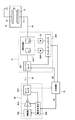
図1に、本発明の第1の実施形態におけるプラズマ処理装置の構成を示す。このプラズマ処理装置は、容量結合型(平行平板型)のプラズマエッチング装置として構成されており、たとえば表面がアルマイト処理(陽極酸化処理)されたアルミニウムからなる円筒形の真空チャンバ(処理容器)10を有している。チャンバ10は接地されている。
FIG. 1 shows a configuration of a plasma processing apparatus according to the first embodiment of the present invention. This plasma processing apparatus is configured as a capacitively coupled (parallel plate type) plasma etching apparatus. For example, a cylindrical vacuum chamber (processing vessel) 10 made of aluminum whose surface is anodized (anodized) is provided. Have. The
チャンバ10の底部には、セラミックなどの絶縁板12を介して円柱状のサセプタ支持台14が配置され、このサセプタ支持台14の上にたとえばアルミニウムからなるサセプタ16が設けられている。サセプタ16は下部電極を構成し、この上に被処理基板としてたとえば半導体ウエハWが載置される。
A
サセプタ16の上面には半導体ウエハWを保持するための静電チャック18が設けられている。この静電チャック18は導電膜からなる電極20を一対の絶縁層または絶縁シートの間に挟み込んだものであり、電極20にはスイッチ22を介して直流電源24が電気的に接続されている。直流電源24からの直流電圧により、半導体ウエハWを静電吸着力で静電チャック18に保持できるようになっている。静電チャック18の周囲でサセプタ16の上面には、エッチングの均一性を向上させるためのたとえばシリコンからなるフォーカスリング26が配置されている。サセプタ16およびサセプタ支持台14の側面にはたとえば石英からなる円筒状の内壁部材28が貼り付けられている。
An
サセプタ支持台14の内部には、たとえば円周方向に延びる冷媒室30が設けられている。この冷媒室30には、外付けのチラーユニット(図示せず)より配管32a,32bを介して所定温度の冷媒たとえば冷却水が循環供給される。冷媒の温度によってサセプタ16上の半導体ウエハWの処理温度を制御できるようになっている。さらに、伝熱ガス供給機構(図示せず)からの伝熱ガスたとえばHeガスが、ガス供給ライン34を介して静電チャック18の上面と半導体ウエハWの裏面との間に供給される。
Inside the
サセプタ16には、2系統の高周波給電部33,35が電気的に接続されている。第1系統の高周波給電部33は、プラズマの生成に適した一定の周波数fRF1(たとえば100MHz)の高周波RF1を出力する高周波電源36と、この高周波電源36からの高周波RF1をサセプタ16まで伝送する高周波伝送路43と、この高周波伝送路43上に設けられる整合器40とで構成されている。第2系統の高周波給電部35は、プラズマからサセプタ16上の半導体ウエハWへのイオンの引き込みに適した一定の周波数fRF2(たとえば13.56MHz)の高周波RF2を出力する高周波電源38と、この高周波電源38からの高周波RF2をサセプタ16まで伝送する高周波伝送路45と、この高周波伝送路45上に設けられる整合器42とで構成されている。サセプタ16の裏面(下面)に接続される給電用導体(たとえば給電棒)44は、両高周波伝送路43,45に共用される。
Two high-frequency
チャンバ10の天井には、サセプタ16と平行に向かいあって接地電位の上部電極46が設けられている。この上部電極46は、多数のガス噴出孔48aを有するたとえばSi、SiCなどのシリコン含有材質からなる電極板48と、この電極板48を着脱可能に支持する導電材料たとえば表面がアルマイト処理されたアルミニウムからなる電極支持体50とで構成されている。この上部電極46とサセプタ16との間にプラズマ生成空間または処理空間PSが形成されている。
An
電極支持体50は、その内部にガスバッファ室52を有するとともに、その下面にガスバッファ室52から電極板48のガス噴出孔48aに連通する多数のガス通気孔50aを有している。ガスバッファ室52にはガス供給管54を介して処理ガス供給源56が接続されている。ガス供給管54には、マスフローコントローラ(MFC)58および開閉バルブ60が設けられている。処理ガス供給源56より所定の処理ガス(エッチングガス)がガスバッファ室52に導入されると、電極板48のガス噴出孔48aよりサセプタ16上の半導体ウエハWに向けて処理空間PSに処理ガスがシャワー状に噴出されるようになっている。このように、上部電極46は、処理空間PSに処理ガスを供給するためのシャワーヘッドを兼ねている。
The
また、電極支持体50の内部には冷媒たとえば冷却水を流す通路(図示せず)も設けられており、外部のチラーユニットにより冷媒を介して上部電極46の全体、特に電極板48を所定温度に温調するようになっている。さらに、上部電極46に対する温度制御をより安定化させるために、電極支持体50の内部または上面にたとえば抵抗発熱素子からなるヒータ(図示せず)を取り付ける構成も可能である。
In addition, a passage (not shown) through which a coolant such as cooling water flows is provided inside the
サセプタ16およびサセプタ支持台14とチャンバ10の側壁との間に形成される環状の空間は排気空間となっており、この排気空間の底にはチャンバ10の排気口62が設けられている。この排気口62に排気管64を介して排気装置66が接続されている。排気装置66は、ターボ分子ポンプなどの真空ポンプを有しており、チャンバ10の室内、特に処理空間PSを所望の真空度まで減圧できるようになっている。また、チャンバ10の側壁には半導体ウエハWの搬入出口68を開閉するゲートバルブ70が取り付けられている。
An annular space formed between the susceptor 16 and the
主制御部72は、1つまたは複数のマイクロコンピュータを含み、外部メモリまたは内部メモリに格納されるソフトウェア(プログラム)およびレシピ情報にしたがって、装置内の各部、特に高周波電源36,38、整合器40,42、MFC58、開閉バルブ60、排気装置66等の個々の動作および装置全体の動作(シーケンス)を制御する。
The
また、主制御部72は、キーボード等の入力装置や液晶ディスプレイ等の表示装置を含むマン・マシン・インタフェース用の操作パネル(図示せず)および各種プログラムやレシピ、設定値等の各種データを格納または蓄積する外部記憶装置(図示せず)等とも接続されている。この実施形態では、主制御部72が1つの制御ユニットとして示されているが、複数の制御ユニットが主制御部72の機能を並列的または階層的に分担する形態を採ってもよい。
The
この容量結合型プラズマエッチング装置における枚葉ドライエッチングの基本的な動作は次のようにして行われる。先ず、ゲートバルブ70を開状態にして加工対象の半導体ウエハWをチャンバ10内に搬入して、静電チャック18の上に載置する。そして、処理ガス供給源56より処理ガスつまりエッチングガス(一般に混合ガス)を所定の流量および流量比でチャンバ10内に導入し、排気装置66による真空排気でチャンバ10内の圧力を設定値にする。さらに、高周波電源36からの高周波RF1(100MHz)と高周波電源38からの高周波RF2(13.56MHz)とを重畳して(あるいは単独で)サセプタ16に印加する。また、直流電源24より直流電圧を静電チャック18の電極20に印加して、半導体ウエハWを静電チャック18上に固定する。上部電極46のシャワーヘッドより吐出されたエッチングガスは両電極46,16間の高周波電界の下で放電し、処理空間PS内にプラズマが生成される。このプラズマに含まれるラジカルやイオンによって半導体ウエハWの主面の被加工膜がエッチングされる。
The basic operation of single wafer dry etching in this capacitively coupled plasma etching apparatus is performed as follows. First, the
この容量結合型プラズマエッチング装置においては、両高周波給電部33,35に対する主制御部72の制御により、チャンバ10内のサセプタ16に印加する高周波の種類、形態および組み合わせについて次のような7種類のRFモードを選択的に使用できるようになっている。このうち、第1〜第3のRFモードはパワー変調を用いず、第4〜第7のRFモードがパワー変調を用いる。
In this capacitively coupled plasma etching apparatus, the following seven types of high-frequency types, forms, and combinations applied to the
図2Aに示すように、第1のRFモードは、通常の下部2周波重畳方式であり、高周波給電部33の高周波RF1(100MHz)を設定上一定パワーの連続波(CW)とし、高周波給電部35の高周波RF2(13.56MHz)を設定上一定パワーの連続波(CW)とする。この場合、高周波RF1がプラズマの生成に支配的に作用または寄与し、高周波RF2がプラズマからサセプタ16上の半導体ウエハWへのイオンの引き込みに支配的に作用または寄与する。
As shown in FIG. 2A, the first RF mode is a normal lower two-frequency superposition method, and the high frequency RF1 (100 MHz) of the high frequency
第2のRFモードは、図2Bに示すように、高周波給電部33の高周波RF1を設定上一定パワーの連続波(CW)とし、高周波給電部35の高周波RF2を終始オフに保つ。この場合、高周波RF1は、プラズマの生成に作用するだけでなく、高周波RF2ほどの効き目はないがイオンの引き込みにも作用する。
In the second RF mode, as shown in FIG. 2B, the high frequency RF1 of the high frequency
第3のRFモードは、図2Cに示すように、高周波給電部33の高周波RF1を終始オフに保ち、高周波給電部35の高周波RF2を設定上一定パワーの連続波(CW)とする。この場合、高周波RF2は、イオンの引き込みに作用するだけでなく、高周波RF1ほど放電効率はよくないがプラズマの生成にも作用する。
In the third RF mode, as shown in FIG. 2C, the high-frequency RF1 of the high-frequency
図3Aに、第4のRFモードを示す。第4のRFモードは、高周波給電部33の高周波RF1をパワー変調によりパルス波形とし、高周波給電部35の高周波RF2を設定上一定パワーの連続波(CW)とする。この場合、高周波RF1がプラズマの生成に支配的に作用し、高周波RF2がイオンの引き込みに支配的に作用する。
FIG. 3A shows a fourth RF mode. In the fourth RF mode, the high frequency RF1 of the high frequency
図3Bに示す第5のRFモードは、高周波給電部33の高周波RF1をパワー変調によりパルス波形とし、高周波給電部35の高周波RF2を終始オフにする。この場合、高周波RF1は、プラズマの生成に作用するだけでなく、高周波RF2ほどの効き目はないがイオンの引き込みにも作用する。
In the fifth RF mode shown in FIG. 3B, the high frequency RF1 of the high frequency
図3Cに示す第6のRFモードは、高周波給電部33の高周波RF1を設定上一定パワーの連続波(CW)とし、高周波給電部35の高周波RF2をパワー変調によりパルス波形とする。この場合、主に高周波RF1がプラズマの生成に作用し、主に高周波RF2がイオンの引き込みに作用する。
In the sixth RF mode shown in FIG. 3C, the high frequency RF1 of the high frequency
最後に、第7のRFモードは、図3Dに示すように、高周波給電部33の高周波RF1を終始止めて、高周波給電部35の高周波RF2をパワー変調によりパルス波形とする。この場合、高周波RF2は、イオンの引き込みに作用するだけでなく、高周波RF1ほど放電効率はよくないがプラズマの生成にも作用する。
Finally, in the seventh RF mode, as shown in FIG. 3D, the high frequency RF1 of the high frequency
この実施形態のパワー変調においては、図3A〜図3Dに示すように、高周波RF1(RF2)のパワーがオン状態になるオン期間(第1の期間)Tonとオフ状態になるオフ期間(第2の期間)Toffとが一定のパルス周波数または周期TCで交互に繰り返す。オン期間Ton中のRFパワーは設定上一定である。主制御部72は、パワー変調のパルス周波数およびデューティ比を規定する変調制御パルス信号PSを高周波電源36(38)に与える。ここで、パルス周波数およびデューティ比の設定値をfs,DSとすると、TC=1/fS、TC=Ton+Toff、DS=Ton/(Ton+Toff)の関係式が成立する。
[実施形態1におけるパワー変調のデューティ制御法]
In the power modulation of this embodiment, as shown in FIGS. 3A to 3D, an on period (first period) T on in which the power of the high frequency RF1 (RF2) is turned on and an off period (first period) in which the power is turned off. (Period 2) T off repeats alternately at a constant pulse frequency or period T C. RF power during the on-time T on is the set constant. The
[Duty Control Method for Power Modulation in Embodiment 1]
次に、図4A〜図7Bにつき、第4〜第7のRFモードにおけるパワー変調のデューティ比制御を説明する。このデューティ比制御は、たとえば操作パネルを介してのレシピ上の設定あるいは別形式の設定にしたがい、各高周波給電部33,35に対する主制御部72の制御の1つとして行われる。すなわち、この実施形態では、主制御部72がデューティ比制御部を構成している。
Next, power modulation duty ratio control in the fourth to seventh RF modes will be described with reference to FIGS. 4A to 7B. This duty ratio control is performed as one of the controls of the
第4のRFモード(図3A)は、2種類のデューティ比制御法[4RFM−1,4RFM−2]を選択的に使用できるようになっている。図4Aおよび図4Bに示すように、第4のRFモードでは、プロセスを開始する際に、プラズマ生成用の高周波RF1(高周波給電部33)を時点t0で先に起動させ、一定時間Ta遅延後の時点t1でイオン引き込み用の高周波RF2(高周波給電部35)を起動させる。遅延時間Taは、高周波RF1の印加を開始してからプラズマが着火するまでの所要時間(通常0.2〜0.5秒)より大きな値(たとえば0.4〜0.8秒)に設定されるのが望ましい。 In the fourth RF mode (FIG. 3A), two types of duty ratio control methods [4RFM-1, 4RFM-2] can be selectively used. As shown in FIGS. 4A and 4B, in the first 4 RF mode, when starting the process, to activate RF power for plasma generation RF1 (the high-frequency power supply unit 33) earlier in time t 0, a predetermined time T a At time t 1 after the delay, the high-frequency RF 2 (high-frequency power feeding unit 35) for ion attraction is activated. Delay time T a is set to a value greater than the time required (typically 0.2 to 0.5 seconds) from the start of application of the high-frequency RF1 until plasma is ignited (e.g. 0.4 to 0.8 sec) It is desirable to be done.
ここで、第1のデューティ比制御法[4RFM−1]は、図4Aに示すように、パワー変調をかけられる高周波RF1のデューティ比を、プロセス開始時点t0では、実用上の任意のパワー変調条件(特にデューティ比、パルス周波数)の下でプラズマを確実に着火できる初期値(この実施例では90%)を用いる。なお、この初期値は、当該プロセス用の本来の設定値Dsに出来るだけ近い値が望ましい。すなわち、実用上の任意のパワー変調条件の下でプラズマを確実に着火できるデューティ比の範囲内でその下限値に近い値(通常85〜95%)が望ましい。 Here, in the first duty ratio control method [4RFM-1], as shown in FIG. 4A, the duty ratio of the high frequency RF1 that can be subjected to power modulation is set to any practical power modulation at the process start time t 0. An initial value (90% in this embodiment) that can reliably ignite the plasma under conditions (particularly duty ratio, pulse frequency) is used. The initial value is preferably a value as close as possible to the original set value D s for the process. That is, a value close to the lower limit (usually 85 to 95%) within the range of the duty ratio that can reliably ignite plasma under any practical power modulation condition is desirable.
そして、プロセスの開始と同時に高周波RF1のデューティ比を初期値90%から一定の負の勾配またはランプ波形で漸次的に下げ、所定時間Td(Td>Ta)を経過した時点t2で当該エッチングプロセス用の本来の設定値Dsまで下げる。時点t2以降は、プロセスの終了時(時点t4)までデューティ比を設定値Dsに固定または保持する。なお、高周波RF1,RF2を併用(重畳印加)する場合は、イオン引き込み用の高周波RF2をプロセス終了時より少し前(時点t3)に止める。この第1のデューティ比制御法[4RFM−1]は、第4のRFモードにおいてプラズマが着火しにくい場合、たとえばデューティ比Dsを低めに設定した場合、あるいはパルス周波数fsを高めに設定した場合に有効である。
Then, simultaneously with the start of the process, the duty ratio of the high frequency RF1 is gradually decreased from the
第2のデューティ比制御法[4RFM−2]は、図4Bに示すように、高周波RF1のデューティ比をプロセスの開始時(t0)から終了時(t4)まで終始本来の設定値Dsに固定する。このデューティ比制御法[4RFM−2]は、当該エッチングプロセス用に設定されたパワー変調のデューティ比Dsおよびパルス周波数fsの下でプラズマが確実に着火する場合には、好適に使える。 In the second duty ratio control method [4RFM-2], as shown in FIG. 4B, the duty ratio of the high frequency RF1 is set to the original set value D s from the start of the process (t 0 ) to the end of the process (t 4 ). Secure to. This duty ratio control method [4RFM-2] can be suitably used when the plasma is surely ignited under the power modulation duty ratio D s and pulse frequency f s set for the etching process.
第5のRFモード(図3B)も、2種類のデューティ比制御法[5RFM−1,5RFM−2]を選択的に使用できるようになっている。第5のRFモードでは、図5Aおよび図5Bに示すように、プロセスを開始する際に、プラズマ生成およびイオン引き込み兼用の高周波RF1(高周波給電部33)を時点t0で起動させる。 In the fifth RF mode (FIG. 3B), two kinds of duty ratio control methods [5RFM-1, 5RFM-2] can be selectively used. In a 5 RF mode, as shown in FIGS. 5A and 5B, when starting the process, to start plasma generation and ion attraction combined high-frequency RF1 (the high-frequency power supply unit 33) at time t 0.
ここで、第1のデューティ比制御法[5RFM−1]は、上述した第4のRFモードにおける第1のデューティ比制御法[4RFM−1]と同じシーケンスである。すなわち、図5Aに示すように、パワー変調をかけられる高周波RF1のデューティ比を、プロセス開始時点t0では、実用上の任意のパワー変調条件(特にデューティ比、パルス周波数)の下でプラズマを確実に着火できる初期値(90%)を用いる。そして、プロセスの開始と同時に高周波RF1のデューティ比を初期値90%から一定の負の勾配またはランプ波形で漸次的に下げ、所定時間Tdを経過した時点t2で当該エッチングプロセス用の本来の設定値Dsに合わせる。時点t2以降は、プロセスの終了時(時点t4)までデューティ比を設定値Dsに固定する。この第1のデューティ比制御法[5RFM−1]は、第5のRFモードにおいてプラズマが着火しにくい場合、たとえばデューティ比Dsを低めに設定した場合、あるいはパルス周波数fsを高めに設定した場合に有効である。
Here, the first duty ratio control method [5RFM-1] is the same sequence as the first duty ratio control method [4RFM-1] in the fourth RF mode described above. That is, as shown in FIG. 5A, the duty ratio of the high-
第5のRFモードにおける第2のデューティ比制御法[5RFM−2]も、上述した第4のRFモードにおける第2のデューティ比制御法[4RFM−2]と同じシーケンスになる。すなわち、図5Bに示すように、高周波RF1のデューティ比をプロセスの開始時(t0)から終了時(t4)まで終始本来の設定値Dsに固定する。当該エッチングプロセス用に設定されたパワー変調のデューティ比Dsおよびパルス周波数fsの下でプラズマが確実に着火する場合には、この第2のデューティ比制御法[5RFM−2]を好適に使用できる。 The second duty ratio control method [5RFM-2] in the fifth RF mode is the same sequence as the second duty ratio control method [4RFM-2] in the fourth RF mode. That is, as shown in FIG. 5B, the duty ratio of the high frequency RF1 is fixed to the original set value D s from the start (t 0 ) to the end (t 4 ) of the process. The second duty ratio control method [5RFM-2] is preferably used when the plasma is surely ignited under the power modulation duty ratio D s and pulse frequency f s set for the etching process. it can.
第6のRFモード(図3C)は、1種類のデューティ比制御法だけを用いる。図6に示すように、第6のRFモードでは、プロセスを開始する際に、プラズマ生成用の高周波RF1(高周波給電部33)を時点t0で先に起動させ、一定時間Ta遅延後の時点t1でイオン引き込み用の高周波RF2(高周波給電部35)を起動させる。この場合、高周波RF1はデューティ比100%に相当する連続波(CW)であるため、圧力やRF1のパワーが通常の値に設定されている限り、高周波RF2側でパワー変調のデューティ比Dsおよびバルス周波数fsが如何なる値に設定されても、チャンバ10内でプラズマは確実に着火する。
The sixth RF mode (FIG. 3C) uses only one type of duty ratio control method. As shown in FIG. 6, in the first 6 RF mode, when starting the process, for plasma generation high frequency RF1 starts a (high-frequency power supply unit 33) earlier in time t 0, after a certain time T a delay At the time t 1 , the high frequency RF 2 (high frequency power supply unit 35) for ion attraction is activated. In this case, since the high frequency RF1 is a continuous wave (CW) corresponding to a duty ratio of 100%, as long as the pressure and the power of the RF1 are set to normal values, the duty ratio D s of power modulation on the high frequency RF2 side and Regardless of the value of the pulse frequency f s , the plasma is surely ignited in the
そこで、第6のRFモードにおけるデューティ比制御法[6RFM]は、高周波RF2のデューティ比を高周波RF2(高周波給電部35)の起動時(t1)から停止時(t3)まで終始設定値Dsに固定する。 Therefore, the duty ratio control method [6RFM] in the sixth RF mode sets the duty ratio of the high frequency RF2 from the start time (t 1 ) to the stop time (t 3 ) of the high frequency RF 2 (high frequency power supply unit 35). Fix to s .
第7のRFモード(図3D)は、2種類のデューティ比制御法[7RFM−1,7RFM−2]を選択的に使用できるようになっている。第7のRFモードでは、図7Aおよび図7Bに示すように、プロセスを開始する際に、プラズマ生成およびイオン引き込み兼用の高周波RF2(高周波給電部35)を時点t0で起動させる。 In the seventh RF mode (FIG. 3D), two types of duty ratio control methods [7RFM-1, 7RFM-2] can be selectively used. In the seventh RF mode, as shown in FIGS. 7A and 7B, when the process is started, the high-frequency RF 2 (high-frequency power feeding unit 35) that is used for both plasma generation and ion attraction is activated at time t 0 .
ここで、第1のデューティ比制御法[7RFM−1]は、図7Aに示すように、パワー変調をかけられる高周波RF2のデューティ比を、プロセス開始時点t0では、実用上の如何なるパワー変調条件(特にデューティ比、パルス周波数)の下でプラズマを確実に着火できる初期値(90%)に合わせる。そして、プロセス開始直後に、高周波RF2のデューティ比を初期値90%から一定の負の勾配またはランプ波形で漸次的に下げ、所定時間Tdを経過した時点t2で当該エッチングプロセス用の本来の設定値Dsに合わせる。時点t2以降は、プロセスの終了時(時点t4)までデューティ比を設定値Dsに固定する。第7のRFモードにおいてプラズマが着火しにくい場合、たとえばエッチングプロセス用のデューティ比Dsを低めに設定した場合、あるいはパルス周波数fsを高めに設定した場合には、この第1のデューティ比制御法[7RFM−1]を好適に使用できる。
Here, in the first duty ratio control method [7RFM-1], as shown in FIG. 7A, the duty ratio of the high-frequency RF 2 that can be subjected to power modulation is set to any practical power modulation condition at the process start time t 0. It is set to an initial value (90%) at which the plasma can be reliably ignited under (especially duty ratio, pulse frequency). Immediately after the start of the process, the duty ratio of the high-frequency RF 2 is gradually lowered from the
第2のデューティ比制御法[7RFM−2]は、図7Bに示すように、高周波RF1のデューティ比をプロセスの開始時(t0)から終了時(t4)まで終始本来の設定値Dsに固定する。当該エッチングプロセス用に設定されたパワー変調のデューティ比Dsおよびパルス周波数fsの下でプラズマが確実に着火する場合には、このデューティ比制御法[7RFM−2]を好適に使える。 In the second duty ratio control method [7RFM-2], as shown in FIG. 7B, the duty ratio of the high-frequency RF1 is set to the original set value D s from the start (t 0 ) to the end (t 4 ) of the process. Secure to. This duty ratio control method [7RFM-2] can be preferably used when the plasma is surely ignited under the power modulation duty ratio D s and pulse frequency f s set for the etching process.
上記のように、この実施形態では、第4、第5および第7のRFモードにおいてプラズマが着火しにくい場合に、図4A、図5Aおよび図7Aに示すように、パワー変調のデューティ比をプラズマ着火用の初期値(90%値)で開始し、所定の遷移時間Tdをかけて初期値から当該エッチングプロセス用の設定値Dsまでランプ波形で漸次的に下げるようにしている。ここで、遷移時間Tdは、短すぎると整合器40(42)内の整合動作が不安定になり、長すぎると当該エッチングプロセスのプロセス特性またはプロセス結果に影響が生じる。したがって、長短両面で制限があり、通常はTd=0.5〜3.0秒に選定される。
[実施形態1におけるプラズマ着火性に関する効果]
As described above, in this embodiment, when the plasma is difficult to ignite in the fourth, fifth, and seventh RF modes, the duty ratio of the power modulation is changed to plasma as shown in FIGS. 4A, 5A, and 7A. It starts with an initial value for ignition (90% value), and gradually decreases in a ramp waveform from the initial value to the set value D s for the etching process over a predetermined transition time T d . Here, if the transition time Td is too short, the matching operation in the matching unit 40 (42) becomes unstable, and if it is too long, the process characteristics or the process result of the etching process is affected. Therefore, there are limitations on both long and short sides, and usually T d = 0.5 to 3.0 seconds is selected.
[Effects on plasma ignitability in Embodiment 1]
次に、この実施形態において、上記第5のRFモードにおける第1のデューティ比制御法[5RFM−1](図5A)のプラズマ着火性に関する検証実験について説明する。 Next, in this embodiment, a verification experiment regarding the plasma ignitability of the first duty ratio control method [5RFM-1] (FIG. 5A) in the fifth RF mode will be described.
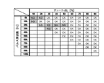
本発明者は、チャンバ内圧力2666Pa(20mTorr)、RF1パワー300W、RF2パワー0W、エッチングガスC4F8/O2/Ar(24/16/150sccm)、電極間ギャップ22mmを主たるプロセス条件とする第5のRFモードによるプラズマエッチングの実験において、第2のデューティ比制御法[5RFM−2]を使用し、その中で高周波RF1にかけるパルス変調のデューティ比Dsおよびパルス周波数fsをパラメータとしてそれぞれDs=10%〜90%、fs=5〜90kHzで可変し、各パラメータ値(Ds,fs)の組み合わせにおけるプラズマ着火性を評価した。図8は、デューティ設定値Dsを低め(たとえば10%)に選んで第2のデューティ比制御法[5RFM−2]を用いた場合のシーケンスを示す。
The inventor has the main process conditions of a chamber internal pressure of 2666 Pa (20 mTorr), an RF1 power of 300 W, an RF2 power of 0 W, an etching gas C 4 F 8 / O 2 / Ar (24/16/150 sccm), and an interelectrode gap of 22 mm. In the experiment of plasma etching in the fifth RF mode, the second duty ratio control method [5RFM-2] is used, and the pulse modulation duty ratio D s and pulse frequency f s applied to the
図9Aに、第2のデューティ比制御法[5RFM−2]を用いた場合の実験結果を示す。この図の表(マトリクス)において、縦方向の欄はデューティ設定値Dsのパラメータ値を示し、横方向の欄はパルス周波数fsのパラメータ値を示す。「OK」の表記は、このセルに対応するパラメータ値(Ds,fs)を用いたプロセスではプラズマが着火しかつ安定に持続したことを表わす。「NG」の表記は、このセルに対応するパラメータ値(Ds,fs)を用いたプロセスではプラズマが着火しなかったか、あるいは着火しても安定しなかったことを表わす。空欄は、このセルに対応するパラメータ値(Ds,fs)を用いたプロセスの実験は行われなかったことを示す。 FIG. 9A shows an experimental result when the second duty ratio control method [5RFM-2] is used. In the table (matrix) of this figure, the vertical column indicates the parameter value of the duty set value D s , and the horizontal column indicates the parameter value of the pulse frequency f s . The notation “OK” indicates that the plasma was ignited and stably maintained in the process using the parameter values (D s , f s ) corresponding to this cell. The notation “NG” indicates that the plasma did not ignite in the process using the parameter values (D s , f s ) corresponding to this cell, or that the plasma did not stabilize even when ignited. A blank column indicates that the process experiment using the parameter values (D s , f s ) corresponding to this cell was not performed.
図示のように、パラメータ値(Ds,fs)が(40kHz、40%),(40kHz、50%),(40kHz、60%),(40kHz、70%),(40kHz、80%),(50kHz、70%),(50kHz、80%),(60kHz、60%),(60kHz、70%),(70kHz、70%)の各場合に、「NG」(プラズマ未着火・安定せず)の実験結果が得られた。他のパラメータ値(Ds,fs)の組み合わせではいずれも「OK」(プラズマ着火・安定)の実験結果が得られた。 As shown, the parameter values (D s , f s ) are (40 kHz, 40%), (40 kHz, 50%), (40 kHz, 60%), (40 kHz, 70%), (40 kHz, 80%), In each case of (50 kHz, 70%), (50 kHz, 80%), (60 kHz, 60%), (60 kHz, 70%), (70 kHz, 70%), “NG” (plasma not ignited / not stable) ) Experimental results were obtained. For all other combinations of parameter values (D s , f s ), an “OK” (plasma ignition / stable) experimental result was obtained.
本発明者は、第2のデューティ比制御法[5RFM−2]の下で「NG」の実験結果が出たパラメータ値(Ds,fs)の各場合について、第1のデューティ比制御法[5RFM−1]を使用し、上記と同じプロセス条件でプラズマエッチングの実験を行い、プラズマ着火性を評価した。 The inventor provides the first duty ratio control method for each case of the parameter values (D s , f s ) for which the experimental result of “NG” is obtained under the second duty ratio control method [5RFM-2]. Using [5RFM-1], an experiment of plasma etching was performed under the same process conditions as described above, and plasma ignitability was evaluated.
その結果、図9Bに示すように、パラメータ値(Ds,fs)が(40kHz、40%),(40kHz、50%),(40kHz、60%),(40kHz、70%),(40kHz、80%),(50kHz、70%),(50kHz、80%),(60kHz、60%),(60kHz、70%),(70kHz、70%)の各場合でいずれも「OK」(プラズマ着火・安定)であった。 As a result, as shown in FIG. 9B, the parameter values (D s , f s ) are (40 kHz, 40%), (40 kHz, 50%), (40 kHz, 60%), (40 kHz, 70%), (40 kHz , 80%), (50 kHz, 70%), (50 kHz, 80%), (60 kHz, 60%), (60 kHz, 70%), (70 kHz, 70%). Ignition / Stable).
なお、この実験で用いた遷移時間Tdはいずれの場合も1.0秒であった。図9Bにおける「1.0s」の表記はそのことを表わしている。また、図9Bの「OK」の表記は、図9Aと同じであり、このセルに対応するパラメータ値(Ds,fs)を用いたプロセスでは第2のデューティ比制御法[5RFM−2]の下で「OK」の結果が得られたことを表わしている。 Note that the transition time Td used in this experiment was 1.0 seconds in all cases. The notation “1.0 s” in FIG. 9B represents this. The notation “OK” in FIG. 9B is the same as that in FIG. 9A. In the process using the parameter values (D s , f s ) corresponding to this cell, the second duty ratio control method [5RFM-2] Represents that an “OK” result was obtained.
本発明者は、別の実験として、チャンバ内圧力、RF1/RF2パワー、エッチングガスの各条件は上記と同じで、電極間ギャップを30mmに変更した第5のRFモードのプラズマエッチングの実験において、上記と同様に第2のデューティ比制御法[5RFM−2]を使用し、その中で高周波RH1にかけるパルス変調のデューティ比Dsおよびパルス周波数fsをパラメータとしてそれぞれDs=10%〜90%、fs=5〜90kHzで可変し、各パラメータ値(Ds,fs)の組み合わせにおけるプラズマ着火性を評価した。 As another experiment, the present inventor conducted a fifth RF mode plasma etching experiment in which the chamber pressure, RF1 / RF2 power, and etching gas conditions were the same as described above, and the gap between the electrodes was changed to 30 mm. Similarly to the above, the second duty ratio control method [5RFM-2] is used, and among them, the duty ratio D s of pulse modulation applied to the high frequency RH1 and the pulse frequency f s are parameters D s = 10% to 90%, respectively. %, F s = 5 to 90 kHz, and plasma ignitability in each combination of parameter values (D s , f s ) was evaluated.
その結果、図10Aに示すように、パラメータ値(Ds,fs)が(5kHz、10%),(5kHz、20%),(10kHz、10%),(20kHz、20%),(20kHz、30%),(20kHz、40%),(20kHz、40%),(30kHz、30%)の各場合で「NG」であった。他のパラメータ値(Ds,fs)の組み合わせではいずれも「OK」であった。 As a result, as shown in FIG. 10A, the parameter values (D s , f s ) are (5 kHz, 10%), (5 kHz, 20%), (10 kHz, 10%), (20 kHz, 20%), (20 kHz , 30%), (20 kHz, 40%), (20 kHz, 40%), and (30 kHz, 30%). All combinations of other parameter values (D s , f s ) were “OK”.
本発明者は、上記実験結果を踏まえ、第2のデューティ比制御法[5RFM−2]の下で「NG」であったパラメータ値(Ds,fs)の各場合について、第1のデューティ比制御法[5RFM−1]を使用し、上記と同一プロセス条件でプラズマエッチングの実験を行い、プラズマ着火性を評価した。 Based on the above experimental results, the present inventor has obtained the first duty for each parameter value (D s , f s ) that was “NG” under the second duty ratio control method [5RFM-2]. Using a ratio control method [5RFM-1], an experiment of plasma etching was performed under the same process conditions as described above, and plasma ignitability was evaluated.
その結果、図10Bに示すように、パラメータ値(Ds,fs)が(5kHz、10%),(5kHz、20%),(10kHz、10%),(20kHz、20%),(20kHz、30%),(20kHz、40%),(20kHz、50%),(30kHz、30%)の各場合でいずれも「OK」(プラズマ着火・安定)であった。 As a result, as shown in FIG. 10B, the parameter values (D s , f s ) are (5 kHz, 10%), (5 kHz, 20%), (10 kHz, 10%), (20 kHz, 20%), (20 kHz , 30%), (20 kHz, 40%), (20 kHz, 50%), and (30 kHz, 30%), all were “OK” (plasma ignition / stable).
この実験で用いた遷移時間Tdは、パラメータ値(Ds,fs)が(5kHz、10%),(5kHz、20%)のときは2.5秒、(10kHz、10%)のときは1.5秒、(20kHz、20%),(20kHz、30%),(20kHz、40%),(20kHz、40%),(30kHz、30%)のときは1.0秒であった。図10Bにおける「2.5s」、「1.5s」、「1.0s」の表記はそのことを表わしている。また、図10Bにおいても、「OK」の表記は、このセルに対応するパラメータ値(Ds,fs)では第2のデューティ比制御法[5RFM−2]の下で「OK」の結果が出たことを表わしている。 The transition time T d used in this experiment is 2.5 seconds when the parameter value (D s , f s ) is (5 kHz, 10%), (5 kHz, 20%), and (10 kHz, 10%). Was 1.5 seconds, (20 kHz, 20%), (20 kHz, 30%), (20 kHz, 40%), (20 kHz, 40%), (30 kHz, 30%) was 1.0 second. . The notations “2.5 s”, “1.5 s”, and “1.0 s” in FIG. 10B indicate that. Also in FIG. 10B, the notation “OK” indicates that the parameter value (D s , f s ) corresponding to this cell indicates that the result of “OK” is under the second duty ratio control method [5RFM-2]. Indicates that it has gone out.
上記のように、上記第5のRFモードにおいては、第2のデューティ比制御法[5RFM−2]の下でプラズマを確実に着火できる場合は、パワー変調のデューティ比をプロセスの開始から設定値Dsに固定する第2のデューティ比制御法[5RFM−2]を使用するのが望ましい。しかし、第2のデューティ比制御法[5RFM−2]の下でプラズマを確実に着火できない場合は、所望のプロセス条件によるプラズマプロセスを安定確実に実施するうえで、パワー変調のデューティ比をプロセス開始直後にランプ低減する第1のデューティ比制御法[5RFM−1]を使用するのが好ましい。 As described above, in the fifth RF mode, when the plasma can be reliably ignited under the second duty ratio control method [5RFM-2], the power modulation duty ratio is set to the set value from the start of the process. It is desirable to use the second duty ratio control method [5RFM-2] that is fixed to D s . However, if the plasma cannot be ignited reliably under the second duty ratio control method [5RFM-2], the power modulation duty ratio is started in order to stably perform the plasma process under the desired process conditions. It is preferable to use the first duty ratio control method [5RFM-1] that immediately reduces the lamp.
同様に、上記第4のRFモードにおいて、第2のデューティ比制御法[4RFM−2]の下でプラズマを確実に着火できる場合は、パワー変調のデューティ比をプロセスの開始から設定値Dsに固定する第2のデューティ比制御法[4RFM−2]を使用するのが望ましい。しかし、第2のデューティ比制御法[4RFM−2]の下でプラズマを確実に着火できない場合は、所望のプロセス条件によるプラズマプロセスを安定確実に実施するうえで、パワー変調のデューティ比をプロセス開始直後にランプ低減する第1のデューティ比制御法[4RFM−1]を使用するのが好ましい。 Similarly, in the fourth RF mode, when the plasma can be reliably ignited under the second duty ratio control method [4RFM-2], the power modulation duty ratio is changed from the start of the process to the set value D s . It is desirable to use the fixed second duty ratio control method [4RFM-2]. However, if the plasma cannot be ignited reliably under the second duty ratio control method [4RFM-2], the power modulation duty ratio is started to stably perform the plasma process under the desired process conditions. It is preferable to use the first duty ratio control method [4RFM-1] that immediately reduces the lamp.
また、上記第7のRFモードにおいても、第2のデューティ比制御法[7RFM−2]の下でプラズマを確実に着火できる場合は、パワー変調のデューティ比をプロセスの開始から設定値Dsに固定する第2のデューティ比制御法[7RFM−2]を使用するのが望ましい。しかし、第2のデューティ比制御法[7RFM−2]の下でプラズマを確実に着火できない場合は、所望のプロセス条件によるプラズマプロセスを安定確実に実施するうえで、パワー変調のデューティ比をプロセス開始直後でランプ低減する第1のデューティ比制御法[7RFM−1]を使用するのが好ましい。
[実施形態1における高周波給電部の構成及び作用]
Also in the seventh RF mode, if the plasma can be ignited reliably under the second duty ratio control method [7RFM-2], the power modulation duty ratio is changed to the set value D s from the start of the process. It is desirable to use the fixed second duty ratio control method [7RFM-2]. However, if the plasma cannot be ignited reliably under the second duty ratio control method [7RFM-2], the power modulation duty ratio is started in order to stably perform the plasma process under the desired process conditions. It is preferable to use the first duty ratio control method [7RFM-1] that immediately reduces the lamp.
[Configuration and Action of High Frequency Power Supply Unit in Embodiment 1]
図11に、この実施形態における高周波給電部33の構成、特に高周波電源36および整合器40の構成を示す。
In FIG. 11, the structure of the high frequency electric
高周波電源36は、プラズマの生成に適した周波数(たとえば100MHz)の正弦波を発生する発振器80Aと、この発振器80Aより出力される正弦波のパワーを可変の利得または増幅率で増幅するパワーアンプ82Aと、主制御部72からの制御信号にしたがって発振器80Aおよびパワーアンプ82Aを直接制御する電源制御部84Aとを備えている。主制御部72から電源制御部84Aには、上記変調制御パルス信号PSだけでなく、通常の電源オン・オフやパワーインターロック関係等の制御信号およびパワー設定値等のデータも与えられる。主制御部72と電源制御部84Aは、高周波RF1系のパワー変調部を構成する。
The high-
高周波電源36のユニット内には、RFパワーモニタ86Aも備わっている。このRFパワーモニタ86Aは、図示省略するが、方向性結合器、進行波パワーモニタ部および反射波パワーモニタ部を有している。ここで、方向性結合器は、高周波伝送路43上を順方向に伝搬するRFパワー(進行波)と逆方向に伝搬するRFパワー(反射波)のそれぞれに対応する信号を取り出す。進行波パワーモニタ部は、方向性結合器により取り出された進行波パワー検出信号を基に、高周波伝送路43上の進行波に含まれる基本波進行波(100MHz)のパワーを表わす信号を生成する。この信号つまり基本波進行波パワー測定値信号は、パワーフィードバック制御用に高周波電源36内の電源制御部84Aに与えられるとともに、モニタ表示用に主制御部72にも与えられる。反射波パワーモニタ部は、チャンバ10内のプラズマから高周波電源36に返ってくる反射波に含まれる基本波反射波(100MHz)のパワーを測定するとともに、チャンバ10内のプラズマから高周波電源36に返ってくる反射波に含まれる全ての反射波スペクトルのトータルのパワーを測定する。反射波パワーモニタ部により得られる基本波反射波パワー測定値はモニタ表示用に主制御部72に与えられ、トータル反射波パワー測定値はパワーアンプ保護用のモニタ値として高周波電源36内の電源制御部84Aに与えられる。
In the unit of the high
整合器40は、複数たとえば2つの可変リアクタンス素子(たとえば可変コンデンサあるいは可変リアクトル)XH1,XH2を含む整合回路88Aと、可変リアクタンス素子XH1,XH2のリアクタンスをアクチエータたとえばステッピングモータ(M)90A,92Aを介して可変するマッチングコントローラ94Aと、高周波給電ライン43上で整合回路88Aのインピーダンスを含む負荷側のインピーダンスを測定するインピーダンスセンサ96Aとを有している。
The matching
マッチングコントローラ94Aは、主制御部72の制御の下で動作し、インピーダンスセンサ96Aより与えられる負荷側インピーダンス測定値をフィードバック信号として、負荷側インピーダンス測定値が高周波電源36側のインピーダンスに相当する整合ポイント(通常50Ω)に一致ないし近似するように、可変リアクタンス素子XH1,XH2のリアクタンスをモータ90A,92Aの駆動制御を通じて可変するようになっている。
The matching
インピーダンスセンサ96Aは、図示省略するが、高周波伝送路43上のRF電圧およびRF電流をそれぞれ検出するRF電圧検出器およびRF電流検出器と、RF電圧検出器およびRF電流検出器よりそれぞれ得られるRF電圧検出値およびRF電流検出値から負荷側のインピーダンスの測定値を演算する負荷インピーダンス測定値演算部とを有している。
Although not shown, the
この実施形態において、高周波RF1にパワー変調をかけるときは、図13に示すように、パルス周波数の各サイクル毎にオン期間Ton内に設けられるモニタ時間(負荷側インピーダンス測定時間)THを指示するモニタ信号ASが、主制御部72よりインピーダンスセンサ96Aに与えられる。好ましくは、図13に示すように、高周波伝送路43上でRF1系の反射波のパワーが突発的に増大するオン期間Tonの開始直後および終了直前の過渡時間TA1,TA2を除いた区間にモニタ時間THが設定される。高周波RF1がパルス周波数fsでオン・オフしても、モニタ時間THがオン期間Ton内だけに設定され、オフ期間Toff内には設定されないので、整合器40からはあたかも高周波RF1がオンし続けている連続波(CW)のように見える。
In this embodiment, when applying power modulation to a high frequency RF1, as shown in FIG. 13, the monitor is provided in the on-period T on each cycle of the pulse frequency time (load impedance measurement time) instructed T H The monitor signal AS to be transmitted is supplied from the
インピーダンスセンサ96Aは、モニタ信号ASによって指示されるモニタ時間THの間だけ負荷側インピーダンス測定の動作を行う。したがって、インピーダンスセンサ96Aよりマッチングコントローラ94Aに与えられる負荷側インピーダンス測定値は、パワー変調に同期してパルス周波数fsの各サイクル毎に更新される。マッチングコントローラ94Aは、この更新の合間にも、整合動作つまりリアクタンス素子XH1,XH2のリアクタンス可変制御を停止することなく、更新直前の負荷側インピーダンス測定値を整合ポイントに一致ないし近似させるように、ステッピングモータ90A,92Aを連続的に駆動制御する。
この実施形態では、主制御部72が、整合器40に対してモニタ時間制御部の機能を有し、高周波RF1のパワー変調におけるデューティ比の変化に連動してモニタ時間THを比例制御する。すなわち、図13に示すように、プロセスの開始直後でパワー変調のデューティ比が漸次的に低減する際に、これに比例してモニタ時間THを漸次的に低減する。
In this embodiment, the
図12に、この実施形態における高周波給電部35の構成を示す。高周波給電部35の高周波電源38および整合器42は、そこで扱う高周波RF2の周波数(13.56MHz)が上記高周波RF1の周波数(100MHz)と異なるだけで、上述した高周波給電部33の高周波電源36および整合器40とそれぞれ同様の構成および機能を有している。すなわち、高周波電源38の発振器80Bがイオンの引き込みに適した周波数(たとえば13.56MHz)の正弦波を発生する点を除けば、高周波電源38および整合器42内の各部は高周波電源36および整合器40内の対応する各部と同様の構成および機能を有している。したがって、たとえば電源制御部84Bは、主制御部72と協働して高周波RF2系のパワー変調部を構成する。
FIG. 12 shows a configuration of the high-frequency
もっとも、高周波電源38内の電源制御部84Bおよび整合器42内のインピーダンスセンサ96Bには、主制御部72より高周波給電部33向けとは独立に変調制御パルス信号PCおよびモニタ信号BSがそれぞれ与えられる。
However, the modulation control pulse signal PC and the monitor signal BS are respectively supplied from the
すなわち、高周波RF2にパワー変調をかけるときは、図13に示すように、パルス周波数の各サイクル毎にオン期間Ton内に設けられるモニタ時間(負荷側インピーダンス測定時間)TLを指示するモニタ信号BSが、主制御部72よりインピーダンスセンサ96Bに与えられる。好ましくは、図13に示すように、高周波伝送路45上でRF2系の反射波のパワーが突発的に増大するオン期間Tonの開始直後および終了直前の過渡時間TB1,TB2を除いた区間にモニタ時間TLが設定される。高周波RF2がパルス周波数fsでオン・オフしても、モニタ時間TLがオン期間Ton内だけに設定され、オフ期間Toff内には設定されないので、整合器42からはあたかも高周波RF2がオンし続けている連続波(CW)のように見える。
That is, when applying a power modulation to a high frequency RF2, as shown in FIG. 13, the monitor is provided in the on-period T on each cycle of the pulse frequency time (load impedance measurement time) Monitor signal instructing T L BS is supplied from the
インピーダンスセンサ96Bは、モニタ信号BSによって指示されるモニタ時間TLの間だけ負荷側インピーダンス測定の動作を行う。したがって、インピーダンスセンサ96Bよりマッチングコントローラ94Bに与えられる負荷側インピーダンス測定値は、パワー変調に同期してパルス周波数の各サイクル毎に更新される。マッチングコントローラ94Bは、この更新の合間にも、整合動作つまりリアクタンス素子XL1,XL2のリアクタンス可変制御を停止することなく、更新直前の負荷側インピーダンス測定値を整合ポイントに一致ないし近似させるように、ステッピングモータ90B,92Bを連続的に駆動制御する。
The
主制御部72は、整合器42に対するモニタ時間制御部として機能し、高周波RF2のパワー変調におけるデューティ比に連関してそれに比例するようにモニタ時間TLを制御する。すなわち、図13に示すように、プロセスの開始直後でパワー変調のデューティ比が漸次的に低減する際に、これに比例してモニタ時間TLを漸次的に低減する。
The
本発明者は、整合動作に関して上記第5のRFモードにおける第1のデューティ比制御法[5RFM−1](図5A)およびモニタ時間制御法(図13)の効果を上記と同様のプロセス条件によるプラズマエッチングの実験で検証した。この実験では、整合器40の整合回路88Aに含まれる2つの可変リアクタンス素子XH1,XH2に可変コンデンサRF1C1,RF1C2をそれぞれ使用した。
The inventor has obtained the effects of the first duty ratio control method [5RFM-1] (FIG. 5A) and the monitor time control method (FIG. 13) in the fifth RF mode with respect to the matching operation under the same process conditions as described above. It verified by the experiment of plasma etching. In this experiment, variable capacitors RF 1 C 1 and RF 1 C 2 were used for the two variable reactance elements X H1 and X H2 included in the
図14に、上記実施例の実験で観測された各部の波形を示す。図示のように、可変コンデンサRF1C1のステップ(キャパシタンス・ポジション)は、プロセス開始直後に初期値からオーバーシュート気味で立ち上がる。そして、遷移期間Td(2.5秒)中に落ち着いたRF1C1のステップ(キャパシタンス・ポジション)は、その後も、つまりデューティ比を設定値Ds(30%)に固定してからも、略一定に保たれた。また、可変コンデンサRF1C2のステップ(キャパシタンス・ポジション)は、プロセス開始直後に初期値からステップ状に立ち下がる。そして、遷移期間Td中に落ち着いたRF1C2のステップ(キャパシタンス・ポジション)は、その後も、つまりデューティ比を設定値Ds(30%)に固定してからも、略一定に保たれた。高周波伝送路42上の反射波パワーRF1Prは、プロセス開始直後にインパルス状に発生するものの、遷移期間Td中に収まり、以後殆ど発生しなかった。このように、上記実施例の実験では、遷移期間Tdの中盤からプロセスが終了するまで高周波伝送路43上でインピーダンス整合が良好にとれていたことが確認された。
FIG. 14 shows waveforms of respective parts observed in the experiment of the above embodiment. As shown in the figure, the step (capacitance position) of the variable capacitor RF 1 C 1 rises from the initial value with an overshoot immediately after the start of the process. Then, the RF 1 C 1 step (capacitance position) settled during the transition period T d (2.5 seconds) continues after that, that is, after the duty ratio is fixed to the set value D s (30%). , Kept almost constant. Further, the step (capacitance position) of the variable capacitor RF 1 C 2 falls in a step shape from the initial value immediately after the start of the process. Then, the step (capacitance position) of RF 1 C 2 settled during the transition period T d is kept substantially constant thereafter, that is, even after the duty ratio is fixed to the set value D s (30%). It was. Reflection wave power RF 1 P r on the high-
本発明者は、比較例として、図15に示すように、プロセス開始直後に上記実施例の遷移期間Tdに相当する立ち上げ期間Te(2.5秒)は高周波RF1を連続波(デューティ比100%に相当)とし、立ち上げ期間Te経過時に設定デューティ比Ds(30%)のパワー変調に切り換えるデューティ比制御法を用いて、上記実施例と同じプロセス条件によるプラズマエッチングの実験を行った。
As a comparative example, the inventor, as shown in FIG. 15, immediately after the start of the process, the start-up period T e (2.5 seconds) corresponding to the transition period T d of the above-described embodiment is a high-
図16に、上記比較例の実験で観測された各部の波形を示す。図示のように、立ち上げ期間Te中の各部の波形は、上記実施例の場合と殆ど同じである。また、この比較例でも、実施例と同様のモニタ信号AS(パルス周波数の各サイクル毎にオン時間Ton内のモニタ時間THを指示する信号)を主制御部72より整合器40のインピーダンスセンサ96Aに与えた。しかし、立ち上げ期間Teの後、つまり高周波RF1を連続波(CW)からパワー変調のパルスに切り換えた後(時点t2以降)の各部の波形は、高周波伝送路43上の進行波パワーRF1Ptを除き、上記実施例の場合とは著しく異なる。
FIG. 16 shows waveforms of respective parts observed in the experiment of the comparative example. As shown, the waveform of each part in the start-up period T e, is almost the same as in the above embodiment. Also in this comparative example, the impedance sensor of Example similar to the monitor signal AS matching
すなわち、可変コンデンサRF1C1のステップ(キャパシタンス・ポジション)は、切り換え(t2)の直後に初期値の方へ逆戻りし、しかもプロセス終了時まで大きなハンチングを起こし続けた。可変コンデンサRF1C2のステップ(キャパシタンス・ポジション)も、切り換え(t2)の直後に初期値の方へ逆戻りし、RF1C1ほどではないがプロセスの終了までハンチングを起こし続けた。一方、高周波伝送路43上の反射波パワーRF1Prは、切り換え(t2)の直後にステップ状に大きく増大し、プロセスの終了まで減少しなかった。このように、上記比較例の実験では、インピーダンスセンサのモニタ時間をパルス周波数の各サイクルのオン時間内に限定する整合モニタ法を用いたとしても、高周波RF1を連続波(CW)からパワー変調のパルスに切り換えるとその後はプロセスが終了するまで高周波伝送路43上でインピーダンス整合が全くとれていなかったことが確認された。
That is, the step (capacitance position) of the variable capacitor RF 1 C 1 returned to the initial value immediately after the switching (t 2 ) and continued to cause a large hunting until the end of the process. The step (capacitance position) of the variable capacitor RF 1 C 2 also returned to the initial value immediately after switching (t 2 ) and continued to cause hunting until the end of the process, although not as much as RF 1 C 1 . On the other hand, the reflected wave power RF 1 P r on the high-
なお、上記比較例における整合不良(図16)は、連続波(CW)の時とパワー変調をかけた時とでプラズマ負荷のインピーダンスが大きく異なる場合であり、概してパワー変調のデューティ比が低いときに起こりやすい。しかし、デューティ比が低くても、圧力等の他の条件次第でプラズマ負荷インピーダンスの差(変動)が小さいときは、そのような整合不良に至らないこともある。いずれにして本発明のデューティ比制御法を用いることによって上記比較例のような整合不良を解消することができる。
[実施形態2におけるプラズマ処理装置の構成及び作用]
In addition, the poor alignment (FIG. 16) in the comparative example is when the impedance of the plasma load is greatly different between the continuous wave (CW) and the power modulation, and generally when the duty ratio of the power modulation is low. Easy to happen. However, even if the duty ratio is low, such a misalignment may not occur if the difference (fluctuation) in plasma load impedance is small depending on other conditions such as pressure. In any case, by using the duty ratio control method of the present invention, the alignment failure as in the comparative example can be eliminated.
[Configuration and Operation of Plasma Processing Apparatus in Embodiment 2]
図17に、本発明の第2の実施形態におけるプラズマ処理装置の構成を示す。図中、上記第1の実施形態におけるプラズマ処理装置(図1)と同様構成または機能を有する部分には同一の符号を付している。 FIG. 17 shows the configuration of the plasma processing apparatus in the second embodiment of the present invention. In the drawing, parts having the same configuration or function as those of the plasma processing apparatus (FIG. 1) in the first embodiment are denoted by the same reference numerals.
この第2の実施形態では、上部電極48に負極性の直流電圧Vdcを印加するための直流電源部100を備える。このために、上部電極48はチャンバ10の上部にリング状の絶縁体102を介して取り付けられている。リング状絶縁体102は、たとえばアルミナ(Al2O3)からなり、上部電極48の外周面とチャンバ10の側壁との間の隙間を気密に塞いでおり、上部電極48を非接地で物理的に支持している。
In the second embodiment, a DC
この実施形態における直流電源部100は、出力電圧(絶対値)が異なる2つの直流電源104,106と、上部電極46に対して直流電源104,106を選択的に接続するスイッチ108とを有している。直流電源104は相対的に絶対値の大きい負極性の直流電圧Vdc1(たとえば−2000〜−1000V)を出力し、直流電源106は相対的に絶対値の小さな負極性の直流電圧Vdc2(たとえば−300〜0V)を出力する。スイッチ108は、主制御部72からの切換制御信号SWPSを受けて動作し、直流電源104を上部電極46に接続する第1のスイッチ位置と、直流電源106を上部電極46に接続する第2のスイッチ位置との間で切り換わるようになっている。なお、スイッチ108は、上部電極46を直流電源104,106のいずれからも遮断する第3のスイッチ位置も有している。
The DC
スイッチ108と上部電極46との間で直流給電ライン110の途中に設けられるフィルタ回路112は、直流電源部100からの直流電圧Vdc1(Vdc21)をスルーで上部電極46に印加する一方で、サセプタ16から処理空間PSおよび上部電極46を通って直流給電ライン110に入ってきた高周波を接地ラインへ流して直流電源部100側へは流さないように構成されている。
The
また、チャンバ10内で処理空間PSに面する適当な箇所に、たとえばSi,SiC等の導電性材料からなるDCグランドパーツ(図示せず)が取り付けられている。このDCグランドパーツは、接地ライン(図示せず)を介して常時接地されている。
Further, a DC ground part (not shown) made of a conductive material such as Si or SiC is attached to an appropriate location facing the processing space PS in the
この容量結合型プラズマエッチング装置においては、両高周波給電部33,35に対する主制御部72の制御により、チャンバ10内のサセプタ(下部電極)16に印加する高周波の種類、形態および組み合わせについて第1の実施形態と同様に上記第1〜第7のRFモード(図2A〜図3D)を選択的に使用することができる。さらに、両高周波給電部33,35および直流電源部100に対する主制御部72の制御により、図18に示すような第8のRFモードまたは(RF+DC)モードも選択できるようになっている。この第8のRFモードは、たとえば、上部電極46で発生する2次電子を半導体ウエハWの表層に高速度で打ち込んで、ArFフォトレジスト等のエッチング耐性の低い有機マスクを改質する場合に選択される。
In this capacitively coupled plasma etching apparatus, the first type, form, and combination of the high frequency applied to the susceptor (lower electrode) 16 in the
この第8のRFモードでは、高周波給電部33,35の高周波RF1,RF2をパワー変調により位相およびデューティ比の揃った同じパルス波形にするとともに、スイッチ108の切り換えを通じて直流電源部100の出力をパワー変調に同期させ、オン期間Ton中は絶対値の大きい直流電圧Vdc1を上部電極46に印加し、オフ期間Toff中は絶対値の小さい直流電圧Vdc2を上部電極46に印加する。スイッチ108には、主制御部72より変調制御パルス信号PSに同期した切換制御信号SWPSが与えられる。パルス周波数の1サイクル内で直流電圧Vdc1が印加される時間の割合(Vdc1/(Vdc1+Vdc2))は、高周波RF1,RF2側のデューティ比に相当する。
In the eighth RF mode, the high frequency power RF1 and RF2 of the high frequency
なお、この第8のRFモードの一変形例として、たとえば直流電源106を省いて(あるいは終始オフに保持して)、図19に示すように、パワー変調に同期させて直流電源104の出力をオン/オフ切り換えする(つまり、オフ期間Toffのみ直流電圧Vdc1を印加する)ことも可能である。また、直流電源104,106に可変直流電源を用いることも可能である。
As a modification of the eighth RF mode, for example, the
第8のRFモードは、2種類のデューティ比制御法[8RFM−1,8RFM−2]を選択的に使用できるようになっている。第8のRFモードでは、図20Aおよび図20Bに示すように、プロセスを開始する際に、プラズマ生成用の高周波RF1(高周波給電部33)を時点t0で先に起動させ、一定時間Ta遅延後の時点t1でイオン引き込み用の高周波RF2(高周波給電部35)を起動させ、さらに一定時間Tb(Tb>Ta)遅延後の時点tgで直流電圧Vdc(電源部100)を起動させる。 In the eighth RF mode, two types of duty ratio control methods [8RFM-1, 8RFM-2] can be selectively used. In a 8 RF mode, as shown in FIGS. 20A and 20B, when starting the process, to activate RF power for plasma generation RF1 (the high-frequency power supply unit 33) earlier in time t 0, a predetermined time Ta delay At a later time point t 1 , a high-frequency RF 2 for ion attraction (high-frequency power feeding unit 35) is activated, and further, a direct-current voltage V dc (power source unit 100) at a time point t g after a delay of a certain time T b (T b > T a ) Start up.
ここで、第1のデューティ比制御法[8RFM−1]は、図20Aに示すように、高周波RF1,RF2および直流電圧Vdcのデューティ比を、プロセス開始時点t0では、実用上の任意のパワー変調条件(特にデューティ比、パルス周波数)の下でプラズマを確実に着火できる初期値(たとえば90%)を用いる。 Here, in the first duty ratio control method [8RFM-1], as shown in FIG. 20A, the duty ratios of the high frequencies RF1 and RF2 and the DC voltage V dc are set to any practical values at the process start time t 0 . An initial value (for example, 90%) that can reliably ignite plasma under power modulation conditions (particularly duty ratio, pulse frequency) is used.
そして、プロセスの開始と同時にRF1,RF2,Vdcのデューティ比を初期値90%から一定の負の勾配またはランプ波形で漸次的に下げ、所定時間Td(Td>Tb)を経過した時点t2で当該エッチングプロセス用の本来の設定値Dsまで下げる。時点t2以降は、プロセスの終了時(時点t4)までデューティ比を設定値Dsに固定または保持する。この第1のデューティ比制御法[8RFM−1]は、第8のRFモードにおいてプラズマが着火しにくい場合、たとえばデューティ比Dsを低めに設定した場合、あるいはパルス周波数fsを高めに設定した場合に有効である。 Simultaneously with the start of the process, the duty ratio of RF1, RF2 and Vdc is gradually lowered from the initial value of 90% with a constant negative gradient or ramp waveform, and a predetermined time Td ( Td > Tb ) has elapsed. At time t 2 , the value is lowered to the original set value D s for the etching process. After time t 2 , the duty ratio is fixed or held at the set value D s until the end of the process (time t 4 ). In the first duty ratio control method [8RFM-1], when the plasma is difficult to ignite in the eighth RF mode, for example, when the duty ratio D s is set low, or the pulse frequency f s is set high. It is effective in the case.
第2のデューティ比制御法[8RFM−2]は、図20Bに示すように、RF1,RF2,Vdcのデューティ比をプロセスの開始時(t0)から終了時(t3,t4)まで終始本来の設定値Dsに固定する。このデューティ比制御法[8RFM−2]は、当該エッチングプロセス用に設定されたデューティ比Dsおよびパルス周波数fsの下でプラズマが確実に着火する場合には、好適に使える。 In the second duty ratio control method [8RFM-2], as shown in FIG. 20B, the duty ratios of RF1, RF2, and Vdc are changed from the start time (t 0 ) to the end time (t 3 , t 4 ). It is fixed to the original set value D s from beginning to end. This duty ratio control method [8RFM-2] can be suitably used when the plasma is surely ignited under the duty ratio D s and pulse frequency f s set for the etching process.
なお、この実施形態のプラズマエッチング装置(図17)において、直流電源部100をオフにして上部電極46から電気的に切り離すことも可能である。その場合は、上記第1の実施形態におけるプラズマエッチング装置(図1)と同様に、上記第1〜第7のRFモードを選択的に使用することが可能であり、第4〜第7のRFモードでは上記と同様のデューティ比制御法を用いることができる。
[他の実施形態または変形例]
In the plasma etching apparatus of this embodiment (FIG. 17), the DC
[Other Embodiments or Modifications]
以上本発明の好適な実施形態について説明したが、本発明は上記実施形態に限定されるものではなく、その技術思想の範囲内で種種の変形が可能である。 Although the preferred embodiments of the present invention have been described above, the present invention is not limited to the above-described embodiments, and various modifications can be made within the scope of the technical idea.
たとえば、図21Aに示すように、プロセス開始直後の遷移時間Td中にパワー変調のデューティ比を初期値(図示の例は90%)から設定値Dsまで段階的に下げる制御も可能である。あるいは、図21Bに示すように、デューティ比をプロセス開始直後に一定の遅延時間Tkを経過してから設定値Dsに向けて漸次的(または段階的)に下げる制御も可能である。もっとも、所望のプロセス条件によるプラズマプロセスを望み通りに実施する上では、遅延時間Tkが短いほど好ましく、最も好ましいのは上記実施形態のようにTk=0の場合である。 For example, as shown in FIG. 21A, it is possible to control the duty ratio of the power modulation to be lowered stepwise from the initial value (90% in the illustrated example) to the set value D s during the transition time T d immediately after the start of the process. . Alternatively, as shown in FIG. 21B, it is possible to control the duty ratio to gradually decrease (or step by step) toward the set value D s after a certain delay time T k has passed immediately after the start of the process. However, in order to perform a plasma process under desired process conditions as desired, the delay time T k is preferably as short as possible, and the most preferable is the case where T k = 0 as in the above embodiment.
プラズマ生成に好適な高周波給電部33の高周波RF1は、上記実施形態ではサセプタ(下部電極)16に印加したが、上部電極46に印加することも可能である。
The high frequency RF1 of the high frequency
本発明は、容量結合型プラズマエッチング装置に限定されず、プラズマCVD、プラズマALD、プラズマ酸化、プラズマ窒化、スパッタリングなど任意のプラズマプロセスを行う容量結合型プラズマ処理装置に適用可能である。本発明における被処理基板は半導体ウエハに限るものではなく、フラットパネルディスプレイ、有機EL、太陽電池用の各種基板や、フォトマスク、CD基板、プリント基板等も可能である。 The present invention is not limited to a capacitively coupled plasma etching apparatus, but can be applied to a capacitively coupled plasma processing apparatus that performs an arbitrary plasma process such as plasma CVD, plasma ALD, plasma oxidation, plasma nitridation, and sputtering. The substrate to be treated in the present invention is not limited to a semiconductor wafer, and a flat panel display, organic EL, various substrates for solar cells, a photomask, a CD substrate, a printed substrate, and the like are also possible.
10 チャンバ
16 サセプタ(下部電極)
33,35 高周波給電部
36,38 高周波電源
40,42 整合器
43,45 高周波伝送路
46 上部電極(シャワーヘッド)
56 処理ガス供給源
72 主制御部
94A,94B マッチングコントローラ
96A,96B インピーダンスセンサ
10
33, 35 High frequency
56 Processing
Claims (18)
所与のプラズマプロセスに対して、前記プラズマの生成に用いる第1の高周波のパワーがオン状態または第1のレベルになる第1の期間とオフ状態または前記第1のレベルよりも低い第2のレベルになる第2の期間とを一定のパルス周波数で交互に繰り返すように、前記第1の高周波のパワーにパルス状の変調をかける工程と、
前記第1の高周波のパワー変調におけるデューティ比を、プラズマ着火用の初期値で開始し、所定の遷移時間をかけて前記初期値から前記プラズマプロセス用の設定値まで漸次的または段階的に下げる工程と
を有するプラズマ処理方法。 Plasma is generated by high-frequency discharge of a processing gas between first and second electrodes provided opposite to each other in a processing container capable of being evacuated to accommodate a substrate to be taken in and out. A plasma processing method for performing a desired process on the substrate held on a first electrode,
For a given plasma process, a first period of time during which the first high frequency power used to generate the plasma is in an on state or a first level and a second period lower than the off state or the first level. Applying pulse-like modulation to the power of the first high frequency so as to alternately repeat a second period of time at a level at a constant pulse frequency;
The duty ratio in the first high frequency power modulation is started with an initial value for plasma ignition, and gradually or stepwise decreases from the initial value to the set value for the plasma process over a predetermined transition time. And a plasma processing method.
前記処理容器内で被処理基板を支持する第1の電極と、
前記処理容器内で前記第1の電極と対向して配置される第2の電極と、
前記処理容器内に所望の処理ガスを供給する処理ガス供給部と、
前記処理容器内で前記処理ガスのプラズマを生成するために前記第1の電極または前記第2の電極のいずれか一方に第1の高周波を印加する第1の高周波給電部と、
所与のプラズマプロセスに対して、前記第1の高周波のパワーがオン状態または第1のレベルになる第1の期間とオフ状態または前記第1のレベルよりも低い第2のレベルになる第2の期間とを一定のパルス周波数で交互に繰り返すように、前記第1の高周波給電部を制御して前記第1の高周波のパワーにパルス状の変調をかける変調制御部と、
前記第1の高周波のパワー変調におけるデューティ比を、プラズマ着火用の初期値で開始し、所定の遷移時間をかけて前記初期値から前記プラズマプロセス用の設定値まで漸次的または段階的に下げるデューティ比制御部と
を有するプラズマ処理装置。 A processing container capable of being evacuated;
A first electrode for supporting a substrate to be processed in the processing container;
A second electrode disposed opposite to the first electrode in the processing vessel;
A processing gas supply unit for supplying a desired processing gas into the processing container;
A first high-frequency power feeding unit that applies a first high-frequency wave to either the first electrode or the second electrode in order to generate plasma of the processing gas in the processing container;
For a given plasma process, a first time period during which the first high frequency power is on or at a first level and a second time that is off or at a second level that is lower than the first level. And a modulation control unit that controls the first high-frequency power feeding unit to apply pulse-like modulation to the first high-frequency power so as to alternately repeat the above period at a constant pulse frequency;
The duty ratio in the first high-frequency power modulation starts from an initial value for plasma ignition, and gradually or stepwise decreases from the initial value to the set value for the plasma process over a predetermined transition time. A plasma processing apparatus having a ratio control unit.
前記変調制御部および前記デューティ比制御部の制御の下で前記第1の高周波を出力する第1の高周波電源と、
前記第1の高周波電源より出力された前記第1の高周波を前記第1または第2の電極のいずれかまで伝送する第1の高周波伝送路と、
前記第1の高周波伝送路上に設けられる第1の可変リアクタンス素子を含む第1の整合回路および第1のインピーダンス・センサを有し、前記パルス周波数の各サイクル内で前記第1の期間内に設定される第1のモニタ時間中に前記第1のインピーダンス・センサにより負荷側のインピーダンスを測定して、その負荷側インピーダンス測定値が前記第1の高周波電源側のインピーダンスに対応する基準値に一致または近似するように前記第1の可変リアクタンス素子のリアクタンスを間断なく制御する第1の整合器と、
前記第1の高周波のパワー変調におけるデューティ比に連関してそれに比例するように前記第1のモニタ時間を制御する第1のモニタ時間制御部と
を有する請求項12に記載のプラズマ処理装置。 The first high-frequency power feeding unit includes:
A first high-frequency power source that outputs the first high-frequency wave under the control of the modulation control unit and the duty ratio control unit;
A first high-frequency transmission line that transmits the first high-frequency wave output from the first high-frequency power source to either the first or second electrode;
A first matching circuit including a first variable reactance element provided on the first high-frequency transmission line and a first impedance sensor, and set within the first period within each cycle of the pulse frequency During the first monitoring time, the load-side impedance is measured by the first impedance sensor, and the load-side impedance measurement value matches the reference value corresponding to the impedance of the first high-frequency power source side or A first matching unit for controlling the reactance of the first variable reactance element without interruption so as to approximate;
The plasma processing apparatus according to claim 12, further comprising: a first monitoring time control unit that controls the first monitoring time so as to be related to and proportional to a duty ratio in the first high frequency power modulation.
前記変調制御部および前記デューティ比制御部の制御の下で前記第2の高周波を出力する第2の高周波電源と、
前記第2の高周波電源より出力される前記第2の高周波を前記第1の電極まで伝送する第2の高周波伝送路と、
前記第2の高周波伝送路上に設けられる第2の可変リアクタンス素子を含む第2の整合回路および第2のインピーダンス・センサを有し、前記パルス周波数の各サイクル内で前記第1の期間内に設定される第2のモニタ時間中に前記第2のインピーダンス・センサにより負荷側のインピーダンスを測定して、その負荷側インピーダンス測定値が前記第2の高周波電源側のインピーダンスに対応する基準値に一致または近似するように前記第2の可変リアクタンス素子のリアクタンスを間断なく制御する第2の整合器と、
前記第1の高周波のパワー変調におけるデューティ比に連関してそれに比例するように前記第2のモニタ時間を制御する第2のモニタ時間制御部と
を有する請求項17に記載のプラズマ処理装置。 The second high-frequency power feeding unit is
A second high-frequency power source that outputs the second high-frequency wave under the control of the modulation control unit and the duty ratio control unit;
A second high-frequency transmission line that transmits the second high-frequency wave output from the second high-frequency power source to the first electrode;
A second matching circuit including a second variable reactance element provided on the second high-frequency transmission line and a second impedance sensor, and set within the first period within each cycle of the pulse frequency; During the second monitoring time, the load impedance is measured by the second impedance sensor, and the load impedance measurement value matches the reference value corresponding to the impedance of the second high frequency power supply side or A second matching unit for controlling the reactance of the second variable reactance element without interruption so as to approximate;
The plasma processing apparatus according to claim 17, further comprising: a second monitoring time control unit that controls the second monitoring time so as to be related to and proportional to a duty ratio in the first high frequency power modulation.
Priority Applications (6)
| Application Number | Priority Date | Filing Date | Title |
|---|---|---|---|
| JP2011270356A JP5977509B2 (en) | 2011-12-09 | 2011-12-09 | Plasma processing method and plasma processing apparatus |
| PCT/JP2012/007727 WO2013084459A1 (en) | 2011-12-09 | 2012-12-03 | Plasma treatment method and plasma treatment device |
| KR1020147015208A KR102038617B1 (en) | 2011-12-09 | 2012-12-03 | Plasma treatment method and plasma treatment device |
| US14/363,382 US9754768B2 (en) | 2011-12-09 | 2012-12-03 | Plasma processing method and plasma processing apparatus |
| TW101145280A TWI588889B (en) | 2011-12-09 | 2012-12-03 | Plasma processing method and plasma processing device |
| US15/661,052 US10593519B2 (en) | 2011-12-09 | 2017-07-27 | Plasma processing apparatus |
Applications Claiming Priority (1)
| Application Number | Priority Date | Filing Date | Title |
|---|---|---|---|
| JP2011270356A JP5977509B2 (en) | 2011-12-09 | 2011-12-09 | Plasma processing method and plasma processing apparatus |
Publications (2)
| Publication Number | Publication Date |
|---|---|
| JP2013122966A JP2013122966A (en) | 2013-06-20 |
| JP5977509B2 true JP5977509B2 (en) | 2016-08-24 |
Family
ID=48573850
Family Applications (1)
| Application Number | Title | Priority Date | Filing Date |
|---|---|---|---|
| JP2011270356A Active JP5977509B2 (en) | 2011-12-09 | 2011-12-09 | Plasma processing method and plasma processing apparatus |
Country Status (5)
| Country | Link |
|---|---|
| US (2) | US9754768B2 (en) |
| JP (1) | JP5977509B2 (en) |
| KR (1) | KR102038617B1 (en) |
| TW (1) | TWI588889B (en) |
| WO (1) | WO2013084459A1 (en) |
Cited By (1)
| Publication number | Priority date | Publication date | Assignee | Title |
|---|---|---|---|---|
| WO2018169631A1 (en) * | 2017-03-13 | 2018-09-20 | Applied Materials, Inc. | Smart rf pulsing tuning using variable frequency generators |
Families Citing this family (68)
| Publication number | Priority date | Publication date | Assignee | Title |
|---|---|---|---|---|
| US9767988B2 (en) | 2010-08-29 | 2017-09-19 | Advanced Energy Industries, Inc. | Method of controlling the switched mode ion energy distribution system |
| US11615941B2 (en) | 2009-05-01 | 2023-03-28 | Advanced Energy Industries, Inc. | System, method, and apparatus for controlling ion energy distribution in plasma processing systems |
| JP5977509B2 (en) * | 2011-12-09 | 2016-08-24 | 東京エレクトロン株式会社 | Plasma processing method and plasma processing apparatus |
| JP5841917B2 (en) * | 2012-08-24 | 2016-01-13 | 株式会社日立ハイテクノロジーズ | Plasma processing apparatus and plasma processing method |
| US9685297B2 (en) | 2012-08-28 | 2017-06-20 | Advanced Energy Industries, Inc. | Systems and methods for monitoring faults, anomalies, and other characteristics of a switched mode ion energy distribution system |
| US9408288B2 (en) * | 2012-09-14 | 2016-08-02 | Lam Research Corporation | Edge ramping |
| JP6035606B2 (en) * | 2013-04-09 | 2016-11-30 | 株式会社日立ハイテクノロジーズ | Plasma processing method and plasma processing apparatus |
| JP6180799B2 (en) * | 2013-06-06 | 2017-08-16 | 株式会社日立ハイテクノロジーズ | Plasma processing equipment |
| US9401263B2 (en) * | 2013-09-19 | 2016-07-26 | Globalfoundries Inc. | Feature etching using varying supply of power pulses |
| JP6162016B2 (en) * | 2013-10-09 | 2017-07-12 | 東京エレクトロン株式会社 | Plasma processing equipment |
| JP6374647B2 (en) * | 2013-11-05 | 2018-08-15 | 東京エレクトロン株式会社 | Plasma processing equipment |
| JP6327970B2 (en) | 2014-06-19 | 2018-05-23 | 東京エレクトロン株式会社 | Method for etching an insulating film |
| JP6424024B2 (en) * | 2014-06-24 | 2018-11-14 | 株式会社日立ハイテクノロジーズ | Plasma processing apparatus and plasma processing method |
| JP6474985B2 (en) * | 2014-09-30 | 2019-02-27 | 株式会社ダイヘン | High frequency power supply |
| JP6316735B2 (en) * | 2014-12-04 | 2018-04-25 | 東京エレクトロン株式会社 | Plasma etching method |
| JP6410592B2 (en) * | 2014-12-18 | 2018-10-24 | 東京エレクトロン株式会社 | Plasma etching method |
| JP6396822B2 (en) * | 2015-02-16 | 2018-09-26 | 東京エレクトロン株式会社 | Method for controlling potential of susceptor of plasma processing apparatus |
| JP6449674B2 (en) | 2015-02-23 | 2019-01-09 | 東京エレクトロン株式会社 | Plasma processing method and plasma processing apparatus |
| US9741539B2 (en) * | 2015-10-05 | 2017-08-22 | Applied Materials, Inc. | RF power delivery regulation for processing substrates |
| US9754767B2 (en) * | 2015-10-13 | 2017-09-05 | Applied Materials, Inc. | RF pulse reflection reduction for processing substrates |
| US10622217B2 (en) | 2016-02-04 | 2020-04-14 | Samsung Electronics Co., Ltd. | Method of plasma etching and method of fabricating semiconductor device using the same |
| KR102092213B1 (en) * | 2016-03-23 | 2020-03-23 | 베이징 나우라 마이크로일렉트로닉스 이큅먼트 씨오., 엘티디. | Impedance matching system, impedance matching method and semiconductor process equipment |
| JP6703425B2 (en) * | 2016-03-23 | 2020-06-03 | 株式会社栗田製作所 | Plasma processing method and plasma processing apparatus |
| US10340123B2 (en) * | 2016-05-26 | 2019-07-02 | Tokyo Electron Limited | Multi-frequency power modulation for etching high aspect ratio features |
| JP6770868B2 (en) * | 2016-10-26 | 2020-10-21 | 東京エレクトロン株式会社 | Method for impedance matching of plasma processing equipment |
| JP6807792B2 (en) * | 2017-03-27 | 2021-01-06 | 東京エレクトロン株式会社 | Plasma generation method, plasma processing method using this, and plasma processing equipment |
| JP2021503702A (en) * | 2017-11-17 | 2021-02-12 | エーイーエス グローバル ホールディングス, プライベート リミテッド | Improved application of modulation sources in plasma processing systems |
| TW202329762A (en) | 2017-11-17 | 2023-07-16 | 新加坡商Aes 全球公司 | Systems and methods for spatially and temporally controlling plasma processing on substrates and related computer-readable medium |
| PL3711080T3 (en) | 2017-11-17 | 2023-12-11 | Aes Global Holdings, Pte. Ltd. | Synchronized pulsing of plasma processing source and substrate bias |
| US10555412B2 (en) | 2018-05-10 | 2020-02-04 | Applied Materials, Inc. | Method of controlling ion energy distribution using a pulse generator with a current-return output stage |
| JP7186032B2 (en) * | 2018-07-27 | 2022-12-08 | 東京エレクトロン株式会社 | Film forming apparatus and film forming method |
| US11476145B2 (en) | 2018-11-20 | 2022-10-18 | Applied Materials, Inc. | Automatic ESC bias compensation when using pulsed DC bias |
| US11361947B2 (en) * | 2019-01-09 | 2022-06-14 | Tokyo Electron Limited | Apparatus for plasma processing and method of etching |
| WO2020154310A1 (en) | 2019-01-22 | 2020-07-30 | Applied Materials, Inc. | Feedback loop for controlling a pulsed voltage waveform |
| JP6960421B2 (en) * | 2019-01-23 | 2021-11-05 | 東京エレクトロン株式会社 | Plasma processing equipment and plasma processing method |
| US11508554B2 (en) | 2019-01-24 | 2022-11-22 | Applied Materials, Inc. | High voltage filter assembly |
| WO2020185353A1 (en) * | 2019-03-13 | 2020-09-17 | Applied Materials, Inc. | Plasma ignition circuit |
| JP2022541004A (en) | 2019-07-12 | 2022-09-21 | エーイーエス グローバル ホールディングス, プライベート リミテッド | Bias supply device with single controlled switch |
| JP2021034487A (en) * | 2019-08-21 | 2021-03-01 | 東京エレクトロン株式会社 | Method for processing substrate, method for manufacturing device, and plasma processing device |
| JP7257918B2 (en) * | 2019-08-29 | 2023-04-14 | 東京エレクトロン株式会社 | Plasma processing system and plasma ignition support method |
| JP7285742B2 (en) * | 2019-09-02 | 2023-06-02 | 東京エレクトロン株式会社 | Plasma processing apparatus and processing method |
| JP7433271B2 (en) * | 2020-04-27 | 2024-02-19 | 東京エレクトロン株式会社 | Substrate processing equipment and control method for the substrate processing equipment |
| US11848176B2 (en) | 2020-07-31 | 2023-12-19 | Applied Materials, Inc. | Plasma processing using pulsed-voltage and radio-frequency power |
| US11901157B2 (en) | 2020-11-16 | 2024-02-13 | Applied Materials, Inc. | Apparatus and methods for controlling ion energy distribution |
| US11798790B2 (en) | 2020-11-16 | 2023-10-24 | Applied Materials, Inc. | Apparatus and methods for controlling ion energy distribution |
| JP2022110695A (en) * | 2021-01-19 | 2022-07-29 | 東京エレクトロン株式会社 | Plasma processing method and plasma processing apparatus |
| JP2022110697A (en) * | 2021-01-19 | 2022-07-29 | 東京エレクトロン株式会社 | Plasma processing method and plasma processing apparatus |
| JP7534235B2 (en) * | 2021-02-01 | 2024-08-14 | 東京エレクトロン株式会社 | Filter circuit and plasma processing apparatus |
| US11495470B1 (en) | 2021-04-16 | 2022-11-08 | Applied Materials, Inc. | Method of enhancing etching selectivity using a pulsed plasma |
| US11948780B2 (en) | 2021-05-12 | 2024-04-02 | Applied Materials, Inc. | Automatic electrostatic chuck bias compensation during plasma processing |
| US11791138B2 (en) | 2021-05-12 | 2023-10-17 | Applied Materials, Inc. | Automatic electrostatic chuck bias compensation during plasma processing |
| US11967483B2 (en) | 2021-06-02 | 2024-04-23 | Applied Materials, Inc. | Plasma excitation with ion energy control |
| US11984306B2 (en) | 2021-06-09 | 2024-05-14 | Applied Materials, Inc. | Plasma chamber and chamber component cleaning methods |
| US11810760B2 (en) | 2021-06-16 | 2023-11-07 | Applied Materials, Inc. | Apparatus and method of ion current compensation |
| US11569066B2 (en) | 2021-06-23 | 2023-01-31 | Applied Materials, Inc. | Pulsed voltage source for plasma processing applications |
| US11776788B2 (en) | 2021-06-28 | 2023-10-03 | Applied Materials, Inc. | Pulsed voltage boost for substrate processing |
| US11476090B1 (en) | 2021-08-24 | 2022-10-18 | Applied Materials, Inc. | Voltage pulse time-domain multiplexing |
| US12106938B2 (en) | 2021-09-14 | 2024-10-01 | Applied Materials, Inc. | Distortion current mitigation in a radio frequency plasma processing chamber |
| US11694876B2 (en) | 2021-12-08 | 2023-07-04 | Applied Materials, Inc. | Apparatus and method for delivering a plurality of waveform signals during plasma processing |
| US12046448B2 (en) | 2022-01-26 | 2024-07-23 | Advanced Energy Industries, Inc. | Active switch on time control for bias supply |
| US11670487B1 (en) | 2022-01-26 | 2023-06-06 | Advanced Energy Industries, Inc. | Bias supply control and data processing |
| US11942309B2 (en) | 2022-01-26 | 2024-03-26 | Advanced Energy Industries, Inc. | Bias supply with resonant switching |
| WO2023210399A1 (en) * | 2022-04-25 | 2023-11-02 | 東京エレクトロン株式会社 | Plasma treatment device, power source system, and plasma treatment method |
| US11972924B2 (en) | 2022-06-08 | 2024-04-30 | Applied Materials, Inc. | Pulsed voltage source for plasma processing applications |
| WO2023244653A1 (en) * | 2022-06-16 | 2023-12-21 | Lam Research Corporation | Modulation of station voltages during plasma operations |
| WO2024004339A1 (en) * | 2022-06-30 | 2024-01-04 | 東京エレクトロン株式会社 | Plasma processing device and plasma processing method |
| US11978613B2 (en) | 2022-09-01 | 2024-05-07 | Advanced Energy Industries, Inc. | Transition control in a bias supply |
| US12111341B2 (en) | 2022-10-05 | 2024-10-08 | Applied Materials, Inc. | In-situ electric field detection method and apparatus |
Family Cites Families (18)
| Publication number | Priority date | Publication date | Assignee | Title |
|---|---|---|---|---|
| US6586887B1 (en) * | 2002-03-06 | 2003-07-01 | Hitachi High-Technologies Corporation | High-frequency power supply apparatus for plasma generation apparatus |
| JP4135541B2 (en) * | 2003-03-26 | 2008-08-20 | ソニー株式会社 | Plasma surface treatment method |
| JP2005130198A (en) * | 2003-10-23 | 2005-05-19 | Ulvac Japan Ltd | High frequency device |
| JP5192209B2 (en) | 2006-10-06 | 2013-05-08 | 東京エレクトロン株式会社 | Plasma etching apparatus, plasma etching method, and computer-readable storage medium |
| JP5514413B2 (en) | 2007-08-17 | 2014-06-04 | 東京エレクトロン株式会社 | Plasma etching method |
| JP5224837B2 (en) * | 2008-02-01 | 2013-07-03 | 株式会社東芝 | Substrate plasma processing apparatus and plasma processing method |
| US8264154B2 (en) * | 2008-05-14 | 2012-09-11 | Applied Materials, Inc. | Method and apparatus for pulsed plasma processing using a time resolved tuning scheme for RF power delivery |
| KR101510775B1 (en) * | 2008-11-24 | 2015-04-10 | 삼성전자주식회사 | synchronous pulse plasma etching equipment |
| JP5466480B2 (en) | 2009-02-20 | 2014-04-09 | 東京エレクトロン株式会社 | Plasma etching method, plasma etching apparatus and storage medium |
| US8383001B2 (en) * | 2009-02-20 | 2013-02-26 | Tokyo Electron Limited | Plasma etching method, plasma etching apparatus and storage medium |
| JP5522829B2 (en) * | 2009-07-08 | 2014-06-18 | Necトーキン株式会社 | Laminated magnetic sheet |
| US8404598B2 (en) * | 2009-08-07 | 2013-03-26 | Applied Materials, Inc. | Synchronized radio frequency pulsing for plasma etching |
| KR20120022251A (en) * | 2010-09-01 | 2012-03-12 | 삼성전자주식회사 | Plasma etching method and apparatus thereof |
| JP5864879B2 (en) * | 2011-03-31 | 2016-02-17 | 東京エレクトロン株式会社 | Substrate processing apparatus and control method thereof |
| JP5977509B2 (en) * | 2011-12-09 | 2016-08-24 | 東京エレクトロン株式会社 | Plasma processing method and plasma processing apparatus |
| JP5867701B2 (en) * | 2011-12-15 | 2016-02-24 | 東京エレクトロン株式会社 | Plasma processing equipment |
| JP5808012B2 (en) * | 2011-12-27 | 2015-11-10 | 東京エレクトロン株式会社 | Plasma processing equipment |
| JP6657904B2 (en) * | 2015-12-14 | 2020-03-04 | 富士ゼロックス株式会社 | In-flight environment management device, electronic device, image forming apparatus, and in-flight environment management program |
-
2011
- 2011-12-09 JP JP2011270356A patent/JP5977509B2/en active Active
-
2012
- 2012-12-03 WO PCT/JP2012/007727 patent/WO2013084459A1/en active Application Filing
- 2012-12-03 US US14/363,382 patent/US9754768B2/en active Active
- 2012-12-03 TW TW101145280A patent/TWI588889B/en active
- 2012-12-03 KR KR1020147015208A patent/KR102038617B1/en active IP Right Grant
-
2017
- 2017-07-27 US US15/661,052 patent/US10593519B2/en active Active
Cited By (1)
| Publication number | Priority date | Publication date | Assignee | Title |
|---|---|---|---|---|
| WO2018169631A1 (en) * | 2017-03-13 | 2018-09-20 | Applied Materials, Inc. | Smart rf pulsing tuning using variable frequency generators |
Also Published As
| Publication number | Publication date |
|---|---|
| US10593519B2 (en) | 2020-03-17 |
| KR102038617B1 (en) | 2019-10-30 |
| WO2013084459A1 (en) | 2013-06-13 |
| KR20140105455A (en) | 2014-09-01 |
| TW201340206A (en) | 2013-10-01 |
| TWI588889B (en) | 2017-06-21 |
| US20180012736A1 (en) | 2018-01-11 |
| US9754768B2 (en) | 2017-09-05 |
| US20140305905A1 (en) | 2014-10-16 |
| JP2013122966A (en) | 2013-06-20 |
Similar Documents
| Publication | Publication Date | Title |
|---|---|---|
| JP5977509B2 (en) | Plasma processing method and plasma processing apparatus | |
| US9355822B2 (en) | Plasma processing apparatus | |
| JP6312405B2 (en) | Plasma processing equipment | |
| JP5867701B2 (en) | Plasma processing equipment | |
| KR102265228B1 (en) | Plasma processing apparatus | |
| JP6374647B2 (en) | Plasma processing equipment | |
| US9053908B2 (en) | Method and apparatus for controlling substrate DC-bias and ion energy and angular distribution during substrate etching | |
| US9922802B2 (en) | Power supply system, plasma etching apparatus, and plasma etching method | |
| TWI234418B (en) | RF plasma processing method and RF plasma processing apparatus | |
| KR101895437B1 (en) | Plasma etching method | |
| JP2010238881A (en) | Plasma processing apparatus and plasma processing method | |
| JP6055537B2 (en) | Plasma processing method | |
| JP2008053496A (en) | Etching device | |
| US20110198315A1 (en) | Plasma processing method | |
| WO2023042857A1 (en) | Plasma treatment device |
Legal Events
| Date | Code | Title | Description |
|---|---|---|---|
| A621 | Written request for application examination |
Free format text: JAPANESE INTERMEDIATE CODE: A621 Effective date: 20141114 |
|
| A131 | Notification of reasons for refusal |
Free format text: JAPANESE INTERMEDIATE CODE: A131 Effective date: 20160209 |
|
| A521 | Request for written amendment filed |
Free format text: JAPANESE INTERMEDIATE CODE: A523 Effective date: 20160219 |
|
| RD02 | Notification of acceptance of power of attorney |
Free format text: JAPANESE INTERMEDIATE CODE: A7422 Effective date: 20160408 |
|
| TRDD | Decision of grant or rejection written | ||
| A01 | Written decision to grant a patent or to grant a registration (utility model) |
Free format text: JAPANESE INTERMEDIATE CODE: A01 Effective date: 20160624 |
|
| A61 | First payment of annual fees (during grant procedure) |
Free format text: JAPANESE INTERMEDIATE CODE: A61 Effective date: 20160722 |
|
| R150 | Certificate of patent or registration of utility model |
Ref document number: 5977509 Country of ref document: JP Free format text: JAPANESE INTERMEDIATE CODE: R150 |
|
| R250 | Receipt of annual fees |
Free format text: JAPANESE INTERMEDIATE CODE: R250 |
|
| R250 | Receipt of annual fees |
Free format text: JAPANESE INTERMEDIATE CODE: R250 |
|
| R250 | Receipt of annual fees |
Free format text: JAPANESE INTERMEDIATE CODE: R250 |
|
| R250 | Receipt of annual fees |
Free format text: JAPANESE INTERMEDIATE CODE: R250 |
|
| R250 | Receipt of annual fees |
Free format text: JAPANESE INTERMEDIATE CODE: R250 |
|
| R250 | Receipt of annual fees |
Free format text: JAPANESE INTERMEDIATE CODE: R250 |