JP6316735B2 - Plasma etching method - Google Patents
Plasma etching method Download PDFInfo
- Publication number
- JP6316735B2 JP6316735B2 JP2014246069A JP2014246069A JP6316735B2 JP 6316735 B2 JP6316735 B2 JP 6316735B2 JP 2014246069 A JP2014246069 A JP 2014246069A JP 2014246069 A JP2014246069 A JP 2014246069A JP 6316735 B2 JP6316735 B2 JP 6316735B2
- Authority
- JP
- Japan
- Prior art keywords
- etching
- plasma
- frequency power
- frequency
- power
- Prior art date
- Legal status (The legal status is an assumption and is not a legal conclusion. Google has not performed a legal analysis and makes no representation as to the accuracy of the status listed.)
- Active
Links
- 238000000034 method Methods 0.000 title claims description 171
- 238000001020 plasma etching Methods 0.000 title claims description 57
- 230000008569 process Effects 0.000 claims description 128
- 238000005530 etching Methods 0.000 claims description 112
- 239000007789 gas Substances 0.000 description 49
- 239000003990 capacitor Substances 0.000 description 23
- 238000012545 processing Methods 0.000 description 14
- 230000000052 comparative effect Effects 0.000 description 8
- 230000008859 change Effects 0.000 description 6
- OKTJSMMVPCPJKN-UHFFFAOYSA-N Carbon Chemical compound [C] OKTJSMMVPCPJKN-UHFFFAOYSA-N 0.000 description 4
- 229910052799 carbon Inorganic materials 0.000 description 4
- 230000006870 function Effects 0.000 description 4
- 239000000758 substrate Substances 0.000 description 3
- XUIMIQQOPSSXEZ-UHFFFAOYSA-N Silicon Chemical compound [Si] XUIMIQQOPSSXEZ-UHFFFAOYSA-N 0.000 description 2
- XAGFODPZIPBFFR-UHFFFAOYSA-N aluminium Chemical compound [Al] XAGFODPZIPBFFR-UHFFFAOYSA-N 0.000 description 2
- 229910052782 aluminium Inorganic materials 0.000 description 2
- 238000005229 chemical vapour deposition Methods 0.000 description 2
- 238000002474 experimental method Methods 0.000 description 2
- 238000007562 laser obscuration time method Methods 0.000 description 2
- 150000004767 nitrides Chemical class 0.000 description 2
- 229910052710 silicon Inorganic materials 0.000 description 2
- 239000010703 silicon Substances 0.000 description 2
- 239000010936 titanium Substances 0.000 description 2
- 238000012546 transfer Methods 0.000 description 2
- BSYNRYMUTXBXSQ-UHFFFAOYSA-N Aspirin Chemical compound CC(=O)OC1=CC=CC=C1C(O)=O BSYNRYMUTXBXSQ-UHFFFAOYSA-N 0.000 description 1
- RTAQQCXQSZGOHL-UHFFFAOYSA-N Titanium Chemical compound [Ti] RTAQQCXQSZGOHL-UHFFFAOYSA-N 0.000 description 1
- 230000009471 action Effects 0.000 description 1
- 230000000694 effects Effects 0.000 description 1
- 238000009616 inductively coupled plasma Methods 0.000 description 1
- 238000012423 maintenance Methods 0.000 description 1
- 239000000463 material Substances 0.000 description 1
- 239000012528 membrane Substances 0.000 description 1
- 238000012986 modification Methods 0.000 description 1
- 230000004048 modification Effects 0.000 description 1
- 238000009832 plasma treatment Methods 0.000 description 1
- 239000004065 semiconductor Substances 0.000 description 1
- HBMJWWWQQXIZIP-UHFFFAOYSA-N silicon carbide Chemical compound [Si+]#[C-] HBMJWWWQQXIZIP-UHFFFAOYSA-N 0.000 description 1
- 230000000087 stabilizing effect Effects 0.000 description 1
- 229910052719 titanium Inorganic materials 0.000 description 1
Images


Classifications
-
- H—ELECTRICITY
- H01—ELECTRIC ELEMENTS
- H01L—SEMICONDUCTOR DEVICES NOT COVERED BY CLASS H10
- H01L21/00—Processes or apparatus adapted for the manufacture or treatment of semiconductor or solid state devices or of parts thereof
- H01L21/02—Manufacture or treatment of semiconductor devices or of parts thereof
- H01L21/04—Manufacture or treatment of semiconductor devices or of parts thereof the devices having at least one potential-jump barrier or surface barrier, e.g. PN junction, depletion layer or carrier concentration layer
- H01L21/18—Manufacture or treatment of semiconductor devices or of parts thereof the devices having at least one potential-jump barrier or surface barrier, e.g. PN junction, depletion layer or carrier concentration layer the devices having semiconductor bodies comprising elements of Group IV of the Periodic System or AIIIBV compounds with or without impurities, e.g. doping materials
- H01L21/30—Treatment of semiconductor bodies using processes or apparatus not provided for in groups H01L21/20 - H01L21/26
- H01L21/31—Treatment of semiconductor bodies using processes or apparatus not provided for in groups H01L21/20 - H01L21/26 to form insulating layers thereon, e.g. for masking or by using photolithographic techniques; After treatment of these layers; Selection of materials for these layers
- H01L21/3105—After-treatment
- H01L21/311—Etching the insulating layers by chemical or physical means
- H01L21/31105—Etching inorganic layers
- H01L21/31111—Etching inorganic layers by chemical means
- H01L21/31116—Etching inorganic layers by chemical means by dry-etching
- H01L21/31122—Etching inorganic layers by chemical means by dry-etching of layers not containing Si, e.g. PZT, Al2O3
-
- H—ELECTRICITY
- H01—ELECTRIC ELEMENTS
- H01J—ELECTRIC DISCHARGE TUBES OR DISCHARGE LAMPS
- H01J37/00—Discharge tubes with provision for introducing objects or material to be exposed to the discharge, e.g. for the purpose of examination or processing thereof
- H01J37/32—Gas-filled discharge tubes
- H01J37/32009—Arrangements for generation of plasma specially adapted for examination or treatment of objects, e.g. plasma sources
- H01J37/32082—Radio frequency generated discharge
- H01J37/32137—Radio frequency generated discharge controlling of the discharge by modulation of energy
- H01J37/32146—Amplitude modulation, includes pulsing
-
- H—ELECTRICITY
- H01—ELECTRIC ELEMENTS
- H01J—ELECTRIC DISCHARGE TUBES OR DISCHARGE LAMPS
- H01J37/00—Discharge tubes with provision for introducing objects or material to be exposed to the discharge, e.g. for the purpose of examination or processing thereof
- H01J37/32—Gas-filled discharge tubes
- H01J37/32431—Constructional details of the reactor
- H01J37/3244—Gas supply means
- H01J37/32449—Gas control, e.g. control of the gas flow
-
- H—ELECTRICITY
- H01—ELECTRIC ELEMENTS
- H01L—SEMICONDUCTOR DEVICES NOT COVERED BY CLASS H10
- H01L21/00—Processes or apparatus adapted for the manufacture or treatment of semiconductor or solid state devices or of parts thereof
- H01L21/02—Manufacture or treatment of semiconductor devices or of parts thereof
- H01L21/04—Manufacture or treatment of semiconductor devices or of parts thereof the devices having at least one potential-jump barrier or surface barrier, e.g. PN junction, depletion layer or carrier concentration layer
- H01L21/18—Manufacture or treatment of semiconductor devices or of parts thereof the devices having at least one potential-jump barrier or surface barrier, e.g. PN junction, depletion layer or carrier concentration layer the devices having semiconductor bodies comprising elements of Group IV of the Periodic System or AIIIBV compounds with or without impurities, e.g. doping materials
- H01L21/30—Treatment of semiconductor bodies using processes or apparatus not provided for in groups H01L21/20 - H01L21/26
- H01L21/31—Treatment of semiconductor bodies using processes or apparatus not provided for in groups H01L21/20 - H01L21/26 to form insulating layers thereon, e.g. for masking or by using photolithographic techniques; After treatment of these layers; Selection of materials for these layers
- H01L21/3105—After-treatment
- H01L21/311—Etching the insulating layers by chemical or physical means
- H01L21/31105—Etching inorganic layers
- H01L21/31111—Etching inorganic layers by chemical means
- H01L21/31116—Etching inorganic layers by chemical means by dry-etching
Description
本発明は、プラズマエッチング方法に関する。 The present invention relates to a plasma etching method.
例えば積層膜をエッチングする際、プラズマを維持させながら一のエッチング工程から他のエッチング工程にプロセスを切り替えるエッチング方法(以下、「コンティニュアスプラズマを使用したエッチング方法」ともいう。)が知られている。 For example, an etching method (hereinafter, also referred to as “etching method using continuous plasma”) that switches a process from one etching process to another while maintaining plasma when etching a laminated film is known. Yes.
コンティニュアスプラズマを使用したエッチング方法では、二つのエッチング工程の切替工程時、ガスが変わるだけでなくチャンバ内のコンディションが変わる。そのため、プラズマの放電条件が変化し、高周波の反射波が発生しやすくなる。高周波の反射波の発生が多くなるとプラズマが不安定になり、目的とするプラズマ処理を行うことが困難になる。このため、ガスを切り替える際に高周波電源の周波数をチューニングしてRFの反射波を抑える技術が提案されている(例えば、特許文献1参照)。これによれば、プラズマを安定させ、かつ高周波の反射波を抑えることができる。 In the etching method using continuous plasma, not only the gas is changed but also the condition in the chamber is changed when switching between the two etching processes. For this reason, plasma discharge conditions change, and high-frequency reflected waves tend to be generated. When the generation of high-frequency reflected waves increases, the plasma becomes unstable, making it difficult to perform the intended plasma treatment. For this reason, when switching gas, the technique of tuning the frequency of a high frequency power supply and suppressing the reflected wave of RF is proposed (for example, refer patent document 1). According to this, plasma can be stabilized and high-frequency reflected waves can be suppressed.
しかしながら、コンティニュアスプラズマを使用するエッチング方法であって、二つのエッチング工程で異なるガスが使用される場合、それらの異なるガスがチャンバ内で混在する時間帯が生じる。ガスが混在している間にエッチングが促進されるとプロセス条件に合致したガスによるエッチングではないため、切替工程において意図しないエッチングが行われてしまう場合がある。よって、切替工程では、高周波の反射波を抑えることでエッチングの均一性を図り、かつ、低電力の高周波を供給することでエッチングが促進されることを抑制することが望まれる。 However, in the etching method using continuous plasma, when different gases are used in the two etching steps, a time zone in which these different gases are mixed in the chamber occurs. If the etching is promoted while the gas is mixed, the etching is not performed with a gas that matches the process conditions, and thus unintended etching may be performed in the switching step. Therefore, in the switching step, it is desired to achieve etching uniformity by suppressing high-frequency reflected waves, and to suppress etching by supplying low-frequency high-frequency waves.
上記課題に対して、一側面では、本発明は、プラズマを維持させながらプロセス条件を切り替えて所望のエッチングを行う際、高周波の反射波を抑えてプラズマを安定させることを目的とする。 In view of the above problems, in one aspect, the present invention has an object of stabilizing plasma by suppressing high-frequency reflected waves when performing desired etching while switching process conditions while maintaining plasma.
上記課題を解決するために、一の態様によれば、高周波電力を供給し、プラズマを維持させながらプロセス条件を切り替えて所望のエッチングを行うプラズマエッチング方法であって、第1のプロセス条件に基づき、第1の実効電力を有する第1の高周波電力を供給しながら第1のプラズマエッチングを行う第1のエッチング工程と、第1のプロセス条件と異なる第2のプロセス条件に基づき、第2の実効電力を有する第2の高周波電力を供給しながら第2のプラズマエッチングを行う第2のエッチング工程と、前記第1及び第2のエッチング工程の間において、第3の実効電力を有する第3の高周波電力を間欠的に供給する切替工程と、を有し、前記切替工程の開始前に、ガスのプロセス条件を前記第1のプロセス条件から前記第2のプロセス条件に切り替え、前記切替工程における第3の高周波の実効電力は、前記第1のエッチング工程における前記第1の高周波電力の前記第1の実効電力及び前記第2のエッチング工程における前記第2の高周波電力の前記第2の実効電力以下であり、前記第3の高周波電力は、前記第3の高周波電力を間欠的に供給している間、一定のデューティー比を有するプラズマエッチング方法が提供される。
他の態様によれば、高周波電力を供給し、プラズマを維持させながらプロセス条件を切り替えて所望のエッチングを行うプラズマエッチング方法であって、第1のプロセス条件に基づき、連続波である第1の高周波電力を供給しながら第1のプラズマエッチングを行う第1のエッチング工程と、第1のプロセス条件と異なる第2のプロセス条件に基づき、第2の実効電力を有する第2の高周波電力を供給しながら第2のプラズマエッチングを行う第2のエッチング工程と、前記第1及び第2のエッチング工程の間において、第3の実効電力を有する第3の高周波電力を間欠的に供給する切替工程と、を有し、前記切替工程の開始前に、ガスのプロセス条件を前記第1のプロセス条件から前記第2のプロセス条件に切り替え、前記切替工程における第3の高周波の実効電力は、前記第2のエッチング工程における前記第2の高周波電力の前記第2の実効電力以下であり、前記第3の高周波電力は、前記第3の高周波電力を間欠的に供給している間、一定のデューティー比を有するプラズマエッチング方法が提供される。
In order to solve the above-described problem, according to one aspect, a plasma etching method for performing desired etching by supplying high-frequency power and switching process conditions while maintaining plasma, based on the first process condition. The first effective etching process for performing the first plasma etching while supplying the first high frequency power having the first effective power, and the second effective condition based on the second process condition different from the first process condition. Between the second etching step for performing the second plasma etching while supplying the second high-frequency power having electric power, and the third high-frequency power having the third effective power between the first and second etching steps. has a intermittently supplying switching step power, a, before the start of the switching step, the second professional process conditions of the gas from the first process conditions Switch to scan condition, the effective power of the third high frequency in the switching step, the first of said in the etching process the first high-frequency power and the second in the first effective power and the second etching step There is provided a plasma etching method that is equal to or lower than the second effective power of the high-frequency power, and the third high-frequency power has a constant duty ratio while the third high-frequency power is intermittently supplied. .
According to another aspect, there is provided a plasma etching method for performing desired etching by switching process conditions while supplying high-frequency power and maintaining plasma, and the first etching is a continuous wave based on the first process conditions. Based on a first etching step for performing a first plasma etching while supplying a high-frequency power, and a second process condition different from the first process condition, a second high-frequency power having a second effective power is supplied. A second etching step of performing the second plasma etching, and a switching step of intermittently supplying a third high-frequency power having a third effective power between the first and second etching steps, has, before the start of the switching step switches the process conditions of the gas from the first process conditions in the second process conditions, it said switching step The third high-frequency effective power is equal to or lower than the second effective power of the second high-frequency power in the second etching step, and the third high-frequency power is intermittent to the third high-frequency power. During the process, a plasma etching method having a constant duty ratio is provided.
一の側面によれば、プラズマを維持させながらプロセス条件を切り替えて所望のエッチングを行う際、高周波の反射波を抑えてプラズマを安定させることができる。 According to one aspect, when performing desired etching while switching the process conditions while maintaining the plasma, the plasma can be stabilized by suppressing high-frequency reflected waves.
以下、本発明を実施するための形態について図面を参照して説明する。なお、本明細書及び図面において、実質的に同一の構成については、同一の符号を付することにより重複した説明を省く。 Hereinafter, embodiments for carrying out the present invention will be described with reference to the drawings. In addition, in this specification and drawing, about the substantially same structure, the duplicate description is abbreviate | omitted by attaching | subjecting the same code | symbol.
[プラズマ処理装置の全体構成]
まず、本発明の一実施形態に係るプラズマ処理装置1の全体構成について、図1を参照しながら説明する。図1は、本発明の一実施形態に係るプラズマ処理装置1の全体構成を示す。
[Overall configuration of plasma processing apparatus]
First, an overall configuration of a plasma processing apparatus 1 according to an embodiment of the present invention will be described with reference to FIG. FIG. 1 shows an overall configuration of a plasma processing apparatus 1 according to an embodiment of the present invention.
プラズマ処理装置1は、例えば表面がアルマイト処理(陽極酸化処理)されたアルミニウムからなる円筒形のチャンバCを有している。チャンバCは、接地されている。 The plasma processing apparatus 1 has a cylindrical chamber C made of, for example, aluminum whose surface is anodized (anodized). Chamber C is grounded.
チャンバCの内部には載置台21が設けられている。載置台21は、たとえばアルミニウム(Al)やチタン(Ti)、炭化ケイ素(SiC)等の材質からなり、半導体ウェハ(以下、「ウェハW」ともいう。)を載置する。 A mounting table 21 is provided inside the chamber C. The mounting table 21 is made of a material such as aluminum (Al), titanium (Ti), or silicon carbide (SiC), and mounts a semiconductor wafer (hereinafter also referred to as “wafer W”).
ガスは、ガス供給源10から出力され、チャンバCの天井部からチャンバCの内部に導入される。チャンバCの底部には、排気口を形成する排気管が設けられ、排気管は排気装置40に接続されている。排気装置40は、ターボ分子ポンプやドライポンプ等の真空ポンプから構成され、チャンバC内の処理空間を所定の真空度まで減圧するとともに、チャンバC内のガスを排気路及び排気口に導き、排気する。
The gas is output from the
高周波電源31は、整合器30を介して載置台21に接続されている。高周波電源31は、例えば数kHz〜数十kHzの高周波電力を供給し、載置台21に印加する。このようにして、載置台21は下部電極としても機能する。なお、高周波電源31の他に、プラズマ生成用の高周波電源が設けられてもよい。
The high
制御装置50は、CPU51、ROM52(Read Only Memory)、RAM53(Random Access Memory)及びHDD54(Hard Disk Drive)を有する。RAM53やHDD54に記憶されたレシピに設定されたガス種や高周波電力や圧力等のプロセス条件及び手順に従い、プラズマ処理装置1を制御して所定のプラズマエッチング処理を実行させる。なお、制御装置50の機能は、ソフトウエアを用いて実現されてもよく、ハードウエアを用いて実現されてもよい。
The
かかる構成のプラズマ処理装置1においてプラズマエッチング処理を行う際には、まず、ウェハWが、搬送アーム上に保持された状態でゲートバルブからチャンバC内に搬入される。ウェハWは、載置台21の上方でプッシャーピンにより保持され、プッシャーピンが降下することにより載置台21上に載置される。ゲートバルブは、ウェハWを搬入後に閉じられる。チャンバCの内部は、排気装置40により所定の圧力値まで減圧され、保持される。ガスが、ガス供給源10から出力され、チャンバCの内部に導入される。所定の高周波電力が、高周波電源31から出力され、載置台21に印加される。
When performing the plasma etching process in the plasma processing apparatus 1 having such a configuration, first, the wafer W is carried into the chamber C from the gate valve while being held on the transfer arm. The wafer W is held above the mounting table 21 by pusher pins, and is placed on the mounting table 21 when the pusher pins are lowered. The gate valve is closed after the wafer W is loaded. The inside of the chamber C is depressurized to a predetermined pressure value by the
導入されたガスが高周波電力により電離等することで、プラズマが生成される。生成されたプラズマの作用によりウェハWにエッチング加工が施される。エッチング加工が終わると、ウェハWは、搬送アーム上に保持され、チャンバCの外部に搬出される。これにより、ウェハWのプラズマエッチング処理が完了する。
(整合器)
図1に示した整合器30は、整合器(インピーダンス回路)の具体的な構成の一例である。整合器30は、直列に接続された可変コンデンサC1とインダクタLとを有す。更に、整合器30は、インダクタLに並列に接続された可変コンデンサC2を有する。
Plasma is generated when the introduced gas is ionized by the high frequency power. Etching is performed on the wafer W by the action of the generated plasma. When the etching process is finished, the wafer W is held on the transfer arm and carried out of the chamber C. Thereby, the plasma etching process of the wafer W is completed.
(Matching unit)
The matching
整合器30は、可変コンデンサC1及び可変コンデンサC2のそれぞれのトリマの位置を変えることで、可変コンデンサC1及び可変コンデンサC2のそれぞれのキャパシタンスを変化させることができる。このようにして整合器30のインピーダンス値を変化させることで、整合器30は高周波電源31の出力インピーダンスと、チャンバCの内部のプラズマの負荷インピーダンスとを一致させるように機能する。この結果、高周波の反射波の発生を低下させ、プラズマの安定性を保持することでプラズマが消化したり、目的とするプラズマエッチング処理が実行されなかったりすることを防ぐことができる。なお、以下では、高周波電源31の出力インピーダンスと、チャンバCの内部のプラズマの負荷インピーダンスとを一致させることを、「インピーダンス整合」ともいう。
(コンティニュアスプラズマ)
本実施形態にかかるプラズマエッチング方法では、プラズマを維持させながら一のエッチング工程(以下、「第1のエッチング工程」ともいう。)から他のエッチング工程(以下、「第2のエッチング工程」ともいう。)にプロセスを切り替える。
The
(Continuous plasma)
In the plasma etching method according to the present embodiment, one etching process (hereinafter also referred to as “first etching process”) from another etching process (hereinafter also referred to as “second etching process”) while maintaining plasma. .) Switch process.
このようなコンティニュアスプラズマを使用したエッチング方法では、二つのエッチング工程を切り替える際、ガスが変わるだけでなくチャンバCの内部のコンディションが変わるため、プラズマの放電条件が変化し、高周波の反射波が発生しやすくなる。 In such an etching method using continuous plasma, when switching between the two etching processes, not only the gas changes but also the condition inside the chamber C changes, so the plasma discharge conditions change, and the high-frequency reflected wave changes. Is likely to occur.
具体的には、チャンバCの内部においてプラズマの放電条件が変化したことに応じて、整合器30が、高周波電源31の出力インピーダンスとプラズマ側の負荷インピーダンスとを一致させるように機能する。しかしながら、出力インピーダンスと負荷インピーダンスとを一致させるための可変コンデンサC1及び可変コンデンサC2のトリマの位置の変動量が大きい場合、新たなプラズマの放電条件に応じた整合位置までトリマの位置を移動させるのに時間がかかる。これにより、出力インピーダンスと負荷インピーダンスとが一致しない時間が長くなり、高周波の反射波が発生すると考えられる。つまり、出力インピーダンスと負荷インピーダンスとのインピーダンス整合に、可変コンデンサC1及び可変コンデンサC2が早急に追従しきれないため、高周波の反射波が発生し、プラズマが不安定になると考えられる。
Specifically, the matching
高周波の反射量が多くなってプラズマが不安定になると、プラズマエッチング処理を均一に行うことが困難になる。そこで、本実施形態にかかるプラズマエッチング方法は、第1のエッチング工程から第2のエッチング工程にプロセスを切り替える際に切替工程を設け、切替工程において高周波の反射波を抑制する。 When the amount of high-frequency reflection increases and the plasma becomes unstable, it becomes difficult to perform the plasma etching process uniformly. Therefore, the plasma etching method according to the present embodiment provides a switching step when switching the process from the first etching step to the second etching step, and suppresses high-frequency reflected waves in the switching step.
本実施形態にかかるコンティニュアスプラズマを使用したエッチング方法では、第1のエッチング工程は第1のプロセス条件に基づきプラズマエッチングを行う。第2のエッチング工程は、第1のプロセス条件と異なる第2のプロセス条件に基づきプラズマエッチングを行う。 In the etching method using continuous plasma according to the present embodiment, the first etching step performs plasma etching based on the first process condition. In the second etching step, plasma etching is performed based on a second process condition different from the first process condition.
プロセス条件は、切替工程の開始に応じて第1のプロセス条件から第2のプロセス条件に切り替えられる。ただし、切替工程における高周波電力の制御は、第1及び第2のエッチング工程における高周波電力の制御とは異なる。また、ガスは、切替工程の開始前に、第1のプロセス条件から第2のプロセス条件に切り替えられることが好ましい。 The process condition is switched from the first process condition to the second process condition in accordance with the start of the switching step. However, the control of the high frequency power in the switching step is different from the control of the high frequency power in the first and second etching steps. Further, the gas is preferably switched from the first process condition to the second process condition before the start of the switching step.
ガスが、第1のプロセス条件のガスから第2のプロセス条件のガスに入れ替わるまでには時間がかかる。このため、切替工程の間、チャンバCの内部は第1及び第2のプロセス条件に設定されていないガスが混在した状態となる。よって、切替工程において意図しないエッチングが行われてしまう場合がある。よって、切替工程では、極力エッチングが抑制されることが好ましい。 It takes time for the gas to switch from the gas having the first process condition to the gas having the second process condition. For this reason, during the switching step, the inside of the chamber C is in a state where gas that is not set in the first and second process conditions is mixed. Therefore, unintended etching may be performed in the switching process. Therefore, it is preferable that etching is suppressed as much as possible in the switching step.
そこで、本実施形態にかかるプラズマエッチング方法は、例えば100W〜200Wの低電力の高周波を載置台21に印加することで、切替工程におけるエッチングを抑制する。ところが、このような低電力の高周波では、プラズマの制御が難しくなる。さらに、前述したように、コンティニュアスプラズマを使用したエッチング方法では、切替時に高周波の反射波が発生しやすくなる。 Therefore, the plasma etching method according to the present embodiment suppresses etching in the switching step by applying a low power high frequency of, for example, 100 W to 200 W to the mounting table 21. However, it is difficult to control plasma at such a low power high frequency. Further, as described above, in the etching method using continuous plasma, a high-frequency reflected wave is likely to be generated at the time of switching.
以上の課題に鑑みて、本実施形態にかかるプラズマエッチング方法は、プラズマを維持させながらプロセス条件を切り替えて所望のエッチングを行う際、切替工程において低電力の高周波を間欠的に供給(パルス制御)する。これにより、切替工程においてエッチングを抑制しつつ、高周波の反射波を抑えてプラズマを安定させることができる。 In view of the above-described problems, the plasma etching method according to the present embodiment intermittently supplies high-frequency power with low power in the switching step when performing desired etching while switching process conditions while maintaining plasma (pulse control). To do. Thereby, it is possible to stabilize plasma by suppressing high-frequency reflected waves while suppressing etching in the switching step.
高周波電力の制御は、制御装置50により行われる。「高周波電力が間欠的に印加される」とは、図1に示すように高周波電力が載置台21に印加されている時間をTonとし、印加されていない時間をToffとして、1/(Ton+Toff)の周波数のパルス波の高周波が載置台21に印加される状態をいう。デューティー(Duty)比は、時間Ton及び時間Toffの総時間に対する印加されている時間Tonの比率、すなわち、Ton/(Ton+Toff)で示される。
The control of the high frequency power is performed by the
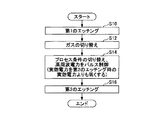
[プラズマエッチング方法]
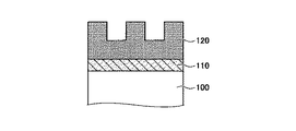
次に、本実施形態に係るプラズマエッチング方法について説明する。本実施形態に係るプラズマエッチング方法によりエッチングされる対象膜の一例を図2に示す。本実施形態では、エッチング対象膜は、下地膜100上にシリコン含有反射防止膜110(Siarc)、カーボンハードマスク120(CHM:Carbon Hard Mask)が積層された構成を有する。ただし、本実施形態に係るプラズマエッチング方法が適用されるエッチング対象膜に限定はなく、有機膜、酸化膜、窒化膜等のいずれの膜であってもよい。
[Plasma etching method]
Next, the plasma etching method according to the present embodiment will be described. An example of the target film etched by the plasma etching method according to the present embodiment is shown in FIG. In the present embodiment, the etching target film has a structure in which a silicon-containing antireflection film 110 (Siarc) and a carbon hard mask 120 (CHM: Carbon Hard Mask) are stacked on the
また、第1のエッチング工程が行われる第1のプロセス条件及び第2のエッチング工程が行われる第2のプロセス条件の一例を以下に示す。ただし、本実施形態に係るプラズマエッチング方法が適用される第1及び第2のプロセス条件のガス種に限定はなく、いずれの種類のガスであってもよい。また、本実施形態に係るプラズマエッチング方法が適用される第1及び第2のプロセス条件の高周波電力に限定はなく、連続波であってもよいし、パルス波であってもよい。なお、切替工程において供給される高周波電力はパルス波に限定される。
(第1のエッチング工程(CHMエッチング)における第1のプロセス条件)
ガス種 N2/H2
高周波電力 連続波 500W
(第2のエッチング工程(Siarcエッチング)における第2のプロセス条件)
ガス種 CF4
高周波電力 パルス波 500W(10kHz) デューティー比 30%
(切替工程における高周波電力)
高周波電力 パルス波 200W(10kHz) デューティー比 50%
(コンティニュアスプラズマを使用したエッチング)
以上のプロセス条件に基づき、図3に示したコンティニュアスプラズマを使用したプラズマエッチング方法が開始されると、制御装置50は、レシピに従い第1のプロセス条件に基づき第1のエッチング工程を実行する(ステップS10:第1のエッチング工程)。これにより、第1のエッチング工程にてカーボンハードマスク120がプラズマエッチングされる。
An example of the first process condition in which the first etching step is performed and the second process condition in which the second etching step is performed will be described below. However, there is no limitation on the gas types of the first and second process conditions to which the plasma etching method according to the present embodiment is applied, and any type of gas may be used. Moreover, there is no limitation in the high frequency electric power of the 1st and 2nd process conditions to which the plasma etching method concerning this embodiment is applied, A continuous wave may be sufficient and a pulse wave may be sufficient. In addition, the high frequency electric power supplied in a switching process is limited to a pulse wave.
(First process condition in the first etching step (CHM etching))
Gas type N 2 / H 2
High frequency power
(Second Process Condition in Second Etching Step (Siarc Etching))
Gas type CF 4
High frequency
(High-frequency power in the switching process)
High-frequency
(Etching using continuous plasma)
When the plasma etching method using the continuous plasma shown in FIG. 3 is started based on the above process conditions, the
次に、制御装置50は、レシピに従い、第1のプロセス条件のガスから第2のプロセス条件のガスに切り替える(ステップS12:ガスの切り替え)。これにより、チャンバCに供給されるガスが、N2ガスとH2ガスとの混合ガスからCF4ガスに切り替えられる。
Next, the
次に、制御装置50は、プロセスの切り替えを実行する(ステップS14:切替工程)。切替工程では、ガスを除くプロセス条件が、第1のプロセス条件から第2のプロセス条件へ切り替えられる。また、切替工程では、高周波電力が間欠的、すなわちパルス状に印加される。その際、制御装置50は、切替工程における実効電力を第2のエッチング工程における実効電力よりも低く制御する。
Next, the
実効電力は、高周波電力とデューティー比との乗算により算出される。よって、本実施形態では、切替工程における実効電力は、100W(=200W×0.5)となり、第2のエッチング工程時の実効電力150W(=500W×0.3)よりも低く制御されている。 The effective power is calculated by multiplying the high frequency power and the duty ratio. Therefore, in this embodiment, the effective power in the switching process is 100 W (= 200 W × 0.5), and is controlled to be lower than the effective power 150 W (= 500 W × 0.3) in the second etching process. .
次に、制御装置50は、レシピに従い第2のプロセス条件に基づき第2のエッチング工程を実行する(ステップS16:第2のエッチング工程)。これにより、第2のエッチング工程にてシリコン含有反射防止膜110がプラズマエッチングされる。
Next, the
上記に説明した本実施形態にかかるプラズマエッチング処理を実行した結果の一例を図4に示す。図4の左側に示す比較例では、コンティニュアスプラズマを使用したエッチングにおいて、第1のエッチング工程では連続波の高周波→切替工程では連続波の高周波→第2のエッチング工程ではパルス波の高周波が印加されている。 An example of the result of executing the plasma etching process according to the present embodiment described above is shown in FIG. In the comparative example shown on the left side of FIG. 4, in the etching using continuous plasma, the high frequency of the continuous wave in the first etching step → the high frequency of the continuous wave in the switching step → the high frequency of the pulse wave in the second etching step. Applied.
これに対して、図4の右側に示す本実施形態の一例では、コンティニュアスプラズマを使用したエッチングにおいて、第1のエッチング工程では連続波の高周波→切替工程ではパルス波の高周波→第2のエッチング工程ではパルス波の高周波が印加されている。また、比較例及び本実施形態ともに、切替工程における実効電力は100Wである。 On the other hand, in the example of this embodiment shown on the right side of FIG. 4, in the etching using continuous plasma, the high frequency of the continuous wave in the first etching step → the high frequency of the pulse wave in the switching step → the second In the etching process, a high frequency pulse wave is applied. In both the comparative example and the present embodiment, the effective power in the switching process is 100 W.
図4の結果によれば、比較例の場合、切替工程から第2のエッチング工程に遷移する際の高周波の反射量(RF Reflect)は30Wである。これに対して、本実施形態の場合、切替工程から第2のエッチング工程に遷移する際の高周波の反射量は15Wと半減している。 According to the result of FIG. 4, in the case of the comparative example, the amount of high-frequency reflection (RF Reflect) at the time of transition from the switching process to the second etching process is 30 W. On the other hand, in the case of the present embodiment, the amount of high-frequency reflection at the time of transition from the switching process to the second etching process is halved to 15 W.
図4の比較例の可変コンデンサC1、C2を見ると、プラズマの放電条件が変化したことに応じて高周波電源31の出力インピーダンスとプラズマ側の負荷インピーダンスとを一致させるための可変コンデンサC1、C2の整合位置の変動量が大きい。これに対して、図4の本実施形態の可変コンデンサC1、C2を見ると、可変コンデンサC1、C2の整合位置の変動量が比較例の場合よりも小さい。このため、本実施形態の場合、可変コンデンサC1、C2のトリマの位置を整合位置に合わせるまでの時間が比較例の場合よりも短くなる。この結果、本実施形態では、高周波の反射量が比較例の場合よりも小さくなると考えられる。
Looking at the variable capacitors C1 and C2 of the comparative example of FIG. 4, the variable capacitors C1 and C2 for matching the output impedance of the high
以上の結果から、パルス波の高周波電力を印加する場合、実効電力が同じ連続波の高周波電力を印加する場合よりも可変コンデンサC1、C1の移動量が減ることがわかる。その理由の一つとしては、整合器30では、パルスがオンのときの高周波電力に基づき上記のインピーダンス整合が行われるため、パルスがオンのときの高周波電力を上げる程可変コンデンサC1、C1の移動量は減る。この結果、可変コンデンサC1、C2のトリマの位置を整合位置に合わせるまでの時間が短くなり、高周波の反射量が減少すると考えられる。高周波の反射量が減少すると、プラズマの安定性が向上し、ウェハWのプラズマエッチング処理を均一に行うことができる。この結果、ウェハWの加工精度が向上し、歩留まりを高めることができる。
From the above results, it can be seen that when the high frequency power of the pulse wave is applied, the moving amounts of the variable capacitors C1 and C1 are smaller than when the continuous wave high frequency power having the same effective power is applied. One reason for this is that the
高周波の反射波を低減するために、切替工程において、例えば100W程度の低い高周波電力の連続波を印加することも考えられる。しかし、このような低電力の高周波を使用して切替工程を行うと、プラズマがチャンバCの内部に拡散され難い。この結果、低い電力の連続波の高周波を印加した場合には、エッチングの均一性が悪くなる。 In order to reduce high-frequency reflected waves, it is also conceivable to apply a continuous wave with high-frequency power as low as about 100 W in the switching step. However, when the switching process is performed using such a low power high frequency, the plasma is difficult to diffuse into the chamber C. As a result, when a high-frequency electric wave having a low power is applied, the etching uniformity deteriorates.
これに対して、本実施形態にかかるプラズマエッチング方法では、切替工程にて高周波電力のパルス波を使う。これにより、連続波の高周波と同じ実効電力であっても、パルスがオンしているときのパワーを高くできるため、プラズマがチャンバC内に広がり、ウェハWに均一にエッチング処理を行うことが可能となり、その結果、ウェハWの加工精度が向上する。 In contrast, in the plasma etching method according to the present embodiment, a pulse wave of high frequency power is used in the switching step. As a result, even when the effective power is the same as the high frequency of the continuous wave, the power when the pulse is on can be increased, so that the plasma spreads in the chamber C and the wafer W can be uniformly etched. As a result, the processing accuracy of the wafer W is improved.
例えば、電力が200Wの連続波の高周波と、周波数が10kHz、電力が400W、デューティー比が50%のパルス波の高周波とは、200Wの同一実効電力を有する。しかしながら、パルス波の高周波を用いた方が反射波は抑えられる結果となる。 For example, a continuous wave high frequency with a power of 200 W and a pulse wave high frequency with a frequency of 10 kHz, power of 400 W, and a duty ratio of 50% have the same effective power of 200 W. However, the reflected wave can be suppressed by using the high frequency of the pulse wave.
以上、切替工程においてパルス波の高周波電力を印加することで、切替工程から第2のエッチング工程に遷移する際に発生する高周波の反射量を小さくできることの説明を行った。これに加えて、本実施形態の効果としては、第1のエッチング工程から切替工程に遷移する際に発生する高周波の反射量も小さくできる。 As described above, it has been explained that the amount of high-frequency reflection generated when the switching process is changed to the second etching process can be reduced by applying high-frequency power of a pulse wave in the switching process. In addition to this, as an effect of the present embodiment, the amount of high-frequency reflection that occurs when transitioning from the first etching step to the switching step can also be reduced.
また、図4の高周波の電圧振幅Vppを参照すると、本実施形態の場合、比較例の場合に比べて実効電力が同じであっても電圧振幅Vppは高く維持されている。電圧振幅Vppが高い方がプラズマ維持に対して安定していること示すから、これによっても、切替工程においてパルス波の高周波電力を印加すると、プラズマの安定性が向上していることがわかる。 Further, referring to the high-frequency voltage amplitude Vpp of FIG. 4, in the case of the present embodiment, the voltage amplitude Vpp is maintained high even if the effective power is the same as in the case of the comparative example. Since the higher voltage amplitude Vpp is more stable with respect to the plasma maintenance, it can be seen that the stability of the plasma is improved by applying the high frequency power of the pulse wave in the switching step.
[プラズマエッチング方法(他の例)]
次に、上記第1及び第2のプロセスとは異なるプロセス条件において、本実施形態に係るプラズマエッチング方法を行った場合について、図5を参照しながら説明する。図5は、上記異なるプロセス条件において本実施形態に係るプラズマエッチング方法を行った場合の結果の一例を示す。
[Plasma etching method (other examples)]
Next, the case where the plasma etching method according to the present embodiment is performed under process conditions different from those of the first and second processes will be described with reference to FIG. FIG. 5 shows an example of a result when the plasma etching method according to the present embodiment is performed under the different process conditions.
この例では、第1のエッチング工程が行われる第1のプロセス条件、第2のエッチング工程が行われる第2のプロセス条件及び切替工程における高周波電力の条件は以下である。切替工程における高周波電力以外のプロセス条件は、切替工程の開始時に第1のプロセスから第2のプロセスに切り替えられる。
(第1のプロセス条件:CHMエッチング)
ガス種 N2/O2
高周波電力 連続波 1000W
(第2のプロセス条件:Siarcエッチング)
ガス種 NF3/N2
高周波電力 連続波 400W
(切替工程における高周波電力)
(a)連続波 100W
(b)連続波 300W
(c)連続波 400W
(d)パルス波 400W(10kHz) デューティー比 50%
上記のプロセス条件にてコンティニュアスプラズマを使用したエッチング処理を実行したところ、(a)及び(b)では高周波の反射量が大きく、(c)及び(d)では高周波の反射量が小さい結果となっている。(c)の切替工程のように第2のエッチング工程と同じ400Wの連続波の高周波電力を使うと高周波の反射が少ないことがわかる。
In this example, the first process condition in which the first etching process is performed, the second process condition in which the second etching process is performed, and the condition of the high-frequency power in the switching process are as follows. Process conditions other than high-frequency power in the switching step are switched from the first process to the second process at the start of the switching step.
(First process condition: CHM etching)
Gas type N 2 / O 2
High frequency power continuous wave 1000W
(Second process condition: Siarc etching)
Gas type NF 3 / N 2
High frequency power
(High-frequency power in the switching process)
(A)
(B)
(C)
(D)
When etching processing using continuous plasma was performed under the above process conditions, the results of (a) and (b) show that the amount of high-frequency reflection was large, and (c) and (d) show that the amount of high-frequency reflection was small. It has become. It can be seen that when the same 400 W continuous wave high frequency power as in the second etching step is used as in the switching step (c), the high frequency reflection is small.
しかし、400Wの連続波の高周波電力を使うと、切替工程においてエッチングが促進される。この結果、第1のエッチング工程のガスの影響を受けて想定外のエッチング処理が進行し、ウェハWの加工にバラツキが発生し易くなり、エッチングの均一性が低下する。 However, if 400 W continuous wave high frequency power is used, etching is accelerated in the switching step. As a result, an unexpected etching process proceeds under the influence of the gas in the first etching process, and the wafer W is likely to vary in processing, resulting in a decrease in etching uniformity.
そこで、切替工程においてエッチングを抑制するために、(b)の切替工程では高周波の電力値を300Wに下げ、(a)の切替工程では高周波の電力値を100Wに下げる。この結果、(b)の切替工程では51Wの高周波の反射が検知され、(a)の切替工程では38W〜65Wの高周波の反射が検知され、いずれの場合にもプラズマが不安定になっている。 Therefore, in order to suppress etching in the switching step, the high-frequency power value is reduced to 300 W in the switching step (b), and the high-frequency power value is reduced to 100 W in the switching step (a). As a result, the high frequency reflection of 51 W is detected in the switching step (b), and the high frequency reflection of 38 W to 65 W is detected in the switching step (a), and the plasma is unstable in any case. .
一方、(d)の切替工程では、デューティー比が50%のパルス波の高周波が供給される。この結果、(d)の切替工程では19Wの高周波の反射が検知され、プラズマが安定することがわかる。加えて、(d)の切替工程では実効電力が200Wであるため、(b)〜(c)の切替工程よりも切替工程におけるエッチングが抑制されることがわかる。 On the other hand, in the switching step (d), a high frequency pulse wave having a duty ratio of 50% is supplied. As a result, it can be seen that in the switching step (d), high-frequency reflection of 19 W is detected and the plasma is stabilized. In addition, since the effective power is 200 W in the switching step (d), it can be seen that etching in the switching step is suppressed more than in the switching steps (b) to (c).
具体的には、(d)の切替工程では実効電力が200Wであり、(b)の高周波の実効電力(300W)よりも小さいにもかかわらず高周波の反射量は低減されている。これは、パルス波の高周波を印加すると、実効電力が同一又は近似する連続波の高周波を印加するよりも、整合器30の可変コンデンサC1,C2の整合位置の移動量を小さくできることを示している。
Specifically, in the switching step (d), the effective power is 200 W, and the amount of high-frequency reflection is reduced in spite of being smaller than the high-frequency effective power (300 W) in (b). This indicates that when a high frequency pulse wave is applied, the amount of movement of the matching position of the variable capacitors C1 and C2 of the
[デューティー比の依存性]
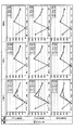
次に、切替工程で印加するパルス波の高周波のデューティー比の依存性について実験した結果について、図6および図7を参照しながら説明する。ここでは、図6の上段、中断、下段及び図7の上段、中断、下段に示されるすべての結果において、切替工程でパルス波の高周波が印加されることが条件とされる。また、印加される高周波の周波数は、左から0.5kHz、10kHz、20kHzである。その他の各プロセス条件は次の通りである。
・図6の上段
Siarcのエッチング
ガス種 CF4
高周波 パルス波 600W
・図6の中段
Siarcのエッチング
ガス種 CF4/O2
高周波 パルス波 800W
・図6の下段
CHMのエッチング
ガス種 N2/O2
高周波 パルス波 500W
・図7の上段
C(カーボン)を除くHM(ハードマスク)のエッチング
ガス種 CHF3/Ar/O2
高周波 パルス波 800W
・図7の中段
Ox(酸化膜)のエッチング
ガス種 C4F8/Ar/O2
高周波 パルス波 1000W
・図7の下段
SiN(窒化膜)におけるエッチング
ガス種 CHF3/Ar/O2/CF4
高周波 パルス波 800W
これによれば、0.5kHz、10kHz、20kHzのいずれの周波数の場合にも、デューティー比を最大で10%〜90%に変化させても、可変コンデンサC1、C2の位置は、ほぼ一致し、変化していないことがわかる。
[Duty ratio dependency]
Next, the results of experiments on the dependence of the high frequency duty ratio of the pulse wave applied in the switching step will be described with reference to FIGS. Here, in all the results shown in the upper part, interruption, lower part of FIG. 6 and the upper part, interruption, lower part of FIG. 7, it is a condition that the high frequency of the pulse wave is applied in the switching step. Moreover, the frequency of the applied high frequency is 0.5 kHz, 10 kHz, and 20 kHz from the left. Other process conditions are as follows.
-Etching gas type CF 4 in the upper Siarc in FIG.
High
-Etching gas type CF 4 / O 2 of middle stage Siarc in FIG.
High frequency pulse wave 800W
-Etching gas type of lower CHM in FIG. 6 N 2 / O 2
High
-Etching gas species of HM (hard mask) excluding upper stage C (carbon) in FIG. 7 CHF 3 / Ar / O 2
High frequency pulse wave 800W
Etching gas species the middle Ox in FIG. 7 (oxide film) C 4 F 8 / Ar / O 2
High frequency pulse wave 1000W
Etching gas type in lower SiN (nitride film) in FIG. 7 CHF 3 / Ar / O 2 / CF 4
High frequency pulse wave 800W
According to this, even when the duty ratio is changed from 10% to 90% at the maximum in any of the frequencies of 0.5 kHz, 10 kHz, and 20 kHz, the positions of the variable capacitors C1 and C2 are substantially the same. You can see that it has not changed.
例えば、パルス波の高周波の電力が400Wの場合であってデューティー比が10%の場合、実効電力は40Wであり、デューティー比が90%の場合、実効電力は360Wである。このように、実効電力に9倍の差があっても、可変コンデンサC1、C2の位置はほぼ一致している。これにより、本実施形態にかかるプラズマエッチング方法によれば、切替工程における高周波の実効電力を第2のエッチング工程における高周波の実効電力以下にすることで、高周波の反射を下げ、かつ切替工程におけるエッチングを抑制することができる。その際、本実施形態にかかるプラズマエッチング方法は、印加するパルス波の高周波のデューティー比に依存性しないことがわかる。 For example, when the high frequency power of the pulse wave is 400 W and the duty ratio is 10%, the effective power is 40 W, and when the duty ratio is 90%, the effective power is 360 W. Thus, even if there is a nine-fold difference in effective power, the positions of the variable capacitors C1 and C2 are almost the same. Thereby, according to the plasma etching method according to the present embodiment, the high-frequency effective power in the switching step is set to be equal to or lower than the high-frequency effective power in the second etching step, thereby reducing high-frequency reflection and etching in the switching step. Can be suppressed. At that time, it can be seen that the plasma etching method according to the present embodiment does not depend on the high-frequency duty ratio of the applied pulse wave.
また、図6の上段、中断、下段及び図7の上段、中断、下段の結果を得るために使用したガス種はすべて異なっている。よって、本実施形態にかかるプラズマエッチング方法は、ガス種に依存性しないことがわかる。 Also, the gas types used to obtain the results of the upper, interrupted, and lower stages of FIG. 6 and the upper, interrupted, and lower stages of FIG. 7 are all different. Therefore, it can be seen that the plasma etching method according to the present embodiment does not depend on the gas type.
[周波数の依存性]
最後に、周波数の依存性について実験した結果について、図8を参照しながら説明する。図8の上段、中断、下段に示されるすべての結果において、切替工程ではパルス波の高周波が印加される。また、デューティー比は、左から10%、50%、90%である。各プロセス条件は次の通りである。
・図8の上段
Siarcのエッチング
ガス種 CF4
高周波 パルス波 600W
・図8の中段
Siarcのエッチング
ガス種 CF4/O2
高周波 パルス波 800W
・図8の下段
CHMのエッチング
ガス種 N2/O2
高周波 パルス波 500W
これによれば、0.5kHz、10kHz、20kHzのいずれの周波数の場合にも、デューティー比を10%〜90%に変化させても、可変コンデンサC1、C2の位置は、ほぼ一致し、変化していないことが示されている。以上から、本実施形態にかかるプラズマエッチング方法は、パルス波の高周波の周波数に依存性しないことがわかる。
[Dependency on frequency]
Finally, the results of experiments on frequency dependence will be described with reference to FIG. In all the results shown in the upper part, interruption, and lower part of FIG. 8, a high frequency pulse wave is applied in the switching step. The duty ratio is 10%, 50%, and 90% from the left. Each process condition is as follows.
-Etching gas type CF 4 in the upper Siarc in FIG.
High
-Etching gas type CF 4 / O 2 of middle stage Siarc in FIG.
High frequency pulse wave 800W
-Etching gas type of lower CHM in FIG. 8 N 2 / O 2
High
According to this, in any frequency of 0.5 kHz, 10 kHz, and 20 kHz, even if the duty ratio is changed from 10% to 90%, the positions of the variable capacitors C1, C2 are almost the same and change. It has not been shown. From the above, it can be seen that the plasma etching method according to the present embodiment does not depend on the high frequency of the pulse wave.
以上に説明したように、本実施形態にかかるプラズマエッチング方法によれば、切替工程におけるパルス波の高周波の実効電力を第2のエッチング工程における実効電力以下にすることで高周波の反射波を低減することができ、プラズマを安定させることができる。また、切替工程においてエッチングを抑制させることができる。 As described above, according to the plasma etching method according to the present embodiment, the high-frequency reflected wave is reduced by setting the high-frequency effective power of the pulse wave in the switching step to be equal to or lower than the effective power in the second etching step. And the plasma can be stabilized. Moreover, etching can be suppressed in the switching step.
以上、プラズマエッチング方法を上記実施形態により説明したが、本発明にかかるプラズマエッチング方法は上記実施形態に限定されるものではなく、本発明の範囲内で種々の変形及び改良が可能である。上記複数の実施形態に記載された事項は、矛盾しない範囲で組み合わせることができる。 As described above, the plasma etching method has been described in the above embodiment. However, the plasma etching method according to the present invention is not limited to the above embodiment, and various modifications and improvements can be made within the scope of the present invention. The matters described in the above embodiments can be combined within a consistent range.
例えば、本発明に係るプラズマエッチング方法は、容量結合型プラズマ(CCP:Capacitively Coupled Plasma)装置、誘導結合型プラズマ(ICP:Inductively Coupled Plasma)、ラジアルラインスロットアンテナを用いたCVD(Chemical Vapor Deposition)装置、ヘリコン波励起型プラズマ(HWP:Helicon Wave Plasma)装置、電子サイクロトロン共鳴プラズマ(ECR:Electron Cyclotron Resonance Plasma)装置等において使用可能である。 For example, a plasma etching method according to the present invention includes a capacitively coupled plasma (CCP) apparatus, an inductively coupled plasma (ICP) apparatus, and a CVD (Chemical Vapor Deposition) apparatus using a radial line slot antenna. It can be used in a Helicon Wave Plasma (HWP) device, an Electron Cyclotron Resonance Plasma (ECR) device, and the like.
また、本発明にかかるプラズマ処理装置により処理される基板は、ウェハに限られず、例えば、フラットパネルディスプレイ(Flat Panel Display)用の大型基板、EL素子又は太陽電池用の基板であってもよい。 The substrate processed by the plasma processing apparatus according to the present invention is not limited to a wafer, and may be, for example, a large substrate for a flat panel display, a substrate for an EL element, or a solar cell.
1:プラズマ処理装置
10:ガス供給源
21:載置台
30:整合器
40:排気装置
50:制御装置
C:チャンバ
C1,C2:可変コンデンサ
L:インダクタ
1: Plasma processing apparatus 10: Gas supply source 21: Mounting table 30: Matching device 40: Exhaust device 50: Control device C: Chamber C1, C2: Variable capacitor L: Inductor
Claims (3)
第1のプロセス条件に基づき、第1の実効電力を有する第1の高周波電力を供給しながら第1のプラズマエッチングを行う第1のエッチング工程と、
第1のプロセス条件と異なる第2のプロセス条件に基づき、第2の実効電力を有する第2の高周波電力を供給しながら第2のプラズマエッチングを行う第2のエッチング工程と、
前記第1及び第2のエッチング工程の間において、第3の実効電力を有する第3の高周波電力を間欠的に供給する切替工程と、を有し、
前記切替工程の開始前に、ガスのプロセス条件を前記第1のプロセス条件から前記第2のプロセス条件に切り替え、
前記切替工程における第3の高周波の実効電力は、前記第1のエッチング工程における前記第1の高周波電力の前記第1の実効電力及び前記第2のエッチング工程における前記第2の高周波電力の前記第2の実効電力以下であり、前記第3の高周波電力は、前記第3の高周波電力を間欠的に供給している間、一定のデューティー比を有するプラズマエッチング方法。 A plasma etching method for performing desired etching by switching process conditions while supplying high-frequency power and maintaining plasma,
A first etching step for performing a first plasma etching based on a first process condition while supplying a first high-frequency power having a first effective power;
A second etching step of performing a second plasma etching while supplying a second high-frequency power having a second effective power based on a second process condition different from the first process condition;
A switching step of intermittently supplying a third high-frequency power having a third effective power between the first and second etching steps,
Before starting the switching step, the gas process condition is switched from the first process condition to the second process condition,
The third high-frequency effective power in the switching step is the first effective power of the first high-frequency power in the first etching step and the second high-frequency power in the second etching step. 2. The plasma etching method according to claim 1, wherein the third high-frequency power has a constant duty ratio while the third high-frequency power is intermittently supplied.
請求項1に記載のプラズマエッチング方法。 In response to the start of the switching step, process conditions other than the third high-frequency power are switched from the first process condition to the second process condition.
The plasma etching method according to claim 1.
第1のプロセス条件に基づき、連続波である第1の高周波電力を供給しながら第1のプラズマエッチングを行う第1のエッチング工程と、
第1のプロセス条件と異なる第2のプロセス条件に基づき、第2の実効電力を有する第2の高周波電力を供給しながら第2のプラズマエッチングを行う第2のエッチング工程と、
前記第1及び第2のエッチング工程の間において、第3の実効電力を有する第3の高周波電力を間欠的に供給する切替工程と、を有し、
前記切替工程の開始前に、ガスのプロセス条件を前記第1のプロセス条件から前記第2のプロセス条件に切り替え、
前記切替工程における第3の高周波の実効電力は、前記第2のエッチング工程における前記第2の高周波電力の前記第2の実効電力以下であり、前記第3の高周波電力は、前記第3の高周波電力を間欠的に供給している間、一定のデューティー比を有するプラズマエッチング方法。 A plasma etching method for performing desired etching by switching process conditions while supplying high-frequency power and maintaining plasma,
A first etching step of performing a first plasma etching based on a first process condition while supplying a first high-frequency power that is a continuous wave;
A second etching step of performing a second plasma etching while supplying a second high-frequency power having a second effective power based on a second process condition different from the first process condition;
A switching step of intermittently supplying a third high-frequency power having a third effective power between the first and second etching steps,
Before starting the switching step, the gas process condition is switched from the first process condition to the second process condition,
A third high-frequency effective power in the switching step is equal to or lower than the second effective power of the second high-frequency power in the second etching step, and the third high-frequency power is the third high-frequency power. A plasma etching method having a constant duty ratio while power is intermittently supplied.
Priority Applications (4)
| Application Number | Priority Date | Filing Date | Title |
|---|---|---|---|
| JP2014246069A JP6316735B2 (en) | 2014-12-04 | 2014-12-04 | Plasma etching method |
| KR1020150166149A KR101900136B1 (en) | 2014-12-04 | 2015-11-26 | Plasma etching method |
| TW104140258A TWI613721B (en) | 2014-12-04 | 2015-12-02 | Plasma etching method |
| US14/956,719 US9779962B2 (en) | 2014-12-04 | 2015-12-02 | Plasma etching method |
Applications Claiming Priority (1)
| Application Number | Priority Date | Filing Date | Title |
|---|---|---|---|
| JP2014246069A JP6316735B2 (en) | 2014-12-04 | 2014-12-04 | Plasma etching method |
Publications (3)
| Publication Number | Publication Date |
|---|---|
| JP2016111140A JP2016111140A (en) | 2016-06-20 |
| JP2016111140A5 JP2016111140A5 (en) | 2017-10-26 |
| JP6316735B2 true JP6316735B2 (en) | 2018-04-25 |
Family
ID=56094952
Family Applications (1)
| Application Number | Title | Priority Date | Filing Date |
|---|---|---|---|
| JP2014246069A Active JP6316735B2 (en) | 2014-12-04 | 2014-12-04 | Plasma etching method |
Country Status (4)
| Country | Link |
|---|---|
| US (1) | US9779962B2 (en) |
| JP (1) | JP6316735B2 (en) |
| KR (1) | KR101900136B1 (en) |
| TW (1) | TWI613721B (en) |
Families Citing this family (2)
| Publication number | Priority date | Publication date | Assignee | Title |
|---|---|---|---|---|
| CN106415779B (en) * | 2013-12-17 | 2020-01-21 | 东京毅力科创株式会社 | System and method for controlling plasma density |
| JP6541596B2 (en) * | 2016-03-22 | 2019-07-10 | 東京エレクトロン株式会社 | Plasma treatment method |
Family Cites Families (28)
| Publication number | Priority date | Publication date | Assignee | Title |
|---|---|---|---|---|
| KR890004881B1 (en) * | 1983-10-19 | 1989-11-30 | 가부시기가이샤 히다찌세이사꾸쇼 | Plasma treating method and device thereof |
| JPH0514435A (en) | 1991-07-08 | 1993-01-22 | Fujitsu Ltd | In-equipment monitor system |
| JP2000012529A (en) * | 1998-06-26 | 2000-01-14 | Hitachi Ltd | Surface machining apparatus |
| CN100462475C (en) * | 2001-08-29 | 2009-02-18 | 东京电子株式会社 | Apparatus and method for plasma processing |
| US6700090B2 (en) * | 2002-04-26 | 2004-03-02 | Hitachi High-Technologies Corporation | Plasma processing method and plasma processing apparatus |
| JP3681718B2 (en) * | 2002-08-12 | 2005-08-10 | 株式会社日立ハイテクノロジーズ | Plasma processing apparatus and method |
| US7025895B2 (en) * | 2002-08-15 | 2006-04-11 | Hitachi High-Technologies Corporation | Plasma processing apparatus and method |
| US20070066038A1 (en) | 2004-04-30 | 2007-03-22 | Lam Research Corporation | Fast gas switching plasma processing apparatus |
| JP5192209B2 (en) * | 2006-10-06 | 2013-05-08 | 東京エレクトロン株式会社 | Plasma etching apparatus, plasma etching method, and computer-readable storage medium |
| JP5094289B2 (en) * | 2007-09-05 | 2012-12-12 | 株式会社日立ハイテクノロジーズ | Plasma processing equipment |
| JP5008509B2 (en) | 2007-09-25 | 2012-08-22 | パナソニック株式会社 | Plasma processing method |
| JP5367689B2 (en) * | 2008-03-07 | 2013-12-11 | 株式会社アルバック | Plasma processing method |
| KR101489326B1 (en) * | 2008-09-09 | 2015-02-11 | 삼성전자주식회사 | Method of processing a substrate |
| CN102474971B (en) * | 2009-08-07 | 2015-03-04 | 株式会社京三制作所 | Pulse modulated RF power control method and pulse modulated RF power supply device |
| JP5461148B2 (en) * | 2009-11-05 | 2014-04-02 | 株式会社日立ハイテクノロジーズ | Plasma etching method and apparatus |
| US8709953B2 (en) * | 2011-10-27 | 2014-04-29 | Applied Materials, Inc. | Pulsed plasma with low wafer temperature for ultra thin layer etches |
| US20130119018A1 (en) * | 2011-11-15 | 2013-05-16 | Keren Jacobs Kanarik | Hybrid pulsing plasma processing systems |
| US8808561B2 (en) * | 2011-11-15 | 2014-08-19 | Lam Research Coporation | Inert-dominant pulsing in plasma processing systems |
| JP5977509B2 (en) * | 2011-12-09 | 2016-08-24 | 東京エレクトロン株式会社 | Plasma processing method and plasma processing apparatus |
| US8883028B2 (en) * | 2011-12-28 | 2014-11-11 | Lam Research Corporation | Mixed mode pulsing etching in plasma processing systems |
| JP5887201B2 (en) * | 2012-05-14 | 2016-03-16 | 東京エレクトロン株式会社 | Substrate processing method, substrate processing apparatus, substrate processing program, and storage medium |
| JP5822795B2 (en) * | 2012-07-17 | 2015-11-24 | 株式会社日立ハイテクノロジーズ | Plasma processing equipment |
| JP6035606B2 (en) | 2013-04-09 | 2016-11-30 | 株式会社日立ハイテクノロジーズ | Plasma processing method and plasma processing apparatus |
| JP2015099824A (en) * | 2013-11-18 | 2015-05-28 | 株式会社東芝 | Substrate processing device and control method |
| US9620382B2 (en) * | 2013-12-06 | 2017-04-11 | University Of Maryland, College Park | Reactor for plasma-based atomic layer etching of materials |
| JP6424024B2 (en) * | 2014-06-24 | 2018-11-14 | 株式会社日立ハイテクノロジーズ | Plasma processing apparatus and plasma processing method |
| US9768033B2 (en) * | 2014-07-10 | 2017-09-19 | Tokyo Electron Limited | Methods for high precision etching of substrates |
| KR102247560B1 (en) * | 2014-07-14 | 2021-05-03 | 삼성전자 주식회사 | Plasma generating method in RPS(Remote Plasma Source) and method for fabricating semiconductor device comprising the same plasma generating method |
-
2014
- 2014-12-04 JP JP2014246069A patent/JP6316735B2/en active Active
-
2015
- 2015-11-26 KR KR1020150166149A patent/KR101900136B1/en active IP Right Grant
- 2015-12-02 TW TW104140258A patent/TWI613721B/en active
- 2015-12-02 US US14/956,719 patent/US9779962B2/en active Active
Also Published As
| Publication number | Publication date |
|---|---|
| TWI613721B (en) | 2018-02-01 |
| JP2016111140A (en) | 2016-06-20 |
| TW201631657A (en) | 2016-09-01 |
| KR101900136B1 (en) | 2018-09-18 |
| US20160163554A1 (en) | 2016-06-09 |
| KR20160067740A (en) | 2016-06-14 |
| US9779962B2 (en) | 2017-10-03 |
Similar Documents
| Publication | Publication Date | Title |
|---|---|---|
| TWI586224B (en) | Apparatus for tuning a system operating a plasma process | |
| CN110246760B (en) | Etching method | |
| KR102031388B1 (en) | Triode reactor design with multiple radiofrequency powers | |
| JP2016143890A (en) | Method for increasing pattern density by self-aligned patterning integration scheme | |
| JP2016143890A5 (en) | ||
| TWI633599B (en) | Etching method and etching device | |
| KR20100028486A (en) | Plasma processing method and resist pattern modifying method | |
| US10903051B2 (en) | Matching method and plasma processing apparatus | |
| KR102304163B1 (en) | Etching method | |
| JP6316735B2 (en) | Plasma etching method | |
| TW202147925A (en) | Plasma processing apparatus and plasma processing | |
| US10964511B2 (en) | Semiconductor manufacturing device and method of operating the same | |
| KR20210020808A (en) | Substrate processing method, pressure control apparatus and substrate processing system | |
| JP2001257198A (en) | Plasma processing method | |
| JP7313293B2 (en) | Processing method and plasma processing apparatus | |
| US20230120474A1 (en) | Plasma etching apparatus and method for operating the same | |
| US20230420223A1 (en) | Plasma Processing Method and Plasma Processing Apparatus | |
| WO2023210399A1 (en) | Plasma treatment device, power source system, and plasma treatment method | |
| KR20230085168A (en) | Substrate processing method and substrate processing apparatus | |
| TW202201525A (en) | Substrate processing method and substrate processing apparatus | |
| KR20200116055A (en) | Plasma etching apparatus and plasma etching method | |
| WO2023096729A1 (en) | Ion energy control on electrodes in a plasma reactor | |
| KR101813321B1 (en) | Plasma etching method and plasma etching apparatus | |
| CN115513024A (en) | ICP etching device and using method thereof | |
| KR20240016726A (en) | Capacitively coupled plasma generator and inductively coupled plasma generator for increasing plasma generation efficiency |
Legal Events
| Date | Code | Title | Description |
|---|---|---|---|
| A521 | Request for written amendment filed |
Free format text: JAPANESE INTERMEDIATE CODE: A523 Effective date: 20170908 |
|
| A621 | Written request for application examination |
Free format text: JAPANESE INTERMEDIATE CODE: A621 Effective date: 20170908 |
|
| A871 | Explanation of circumstances concerning accelerated examination |
Free format text: JAPANESE INTERMEDIATE CODE: A871 Effective date: 20170908 |
|
| A977 | Report on retrieval |
Free format text: JAPANESE INTERMEDIATE CODE: A971007 Effective date: 20171218 |
|
| A975 | Report on accelerated examination |
Free format text: JAPANESE INTERMEDIATE CODE: A971005 Effective date: 20171221 |
|
| A131 | Notification of reasons for refusal |
Free format text: JAPANESE INTERMEDIATE CODE: A131 Effective date: 20180109 |
|
| A521 | Request for written amendment filed |
Free format text: JAPANESE INTERMEDIATE CODE: A523 Effective date: 20180226 |
|
| TRDD | Decision of grant or rejection written | ||
| A01 | Written decision to grant a patent or to grant a registration (utility model) |
Free format text: JAPANESE INTERMEDIATE CODE: A01 Effective date: 20180313 |
|
| A61 | First payment of annual fees (during grant procedure) |
Free format text: JAPANESE INTERMEDIATE CODE: A61 Effective date: 20180328 |
|
| R150 | Certificate of patent or registration of utility model |
Ref document number: 6316735 Country of ref document: JP Free format text: JAPANESE INTERMEDIATE CODE: R150 |
|
| R250 | Receipt of annual fees |
Free format text: JAPANESE INTERMEDIATE CODE: R250 |
|
| R250 | Receipt of annual fees |
Free format text: JAPANESE INTERMEDIATE CODE: R250 |
|
| R250 | Receipt of annual fees |
Free format text: JAPANESE INTERMEDIATE CODE: R250 |
|
| R250 | Receipt of annual fees |
Free format text: JAPANESE INTERMEDIATE CODE: R250 |