JP5367689B2 - Plasma processing method - Google Patents
Plasma processing method Download PDFInfo
- Publication number
- JP5367689B2 JP5367689B2 JP2010501961A JP2010501961A JP5367689B2 JP 5367689 B2 JP5367689 B2 JP 5367689B2 JP 2010501961 A JP2010501961 A JP 2010501961A JP 2010501961 A JP2010501961 A JP 2010501961A JP 5367689 B2 JP5367689 B2 JP 5367689B2
- Authority
- JP
- Japan
- Prior art keywords
- etching
- plasma processing
- plasma
- substrate
- processing method
- Prior art date
- Legal status (The legal status is an assumption and is not a legal conclusion. Google has not performed a legal analysis and makes no representation as to the accuracy of the status listed.)
- Active
Links
Images


Classifications
-
- H—ELECTRICITY
- H01—ELECTRIC ELEMENTS
- H01J—ELECTRIC DISCHARGE TUBES OR DISCHARGE LAMPS
- H01J37/00—Discharge tubes with provision for introducing objects or material to be exposed to the discharge, e.g. for the purpose of examination or processing thereof
- H01J37/32—Gas-filled discharge tubes
- H01J37/34—Gas-filled discharge tubes operating with cathodic sputtering
-
- H—ELECTRICITY
- H01—ELECTRIC ELEMENTS
- H01J—ELECTRIC DISCHARGE TUBES OR DISCHARGE LAMPS
- H01J37/00—Discharge tubes with provision for introducing objects or material to be exposed to the discharge, e.g. for the purpose of examination or processing thereof
- H01J37/32—Gas-filled discharge tubes
- H01J37/32009—Arrangements for generation of plasma specially adapted for examination or treatment of objects, e.g. plasma sources
- H01J37/32082—Radio frequency generated discharge
- H01J37/321—Radio frequency generated discharge the radio frequency energy being inductively coupled to the plasma
-
- H—ELECTRICITY
- H01—ELECTRIC ELEMENTS
- H01J—ELECTRIC DISCHARGE TUBES OR DISCHARGE LAMPS
- H01J37/00—Discharge tubes with provision for introducing objects or material to be exposed to the discharge, e.g. for the purpose of examination or processing thereof
- H01J37/32—Gas-filled discharge tubes
- H01J37/32009—Arrangements for generation of plasma specially adapted for examination or treatment of objects, e.g. plasma sources
- H01J37/32082—Radio frequency generated discharge
- H01J37/32137—Radio frequency generated discharge controlling of the discharge by modulation of energy
- H01J37/32146—Amplitude modulation, includes pulsing
-
- H—ELECTRICITY
- H01—ELECTRIC ELEMENTS
- H01J—ELECTRIC DISCHARGE TUBES OR DISCHARGE LAMPS
- H01J37/00—Discharge tubes with provision for introducing objects or material to be exposed to the discharge, e.g. for the purpose of examination or processing thereof
- H01J37/32—Gas-filled discharge tubes
- H01J37/32431—Constructional details of the reactor
- H01J37/3244—Gas supply means
- H01J37/32449—Gas control, e.g. control of the gas flow
-
- H—ELECTRICITY
- H01—ELECTRIC ELEMENTS
- H01L—SEMICONDUCTOR DEVICES NOT COVERED BY CLASS H10
- H01L21/00—Processes or apparatus adapted for the manufacture or treatment of semiconductor or solid state devices or of parts thereof
- H01L21/02—Manufacture or treatment of semiconductor devices or of parts thereof
- H01L21/04—Manufacture or treatment of semiconductor devices or of parts thereof the devices having at least one potential-jump barrier or surface barrier, e.g. PN junction, depletion layer or carrier concentration layer
- H01L21/18—Manufacture or treatment of semiconductor devices or of parts thereof the devices having at least one potential-jump barrier or surface barrier, e.g. PN junction, depletion layer or carrier concentration layer the devices having semiconductor bodies comprising elements of Group IV of the Periodic System or AIIIBV compounds with or without impurities, e.g. doping materials
- H01L21/30—Treatment of semiconductor bodies using processes or apparatus not provided for in groups H01L21/20 - H01L21/26
- H01L21/302—Treatment of semiconductor bodies using processes or apparatus not provided for in groups H01L21/20 - H01L21/26 to change their surface-physical characteristics or shape, e.g. etching, polishing, cutting
- H01L21/306—Chemical or electrical treatment, e.g. electrolytic etching
- H01L21/3065—Plasma etching; Reactive-ion etching
- H01L21/30655—Plasma etching; Reactive-ion etching comprising alternated and repeated etching and passivation steps, e.g. Bosch process
-
- H—ELECTRICITY
- H01—ELECTRIC ELEMENTS
- H01J—ELECTRIC DISCHARGE TUBES OR DISCHARGE LAMPS
- H01J2237/00—Discharge tubes exposing object to beam, e.g. for analysis treatment, etching, imaging
- H01J2237/32—Processing objects by plasma generation
- H01J2237/33—Processing objects by plasma generation characterised by the type of processing
- H01J2237/334—Etching
Description
本発明は、シリコン基板の表面に高アスペクト比の孔やディープトレンチを形成するためのプラズマ処理方法に関し、更に詳しくは、エッチング開始から終了にわたって均一な面内分布を維持することができるプラズマ処理方法に関する。 The present invention relates to a plasma processing method for forming high aspect ratio holes and deep trenches on the surface of a silicon substrate, and more particularly, a plasma processing method capable of maintaining a uniform in-plane distribution from the start to the end of etching. About.
従来、シリコン基板の表面の加工には、プラズマエッチング(ドライエッチング)方法が広く用いられている。室温における原子状(ラジカル)フッ素とシリコンの反応は自発的であり、比較的高いエッチングレートが得られることから、シリコン基板のエッチングでは、エッチングガスとしてSF6、NF3、COF2、XeF2等のフッ素を含むガスが多用されている。Conventionally, a plasma etching (dry etching) method has been widely used for processing a surface of a silicon substrate. The reaction between atomic (radical) fluorine and silicon at room temperature is spontaneous, and a relatively high etching rate is obtained. Therefore, in etching a silicon substrate, SF 6 , NF 3 , COF 2 , XeF 2, etc. are used as etching gases. Gases containing fluorine are frequently used.
一方、フッ素を含むエッチングガスを用いたシリコン基板のドライエッチングは等方的であるため、形成されたエッチングパターン(凹部)の側壁部にもエッチングが進行する。このため、スルーホールやディープトレンチなどの微細でアスペクト比の高いビアを高精度に形成することが困難であった。 On the other hand, since dry etching of a silicon substrate using an etching gas containing fluorine is isotropic, etching also proceeds to the side wall portion of the formed etching pattern (concave portion). For this reason, it has been difficult to form fine and high aspect ratio vias such as through holes and deep trenches with high accuracy.
そこで近年、エッチングパターンの側壁部に保護膜を形成しながら基板をエッチングすることで、エッチングの横方向の広がりを抑え、パターン側壁部の垂直性を維持できるシリコン基板の深掘り加工技術が提案されている。 Therefore, in recent years, silicon substrate deep digging technology has been proposed that can suppress the lateral spread of the etching and maintain the verticality of the pattern side wall by etching the substrate while forming a protective film on the side wall of the etching pattern. ing.
例えば特許文献1には、エッチング工程と保護膜形成工程を交互に繰り返すことで、エッチングパターンの側壁部にポリマー層からなる保護膜を形成しながらエッチングする方法が開示されている。特に、保護膜の成膜として、基板に対向配置されたターゲット材に対するアルゴンガスを用いたスパッタ法が開示されている。 For example, Patent Document 1 discloses a method of performing etching while forming a protective film made of a polymer layer on a sidewall portion of an etching pattern by alternately repeating an etching process and a protective film forming process. In particular, as a method for forming a protective film, a sputtering method using argon gas for a target material arranged to face a substrate is disclosed.
保護膜形成工程でエッチングパターンの側壁部に形成されたポリマー層は、エッチングパターンの底部に形成されたポリマー層に比べて、エッチング工程において除去される量が少ないため、このパターン側壁部に形成されたポリマー層が保護膜として機能し、エッチング方向をパターンの深さ方向に制限する異方性エッチングが実現可能となる。 The polymer layer formed on the sidewall of the etching pattern in the protective film formation process is less removed in the etching process than the polymer layer formed on the bottom of the etching pattern. The polymer layer functions as a protective film, and anisotropic etching that limits the etching direction to the pattern depth direction can be realized.
近年、電子部品の小型化、精密化に伴って、シリコン基板の深掘り加工技術の高精度化が求められている。深掘り加工技術は一般に、エッチングパターンの深さに応じた最適なエッチング条件が存在する。また、基板表面の内周側と外周側とでは最適なエッチング条件が異なる。したがって、エッチング開始から終了までの間においてエッチング条件が一定の場合、基板表面を面内において均一にエッチングすることが困難であることから、精度の高いエッチングパターンが得られにくいという問題がある。 In recent years, with the miniaturization and refinement of electronic components, there has been a demand for higher precision of deep digging technology for silicon substrates. In general, the deep digging technique has optimum etching conditions according to the depth of the etching pattern. Further, the optimum etching conditions are different between the inner peripheral side and the outer peripheral side of the substrate surface. Therefore, when the etching conditions are constant from the start to the end of etching, it is difficult to uniformly etch the substrate surface in the plane, and there is a problem that it is difficult to obtain a highly accurate etching pattern.
以上のような事情に鑑み、本発明の目的は、エッチング条件を最適化してエッチング開始から終了にわたって均一な面内分布を維持することができるプラズマ処理方法を提供することにある。 In view of the circumstances as described above, an object of the present invention is to provide a plasma processing method capable of optimizing etching conditions and maintaining a uniform in-plane distribution from the start to the end of etching.
上記目的を達成するため、本発明の一形態に係るプラズマ処理方法は、
真空槽内に形成した環状の磁気中性線に沿って高周波電場を形成することで、前記真空槽内に導入したガスのプラズマを発生させることを含む。前記真空槽内で、前記プラズマを用いて表面にマスクパターンが形成された基板は、エッチングされる。前記真空槽内に設置されたターゲット材を前記プラズマでスパッタすることで、前記基板に形成されたエッチングパターンの側壁部に保護膜が形成される。前記基板に対するエッチング処理及び前記保護膜の形成処理を含むプラズマ処理の進行に応じて、前記磁気中性線の半径が変化させられる。In order to achieve the above object, a plasma processing method according to an aspect of the present invention includes:
Generating plasma of the gas introduced into the vacuum chamber by forming a high-frequency electric field along the annular magnetic neutral line formed in the vacuum chamber. In the vacuum chamber, the substrate having a mask pattern formed on the surface using the plasma is etched. By sputtering the target material placed in the vacuum chamber with the plasma, a protective film is formed on the side wall portion of the etching pattern formed on the substrate. The radius of the magnetic neutral line is changed in accordance with the progress of the plasma process including the etching process and the protective film forming process on the substrate.
また、本発明の他の形態に係るプラズマエッチング方法は、
真空槽内に形成した環状の磁気中性線に沿って高周波電場を形成することで、前記真空槽内に導入したガスのプラズマを発生させ、
前記真空槽内で、前記プラズマを用いて表面にマスクパターンが形成された基板をエッチングし、
前記真空槽内に設置されたターゲット材を前記プラズマでスパッタして、前記基板に形成されたエッチングパターンの側壁部に保護膜を形成し、
前記基板に対するエッチングの進行に応じて前記磁気中性線の半径を変化させる。Moreover, a plasma etching method according to another embodiment of the present invention includes:
By generating a high-frequency electric field along the annular magnetic neutral line formed in the vacuum chamber, the plasma of the gas introduced into the vacuum chamber is generated,
In the vacuum chamber, etching the substrate having a mask pattern formed on the surface using the plasma,
Sputtering the target material installed in the vacuum chamber with the plasma, forming a protective film on the side wall of the etching pattern formed on the substrate,
The radius of the magnetic neutral line is changed according to the progress of etching on the substrate.
本発明の一実施形態に係るプラズマ処理方法は、真空槽内に形成した環状の磁気中性線に沿って高周波電場を形成することで、前記真空槽内に導入したガスのプラズマを発生させることを含む。前記真空槽内で、前記プラズマを用いて表面にマスクパターンが形成された基板は、エッチングされる。前記真空槽内に設置されたターゲット材を前記プラズマでスパッタすることで、前記基板に形成されたエッチングパターンの側壁部に保護膜が形成される。前記基板に対するエッチング処理及び前記保護膜の形成処理を含むプラズマ処理の進行に応じて、前記磁気中性線の半径が変化させられる。 A plasma processing method according to an embodiment of the present invention generates a plasma of a gas introduced into the vacuum chamber by forming a high-frequency electric field along an annular magnetic neutral line formed in the vacuum chamber. including. In the vacuum chamber, the substrate having a mask pattern formed on the surface using the plasma is etched. By sputtering the target material placed in the vacuum chamber with the plasma, a protective film is formed on the side wall portion of the etching pattern formed on the substrate. The radius of the magnetic neutral line is changed in accordance with the progress of the plasma process including the etching process and the protective film forming process on the substrate.
上記プラズマ処理方法は、磁気中性線放電(NLD:magnetic Neutral Loop Discharge)型のプラズマエッチング方法に適用される。磁気中性線放電は、真空槽内に形成された磁場ゼロの環状の磁気中性線に沿って高周波電場を印加することでプラズマを形成する技術である。磁気中性線は、例えば、真空槽の周囲に設置された複数本の磁気コイルによって形成することができ、これら磁気コイルに流す電流の大きさによって、磁気中性線の半径、位置等を任意に調整することが可能である。 The plasma processing method is applied to a magnetic neutral loop discharge (NLD) type plasma etching method. Magnetic neutral wire discharge is a technique for forming plasma by applying a high-frequency electric field along an annular magnetic neutral wire having a zero magnetic field formed in a vacuum chamber. The magnetic neutral wire can be formed by, for example, a plurality of magnetic coils installed around the vacuum chamber, and the radius, position, etc. of the magnetic neutral wire can be arbitrarily determined depending on the magnitude of the current flowing through these magnetic coils. It is possible to adjust to.
上記プラズマ処理方法においては、基板に対するプラズマ処理の進行に応じて、磁気中性線の半径を調整することにより、真空槽内に発生するプラズマの密度分布を変化させるようにしている。「プラズマ処理の進行に応じて」には、「エッチングパターンの深さに応じて」、「エッチング工程又はスパッタ工程に応じて」などの意味が含まれる。また、「エッチングの進行に応じて」には、「エッチングパターンの深さに応じて」、「エッチング工程又はスパッタ工程に応じて」などの意味が含まれる。 In the plasma processing method, the density distribution of the plasma generated in the vacuum chamber is changed by adjusting the radius of the magnetic neutral line according to the progress of the plasma processing on the substrate. The term “according to the progress of the plasma treatment” includes meanings such as “according to the depth of the etching pattern” and “according to the etching process or the sputtering process”. Further, “according to the progress of etching” includes the meanings of “according to the depth of the etching pattern”, “according to the etching process or the sputtering process”, and the like.
このように、プラズマ処理の進行に応じて変化するエッチングレートの面内分布に対応した最適なエッチング環境を得ることができるため、エッチングの開始から終了の間にわたって均一な面内分布を維持することが可能となる。 As described above, since an optimum etching environment corresponding to the in-plane distribution of the etching rate that changes with the progress of the plasma processing can be obtained, a uniform in-plane distribution can be maintained from the start to the end of etching. Is possible.
そして、上記プラズマ処理方法では、前記基板をエッチングする工程と前記保護膜を形成する工程は、交互に繰り返して実施されてもよい。前記磁気中性線の半径を調整する工程は、前記プラズマ処理の開始から終了までの間、前記磁気中性線の半径を段階的に変化させる。 In the plasma processing method, the step of etching the substrate and the step of forming the protective film may be alternately repeated. The step of adjusting the radius of the magnetic neutral line changes the radius of the magnetic neutral line in a stepwise manner from the start to the end of the plasma processing.
このように、エッチング開始から終了までの間を複数の段階に区分し、各段階においてあらかじめ評価しておいた最適なプロセス条件に適合するように磁気中性線の半径を変化させることで、エッチング開始から終了までの間にわたり、面内均一性に優れたエッチングを行うことが可能となる。区分する段階数は特に限定されないが、段階数が多いほど高精度なエッチング加工を実現することができる。 In this way, the period from the start to the end of etching is divided into a plurality of stages, and the radius of the magnetic neutral line is changed so as to conform to the optimum process conditions evaluated in advance at each stage. Etching with excellent in-plane uniformity can be performed from the start to the end. The number of stages to be divided is not particularly limited, but as the number of stages increases, highly accurate etching can be realized.
上記プラズマ処理方法において、前記磁気中性線の半径を変化させる工程は、前記基板をエッチングする工程で実施することができる。これにより、基板に対する面内均一性に優れたエッチング処理が可能となる。 In the plasma processing method, the step of changing the radius of the magnetic neutral line can be performed by a step of etching the substrate. Thereby, the etching process excellent in in-plane uniformity with respect to a board | substrate is attained.
また、上記プラズマ処理方法において、前記磁気中性線の半径を変化させる工程は、前記保護膜を形成する工程で実施されてもよい。これにより、面内均一性に優れたエッチング保護膜の形成が可能となる。 In the plasma processing method, the step of changing the radius of the magnetic neutral line may be performed in the step of forming the protective film. This makes it possible to form an etching protective film with excellent in-plane uniformity.
さらに、前記基板に対するプラズマ処理の進行に応じて、前記真空槽内に導入するガスの圧力を変化させることができる。例えば、エッチングパターンが深くなるに従って、圧力を低くすることにより、パターン底部へのエッチャントの指向性を高めて、深さ方向への適正なエッチング処理を実現することが可能となる。この方法は、保護膜形成工程に対しても同様に適用可能である。 Furthermore, the pressure of the gas introduced into the vacuum chamber can be changed according to the progress of the plasma treatment on the substrate. For example, by reducing the pressure as the etching pattern becomes deeper, it is possible to increase the directivity of the etchant to the bottom of the pattern and realize an appropriate etching process in the depth direction. This method can be similarly applied to the protective film forming step.
さらに、前記基板に対するプラズマ処理の進行に応じて、前記真空槽内に導入する混合ガスの混合比を変化させることができる。これにより、エッチングパターンの深さに適したエッチング処理が可能となる。この方法は、保護膜形成工程に対しても同様に適用可能である。 Furthermore, the mixing ratio of the mixed gas introduced into the vacuum chamber can be changed according to the progress of the plasma treatment on the substrate. Thereby, an etching process suitable for the depth of the etching pattern is possible. This method can be similarly applied to the protective film forming step.
さらに、前記基板に対するプラズマ処理の進行に応じて、前記高周波電場の強さを変化させることができる。これにより、プラズマ密度の制御が可能となるので、磁気中性線の半径制御と組み合わせてプラズマ形成条件の最適化を図ることができる。 Furthermore, the strength of the high-frequency electric field can be changed according to the progress of the plasma treatment on the substrate. As a result, the plasma density can be controlled, so that the plasma formation conditions can be optimized in combination with the radius control of the magnetic neutral line.
以下、本発明の実施形態を図面に基づき説明する。 Hereinafter, embodiments of the present invention will be described with reference to the drawings.
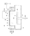
図1は、本発明の実施形態によるプラズマ処理方法に適用されるプラズマエッチング装置20の概略構成図である。図示するプラズマエッチング装置20は、NLD(磁気中性線放電:magnetic Neutral Loop Discharge)型のプラズマエッチング装置として構成されており、基板表面のエッチング機能と、基板表面のエッチングパターンの側壁部に保護膜を形成する機能とを兼ね備えている。
FIG. 1 is a schematic configuration diagram of a
図1において、21は真空槽であり、内部にプラズマ形成空間21aを含む真空チャンバ(プラズマチャンバ)が形成されている。真空槽21にはターボ分子ポンプ(TMP:Turbo Molecular Pump)等の真空ポンプが接続され、真空槽21の内部が所定の真空度に排気されている。
In FIG. 1,
プラズマ形成空間21aの周囲には、真空槽21の一部を構成する筒状壁22によって区画されている。筒状壁22は石英等の透明絶縁材料で構成されている。筒状壁22の外周側には、第1の高周波電源RF1に接続されたプラズマ発生用の高周波コイル(アンテナ)23と、この高周波コイル23の外周側に配置された三つの磁気コイル群24(24A,24B,24C)がそれぞれ配置されている。
A
磁気コイル24Aと磁気コイル24Cにはそれぞれ同一方向に電流が供給され、磁気コイル24Bには他の磁気コイル24A,24Cと逆方向に電流が供給される。その結果、プラズマ形成空間21aにおいて、磁場ゼロとなる磁気中性線25が環状に連続して形成される。そして、高周波コイル23により磁気中性線25に沿った誘導電場(高周波電場)が形成されることで、放電プラズマが形成される。
Current is supplied to the
特に、NLD方式のプラズマエッチング装置においては、磁気コイル24A〜24Cに流す電流の大きさによって、磁気中性線25の形成位置及び大きさ(半径)を調整することができる。すなわち、磁気コイル24A,24B,24Cに流す電流をそれぞれIA、IB、ICとしたとき、IA>ICの場合は磁気中性線25の形成位置は磁気コイル24C側へ下がり、逆に、IA<ICの場合は磁気中性線25の形成位置は磁気コイル24A側へ上がる。また、中間の磁気コイル24Bに流す電流IBを大きくすると、磁気中性線25のリング径は小さくなり、電流IBを小さくすると、磁気中性線25のリング径は大きくなる。さらに、電流IBの大きさで、磁気中性線25の磁場ゼロの位置での磁場勾配を制御することが可能であり、IBを大きくするほど磁場勾配が緩やかになり、IBを小さくするほど磁場勾配が急峻になる。これらの特性を利用することで、プラズマ密度分布の最適化を図ることができる。In particular, in the NLD plasma etching apparatus, the formation position and size (radius) of the magnetic
一方、真空槽21の内部には、半導体ウエハ(シリコン(Si)基板)Wを支持するステージ26が設置されている。ステージ26は、導電体を含む構成とされており、コンデンサ27を介して第2の高周波電源RF2に接続されている。なお、ステージ26には、基板Wを所定温度に加熱するためのヒータ等の加熱源が内蔵されている。
On the other hand, a
プラズマ形成空間21aの上部には、天板29が設置されている。天板29は、ステージ26の対向電極として構成されており、コンデンサ28を介して第3の高周波電源RF3に接続されている。天板29のプラズマ形成空間21a側の面には、スパッタにより基板を成膜するためのターゲット材(スパッタリングターゲット)30が取り付けられている。ターゲット材32は、本実施形態では、ポリテトラフルオロエチレン(PTFE)等のフッ素樹脂が用いられているが、これ以外の合成樹脂材料、あるいは珪素材、炭素材、炭化珪素材、酸化珪素材、窒化珪素材等が適用可能である。
A
天板29の近傍には、真空槽21の内部にプロセスガスを導入するためのガス導入管31が設置されている。本実施形態において、プロセスガスは、エッチング工程用のガス、スパッタ工程用のガスが含まれる。
In the vicinity of the
エッチングガスとしては、SF6、NF3、SiF4、XeF2の少なくとも何れか一種又は不活性ガスとの混合ガスが用いられる。混合ガスとしては、SF6/Ar、HBr/SF6/O2などの2種以上のガスの混合ガスを用いることができる。本実施形態では、エッチングガスとして、SF6/Arの混合ガスが用いられる。As the etching gas, SF 6 , NF 3 , SiF 4 , XeF 2 or a mixed gas with an inert gas is used. As the mixed gas, a mixed gas of two or more gases such as SF 6 / Ar, HBr / SF 6 / O 2 can be used. In the present embodiment, a mixed gas of SF 6 / Ar is used as the etching gas.
一方、スパッタ用のプロセスガスとしては、例えば、ArやN2等の希ガスあるいは不活性ガスを用いることができる。本実施形態では、スパッタ用のプロセスガスとして、Arが用いられる。On the other hand, as a process gas for sputtering, for example, a rare gas such as Ar or N 2 or an inert gas can be used. In the present embodiment, Ar is used as the sputtering process gas.
本実施形態のプラズマエッチング装置20においては、ステージ26上に載置された基板Wに対してエッチング工程と保護膜形成工程を交互に繰り返して行うことで、基板Wの表面に高アスペクト比の孔又はディープトレンチ等からなるビアを形成する。
In the
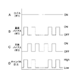
図2は、本実施形態のプラズマエッチング装置20の一動作例を示すタイミングチャートである。図2Aは、高周波コイル23に供給される第1の高周波電源RF1の電力印加タイミング、図2Bは、ステージ26に供給される第2の高周波電源RF2の電力印加タイミング、図2Cは、天板29に供給される第3の高周波電源RF3の電力印加タイミング、図2Dは、真空槽21の内部における圧力変化をそれぞれ示している。この例では、エッチング工程の処理圧力(プロセスガス導入量)は、保護膜形成工程のそれよりも高く設定されている。
FIG. 2 is a timing chart showing an operation example of the
基板Wの表面にはあらかじめ、マスクパターンが形成されている。このマスクパターンには、有機レジストやメタルマスク等のエッチングマスクが含まれる。エッチング工程及び保護膜形成工程では、プラズマ形成空間21aに、磁気コイル群24による環状磁気中性線25が形成され、更に、第1の高周波電源RF1から高周波コイル23への電力投入により、環状磁気中性線25に沿って誘導結合プラズマが形成される。
A mask pattern is formed in advance on the surface of the substrate W. This mask pattern includes an etching mask such as an organic resist or a metal mask. In the etching process and the protective film forming process, an annular magnetic
エッチング工程において、真空槽21の内部に導入されたエッチングガス(SF6とArの混合ガス)は、プラズマ形成空間21aでプラズマ化し、生成されたイオンとラジカルによりステージ26上の基板Wをエッチング処理する。このとき、第2の高周波電源RF2からの電力投入で基板バイアスがONとなり、イオンをステージ26側へ加速させ、基板W上のラジカル生成物をスパッタ除去してエッチング性を高める。すなわち、フッ素ラジカルがシリコンと反応してラジカル生成物を形成し、これをプラズマ中のイオンによるスパッタ作用で除去することで、シリコン基板Wのエッチング処理が進行する。In the etching process, the etching gas (mixed gas of SF 6 and Ar) introduced into the
一方、エッチング処理を所定時間行った後、真空槽21の内部に残留するエッチングガスが排気される。そして、保護膜形成用のプロセスガス(Ar)が真空槽21の内部に導入されることで保護膜形成工程が開始される。導入されたプロセスガスは、プラズマ形成空間21aでプラズマ化される。このとき、基板バイアス(RF2)はOFFとなり、代わりに、第3の高周波電源(RF3)からの電力投入で天板バイアスがONとなる。その結果、天板29に設置されたターゲット材30はプラズマ中のイオンによりスパッタされ、そのスパッタ物が基板Wの表面及び上述のエッチング工程で形成されたエッチングパターンに付着する。以上のようにして、エッチングパターンの底部及び側壁部に、保護膜として機能するポリマー層が形成される。
On the other hand, after the etching process is performed for a predetermined time, the etching gas remaining in the
ここで、ターゲット材30から叩き出されたスパッタ粒子は、プラズマ形成空間21aに形成されているNLDプラズマを通過して基板へ到達する。このとき、スパッタ粒子は、環状磁気中性線25が形成される高密度プラズマ領域で分解、再励起されることにより、化学的蒸着法(CVD法)に類似する成膜形態で、基板の表面に対して等方的に入射する。したがって、本実施形態によって得られるエッチングパターンの段差被覆(保護膜)は、カバレッジ性が高く、面内均一性に優れる。
Here, the sputtered particles knocked out from the
なお、保護膜形成工程のプロセスガスとして、例えばArとフロロカーボン系ガス(C4F8、CHF3等)の混合ガスを用いることで、プロセスガス中の反応ガスがプラズマ形成空間21aにおいてプラズマ化し、そのラジカル生成物が基板表面に堆積することによって、保護膜として機能するポリマー層を形成することが可能である。更に、プロセスガスとして上記混合ガスを用いることで、Arガスのみをプロセスガスとして用いる場合に比べてスパッタレートの向上を図ることができる。As a process gas in the protective film formation step, for example, a mixed gas of Ar and fluorocarbon-based gas (C 4 F 8 , CHF 3 or the like) is used, so that the reaction gas in the process gas is converted into plasma in the
保護膜形成工程を所定時間行った後、再び上述したエッチング工程が行われる。このエッチング工程の初期段階は、エッチングパターンの底部を被覆する保護膜の除去作用に費やされる。その後、保護膜の除去により露出したエッチングパターンの底部のエッチング処理が再開される。このとき、プラズマ中のイオンは、基板バイアス作用によって基板に対して垂直方向に入射する。このため、エッチングパターンの側壁部を被覆する保護膜に到達するイオンは、エッチングパターンの底部に到達するイオンに比べて少ない。したがって、エッチング工程の間、エッチングパターンの側壁部を被覆する保護膜は完全に除去されることなく残留する。これにより、エッチングパターンの側壁部とフッ素ラジカルとの接触が回避され、エッチングパターンの側壁部のエッチングによる侵食が回避される。 After performing the protective film forming process for a predetermined time, the above-described etching process is performed again. The initial stage of this etching process is spent on the removal of the protective film that covers the bottom of the etching pattern. Thereafter, the etching process of the bottom of the etching pattern exposed by removing the protective film is resumed. At this time, ions in the plasma are incident on the substrate in the vertical direction by the substrate bias action. For this reason, the number of ions reaching the protective film covering the side wall of the etching pattern is less than the number of ions reaching the bottom of the etching pattern. Therefore, during the etching process, the protective film covering the side wall of the etching pattern remains without being completely removed. As a result, contact between the sidewall portion of the etching pattern and the fluorine radical is avoided, and erosion due to etching of the sidewall portion of the etching pattern is avoided.
以降、上述のエッチング工程と保護膜形成工程が交互に繰り返し行われることで、基板表面に対して垂直方向の異方性エッチングが実現される。以上のようにして、基板Wの内部に高アスペクト比のビア(コンタクトホール、トレンチ)が作製される。 Thereafter, anisotropic etching in the direction perpendicular to the substrate surface is realized by alternately and repeatedly performing the above-described etching step and protective film forming step. As described above, high aspect ratio vias (contact holes, trenches) are formed inside the substrate W.
ところで、基板の表面をエッチング又はスパッタ成膜する際には、基板の表面に対するこれらのプラズマ処理の面内均一性の確保が重要である。このことは、基板のサイズが大型化するほど顕著となる。面内均一性は、真空槽内に形成されるプラズマの位置すなわち密度分布に強く依存する。磁気中性線放電(NLD)は、磁気中性線の形成位置で高密度のプラズマが形成される。したがって、磁気中性線の半径を変化させることで、真空槽内に発生するプラズマの密度分布が可変となる。本実施形態においては、磁気中性線25の半径は、磁気コイル群24の中央の磁気コイル24Bへ供給する電流の大きさによって調整することができる。
By the way, when performing etching or sputtering film formation on the surface of the substrate, it is important to ensure in-plane uniformity of these plasma treatments on the surface of the substrate. This becomes more significant as the size of the substrate increases. The in-plane uniformity strongly depends on the position of plasma formed in the vacuum chamber, that is, the density distribution. In the magnetic neutral line discharge (NLD), high-density plasma is formed at the position where the magnetic neutral line is formed. Therefore, the density distribution of plasma generated in the vacuum chamber can be varied by changing the radius of the magnetic neutral line. In the present embodiment, the radius of the magnetic
また、プラズマの形成位置は、スパッタ条件やエッチング条件などによっても面内均一性に大きな影響を与える。その一例として、スパッタ条件、導入ガスの圧力、導入ガスの混合比、アンテナパワー(RF1)の各々に関するプラズマ形成位置と基板の面内均一性との関係を図3に示す。 In addition, the plasma formation position greatly affects the in-plane uniformity depending on sputtering conditions, etching conditions, and the like. As an example, FIG. 3 shows the relationship between the plasma formation position and the in-plane uniformity of the substrate for each of sputtering conditions, introduced gas pressure, introduced gas mixture ratio, and antenna power (RF1).
図3において、横軸の「NL電流値」は、磁気コイル群24(図1)の中央の磁気コイル24Bへ供給する電流の大きさを示している。この電流値が大きくなるほど磁気中性線25の半径は小さくなり、電流値が小さくなるほど磁気中性線25の半径は大きくなる。図中「スパッタ条件」は、ガス圧、ガス混合比、アンテナパワー(RF1)、天板バイアスパワー(RF3)などの各種パラメータが含まれている。なお、図3において「スパッタ条件」、「ガス圧」、「ガス混合比」、「アンテナパワー」はそれぞれ固定値であり、図3は、これらの固定値に対するNL電流値と面内均一性との関係を示している。
In FIG. 3, the “NL current value” on the horizontal axis indicates the magnitude of the current supplied to the central
図3に示したように、スパッタ条件、ガス圧、ガス混合比、アンテナパワーなどは、面内均一性に大きな関連を有している。図示せずとも、エッチング条件に関しても同様である。したがって、スパッタ処理及びエッチング処理に際しては、所望の面内均一性を確保する観点から、最適なプラズマ分布密度を設定する必要がある。 As shown in FIG. 3, sputtering conditions, gas pressure, gas mixture ratio, antenna power, and the like have a great relationship with in-plane uniformity. Although not shown, the same applies to the etching conditions. Therefore, in the sputtering process and the etching process, it is necessary to set an optimum plasma distribution density from the viewpoint of ensuring a desired in-plane uniformity.
そこで、本実施形態においては、基板Wに対するエッチング(プラズマ処理)の進行に応じて、磁気中性線25の半径を変化させるようにしている。例えば、基板中央部が周縁部に比べてエッチングレートが高い場合、環状磁気中性線の半径を大きくしてエッチングレートの面内均一性を向上させる。
Therefore, in the present embodiment, the radius of the magnetic
例えば、図4(A)〜(C)に示すように、基板W上の一部のエッチングパターンP2,P3がこれらよりも外周側のエッチングパターンP1又は内周側のエッチングパターンP4よりもエッチングレートが速い場合、適宜のタイミングで磁気中性線25の半径を変化させる。この場合、磁気中性線25の半径を小さくしたり、大きくしたりすることで、パターンP1,P4のエッチングレートをパターンP2,P3のエッチングレートに合致させることができる。なお図4において、参照符号Mは、基板Wの表面に形成されたエッチング用のマスクパターンである。
For example, as shown in FIGS. 4A to 4C, a part of the etching patterns P2 and P3 on the substrate W has an etching rate higher than the etching pattern P1 on the outer peripheral side or the etching pattern P4 on the inner peripheral side. Is fast, the radius of the magnetic
上述した方法は、1つのエッチング工程内で磁気中性線25の半径を多段階に変化させる制御を採用してもよいし、スパッタ工程からエッチング工程へ切り換えられる毎に磁気中性線25の半径を変化させる制御を採用してもよい。また、磁気中性線25の半径の変化は、予め設定した半径の大きさで多段階に変化させる制御だけに限られず、予め設定した半径の大きさの範囲内で連続的に変化させる制御も含まれる。
The above-described method may adopt a control in which the radius of the magnetic
基板Wに対するエッチング(プラズマ処理)の進行に応じて磁気中性線25の半径を変化させる他の制御例としては、エッチング工程とスパッタ工程とで磁気中性線の形成位置を変化させる制御が挙げられる。エッチング工程とスパッタ工程とで所望の面内均一性を確保できるプラズマ形成位置がそれぞれ異なる場合があるからである。この場合、エッチング工程及びスパッタ工程のそれぞれの磁気中性線の半径(NL電流値)の最適値を予め取得しておき、エッチング処理とスパッタ処理の切換時に、磁気中性線の半径をそれぞれの最適値に変化させる。これにより、エッチング処理時及びスパッタ処理時のそれぞれにおいて所望の面内均一性を確保することが可能となる。
As another example of control for changing the radius of the magnetic
一方、エッチングパターンの深さに応じてエッチングレートの面内分布が変化することから、エッチングレートの面内分布に対応させて磁気中性線の半径を変化させることができる。これにより、エッチングパターンの深さに応じた、面内均一性に優れた最適なプラズマ分布密度を提供することが可能となる。また必要に応じて、磁気中性線の高さ位置や磁場勾配を変化させてもよい。 On the other hand, since the in-plane distribution of the etching rate changes according to the depth of the etching pattern, the radius of the magnetic neutral line can be changed in accordance with the in-plane distribution of the etching rate. This makes it possible to provide an optimal plasma distribution density with excellent in-plane uniformity according to the depth of the etching pattern. Moreover, you may change the height position and magnetic field gradient of a magnetic neutral line as needed.
このように、エッチング開始から終了までの間を複数の段階に区分し、各段階においてあらかじめ評価しておいた最適なプロセス条件に適合するように磁気中性線25の半径を変化させることで、エッチング(プラズマ処理)開始から終了までの間にわたり、面内均一性に優れたエッチングを行うことが可能となる。区分する段階数は特に限定されないが、段階数が多いほど高精度なエッチング加工を実現することができる。
In this way, the period from the start to the end of etching is divided into a plurality of stages, and by changing the radius of the magnetic
上述したような磁気中性線25の半径制御に加えて、さらに、以下に挙げるパラメータについても変化させることによって、エッチング面内均一性の向上を図ることが可能となる。
In addition to the radius control of the magnetic
(ガス圧)
エッチング(プラズマ処理)の開始から終了までの間にわたって、真空槽21内へ導入するガスの圧力を段階的に変化させる。例えば、エッチング開始時は、ガス圧を比較的高めに設定し、エッチングの進行に応じてガス圧を低下させる制御を採用することができる。(Gas pressure)
The pressure of the gas introduced into the
通常、シリコン基板の深掘りエッチングでは、エッチングパターンが深くなるに従い、パターンの開口部のエッチングも進行することから、パターン開口部の形状精度を維持することが困難となる。そこで、エッチングの進行に応じてガス圧を低下させることで、パターンの底部へ向かうイオンの指向性を強めて、基板垂直方向に向かうエッチング異方性を高めることができる。これにより、パターン開口部の形状精度に優れた深掘り加工を実現することが可能となる。 Usually, in the deep etching of a silicon substrate, as the etching pattern becomes deeper, the etching of the opening of the pattern also proceeds, so that it is difficult to maintain the shape accuracy of the pattern opening. Therefore, by reducing the gas pressure in accordance with the progress of etching, the directivity of ions toward the bottom of the pattern can be increased, and the etching anisotropy toward the substrate vertical direction can be increased. Thereby, it is possible to realize deep digging with excellent shape accuracy of the pattern opening.
なお、このガス圧制御は、エッチング工程及びスパッタ工程においてそれぞれ実施可能である。 This gas pressure control can be carried out in the etching process and the sputtering process, respectively.
(ガス混合比)
エッチング(プラズマ処理)の開始から終了までの間にわたって、真空槽21内へ導入するエッチングガス(SF6/Ar)の混合比を変化させる。例えば、エッチングの進行に応じてエッチングガス中のAr量を増加させる。(Gas mixing ratio)
The mixing ratio of the etching gas (SF 6 / Ar) introduced into the
シリコン基板の深掘りエッチングでは、比較的高いエッチングレートが得られることから、SF6などのフッ素系ガスがエッチングガスとして多用されている。しかし、フッ素系ガスによるシリコンのエッチングは等方性が強いため、パターンが深くなるに従って、パターン開口部の形状精度の劣化や、パターン底部へ到達するイオン量の低下が顕在化する。そこで、エッチングの進行に応じてガス中のAr含有量を増加させることで、パターンの底部へ向かうイオンの量を増加させて所望のエッチングレートを確保するとともに、パターン開口部の形状精度の劣化を効果的に防止することが可能となる。In the deep etching of a silicon substrate, a relatively high etching rate can be obtained, so that a fluorine-based gas such as SF 6 is frequently used as an etching gas. However, since etching of silicon with a fluorine-based gas is highly isotropic, deterioration of the shape accuracy of the pattern opening and a decrease in the amount of ions reaching the bottom of the pattern become apparent as the pattern becomes deeper. Therefore, by increasing the Ar content in the gas as the etching progresses, the amount of ions toward the bottom of the pattern is increased to ensure a desired etching rate, and the shape accuracy of the pattern opening is degraded. It can be effectively prevented.
(アンテナパワー)
エッチング(プラズマ処理)の開始から終了までの間にわたって、磁気中性線25に沿って形成されるプラズマの強度をアンテナパワーの制御によって段階的に変化させる。(Antenna power)
From the start to the end of etching (plasma treatment), the intensity of the plasma formed along the magnetic
上述のように、プラズマの分布密度は、基板の面内均一性に大きな影響を与える。プラズマの分布密度は、磁気中性線25の半径の大きさだけでなく、プラズマを発生させるアンテナパワーすなわち高周波コイル23へ印加する高周波電力(RF1)の大きさにも大きく関連する。したがって、磁気中性線25の半径制御に加えて、アンテナパワーの大きさも適宜調整することによって、面内分布の均一性のさらなる向上を図ることができるとともに、面内均一制御を容易に実現することができる。
As described above, the plasma distribution density greatly affects the in-plane uniformity of the substrate. The plasma distribution density is greatly related not only to the size of the radius of the magnetic
アンテナパワーとエッチング種の量はほぼ比例関係にあることから、アンテナパワーを固定した場合、エッチングの進行に伴ってパターン開口部の侵食も顕在化する傾向にある。そこで、エッチングの進行に応じてアンテナパワーを低下させることにより、パターン開口部のエッチングダメージの低減を図りながら、パターン底部に対する所定のエッチング効果を維持することが可能となる。また、エッチングの進行に応じて、ステージ26へ印加するバイアスパワー(RF2)を上昇させるようにすれば、パターンの底部へ到達するイオンの量が高まるため、エッチングレートの大幅な低下を回避することが可能となる。
Since the antenna power and the amount of etching species are in a substantially proportional relationship, when the antenna power is fixed, the erosion of the pattern opening tends to become apparent as the etching progresses. Therefore, by reducing the antenna power according to the progress of etching, it is possible to maintain a predetermined etching effect on the pattern bottom while reducing etching damage at the pattern opening. Further, if the bias power (RF2) applied to the
以上、本発明の実施形態について説明したが、本発明は上述の実施形態にのみ限定されるものではなく、本発明の要旨を逸脱しない範囲内において種々変更を加え得ることは勿論である。 The embodiment of the present invention has been described above, but the present invention is not limited to the above-described embodiment, and it is needless to say that various modifications can be made without departing from the gist of the present invention.
例えば、エッチング(プラズマ処理)の進行に応じて段階的に変化させる制御パラメータは、上述したアンテナパワーや導入ガス圧、ガス混合比だけでなく、ステージ26に印加するバイアス電力(RF2)や天板29に印加するバイアス電力(RF3)にも適用することが可能である。例えば、前者の場合には、エッチングの進行に応じてバイアスパワー(RF2)を増加させる。これにより、パターン底部へのイオンの引き込み作用を高めて高いエッチングレートを確保できる。
For example, control parameters that are changed stepwise in accordance with the progress of etching (plasma processing) include not only the antenna power, the introduced gas pressure, and the gas mixture ratio, but also the bias power (RF2) applied to the
20 プラズマエッチング装置
21 真空槽
23 高周波コイル(アンテナ)
24 磁気コイル群
25 磁気中性線
26 ステージ
29 天板
30 ターゲット材
31 ガス導入管
W 基板20
24
Claims (8)
前記真空槽内で、前記プラズマを用いて表面にマスクパターンが形成された基板をエッチングし、
前記真空槽内に設置されたターゲット材を前記プラズマでスパッタすることで、前記基板に形成されたエッチングパターンの側壁部に保護膜を形成し、
前記エッチングパターンの深さに応じて前記磁気中性線の半径を変化させる
プラズマ処理方法。 By generating a high-frequency electric field along the annular magnetic neutral line formed in the vacuum chamber, the plasma of the gas introduced into the vacuum chamber is generated,
In the vacuum chamber, etching the substrate having a mask pattern formed on the surface using the plasma,
Sputtering the target material installed in the vacuum chamber with the plasma to form a protective film on the side wall of the etching pattern formed on the substrate,
A plasma processing method, wherein a radius of the magnetic neutral line is changed according to a depth of the etching pattern .
前記磁気中性線の半径を変化させる工程は、前記基板の中央部のエッチングレートが前記基板の周縁部のエッチングレートよりも速い場合には、前記磁気中性線の半径を大きくし、前記中央部のエッチングレートが前記周縁部のエッチングレートよりも遅い場合には、前記磁気中性線の半径を小さくするThe step of changing the radius of the magnetic neutral line increases the radius of the magnetic neutral line when the etching rate of the central part of the substrate is faster than the etching rate of the peripheral part of the substrate. If the etching rate of the part is slower than the etching rate of the peripheral part, the radius of the magnetic neutral line is reduced.
プラズマ処理方法。Plasma processing method.
前記基板をエッチングする工程と前記保護膜を形成する工程は、交互に繰り返して実施され、
前記磁気中性線の半径を変化させる工程は、前記プラズマ処理の開始から終了までの間、前記磁気中性線の半径を段階的に変化させる
プラズマ処理方法。 The plasma processing method according to claim 1,
The step of etching the substrate and the step of forming the protective film are alternately repeated,
The step of changing the radius of the magnetic neutral line changes the radius of the magnetic neutral line stepwise from the start to the end of the plasma processing.
前記磁気中性線の半径を変化させる工程は、前記基板をエッチングする工程で実施される
プラズマ処理方法。 The plasma processing method according to claim 3 ,
The step of changing the radius of the magnetic neutral line is performed in the step of etching the substrate.
前記磁気中性線の半径を変化させる工程は、前記保護膜を形成する工程で実施される
プラズマ処理方法。 The plasma processing method according to claim 3 ,
The step of changing the radius of the magnetic neutral line is performed in the step of forming the protective film.
前記基板に対するプラズマ処理の進行に応じて、前記ガスの圧力を変化させる
プラズマ処理方法。 The plasma processing method according to claim 1, further comprising:
A plasma processing method, wherein the pressure of the gas is changed according to the progress of plasma processing on the substrate.
前記ガスは、2種以上の混合ガスであり、
前記プラズマ処理方法は、さらに、
前記基板に対するプラズマ処理の進行に応じて、前記ガスの混合比を変化させる
プラズマ処理方法。 The plasma processing method according to claim 1,
The gas is a mixed gas of two or more kinds,
The plasma processing method further includes:
A plasma processing method for changing a mixing ratio of the gas in accordance with progress of plasma processing on the substrate.
前記基板に対するプラズマ処理の進行に応じて、前記高周波電場の強さを変化させる
プラズマ処理方法。 The plasma processing method according to claim 1, further comprising:
A plasma processing method, wherein intensity of the high-frequency electric field is changed according to progress of plasma processing on the substrate.
Priority Applications (1)
| Application Number | Priority Date | Filing Date | Title |
|---|---|---|---|
| JP2010501961A JP5367689B2 (en) | 2008-03-07 | 2009-03-05 | Plasma processing method |
Applications Claiming Priority (4)
| Application Number | Priority Date | Filing Date | Title |
|---|---|---|---|
| JP2008057621 | 2008-03-07 | ||
| JP2008057621 | 2008-03-07 | ||
| JP2010501961A JP5367689B2 (en) | 2008-03-07 | 2009-03-05 | Plasma processing method |
| PCT/JP2009/054205 WO2009110567A1 (en) | 2008-03-07 | 2009-03-05 | Plasma processing method |
Publications (2)
| Publication Number | Publication Date |
|---|---|
| JPWO2009110567A1 JPWO2009110567A1 (en) | 2011-07-14 |
| JP5367689B2 true JP5367689B2 (en) | 2013-12-11 |
Family
ID=41056119
Family Applications (1)
| Application Number | Title | Priority Date | Filing Date |
|---|---|---|---|
| JP2010501961A Active JP5367689B2 (en) | 2008-03-07 | 2009-03-05 | Plasma processing method |
Country Status (7)
| Country | Link |
|---|---|
| US (1) | US20110117742A1 (en) |
| EP (1) | EP2267764A4 (en) |
| JP (1) | JP5367689B2 (en) |
| KR (1) | KR101189847B1 (en) |
| CN (1) | CN101960569B (en) |
| TW (1) | TWI446439B (en) |
| WO (1) | WO2009110567A1 (en) |
Families Citing this family (7)
| Publication number | Priority date | Publication date | Assignee | Title |
|---|---|---|---|---|
| JPWO2011018900A1 (en) * | 2009-08-14 | 2013-01-17 | 株式会社アルバック | Etching method |
| JP5800532B2 (en) * | 2011-03-03 | 2015-10-28 | 東京エレクトロン株式会社 | Plasma processing apparatus and plasma processing method |
| JP6173086B2 (en) * | 2013-07-19 | 2017-08-02 | キヤノン株式会社 | Etching method of silicon substrate |
| CN104347393A (en) * | 2013-07-30 | 2015-02-11 | 中芯国际集成电路制造(上海)有限公司 | Method for removing natural oxidation layer at bottom of contact window |
| JP6316735B2 (en) * | 2014-12-04 | 2018-04-25 | 東京エレクトロン株式会社 | Plasma etching method |
| JP7008474B2 (en) * | 2016-11-30 | 2022-01-25 | 東京エレクトロン株式会社 | Plasma etching method |
| WO2020121540A1 (en) * | 2019-02-04 | 2020-06-18 | 株式会社日立ハイテク | Plasma processing method and plasma processing device |
Citations (3)
| Publication number | Priority date | Publication date | Assignee | Title |
|---|---|---|---|---|
| JPH0790632A (en) * | 1993-07-26 | 1995-04-04 | Ulvac Japan Ltd | Electric discharge plasma treating device |
| JPH0963792A (en) * | 1995-08-25 | 1997-03-07 | Ulvac Japan Ltd | Magnetic neutral beam discharging plasma source |
| WO2006003962A1 (en) * | 2004-07-02 | 2006-01-12 | Ulvac, Inc. | Etching method and system |
Family Cites Families (6)
| Publication number | Priority date | Publication date | Assignee | Title |
|---|---|---|---|---|
| US6475333B1 (en) * | 1993-07-26 | 2002-11-05 | Nihon Shinku Gijutsu Kabushiki Kaisha | Discharge plasma processing device |
| DE10326135B4 (en) * | 2002-06-12 | 2014-12-24 | Ulvac, Inc. | A discharge plasma processing system |
| JP4246591B2 (en) * | 2003-10-08 | 2009-04-02 | 日本電信電話株式会社 | Dry etching equipment |
| US7556718B2 (en) * | 2004-06-22 | 2009-07-07 | Tokyo Electron Limited | Highly ionized PVD with moving magnetic field envelope for uniform coverage of feature structure and wafer |
| JP4646053B2 (en) * | 2004-09-29 | 2011-03-09 | 株式会社アルバック | Branch switch and etching apparatus for high frequency power |
| WO2009020129A1 (en) * | 2007-08-08 | 2009-02-12 | Ulvac, Inc. | Plasma processing method and plasma processing apparatus |
-
2009
- 2009-03-05 WO PCT/JP2009/054205 patent/WO2009110567A1/en active Application Filing
- 2009-03-05 EP EP09718527A patent/EP2267764A4/en not_active Withdrawn
- 2009-03-05 KR KR1020107019298A patent/KR101189847B1/en active IP Right Grant
- 2009-03-05 JP JP2010501961A patent/JP5367689B2/en active Active
- 2009-03-05 US US12/920,925 patent/US20110117742A1/en not_active Abandoned
- 2009-03-05 CN CN2009801071603A patent/CN101960569B/en active Active
- 2009-03-06 TW TW098107274A patent/TWI446439B/en active
Patent Citations (3)
| Publication number | Priority date | Publication date | Assignee | Title |
|---|---|---|---|---|
| JPH0790632A (en) * | 1993-07-26 | 1995-04-04 | Ulvac Japan Ltd | Electric discharge plasma treating device |
| JPH0963792A (en) * | 1995-08-25 | 1997-03-07 | Ulvac Japan Ltd | Magnetic neutral beam discharging plasma source |
| WO2006003962A1 (en) * | 2004-07-02 | 2006-01-12 | Ulvac, Inc. | Etching method and system |
Also Published As
| Publication number | Publication date |
|---|---|
| TWI446439B (en) | 2014-07-21 |
| EP2267764A1 (en) | 2010-12-29 |
| JPWO2009110567A1 (en) | 2011-07-14 |
| EP2267764A4 (en) | 2011-05-04 |
| TW200947549A (en) | 2009-11-16 |
| KR20100110886A (en) | 2010-10-13 |
| US20110117742A1 (en) | 2011-05-19 |
| CN101960569A (en) | 2011-01-26 |
| WO2009110567A1 (en) | 2009-09-11 |
| KR101189847B1 (en) | 2012-10-10 |
| CN101960569B (en) | 2012-11-28 |
Similar Documents
| Publication | Publication Date | Title |
|---|---|---|
| JP5207406B2 (en) | Plasma processing method | |
| JP4657458B2 (en) | Techniques for etching low-capacity dielectric layers | |
| JP5367689B2 (en) | Plasma processing method | |
| US9054050B2 (en) | Method for deep silicon etching using gas pulsing | |
| JP3527901B2 (en) | Plasma etching method | |
| JP2010021442A (en) | Plasma processing method and apparatus | |
| KR102513051B1 (en) | Etching method | |
| KR102363778B1 (en) | Etching method | |
| US20220181162A1 (en) | Etching apparatus | |
| JP2012142495A (en) | Plasma etching method and plasma etching apparatus | |
| JP6180824B2 (en) | Plasma etching method and plasma etching apparatus | |
| JP2004296474A (en) | Silicon substrate etching method and etching apparatus | |
| JP5851349B2 (en) | Plasma etching method and plasma etching apparatus | |
| JP6504827B2 (en) | Etching method | |
| JP5060869B2 (en) | Plasma processing equipment | |
| JP2014220387A (en) | Plasma etching method | |
| JP5065726B2 (en) | Dry etching method | |
| US6737358B2 (en) | Plasma etching uniformity control | |
| JP2005123550A (en) | Anisotropic etching method | |
| JP5774356B2 (en) | Plasma processing method | |
| JP2017143194A (en) | Semiconductor element manufacturing method | |
| JP2006114933A (en) | Reactive ion etching device | |
| JP5284679B2 (en) | Plasma etching method | |
| JP4958658B2 (en) | Plasma processing method | |
| JP6228860B2 (en) | Manufacturing method of semiconductor device |
Legal Events
| Date | Code | Title | Description |
|---|---|---|---|
| A131 | Notification of reasons for refusal |
Free format text: JAPANESE INTERMEDIATE CODE: A131 Effective date: 20121002 |
|
| A521 | Request for written amendment filed |
Free format text: JAPANESE INTERMEDIATE CODE: A523 Effective date: 20121127 |
|
| TRDD | Decision of grant or rejection written | ||
| A01 | Written decision to grant a patent or to grant a registration (utility model) |
Free format text: JAPANESE INTERMEDIATE CODE: A01 Effective date: 20130827 |
|
| A61 | First payment of annual fees (during grant procedure) |
Free format text: JAPANESE INTERMEDIATE CODE: A61 Effective date: 20130911 |
|
| R150 | Certificate of patent or registration of utility model |
Ref document number: 5367689 Country of ref document: JP Free format text: JAPANESE INTERMEDIATE CODE: R150 Free format text: JAPANESE INTERMEDIATE CODE: R150 |
|
| R250 | Receipt of annual fees |
Free format text: JAPANESE INTERMEDIATE CODE: R250 |
|
| R250 | Receipt of annual fees |
Free format text: JAPANESE INTERMEDIATE CODE: R250 |
|
| R250 | Receipt of annual fees |
Free format text: JAPANESE INTERMEDIATE CODE: R250 |
|
| R250 | Receipt of annual fees |
Free format text: JAPANESE INTERMEDIATE CODE: R250 |
|
| R250 | Receipt of annual fees |
Free format text: JAPANESE INTERMEDIATE CODE: R250 |
|
| R250 | Receipt of annual fees |
Free format text: JAPANESE INTERMEDIATE CODE: R250 |
|
| R250 | Receipt of annual fees |
Free format text: JAPANESE INTERMEDIATE CODE: R250 |
|
| R250 | Receipt of annual fees |
Free format text: JAPANESE INTERMEDIATE CODE: R250 |