JP2021034487A - Method for processing substrate, method for manufacturing device, and plasma processing device - Google Patents
Method for processing substrate, method for manufacturing device, and plasma processing device Download PDFInfo
- Publication number
- JP2021034487A JP2021034487A JP2019151441A JP2019151441A JP2021034487A JP 2021034487 A JP2021034487 A JP 2021034487A JP 2019151441 A JP2019151441 A JP 2019151441A JP 2019151441 A JP2019151441 A JP 2019151441A JP 2021034487 A JP2021034487 A JP 2021034487A
- Authority
- JP
- Japan
- Prior art keywords
- plasma
- substrate
- chamber
- upper electrode
- gas
- Prior art date
- Legal status (The legal status is an assumption and is not a legal conclusion. Google has not performed a legal analysis and makes no representation as to the accuracy of the status listed.)
- Pending
Links
- 238000012545 processing Methods 0.000 title claims abstract description 88
- 239000000758 substrate Substances 0.000 title claims abstract description 81
- 238000000034 method Methods 0.000 title claims abstract description 49
- 238000004519 manufacturing process Methods 0.000 title claims description 6
- XUIMIQQOPSSXEZ-UHFFFAOYSA-N Silicon Chemical compound [Si] XUIMIQQOPSSXEZ-UHFFFAOYSA-N 0.000 claims abstract description 23
- 229910052710 silicon Inorganic materials 0.000 claims abstract description 23
- 239000010703 silicon Substances 0.000 claims abstract description 23
- 150000002500 ions Chemical class 0.000 claims abstract description 18
- 239000000126 substance Substances 0.000 claims abstract description 5
- 239000007789 gas Substances 0.000 claims description 78
- XKRFYHLGVUSROY-UHFFFAOYSA-N Argon Chemical compound [Ar] XKRFYHLGVUSROY-UHFFFAOYSA-N 0.000 claims description 8
- UFHFLCQGNIYNRP-UHFFFAOYSA-N Hydrogen Chemical compound [H][H] UFHFLCQGNIYNRP-UHFFFAOYSA-N 0.000 claims description 5
- IJGRMHOSHXDMSA-UHFFFAOYSA-N Atomic nitrogen Chemical compound N#N IJGRMHOSHXDMSA-UHFFFAOYSA-N 0.000 claims description 4
- 229910052786 argon Inorganic materials 0.000 claims description 4
- 229910001873 dinitrogen Inorganic materials 0.000 claims description 4
- 238000005530 etching Methods 0.000 claims description 2
- 239000012528 membrane Substances 0.000 description 26
- 238000001020 plasma etching Methods 0.000 description 19
- 238000002474 experimental method Methods 0.000 description 18
- 239000000463 material Substances 0.000 description 10
- XAGFODPZIPBFFR-UHFFFAOYSA-N aluminium Chemical compound [Al] XAGFODPZIPBFFR-UHFFFAOYSA-N 0.000 description 6
- 229910052782 aluminium Inorganic materials 0.000 description 6
- 238000005260 corrosion Methods 0.000 description 6
- 230000007797 corrosion Effects 0.000 description 6
- VYPSYNLAJGMNEJ-UHFFFAOYSA-N Silicium dioxide Chemical compound O=[Si]=O VYPSYNLAJGMNEJ-UHFFFAOYSA-N 0.000 description 5
- 239000004020 conductor Substances 0.000 description 4
- 229910052814 silicon oxide Inorganic materials 0.000 description 4
- 239000000919 ceramic Substances 0.000 description 3
- 238000009792 diffusion process Methods 0.000 description 3
- SIWVEOZUMHYXCS-UHFFFAOYSA-N oxo(oxoyttriooxy)yttrium Chemical compound O=[Y]O[Y]=O SIWVEOZUMHYXCS-UHFFFAOYSA-N 0.000 description 3
- 238000009832 plasma treatment Methods 0.000 description 3
- 238000012546 transfer Methods 0.000 description 3
- 230000007423 decrease Effects 0.000 description 2
- 238000010586 diagram Methods 0.000 description 2
- NBVXSUQYWXRMNV-UHFFFAOYSA-N fluoromethane Chemical compound FC NBVXSUQYWXRMNV-UHFFFAOYSA-N 0.000 description 2
- 239000011810 insulating material Substances 0.000 description 2
- 230000000737 periodic effect Effects 0.000 description 2
- 229920002120 photoresistant polymer Polymers 0.000 description 2
- HBMJWWWQQXIZIP-UHFFFAOYSA-N silicon carbide Chemical compound [Si+]#[C-] HBMJWWWQQXIZIP-UHFFFAOYSA-N 0.000 description 2
- 229910010271 silicon carbide Inorganic materials 0.000 description 2
- YCKRFDGAMUMZLT-UHFFFAOYSA-N Fluorine atom Chemical compound [F] YCKRFDGAMUMZLT-UHFFFAOYSA-N 0.000 description 1
- QVGXLLKOCUKJST-UHFFFAOYSA-N atomic oxygen Chemical compound [O] QVGXLLKOCUKJST-UHFFFAOYSA-N 0.000 description 1
- 239000006227 byproduct Substances 0.000 description 1
- 230000001276 controlling effect Effects 0.000 description 1
- 239000003989 dielectric material Substances 0.000 description 1
- 238000011156 evaluation Methods 0.000 description 1
- 229910052731 fluorine Inorganic materials 0.000 description 1
- 239000011737 fluorine Substances 0.000 description 1
- 238000012986 modification Methods 0.000 description 1
- 230000004048 modification Effects 0.000 description 1
- 239000011368 organic material Substances 0.000 description 1
- TWNQGVIAIRXVLR-UHFFFAOYSA-N oxo(oxoalumanyloxy)alumane Chemical compound O=[Al]O[Al]=O TWNQGVIAIRXVLR-UHFFFAOYSA-N 0.000 description 1
- 239000001301 oxygen Substances 0.000 description 1
- 229910052760 oxygen Inorganic materials 0.000 description 1
- 238000000206 photolithography Methods 0.000 description 1
- 239000010453 quartz Substances 0.000 description 1
- 239000003507 refrigerant Substances 0.000 description 1
- 230000001105 regulatory effect Effects 0.000 description 1
- 239000002356 single layer Substances 0.000 description 1
- 238000006467 substitution reaction Methods 0.000 description 1
Images


Classifications
-
- H—ELECTRICITY
- H01—ELECTRIC ELEMENTS
- H01L—SEMICONDUCTOR DEVICES NOT COVERED BY CLASS H10
- H01L21/00—Processes or apparatus adapted for the manufacture or treatment of semiconductor or solid state devices or of parts thereof
- H01L21/02—Manufacture or treatment of semiconductor devices or of parts thereof
- H01L21/027—Making masks on semiconductor bodies for further photolithographic processing not provided for in group H01L21/18 or H01L21/34
- H01L21/0271—Making masks on semiconductor bodies for further photolithographic processing not provided for in group H01L21/18 or H01L21/34 comprising organic layers
- H01L21/0273—Making masks on semiconductor bodies for further photolithographic processing not provided for in group H01L21/18 or H01L21/34 comprising organic layers characterised by the treatment of photoresist layers
-
- H—ELECTRICITY
- H01—ELECTRIC ELEMENTS
- H01J—ELECTRIC DISCHARGE TUBES OR DISCHARGE LAMPS
- H01J37/00—Discharge tubes with provision for introducing objects or material to be exposed to the discharge, e.g. for the purpose of examination or processing thereof
- H01J37/32—Gas-filled discharge tubes
- H01J37/32431—Constructional details of the reactor
- H01J37/32532—Electrodes
- H01J37/32577—Electrical connecting means
-
- H—ELECTRICITY
- H01—ELECTRIC ELEMENTS
- H01L—SEMICONDUCTOR DEVICES NOT COVERED BY CLASS H10
- H01L21/00—Processes or apparatus adapted for the manufacture or treatment of semiconductor or solid state devices or of parts thereof
- H01L21/02—Manufacture or treatment of semiconductor devices or of parts thereof
- H01L21/04—Manufacture or treatment of semiconductor devices or of parts thereof the devices having potential barriers, e.g. a PN junction, depletion layer or carrier concentration layer
- H01L21/18—Manufacture or treatment of semiconductor devices or of parts thereof the devices having potential barriers, e.g. a PN junction, depletion layer or carrier concentration layer the devices having semiconductor bodies comprising elements of Group IV of the Periodic Table or AIIIBV compounds with or without impurities, e.g. doping materials
- H01L21/30—Treatment of semiconductor bodies using processes or apparatus not provided for in groups H01L21/20 - H01L21/26
- H01L21/302—Treatment of semiconductor bodies using processes or apparatus not provided for in groups H01L21/20 - H01L21/26 to change their surface-physical characteristics or shape, e.g. etching, polishing, cutting
- H01L21/306—Chemical or electrical treatment, e.g. electrolytic etching
- H01L21/3065—Plasma etching; Reactive-ion etching
-
- H—ELECTRICITY
- H01—ELECTRIC ELEMENTS
- H01L—SEMICONDUCTOR DEVICES NOT COVERED BY CLASS H10
- H01L21/00—Processes or apparatus adapted for the manufacture or treatment of semiconductor or solid state devices or of parts thereof
- H01L21/02—Manufacture or treatment of semiconductor devices or of parts thereof
- H01L21/027—Making masks on semiconductor bodies for further photolithographic processing not provided for in group H01L21/18 or H01L21/34
- H01L21/033—Making masks on semiconductor bodies for further photolithographic processing not provided for in group H01L21/18 or H01L21/34 comprising inorganic layers
- H01L21/0334—Making masks on semiconductor bodies for further photolithographic processing not provided for in group H01L21/18 or H01L21/34 comprising inorganic layers characterised by their size, orientation, disposition, behaviour, shape, in horizontal or vertical plane
- H01L21/0337—Making masks on semiconductor bodies for further photolithographic processing not provided for in group H01L21/18 or H01L21/34 comprising inorganic layers characterised by their size, orientation, disposition, behaviour, shape, in horizontal or vertical plane characterised by the process involved to create the mask, e.g. lift-off masks, sidewalls, or to modify the mask, e.g. pre-treatment, post-treatment
-
- H—ELECTRICITY
- H01—ELECTRIC ELEMENTS
- H01J—ELECTRIC DISCHARGE TUBES OR DISCHARGE LAMPS
- H01J37/00—Discharge tubes with provision for introducing objects or material to be exposed to the discharge, e.g. for the purpose of examination or processing thereof
- H01J37/32—Gas-filled discharge tubes
- H01J37/32009—Arrangements for generation of plasma specially adapted for examination or treatment of objects, e.g. plasma sources
- H01J37/32082—Radio frequency generated discharge
- H01J37/32137—Radio frequency generated discharge controlling of the discharge by modulation of energy
- H01J37/32146—Amplitude modulation, includes pulsing
-
- H—ELECTRICITY
- H01—ELECTRIC ELEMENTS
- H01J—ELECTRIC DISCHARGE TUBES OR DISCHARGE LAMPS
- H01J37/00—Discharge tubes with provision for introducing objects or material to be exposed to the discharge, e.g. for the purpose of examination or processing thereof
- H01J37/32—Gas-filled discharge tubes
- H01J37/32009—Arrangements for generation of plasma specially adapted for examination or treatment of objects, e.g. plasma sources
- H01J37/32082—Radio frequency generated discharge
- H01J37/32174—Circuits specially adapted for controlling the RF discharge
-
- H—ELECTRICITY
- H01—ELECTRIC ELEMENTS
- H01L—SEMICONDUCTOR DEVICES NOT COVERED BY CLASS H10
- H01L21/00—Processes or apparatus adapted for the manufacture or treatment of semiconductor or solid state devices or of parts thereof
- H01L21/02—Manufacture or treatment of semiconductor devices or of parts thereof
- H01L21/027—Making masks on semiconductor bodies for further photolithographic processing not provided for in group H01L21/18 or H01L21/34
- H01L21/033—Making masks on semiconductor bodies for further photolithographic processing not provided for in group H01L21/18 or H01L21/34 comprising inorganic layers
- H01L21/0332—Making masks on semiconductor bodies for further photolithographic processing not provided for in group H01L21/18 or H01L21/34 comprising inorganic layers characterised by their composition, e.g. multilayer masks, materials
-
- H—ELECTRICITY
- H01—ELECTRIC ELEMENTS
- H01L—SEMICONDUCTOR DEVICES NOT COVERED BY CLASS H10
- H01L21/00—Processes or apparatus adapted for the manufacture or treatment of semiconductor or solid state devices or of parts thereof
- H01L21/02—Manufacture or treatment of semiconductor devices or of parts thereof
- H01L21/04—Manufacture or treatment of semiconductor devices or of parts thereof the devices having potential barriers, e.g. a PN junction, depletion layer or carrier concentration layer
- H01L21/18—Manufacture or treatment of semiconductor devices or of parts thereof the devices having potential barriers, e.g. a PN junction, depletion layer or carrier concentration layer the devices having semiconductor bodies comprising elements of Group IV of the Periodic Table or AIIIBV compounds with or without impurities, e.g. doping materials
- H01L21/30—Treatment of semiconductor bodies using processes or apparatus not provided for in groups H01L21/20 - H01L21/26
- H01L21/302—Treatment of semiconductor bodies using processes or apparatus not provided for in groups H01L21/20 - H01L21/26 to change their surface-physical characteristics or shape, e.g. etching, polishing, cutting
- H01L21/306—Chemical or electrical treatment, e.g. electrolytic etching
- H01L21/308—Chemical or electrical treatment, e.g. electrolytic etching using masks
-
- H—ELECTRICITY
- H01—ELECTRIC ELEMENTS
- H01L—SEMICONDUCTOR DEVICES NOT COVERED BY CLASS H10
- H01L21/00—Processes or apparatus adapted for the manufacture or treatment of semiconductor or solid state devices or of parts thereof
- H01L21/02—Manufacture or treatment of semiconductor devices or of parts thereof
- H01L21/04—Manufacture or treatment of semiconductor devices or of parts thereof the devices having potential barriers, e.g. a PN junction, depletion layer or carrier concentration layer
- H01L21/18—Manufacture or treatment of semiconductor devices or of parts thereof the devices having potential barriers, e.g. a PN junction, depletion layer or carrier concentration layer the devices having semiconductor bodies comprising elements of Group IV of the Periodic Table or AIIIBV compounds with or without impurities, e.g. doping materials
- H01L21/30—Treatment of semiconductor bodies using processes or apparatus not provided for in groups H01L21/20 - H01L21/26
- H01L21/31—Treatment of semiconductor bodies using processes or apparatus not provided for in groups H01L21/20 - H01L21/26 to form insulating layers thereon, e.g. for masking or by using photolithographic techniques; After treatment of these layers; Selection of materials for these layers
- H01L21/3105—After-treatment
- H01L21/311—Etching the insulating layers by chemical or physical means
- H01L21/31105—Etching inorganic layers
- H01L21/31111—Etching inorganic layers by chemical means
- H01L21/31116—Etching inorganic layers by chemical means by dry-etching
-
- H—ELECTRICITY
- H01—ELECTRIC ELEMENTS
- H01L—SEMICONDUCTOR DEVICES NOT COVERED BY CLASS H10
- H01L21/00—Processes or apparatus adapted for the manufacture or treatment of semiconductor or solid state devices or of parts thereof
- H01L21/02—Manufacture or treatment of semiconductor devices or of parts thereof
- H01L21/04—Manufacture or treatment of semiconductor devices or of parts thereof the devices having potential barriers, e.g. a PN junction, depletion layer or carrier concentration layer
- H01L21/18—Manufacture or treatment of semiconductor devices or of parts thereof the devices having potential barriers, e.g. a PN junction, depletion layer or carrier concentration layer the devices having semiconductor bodies comprising elements of Group IV of the Periodic Table or AIIIBV compounds with or without impurities, e.g. doping materials
- H01L21/30—Treatment of semiconductor bodies using processes or apparatus not provided for in groups H01L21/20 - H01L21/26
- H01L21/31—Treatment of semiconductor bodies using processes or apparatus not provided for in groups H01L21/20 - H01L21/26 to form insulating layers thereon, e.g. for masking or by using photolithographic techniques; After treatment of these layers; Selection of materials for these layers
- H01L21/3105—After-treatment
- H01L21/311—Etching the insulating layers by chemical or physical means
- H01L21/31144—Etching the insulating layers by chemical or physical means using masks
-
- H—ELECTRICITY
- H01—ELECTRIC ELEMENTS
- H01J—ELECTRIC DISCHARGE TUBES OR DISCHARGE LAMPS
- H01J2237/00—Discharge tubes exposing object to beam, e.g. for analysis treatment, etching, imaging
- H01J2237/32—Processing objects by plasma generation
- H01J2237/33—Processing objects by plasma generation characterised by the type of processing
- H01J2237/334—Etching
Landscapes
- Engineering & Computer Science (AREA)
- Physics & Mathematics (AREA)
- Chemical & Material Sciences (AREA)
- Microelectronics & Electronic Packaging (AREA)
- Power Engineering (AREA)
- Condensed Matter Physics & Semiconductors (AREA)
- General Physics & Mathematics (AREA)
- Manufacturing & Machinery (AREA)
- Computer Hardware Design (AREA)
- Plasma & Fusion (AREA)
- Analytical Chemistry (AREA)
- Inorganic Chemistry (AREA)
- Chemical Kinetics & Catalysis (AREA)
- General Chemical & Material Sciences (AREA)
- Drying Of Semiconductors (AREA)
- Plasma Technology (AREA)
Abstract
Description
本開示の例示的実施形態は、基板を処理する方法、デバイス製造方法、及びプラズマ処理装置に関するものである。 An exemplary embodiment of the present disclosure relates to a method of processing a substrate, a device manufacturing method, and a plasma processing apparatus.
電子デバイスの製造においては、パターニングされた有機マスクを有する基板がプラズマを用いて処理されることがある。下記の特許文献1〜3には、有機マスクを改質するためのプラズマ処理が記載されている。これら文献に記載されたプラズマ処理では、容量結合型のプラズマ処理装置が用いられる。容量結合型のプラズマ処理装置は、チャンバ、基板支持器、及び上部電極を備える。基板支持器は、チャンバ内に設けられている。上部電極は、基板支持器の上方に設けられている。チャンバ内では処理ガスからプラズマが生成される。そして、上部電極に負極性の直流電圧が印加される。その結果、プラズマからの正イオンが上部電極に衝突して、二次電子及び/又はシリコンが上部電極から放出される。放出された二次電子及び/又はシリコンは、有機マスクを改質する。
In the manufacture of electronic devices, substrates with patterned organic masks may be treated with plasma. The following
有機マスクのプラズマ処理には、有機マスクのパターンの形状バラツキ及び有機マスクの縮小を抑制することが求められている。 Plasma treatment of an organic mask is required to suppress the shape variation of the pattern of the organic mask and the reduction of the organic mask.
一つの例示的実施形態において、基板を処理する方法が提供される。基板は、パターニングされた有機マスクを有する。方法は、プラズマ処理装置のチャンバ内に基板が収容された状態で、チャンバ内で処理ガスからプラズマを生成する工程を含む。方法は、プラズマを生成する工程の実行中に、プラズマ処理装置の上部電極に周期的にパルス状の負極性の直流電圧を印加する工程を更に含む。パルス状の負極性の直流電圧を印加する工程は、プラズマからのイオンを上部電極に供給して上部電極から放出されるシリコン含有物を基板上に堆積させるために行われる。 In one exemplary embodiment, a method of processing a substrate is provided. The substrate has a patterned organic mask. The method comprises the step of generating plasma from the processing gas in the chamber with the substrate housed in the chamber of the plasma processing apparatus. The method further comprises the step of periodically applying a pulsed negative DC voltage to the upper electrode of the plasma processing apparatus during the execution of the step of generating the plasma. The step of applying the pulsed negative electrode DC voltage is performed in order to supply ions from the plasma to the upper electrode and deposit the silicon-containing material emitted from the upper electrode on the substrate.
一つの例示的実施形態によれば、有機マスクのプラズマ処理において、有機マスクのパターンの形状バラツキ及び有機マスクの縮小を抑制することが可能となる。 According to one exemplary embodiment, in the plasma treatment of the organic mask, it is possible to suppress the shape variation of the pattern of the organic mask and the reduction of the organic mask.
以下、種々の例示的実施形態について説明する。 Hereinafter, various exemplary embodiments will be described.
一つの例示的施形態において、基板を処理する方法が提供される。基板は、パターニングされた有機マスクを有する。方法は、プラズマ処理装置のチャンバ内に基板が収容された状態で、チャンバ内で処理ガスからプラズマを生成する工程を含む。方法は、プラズマを生成する工程の実行中に、プラズマ処理装置の上部電極に周期的にパルス状の負極性の直流電圧を印加する工程を更に含む。パルス状の負極性の直流電圧を印加する工程は、プラズマからのイオンを上部電極に供給して上部電極から放出されるシリコン含有物を基板上に堆積させるために行われる。 In one exemplary embodiment, a method of processing a substrate is provided. The substrate has a patterned organic mask. The method comprises the step of generating plasma from the processing gas in the chamber with the substrate housed in the chamber of the plasma processing apparatus. The method further comprises the step of periodically applying a pulsed negative DC voltage to the upper electrode of the plasma processing apparatus during the execution of the step of generating the plasma. The step of applying the pulsed negative electrode DC voltage is performed in order to supply ions from the plasma to the upper electrode and deposit the silicon-containing material emitted from the upper electrode on the substrate.
チャンバ内のプラズマから上部電極に衝突するイオンのエネルギーは、上部電極に印加される電圧の周波数が低いほど、高くなる傾向がある。上記実施形態に係る方法では、チャンバ内のプラズマから上部電極に衝突するイオンのエネルギーは、上部電極にパルス状の負極性の直流電圧が印加される周期の逆数である周波数(以下、「パルス周波数」という)に依存する。パルス周波数は、高周波電力の周波数よりも低い周波数に設定され得る。したがって、上記実施形態に係る方法では、上部電極に高いエネルギーをもったイオンを衝突させることができる。その結果、上部電極から比較的多量のシリコン含有物を放出させて、基板に供給することができる。上記実施形態に係る方法によれば、比較的多量のシリコン含有物を基板上に堆積することができるので、有機マスクのパターンの形状バラツキ及び有機マスクの縮小を抑制ことが可能である。 The energy of ions colliding with the upper electrode from the plasma in the chamber tends to increase as the frequency of the voltage applied to the upper electrode decreases. In the method according to the above embodiment, the energy of the ions colliding with the upper electrode from the plasma in the chamber is a frequency that is the inverse of the period in which the pulsed negative DC voltage is applied to the upper electrode (hereinafter, “pulse frequency”). ") Depends on. The pulse frequency can be set to a frequency lower than the frequency of the high frequency power. Therefore, in the method according to the above embodiment, ions having high energy can be made to collide with the upper electrode. As a result, a relatively large amount of silicon-containing material can be released from the upper electrode and supplied to the substrate. According to the method according to the above embodiment, since a relatively large amount of silicon-containing material can be deposited on the substrate, it is possible to suppress the shape variation of the organic mask pattern and the reduction of the organic mask.
一つの例示的施形態において、処理ガスは、アルゴンガス、水素ガス、及び窒素ガスのうち少なくとも一つを含んでいてもよい。 In one exemplary embodiment, the treatment gas may include at least one of argon gas, hydrogen gas, and nitrogen gas.
一つの例示的施形態において、一周期内でパルス状の負極性の直流電圧が印加される時間が占める割合であるデューティ比は、0.2以上、0.5以下であってもよい。 In one exemplary embodiment, the duty ratio, which is the ratio of the time during which the pulsed negative DC voltage is applied within one cycle, may be 0.2 or more and 0.5 or less.
一つの例示的施形態において、パルス状の負極性の直流電圧が上部電極に印加される周期の逆数である周波数は、400kHz以上、1MHz以下であってもよい。 In one exemplary embodiment, the frequency at which the pulsed negative DC voltage is the reciprocal of the period applied to the upper electrode may be 400 kHz or more and 1 MHz or less.
一つの例示的施形態において、パルス状の負極性の直流電圧の絶対値は、500V以上、1200V以下であってもよい。 In one exemplary embodiment, the absolute value of the pulsed negative electrode DC voltage may be 500 V or more and 1200 V or less.
一つの例示的施形態において、基板は、膜を更に有していてもよい。有機マスクは、膜の上に設けられ得る。この実施形態において、方法は、チャンバ内で別の処理ガスから生成されるプラズマを用いて、膜をエッチングする工程を更に含んでいてもよい。 In one exemplary embodiment, the substrate may further have a film. The organic mask can be provided on the membrane. In this embodiment, the method may further include etching the film with plasma generated from another processing gas in the chamber.
別の例示的施形態においては、デバイス製造方法が提供される。デバイス製造方法は、パターニングされた有機マスクを有する基板を、上述した実施形態のうち何れかの方法により処理することを含む。 In another exemplary embodiment, a device manufacturing method is provided. The device manufacturing method includes treating a substrate having a patterned organic mask by any of the methods described above.
別の例示的施形態においては、プラズマ処理装置が提供される。プラズマ処理装置は、チャンバ、基板支持器、高周波電源、上部電極、直流電源装置、及び制御部を備える。基板支持器は、チャンバ内に設けられている。高周波電源は、チャンバ内でプラズマを生成するために高周波電力を発生するように構成されている。上部電極は、基板支持器の上方に設けられている。直流電源装置は、上部電極に接続されている。制御部は、高周波電源及び直流電源装置を制御するように構成されている。制御部は、チャンバ内で処理ガスからプラズマを生成するために高周波電力を供給するよう、高周波電源を制御する。制御部は、チャンバ内で処理ガスからプラズマが生成されているときに、上部電極に周期的にパルス状の負極性の直流電圧を印加するよう、直流電源装置を制御する。パルス状の負極性の直流電圧は、プラズマからのイオンを上部電極に供給して上部電極から放出されるシリコン含有物を基板上に堆積させるために、上部電極に印加される。 In another exemplary embodiment, a plasma processing apparatus is provided. The plasma processing device includes a chamber, a substrate support, a high frequency power supply, an upper electrode, a DC power supply device, and a control unit. The board support is provided in the chamber. The high frequency power supply is configured to generate high frequency power to generate plasma in the chamber. The upper electrode is provided above the substrate support. The DC power supply is connected to the upper electrode. The control unit is configured to control a high frequency power supply and a DC power supply device. The control unit controls the high frequency power supply to supply high frequency power to generate plasma from the processing gas in the chamber. The control unit controls the DC power supply device so as to periodically apply a pulsed negative DC voltage to the upper electrode when plasma is generated from the processing gas in the chamber. The pulsed negative electrode DC voltage is applied to the upper electrode in order to supply ions from the plasma to the upper electrode and deposit the silicon-containing material emitted from the upper electrode on the substrate.
以下、図面を参照して種々の例示的実施形態について詳細に説明する。なお、各図面において同一又は相当の部分に対しては同一の符号を附すこととする。 Hereinafter, various exemplary embodiments will be described in detail with reference to the drawings. In addition, the same reference numerals are given to the same or corresponding parts in each drawing.
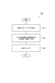
図1は、一つの例示的実施形態に係る基板を処理する方法の流れ図である。図1に示す方法(以下、「方法MT」という)は、有機マスクを有する基板を処理することを含む。図2の(a)は、一例の基板の部分拡大断面図である。図2の(a)に示す基板Wは、有機マスクOMを有する。一実施形態において、基板Wは、膜MF及び下地領域URを更に有し得る。膜MFは、下地領域UR上に設けられている。有機マスクOMは、膜MF上に設けられている。有機マスクOMは、有機材料から形成されており、パターニングされている。有機マスクOMのパターンは、膜MFに転写されるパターンであり得る。有機マスクOMは、例えば、フォトレジストマスクである。有機マスクOMは、例えばフォトリソグラフィ技術により形成され得る。 FIG. 1 is a flow chart of a method for processing a substrate according to one exemplary embodiment. The method shown in FIG. 1 (hereinafter referred to as “method MT”) includes processing a substrate having an organic mask. FIG. 2A is a partially enlarged cross-sectional view of an example substrate. The substrate W shown in FIG. 2A has an organic mask OM. In one embodiment, the substrate W may further have a membrane MF and a substrate region UR. The membrane MF is provided on the base region UR. The organic mask OM is provided on the membrane MF. The organic mask OM is formed from an organic material and is patterned. The pattern of the organic mask OM can be a pattern that is transferred to the membrane MF. The organic mask OM is, for example, a photoresist mask. The organic mask OM can be formed, for example, by a photolithography technique.
膜MFは、単層の膜であってもよい。或いは、膜MFは、図2の(b)に示すように多層膜であってもよい。図2の(b)に示す基板Wにおいて、膜MFは、膜ARF、膜OF、及び膜OXFを含む。膜OXFは、下地領域UR上に設けられている。膜OXFは、例えばシリコン酸化膜である。膜OFは、膜OXF上に設けられている。膜OFは、例えば有機膜である。膜ARFは、膜OF上に設けられている。膜ARFは、例えばシリコンを含有する反射防止膜である。 The membrane MF may be a monolayer membrane. Alternatively, the membrane MF may be a multilayer membrane as shown in FIG. 2 (b). In the substrate W shown in FIG. 2B, the membrane MF includes a membrane ARF, a membrane OF, and a membrane OXF. The film OXF is provided on the base region UR. The film OXF is, for example, a silicon oxide film. The membrane OF is provided on the membrane OXF. The membrane OF is, for example, an organic membrane. The membrane ARF is provided on the membrane OF. The film ARF is, for example, an antireflection film containing silicon.
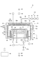
方法MTは、工程ST1及び工程ST2を含む。方法MTの工程ST1及び工程ST2は、基板Wがプラズマ処理装置のチャンバ内に収容された状態で実行される。図3は、一つの例示的実施形態に係るプラズマ処理装置を概略的に示す図である。図3に示すプラズマ処理装置1は、方法MTの実行において用いられ得る。プラズマ処理装置1は、容量結合型プラズマ処理装置である。
Method MT includes step ST1 and step ST2. Steps ST1 and ST2 of the method MT are executed in a state where the substrate W is housed in the chamber of the plasma processing apparatus. FIG. 3 is a diagram schematically showing a plasma processing apparatus according to one exemplary embodiment. The
プラズマ処理装置1は、チャンバ10を備えている。チャンバ10は、その中に内部空間10sを提供している。チャンバ10は、チャンバ本体12を含んでいる。チャンバ本体12は、略円筒形状を有している。内部空間10sは、チャンバ本体12の内側に提供されている。チャンバ本体12は、アルミニウムといった導体から形成されている。チャンバ本体12は、接地されている。チャンバ本体12の内壁面には、耐腐食性を有する膜が施されている。耐腐食性を有する膜は、酸化アルミニウム、酸化イットリウムといったセラミックから形成された膜であり得る。
The
チャンバ本体12の側壁には、通路12pが形成されている。基板Wは、内部空間10sとチャンバ10の外部との間で搬送されるときに、通路12pを通過する。通路12pは、ゲートバルブ12gにより開閉可能となっている。ゲートバルブ12gは、チャンバ本体12の側壁に沿って設けられている。
A
チャンバ本体12の底部上には、支持部13が設けられている。支持部13は、絶縁材料から形成されている。支持部13は、略円筒形状を有している。支持部13は、内部空間10sの中で、チャンバ本体12の底部から上方に延在している。支持部13は、基板支持器14を支持している。基板支持器14は、チャンバ10内、即ち内部空間10sの中で、基板Wを支持するように構成されている。
A
基板支持器14は、下部電極18及び静電チャック20を有している。下部電極18及び静電チャック20は、チャンバ10内に設けられている。基板支持器14は、電極プレート16を更に有し得る。電極プレート16は、例えばアルミニウムといった導体から形成されており、略円盤形状を有している。下部電極18は、電極プレート16上に設けられている。下部電極18は、例えばアルミニウムといった導体から形成されており、略円盤形状を有している。下部電極18は、電極プレート16に電気的に接続されている。
The substrate support 14 has a lower electrode 18 and an
静電チャック20は、下部電極18上に設けられている。静電チャック20の上面の上には、基板Wが載置される。静電チャック20は、本体及び電極を有する。静電チャック20の本体は、誘電体から形成されている。静電チャック20の電極は、膜状の電極であり、静電チャック20の本体内に設けられている。静電チャック20の電極は、スイッチ20sを介して直流電源20pに接続されている。静電チャック20の電極に直流電源20pからの電圧が印加されると、静電チャック20と基板Wとの間で静電引力が発生する。発生した静電引力により、基板Wは、静電チャック20に引き付けられ、静電チャック20によって保持される。
The
基板支持器14上には、エッジリングERが配置される。エッジリングERは、限定されるものではないが、シリコン、炭化シリコン、又は石英から形成され得る。チャンバ10内において基板Wの処理が行われるときには、基板Wは、静電チャック20上、且つ、エッジリングERによって囲まれた領域内に、配置される。
An edge ring ER is arranged on the substrate support 14. The edge ring ER can be formed from, but not limited to, silicon, silicon carbide, or quartz. When the substrate W is processed in the
下部電極18の内部には、流路18fが設けられている。流路18fには、チラーユニット22から配管22aを介して熱交換媒体(例えば冷媒)が供給される。チラーユニット22は、チャンバ10の外部に設けられている。流路18fに供給された熱交換媒体は、配管22bを介してチラーユニット22に戻される。プラズマ処理装置1では、静電チャック20上に載置された基板Wの温度が、熱交換媒体と下部電極18との熱交換により、調整される。
A
プラズマ処理装置1は、ガス供給ライン24を更に備え得る。ガス供給ライン24は、伝熱ガス(例えばHeガス)を、静電チャック20の上面と基板Wの裏面との間に供給する。伝熱ガスは、伝熱ガス供給機構からガス供給ライン24に供給される。
The
プラズマ処理装置1は、上部電極30を更に備えている。上部電極30は、基板支持器14の上方に設けられている。上部電極30は、部材32を介して、チャンバ本体12の上部に支持されている。部材32は、絶縁性を有する材料から形成されている。上部電極30と部材32は、チャンバ本体12の上部開口を閉じている。
The
上部電極30は、天板34及び支持体36を含み得る。天板34の下面は、内部空間10sの側の下面であり、内部空間10sを画成している。天板34は、シリコン含有材料から形成されている。天板34は、例えばシリコン、炭化シリコン、又は酸化シリコンから形成されている。天板34には、複数のガス吐出孔34aが形成されている。複数のガス吐出孔34aは、天板34をその板厚方向に貫通している。
The
支持体36は、天板34を着脱自在に支持する。支持体36は、アルミニウムといった導電性材料から形成される。支持体36の内部には、ガス拡散室36aが設けられている。支持体36には、複数のガス孔36bが形成されている。複数のガス孔36bは、ガス拡散室36aから下方に延びている。複数のガス孔36bは、複数のガス吐出孔34aにそれぞれ連通している。支持体36には、ガス導入口36cが形成されている。ガス導入口36cは、ガス拡散室36aに接続している。ガス導入口36cには、ガス供給管38が接続されている。
The
ガス供給管38には、バルブ群41、流量制御器群42、及びバルブ群43を介して、ガスソース群40が接続されている。ガスソース群40、バルブ群41、流量制御器群42、及びバルブ群43は、ガス供給部GSを構成している。ガスソース群40は、複数のガスソースを含んでいる。バルブ群41及びバルブ群43の各々は、複数の開閉バルブを含んでいる。流量制御器群42は、複数の流量制御器を含んでいる。流量制御器群42の複数の流量制御器の各々は、マスフローコントローラ又は圧力制御式の流量制御器である。ガスソース群40の複数のガスソースの各々は、バルブ群41の対応の開閉バルブ、流量制御器群42の対応の流量制御器、及びバルブ群43の対応の開閉バルブを介して、ガス供給管38に接続されている。
A
プラズマ処理装置1では、チャンバ本体12の内壁面に沿って、シールド46が着脱自在に設けられている。シールド46は、支持部13の外周にも設けられている。シールド46は、チャンバ本体12にプラズマ処理の副生物が付着することを防止する。シールド46は、接地されている。シールド46は、例えば、アルミニウムから形成された部材の表面に耐腐食性を有する膜を形成することにより構成される。耐腐食性を有する膜は、酸化イットリウムといったセラミックから形成された膜であり得る。なお、一実施形態において、シールド46は、チャンバ10の側壁が有する内壁面10wを提供している。内壁面10wは、第1の領域10a及び第2の領域10bを含んでいる。第1の領域10aは、内部空間10sの側方で延在している。第2の領域10bは、内部空間10sの上方且つ上部電極30の側方で延在している。第1の領域10a及び第2の領域10bは、シールド46ではなく、他の一つ以上の部材、例えば、チャンバ本体12によって提供されていてもよい。
In the
支持部13とチャンバ本体12の側壁との間には、バッフルプレート48が設けられている。バッフルプレート48は、例えば、アルミニウムから形成された部材の表面に耐腐食性を有する膜を形成することにより構成される。耐腐食性を有する膜は、酸化イットリウムといったセラミックから形成された膜であり得る。バッフルプレート48には、複数の貫通孔が形成されている。バッフルプレート48の下方、且つ、チャンバ本体12の底部には、排気口12eが設けられている。排気口12eには、排気管52を介して排気装置50が接続されている。排気装置50は、圧力調整弁及びターボ分子ポンプといった真空ポンプを有している。
A
プラズマ処理装置1は、第1の高周波電源62及び第2の高周波電源64を更に備えている。第1の高周波電源62は、第1の高周波電力を発生する電源である。第1の高周波電力は、一例では、プラズマの生成に適した周波数を有する。第1の高周波電力の周波数は、例えば27MHz〜100MHzの範囲内の周波数である。第1の高周波電源62は、整合器66を介して上部電極30に接続されている。整合器66は、第1の高周波電源62の出力インピーダンスと負荷側(上部電極30側)のインピーダンスを整合させるための回路を有している。なお、第1の高周波電源62は、整合器66及び電極プレート16を介して、下部電極18に接続されていてもよい。
The
第2の高周波電源64は、第2の高周波電力を発生する電源である。第2の高周波電力は、第1の高周波電力の周波数よりも低い周波数を有する。第2の高周波電力は、基板Wにイオンを引き込むためのバイアス用の高周波電力として用いられ得る。第2の高周波電力の周波数は、例えば400kHz〜40MHzの範囲内の周波数である。第2の高周波電源64は、整合器68及び電極プレート16を介して下部電極18に接続されている。整合器68は、第2の高周波電源64の出力インピーダンスと負荷側(下部電極18側)のインピーダンスを整合させるための回路を有している。
The second high
プラズマ処理装置1は、直流電源装置70を更に備えている。直流電源装置70は、上部電極30に電気的に接続されている。直流電源装置70は、パルス状の負極性の直流電圧を周期的に発生するように構成されている。図4は、図3に示すプラズマ処理装置の直流電源装置の構成の一例を示す図である。図5は、一つの例示的実施形態に係るプラズマ処理装置における高周波電力及び直流電源装置の出力電圧の一例を示すタイミングチャートである。図4において、横軸は時間を示している。図4において縦軸は、高周波電力(第1の高周波電力及び/又は第2の高周波電力)の供給及び直流電源装置70の出力電圧を示している。図4において、高周波電力が高レベルであることは、高周波電力が供給されていることを表している。図4において、高周波電力が低レベルであることは、高周波電力が供給されていないことを表している。以下、図3と共に、図4及び図5を参照する。
The
一実施形態において、直流電源装置70は、可変直流電源70a及びスイッチングデバイス70bを有する。可変直流電源70aは、負極性の直流電圧を発生するように構成されている。可変直流電源70aが出力する負極性の直流電圧のレベルは、後述する制御部80によって制御され得る。スイッチングデバイス70bは、その導通状態の切り替えにより、可変直流電源70aと上部電極30との間の接続及び遮断を切り替える。スイッチングデバイス70bの導通状態の切り替えは、制御部80によって制御されてもよい。
In one embodiment, the
パルス状の負極性の直流電圧を周期的に出力するために、直流電源装置70の出力電圧は、周期PTにおける第1の期間P1では、負極性の直流電圧である。一実施形態においては、周期PT内の第1の期間P1では、可変直流電源70aと上部電極30を互いに接続するように、スイッチングデバイス70bの導通状態が切り替わる。直流電源装置70の出力電圧は、周期PTにおける残りの第2の期間P2では、ゼロボルトである。一実施形態においては、周期PT内の第2の期間P2では、可変直流電源70aと上部電極30との間の接続を遮断するよう、スイッチングデバイス70bの導通状態が切り替わる。
In order to periodically output the pulsed negative electrode DC voltage, the output voltage of the DC
一実施形態において、周期PTにおいて第1の期間P1が占める割合、即ちデューティ比(小数表現のデューティー比)は、0.2以上、0.5以下である。なお、デューティ比は、周期PT内でパルス状の負極性の直流電圧が直流電源装置70から上部電極30に印加される時間が占める割合である。
In one embodiment, the ratio occupied by the first period P1 in the period PT, that is, the duty ratio (duty ratio in decimal representation) is 0.2 or more and 0.5 or less. The duty ratio is the ratio of the time during which the pulsed negative electrode DC voltage is applied from the DC
一実施形態において、周期PTの逆数である周波数fは、400kHz以上であり得る。一実施形態において、周波数fは、1MHz以下であり得る。周波数fが1MHz以下である場合には、チャンバ10内でのラジカルの生成に対するイオンの挙動の独立性御性が高くなる。
In one embodiment, the frequency f, which is the reciprocal of the period PT, can be 400 kHz or higher. In one embodiment, the frequency f can be 1 MHz or less. When the frequency f is 1 MHz or less, the independence of the ion behavior with respect to the generation of radicals in the
一実施形態では、第1の期間P1において直流電源装置70から上部電極30に印加されるパルス状の負極性の直流電圧の絶対値は、500V以上、1200V以下である。
In one embodiment, the absolute value of the pulsed negative electrode DC voltage applied from the DC
プラズマ処理装置1は、制御部80を更に備えている。制御部80は、プロセッサ、メモリといった記憶部、入力装置、表示装置、信号の入出力インターフェイス等を備えるコンピュータであり得る。制御部80は、プラズマ処理装置1の各部を制御する。制御部80では、オペレータが、プラズマ処理装置1を管理するためにコマンドの入力操作等を入力装置を用いて行うことができる。また、制御部80では、表示装置により、プラズマ処理装置1の可視化された稼働状況を表示することができる。さらに、制御部80の記憶部には、制御プログラム及びレシピデータが格納されている。制御プログラムは、プラズマ処理装置1で各種処理を実行するために、制御部80のプロセッサによって実行される。制御部80のプロセッサが、制御プログラムを実行し、レシピデータに従ってプラズマ処理装置1の各部を制御することにより、方法MTがプラズマ処理装置1で実行される。
The
以下、図1を再び参照して、それがプラズマ処理装置1を用いて実行される場合を例として、方法MTについて説明する。また、制御部80によるプラズマ処理装置1の各部の制御についても説明する。以下の説明では、図6の(a)、図6の(b)、図6の(c)、及び図6の(d)を参照する。図6の(a)、図6の(b)、図6の(c)、及び図6の(d)は、図1に示す方法における各処理後の一例の基板の部分拡大断面図である。
Hereinafter, the method MT will be described with reference to FIG. 1 again, by exemplifying the case where it is executed by using the
方法MTでは、まず、工程ST1が実行される。工程ST1では、基板Wがチャンバ10内に収容された状態で実行される。基板Wは、チャンバ10内で基板支持器14上に載置され、静電チャック20によって保持される。工程ST1では、チャンバ10内で、処理ガスのプラズマが生成される。処理ガスは、ガス供給部GSから供給される。一実施形態において、処理ガスは、アルゴンガス、水素ガス(H2ガス)、及び窒素ガス(N2ガス)のうち少なくとも一つを含む。一例において、処理ガスは、アルゴンガスと水素ガスの混合ガスである。工程ST1では、チャンバ10内で処理ガスからプラズマを生成するために、第1の高周波電力及び/又は第2の高周波電力が供給される。
In the method MT, first, step ST1 is executed. In step ST1, the substrate W is executed in a state of being housed in the
工程ST1の実行のために、制御部80は、処理ガスをチャンバ10内に供給するようにガス供給部GSを制御する。工程ST1の実行のために、制御部80は、チャンバ10内の圧力を指定された圧力に設定するように排気装置50を制御する。工程ST1の実行のために、制御部80は、第1の高周波電力及び/又は第2の高周波電力を供給するように、第1の高周波電源62及び/又は第2の高周波電源64を制御する。
For the execution of step ST1, the
工程ST2は、工程ST1の実行中に実行される。即ち、工程ST2は、工程ST1においてチャンバ10内で処理ガスからプラズマが生成されているときに、実行される。工程ST2は、チャンバ10内のプラズマからのイオンを上部電極30に供給して上部電極30から放出されるシリコン含有物を基板W上に堆積させるために実行される。工程ST2では、直流電源装置70から上部電極30に周期的にパルス状の負極性の直流電圧が印加される。工程ST2の実行のために、制御部80は、上部電極30に周期的にパルス状の負極性の直流電圧を印加するよう、直流電源装置70を制御する。
Step ST2 is executed during execution of step ST1. That is, the step ST2 is executed when plasma is generated from the processing gas in the
一実施形態において、周期PT内でパルス状の負極性の直流電圧が直流電源装置70から上部電極30に印加される時間が占める割合、即ち上述のデューティ比は、0.2以上、0.5以下である。
In one embodiment, the ratio of the time during which the pulsed negative electrode DC voltage is applied from the DC
一実施形態において、周期PTの逆数である周波数fは、400kHz以上であり得る。一実施形態において、周波数fは、1MHz以下であり得る。周波数fが1MHz以下である場合には、チャンバ10内でのラジカルの生成に対するイオンの挙動の独立性御性が高くなる。
In one embodiment, the frequency f, which is the reciprocal of the period PT, can be 400 kHz or higher. In one embodiment, the frequency f can be 1 MHz or less. When the frequency f is 1 MHz or less, the independence of the ion behavior with respect to the generation of radicals in the
一実施形態では、第1の期間P1において直流電源装置70から上部電極30に印加されるパルス状の負極性の直流電圧の絶対値は、500V以上、1200V以下である。
In one embodiment, the absolute value of the pulsed negative electrode DC voltage applied from the DC
工程ST2では、チャンバ10内のプラズマから正イオンが上部電極30に引き付けられて上部電極30の天板34に衝突する。その結果、上部電極30の天板34から、二次電子及びシリコン含有物が放出される。放出された二次電子及びシリコン含有物は、基板Wに供給される。基板Wの有機マスクOMは、二次電子によって改質され得る。また、放出されたシリコン含有物は、図6の(a)に示すように、基板Wの有機マスクOM上に堆積して、膜DPを形成する。
In step ST2, positive ions are attracted from the plasma in the
チャンバ10内のプラズマから上部電極30に衝突するイオンのエネルギーは、上部電極30に印加される電圧の周波数が低いほど、高くなる傾向がある。方法MTでは、チャンバ10内のプラズマから上部電極30に衝突するイオンのエネルギーは、上部電極30にパルス状の負極性の直流電圧が印加される周期PTの逆数である周波数fに依存する。周波数fは、高周波電力の周波数よりも低い周波数に設定され得る。したがって、方法MTでは、上部電極30に高いエネルギーをもったイオンを衝突させることができる。その結果、上部電極30から比較的多量のシリコン含有物を放出させて、基板Wに供給することができる。方法MTによれば、比較的多量のシリコン含有物を基板W上に堆積することができるので、有機マスクOMのパターンの形状バラツキ及び有機マスクOMの縮小を抑制ことが可能である。なお、有機マスクOMのパターンの形状バラツキは、例えば、LWR(Ligh Width Roughness)により評価され得る。
The energy of ions colliding with the
一実施形態において、方法MTは工程ST3を更に含んでいてもよい。工程ST3では、膜MFがエッチングされる。膜MFは、プラズマ処理装置1を用いてエッチングされてもよい。或いは、膜MFは、別のプラズマ処理装置を用いてエッチングされてもよい。以下、図2の(b)に示した膜MFがプラズマ処理装置1を用いてエッチングされる場合を例として、工程ST3について説明する。
In one embodiment, the method MT may further include step ST3. In step ST3, the membrane MF is etched. The membrane MF may be etched using the
まず、膜ARFのプラズマエッチングのために、別の処理ガスのプラズマがチャンバ10内で生成される。膜ARFがシリコンを含有する反射防止膜である場合には、膜ARFのプラズマエッチング用の処理ガスは、フルオロカーボンガスといったフッ素含有ガスを含み得る。膜ARFのプラズマエッチングのために、制御部80は、処理ガスをチャンバ10内に供給するようにガス供給部GSを制御する。膜ARFのプラズマエッチングのために、制御部80は、チャンバ10内の圧力を指定された圧力に設定するように排気装置50を制御する。膜ARFのプラズマエッチングのために、制御部80は、第1の高周波電力及び/又は第2の高周波電力を供給するように、第1の高周波電源62及び/又は第2の高周波電源64を制御する。膜ARFのプラズマエッチングの結果、図6の(b)に示すように、膜DPによりその幅が調整された有機マスクOMのパターンが、膜ARFに転写される。
First, due to plasma etching of the film ARF, a plasma of another processing gas is generated in the
次いで、膜OFのプラズマエッチングのために、更に別の処理ガスのプラズマがチャンバ10内で生成される。膜OFが有機膜である場合には、膜OFのプラズマエッチング用の処理ガスは、水素ガス及び窒素ガスを含み得る。或いは、膜OFのプラズマエッチング用の処理ガスは、酸素含有ガスを含み得る。膜OFのプラズマエッチングのために、制御部80は、処理ガスをチャンバ10内に供給するようにガス供給部GSを制御する。膜OFのプラズマエッチングのために、制御部80は、チャンバ10内の圧力を指定された圧力に設定するように排気装置50を制御する。膜OFのプラズマエッチングのために、制御部80は、第1の高周波電力及び/又は第2の高周波電力を供給するように、第1の高周波電源62及び/又は第2の高周波電源64を制御する。膜OFのプラズマエッチングの結果、図6の(c)に示すように、膜ARFのパターンが、膜OFに転写される。
Then, for plasma etching of the film OF, a plasma of yet another processing gas is generated in the
次いで、膜OXFのプラズマエッチングのために、更に別の処理ガスのプラズマがチャンバ10内で生成される。膜OXFがシリコン酸化膜である場合には、膜OXFのプラズマエッチング用の処理ガスは、フルオロカーボンガスを含み得る。膜OXFのプラズマエッチングのために、制御部80は、処理ガスをチャンバ10内に供給するようにガス供給部GSを制御する。膜OXFのプラズマエッチングのために、制御部80は、チャンバ10内の圧力を指定された圧力に設定するように排気装置50を制御する。膜OXFのプラズマエッチングのために、制御部80は、第1の高周波電力及び/又は第2の高周波電力を供給するように、第1の高周波電源62及び/又は第2の高周波電源64を制御する。膜OXFのプラズマエッチングの結果、図6の(d)に示すように、膜OFのパターンが、膜OXFに転写される。
Then, for plasma etching of the film OXF, a plasma of yet another processing gas is generated in the
以上、種々の例示的実施形態について説明してきたが、上述した例示的実施形態に限定されることなく、様々な省略、置換、及び変更がなされてもよい。また、異なる実施形態における要素を組み合わせて他の実施形態を形成することが可能である。 Although various exemplary embodiments have been described above, various omissions, substitutions, and changes may be made without being limited to the above-mentioned exemplary embodiments. It is also possible to combine elements in different embodiments to form other embodiments.
以下、方法MTの評価のために行った第1の実験及び第2の実験について説明する。第1の実験及び第2の実験では、図2の(b)に示した基板Wと同じ構造のサンプル基板を準備した。サンプル基板において、有機マスクOMはフォトレジストマスクであった。サンプル基板において、膜ARFはシリコンを含有する反射防止膜であった。サンプル基板において、膜OFは有機膜であった。サンプル基板において、膜OXFはシリコン酸化膜であった。サンプル基板の有機マスクOMは、ラインアンドスペースパターンを有していた。サンプル基板の有機マスクOMにおいて、ラインの幅の平均値は41.8nmであり、ラインのLWRは3.3nmであった。第1の実験では、方法MTの工程ST1及び工程ST2をプラズマ処理装置1を用いてサンプル基板に適用した。第1の実験の工程ST2では、上部電極30に印加したパルス状の負極性の直流電圧の絶対値は−900Vであり、当該パルス状の負極性の直流電圧の周波数fは400kHzであり、当該パルス状の負極性の直流電圧のデューティ比は0.5であった。以下に、第1の実験における工程ST1及び工程ST2の条件を示す。
Hereinafter, the first experiment and the second experiment performed for the evaluation of the method MT will be described. In the first experiment and the second experiment, a sample substrate having the same structure as the substrate W shown in FIG. 2B was prepared. In the sample substrate, the organic mask OM was a photoresist mask. In the sample substrate, the film ARF was an antireflection film containing silicon. In the sample substrate, the membrane OF was an organic membrane. In the sample substrate, the film OXF was a silicon oxide film. The organic mask OM of the sample substrate had a line-and-space pattern. In the organic mask OM of the sample substrate, the average value of the width of the line was 41.8 nm, and the LWR of the line was 3.3 nm. In the first experiment, the steps ST1 and ST2 of the method MT were applied to the sample substrate using the
<第1の実験における工程ST1及び工程ST2の条件>
処理時間:10秒
チャンバ10内の圧力:100mTorr(13.33Pa)
第1の高周波電力:60MHz、300W
第2の高周波電力:0W
処理ガス:10sccmのH2ガス及び800sccmのArガス
<Conditions for steps ST1 and ST2 in the first experiment>
Processing time: 10 seconds Pressure in chamber 10: 100 mTorr (13.33 Pa)
First high frequency power: 60MHz, 300W
Second high frequency power: 0W
Processing gas: 10 sccm H 2 gas and 800 sccm Ar gas
第2の実験では、プラズマ処理装置1を用いて第1の実験と同じ条件で処理ガスのプラズマを生成し、上部電極30に−900Vの直流電圧を連続的に印加して、サンプル基板を処理した。
In the second experiment, the
第1の実験及び第2の実験の各々では、その上に堆積したシリコン含有物によってその形状が調整された有機マスクOMのラインの幅の平均値及びLWRを求めた。第1の実験では、ラインの幅の平均値は41.8nmであり、LWRは2.8nmであった。第2の実験では、ラインの幅の平均値は40.6nmであり、LWRは2.7nmであった。第1の実験及び第2の実験の双方において処理後のLWRは、処理前のサンプル基板のLWRよりも小さくなっていた。また、第2の実験では処理後のラインの幅の平均値が処理前のラインの幅の平均値から減少していたが、第1の実験では処理後のラインの幅の平均値は処理前のラインの幅の平均値と同じであった。よって、方法MTによれば、有機マスクのパターンの形状バラツキ及び有機マスクの縮小を抑制することが可能となることが確認された。 In each of the first experiment and the second experiment, the average value and LWR of the line width of the organic mask OM whose shape was adjusted by the silicon content deposited on it were determined. In the first experiment, the average line width was 41.8 nm and the LWR was 2.8 nm. In the second experiment, the average line width was 40.6 nm and the LWR was 2.7 nm. In both the first experiment and the second experiment, the LWR after the treatment was smaller than the LWR of the sample substrate before the treatment. Further, in the second experiment, the average value of the width of the line after the treatment was reduced from the average value of the width of the line before the treatment, but in the first experiment, the average value of the width of the line after the treatment was before the treatment. It was the same as the average value of the width of the line. Therefore, according to the method MT, it was confirmed that it is possible to suppress the shape variation of the pattern of the organic mask and the reduction of the organic mask.
以上の説明から、本開示の種々の実施形態は、説明の目的で本明細書で説明されており、本開示の範囲及び主旨から逸脱することなく種々の変更をなし得ることが、理解されるであろう。したがって、本明細書に開示した種々の実施形態は限定することを意図しておらず、真の範囲と主旨は、添付の特許請求の範囲によって示される。 From the above description, it is understood that the various embodiments of the present disclosure are described herein for purposes of explanation and that various modifications can be made without departing from the scope and gist of the present disclosure. Will. Therefore, the various embodiments disclosed herein are not intended to be limiting, and the true scope and gist is indicated by the appended claims.
1…プラズマ処理装置、10…チャンバ、30…上部電極、70…直流電源装置、W…基板、OM…有機マスク。 1 ... Plasma processing device, 10 ... Chamber, 30 ... Upper electrode, 70 ... DC power supply device, W ... Substrate, OM ... Organic mask.
Claims (8)
プラズマ処理装置のチャンバ内に前記基板が収容された状態で、前記チャンバ内で処理ガスからプラズマを生成する工程と、
プラズマを生成する前記工程の実行中に、前記プラズマからのイオンを前記プラズマ処理装置の上部電極に供給して該上部電極から放出されるシリコン含有物を前記基板上に堆積させるために、前記上部電極に周期的にパルス状の負極性の直流電圧を印加する工程と、
を含む方法。 A method of processing a substrate having a patterned organic mask.
A step of generating plasma from a processing gas in the chamber while the substrate is housed in the chamber of the plasma processing apparatus.
In order to supply ions from the plasma to the upper electrode of the plasma processing apparatus and deposit silicon-containing substances emitted from the upper electrode on the substrate during the execution of the step of generating the plasma, the upper part thereof. The process of periodically applying a pulsed negative electrode DC voltage to the electrodes,
How to include.
前記チャンバ内で別の処理ガスから生成されるプラズマを用いて、前記膜をエッチングする工程を更に含む、
請求項1〜5の何れか一項に記載の方法。 The substrate further comprises a film, and the organic mask is provided on the film.
Further comprising etching the film with plasma generated from another processing gas in the chamber.
The method according to any one of claims 1 to 5.
前記チャンバ内に設けられた基板支持器と、
前記チャンバ内でプラズマを生成するために高周波電力を発生する高周波電源と、
前記基板支持器の上方に設けられた上部電極と、
前記上部電極に接続された直流電源装置と、
前記高周波電源及び前記直流電源装置を制御するように構成された制御部と、
を備え、
前記制御部は、
前記チャンバ内で処理ガスからプラズマを生成するために高周波電力を供給するよう、前記高周波電源を制御し、
前記チャンバ内で前記処理ガスから前記プラズマが生成されているときに、該プラズマからのイオンを前記上部電極に供給して該上部電極から放出されるシリコン含有物を前記基板上に堆積させるために、前記上部電極に周期的にパルス状の負極性の直流電圧を印加するよう、前記直流電源装置を制御する、
プラズマ処理装置。 With the chamber
A substrate support provided in the chamber and
A high-frequency power supply that generates high-frequency power to generate plasma in the chamber,
An upper electrode provided above the substrate support and
A DC power supply connected to the upper electrode and
A control unit configured to control the high-frequency power supply and the DC power supply device, and
With
The control unit
The high frequency power supply is controlled to supply high frequency power to generate plasma from the processing gas in the chamber.
In order to supply ions from the plasma to the upper electrode and deposit silicon-containing substances released from the upper electrode on the substrate when the plasma is generated from the processing gas in the chamber. Control the DC power supply device so as to periodically apply a pulsed negative DC voltage to the upper electrode.
Plasma processing equipment.
Priority Applications (5)
| Application Number | Priority Date | Filing Date | Title |
|---|---|---|---|
| JP2019151441A JP2021034487A (en) | 2019-08-21 | 2019-08-21 | Method for processing substrate, method for manufacturing device, and plasma processing device |
| US16/989,810 US11081351B2 (en) | 2019-08-21 | 2020-08-10 | Method of processing substrate, device manufacturing method, and plasma processing apparatus |
| TW109127026A TW202113968A (en) | 2019-08-21 | 2020-08-10 | Method of processing substrate, device manufacturing method, and plasma processing apparatus |
| CN202010794270.XA CN112420507A (en) | 2019-08-21 | 2020-08-10 | Method for processing substrate, device manufacturing method, and plasma processing apparatus |
| KR1020200100009A KR20210023699A (en) | 2019-08-21 | 2020-08-10 | Method of processing substrate, device manufacturing method, and plasma processing apparatus |
Applications Claiming Priority (1)
| Application Number | Priority Date | Filing Date | Title |
|---|---|---|---|
| JP2019151441A JP2021034487A (en) | 2019-08-21 | 2019-08-21 | Method for processing substrate, method for manufacturing device, and plasma processing device |
Publications (2)
| Publication Number | Publication Date |
|---|---|
| JP2021034487A true JP2021034487A (en) | 2021-03-01 |
| JP2021034487A5 JP2021034487A5 (en) | 2022-06-02 |
Family
ID=74645600
Family Applications (1)
| Application Number | Title | Priority Date | Filing Date |
|---|---|---|---|
| JP2019151441A Pending JP2021034487A (en) | 2019-08-21 | 2019-08-21 | Method for processing substrate, method for manufacturing device, and plasma processing device |
Country Status (5)
| Country | Link |
|---|---|
| US (1) | US11081351B2 (en) |
| JP (1) | JP2021034487A (en) |
| KR (1) | KR20210023699A (en) |
| CN (1) | CN112420507A (en) |
| TW (1) | TW202113968A (en) |
Families Citing this family (1)
| Publication number | Priority date | Publication date | Assignee | Title |
|---|---|---|---|---|
| JP2022187165A (en) * | 2021-06-07 | 2022-12-19 | 株式会社Screenホールディングス | Substrate processing method and substrate processing apparatus |
Citations (3)
| Publication number | Priority date | Publication date | Assignee | Title |
|---|---|---|---|---|
| JP2006270019A (en) * | 2004-06-21 | 2006-10-05 | Tokyo Electron Ltd | Plasma processing system and method, and computer-readable storage medium |
| JP2017098455A (en) * | 2015-11-26 | 2017-06-01 | 東京エレクトロン株式会社 | Etching method |
| JP2017212331A (en) * | 2016-05-25 | 2017-11-30 | 東京エレクトロン株式会社 | Method for processing processed body |
Family Cites Families (6)
| Publication number | Priority date | Publication date | Assignee | Title |
|---|---|---|---|---|
| US7368392B2 (en) * | 2003-07-10 | 2008-05-06 | Applied Materials, Inc. | Method of fabricating a gate structure of a field effect transistor having a metal-containing gate electrode |
| JP5977509B2 (en) * | 2011-12-09 | 2016-08-24 | 東京エレクトロン株式会社 | Plasma processing method and plasma processing apparatus |
| JP2014082228A (en) * | 2012-10-12 | 2014-05-08 | Tokyo Electron Ltd | Plasma etching method |
| JP6035117B2 (en) | 2012-11-09 | 2016-11-30 | 東京エレクトロン株式会社 | Plasma etching method and plasma etching apparatus |
| US9177796B2 (en) * | 2013-05-03 | 2015-11-03 | Applied Materials, Inc. | Optically tuned hardmask for multi-patterning applications |
| JP7045152B2 (en) * | 2017-08-18 | 2022-03-31 | 東京エレクトロン株式会社 | Plasma processing method and plasma processing equipment |
-
2019
- 2019-08-21 JP JP2019151441A patent/JP2021034487A/en active Pending
-
2020
- 2020-08-10 KR KR1020200100009A patent/KR20210023699A/en active Search and Examination
- 2020-08-10 US US16/989,810 patent/US11081351B2/en active Active
- 2020-08-10 CN CN202010794270.XA patent/CN112420507A/en active Pending
- 2020-08-10 TW TW109127026A patent/TW202113968A/en unknown
Patent Citations (3)
| Publication number | Priority date | Publication date | Assignee | Title |
|---|---|---|---|---|
| JP2006270019A (en) * | 2004-06-21 | 2006-10-05 | Tokyo Electron Ltd | Plasma processing system and method, and computer-readable storage medium |
| JP2017098455A (en) * | 2015-11-26 | 2017-06-01 | 東京エレクトロン株式会社 | Etching method |
| JP2017212331A (en) * | 2016-05-25 | 2017-11-30 | 東京エレクトロン株式会社 | Method for processing processed body |
Also Published As
| Publication number | Publication date |
|---|---|
| TW202113968A (en) | 2021-04-01 |
| US20210057212A1 (en) | 2021-02-25 |
| CN112420507A (en) | 2021-02-26 |
| KR20210023699A (en) | 2021-03-04 |
| US11081351B2 (en) | 2021-08-03 |
Similar Documents
| Publication | Publication Date | Title |
|---|---|---|
| KR102356211B1 (en) | Etching method | |
| US20220051904A1 (en) | Etching method | |
| JP6382055B2 (en) | Method for processing an object | |
| TWI743123B (en) | Plasma processing method | |
| JP6504827B2 (en) | Etching method | |
| JP6928548B2 (en) | Etching method | |
| US11251048B2 (en) | Plasma processing method and plasma processing apparatus | |
| JP7158308B2 (en) | Plasma processing apparatus and plasma processing method | |
| JP2021034487A (en) | Method for processing substrate, method for manufacturing device, and plasma processing device | |
| US11721522B2 (en) | Plasma processing method and plasma processing apparatus | |
| JP7308110B2 (en) | METHOD AND PLASMA PROCESSING APPARATUS FOR ETCHING SILICON OXIDE FILM | |
| KR20220058433A (en) | Etching method and plasma processing apparatus | |
| JP2021034503A (en) | Etching method, device manufacturing method and plasma processing device | |
| JP2016111284A (en) | Plasma processing method | |
| JP2022032235A (en) | Etching method and plasma processing device | |
| JP2022074000A (en) | Etching method and plasma processing apparatus | |
| KR20220117149A (en) | Etching method and plasma processing apparatus |
Legal Events
| Date | Code | Title | Description |
|---|---|---|---|
| A521 | Request for written amendment filed |
Free format text: JAPANESE INTERMEDIATE CODE: A523 Effective date: 20220525 |
|
| A621 | Written request for application examination |
Free format text: JAPANESE INTERMEDIATE CODE: A621 Effective date: 20220525 |
|
| A131 | Notification of reasons for refusal |
Free format text: JAPANESE INTERMEDIATE CODE: A131 Effective date: 20230307 |
|
| A977 | Report on retrieval |
Free format text: JAPANESE INTERMEDIATE CODE: A971007 Effective date: 20230308 |
|
| A521 | Request for written amendment filed |
Free format text: JAPANESE INTERMEDIATE CODE: A523 Effective date: 20230420 |
|
| A02 | Decision of refusal |
Free format text: JAPANESE INTERMEDIATE CODE: A02 Effective date: 20230530 |