JP6327970B2 - Method for etching an insulating film - Google Patents
Method for etching an insulating film Download PDFInfo
- Publication number
- JP6327970B2 JP6327970B2 JP2014126520A JP2014126520A JP6327970B2 JP 6327970 B2 JP6327970 B2 JP 6327970B2 JP 2014126520 A JP2014126520 A JP 2014126520A JP 2014126520 A JP2014126520 A JP 2014126520A JP 6327970 B2 JP6327970 B2 JP 6327970B2
- Authority
- JP
- Japan
- Prior art keywords
- frequency power
- period
- insulating film
- gas
- etching
- Prior art date
- Legal status (The legal status is an assumption and is not a legal conclusion. Google has not performed a legal analysis and makes no representation as to the accuracy of the status listed.)
- Active
Links
- 238000000034 method Methods 0.000 title claims description 40
- 238000005530 etching Methods 0.000 title claims description 21
- NBVXSUQYWXRMNV-UHFFFAOYSA-N fluoromethane Chemical compound FC NBVXSUQYWXRMNV-UHFFFAOYSA-N 0.000 claims description 19
- 238000010494 dissociation reaction Methods 0.000 claims description 7
- 230000005593 dissociations Effects 0.000 claims description 7
- 239000007789 gas Substances 0.000 description 54
- 239000010410 layer Substances 0.000 description 23
- 239000003507 refrigerant Substances 0.000 description 11
- 239000011229 interlayer Substances 0.000 description 6
- 239000000463 material Substances 0.000 description 6
- 238000001020 plasma etching Methods 0.000 description 6
- 230000001681 protective effect Effects 0.000 description 6
- 229910052782 aluminium Inorganic materials 0.000 description 4
- XAGFODPZIPBFFR-UHFFFAOYSA-N aluminium Chemical compound [Al] XAGFODPZIPBFFR-UHFFFAOYSA-N 0.000 description 4
- VYPSYNLAJGMNEJ-UHFFFAOYSA-N Silicium dioxide Chemical compound O=[Si]=O VYPSYNLAJGMNEJ-UHFFFAOYSA-N 0.000 description 3
- 230000008021 deposition Effects 0.000 description 3
- 238000010586 diagram Methods 0.000 description 3
- 238000009792 diffusion process Methods 0.000 description 3
- 229910052731 fluorine Inorganic materials 0.000 description 3
- 150000002500 ions Chemical class 0.000 description 3
- 239000000919 ceramic Substances 0.000 description 2
- 239000011248 coating agent Substances 0.000 description 2
- 238000000576 coating method Methods 0.000 description 2
- 229910021420 polycrystalline silicon Inorganic materials 0.000 description 2
- 229910052710 silicon Inorganic materials 0.000 description 2
- 239000010703 silicon Substances 0.000 description 2
- 229910052814 silicon oxide Inorganic materials 0.000 description 2
- WFKWXMTUELFFGS-UHFFFAOYSA-N tungsten Chemical compound [W] WFKWXMTUELFFGS-UHFFFAOYSA-N 0.000 description 2
- 229910052721 tungsten Inorganic materials 0.000 description 2
- 239000010937 tungsten Substances 0.000 description 2
- MYMOFIZGZYHOMD-UHFFFAOYSA-N Dioxygen Chemical compound O=O MYMOFIZGZYHOMD-UHFFFAOYSA-N 0.000 description 1
- PXGOKWXKJXAPGV-UHFFFAOYSA-N Fluorine Chemical compound FF PXGOKWXKJXAPGV-UHFFFAOYSA-N 0.000 description 1
- VRAIHTAYLFXSJJ-UHFFFAOYSA-N alumane Chemical compound [AlH3].[AlH3] VRAIHTAYLFXSJJ-UHFFFAOYSA-N 0.000 description 1
- 229910003481 amorphous carbon Inorganic materials 0.000 description 1
- 239000006227 byproduct Substances 0.000 description 1
- 239000004020 conductor Substances 0.000 description 1
- 239000002826 coolant Substances 0.000 description 1
- 238000001816 cooling Methods 0.000 description 1
- 229910001882 dioxygen Inorganic materials 0.000 description 1
- 239000011737 fluorine Substances 0.000 description 1
- 238000010438 heat treatment Methods 0.000 description 1
- 239000011810 insulating material Substances 0.000 description 1
- 238000004519 manufacturing process Methods 0.000 description 1
- 229910052751 metal Inorganic materials 0.000 description 1
- 239000002184 metal Substances 0.000 description 1
- 238000012986 modification Methods 0.000 description 1
- 230000004048 modification Effects 0.000 description 1
- 229910052756 noble gas Inorganic materials 0.000 description 1
- 230000002093 peripheral effect Effects 0.000 description 1
- 238000009832 plasma treatment Methods 0.000 description 1
- 239000010453 quartz Substances 0.000 description 1
- 239000002356 single layer Substances 0.000 description 1
- XLYOFNOQVPJJNP-UHFFFAOYSA-N water Substances O XLYOFNOQVPJJNP-UHFFFAOYSA-N 0.000 description 1
Images


Classifications
-
- H—ELECTRICITY
- H01—ELECTRIC ELEMENTS
- H01L—SEMICONDUCTOR DEVICES NOT COVERED BY CLASS H10
- H01L21/00—Processes or apparatus adapted for the manufacture or treatment of semiconductor or solid state devices or of parts thereof
- H01L21/02—Manufacture or treatment of semiconductor devices or of parts thereof
- H01L21/04—Manufacture or treatment of semiconductor devices or of parts thereof the devices having at least one potential-jump barrier or surface barrier, e.g. PN junction, depletion layer or carrier concentration layer
- H01L21/18—Manufacture or treatment of semiconductor devices or of parts thereof the devices having at least one potential-jump barrier or surface barrier, e.g. PN junction, depletion layer or carrier concentration layer the devices having semiconductor bodies comprising elements of Group IV of the Periodic System or AIIIBV compounds with or without impurities, e.g. doping materials
- H01L21/30—Treatment of semiconductor bodies using processes or apparatus not provided for in groups H01L21/20 - H01L21/26
- H01L21/31—Treatment of semiconductor bodies using processes or apparatus not provided for in groups H01L21/20 - H01L21/26 to form insulating layers thereon, e.g. for masking or by using photolithographic techniques; After treatment of these layers; Selection of materials for these layers
- H01L21/3105—After-treatment
- H01L21/311—Etching the insulating layers by chemical or physical means
- H01L21/31144—Etching the insulating layers by chemical or physical means using masks
-
- H—ELECTRICITY
- H01—ELECTRIC ELEMENTS
- H01J—ELECTRIC DISCHARGE TUBES OR DISCHARGE LAMPS
- H01J37/00—Discharge tubes with provision for introducing objects or material to be exposed to the discharge, e.g. for the purpose of examination or processing thereof
- H01J37/32—Gas-filled discharge tubes
- H01J37/32009—Arrangements for generation of plasma specially adapted for examination or treatment of objects, e.g. plasma sources
- H01J37/32082—Radio frequency generated discharge
- H01J37/32137—Radio frequency generated discharge controlling of the discharge by modulation of energy
- H01J37/32155—Frequency modulation
- H01J37/32165—Plural frequencies
-
- H—ELECTRICITY
- H01—ELECTRIC ELEMENTS
- H01J—ELECTRIC DISCHARGE TUBES OR DISCHARGE LAMPS
- H01J37/00—Discharge tubes with provision for introducing objects or material to be exposed to the discharge, e.g. for the purpose of examination or processing thereof
- H01J37/32—Gas-filled discharge tubes
- H01J37/32009—Arrangements for generation of plasma specially adapted for examination or treatment of objects, e.g. plasma sources
- H01J37/32082—Radio frequency generated discharge
- H01J37/32137—Radio frequency generated discharge controlling of the discharge by modulation of energy
- H01J37/32146—Amplitude modulation, includes pulsing
-
- H—ELECTRICITY
- H01—ELECTRIC ELEMENTS
- H01J—ELECTRIC DISCHARGE TUBES OR DISCHARGE LAMPS
- H01J37/00—Discharge tubes with provision for introducing objects or material to be exposed to the discharge, e.g. for the purpose of examination or processing thereof
- H01J37/32—Gas-filled discharge tubes
- H01J37/32431—Constructional details of the reactor
- H01J37/3244—Gas supply means
- H01J37/32449—Gas control, e.g. control of the gas flow
-
- H—ELECTRICITY
- H01—ELECTRIC ELEMENTS
- H01L—SEMICONDUCTOR DEVICES NOT COVERED BY CLASS H10
- H01L21/00—Processes or apparatus adapted for the manufacture or treatment of semiconductor or solid state devices or of parts thereof
- H01L21/02—Manufacture or treatment of semiconductor devices or of parts thereof
- H01L21/02104—Forming layers
- H01L21/02107—Forming insulating materials on a substrate
- H01L21/02109—Forming insulating materials on a substrate characterised by the type of layer, e.g. type of material, porous/non-porous, pre-cursors, mixtures or laminates
- H01L21/02112—Forming insulating materials on a substrate characterised by the type of layer, e.g. type of material, porous/non-porous, pre-cursors, mixtures or laminates characterised by the material of the layer
- H01L21/02123—Forming insulating materials on a substrate characterised by the type of layer, e.g. type of material, porous/non-porous, pre-cursors, mixtures or laminates characterised by the material of the layer the material containing silicon
- H01L21/02164—Forming insulating materials on a substrate characterised by the type of layer, e.g. type of material, porous/non-porous, pre-cursors, mixtures or laminates characterised by the material of the layer the material containing silicon the material being a silicon oxide, e.g. SiO2
-
- H—ELECTRICITY
- H01—ELECTRIC ELEMENTS
- H01L—SEMICONDUCTOR DEVICES NOT COVERED BY CLASS H10
- H01L21/00—Processes or apparatus adapted for the manufacture or treatment of semiconductor or solid state devices or of parts thereof
- H01L21/02—Manufacture or treatment of semiconductor devices or of parts thereof
- H01L21/04—Manufacture or treatment of semiconductor devices or of parts thereof the devices having at least one potential-jump barrier or surface barrier, e.g. PN junction, depletion layer or carrier concentration layer
- H01L21/18—Manufacture or treatment of semiconductor devices or of parts thereof the devices having at least one potential-jump barrier or surface barrier, e.g. PN junction, depletion layer or carrier concentration layer the devices having semiconductor bodies comprising elements of Group IV of the Periodic System or AIIIBV compounds with or without impurities, e.g. doping materials
- H01L21/30—Treatment of semiconductor bodies using processes or apparatus not provided for in groups H01L21/20 - H01L21/26
- H01L21/302—Treatment of semiconductor bodies using processes or apparatus not provided for in groups H01L21/20 - H01L21/26 to change their surface-physical characteristics or shape, e.g. etching, polishing, cutting
- H01L21/306—Chemical or electrical treatment, e.g. electrolytic etching
- H01L21/3065—Plasma etching; Reactive-ion etching
- H01L21/30655—Plasma etching; Reactive-ion etching comprising alternated and repeated etching and passivation steps, e.g. Bosch process
-
- H—ELECTRICITY
- H01—ELECTRIC ELEMENTS
- H01L—SEMICONDUCTOR DEVICES NOT COVERED BY CLASS H10
- H01L21/00—Processes or apparatus adapted for the manufacture or treatment of semiconductor or solid state devices or of parts thereof
- H01L21/02—Manufacture or treatment of semiconductor devices or of parts thereof
- H01L21/04—Manufacture or treatment of semiconductor devices or of parts thereof the devices having at least one potential-jump barrier or surface barrier, e.g. PN junction, depletion layer or carrier concentration layer
- H01L21/18—Manufacture or treatment of semiconductor devices or of parts thereof the devices having at least one potential-jump barrier or surface barrier, e.g. PN junction, depletion layer or carrier concentration layer the devices having semiconductor bodies comprising elements of Group IV of the Periodic System or AIIIBV compounds with or without impurities, e.g. doping materials
- H01L21/30—Treatment of semiconductor bodies using processes or apparatus not provided for in groups H01L21/20 - H01L21/26
- H01L21/31—Treatment of semiconductor bodies using processes or apparatus not provided for in groups H01L21/20 - H01L21/26 to form insulating layers thereon, e.g. for masking or by using photolithographic techniques; After treatment of these layers; Selection of materials for these layers
- H01L21/3105—After-treatment
- H01L21/311—Etching the insulating layers by chemical or physical means
- H01L21/31105—Etching inorganic layers
- H01L21/31111—Etching inorganic layers by chemical means
- H01L21/31116—Etching inorganic layers by chemical means by dry-etching
-
- H—ELECTRICITY
- H01—ELECTRIC ELEMENTS
- H01L—SEMICONDUCTOR DEVICES NOT COVERED BY CLASS H10
- H01L21/00—Processes or apparatus adapted for the manufacture or treatment of semiconductor or solid state devices or of parts thereof
- H01L21/02—Manufacture or treatment of semiconductor devices or of parts thereof
- H01L21/04—Manufacture or treatment of semiconductor devices or of parts thereof the devices having at least one potential-jump barrier or surface barrier, e.g. PN junction, depletion layer or carrier concentration layer
- H01L21/18—Manufacture or treatment of semiconductor devices or of parts thereof the devices having at least one potential-jump barrier or surface barrier, e.g. PN junction, depletion layer or carrier concentration layer the devices having semiconductor bodies comprising elements of Group IV of the Periodic System or AIIIBV compounds with or without impurities, e.g. doping materials
- H01L21/30—Treatment of semiconductor bodies using processes or apparatus not provided for in groups H01L21/20 - H01L21/26
- H01L21/31—Treatment of semiconductor bodies using processes or apparatus not provided for in groups H01L21/20 - H01L21/26 to form insulating layers thereon, e.g. for masking or by using photolithographic techniques; After treatment of these layers; Selection of materials for these layers
- H01L21/3205—Deposition of non-insulating-, e.g. conductive- or resistive-, layers on insulating layers; After-treatment of these layers
- H01L21/321—After treatment
- H01L21/3213—Physical or chemical etching of the layers, e.g. to produce a patterned layer from a pre-deposited extensive layer
- H01L21/32133—Physical or chemical etching of the layers, e.g. to produce a patterned layer from a pre-deposited extensive layer by chemical means only
- H01L21/32135—Physical or chemical etching of the layers, e.g. to produce a patterned layer from a pre-deposited extensive layer by chemical means only by vapour etching only
- H01L21/32136—Physical or chemical etching of the layers, e.g. to produce a patterned layer from a pre-deposited extensive layer by chemical means only by vapour etching only using plasmas
- H01L21/32137—Physical or chemical etching of the layers, e.g. to produce a patterned layer from a pre-deposited extensive layer by chemical means only by vapour etching only using plasmas of silicon-containing layers
-
- H—ELECTRICITY
- H01—ELECTRIC ELEMENTS
- H01L—SEMICONDUCTOR DEVICES NOT COVERED BY CLASS H10
- H01L21/00—Processes or apparatus adapted for the manufacture or treatment of semiconductor or solid state devices or of parts thereof
- H01L21/67—Apparatus specially adapted for handling semiconductor or electric solid state devices during manufacture or treatment thereof; Apparatus specially adapted for handling wafers during manufacture or treatment of semiconductor or electric solid state devices or components ; Apparatus not specifically provided for elsewhere
- H01L21/67005—Apparatus not specifically provided for elsewhere
- H01L21/67011—Apparatus for manufacture or treatment
- H01L21/67017—Apparatus for fluid treatment
- H01L21/67063—Apparatus for fluid treatment for etching
- H01L21/67069—Apparatus for fluid treatment for etching for drying etching
-
- H—ELECTRICITY
- H01—ELECTRIC ELEMENTS
- H01L—SEMICONDUCTOR DEVICES NOT COVERED BY CLASS H10
- H01L21/00—Processes or apparatus adapted for the manufacture or treatment of semiconductor or solid state devices or of parts thereof
- H01L21/70—Manufacture or treatment of devices consisting of a plurality of solid state components formed in or on a common substrate or of parts thereof; Manufacture of integrated circuit devices or of parts thereof
- H01L21/71—Manufacture of specific parts of devices defined in group H01L21/70
- H01L21/768—Applying interconnections to be used for carrying current between separate components within a device comprising conductors and dielectrics
- H01L21/76801—Applying interconnections to be used for carrying current between separate components within a device comprising conductors and dielectrics characterised by the formation and the after-treatment of the dielectrics, e.g. smoothing
- H01L21/76802—Applying interconnections to be used for carrying current between separate components within a device comprising conductors and dielectrics characterised by the formation and the after-treatment of the dielectrics, e.g. smoothing by forming openings in dielectrics
-
- H—ELECTRICITY
- H01—ELECTRIC ELEMENTS
- H01J—ELECTRIC DISCHARGE TUBES OR DISCHARGE LAMPS
- H01J2237/00—Discharge tubes exposing object to beam, e.g. for analysis treatment, etching, imaging
- H01J2237/32—Processing objects by plasma generation
- H01J2237/33—Processing objects by plasma generation characterised by the type of processing
- H01J2237/334—Etching
Description
本発明の実施形態は、絶縁膜をエッチングする方法に関するものである。 Embodiments described herein relate generally to a method for etching an insulating film.
電子デバイスの製造においては、層間絶縁膜にコンタクト用の開口が形成されることがある。この層間絶縁膜を有する被処理体では、層間絶縁膜は配線層上に形成され、当該層間絶縁膜層上には、開口形成のための有機膜からなるマスクが設けられる。このような被処理体の絶縁膜に開口を形成するためには、一般的には、プラズマエッチングが用いられる。 In the manufacture of an electronic device, a contact opening may be formed in an interlayer insulating film. In the object having the interlayer insulating film, the interlayer insulating film is formed on the wiring layer, and a mask made of an organic film for forming an opening is provided on the interlayer insulating film layer. In order to form an opening in such an insulating film of the object to be processed, plasma etching is generally used.
層間絶縁膜のプラズマエッチングでは、プラズマ処理装置の処理容器内においてフルオロカーボンを含む処理ガスが励起される。これにより生成される活性種によって、絶縁膜がエッチングされる。 In plasma etching of an interlayer insulating film, a processing gas containing fluorocarbon is excited in a processing container of a plasma processing apparatus. The insulating film is etched by the active species generated thereby.
下記の特許文献1には、このようなプラズマエッチングが開示されている。特許文献1に記載されたプラズマエッチングでは、処理ガスを励起させるための高周波電力がONとOFFに周期的に切り換えられている。 Patent Document 1 below discloses such plasma etching. In plasma etching described in Patent Document 1, high-frequency power for exciting a processing gas is periodically switched between ON and OFF.
ところで、絶縁膜のエッチングには、マスク及び配線層のエッチングを抑制すること、即ち、選択性を有することが求められる。しかしながら、従来のプラズマエッチングでは、絶縁膜のエッチングに対して、マスク及び配線層のエッチングを十分に抑制することができない。 By the way, the etching of the insulating film is required to suppress the etching of the mask and the wiring layer, that is, to have selectivity. However, the conventional plasma etching cannot sufficiently suppress the etching of the mask and the wiring layer as compared with the etching of the insulating film.
したがって、マスク及び配線層に対して絶縁膜を選択的にエッチングすることが必要となっている。 Therefore, it is necessary to selectively etch the insulating film with respect to the mask and the wiring layer.
一側面においては、被処理体の絶縁膜をエッチングする方法が提供される。被処理体は、配線層、該配線層上に設けられた絶縁膜、及び該絶縁膜上に設けられた有機膜から構成されたマスクを有している。この方法は、(a)第1の期間内において、プラズマ処理装置の処理容器内に供給されたフルオロカーボンを含む処理ガスを励起させるために、高周波電力のONとOFFを周期的に切り換える工程(以下、「第1工程」という)と、(b)第1の期間に続く第2の期間であり、第1の期間内において高周波電力がONとなる期間と高周波電力がOFFとなる期間からなる一周期内において高周波電力がONとなる期間よりも長い該第2の期間内において、処理容器内に供給された処理ガスを励起させるために、高周波電力を連続的にONに設定する工程(以下、「第2工程」という)と、を含む。この方法では、第1工程と第2工程とが交互に繰り返される。一実施形態では、絶縁膜は酸化シリコン製であり、配線層は多結晶シリコン製又はタングステン製である。 In one aspect, a method for etching an insulating film of an object to be processed is provided. The object to be processed has a mask composed of a wiring layer, an insulating film provided on the wiring layer, and an organic film provided on the insulating film. In this method, (a) a step of periodically switching ON and OFF of high-frequency power in order to excite a processing gas containing a fluorocarbon supplied into a processing container of a plasma processing apparatus within a first period (hereinafter referred to as a process). , "First step") and (b) a second period following the first period, which is composed of a period in which the high-frequency power is turned on and a period in which the high-frequency power is turned off in the first period. In the second period longer than the period in which the high-frequency power is turned on in the cycle, the step of continuously setting the high-frequency power to ON in order to excite the processing gas supplied into the processing container (hereinafter, (Referred to as “second step”). In this method, the first step and the second step are alternately repeated. In one embodiment, the insulating film is made of silicon oxide, and the wiring layer is made of polycrystalline silicon or tungsten.
この方法の第1の期間では、高周波電力のONとOFFとが周期的に切り換えられる。第1の期間における高周波電力の供給、即ち、ONとOFFとが交互に切り替わる高周波電力の供給により、フルオロカーボンから、低次の活性種よりも高次の活性種が主として生成される。高次の活性種はマスク表面に付着し易く、絶縁膜のエッチング中にマスクを保護する保護膜を形成する。また、高次の活性種は、形成される開口の深部には到達し難く、従って、配線層を保護する膜を形成することができない。 In the first period of this method, the high-frequency power is periodically switched on and off. By supplying high-frequency power in the first period, that is, by supplying high-frequency power that switches between ON and OFF alternately, higher-order active species than low-order active species are mainly generated from the fluorocarbon. Higher-order active species easily adhere to the mask surface, and form a protective film that protects the mask during etching of the insulating film. In addition, higher-order active species cannot easily reach the deep portion of the opening to be formed, and therefore, a film that protects the wiring layer cannot be formed.
一方、第2期間では、高周波電力が連続的にONに設定される。第2の期間の高周波電力の供給、即ち連続的にON状態を維持する高周波電力の供給により、フルオロカーボンから、高次の活性種よりも低次の活性種が主として生成される。即ち、第2の期間の高周波電力の供給により、第1の期間の高周波電力の供給によるよりも、フルオロカーボンの解離度が高くなる。低次の活性種は、マスクを多くエッチングし得るが、開口の深部まで到達して配線層上に保護膜を形成することができる。したがって、第1工程と第2工程を交互に繰り返して実行することにより、絶縁膜のエッチング中にマスク及び配線層を保護することが可能となる。故に、この方法によれば、マスク及び配線層に対して絶縁膜を選択的にエッチングすることが可能となる。 On the other hand, in the second period, the high frequency power is continuously set to ON. By supplying the high-frequency power in the second period, that is, by supplying the high-frequency power that keeps the ON state continuously, active species of lower order than high-order active species are mainly generated from the fluorocarbon. That is, the supply of high-frequency power in the second period increases the degree of dissociation of the fluorocarbon as compared to the supply of high-frequency power in the first period. The low-order active species can etch a large amount of the mask, but can reach the deep portion of the opening and form a protective film on the wiring layer. Accordingly, by alternately repeating the first step and the second step, it is possible to protect the mask and the wiring layer during the etching of the insulating film. Therefore, according to this method, the insulating film can be selectively etched with respect to the mask and the wiring layer.
一実施形態では、絶縁膜は、単一の膜であってもよい。また、一実施形態では、第2の期間は、一周期内において高周波電力がONとなる期間より100倍以上長い期間であり得る。 In one embodiment, the insulating film may be a single film. In one embodiment, the second period may be a period 100 times longer than the period in which the high-frequency power is turned on in one cycle.
以上説明したように、マスク及び配線層に対して絶縁膜を選択的にエッチングすることが可能となる。 As described above, the insulating film can be selectively etched with respect to the mask and the wiring layer.
以下、図面を参照して種々の実施形態について詳細に説明する。なお、各図面において同一又は相当の部分に対しては同一の符号を附すこととする。 Hereinafter, various embodiments will be described in detail with reference to the drawings. In the drawings, the same or corresponding parts are denoted by the same reference numerals.
図1は、一実施形態に係る絶縁膜をエッチングする方法を示す流れ図である。図1に示す方法MTは、被処理体(以下、「ウエハW」という)の絶縁膜をエッチングする方法であり、交互に繰り返される工程S1及び工程S2を含んでいる。 FIG. 1 is a flowchart illustrating a method for etching an insulating film according to an embodiment. A method MT shown in FIG. 1 is a method of etching an insulating film of an object to be processed (hereinafter referred to as “wafer W”), and includes steps S1 and S2 that are alternately repeated.
図2は、被処理体の一例を示す図である。方法MTは、例えば、図2に示すウエハWに対して適用され得る。このウエハWは、配線層102、絶縁膜104、及びマスク106を有している。配線層102は、例えば、多結晶シリコン、又はタングステンから構成されている。
FIG. 2 is a diagram illustrating an example of an object to be processed. The method MT can be applied to, for example, the wafer W shown in FIG. This wafer W has a
絶縁膜104は、配線層102上に設けられている。一実施形態では、絶縁膜104は単一の絶縁膜、即ち単層である。また、一実施形態では、絶縁膜104は、層間絶縁膜であり、例えば、酸化シリコンから構成されている。絶縁膜104は、フルオロカーボンガスのプラズマを用いることにより配線層102及びマスク106に対して選択的にエッチングされる絶縁膜であれば、任意の材料から構成され得る。マスク106は、絶縁膜104上に設けられている。マスク106は、有機膜から構成されている。例えば、マスク106は、アモルファスカーボン、又はレジスト材料から構成されている。マスク106には、絶縁膜104に転写されるべきパターンが形成されている。即ち、マスク106には、開口が形成されている。
The
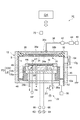
方法MTの実施には、図3に示すプラズマ処理装置を用いることができる。図3は、一実施形態に係るプラズマ処理装置を概略的に示す図である。図3に示すように、プラズマ処理装置10は、容量結合型プラズマエッチング装置であり、処理容器12を備えている。処理容器12は、略円筒形状を有している。処理容器12は、例えば、アルミニウムから構成されており、その内壁面には陽極酸化処理が施されている。この処理容器12は保安接地されている。
The plasma processing apparatus shown in FIG. 3 can be used for performing the method MT. FIG. 3 is a diagram schematically illustrating a plasma processing apparatus according to an embodiment. As shown in FIG. 3, the
処理容器12の底部上には、略円筒状の支持部14が設けられている。支持部14は、例えば、絶縁材料から構成されている。支持部14は、処理容器12内において、処理容器12の底部から鉛直方向に延在している。また、処理容器12内には、載置台PDが設けられている。載置台PDは、支持部14によって支持されている。
A substantially
載置台PDは、その上面においてウエハWを保持する。載置台PDは、下部電極LE及び静電チャックESCを有している。下部電極LEは、第1プレート18a及び第2プレート18bを含んでいる。第1プレート18a及び第2プレート18bは、例えばアルミアルミニウムといった金属から構成されており、略円盤形状をなしている。第2プレート18bは、第1プレート18a上に設けられており、第1プレート18aに電気的に接続されている。
The mounting table PD holds the wafer W on the upper surface thereof. The mounting table PD includes a lower electrode LE and an electrostatic chuck ESC. The lower electrode LE includes a
第2プレート18b上には、静電チャックESCが設けられている。静電チャックESCは、導電膜である電極を一対の絶縁層又は絶縁シート間に配置した構造を有している。静電チャックESCの電極には、直流電源22がスイッチ23を介して電気的に接続されている。この静電チャックESCは、直流電源22からの直流電圧により生じたクーロン力等の静電力によりウエハWを吸着する。これにより、静電チャックESCは、ウエハWを保持することができる。
An electrostatic chuck ESC is provided on the
第2プレート18bの周縁部上には、ウエハWのエッジ及び静電チャックESCを囲むようにフォーカスリングFRが配置されている。フォーカスリングFRは、エッチングの均一性を向上させるために設けられている。フォーカスリングFRは、エッチング対象の膜の材料によって適宜選択される材料から構成されており、例えば、石英から構成され得る。
A focus ring FR is disposed on the peripheral edge of the
第2プレート18bの内部には、冷媒流路24が設けられている。冷媒流路24は、温調機構を構成している。冷媒流路24には、処理容器12の外部に設けられたチラーユニットから配管26aを介して冷媒が供給される。冷媒流路24に供給された冷媒は、配管26bを介してチラーユニットに戻される。このように、冷媒流路24には、冷媒が循環するよう、供給される。この冷媒の温度を制御することにより、静電チャックESCによって支持されたウエハWの温度が制御される。
A
また、プラズマ処理装置10には、ガス供給ライン28が設けられている。ガス供給ライン28は、伝熱ガス供給機構からの伝熱ガス、例えばHeガスを、静電チャックESCの上面とウエハWの裏面との間に供給する。
The
また、プラズマ処理装置10には、加熱素子であるヒータHTが設けられている。ヒータHTは、例えば、第2プレート18b内に埋め込まれている。ヒータHTには、ヒータ電源HPが接続されている。ヒータ電源HPからヒータHTに電力が供給されることにより、載置台PDの温度が調整され、当該載置台PD上に載置されるウエハWの温度が調整されるようになっている。なお、ヒータHTは、静電チャックESCに内蔵されていてもよい。
Further, the
また、プラズマ処理装置10は、上部電極30を備えている。上部電極30は、載置台PDの上方において、当該載置台PDと対向配置されている。下部電極LEと上部電極30とは、互いに略平行に設けられている。これら上部電極30と下部電極LEとの間には、ウエハWにプラズマ処理を行うための処理空間Sが提供されている。
In addition, the
上部電極30は、絶縁性遮蔽部材32を介して、処理容器12の上部に支持されている。一実施形態では、上部電極30は、載置台PDの上面、即ち、ウエハ載置面からの鉛直方向における距離が可変であるように構成され得る。上部電極30は、電極板34及び電極支持体36を含み得る。電極板34は処理空間Sに面しており、当該電極板34には複数のガス吐出孔34aが設けられている。この電極板34は、一実施形態では、シリコンから構成されている。
The
電極支持体36は、電極板34を着脱自在に支持するものであり、例えばアルミニウムといった導電性材料から構成され得る。この電極支持体36は、水冷構造を有し得る。電極支持体36の内部には、ガス拡散室36aが設けられている。このガス拡散室36aからは、ガス吐出孔34aに連通する複数のガス通流孔36bが下方に延びている。また、電極支持体36には、ガス拡散室36aに処理ガスを導くガス導入口36cが形成されており、このガス導入口36cには、ガス供給管38が接続されている。
The
ガス供給管38には、バルブ群42及び流量制御器群44を介して、ガスソース群40が接続されている。ガスソース群40は、複数のガスソースを有している。複数のガスソースは、一以上のフルオロカーボンガスのソース、酸素ガス(O2ガス)のソース、及び、希ガスのソースを含み得る。フルオロカーボンガスは、C4F6、C4F8、及びC6F6のうち少なくとも一種を含むガスであり得る。一実施形態では、複数のガスソースは、C4F6ガスのソース、及びC4F8ガスのソースを含み得る。また、希ガスは、Arガス、Heガスといった任意の希ガスのソースであることができる。
A
バルブ群42は複数のバルブを含んでおり、流量制御器群44はマスフローコントローラといった複数の流量制御器を含んでいる。ガスソース群40の複数のガスソースはそれぞれ、バルブ群42の対応のバルブ及び流量制御器群44の対応の流量制御器を介して、ガス供給管38に接続されている。
The
また、プラズマ処理装置10では、処理容器12の内壁に沿ってデポシールド46が着脱自在に設けられている。デポシールド46は、支持部14の外周にも設けられている。デポシールド46は、処理容器12にエッチング副生物(デポ)が付着することを防止するものであり、アルミニウム材にY2O3等のセラミックスを被覆することにより構成され得る。
In the
処理容器12の底部側、且つ、支持部14と処理容器12の側壁との間には排気プレート48が設けられている。排気プレート48は、例えば、アルミニウム材にY2O3等のセラミックスを被覆することにより構成され得る。この排気プレート48の下方、且つ、処理容器12には、排気口12eが設けられている。排気口12eには、排気管52を介して排気装置50が接続されている。排気装置50は、ターボ分子ポンプなどの真空ポンプを有しており、処理容器12内の空間を所望の真空度まで減圧することができる。また、処理容器12の側壁にはウエハWの搬入出口12gが設けられており、この搬入出口12gはゲートバルブ54により開閉可能となっている。
An
また、プラズマ処理装置10は、第1の高周波電源62及び第2の高周波電源64を更に備えている。第1の高周波電源62は、プラズマ生成用の第1の高周波電力を発生する電源であり、27〜100MHzの周波数、一例においては40MHzの高周波電力を発生する。第1の高周波電源62は、整合器66を介して下部電極LEに接続されている。整合器66は、第1の高周波電源62の出力インピーダンスと負荷側(下部電極LE側)の入力インピーダンスを整合させるための回路である。
The
第2の高周波電源64は、ウエハWにイオンを引き込むための第2の高周波電力、即ち高周波バイアス電力を発生する電源であり、400kHz〜13.56MHzの範囲内の周波数、一例においては3.2MHzの高周波バイアス電力を発生する。第2の高周波電源64は、整合器68を介して下部電極LEに接続されている。整合器68は、第2の高周波電源64の出力インピーダンスと負荷側(下部電極LE側)の入力インピーダンスを整合させるための回路である。
The second high-
また、プラズマ処理装置10は、電源70を更に備えている。電源70は、上部電極30に接続されている。電源70は、処理空間S内に存在する正イオンを電極板34に引き込むための電圧を、上部電極30に印加する。一例においては、電源70は、負の直流電圧を発生する直流電源である。別の一例において、電源70は、比較的低周波の交流電圧を発生する交流電源であってもよい。電源70から上部電極に印加される電圧は、−150V以下の電圧であり得る。即ち、電源70によって上部電極30に印加される電圧は、絶対値が150V以上の負の電圧であり得る。このような電圧が電源70から上部電極30に印加されると、処理空間Sに存在する正イオンが、電極板34に衝突する。これにより、電極板34から二次電子及び/又はシリコンが放出される。
The
また、一実施形態においては、プラズマ処理装置10は、制御部Cntを更に備え得る。この制御部Cntは、プロセッサ、記憶部、入力装置、表示装置等を備えるコンピュータであり、プラズマ処理装置10の各部を制御する。具体的に、制御部Cntは、バルブ群42、流量制御器群44、排気装置50、第1の高周波電源62、整合器66、第2の高周波電源64、整合器68、電源70、ヒータ電源HP、及びチラーユニットに接続されている。
In one embodiment, the
制御部Cntは、入力されたレシピに基づくプログラムに従って動作し、制御信号を送出する。制御部Cntからの制御信号により、ガスソース群から供給されるガスの選択及び流量、排気装置50の排気、第1の高周波電源62及び第2の高周波電源64からの電力供給、電源70からの電圧印加、ヒータ電源HPの電力供給、チラーユニットからの冷媒流量及び冷媒温度を制御することが可能である。
The control unit Cnt operates according to a program based on the input recipe and sends out a control signal. In accordance with a control signal from the control unit Cnt, selection and flow rate of gas supplied from the gas source group, exhaust of the
再び図1を参照し、制御部Cntの各種制御と共に、方法MTの各工程について詳細に説明する。また、ここでは、図1に加えて、図4及び図5を参照する。図4は、方法MTの各工程における一例の被処理体の状態を示す断面図である。図5は、方法MTの各工程における高周波電力及び高周波バイアス電力の波形を示す図である。 With reference to FIG. 1 again, each step of the method MT will be described in detail along with various controls of the control unit Cnt. Here, in addition to FIG. 1, FIG. 4 and FIG. 5 are referred to. FIG. 4 is a cross-sectional view showing a state of the object to be processed in each step of the method MT. FIG. 5 is a diagram showing waveforms of the high frequency power and the high frequency bias power in each step of the method MT.
方法MTの工程S1では、処理容器12内にフルオロカーボンガスを含む処理ガスが供給される。処理ガスは、例えば、C4F6ガス、C4F8ガス、O2ガス、及びArガスを含み得る。また、方法MTでは、工程S1が実行される第1の期間T1内において、第1の高周波電源62から供給される高周波電力HFのONとOFFとが周期的に切り換えられる。即ち、第1の期間T1内において、高周波電力HFがパルス状に供給される。高周波電力HFのONとOFFの切り換えの周波数は、0.1kHz〜100kHzの範囲内の周波数である。例えば、この周波数は10kHzである。また、当該周波数によって規定される一周期内において高周波電力HFがONとなる期間T3が占める割合、即ち、デューティー比は、5%〜95%の範囲内の比である。例えば、デューティー比は50%である。
In step S1 of the method MT, a processing gas containing a fluorocarbon gas is supplied into the
一実施形態の工程S1では、高周波電力HFにON/OFFに同期して、第2の高周波電源64から供給される高周波バイアス電力LFのONとOFFとが周期的に切り換えられてもよい。即ち、第1の期間T1内において、高周波バイアス電力LFがパルス状に供給されてもよい。
In step S <b> 1 of one embodiment, the high frequency bias power LF supplied from the second high
この工程S1では、パルス状に供給される高周波電力HFにより、処理ガスが励起される。パルス状に供給される高周波電力HFに基づき生成されるプラズマ中では、フルオロカーボンは、F、CF、CF2といった低次の活性種よりも高次の活性種が多くなるように解離する。換言すると、工程S1ではフルオロカーボンの解離度が、後述する工程S2のフルオロカーボンの解離度よりも低くなる。 In this step S1, the processing gas is excited by the high frequency power HF supplied in a pulse shape. In the plasma generated based on the high-frequency power HF supplied in a pulsed manner, the fluorocarbon dissociates so that higher-order active species such as F, CF, and CF 2 become higher in number. In other words, in step S1, the degree of dissociation of the fluorocarbon is lower than the degree of dissociation of the fluorocarbon in step S2, which will be described later.
図4の(a)に示すように、高次の活性種は、マスク106の表面に付着し易く、フッ素或いはフルオロカーボンの活性種による絶縁膜104のエッチング中に、マスク106を保護する保護膜108を当該マスク106の表面上に形成する。なお、高次の活性種は、エッチングによって形成される開口OPの深部には到達し難い特性を有する。
As shown in FIG. 4A, the higher-order active species easily adhere to the surface of the
この工程S1をプラズマ処理装置10を用いて実行する場合には、制御部Cntは、処理容器12内に上記処理ガスが、設定された流量で供給されるよう、バルブ群42及び流量制御器群44を制御する。また、制御部Cntは、処理空間Sの圧力が設定された圧力となるよう、排気装置50を制御する。また、制御部Cntは、高周波電力HF及び高周波バイアス電力LFがパルス状に供給されるよう、第1の高周波電源62及び第2の高周波電源64を制御する。
When this step S1 is performed using the
なお、高周波電力HFがOFFになっている期間中に電源70からの電圧が上部電極30に印加されるよう、制御部Cntは、電源70を制御してもよい。電源70から上部電極30に電圧が印加されると、電極板34から放出される二次電子によってマスク106が改質される。これにより、マスク106の耐プラズマ性を向上させることができる。また、ウエハWの帯電を中和することが可能となる。これにより、エッチングレート或いはエッチングの直進性を向上させることが可能である。
Note that the control unit Cnt may control the
方法MTでは、続く工程S2においても、処理容器12内に工程S1と同様の処理ガスが供給される。また、方法MTでは、工程S2が実行される第2の期間T2内において、第1の高周波電源62から供給される高周波電力HFが連続的にONに設定される。即ち、第2の期間T2中は、連続的に高周波電力HFが供給される。第2の期間T2は、一実施形態では、期間T3の100倍以上の時間長を有する。例えば、第2の期間T2は、5秒〜100秒の範囲内の時間長に設定され得る。また、一実施形態の工程S2では、高周波電力HFと同様に、第2の高周波電源64から供給される高周波バイアス電力LFも連続的に供給され得る。
In the method MT, the same processing gas as in step S1 is supplied into the
この工程S2では、連続的に供給される高周波電力HFにより、処理ガスが励起される。連続的に供給される高周波電力HFに基づき生成されるプラズマ中では、フルオロカーボンは、高次の活性種よりも、F、CF、CF2といった低次の活性種が多くなるように解離する。換言すると、工程S2ではフルオロカーボンの解離度が、工程S1のフルオロカーボンの解離度よりも高くなる。 In this step S2, the processing gas is excited by the high-frequency power HF that is continuously supplied. In the plasma generated based on the continuously supplied high-frequency power HF, the fluorocarbon dissociates so that there are more low-order active species such as F, CF, and CF 2 than the high-order active species. In other words, in step S2, the degree of dissociation of the fluorocarbon is higher than the degree of dissociation of the fluorocarbon in step S1.
図4の(b)に示すように、低次の活性種は、マスク106を多くエッチングし得るが、開口OPの深部まで到達して配線層102上に保護膜110を形成することができる。したがって、工程S2によれば、配線層102のエッチングを抑制することができる。
As shown in FIG. 4B, the low-order active species can etch the
この工程S2をプラズマ処理装置10を用いて実行する場合には、制御部Cntは、処理容器12内に上記処理ガスが、設定された流量で供給されるよう、バルブ群42及び流量制御器群44を制御する。また、制御部Cntは、処理空間Sの圧力が設定された圧力となるよう、排気装置50を制御する。また、制御部Cntは、高周波電力HF及び高周波バイアス電力LFが連続的に供給されるよう、第1の高周波電源62及び第2の高周波電源64を制御する。なお、第2の期間T2中において電源70からの電圧が上部電極30に印加されるよう、制御部Cntは、電源70を制御してもよい。
When this step S2 is performed using the
方法MTでは、続く工程S3において、停止条件が満たされるか否かが判定される。停止条件は、例えば、工程S1及び工程S2を含むシーケンスの実行回数が所定回数に達したときに満たされる。例えば、所定回数は10回である。工程S3の判定結果がNoである場合には、工程S1及び工程S2の実行が再び繰り返される。一方、工程S3の判定結果がYESである場合には方法MTのプロセスが終了する。 In the method MT, it is determined in the subsequent step S3 whether or not the stop condition is satisfied. The stop condition is satisfied, for example, when the number of execution times of the sequence including the step S1 and the step S2 reaches a predetermined number. For example, the predetermined number is 10 times. When the determination result of step S3 is No, the execution of step S1 and step S2 is repeated again. On the other hand, when the determination result in step S3 is YES, the process of the method MT ends.
以上説明した方法MTによれば、工程S1と工程S2を交互に繰り返して実行することにより、絶縁膜104のエッチング中にマスク106及び配線層102の双方の上に保護膜を形成することが可能となる。故に、この方法MTによれば、マスク106及び配線層102に対して絶縁膜104を選択的にエッチングすることが可能となる。
According to the method MT described above, it is possible to form a protective film on both the
以上、種々の実施形態について説明してきたが、上述した実施形態に限定されることなく種々の変形態様を構成可能である。例えば、第1の高周波電源62は、整合器66を介して上部電極30に接続されていてもよい。
Although various embodiments have been described above, various modifications can be made without being limited to the above-described embodiments. For example, the first high
10…プラズマ処理装置、12…処理容器、PD…載置台、ESC…静電チャック、LE…下部電極、30…上部電極、34…電極板、40…ガスソース群、42…バルブ群、44…流量制御器群、50…排気装置、62…第1の高周波電源、64…第2の高周波電源、70…電源、Cnt…制御部、W…ウエハ、102…配線層、104…絶縁膜、106…マスク、108,110…保護膜。
DESCRIPTION OF
Claims (5)
第1の期間内において、プラズマ処理装置の処理容器内に供給されたフルオロカーボンを含む処理ガスを励起させるために、高周波電力のONとOFFを周期的に切り換える工程と、
前記第1の期間に続く第2の期間であり、前記第1の期間内において前記高周波電力がONとなる期間と前記高周波電力がOFFとなる期間からなる一周期内において前記高周波電力がONとなる該期間よりも長い該第2の期間内において、前記処理容器内に供給された前記処理ガスを励起させるために、高周波電力を連続的にONに設定する工程と、
を含み、
前記高周波電力のONとOFFを周期的に切り換える前記工程と前記高周波電力を連続的にONに設定する前記工程とが交互に繰り返される、方法。 A method for etching an insulating film of an object to be processed, wherein the object to be processed includes a wiring layer, the insulating film provided on the wiring layer, and an organic film provided on the insulating film. Having a mask, the method comprising:
In the first period, in order to excite the processing gas containing the fluorocarbon supplied into the processing container of the plasma processing apparatus, periodically switching ON and OFF of the high-frequency power,
It is a second period following the first period, and the high-frequency power is turned on in one cycle consisting of a period in which the high-frequency power is turned on and a period in which the high-frequency power is turned off in the first period. in becomes the period of the long second than the period, in order to excite the process gas supplied into the processing chamber, and setting the continuously oN high-frequency power,
Including
The method in which the step of periodically switching ON and OFF of the high-frequency power and the step of continuously setting the high-frequency power ON are repeated alternately.
Priority Applications (6)
| Application Number | Priority Date | Filing Date | Title |
|---|---|---|---|
| JP2014126520A JP6327970B2 (en) | 2014-06-19 | 2014-06-19 | Method for etching an insulating film |
| KR1020150078977A KR101799149B1 (en) | 2014-06-19 | 2015-06-04 | Method for etching insulation film |
| US14/730,394 US9312105B2 (en) | 2014-06-19 | 2015-06-04 | Method for etching insulation film |
| TW104118241A TWI632606B (en) | 2014-06-19 | 2015-06-05 | Method of etching an insulating film |
| CN201510303252.6A CN105304484B (en) | 2014-06-19 | 2015-06-05 | The engraving method of dielectric film |
| SG10201504420RA SG10201504420RA (en) | 2014-06-19 | 2015-06-05 | Method For Etching Insulation Film |
Applications Claiming Priority (1)
| Application Number | Priority Date | Filing Date | Title |
|---|---|---|---|
| JP2014126520A JP6327970B2 (en) | 2014-06-19 | 2014-06-19 | Method for etching an insulating film |
Publications (3)
| Publication Number | Publication Date |
|---|---|
| JP2016004983A JP2016004983A (en) | 2016-01-12 |
| JP2016004983A5 JP2016004983A5 (en) | 2017-04-13 |
| JP6327970B2 true JP6327970B2 (en) | 2018-05-23 |
Family
ID=54870293
Family Applications (1)
| Application Number | Title | Priority Date | Filing Date |
|---|---|---|---|
| JP2014126520A Active JP6327970B2 (en) | 2014-06-19 | 2014-06-19 | Method for etching an insulating film |
Country Status (6)
| Country | Link |
|---|---|
| US (1) | US9312105B2 (en) |
| JP (1) | JP6327970B2 (en) |
| KR (1) | KR101799149B1 (en) |
| CN (1) | CN105304484B (en) |
| SG (1) | SG10201504420RA (en) |
| TW (1) | TWI632606B (en) |
Families Citing this family (7)
| Publication number | Priority date | Publication date | Assignee | Title |
|---|---|---|---|---|
| JP6315809B2 (en) * | 2014-08-28 | 2018-04-25 | 東京エレクトロン株式会社 | Etching method |
| JP6410592B2 (en) * | 2014-12-18 | 2018-10-24 | 東京エレクトロン株式会社 | Plasma etching method |
| JP6568822B2 (en) * | 2016-05-16 | 2019-08-28 | 東京エレクトロン株式会社 | Etching method |
| JP6811202B2 (en) * | 2018-04-17 | 2021-01-13 | 東京エレクトロン株式会社 | Etching method and plasma processing equipment |
| JP6846387B2 (en) * | 2018-06-22 | 2021-03-24 | 東京エレクトロン株式会社 | Plasma processing method and plasma processing equipment |
| FR3091410B1 (en) * | 2018-12-26 | 2021-01-15 | St Microelectronics Crolles 2 Sas | Engraving process |
| JP7433095B2 (en) | 2020-03-18 | 2024-02-19 | 東京エレクトロン株式会社 | Substrate processing method and substrate processing apparatus |
Family Cites Families (13)
| Publication number | Priority date | Publication date | Assignee | Title |
|---|---|---|---|---|
| JP3559429B2 (en) * | 1997-07-02 | 2004-09-02 | 松下電器産業株式会社 | Plasma processing method |
| US6589437B1 (en) * | 1999-03-05 | 2003-07-08 | Applied Materials, Inc. | Active species control with time-modulated plasma |
| KR100317915B1 (en) | 1999-03-22 | 2001-12-22 | 윤종용 | Apparatus for plasma etching |
| CN100371491C (en) * | 1999-08-17 | 2008-02-27 | 东京电子株式会社 | Pulsed plasma processing method and apparatus |
| US6916746B1 (en) * | 2003-04-09 | 2005-07-12 | Lam Research Corporation | Method for plasma etching using periodic modulation of gas chemistry |
| TWI574318B (en) * | 2004-06-21 | 2017-03-11 | Tokyo Electron Ltd | A plasma processing apparatus, a plasma processing method, and a computer-readable recording medium |
| JP5192209B2 (en) * | 2006-10-06 | 2013-05-08 | 東京エレクトロン株式会社 | Plasma etching apparatus, plasma etching method, and computer-readable storage medium |
| JP5390846B2 (en) * | 2008-12-09 | 2014-01-15 | 東京エレクトロン株式会社 | Plasma etching apparatus and plasma cleaning method |
| JP5221403B2 (en) * | 2009-01-26 | 2013-06-26 | 東京エレクトロン株式会社 | Plasma etching method, plasma etching apparatus and storage medium |
| US20110139748A1 (en) * | 2009-12-15 | 2011-06-16 | University Of Houston | Atomic layer etching with pulsed plasmas |
| JP2012142495A (en) | 2011-01-05 | 2012-07-26 | Ulvac Japan Ltd | Plasma etching method and plasma etching apparatus |
| JP5804978B2 (en) * | 2011-03-03 | 2015-11-04 | 東京エレクトロン株式会社 | Plasma etching method and computer recording medium |
| JP5977509B2 (en) | 2011-12-09 | 2016-08-24 | 東京エレクトロン株式会社 | Plasma processing method and plasma processing apparatus |
-
2014
- 2014-06-19 JP JP2014126520A patent/JP6327970B2/en active Active
-
2015
- 2015-06-04 US US14/730,394 patent/US9312105B2/en active Active
- 2015-06-04 KR KR1020150078977A patent/KR101799149B1/en active IP Right Grant
- 2015-06-05 CN CN201510303252.6A patent/CN105304484B/en active Active
- 2015-06-05 TW TW104118241A patent/TWI632606B/en active
- 2015-06-05 SG SG10201504420RA patent/SG10201504420RA/en unknown
Also Published As
| Publication number | Publication date |
|---|---|
| SG10201504420RA (en) | 2016-01-28 |
| CN105304484A (en) | 2016-02-03 |
| KR20150146394A (en) | 2015-12-31 |
| JP2016004983A (en) | 2016-01-12 |
| CN105304484B (en) | 2018-04-10 |
| US9312105B2 (en) | 2016-04-12 |
| TW201611117A (en) | 2016-03-16 |
| US20150371830A1 (en) | 2015-12-24 |
| TWI632606B (en) | 2018-08-11 |
| KR101799149B1 (en) | 2017-11-17 |
Similar Documents
| Publication | Publication Date | Title |
|---|---|---|
| JP6327970B2 (en) | Method for etching an insulating film | |
| KR102361782B1 (en) | Etching method | |
| JP6689674B2 (en) | Etching method | |
| KR102356211B1 (en) | Etching method | |
| US8641916B2 (en) | Plasma etching apparatus, plasma etching method and storage medium | |
| KR102565058B1 (en) | Etching method | |
| US9779961B2 (en) | Etching method | |
| KR20160119709A (en) | Etching method | |
| KR102428552B1 (en) | Plasma processing method | |
| US11387077B2 (en) | Plasma processing method and plasma processing apparatus | |
| US9793136B2 (en) | Plasma etching method | |
| US11417500B2 (en) | Plasma processing apparatus and plasma processing method | |
| US9548214B2 (en) | Plasma etching method of modulating high frequency bias power to processing target object | |
| JP6374781B2 (en) | Plasma processing method | |
| US11705339B2 (en) | Etching method and plasma processing apparatus |
Legal Events
| Date | Code | Title | Description |
|---|---|---|---|
| A521 | Request for written amendment filed |
Free format text: JAPANESE INTERMEDIATE CODE: A523 Effective date: 20170307 |
|
| A621 | Written request for application examination |
Free format text: JAPANESE INTERMEDIATE CODE: A621 Effective date: 20170307 |
|
| A977 | Report on retrieval |
Free format text: JAPANESE INTERMEDIATE CODE: A971007 Effective date: 20171218 |
|
| A131 | Notification of reasons for refusal |
Free format text: JAPANESE INTERMEDIATE CODE: A131 Effective date: 20180109 |
|
| A521 | Request for written amendment filed |
Free format text: JAPANESE INTERMEDIATE CODE: A523 Effective date: 20180301 |
|
| TRDD | Decision of grant or rejection written | ||
| A01 | Written decision to grant a patent or to grant a registration (utility model) |
Free format text: JAPANESE INTERMEDIATE CODE: A01 Effective date: 20180403 |
|
| A61 | First payment of annual fees (during grant procedure) |
Free format text: JAPANESE INTERMEDIATE CODE: A61 Effective date: 20180417 |
|
| R150 | Certificate of patent or registration of utility model |
Ref document number: 6327970 Country of ref document: JP Free format text: JAPANESE INTERMEDIATE CODE: R150 |
|
| R250 | Receipt of annual fees |
Free format text: JAPANESE INTERMEDIATE CODE: R250 |
|
| R250 | Receipt of annual fees |
Free format text: JAPANESE INTERMEDIATE CODE: R250 |
|
| R250 | Receipt of annual fees |
Free format text: JAPANESE INTERMEDIATE CODE: R250 |
|
| R250 | Receipt of annual fees |
Free format text: JAPANESE INTERMEDIATE CODE: R250 |