JP7101096B2 - プラズマ処理方法及びプラズマ処理装置 - Google Patents
プラズマ処理方法及びプラズマ処理装置 Download PDFInfo
- Publication number
- JP7101096B2 JP7101096B2 JP2018193752A JP2018193752A JP7101096B2 JP 7101096 B2 JP7101096 B2 JP 7101096B2 JP 2018193752 A JP2018193752 A JP 2018193752A JP 2018193752 A JP2018193752 A JP 2018193752A JP 7101096 B2 JP7101096 B2 JP 7101096B2
- Authority
- JP
- Japan
- Prior art keywords
- high frequency
- frequency power
- period
- plasma processing
- voltage output
- Prior art date
- Legal status (The legal status is an assumption and is not a legal conclusion. Google has not performed a legal analysis and makes no representation as to the accuracy of the status listed.)
- Active
Links
- 238000003672 processing method Methods 0.000 title claims description 28
- 239000000758 substrate Substances 0.000 claims description 70
- 238000000034 method Methods 0.000 claims description 49
- 238000009832 plasma treatment Methods 0.000 claims description 43
- 239000007789 gas Substances 0.000 description 83
- 238000005530 etching Methods 0.000 description 18
- 150000002500 ions Chemical class 0.000 description 15
- XKRFYHLGVUSROY-UHFFFAOYSA-N Argon Chemical compound [Ar] XKRFYHLGVUSROY-UHFFFAOYSA-N 0.000 description 6
- 229910052581 Si3N4 Inorganic materials 0.000 description 6
- XAGFODPZIPBFFR-UHFFFAOYSA-N aluminium Chemical compound [Al] XAGFODPZIPBFFR-UHFFFAOYSA-N 0.000 description 6
- 229910052782 aluminium Inorganic materials 0.000 description 6
- 238000005260 corrosion Methods 0.000 description 6
- 230000007797 corrosion Effects 0.000 description 6
- HQVNEWCFYHHQES-UHFFFAOYSA-N silicon nitride Chemical compound N12[Si]34N5[Si]62N3[Si]51N64 HQVNEWCFYHHQES-UHFFFAOYSA-N 0.000 description 6
- VYPSYNLAJGMNEJ-UHFFFAOYSA-N Silicium dioxide Chemical compound O=[Si]=O VYPSYNLAJGMNEJ-UHFFFAOYSA-N 0.000 description 5
- 239000004020 conductor Substances 0.000 description 4
- NBVXSUQYWXRMNV-UHFFFAOYSA-N fluoromethane Chemical compound FC NBVXSUQYWXRMNV-UHFFFAOYSA-N 0.000 description 4
- 238000004020 luminiscence type Methods 0.000 description 4
- 239000012528 membrane Substances 0.000 description 4
- 229910052710 silicon Inorganic materials 0.000 description 4
- 239000010703 silicon Substances 0.000 description 4
- 229910052814 silicon oxide Inorganic materials 0.000 description 4
- 229910052786 argon Inorganic materials 0.000 description 3
- 239000000919 ceramic Substances 0.000 description 3
- 239000013626 chemical specie Substances 0.000 description 3
- 238000009792 diffusion process Methods 0.000 description 3
- SIWVEOZUMHYXCS-UHFFFAOYSA-N oxo(oxoyttriooxy)yttrium Chemical compound O=[Y]O[Y]=O SIWVEOZUMHYXCS-UHFFFAOYSA-N 0.000 description 3
- 230000004044 response Effects 0.000 description 3
- QVGXLLKOCUKJST-UHFFFAOYSA-N atomic oxygen Chemical compound [O] QVGXLLKOCUKJST-UHFFFAOYSA-N 0.000 description 2
- 239000007795 chemical reaction product Substances 0.000 description 2
- 230000001276 controlling effect Effects 0.000 description 2
- 238000009616 inductively coupled plasma Methods 0.000 description 2
- 239000011810 insulating material Substances 0.000 description 2
- 239000001301 oxygen Substances 0.000 description 2
- 229910052760 oxygen Inorganic materials 0.000 description 2
- 230000001360 synchronised effect Effects 0.000 description 2
- 239000006227 byproduct Substances 0.000 description 1
- 238000010586 diagram Methods 0.000 description 1
- 230000001939 inductive effect Effects 0.000 description 1
- 238000004519 manufacturing process Methods 0.000 description 1
- 238000012986 modification Methods 0.000 description 1
- 230000004048 modification Effects 0.000 description 1
- TWNQGVIAIRXVLR-UHFFFAOYSA-N oxo(oxoalumanyloxy)alumane Chemical compound O=[Al]O[Al]=O TWNQGVIAIRXVLR-UHFFFAOYSA-N 0.000 description 1
- 230000002093 peripheral effect Effects 0.000 description 1
- 229920002120 photoresistant polymer Polymers 0.000 description 1
- 229910021420 polycrystalline silicon Inorganic materials 0.000 description 1
- 239000010453 quartz Substances 0.000 description 1
- 239000003507 refrigerant Substances 0.000 description 1
- 230000001105 regulatory effect Effects 0.000 description 1
- 239000004065 semiconductor Substances 0.000 description 1
- HBMJWWWQQXIZIP-UHFFFAOYSA-N silicon carbide Chemical compound [Si+]#[C-] HBMJWWWQQXIZIP-UHFFFAOYSA-N 0.000 description 1
- 229910010271 silicon carbide Inorganic materials 0.000 description 1
- 238000006467 substitution reaction Methods 0.000 description 1
Images


Classifications
-
- H—ELECTRICITY
- H01—ELECTRIC ELEMENTS
- H01J—ELECTRIC DISCHARGE TUBES OR DISCHARGE LAMPS
- H01J37/00—Discharge tubes with provision for introducing objects or material to be exposed to the discharge, e.g. for the purpose of examination or processing thereof
- H01J37/32—Gas-filled discharge tubes
- H01J37/32431—Constructional details of the reactor
- H01J37/3244—Gas supply means
-
- H—ELECTRICITY
- H01—ELECTRIC ELEMENTS
- H01J—ELECTRIC DISCHARGE TUBES OR DISCHARGE LAMPS
- H01J37/00—Discharge tubes with provision for introducing objects or material to be exposed to the discharge, e.g. for the purpose of examination or processing thereof
- H01J37/32—Gas-filled discharge tubes
- H01J37/32009—Arrangements for generation of plasma specially adapted for examination or treatment of objects, e.g. plasma sources
- H01J37/32082—Radio frequency generated discharge
- H01J37/32174—Circuits specially adapted for controlling the RF discharge
-
- C—CHEMISTRY; METALLURGY
- C23—COATING METALLIC MATERIAL; COATING MATERIAL WITH METALLIC MATERIAL; CHEMICAL SURFACE TREATMENT; DIFFUSION TREATMENT OF METALLIC MATERIAL; COATING BY VACUUM EVAPORATION, BY SPUTTERING, BY ION IMPLANTATION OR BY CHEMICAL VAPOUR DEPOSITION, IN GENERAL; INHIBITING CORROSION OF METALLIC MATERIAL OR INCRUSTATION IN GENERAL
- C23C—COATING METALLIC MATERIAL; COATING MATERIAL WITH METALLIC MATERIAL; SURFACE TREATMENT OF METALLIC MATERIAL BY DIFFUSION INTO THE SURFACE, BY CHEMICAL CONVERSION OR SUBSTITUTION; COATING BY VACUUM EVAPORATION, BY SPUTTERING, BY ION IMPLANTATION OR BY CHEMICAL VAPOUR DEPOSITION, IN GENERAL
- C23C16/00—Chemical coating by decomposition of gaseous compounds, without leaving reaction products of surface material in the coating, i.e. chemical vapour deposition [CVD] processes
- C23C16/44—Chemical coating by decomposition of gaseous compounds, without leaving reaction products of surface material in the coating, i.e. chemical vapour deposition [CVD] processes characterised by the method of coating
- C23C16/455—Chemical coating by decomposition of gaseous compounds, without leaving reaction products of surface material in the coating, i.e. chemical vapour deposition [CVD] processes characterised by the method of coating characterised by the method used for introducing gases into reaction chamber or for modifying gas flows in reaction chamber
- C23C16/45523—Pulsed gas flow or change of composition over time
-
- H—ELECTRICITY
- H01—ELECTRIC ELEMENTS
- H01L—SEMICONDUCTOR DEVICES NOT COVERED BY CLASS H10
- H01L21/00—Processes or apparatus adapted for the manufacture or treatment of semiconductor or solid state devices or of parts thereof
- H01L21/02—Manufacture or treatment of semiconductor devices or of parts thereof
- H01L21/02104—Forming layers
- H01L21/02107—Forming insulating materials on a substrate
- H01L21/02296—Forming insulating materials on a substrate characterised by the treatment performed before or after the formation of the layer
- H01L21/02299—Forming insulating materials on a substrate characterised by the treatment performed before or after the formation of the layer pre-treatment
- H01L21/02312—Forming insulating materials on a substrate characterised by the treatment performed before or after the formation of the layer pre-treatment treatment by exposure to a gas or vapour
- H01L21/02315—Forming insulating materials on a substrate characterised by the treatment performed before or after the formation of the layer pre-treatment treatment by exposure to a gas or vapour treatment by exposure to a plasma
-
- C—CHEMISTRY; METALLURGY
- C23—COATING METALLIC MATERIAL; COATING MATERIAL WITH METALLIC MATERIAL; CHEMICAL SURFACE TREATMENT; DIFFUSION TREATMENT OF METALLIC MATERIAL; COATING BY VACUUM EVAPORATION, BY SPUTTERING, BY ION IMPLANTATION OR BY CHEMICAL VAPOUR DEPOSITION, IN GENERAL; INHIBITING CORROSION OF METALLIC MATERIAL OR INCRUSTATION IN GENERAL
- C23C—COATING METALLIC MATERIAL; COATING MATERIAL WITH METALLIC MATERIAL; SURFACE TREATMENT OF METALLIC MATERIAL BY DIFFUSION INTO THE SURFACE, BY CHEMICAL CONVERSION OR SUBSTITUTION; COATING BY VACUUM EVAPORATION, BY SPUTTERING, BY ION IMPLANTATION OR BY CHEMICAL VAPOUR DEPOSITION, IN GENERAL
- C23C16/00—Chemical coating by decomposition of gaseous compounds, without leaving reaction products of surface material in the coating, i.e. chemical vapour deposition [CVD] processes
- C23C16/44—Chemical coating by decomposition of gaseous compounds, without leaving reaction products of surface material in the coating, i.e. chemical vapour deposition [CVD] processes characterised by the method of coating
- C23C16/50—Chemical coating by decomposition of gaseous compounds, without leaving reaction products of surface material in the coating, i.e. chemical vapour deposition [CVD] processes characterised by the method of coating using electric discharges
- C23C16/505—Chemical coating by decomposition of gaseous compounds, without leaving reaction products of surface material in the coating, i.e. chemical vapour deposition [CVD] processes characterised by the method of coating using electric discharges using radio frequency discharges
- C23C16/507—Chemical coating by decomposition of gaseous compounds, without leaving reaction products of surface material in the coating, i.e. chemical vapour deposition [CVD] processes characterised by the method of coating using electric discharges using radio frequency discharges using external electrodes, e.g. in tunnel type reactors
-
- C—CHEMISTRY; METALLURGY
- C23—COATING METALLIC MATERIAL; COATING MATERIAL WITH METALLIC MATERIAL; CHEMICAL SURFACE TREATMENT; DIFFUSION TREATMENT OF METALLIC MATERIAL; COATING BY VACUUM EVAPORATION, BY SPUTTERING, BY ION IMPLANTATION OR BY CHEMICAL VAPOUR DEPOSITION, IN GENERAL; INHIBITING CORROSION OF METALLIC MATERIAL OR INCRUSTATION IN GENERAL
- C23C—COATING METALLIC MATERIAL; COATING MATERIAL WITH METALLIC MATERIAL; SURFACE TREATMENT OF METALLIC MATERIAL BY DIFFUSION INTO THE SURFACE, BY CHEMICAL CONVERSION OR SUBSTITUTION; COATING BY VACUUM EVAPORATION, BY SPUTTERING, BY ION IMPLANTATION OR BY CHEMICAL VAPOUR DEPOSITION, IN GENERAL
- C23C16/00—Chemical coating by decomposition of gaseous compounds, without leaving reaction products of surface material in the coating, i.e. chemical vapour deposition [CVD] processes
- C23C16/44—Chemical coating by decomposition of gaseous compounds, without leaving reaction products of surface material in the coating, i.e. chemical vapour deposition [CVD] processes characterised by the method of coating
- C23C16/50—Chemical coating by decomposition of gaseous compounds, without leaving reaction products of surface material in the coating, i.e. chemical vapour deposition [CVD] processes characterised by the method of coating using electric discharges
- C23C16/517—Chemical coating by decomposition of gaseous compounds, without leaving reaction products of surface material in the coating, i.e. chemical vapour deposition [CVD] processes characterised by the method of coating using electric discharges using a combination of discharges covered by two or more of groups C23C16/503 - C23C16/515
-
- H—ELECTRICITY
- H01—ELECTRIC ELEMENTS
- H01J—ELECTRIC DISCHARGE TUBES OR DISCHARGE LAMPS
- H01J37/00—Discharge tubes with provision for introducing objects or material to be exposed to the discharge, e.g. for the purpose of examination or processing thereof
- H01J37/32—Gas-filled discharge tubes
- H01J37/32009—Arrangements for generation of plasma specially adapted for examination or treatment of objects, e.g. plasma sources
- H01J37/32082—Radio frequency generated discharge
- H01J37/32137—Radio frequency generated discharge controlling of the discharge by modulation of energy
- H01J37/32146—Amplitude modulation, includes pulsing
-
- H—ELECTRICITY
- H01—ELECTRIC ELEMENTS
- H01J—ELECTRIC DISCHARGE TUBES OR DISCHARGE LAMPS
- H01J37/00—Discharge tubes with provision for introducing objects or material to be exposed to the discharge, e.g. for the purpose of examination or processing thereof
- H01J37/32—Gas-filled discharge tubes
- H01J37/32009—Arrangements for generation of plasma specially adapted for examination or treatment of objects, e.g. plasma sources
- H01J37/32082—Radio frequency generated discharge
- H01J37/32137—Radio frequency generated discharge controlling of the discharge by modulation of energy
- H01J37/32155—Frequency modulation
- H01J37/32165—Plural frequencies
-
- H—ELECTRICITY
- H01—ELECTRIC ELEMENTS
- H01J—ELECTRIC DISCHARGE TUBES OR DISCHARGE LAMPS
- H01J37/00—Discharge tubes with provision for introducing objects or material to be exposed to the discharge, e.g. for the purpose of examination or processing thereof
- H01J37/32—Gas-filled discharge tubes
- H01J37/32009—Arrangements for generation of plasma specially adapted for examination or treatment of objects, e.g. plasma sources
- H01J37/32082—Radio frequency generated discharge
- H01J37/32174—Circuits specially adapted for controlling the RF discharge
- H01J37/32183—Matching circuits
-
- H—ELECTRICITY
- H01—ELECTRIC ELEMENTS
- H01J—ELECTRIC DISCHARGE TUBES OR DISCHARGE LAMPS
- H01J37/00—Discharge tubes with provision for introducing objects or material to be exposed to the discharge, e.g. for the purpose of examination or processing thereof
- H01J37/32—Gas-filled discharge tubes
- H01J37/32431—Constructional details of the reactor
- H01J37/32532—Electrodes
-
- H—ELECTRICITY
- H01—ELECTRIC ELEMENTS
- H01J—ELECTRIC DISCHARGE TUBES OR DISCHARGE LAMPS
- H01J37/00—Discharge tubes with provision for introducing objects or material to be exposed to the discharge, e.g. for the purpose of examination or processing thereof
- H01J37/32—Gas-filled discharge tubes
- H01J37/32431—Constructional details of the reactor
- H01J37/32715—Workpiece holder
-
- H—ELECTRICITY
- H01—ELECTRIC ELEMENTS
- H01J—ELECTRIC DISCHARGE TUBES OR DISCHARGE LAMPS
- H01J37/00—Discharge tubes with provision for introducing objects or material to be exposed to the discharge, e.g. for the purpose of examination or processing thereof
- H01J37/32—Gas-filled discharge tubes
- H01J37/32431—Constructional details of the reactor
- H01J37/32798—Further details of plasma apparatus not provided for in groups H01J37/3244 - H01J37/32788; special provisions for cleaning or maintenance of the apparatus
- H01J37/32816—Pressure
- H01J37/32834—Exhausting
-
- H—ELECTRICITY
- H01—ELECTRIC ELEMENTS
- H01L—SEMICONDUCTOR DEVICES NOT COVERED BY CLASS H10
- H01L21/00—Processes or apparatus adapted for the manufacture or treatment of semiconductor or solid state devices or of parts thereof
- H01L21/02—Manufacture or treatment of semiconductor devices or of parts thereof
- H01L21/04—Manufacture or treatment of semiconductor devices or of parts thereof the devices having potential barriers, e.g. a PN junction, depletion layer or carrier concentration layer
- H01L21/18—Manufacture or treatment of semiconductor devices or of parts thereof the devices having potential barriers, e.g. a PN junction, depletion layer or carrier concentration layer the devices having semiconductor bodies comprising elements of Group IV of the Periodic Table or AIIIBV compounds with or without impurities, e.g. doping materials
- H01L21/26—Bombardment with radiation
- H01L21/263—Bombardment with radiation with high-energy radiation
-
- H—ELECTRICITY
- H01—ELECTRIC ELEMENTS
- H01L—SEMICONDUCTOR DEVICES NOT COVERED BY CLASS H10
- H01L21/00—Processes or apparatus adapted for the manufacture or treatment of semiconductor or solid state devices or of parts thereof
- H01L21/02—Manufacture or treatment of semiconductor devices or of parts thereof
- H01L21/04—Manufacture or treatment of semiconductor devices or of parts thereof the devices having potential barriers, e.g. a PN junction, depletion layer or carrier concentration layer
- H01L21/18—Manufacture or treatment of semiconductor devices or of parts thereof the devices having potential barriers, e.g. a PN junction, depletion layer or carrier concentration layer the devices having semiconductor bodies comprising elements of Group IV of the Periodic Table or AIIIBV compounds with or without impurities, e.g. doping materials
- H01L21/30—Treatment of semiconductor bodies using processes or apparatus not provided for in groups H01L21/20 - H01L21/26
- H01L21/302—Treatment of semiconductor bodies using processes or apparatus not provided for in groups H01L21/20 - H01L21/26 to change their surface-physical characteristics or shape, e.g. etching, polishing, cutting
- H01L21/306—Chemical or electrical treatment, e.g. electrolytic etching
- H01L21/3065—Plasma etching; Reactive-ion etching
-
- H—ELECTRICITY
- H01—ELECTRIC ELEMENTS
- H01L—SEMICONDUCTOR DEVICES NOT COVERED BY CLASS H10
- H01L21/00—Processes or apparatus adapted for the manufacture or treatment of semiconductor or solid state devices or of parts thereof
- H01L21/02—Manufacture or treatment of semiconductor devices or of parts thereof
- H01L21/04—Manufacture or treatment of semiconductor devices or of parts thereof the devices having potential barriers, e.g. a PN junction, depletion layer or carrier concentration layer
- H01L21/18—Manufacture or treatment of semiconductor devices or of parts thereof the devices having potential barriers, e.g. a PN junction, depletion layer or carrier concentration layer the devices having semiconductor bodies comprising elements of Group IV of the Periodic Table or AIIIBV compounds with or without impurities, e.g. doping materials
- H01L21/30—Treatment of semiconductor bodies using processes or apparatus not provided for in groups H01L21/20 - H01L21/26
- H01L21/31—Treatment of semiconductor bodies using processes or apparatus not provided for in groups H01L21/20 - H01L21/26 to form insulating layers thereon, e.g. for masking or by using photolithographic techniques; After treatment of these layers; Selection of materials for these layers
- H01L21/3105—After-treatment
- H01L21/311—Etching the insulating layers by chemical or physical means
- H01L21/31105—Etching inorganic layers
- H01L21/31111—Etching inorganic layers by chemical means
- H01L21/31116—Etching inorganic layers by chemical means by dry-etching
-
- H—ELECTRICITY
- H01—ELECTRIC ELEMENTS
- H01L—SEMICONDUCTOR DEVICES NOT COVERED BY CLASS H10
- H01L21/00—Processes or apparatus adapted for the manufacture or treatment of semiconductor or solid state devices or of parts thereof
- H01L21/67—Apparatus specially adapted for handling semiconductor or electric solid state devices during manufacture or treatment thereof; Apparatus specially adapted for handling wafers during manufacture or treatment of semiconductor or electric solid state devices or components ; Apparatus not specifically provided for elsewhere
- H01L21/67005—Apparatus not specifically provided for elsewhere
- H01L21/67011—Apparatus for manufacture or treatment
- H01L21/67098—Apparatus for thermal treatment
- H01L21/67109—Apparatus for thermal treatment mainly by convection
-
- H—ELECTRICITY
- H01—ELECTRIC ELEMENTS
- H01L—SEMICONDUCTOR DEVICES NOT COVERED BY CLASS H10
- H01L21/00—Processes or apparatus adapted for the manufacture or treatment of semiconductor or solid state devices or of parts thereof
- H01L21/67—Apparatus specially adapted for handling semiconductor or electric solid state devices during manufacture or treatment thereof; Apparatus specially adapted for handling wafers during manufacture or treatment of semiconductor or electric solid state devices or components ; Apparatus not specifically provided for elsewhere
- H01L21/67005—Apparatus not specifically provided for elsewhere
- H01L21/67011—Apparatus for manufacture or treatment
- H01L21/67155—Apparatus for manufacturing or treating in a plurality of work-stations
- H01L21/67207—Apparatus for manufacturing or treating in a plurality of work-stations comprising a chamber adapted to a particular process
- H01L21/67213—Apparatus for manufacturing or treating in a plurality of work-stations comprising a chamber adapted to a particular process comprising at least one ion or electron beam chamber
-
- H—ELECTRICITY
- H01—ELECTRIC ELEMENTS
- H01L—SEMICONDUCTOR DEVICES NOT COVERED BY CLASS H10
- H01L21/00—Processes or apparatus adapted for the manufacture or treatment of semiconductor or solid state devices or of parts thereof
- H01L21/67—Apparatus specially adapted for handling semiconductor or electric solid state devices during manufacture or treatment thereof; Apparatus specially adapted for handling wafers during manufacture or treatment of semiconductor or electric solid state devices or components ; Apparatus not specifically provided for elsewhere
- H01L21/683—Apparatus specially adapted for handling semiconductor or electric solid state devices during manufacture or treatment thereof; Apparatus specially adapted for handling wafers during manufacture or treatment of semiconductor or electric solid state devices or components ; Apparatus not specifically provided for elsewhere for supporting or gripping
- H01L21/6831—Apparatus specially adapted for handling semiconductor or electric solid state devices during manufacture or treatment thereof; Apparatus specially adapted for handling wafers during manufacture or treatment of semiconductor or electric solid state devices or components ; Apparatus not specifically provided for elsewhere for supporting or gripping using electrostatic chucks
Landscapes
- Engineering & Computer Science (AREA)
- Chemical & Material Sciences (AREA)
- Physics & Mathematics (AREA)
- Plasma & Fusion (AREA)
- Analytical Chemistry (AREA)
- Computer Hardware Design (AREA)
- Microelectronics & Electronic Packaging (AREA)
- Power Engineering (AREA)
- Manufacturing & Machinery (AREA)
- General Physics & Mathematics (AREA)
- Condensed Matter Physics & Semiconductors (AREA)
- General Chemical & Material Sciences (AREA)
- Chemical Kinetics & Catalysis (AREA)
- Mechanical Engineering (AREA)
- Materials Engineering (AREA)
- Metallurgy (AREA)
- Organic Chemistry (AREA)
- High Energy & Nuclear Physics (AREA)
- Inorganic Chemistry (AREA)
- Health & Medical Sciences (AREA)
- Toxicology (AREA)
- Plasma Technology (AREA)
- Drying Of Semiconductors (AREA)
Description
Claims (8)
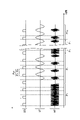
- 第1の周波数を有する第1の高周波電力と前記第1の周波数よりも高い第2の周波数を有する第2の高周波電力とを用いてプラズマ処理チャンバにおいて基板支持台上に配置された基板を処理するプラズマ処理方法であり、前記基板支持台は下部電極を含み、該プラズマ処理方法は、
(a)第1の期間において第1のプラズマ処理を実行する工程であり、前記第1のプラズマ処理は、前記第1の高周波電力を供給することなく前記第2の高周波電力をパルス状に供給することを含む、該工程と、
(b)前記第1の期間とは異なる第2の期間において第2のプラズマ処理を実行する工程であり、前記第2の期間は複数の周期を含み、該複数の周期の各々は第1の電圧出力期間及び該第1の電圧出力期間とは異なる第2の電圧出力期間を含み、前記第2のプラズマ処理は、前記複数の周期の各々において前記第1の高周波電力を前記下部電極に供給すること、前記第1の電圧出力期間において前記第2の高周波電力を供給すること、及び、前記第2の電圧出力期間において前記第2の高周波電力を停止すること、を含む、該工程と、
(c)前記(a)と前記(b)とを繰り返す工程と、
を含み、
前記第2の高周波電力は、前記第2の期間においてパルス状に供給され、前記第2の高周波電力は、前記第1の期間内と前記第2の期間内で同じ周期でパルス状に供給される、
プラズマ処理方法。 - 前記第1の高周波電力は、前記第1の電圧出力期間において負の電位を有する、請求項1に記載のプラズマ処理方法。
- 前記第1の高周波電力は、前記第1の電圧出力期間において正の電位を有する、請求項1に記載のプラズマ処理方法。
- (d)前記(a)及び(b)の後に、前記第1の高周波電力及び前記第2の高周波電力を停止し、前記チャンバを排気する工程を更に含み、
前記(c)は、前記(a)、前記(b)、及び前記(d)を繰り返すことを含む、
請求項1に記載のプラズマ処理方法。 - 前記第1のプラズマ処理と前記第2のプラズマ処理は同一の処理ガスを用いて行われる、請求項1に記載のプラズマ処理方法。
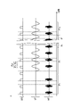
- 第1の周波数を有する第1の高周波電力と前記第1の周波数よりも高い第2の周波数を有する第2の高周波電力とを用いてプラズマ処理チャンバにおいて基板支持台上に配置された基板を処理するプラズマ処理方法であり、前記基板支持台は下部電極を含み、該プラズマ処理方法は、
(a)第1の期間において第1のプラズマ処理を実行する工程であり、前記第1のプラズマ処理は、前記第1の高周波電力を供給することなく前記第2の高周波電力を連続的に又はパルス状に供給することを含む、該工程と、
(b)前記第1の期間とは異なる第2の期間において第2のプラズマ処理を実行する工程であり、前記第2の期間は複数の周期を含み、該複数の周期の各々は第1の電圧出力期間及び該第1の電圧出力期間とは異なる第2の電圧出力期間を含み、前記第2のプラズマ処理は、前記複数の周期の各々において前記第1の高周波電力を前記下部電極に供給すること、前記第1の電圧出力期間において前記第2の高周波電力を供給すること、及び、前記第2の電圧出力期間において前記第2の高周波電力を停止すること、を含む、該工程と、
(c)前記(a)と前記(b)とを繰り返す工程と、
を含み、
前記第1のプラズマ処理と前記第2のプラズマ処理は同一の処理ガスを用いて行われる、プラズマ処理方法。 - プラズマ処理チャンバと、
下部電極を含み、前記チャンバ内に設けられた基板支持台と、
第1の周波数を有する第1の高周波電力を前記下部電極に供給するように構成された第1の高周波電源部と、
前記プラズマ処理チャンバにおいてプラズマを生成するために前記第1の周波数よりも高い第2の周波数を有する第2の高周波電力を供給するように構成された第2の高周波電源部と、
制御部と、
を備え、
前記制御部は、
(a)第1の期間において第1のプラズマ処理を実行し、
(b)前記第1の期間とは異なる第2の期間において第2のプラズマ処理を実行し、
(c)前記(a)と前記(b)とを繰り返す
ように、前記第1の高周波電源部及び前記第2の高周波電源部を制御するように構成され、
前記第1のプラズマ処理は、前記第1の高周波電力を供給することなく前記第2の高周波電力をパルス状に供給することを含み、
前記第2の期間は、複数の周期を含み、該複数の周期の各々は、第1の電圧出力期間及び前記第1の電圧出力期間とは異なる第2の電圧出力期間を含み、
前記第2のプラズマ処理は、前記複数の周期の各々において前記第1の高周波電力を前記下部電極に供給すること、前記第1の電圧出力期間において前記第2の高周波電力を供給すること、及び、前記第2の電圧出力期間において前記第2の高周波電力を停止すること、を含み、
前記第2の高周波電力は、前記第2の期間においてパルス状に供給され、前記第2の高周波電力は、前記第1の期間内と前記第2の期間内で同じ周期でパルス状に供給される、
プラズマ処理装置。 - プラズマ処理チャンバと、
下部電極を含み、前記チャンバ内に設けられた基板支持台と、
第1の周波数を有する第1の高周波電力を前記下部電極に供給するように構成された第1の高周波電源部と、
前記プラズマ処理チャンバにおいてプラズマを生成するために前記第1の周波数よりも高い第2の周波数を有する第2の高周波電力を供給するように構成された第2の高周波電源部と、
制御部と、
を備え、
前記制御部は、
(a)第1の期間において第1のプラズマ処理を実行し、
(b)前記第1の期間とは異なる第2の期間において第2のプラズマ処理を実行し、
(c)前記(a)と前記(b)とを繰り返す
ように、前記第1の高周波電源部及び前記第2の高周波電源部を制御するように構成され、
前記第1のプラズマ処理は、前記第1の高周波電力を供給することなく前記第2の高周波電力を連続的又はパルス状に供給することを含み、
前記第2の期間は、複数の周期を含み、該複数の周期の各々は、第1の電圧出力期間及び前記第1の電圧出力期間とは異なる第2の電圧出力期間を含み、
前記第2のプラズマ処理は、前記複数の周期の各々において前記第1の高周波電力を前記下部電極に供給すること、前記第1の電圧出力期間において前記第2の高周波電力を供給すること、及び、前記第2の電圧出力期間において前記第2の高周波電力を停止すること、を含み、
前記第1のプラズマ処理と前記第2のプラズマ処理は同一の処理ガスを用いて行われる、
プラズマ処理装置。
Priority Applications (5)
| Application Number | Priority Date | Filing Date | Title |
|---|---|---|---|
| JP2018193752A JP7101096B2 (ja) | 2018-10-12 | 2018-10-12 | プラズマ処理方法及びプラズマ処理装置 |
| TW108135619A TWI828773B (zh) | 2018-10-12 | 2019-10-02 | 電漿處理方法及電漿處理裝置 |
| KR1020190123868A KR20200041789A (ko) | 2018-10-12 | 2019-10-07 | 플라즈마 처리 방법 및 플라즈마 처리 장치 |
| CN201910958296.0A CN111048389A (zh) | 2018-10-12 | 2019-10-10 | 等离子体处理方法和等离子体处理装置 |
| US16/599,952 US11282701B2 (en) | 2018-10-12 | 2019-10-11 | Plasma processing method and plasma processing apparatus |
Applications Claiming Priority (1)
| Application Number | Priority Date | Filing Date | Title |
|---|---|---|---|
| JP2018193752A JP7101096B2 (ja) | 2018-10-12 | 2018-10-12 | プラズマ処理方法及びプラズマ処理装置 |
Publications (3)
| Publication Number | Publication Date |
|---|---|
| JP2020061534A JP2020061534A (ja) | 2020-04-16 |
| JP2020061534A5 JP2020061534A5 (ja) | 2021-07-26 |
| JP7101096B2 true JP7101096B2 (ja) | 2022-07-14 |
Family
ID=70160685
Family Applications (1)
| Application Number | Title | Priority Date | Filing Date |
|---|---|---|---|
| JP2018193752A Active JP7101096B2 (ja) | 2018-10-12 | 2018-10-12 | プラズマ処理方法及びプラズマ処理装置 |
Country Status (5)
| Country | Link |
|---|---|
| US (1) | US11282701B2 (ja) |
| JP (1) | JP7101096B2 (ja) |
| KR (1) | KR20200041789A (ja) |
| CN (1) | CN111048389A (ja) |
| TW (1) | TWI828773B (ja) |
Families Citing this family (3)
| Publication number | Priority date | Publication date | Assignee | Title |
|---|---|---|---|---|
| JP6846387B2 (ja) * | 2018-06-22 | 2021-03-24 | 東京エレクトロン株式会社 | プラズマ処理方法及びプラズマ処理装置 |
| CN117480870A (zh) * | 2021-06-21 | 2024-01-30 | 东京毅力科创株式会社 | 等离子体处理装置和等离子体处理方法 |
| WO2023238740A1 (ja) * | 2022-06-08 | 2023-12-14 | 東京エレクトロン株式会社 | エッチング方法及びプラズマ処理装置 |
Citations (2)
| Publication number | Priority date | Publication date | Assignee | Title |
|---|---|---|---|---|
| JP2000269198A (ja) | 1999-03-19 | 2000-09-29 | Toshiba Corp | プラズマ処理方法及びプラズマ処理装置 |
| JP2017216284A (ja) | 2016-05-30 | 2017-12-07 | 東京エレクトロン株式会社 | エッチング方法 |
Family Cites Families (6)
| Publication number | Priority date | Publication date | Assignee | Title |
|---|---|---|---|---|
| JP3210469B2 (ja) | 1993-03-12 | 2001-09-17 | 株式会社日立製作所 | 半導体集積回路装置の製造方法 |
| KR102247560B1 (ko) * | 2014-07-14 | 2021-05-03 | 삼성전자 주식회사 | Rps에서의 플라즈마 생성방법, 및 그 플라즈마 생성방법을 포함한 반도체 소자 제조방법 |
| JP6315809B2 (ja) * | 2014-08-28 | 2018-04-25 | 東京エレクトロン株式会社 | エッチング方法 |
| JP6424120B2 (ja) * | 2015-03-23 | 2018-11-14 | 東京エレクトロン株式会社 | 電源システム、プラズマ処理装置及び電源制御方法 |
| KR102124407B1 (ko) * | 2016-01-18 | 2020-06-18 | 주식회사 히타치하이테크 | 플라스마 처리 방법 및 플라스마 처리 장치 |
| JP6667343B2 (ja) * | 2016-03-30 | 2020-03-18 | 東京エレクトロン株式会社 | プラズマ処理装置およびプラズマ処理方法 |
-
2018
- 2018-10-12 JP JP2018193752A patent/JP7101096B2/ja active Active
-
2019
- 2019-10-02 TW TW108135619A patent/TWI828773B/zh active
- 2019-10-07 KR KR1020190123868A patent/KR20200041789A/ko active Search and Examination
- 2019-10-10 CN CN201910958296.0A patent/CN111048389A/zh active Pending
- 2019-10-11 US US16/599,952 patent/US11282701B2/en active Active
Patent Citations (2)
| Publication number | Priority date | Publication date | Assignee | Title |
|---|---|---|---|---|
| JP2000269198A (ja) | 1999-03-19 | 2000-09-29 | Toshiba Corp | プラズマ処理方法及びプラズマ処理装置 |
| JP2017216284A (ja) | 2016-05-30 | 2017-12-07 | 東京エレクトロン株式会社 | エッチング方法 |
Also Published As
| Publication number | Publication date |
|---|---|
| TW202025286A (zh) | 2020-07-01 |
| US20200118814A1 (en) | 2020-04-16 |
| KR20200041789A (ko) | 2020-04-22 |
| TWI828773B (zh) | 2024-01-11 |
| US11282701B2 (en) | 2022-03-22 |
| CN111048389A (zh) | 2020-04-21 |
| JP2020061534A (ja) | 2020-04-16 |
Similar Documents
| Publication | Publication Date | Title |
|---|---|---|
| US11871503B2 (en) | Plasma processing method and plasma processing apparatus | |
| KR102361782B1 (ko) | 에칭 방법 | |
| JP7101096B2 (ja) | プラズマ処理方法及びプラズマ処理装置 | |
| JP7374362B2 (ja) | プラズマ処理方法及びプラズマ処理装置 | |
| TWI719958B (zh) | 電漿蝕刻方法 | |
| JP7250663B2 (ja) | プラズマ処理装置及びインピーダンスの整合方法 | |
| US11017985B2 (en) | Plasma processing apparatus, impedance matching method, and plasma processing method | |
| US20200144028A1 (en) | Plasma processing apparatus and plasma processing method | |
| KR20200144479A (ko) | 플라즈마 처리 방법 및 플라즈마 처리 장치 | |
| JP6928548B2 (ja) | エッチング方法 | |
| JP2020177959A (ja) | クリーニング処理方法及びプラズマ処理装置 | |
| KR20210035073A (ko) | 플라즈마 처리 방법 및 플라즈마 처리 장치 | |
| JP7229033B2 (ja) | 基板処理方法及び基板処理装置 | |
| JP2021114551A (ja) | エッチング方法及びプラズマ処理装置 | |
| JP2022032235A (ja) | エッチング方法及びプラズマ処理装置 |
Legal Events
| Date | Code | Title | Description |
|---|---|---|---|
| A521 | Request for written amendment filed |
Free format text: JAPANESE INTERMEDIATE CODE: A523 Effective date: 20210525 |
|
| A621 | Written request for application examination |
Free format text: JAPANESE INTERMEDIATE CODE: A621 Effective date: 20210525 |
|
| A977 | Report on retrieval |
Free format text: JAPANESE INTERMEDIATE CODE: A971007 Effective date: 20220330 |
|
| A131 | Notification of reasons for refusal |
Free format text: JAPANESE INTERMEDIATE CODE: A131 Effective date: 20220405 |
|
| A521 | Request for written amendment filed |
Free format text: JAPANESE INTERMEDIATE CODE: A523 Effective date: 20220517 |
|
| TRDD | Decision of grant or rejection written | ||
| A01 | Written decision to grant a patent or to grant a registration (utility model) |
Free format text: JAPANESE INTERMEDIATE CODE: A01 Effective date: 20220607 |
|
| A61 | First payment of annual fees (during grant procedure) |
Free format text: JAPANESE INTERMEDIATE CODE: A61 Effective date: 20220704 |
|
| R150 | Certificate of patent or registration of utility model |
Ref document number: 7101096 Country of ref document: JP Free format text: JAPANESE INTERMEDIATE CODE: R150 |