WO2019244382A1 - 配線基板および半導体装置 - Google Patents
配線基板および半導体装置 Download PDFInfo
- Publication number
- WO2019244382A1 WO2019244382A1 PCT/JP2019/001122 JP2019001122W WO2019244382A1 WO 2019244382 A1 WO2019244382 A1 WO 2019244382A1 JP 2019001122 W JP2019001122 W JP 2019001122W WO 2019244382 A1 WO2019244382 A1 WO 2019244382A1
- Authority
- WO
- WIPO (PCT)
- Prior art keywords
- conductive layer
- insulating layer
- wiring board
- layer
- substrate
- Prior art date
- Legal status (The legal status is an assumption and is not a legal conclusion. Google has not performed a legal analysis and makes no representation as to the accuracy of the status listed.)
- Ceased
Links
Images















Classifications
-
- H—ELECTRICITY
- H05—ELECTRIC TECHNIQUES NOT OTHERWISE PROVIDED FOR
- H05K—PRINTED CIRCUITS; CASINGS OR CONSTRUCTIONAL DETAILS OF ELECTRIC APPARATUS; MANUFACTURE OF ASSEMBLAGES OF ELECTRICAL COMPONENTS
- H05K1/00—Printed circuits
- H05K1/16—Printed circuits incorporating printed electric components, e.g. printed resistors, capacitors or inductors
-
- H—ELECTRICITY
- H05—ELECTRIC TECHNIQUES NOT OTHERWISE PROVIDED FOR
- H05K—PRINTED CIRCUITS; CASINGS OR CONSTRUCTIONAL DETAILS OF ELECTRIC APPARATUS; MANUFACTURE OF ASSEMBLAGES OF ELECTRICAL COMPONENTS
- H05K3/00—Apparatus or processes for manufacturing printed circuits
- H05K3/46—Manufacturing multilayer circuits
-
- H—ELECTRICITY
- H10—SEMICONDUCTOR DEVICES; ELECTRIC SOLID-STATE DEVICES NOT OTHERWISE PROVIDED FOR
- H10D—INORGANIC ELECTRIC SEMICONDUCTOR DEVICES
- H10D1/00—Resistors, capacitors or inductors
- H10D1/60—Capacitors
- H10D1/68—Capacitors having no potential barriers
-
- H—ELECTRICITY
- H10—SEMICONDUCTOR DEVICES; ELECTRIC SOLID-STATE DEVICES NOT OTHERWISE PROVIDED FOR
- H10W—GENERIC PACKAGES, INTERCONNECTIONS, CONNECTORS OR OTHER CONSTRUCTIONAL DETAILS OF DEVICES COVERED BY CLASS H10
- H10W20/00—Interconnections in chips, wafers or substrates
- H10W20/40—Interconnections external to wafers or substrates, e.g. back-end-of-line [BEOL] metallisations or vias connecting to gate electrodes
- H10W20/41—Interconnections external to wafers or substrates, e.g. back-end-of-line [BEOL] metallisations or vias connecting to gate electrodes characterised by their conductive parts
- H10W20/42—Vias, e.g. via plugs
-
- H—ELECTRICITY
- H10—SEMICONDUCTOR DEVICES; ELECTRIC SOLID-STATE DEVICES NOT OTHERWISE PROVIDED FOR
- H10W—GENERIC PACKAGES, INTERCONNECTIONS, CONNECTORS OR OTHER CONSTRUCTIONAL DETAILS OF DEVICES COVERED BY CLASS H10
- H10W70/00—Package substrates; Interposers; Redistribution layers [RDL]
- H10W70/01—Manufacture or treatment
- H10W70/05—Manufacture or treatment of insulating or insulated package substrates, or of interposers, or of redistribution layers
- H10W70/095—Manufacture or treatment of insulating or insulated package substrates, or of interposers, or of redistribution layers of vias therein
-
- H—ELECTRICITY
- H10—SEMICONDUCTOR DEVICES; ELECTRIC SOLID-STATE DEVICES NOT OTHERWISE PROVIDED FOR
- H10W—GENERIC PACKAGES, INTERCONNECTIONS, CONNECTORS OR OTHER CONSTRUCTIONAL DETAILS OF DEVICES COVERED BY CLASS H10
- H10W70/00—Package substrates; Interposers; Redistribution layers [RDL]
- H10W70/60—Insulating or insulated package substrates; Interposers; Redistribution layers
- H10W70/62—Insulating or insulated package substrates; Interposers; Redistribution layers characterised by their interconnections
- H10W70/63—Vias, e.g. via plugs
- H10W70/635—Through-vias
-
- H—ELECTRICITY
- H10—SEMICONDUCTOR DEVICES; ELECTRIC SOLID-STATE DEVICES NOT OTHERWISE PROVIDED FOR
- H10W—GENERIC PACKAGES, INTERCONNECTIONS, CONNECTORS OR OTHER CONSTRUCTIONAL DETAILS OF DEVICES COVERED BY CLASS H10
- H10W70/00—Package substrates; Interposers; Redistribution layers [RDL]
- H10W70/60—Insulating or insulated package substrates; Interposers; Redistribution layers
- H10W70/67—Insulating or insulated package substrates; Interposers; Redistribution layers characterised by their insulating layers or insulating parts
- H10W70/68—Shapes or dispositions thereof
- H10W70/685—Shapes or dispositions thereof comprising multiple insulating layers
-
- H—ELECTRICITY
- H10—SEMICONDUCTOR DEVICES; ELECTRIC SOLID-STATE DEVICES NOT OTHERWISE PROVIDED FOR
- H10D—INORGANIC ELECTRIC SEMICONDUCTOR DEVICES
- H10D1/00—Resistors, capacitors or inductors
- H10D1/60—Capacitors
- H10D1/68—Capacitors having no potential barriers
- H10D1/682—Capacitors having no potential barriers having dielectrics comprising perovskite structures
-
- H—ELECTRICITY
- H10—SEMICONDUCTOR DEVICES; ELECTRIC SOLID-STATE DEVICES NOT OTHERWISE PROVIDED FOR
- H10P—GENERIC PROCESSES OR APPARATUS FOR THE MANUFACTURE OR TREATMENT OF DEVICES COVERED BY CLASS H10
- H10P95/00—Generic processes or apparatus for manufacture or treatments not covered by the other groups of this subclass
- H10P95/06—Planarisation of inorganic insulating materials
- H10P95/062—Planarisation of inorganic insulating materials involving a dielectric removal step
-
- H—ELECTRICITY
- H10—SEMICONDUCTOR DEVICES; ELECTRIC SOLID-STATE DEVICES NOT OTHERWISE PROVIDED FOR
- H10W—GENERIC PACKAGES, INTERCONNECTIONS, CONNECTORS OR OTHER CONSTRUCTIONAL DETAILS OF DEVICES COVERED BY CLASS H10
- H10W20/00—Interconnections in chips, wafers or substrates
- H10W20/20—Interconnections within wafers or substrates, e.g. through-silicon vias [TSV]
-
- H—ELECTRICITY
- H10—SEMICONDUCTOR DEVICES; ELECTRIC SOLID-STATE DEVICES NOT OTHERWISE PROVIDED FOR
- H10W—GENERIC PACKAGES, INTERCONNECTIONS, CONNECTORS OR OTHER CONSTRUCTIONAL DETAILS OF DEVICES COVERED BY CLASS H10
- H10W20/00—Interconnections in chips, wafers or substrates
- H10W20/40—Interconnections external to wafers or substrates, e.g. back-end-of-line [BEOL] metallisations or vias connecting to gate electrodes
- H10W20/495—Capacitive arrangements or effects of, or between wiring layers
- H10W20/496—Capacitor integral with wiring layers
-
- H—ELECTRICITY
- H10—SEMICONDUCTOR DEVICES; ELECTRIC SOLID-STATE DEVICES NOT OTHERWISE PROVIDED FOR
- H10W—GENERIC PACKAGES, INTERCONNECTIONS, CONNECTORS OR OTHER CONSTRUCTIONAL DETAILS OF DEVICES COVERED BY CLASS H10
- H10W20/00—Interconnections in chips, wafers or substrates
- H10W20/40—Interconnections external to wafers or substrates, e.g. back-end-of-line [BEOL] metallisations or vias connecting to gate electrodes
- H10W20/497—Inductive arrangements or effects of, or between, wiring layers
Definitions
- the present disclosure relates to a wiring board.
- MIMIM (Metal-Insulator-Metal) capacitors may be formed on a substrate with wiring.
- This capacitor has a structure in which an insulating layer is sandwiched between conductive layers.
- the conductive layer and the insulating layer have different coefficients of thermal expansion. Therefore, stress is generated by expansion and contraction according to the heat history due to the manufacturing process and the like. This phenomenon becomes more remarkable when the wiring is made thicker to reduce the transmission resistance.
- the insulating layer is separated from the conductive layer or cracks are generated in the insulating layer in order to reduce the stress. As described above, the generation of a large stress causes a reduction in the reliability of the capacitor.
- Patent Literature 1 discloses a technique in which an insulating layer is an elastic body for stress relaxation. This elastic body is an organic material.
- Organic materials generally have a large dielectric loss tangent. Therefore, when a high-frequency signal is applied to the conductive layer, a large transmission loss occurs and power efficiency deteriorates. When the power loss is converted into heat, the heat deteriorates the performance of the device, such as deterioration of device characteristics and deterioration of signal quality due to thermal noise. As described above, in the structure disclosed in Patent Literature 1, even if the stress can be relaxed, the performance of the element is reduced.
- One of the objects of the present disclosure is to improve the reliability of a capacitor.
- a substrate having an insulating surface, a first conductive layer disposed on the substrate, a first portion having a first thickness, and a second thickness smaller than the first thickness.
- a first conductive layer including a second portion adjacent to the first portion, a first insulating layer disposed on the first portion at a distance from the second portion, and a first insulating layer. And a second conductive layer disposed on a side opposite to the first portion.
- the first portion and the second portion may include a region formed of the same material on the first insulating layer side.
- the first conductive layer includes a first film and a second film having a different film quality from the first film, and the second film is disposed between the first film and the first insulating layer;
- the second film in the second portion may be thinner than the second film in the first portion.
- the second conductive layer may be disposed apart from a first edge of the edge of the first insulating layer corresponding to the second portion.
- an edge of the second conductive layer and a first edge corresponding to the second portion side of the edge of the first insulating layer are It may include aligned parts.
- the distance from the boundary between the first portion and the second portion to the first edge is from the edge of the second conductive layer. It may be smaller than the distance to the first edge.
- the distance from the boundary between the first portion and the second portion to the edge of the first insulating layer is the first thickness and the second thickness. It may be smaller than the difference from the thickness.
- the boundary may be disposed between the first insulating layer and the substrate.
- the distance from the boundary between the first portion and the second portion to the edge of the second portion when viewed along the normal direction of the surface of the substrate is the first thickness and the second thickness. May be larger than the difference between the two.
- the distance from the boundary between the first portion and the second portion to the edge of the second portion when viewed along the normal direction of the surface of the substrate is 10% or more of the second thickness. There may be.
- the first portion may be surrounded by the second portion.
- the outer edge of the first conductive layer may include a side surface of the first portion and a side surface of the second portion when viewed along a normal direction of the surface of the substrate.
- the first insulating layer may cover a side surface of the first portion.
- Part of the first insulating layer may be sandwiched between the second conductive layer and a side surface of the first portion.
- the surface of the second part may be rougher than the surface of the first part.
- the first conductive layer may include at least a first film and a second film having a different film quality from the first film.
- a recess formed on the side surface of the first film and the side surface of the second film may be arranged on the side surface of the first conductive layer.
- It may further include a second insulating layer in contact with the second portion and the first insulating layer, wherein the first insulating layer includes an inorganic material, and the second insulating layer may include an organic material.
- the second insulating layer has an opening, the second conductive layer is in contact with a side surface of the second insulating layer that defines the opening, and is provided between the second conductive layer and the first insulating layer.
- the second insulating layer may be partially disposed.
- the semiconductor device may further include a conductive layer disposed on a side opposite to the first portion with respect to the first insulating layer and separated from the second conductive layer.
- the first conductive layer further includes a third portion having a third thickness greater than the second thickness and adjacent to the second portion, and the first insulating layer is further disposed on the third portion.
- the second conductive layer may be disposed on a side opposite to the third portion with respect to the first insulating layer.
- the semiconductor device may further include a through electrode penetrating the substrate, and the through electrode may be electrically connected to the first conductive layer.
- the through electrode may be formed of the same material as the first conductive layer, and may extend continuously from the first conductive layer.
- the first conductive layer includes a plurality of films
- the through electrode includes a plurality of films
- a film closest to the substrate in the first conductive layer is continuously formed until a film in the first through electrode closest to the substrate. It may extend.
- It may further include an inductor including the through electrode connected to the first conductive layer.
- a semiconductor device including the above-described wiring board and a semiconductor chip electrically connected to the wiring board.
- the reliability of the capacitor can be improved.
- FIG. 1 is a schematic plan view illustrating an interposer according to a first embodiment of the present disclosure.
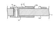
- FIG. 2 is a schematic cross-sectional view (a cross-sectional view along the line AA in FIG. 1) illustrating the interposer according to the first embodiment of the present disclosure.
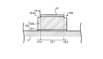
- FIG. 2 is a schematic cross-sectional view (a cross-sectional view taken along line BB of FIG. 1) illustrating a capacitor included in the interposer according to the first embodiment of the present disclosure.
- FIG. 2 is an enlarged view of the vicinity of a step portion of the capacitor according to the first embodiment of the present disclosure.
- FIG. 4 is a diagram illustrating a method of manufacturing the interposer according to the first embodiment of the present disclosure.
- FIG. 4 is a diagram illustrating a method of manufacturing the interposer according to the first embodiment of the present disclosure.
- FIG. 4 is a diagram illustrating a method of manufacturing the interposer according to the first embodiment of the present disclosure.
- FIG. 4 is a diagram illustrating a method of manufacturing the interposer according to the first embodiment of the present disclosure.
- FIG. 4 is a diagram illustrating a method of manufacturing the interposer according to the first embodiment of the present disclosure.
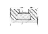
- FIG. 3 is a diagram illustrating a method for manufacturing the capacitor according to the first embodiment of the present disclosure.
- FIG. 3 is a diagram illustrating a method for manufacturing the capacitor according to the first embodiment of the present disclosure.
- FIG. 3 is a diagram illustrating a method for manufacturing the capacitor according to the first embodiment of the present disclosure.
- FIG. 3 is a diagram illustrating a method for manufacturing the capacitor according to the first embodiment of the present disclosure.
- FIG. 3 is a diagram illustrating a method for manufacturing the capacitor according to the first embodiment of the present disclosure.
- FIG. 3 is a diagram illustrating a method for manufacturing the capacitor according to the first embodiment of the present disclosure.
- FIG. 3 is a diagram illustrating a method for manufacturing the capacitor according to the first embodiment of the present disclosure.
- FIG. 9 is a diagram illustrating a stress distribution of a first conductive layer of a capacitor in a comparative example.
- FIG. 2 is a diagram illustrating a stress distribution of a first conductive layer of the capacitor according to the first embodiment of the present disclosure.
- FIG. 5 is a diagram illustrating another method for manufacturing the capacitor according to the first embodiment of the present disclosure.
- FIG. 5 is a diagram illustrating another method for manufacturing the capacitor according to the first embodiment of the present disclosure.
- FIG. 5 is a diagram illustrating another method for manufacturing the capacitor according to the first embodiment of the present disclosure.
- FIG. 11 is a diagram illustrating a method for manufacturing a capacitor according to the second embodiment of the present disclosure.
- FIG. 11 is a diagram illustrating a method for manufacturing a capacitor according to the second embodiment of the present disclosure.
- FIG. 11 is a diagram illustrating a method for manufacturing a capacitor according to the second embodiment of the present disclosure.
- FIG. 11 is a diagram illustrating a method for manufacturing a capacitor according to the second embodiment of the present disclosure.
- It is a schematic plan view showing an interposer according to a third embodiment of the present disclosure.
- FIG. 25 is a schematic cross-sectional view (a cross-sectional view taken along the line BB of FIG. 24) illustrating a capacitor included in the interposer according to the third embodiment of the present disclosure.
- FIG. 27 is a schematic cross-sectional view (a cross-sectional view taken along line BB of FIG. 26) illustrating a capacitor included in an interposer according to a fourth embodiment of the present disclosure. It is a schematic plan view showing an interposer according to a fifth embodiment of the present disclosure. It is a schematic plan view showing an interposer according to a sixth embodiment of the present disclosure. It is a schematic plan view showing an interposer according to a seventh embodiment of the present disclosure.
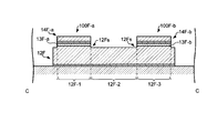
- FIG. 31 is a schematic cross-sectional view (a cross-sectional view taken along line CC in FIG. 30) illustrating a capacitor according to a seventh embodiment of the present disclosure.
- FIG. 2 is a schematic cross-sectional view illustrating a side surface shape of a first conductive layer according to the first embodiment of the present disclosure.
- FIG. 21 is a schematic cross-sectional view illustrating a side surface shape of a first conductive layer according to a tenth embodiment of the present disclosure.
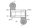
- FIG. 21 is a schematic plan view illustrating an interposer according to an eleventh embodiment of the present disclosure.
- FIG. 37 is a schematic sectional view (a sectional view taken along line DD of FIG.
- FIG. 21 is a schematic cross-sectional view illustrating a capacitor according to a twelfth embodiment of the present disclosure.
- FIG. 21 is a schematic plan view illustrating capacitors and inductors included in an interposer according to a thirteenth embodiment of the present disclosure.
- FIG. 39 is a schematic cross-sectional view (a cross-sectional view taken along the line EE of FIG. 39) illustrating an interposer according to a thirteenth embodiment of the present disclosure.
- FIG. 21 is a schematic sectional view illustrating a capacitor according to a fourteenth embodiment of the present disclosure.
- FIG. 21 is a diagram illustrating a method for manufacturing a capacitor according to a fourteenth embodiment of the present disclosure.
- FIG. 21 is a diagram illustrating a method for manufacturing a capacitor according to a fourteenth embodiment of the present disclosure.
- FIG. 21 is a diagram illustrating a semiconductor device according to a fifteenth embodiment of the present disclosure.
- FIG. 21 is a diagram illustrating another example of a semiconductor device according to a fifteenth embodiment of the present disclosure.
- FIG. 39 is a diagram illustrating yet another example of a semiconductor device according to a fifteenth embodiment of the present disclosure.
- FIG. 21 is a diagram illustrating an example of an electronic apparatus including a semiconductor device according to a fifteenth embodiment of the present disclosure.
- An interposer has a MIM structure in which an insulating layer is sandwiched between conductive layers containing metal or the like.
- the MIM structure will be described as a capacitor in which an insulating layer, which is a dielectric layer, is sandwiched between an upper electrode and a lower electrode.
- the stress particularly strong generated at the end of the insulating layer on the lower electrode can be reduced as compared with the conventional capacitor.
- the structure of the interposer having such a capacitor will be specifically described.
- FIG. 1 is a schematic plan view showing an interposer 10 according to the first embodiment of the present disclosure.
- FIG. 2 is a schematic cross-sectional view (cross-sectional view along the line AA in FIG. 1) illustrating the interposer 10 according to the first embodiment of the present disclosure.
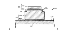
- FIG. 3 is a schematic cross-sectional view (a cross-sectional view taken along line BB of FIG. 1) showing the capacitor 100 included in the interposer 10 according to the first embodiment of the present disclosure. 1 and 3, some components are omitted so that the positional relationship among the substrate 11, the first conductive layer 12, the first insulating layer 13, and the second conductive layer 14 can be easily understood.
- the first conductive layer 12 corresponds to a lower electrode
- the first insulating layer 13 corresponds to a dielectric layer
- the second conductive layer 14 corresponds to an upper electrode.
- the interposer 10 includes a substrate 11, a first conductive layer 12, a first insulating layer 13, and a second conductive layer 14.
- the substrate 11 has a first surface 11a and a second surface 11b opposite to the first surface 11a.
- the substrate 11 is a substrate having an insulating surface, and in this example, is non-alkali glass.
- the substrate 11 may be an inorganic insulating material other than glass, may be an organic material, may be a semiconductor substrate, or may be an organic material. Desirably, it has an insulating property at least on the surface.
- the thickness of the substrate 11 is preferably 50 ⁇ m or more and 700 ⁇ m or less, and in this example, it is 400 ⁇ m.
- the surface roughness (arithmetic mean roughness Ra) of the first surface 11a of the substrate 11 is determined by the first conductive layer 12 formed on the first surface 11a of the substrate 11 and the fourth conductive layer 12 formed on the second surface 11b. From the viewpoint of preventing transmission loss from occurring in a high-frequency signal in the layer 21, the thickness is preferably 50 nm or less, particularly preferably 0.1 nm to 30 nm.
- the arithmetic average roughness Ra follows the definition according to JIS standard JIS B 0601: 2001.
- the term surface roughness corresponds to the arithmetic average roughness Ra.
- the first conductive layer 12 includes a first lower conductive layer 121 and a first upper conductive layer 123.
- the first lower conductive layer 121 is disposed on the first surface 11a of the substrate 11.
- the first upper conductive layer 123 is disposed on the first lower conductive layer 121.
- a step 12s is formed along the edge of the first insulating layer 13. The presence of the step 12s alleviates the stress on the first insulating layer 13. The detailed structure of the step 12s will be described later.
- the first lower conductive layer 121 may be directly disposed on the first surface 11a of the substrate 11, or a conductive or insulating layer may be disposed on the first surface 11a of the substrate 11 via at least one layer. It may be.
- an insulating resin on the first surface 11a of the substrate 11, the stress generated due to the difference in the coefficient of thermal expansion between the first conductive layer 12 and the substrate 11 can be reduced.
- the insulating resin include epoxy, polyimide, polybenzoxazole, and polyamide.
- the first lower conductive layer 121 corresponds to a part of the seed layer.
- the seed layer is a conductive layer that functions as an electrode when the first upper conductive layer 123 is formed by electrolytic plating.
- the first lower conductive layer 121 is a copper (Cu) film in this example, but may be another film such as chromium (Cr), titanium (Ti), or a plurality of films. Is also good.
- the thickness of the first lower conductive layer 121 is preferably not less than 20 nm and not more than 800 nm, and is 200 nm in this example.
- the first lower conductive layer 121 is formed by an electroless plating method.
- Another layer may be arranged between the first lower conductive layer 121 and the first surface 11a.
- an adhesion layer for preventing the first lower conductive layer 121 from being easily separated from the substrate 11 may be provided.
- the adhesion layer for example, zinc oxide (ZnO) is exemplified.
- the adhesion layer containing zinc oxide is formed by, for example, a sol-gel method.
- the first upper conductive layer 123 is formed by an electrolytic plating method using the first lower conductive layer 121 as a seed layer.
- the first upper conductive layer 123 is a Cu film in this example, but may be a film of another conductive material or may be formed of a plurality of films.
- the thickness of the first upper conductive layer 123 is preferably 0.5 ⁇ m or more and 30 ⁇ m or less, and is 20 ⁇ m in this example.
- the first insulating layer 13 is disposed on the first conductive layer 12.
- the first insulating layer 13 is a film of silicon nitride (SiN), but silicon oxide (SiO), silicon oxynitride (SiON), tantalum oxide (TaO), aluminum oxide (AlO), aluminum nitride (AlN). It may be a film of an inorganic material such as AlN), hafnium oxide (HfO), or a plurality of films. It is desirable that the relative permittivity of the first insulating layer 13 be higher than that of the insulating layer (for example, the second insulating layer 22) existing around the capacitor 100.
- the relative dielectric constant of the first insulating layer 13 is, for example, 2.0 or more and 9.0 or less, and more preferably 5.0 or more and 8.0 or less.
- the thickness of the first insulating layer 13 is preferably 50 nm or more and 800 nm or less, and is 500 nm in this example.
- the first insulating layer 13 is formed by chemical vapor deposition (CVD).
- the second conductive layer 14 is disposed on the first insulating layer 13.
- the second conductive layer 14 includes a second lower conductive layer 141 and a second upper conductive layer 143.
- the second lower conductive layer 141 is disposed on the first insulating layer 13.
- the second upper conductive layer 143 is disposed on the second lower conductive layer 141.
- the second lower conductive layer 141 corresponds to a part of the seed layer.
- the seed layer is a conductive layer that functions as an electrode when the second upper conductive layer 143 is formed by electrolytic plating.
- the second lower conductive layer 141 is a copper (Cu) film, but may be another film such as chromium (Cr), titanium (Ti), or a plurality of films. Is also good.
- the thickness of the second lower conductive layer 141 is preferably 20 nm or more and 400 nm or less, and is 200 nm in this example.
- the second lower conductive layer 141 is formed by an electroless plating method.
- the second upper conductive layer 143 is formed by an electrolytic plating method using the second lower conductive layer 141 as a seed layer.
- the second upper conductive layer 143 is a Cu film, but may be a film of another conductive material, or may be formed of a plurality of films.
- the thickness of the second upper conductive layer 143 is preferably 0.5 ⁇ m or more and 5 ⁇ m or less, and is 2 ⁇ m in this example.
- the substrate 11 has a through hole 15 penetrating the first surface 11a and the second surface 11b.
- the first conductive layer 12 is electrically connected to a fourth conductive layer 21 disposed on the second surface 11b via a third conductive layer 20 formed in the through hole 15.
- the third conductive layer 20 is a through electrode that passes through the through hole 15.
- the third conductive layer 20 extends continuously from the first conductive layer 12.
- the third conductive layer 20 includes an outer peripheral portion 201 and an inner peripheral portion 203 in order from the inner surface 15a side of the through hole 15.
- the outer peripheral portion 201 is arranged continuously to the first lower conductive layer 121.
- the inner peripheral portion 203 is disposed continuously to the first upper conductive layer 123.
- the first lower conductive layer 121 extends continuously to the outer peripheral portion 201, and the first upper conductive layer 123 continuously extends to the inner peripheral portion 203.
- another layer such as the above-mentioned adhesion layer may be further disposed between the outer peripheral portion 201 and the inner side surface 15a.
- the opening width of the through hole 15 is preferably 40 ⁇ m or more and 110 ⁇ m or less, and in this example, 80 ⁇ m.
- the opening width of the through-hole 15 defines a figure formed by a cross section of the through-hole 15 along the first surface 11a and the second surface 11b, and an arbitrary outer edge of the figure. Means the maximum distance between the two points.
- the figure formed by the outer edge is a circle, the above-mentioned width refers to the diameter of the circle.
- the through hole 15 has the same opening width between the first surface 11a and the second surface 11b, that is, the through hole 15 has a cylindrical shape, but may have another shape.
- the size of the opening width may change between the first surface 11a and the second surface 11b.
- the opening width may have a minimum value, a maximum value, or a minimum value. Values and local maxima. Further, the opening width may gradually increase from the first surface 11a to the second surface 11b, or may gradually decrease.
- the through hole 15 is formed by performing etching, laser processing, a combination of laser processing and etching, sandblasting, electric discharge machining, drilling, and the like on the substrate 11.
- the third conductive layer 20 is not limited to the form in which the conductive material is arranged along the side surface of the through-hole 15 as shown in FIG. 2, and may have a form in which the through-hole 15 is filled with the conductive material.
- the first conductive layer 12, the third conductive layer 20, and the fourth conductive layer 21 may be at least partially integrated with each other and electrically connected. Further, at least two of the first conductive layer 12, the third conductive layer 20, and the fourth conductive layer 21 may be formed of the same material.
- the fourth conductive layer 21 includes a fourth lower conductive layer 211 and a fourth upper conductive layer 213 in order from the second surface 11b side of the substrate 11.
- the fourth lower conductive layer 211 is arranged continuously to the outer peripheral portion 201.
- the fourth upper conductive layer 213 is disposed continuously to the inner peripheral portion 203.
- another layer such as the above-described adhesion layer may be further disposed between the fourth lower conductive layer 211 and the second surface 11b.
- the first conductive layer 12 and the fourth conductive layer 21 may be formed of the same material and may have substantially the same thickness. In such a case, there is little difference in the resistance value at the connection portion when the connection is made electrically, so that the signal transmission loss can be reduced.
- a second insulating layer 22 which is an example of an insulating layer, is formed.
- the second insulating layer 22 is a layer containing a resin that is an organic material.
- via holes 23 are formed at positions corresponding to the first conductive layer 12, the second conductive layer 14, and the fourth conductive layer 21.
- a connection portion 24 formed of a conductive material is arranged in each of the via holes 23. The connection part 24 is electrically connected to a conductive layer disposed at the bottom of the via hole 23.
- the interposer 10 is electrically connected to the semiconductor chip 50 via the connection unit 24. Further, the interposer 10 is connected to the circuit board 40 via the solder balls 25 and the connection portions 24. The semiconductor chip 50 may also be connected to the connection part 24 via the solder ball 25. According to this configuration, the interposer 10, the semiconductor chip 50 disposed on the first surface 11 a side of the substrate 11 and electrically connected to the third conductive layer 20, and the semiconductor chip 50 disposed on the second surface 11 b side of the substrate 11 And a circuit board 40 electrically connected to the third conductive layer 20. According to the interposer 10 of the present embodiment, the mounting of the semiconductor chips 50 having a narrow terminal pitch on the large circuit board 40 is simplified.
- the circuit board 40 is, for example, a motherboard.
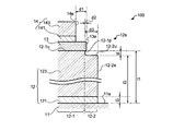
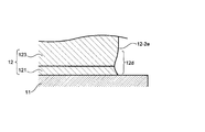
- the first conductive layer 12 includes a first portion 12-1 which is a region in contact with the first insulating layer 13, and a second portion 12-2 which is a region separated from the first insulating layer 13. That is, the upper surface 12-1u of the first portion 12-1 contacts the first insulating layer 13. On the other hand, the upper surface 12-2u of the second portion 12-2 is separated from the first insulating layer 13. The surface roughness of the upper surface 12-2u is equal to or larger than the surface roughness of the upper surface 12-1u.
- the surface roughness of the upper surface 12-1u is 200 nm or less, and the surface roughness of the upper surface 12-2u is 80 nm or more and 300 nm or less. Since the surface roughness of the upper surface 12-1u of the first conductive layer 12 that is in contact with the first insulating layer 13 is small, dielectric breakdown of the first insulating layer 13 in the capacitor 100 is less likely to occur. On the other hand, it is preferable that the surface roughness of the upper surface 12-2u is large because the adhesion to the second insulating layer 22 is improved.
- ⁇ t1 corresponds to the thickness of the first portion 12-1, that is, the distance from the first surface 11a of the substrate 11 to the upper surface 12-1u.
- t2 corresponds to the thickness of the second portion 12-2, that is, the distance from the first surface 11a of the substrate 11 to the upper surface 12-2u.
- the second portion 12-2 is thinner than the first portion 12-1 (t1> t2).
- ts corresponds to the difference (t1-t2) between t1 and t2.
- ts corresponds to the height difference between the upper surface 12-1u and the upper surface 12-2u, that is, the size of the step 12s.
- t3 corresponds to the thickness of the first lower conductive layer 121.
- t1 corresponds to the thickness of the first conductive layer 12, as described above, it corresponds to the thickness obtained by adding the thickness t3 of the first lower conductive layer 121 and the thickness of the first upper conductive layer 123.
- the thickness of the first upper conductive layer 123 in the first part 12-1 corresponds to "t1-t3”
- the thickness of the first upper conductive layer 123 in the second part 12-2 is "t2-t3". ". Therefore, it can be said that the first upper conductive layer 123 in the second portion 12-2 is thinner than the first upper conductive layer 123 in the first portion 12-1.
- t3 is 0.4 ⁇ m
- the thickness of the first upper conductive layer 123 is 20 ⁇ m. Therefore, t1 is 20.4 ⁇ m.
- t2 is 20.1 ⁇ m and ts is 0.3 ⁇ m.
- D1 corresponds to the distance between the side surface 14e of the second conductive layer 14 and the side surface 13e of the first insulating layer 13.
- d2 corresponds to the distance between the boundary 12-1p and the side surface 13e.
- the boundary 12-1p is a boundary between the first portion 12-1 and the second portion 12-2, and is disposed between the first insulating layer 13 and the substrate 11.
- d3 corresponds to the distance between the side surface 12-2e of the second portion 12-2 and the boundary 12-1p.
- the distances d1, d2, and d3 are all distances when viewed perpendicular to the surface (first surface 11a) of the substrate 11, that is, when viewed along the normal direction of the surface of the substrate 11. Corresponds to distance.
- d1 is 10 ⁇ m
- d2 is 0.2 ⁇ m
- d3 is 10 ⁇ m.
- d1 is the distance between the first insulating layer 13 and the second conductive layer 14 required according to the alignment accuracy of the lithography tool when forming the second conductive layer 14, or the first conductive layer 12 and the second conductive layer 14 The length may be larger or smaller than 10 ⁇ m, depending on the distance or the like necessary to prevent short circuit with.
- the side surface 13e and the side surface 14e substantially coincide with each other, and d1 may be 0 ⁇ m in some cases. The case where d1 is 0 ⁇ m will be further described in an embodiment described later.
- d2 is preferably smaller than ts, and may be 0 ⁇ m in some cases.
- d3 may be larger or smaller than 10 ⁇ m. However, d3 does not become 0 ⁇ m.
- d3 is preferably larger than ts, and more preferably larger than d1.
- d3 is preferably 10% or more of t1, and more preferably 30% or more.
- the boundary 12-1p, the side surface 12-2e, the side surface 13e, and the side surface 14e have an edge of the first portion 12-1, an edge of the second portion 12-2 when viewed perpendicular to the surface of the substrate 11, It corresponds to the edge of the first insulating layer 13 and the edge of the second conductive layer 14, respectively.
- the boundary 12-1p can be said to be the outermost position of the first conductive layer 12 that contacts the first insulating layer 13.
- the position of the side surface 12-2e is defined as the outermost position of the second portion 12-2.
- the position of the side surface 14 e is defined as a position in contact with the first insulating layer 13.
- the position of the side surface 13 e is defined as the outermost position of the first insulating layer 13.
- FIGS. 5 to 9 are diagrams illustrating a method of manufacturing the interposer according to the first embodiment of the present disclosure.
- 5 to 9 each show a cross-sectional shape (a cross-sectional view taken along line AA in FIG. 1) of a portion corresponding to FIG.
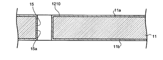
- a substrate 11 having a first surface 11a and a second surface 11b and having a through-hole 15 penetrating the first surface 11a and the second surface 11b is prepared.
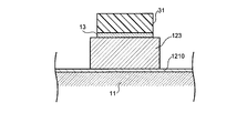
- a seed layer 1210 is formed on the first surface 11a, the second surface 11b of the substrate 11, and the inner surface 15a of the through hole 15 by an electroless plating method.
- the adhesion layer may be formed before forming the seed layer 1210.
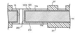
- a resist layer 31 is formed on a part of the seed layer 1210.
- a conductive layer is formed on a portion of the seed layer 1210 exposed from the resist layer 31 by an electrolytic plating method.
- the first upper conductive layer 123 is formed on the first surface 11a side
- the inner peripheral portion 203 is formed on the through hole 15
- the fourth upper conductive layer 213 is formed on the second surface 11b side.
- the resist layer 31 is removed.
- the first insulating layer 13 is formed, and at this time, the exposed portion of the seed layer 1210 is removed. Thereby, the respective conductive layers are separated, and the first conductive layer 12 is formed on the first surface 11a side, the third conductive layer 20 is formed on the through hole 15, and the fourth conductive layer 21 is formed on the second surface 11b side. . Subsequently, as shown in FIG. 9, a second conductive layer 14 is formed on the first insulating layer 13.
- a capacitor including the first conductive layer 12, the first insulating layer 13 on the first conductive layer 12, and the second conductive layer 14 on the first insulating layer 13 can be configured. Regarding the manufacturing method from FIG. 7 to FIG. 9, details of the manufacturing method of the portion to be the capacitor 100 will be described later.
- the second insulating layer 22 is formed, the via hole 23 is formed, and the connection portion 24 is formed, whereby the configuration shown in FIG. 2 is realized.
- the thickness of the second insulating layer 22 (the distance from the first surface 11a of the substrate 11 to the surface of the second insulating layer 22 in the example of FIG. 2) is such that unevenness of the capacitor 100 and the like is flattened on the surface. It is preferable that the thickness be in the range of not less than the thickness of the structure in which the first conductive layer 12, the first insulating layer 13 and the second conductive layer 14 are laminated, and not more than twice the thickness. In the vicinity of the capacitor 100, a capacitance component is generated between the first conductive layer 12 and the connection portion 24.
- the second insulating layer 22 having a lower relative dielectric constant than the first insulating layer 13 be formed thick between the first conductive layer 12 and the connection portion 24.
- the distance from the surface of the first insulating layer 13 to the surface of the second insulating layer 22 is preferably, for example, 10 times or more the thickness of the first insulating layer 13. .
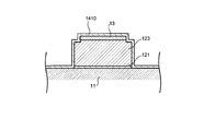
- FIGS. 10 to 15 are diagrams illustrating a method of manufacturing the capacitor according to the first embodiment of the present disclosure.
- 10 to 15 each show a cross-sectional shape (a cross-sectional view taken along line BB of FIG. 1) of a portion corresponding to FIG.
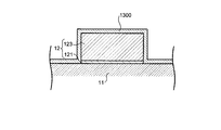
- an insulating layer 1300 is formed to cover the first upper conductive layer 123 from the state shown in FIG.
- a surface treatment of exposing the surface including the first upper conductive layer 123 to plasma such as NH3 plasma may be performed. Accordingly, the oxide on the surface of the first upper conductive layer 123 may be removed, and the adhesion between the first upper conductive layer 123 and the insulating layer 1300 may be increased.
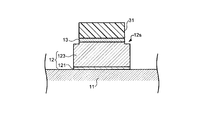
- a resist layer 31 is formed, and a portion of the insulating layer 1300 that is not covered with the resist layer 31 is removed, and a first insulating layer 13 is formed as shown in FIG. After that, the resist layer 31 is removed.
- the resist layer 31 may be formed in a portion other than the portion where the first insulating layer 13 is formed.
- the first insulating layer 13 may be formed by removing a part of the insulating layer 1300 by removing the resist layer 31 by wet etching.
- a part of the first upper conductive layer 123 that is exposed from the first insulating layer 13 is removed to form a step 12s.
- the seed layer 1210 exposed from the first upper conductive layer 123 is also removed. That is, of the first conductive layer 12, the upper surface 12-2u of the second portion 12-2 is formed outside the boundary 12-1p.
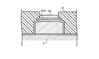
- a seed layer 1410 is formed.
- a resist layer 31 is formed on a part of the seed layer 1410, and a conductive layer is formed on a part of the seed layer 1410 exposed from the resist layer 31 by an electrolytic plating method.
- a second upper conductive layer 143 is formed.
- the resist layer 31 is removed.
- the capacitor 100 shown in FIG. 9 is realized by removing the seed layer 1410 other than the portion covered by the second upper conductive layer 143.
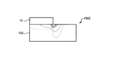
- FIG. 16 is a diagram illustrating the stress distribution of the first conductive layer of the capacitor in the comparative example.
- FIG. 17 is a diagram illustrating the stress distribution of the first conductive layer of the capacitor according to the first embodiment of the present disclosure. 16 and 17 show the distribution of stress applied to the first insulating layer 13 in the first conductive layer, and the distribution is shown by contour lines. FIGS. 16 and 17 show that the contour lines having the same contour type have the same magnitude of stress. Further, the line type indicates that the stress increases in the order of a dotted line, a broken line, and a solid line. When FIG. 16 is compared with FIG. 17, a result is obtained in which the stress is reduced by the presence of the step 12s in the capacitor 100 shown in FIG.
- the method for manufacturing the capacitor 100 is not limited to the method described above. An example of another manufacturing method will be described.
- FIGS. 18 and 19 are diagrams illustrating another method of manufacturing the capacitor according to the first embodiment of the present disclosure.
- the timing at which the seed layer 1210 is removed is different from the above-described example.
- the seed layer 1210 other than the portion covered with the first upper conductive layer 123 is removed to form the first lower conductive layer 121, and then the first conductive layer An insulating layer 1300 is formed so as to cover 12.
- a resist layer 31 is formed, a portion of the insulating layer 1300 that is not covered with the resist layer 31 is removed, and a first insulating layer 13 is formed as shown in FIG.
- a portion of the first upper conductive layer 123 that is exposed from the first insulating layer 13 is removed to form a step 12s.
- This also forms capacitor 100 having a structure similar to that of FIG.
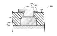
- ⁇ Second embodiment> an example of the capacitor 100A in which the second conductive layer 14 of the capacitor 100 in the first embodiment is shared with the connection unit 24 will be described.
- the capacitor 100A has a structure shown in FIG. 23, and a method for manufacturing the capacitor 100A will be described with reference to FIGS.
- FIGS. 20 to 23 are diagrams illustrating a method of manufacturing the capacitor according to the second embodiment of the present disclosure.
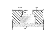
- a second insulating layer 22A including an opening 22Ah is formed.
- the opening 22Ah is formed at the same time as the via hole 23 shown in FIG. 2 and has a similar structure, except that the opening 22Ah is formed so as to expose a part of the first insulating layer 13.
- a seed layer 1410A is formed.
- the seed layer 1410A is formed to cover the first insulating layer 13 and the second insulating layer 22A. As shown in FIG.
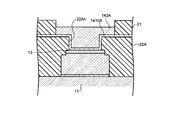
- a resist layer 31 is formed, and a second upper conductive layer 143A is formed by an electrolytic plating method.
- the resist layer 31 is removed, and the seed layer 1410A other than the portion covered with the second upper conductive layer 143A is removed, thereby forming the second lower conductive layer 141A.
- the second conductive layer 14A thus formed is formed together with the connection part 24. Note that the opening 22Ah and the via hole 23 may be formed at different timings. Further, the second conductive layer 14A and the connection portion 24 may be formed at different timings.
- the second conductive layer 14A contacts the inner surface of the opening 22Ah. Further, a second insulating layer 22A is arranged in a part between the second conductive layer 14A and the first insulating layer 13. That is, a part of the second conductive layer 14A is in contact with a part of the first insulating layer 13.
- the second portion 12-2 is arranged so as to surround the first portion 12-1 of the first conductive layer 12. That is, the entire edge of the first insulating layer 13 was disposed on the first conductive layer 12.
- a capacitor in which at least a part of the edge of the first insulating layer 13 is disposed outside the first conductive layer 12 will be described.
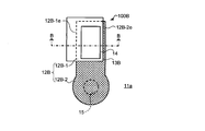
- FIG. 24 is a schematic plan view illustrating an interposer according to the third embodiment of the present disclosure.
- FIG. 25 is a schematic cross-sectional view (a cross-sectional view taken along the line BB of FIG. 24) illustrating a capacitor included in the interposer according to the third embodiment of the present disclosure.
- the first conductive layer 12 in the first embodiment surrounds the periphery of the first portion 12-1, so that the edge of the second portion 12-2 (the side surface 12-1 shown in FIG. 4). 2e) and the edge of the first conductive layer 12 were common.
- the first insulating layer 13B covers the upper surface 12B-1u, covers the side surfaces 12B-1e, and further covers a part of the first surface 11a of the substrate 11.
- the step 12Bs exists at the end.
- the stress applied to the first insulating layer 13B from the first conductive layer 12B is reduced.
- stress does not concentrate in a region where the end of the first insulating layer 13B does not exist on the first conductive layer 12B, so that the first insulating layer 13B is less likely to crack on the first conductive layer 12B. .
- the thickness of the portion of the first insulating layer 13B that covers the side surfaces 12B-1e may be smaller than the thickness of the portion that covers the upper surface 12B-1u. At this time, even if the thickness of the first insulating layer 13B at the portion covering the side surfaces 12B-1e is 30% or more and 90% or less with respect to the thickness of the first insulating layer 13B at the portion covering the upper surface 12B-1u. It may be 60% or more and 80% or less.
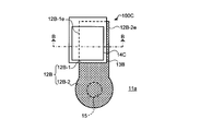
- FIG. 26 is a schematic plan view showing an interposer according to the fourth embodiment of the present disclosure.
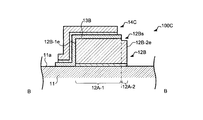
- FIG. 27 is a schematic cross-sectional view (a cross-sectional view taken along the line BB of FIG. 26) illustrating a capacitor included in the interposer according to the fourth embodiment of the present disclosure.
- second conductive layer 14C is formed along the arrangement of first insulating layer 13B. Therefore, the first insulating layer 13B has a region sandwiched between the second conductive layer 14C and the side surface 12B-1e of the first portion 12B-1, and is further sandwiched between the second conductive layer 14C and the substrate 11. It also has an area.
- a plurality of capacitors 100C in which a part of the second conductive layer 14C extends outside the first conductive layer 12B as in the above-described fourth embodiment are connected via the second conductive layer 14C. Will be described.
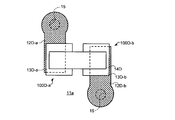
- FIG. 28 is a schematic plan view showing an interposer according to the fifth embodiment of the present disclosure.
- the first capacitor 100Da and the second capacitor 100Db in the fifth embodiment each have a configuration similar to the capacitor 100C in the fourth embodiment.
- the first capacitor 100Da includes a first conductive layer 12Da, a first insulating layer 13Da, and a second conductive layer 14D.
- the second capacitor 100D-b includes a first conductive layer 12D-b, a first insulating layer 13D-b, and a second conductive layer 14D.
- the second conductive layer 14D is arranged as a common electrode in the first capacitor 100Da and the second capacitor 100Db.
- the first capacitor 100D-a and the second capacitor 100D-b are arranged rotationally symmetric in this example, but may be arranged line-symmetrically or in a form without symmetry. Good. In any case, it is assumed that the first capacitor 100Da and the second capacitor 100Db are adjacent to each other.
- the first conductive layer 12D-a and the first conductive layer 12D-b are separated from each other. Further, the first insulating layer 13D-a and the first insulating layer 13D-b are separated from each other.
- the second conductive layer 14D is in contact with the first surface 11a of the substrate 11 in a region other than the region in contact with the first insulating layers 13D-a and 13D-b.
- FIG. 29 is a schematic plan view showing an interposer according to the sixth embodiment of the present disclosure.
- the first capacitor 100E-a and the second capacitor 100E-b in the sixth embodiment have a configuration similar to the first capacitor 100D-a and the second capacitor 100D-b in the fifth embodiment, respectively.
- the first capacitor 100E-a includes a first conductive layer 12E-a, a first insulating layer 13E, and a second conductive layer 14E.
- the second capacitor 100E-b includes a first conductive layer 12E-b, a first insulating layer 13E, and a second conductive layer 14E.
- the first insulating layer 13E is arranged as a common insulating layer in the first capacitor 100Ea and the second capacitor 100E-b.
- the second conductive layer 14E is arranged as a common electrode in the first capacitor 100E-a and the second capacitor 100E-b.
- the first capacitor 100E-a and the second capacitor 100E-b are arranged rotationally symmetric in this example, but may be arranged line-symmetrically or in a form without symmetry. Good. In any case, it is assumed that the first capacitor 100Ea and the second capacitor 100Eb are adjacent to each other.
- the first conductive layer 12E-a and the first conductive layer 12E-b are separated from each other.
- the second conductive layer is arranged as a common electrode in a plurality of capacitors, but in the seventh embodiment, the first conductive layer is arranged in a common electrode in a plurality of capacitors.
- FIG. 30 is a schematic plan view showing the interposer according to the seventh embodiment of the present disclosure.
- FIG. 31 is a schematic cross-sectional view (a cross-sectional view taken along the line CC of FIG. 30) illustrating the capacitor according to the seventh embodiment of the present disclosure.
- a part of the configuration including a portion corresponding to a capacitor is described, and other configurations are omitted.
- the first capacitor 100Fa and the second capacitor 100Fb in the seventh embodiment each have a configuration similar to the capacitor 100 in the first embodiment.
- a step 12Fs is formed around the area of the first capacitor 100F-a and the area of the second capacitor 100F-b (the area corresponding to the first portion 12F-1).
- the region other than -a and the second capacitor 100F-b (the region corresponding to the second portion 12F-2) is thinner.
- one of the two first portions 12F-1 is defined as the third portion 12F-3 as shown in FIG. 31, the following can be paraphrased as follows.
- the second portion 12F-2 is adjacent to the first portion 12F-1 and the third portion 12F-3.
- the first portion 12F-1 and the third portion 12F-3 are separated via the second portion 12F-2.
- the first capacitor 100F-a includes a first conductive layer 12F, a first insulating layer 13F-a, and a second conductive layer 14F-a.
- the second conductive layer 14F-a is disposed on the opposite side of the first insulating layer 13F-a from the first portion 12F-1.
- the second capacitor 100F-b includes a first conductive layer 12F, a first insulating layer 13F-b, and a second conductive layer 14F-b.
- the second conductive layer 14F-b is disposed on the opposite side of the first insulating layer 13F-b from the third portion 12F-3.
- the first conductive layer 12F is arranged as a common electrode in the first capacitor 100F-a and the second capacitor 100F-b.
- the first insulating layer 13F-a and the first insulating layer 13F-b may be continuously arranged as a common insulating layer (referred to as a first insulating layer 13F).
- the region where the first insulating layer 13F exists is a region corresponding to the first portion 12F-1, the second portion 12F-2, and the third portion 12F-3.
- the thickness of the second portion 12F-2 is different from the thickness shown in FIG. 31, and is the same as the thickness of the first portion 12F-1 and the third portion 12F-3.
- the continuous 12th step is not provided at the boundary between the second portion 12F-2 and the first portion 12F-1 and at the boundary between the second portion 12F-2 and the third portion 12F-3.
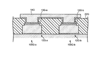
- FIG. 32 is a schematic cross-sectional view illustrating a capacitor according to the eighth embodiment of the present disclosure.
- the first capacitor 100G-a and the second capacitor 100G-b each have a configuration similar to the capacitor 100A in the second embodiment.
- the first capacitor 100G-a includes a first conductive layer 12G-a, a first insulating layer 13G-a, and a second conductive layer 14G.
- the second capacitor 100G-b includes a first conductive layer 12G-b, a first insulating layer 13G-b, and a second conductive layer 14G.
- the second conductive layer 14G is arranged as a common electrode via a portion arranged on the second insulating layer 22G in the first capacitor 100G-a and the second capacitor 100G-b.
- a structure in which the first capacitor 100G-a and the second capacitor 100G-b are connected in series using the first conductive layer 12G-a and the first conductive layer 12G-b as terminals can be realized.
- the first conductive layer 12G-a and the first conductive layer 12G-b are electrically connected to form one wiring
- the second conductive layer 14G is connected to the first capacitor 100G-a and the second capacitor 100G.
- the series connection can be realized by dividing each of -b. In this case, a series connection structure similar to the configuration of the seventh embodiment shown in FIG. 31 may be used.
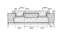
- FIG. 33 is a schematic cross-sectional view illustrating a capacitor according to the ninth embodiment of the present disclosure.
- the first capacitor 100H-a includes a first conductive layer 12H, a first insulating layer 13H-a, and a second conductive layer 14H.
- the second capacitor 100H-b includes a first conductive layer 12H, a first insulating layer 13H-b, and a second conductive layer 14H.
- the first conductive layer 12H is arranged as a common electrode in the first capacitor 100Ha and the second capacitor 100Hb.
- the second conductive layer 14G is disposed as a common electrode via a portion disposed on the second insulating layer 22G in the first capacitor 100Ha and the second capacitor 100Hb.
- the first capacitor 100Ha and the second capacitor 100Hb are in a state where a plurality of capacitors are connected in parallel. Therefore, the two capacitors can be formed integrally without being separated.
- the first insulating layer 13G-a and the first insulating layer 13G-b are separated from each other to reduce the size of the integrated insulating layer, and as a result, the first conductive layer is formed between them.
- the second portion 12H-2 of the layer 12H is formed. Thereby, a step is formed at the boundary between the first portion 12H-1 and the second portion 12H-2, and the stress on the first insulating layers 13G-a and 13G-b can be reduced.
- the idea of reducing the size of the integral insulating layer as described above also applies to the structure in which the first conductive layer 12G-a and the first conductive layer 12G-b described in the eighth embodiment are integrated. The same can be applied.
- ⁇ Tenth embodiment> In the tenth embodiment, an example in which the first conductive layer has a stacked structure different from that of the first embodiment will be described.
- the first conductive layer 12 in the first embodiment and the first conductive layer 12J in the tenth embodiment will be described while comparing the side surface shapes near the first surface 11a of the substrate 11.
- FIG. 34 is a schematic cross-sectional view illustrating a side surface shape of the first conductive layer according to the first embodiment of the present disclosure.
- the first conductive layer 12 in the first embodiment has a structure in which the first lower conductive layer 121 and the first upper conductive layer 123 are stacked as described above.
- the first lower conductive layer 121 is Cu formed by an electroless plating method
- the first upper conductive layer 123 is Cu formed by an electrolytic plating method.
- both the first lower conductive layer 121 and the first upper conductive layer 123 are made of Cu, but the former is formed by an electroless plating method, and the latter is formed by an electrolytic plating method. Even so, the etching rate can be different. Accordingly, when forming the first lower conductive layer 121 by removing the seed layer 1210, the first lower conductive layer 121 can accelerate the etching more quickly than the first upper conductive layer 123. As a result, the etching proceeds from below the first upper conductive layer 123, and the depression 12d can be formed on the side surface 12-2e.
- the second insulating layer 22 By forming the second insulating layer 22 along such a depression 12d, it is possible to enhance the adhesion.
- the shape of the depression 12d can be variously changed by controlling the combination of the laminated structures, for example, the film thickness, the film quality, and the like.
- FIG. 35 is a schematic cross-sectional view illustrating a side surface shape of the first conductive layer according to the tenth embodiment of the present disclosure.
- the first conductive layer 12J shown in FIG. 35 has a structure in which a first lower conductive layer 121J and a first upper conductive layer 123 are stacked.
- the first lower conductive layer 121J has a structure in which a sputtered Ti layer 1211, a sputtered Cu layer 1213, and a vapor-deposited Cu layer 1215 are stacked.
- dents 1211b, 121Jd, and 12Jd are formed on the side surfaces 12H-2e by etching when the first lower conductive layer 121J is formed from the seed layer.
- the etching rate can be different depending on the difference in their formation methods. Depressions 121Jd and 12Jd can be generated in 12H-2e.
- the material of the recess 1211b is different between the sputtered Ti layer 1211 and the upper layer Cu, etching from below the sputtered Cu layer 1213 hardly proceeds. Therefore, the lower surface of the sputtered Cu layer 1213 is substantially parallel to the first surface 11a of the substrate 11.
- Such a depression 1211b may be filled with the second insulating layer 22, or a space may be partially formed.
- FIG. 36 is a schematic plan view showing the interposer according to the eleventh embodiment of the present disclosure. More specifically, FIG. 36 shows the interposer 10 manufactured by the method described in the first embodiment. In this figure, many components are omitted for the sake of simplicity.
- the capacitor 100 a part of the first insulating layer 13 and the second conductive layer 14 formed on the first surface 11a side of the substrate 11 Only shows.
- a second insulating layer 22 is formed so as to cover the capacitor 100.
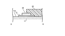
- an annular conductive layer 29 and the first insulating layer 13 are formed along the end of the second insulating layer 22.
- FIG. 37 is a schematic cross-sectional view (a cross-sectional view taken along line DD of FIG. 36) showing the annular conductive layer 29 included in the interposer according to the eleventh embodiment of the present disclosure.
- the conductive layer 29 is annularly disposed along the first insulating layer 13 on the first insulating layer 13 formed in an annular shape.
- the width of first insulating layer 13 is larger than the width of conductive layer 29.
- the conductive layer 29 is formed, for example, simultaneously with the step of forming the second conductive layer 14.
- an annular conductive layer 29 is also formed on the first insulating layer 13 along a position where the edge of the second insulating layer 22 is to be formed.
- the first insulating layer 13 wider than the conductive layer 29 is disposed between the conductive layer 29 and the substrate 11 at the position of the end of the second insulating layer 22.
- the adhesion at the end of the second insulating layer 22 is improved by the first insulating layer 13.
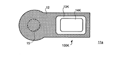
- FIG. 38 is a schematic sectional view showing a capacitor according to the twelfth embodiment of the present disclosure.
- the corners of the first insulating layer 13K and the second conductive layer 14K have a round shape. Since the corners of the first insulating layer 13K have a round shape as described above, the stress applied to the corners of the first insulating layer 13K can be further reduced. Similarly, the stress applied to the corners of the second conductive layer 14K can be reduced. Thereby, it is possible to prevent the first insulating layer 13K and the second conductive layer 14K from peeling off from the lower layer.
- one corner of the first insulating layer 13K and the second conductive layer 14K may not have a round shape. Further, any one of the plurality of corners may not have a round shape, and any shape may be different from other shapes.
- the radius of curvature is preferably 5 ⁇ m or more. On the other hand, if it is less than 30 ⁇ m, the radius of curvature may be even smaller.
- FIG. 39 is a schematic plan view illustrating capacitors and inductors included in the interposer according to the thirteenth embodiment of the present disclosure.
- This schematic plan view is a plan view showing the first conductive layer 12L on the first surface 11a side of the substrate 11.
- some components such as the connection unit 24 are omitted.
- FIG. 40 is a schematic cross-sectional view (a cross-sectional view taken along the line EE of FIG. 39) illustrating the interposer according to the thirteenth embodiment of the present disclosure.
- the interposer 10L may include at least the inductor 27 and the capacitor 100L.
- the interposer 10L has at least a third conductive layer 20a electrically connected to the first conductive layer 12L and a plurality of third conductive layers 20b forming the inductor 27.
- the third conductive layer 20a is formed in a through hole 15-1 between the inductor 27 and the capacitor 100L (the first conductive layer 12L, the first insulating layer 13L, and the second conductive layer 14L).
- the plurality of third conductive layers 20b are formed in each of the plurality of through holes 15-2 in a region (a range included in a dotted line) configuring the inductor 27.
- first conductive layer 12L on first surface 11a side of substrate 11 forms inductor 27, and another part of first conductive layer 12L forms a lower electrode of capacitor 100L.
- the thickness Th1 of the first conductive layer 12L forming the inductor 27 is the thickness outside (corresponding to the second portion) of the first conductive layer 12L forming the lower electrode of the capacitor 100L. It may be substantially the same as Th2. In addition, when the thickness of both satisfies the following relationship, it can be regarded as substantially the same. ⁇ 10% ⁇ (Th1-Th2) / Th1 ⁇ + 10%
- ⁇ Th1 may be 0.5 ⁇ m or more and 30 ⁇ m or less, but more preferably 5 ⁇ m to 20 ⁇ m. This is because the performance of the inductor 27 is improved.
- the thickness of the third conductive layers 20a and 20b may be not less than 50% and not more than 100% of Th1 on the first surface 11a of the substrate 11.
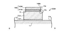
- FIG. 41 is a schematic sectional view showing a capacitor according to a fourteenth embodiment of the present disclosure.
- the fact that the side surface 13e and the side surface 14Me are aligned is not limited to the case where they are completely matched, but also includes the case where they are substantially matched.
- Substantially matching means for example, that d1 may be d2 or less, d1 may be 0.1 ⁇ m or less, and d1 is 1% or less of the thickness of the second conductive layer 14M. Alternatively, d1 may be 50% or less of the thickness of the first insulating layer 13.
- the end surface of the second conductive layer 14M is not formed on the first insulating layer 13, so that stress is concentrated. It is possible to prevent a portion to be formed on the first insulating layer 13. Therefore, cracks in the first insulating layer 13 can be suppressed, and peeling between the first insulating layer 13 and the second conductive layer 14M can be suppressed.
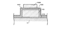
- FIG. 42 is a diagram illustrating a method for manufacturing the capacitor according to the fourteenth embodiment of the present disclosure.
- a seed layer 1410 is formed so as to cover the insulating layer 1300, and a second upper conductive layer 143M is formed in the same manner as in the first embodiment.
- FIG. 43 is a diagram illustrating a method for manufacturing the capacitor according to the fourteenth embodiment of the present disclosure.
- the second lower conductive layer 141M and the first insulating layer 13 are formed by removing the seed layer 1410 and the insulating layer 1300 other than the portion covered by the second upper conductive layer 143M.
- a part of the first upper conductive layer 123 that is exposed from the first insulating layer 13 is removed to form a step 12s.
- the seed layer 1210 exposed from the first upper conductive layer 123 is also removed.
- capacitor 100M shown in FIG. 41 is realized.
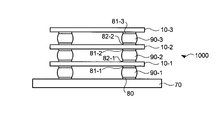
- FIG. 44 is a diagram illustrating a semiconductor device according to a fifteenth embodiment of the present disclosure.
- the semiconductor device 1000 has three stacked interposers 10 (10-1, 10-2, 10-3) and is connected to the LSI substrate 70.
- the interposer 10-1 has a semiconductor element such as a DRAM, for example, and has connection terminals 81-1 and 82-1 formed by the connection section 24 and the like. These interposers 10 (10-1, 10-2, 10-3) do not need to use a glass substrate, and some of the interposers 10 use a substrate made of a different material from other interposers 10. It may be something.
- the connection terminal 81-1 is connected to the connection terminal 80 of the LSI substrate 70 via a bump 90-1.
- connection terminal 82-1 is connected to the connection terminal 81-2 of the interposer 10-2 via the bump 90-2.
- the connection terminal 82-2 of the interposer 10-2 and the connection terminal 83-1 of the interposer 10-3 are also connected via the bump 90-3.
- the bumps 90 (90-1, 90-2, 90-3) use, for example, metals such as indium, copper, and gold.
- the number of layers is not limited to three, but may be two, or may be four or more.
- the connection between the interposer 10 and another substrate is not limited to the method using a bump, and another bonding technique such as eutectic bonding may be used.
- the interposer 10 and another substrate may be bonded by applying and baking a polyimide, an epoxy resin, or the like.
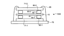
- FIG. 45 is a diagram illustrating another example of the semiconductor device according to the fifteenth embodiment of the present disclosure.
- a semiconductor device 1000 shown in FIG. 45 has a stacked structure in which semiconductor circuit boards (semiconductor chips) 71-1 and 71-2 such as a MEMS device, a CPU, and a memory, and an interposer 10 are stacked, and is connected to an LSI substrate 70. Have been.
- the interposer 10 is disposed between the semiconductor circuit board 71-1 and the semiconductor circuit board 71-2, and is connected to each other via bumps 90-1 and 90-2.
- the semiconductor circuit board 71-1 is mounted on the LSI board 70.
- the LSI board 70 and the semiconductor circuit board 71-2 are connected by wires 95.
- the interposer 10 is used as an interposer for stacking a plurality of semiconductor circuit boards and three-dimensionally mounting them.
- a multifunctional semiconductor device can be realized. For example, by using the semiconductor circuit board 71-1 as a three-axis acceleration sensor and the semiconductor circuit board 71-2 as a two-axis magnetic sensor, a semiconductor device in which a five-axis motion sensor is realized by one module can be realized. .
- a sensing result may be output as an analog signal.
- a low-pass filter, an amplifier, and the like may be formed on the semiconductor circuit board or the interposer 10.
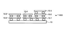
- FIG. 46 is a diagram illustrating still another example of the semiconductor device according to the fifteenth embodiment of the present disclosure.
- FIG. 46 is a diagram illustrating still another example of the semiconductor device according to the fifteenth embodiment of the present disclosure.
- the above two examples are three-dimensional mounting, this example is an example applied to 2.5-dimensional mounting.
- six interposers 10 (10-1 to 10-6) are stacked and connected to the LSI substrate 70.
- the interposers 10 are stacked and connected to the LSI substrate 70.
- the interposers 10-1 and 10-5 are connected on the LSI substrate 70, the interposers 10-2 and 10-4 are connected on the interposer 10-1, and the interposers 10- and 10-4 are connected on the interposer 10-2. 3 is connected, and the interposer 10-6 is connected on the interposer 10-5.
- the interposers 10-3, 10-4, 10-6, etc. may be replaced with semiconductor circuit boards.
- the semiconductor device 1000 manufactured as described above is mounted on various electronic devices such as a mobile terminal, an information processing device, and a home appliance.
- the mobile terminal includes a mobile phone, a smartphone, a notebook personal computer, and the like.
- the information processing device includes a desktop personal computer, a server, a car navigation, and the like.
- the electronic device include, for example, a wireless local area network (LAN) device, a set-top box, a music player, a video player, an entertainment unit, a navigation device, a communication device, a personal digital assistant (PDA), and a fixed position data unit. It may be.
- LAN wireless local area network
- PDA personal digital assistant
- FIG. 47 is a diagram illustrating an example of an electronic apparatus using the semiconductor device according to the fifteenth embodiment of the present disclosure.
- a smartphone 500 and a notebook personal computer 600 are shown.
- These electronic devices have a control unit 1100 including a CPU or the like that executes an application program to realize various functions.
- the various functions include a function of using an output signal from the semiconductor device 1000.
- the semiconductor device 1000 may have the function of the control unit 1100.
- the present disclosure is not limited to the embodiments described above, and includes various other modifications.
- the above-described embodiments have been described in detail for easy understanding of the present disclosure, and are not necessarily limited to those having all the configurations described above.
- a part of the configuration of one embodiment may be replaced with the configuration of another embodiment, and the configuration of one embodiment may be added to the configuration of another embodiment.
- some modifications will be described.
- about the example which changed 1st Embodiment it can be applied also as an example which changes other embodiment.
- Each of the first conductive layer 12 and the second conductive layer 14 has a laminated structure including a seed layer and a conductive layer formed by an electrolytic plating method.
- the conductive layer formed by another method is used. It may be. That is, at least one or both of the first conductive layer 12 and the second conductive layer 14 may have a single-layer structure.
- a vapor deposition method including chemical vapor deposition (CVD) and physical vapor deposition (PVD) is exemplified.
- the chemical vapor deposition include plasma CVD and atomic layer deposition (ALD).
- the physical vapor deposition include sputtering and vacuum vapor deposition. Further, it may be formed by etching a metal foil or by applying a conductive paste such as a metal nanopaste.
- the first insulating layer 13 may be formed by an evaporation method including chemical vapor deposition (CVD) and physical vapor deposition (PVD).
- a desired pattern may be formed on the conductive layer and the insulating layer by photolithography, or may be planarized by etch back or chemical mechanical polishing (CMP).
- the material of the first conductive layer 12 and the second conductive layer 14 is not limited to Cu, but may be gold (Au), silver (Ag), copper (Cu), iron (Fe), nickel (Ni), platinum ( A material having conductivity such as Pt), palladium (Pd), ruthenium (Ru), and tungsten (W) may be included.
- the second insulating layer 22 is an organic material, but may be an inorganic material, or may have a laminated structure of an inorganic material insulating layer and an organic material insulating layer.
- the first insulating layer 13 may be disposed not only in the portion configuring the capacitor 100 but also as the first insulating layer 13 other than the portion configuring the capacitor 100. At this time, the portion of the first insulating layer 13 constituting the capacitor 100 and the other portion of the first insulating layer 13 may be separated from each other or may be continuous.
- the first insulating layer 13 other than the portion constituting the capacitor 100 may be formed, for example, so as to cover at least a part of the third conductive layer 20 of the through hole 15.
- the seed layer is removed by etching after forming the first insulating layer 13, a portion of the third conductive layer 20, particularly, the conductive layer (first The boundary portion between the conductive layer 12 and the third conductive layer 20) is protected by the first insulating layer 13, so that the protected portion of the conductive layer can be prevented from becoming thin.
- the third conductive layer 20 formed inside the through hole 15 is formed along the inner side surface 15 a of the through hole 15 and is arranged so as not to close the through hole 15. At least one of the first surface 11a side and the second surface 11b side may be arranged to be closed, or the whole of the through hole 15 may be arranged to be closed. When the entire through hole 15 is closed, it can be said that the third conductive layer 20 is formed so as to fill the through hole 15 in other words.
- the capacitor 100L and the inductor 27 are connected by the third conductive layer 20a.
- the third conductive layer 20a is deformed so as to be closed at least in the vicinity of the first surface 11a in the through-hole 15-1, the conductive layer closing the through-hole 15-1 is removed from the first conductive layer 12L.
- the capacitor 100L may be formed directly above the through hole 15-1.
- the capacitor 100 is disposed on the interposer 10 described above.
- the capacitor 100 may be disposed on the interposer 10 including a through electrode such as the third conductive layer 20. It is not limited to the case where it is applied.
- a wiring board may not include a through electrode.
- the conductive layer may be arranged only on the first surface 11a side of the substrate 11.
- the substrate on which the capacitor 100 is disposed is not limited to a substrate applied to an application as an interposer disposed between a circuit substrate and a semiconductor chip, even when the substrate includes a through electrode. You may apply to the use as a penetration electrode board
- the penetrating electrode substrate includes not only an interposer disposed between a circuit substrate and a semiconductor chip or the like, but also an IPD (Integrated Passive Device) without a semiconductor chip or the like.
- IPD Integrated Passive Device
- the semiconductor chip and the like may be arranged on the circuit board at a different position from the through electrode substrate and may be electrically connected to the circuit board.
- the respective materials are determined such that the thermal expansion coefficient of the second lower conductive layer 141 is between the thermal expansion coefficient of the first insulating layer 13 and the thermal expansion coefficient of the second upper conductive layer 143. May be.
- the second upper conductive layer 143 is formed of Cu having a thermal expansion coefficient of 16.8 ppm / K and the first insulating layer 13 is formed of 3.25 ppm / K of silicon nitride
- the second lower conductive layer is formed.
- 141 from Ti (8.4 ppm / K), Cr (8.2 ppm / K), Ni (13.4 ppm / K), or the like, the stress can be further reduced.
- the second lower conductive layer 141 is formed of a plurality of films, the closer to the first insulating layer 13, the closer to the first insulating layer 13 the thermal expansion coefficient is, and the closer to the second upper conductive layer 143. It is preferable that the second upper conductive layer 143 be formed with a film having a closer thermal expansion coefficient.
- a second lower conductive layer 141 in which a Ni film is stacked on the second upper conductive layer 143 (Cu) side and a Ti or Cr film is stacked on the first insulating layer 13 (silicon nitride) side may be formed.
- Reference Signs List 10 interposer 11 substrate, 11a first surface, 11b second surface, 12 first conductive layer, 12-1 first portion, 12-1p boundary, 12-1u upper surface, 12-2 ... Second portion, 12-2e side surface, 12-2u upper surface, 12s step, 13 second insulating layer, 14 second conductive layer, 14e side surface, 15 through hole, 15a inner side surface, 20 ... third conductive layer, 21 ... fourth conductive layer, 22 ... second insulating layer, 22Ah ... opening, 23 ... via hole, 24 ... connecting part, 25 ... ball, 27 ... inductor, 29 ... conductive layer, 31 ...
- resist layer 40 circuit board, 50 semiconductor chip, 70 board, 71 semiconductor circuit board, 80 connection terminal, 90 bump, 95 wire, 100 capacitor, 121 first lower conductive layer, 123 first Upper conductive layer, 141... Second lower conductive layer, 14 ... Second upper conductive layer, 201 outer peripheral part, 203 inner peripheral part, 211 fourth lower conductive layer, 213 fourth upper conductive layer, 500 smartphone, notebook personal computer, 1000 semiconductor device, 1100: control unit, 1210: seed layer, 1211: sputtered Ti layer, 1213: sputtered Cu layer, 1215: evaporated Cu layer, 1300: insulating layer, 1410: seed layer
Landscapes
- Engineering & Computer Science (AREA)
- Microelectronics & Electronic Packaging (AREA)
- Manufacturing & Machinery (AREA)
- Production Of Multi-Layered Print Wiring Board (AREA)
- Power Engineering (AREA)
- Parts Printed On Printed Circuit Boards (AREA)
- Semiconductor Integrated Circuits (AREA)
- Internal Circuitry In Semiconductor Integrated Circuit Devices (AREA)
- Structure Of Printed Boards (AREA)
Abstract
本開示の配線基板によれば、絶縁表面を有する基板と、前記基板上に配置された第1導電層であって、第1厚さを有する第1部分および当該第1厚さよりも薄い第2厚さを有し当該第1部分に隣接する第2部分を含む第1導電層と、前記第2部分から離隔して前記第1部分上に配置された第1絶縁層と、前記第1絶縁層に対して前記第1部分とは反対側に配置された第2導電層と、を備える。
Description
本開示は、配線基板に関する。
配線付の基板上にMIM(Metal-Insulator-Metal)キャパシタが形成される場合がある。このキャパシタは、導電層によって絶縁層を挟んだ構造を有する。導電層と絶縁層とは、熱膨張係数に違いがある。したがって、製造プロセスなどによる熱履歴に応じた伸縮によって、応力が生じる。伝送抵抗を小さくするために配線を厚くすると、この現象はさらに顕著になる。この応力を絶縁層が受けると、その応力を緩和するために絶縁層が導電層から剥離したり、絶縁層にクラックが生じたりする。このように、大きな応力の発生はキャパシタの信頼性を低下させる要因となる。特許文献1には、応力緩和のため、絶縁層が弾性体である技術が開示されている。この弾性体は有機材料である。
有機材料は、一般的に誘電正接が大きい。そのため、導電層に高周波信号を印加した場合には、大きな伝送損失が生じて電力効率が悪化する。電力の損失が熱に変換されると、その熱は、素子特性の低下および熱雑音による信号品質の低下など、素子の性能を悪化させる。このように、特許文献1に開示された構造では、応力の緩和ができたとしても、素子の性能を低下させることになる。
本開示の目的の一つは、キャパシタの信頼性を向上することにある。
本開示によれば、絶縁表面を有する基板と、前記基板上に配置された第1導電層であって、第1厚さを有する第1部分および当該第1厚さよりも薄い第2厚さを有し当該第1部分に隣接する第2部分を含む第1導電層と、前記第2部分から離隔して前記第1部分上に配置された第1絶縁層と、前記第1絶縁層に対して前記第1部分とは反対側に配置された第2導電層と、を備える、配線基板が提供される。
前記第1部分および前記第2部分は、前記第1絶縁層側において同一材料で形成された領域を含んでもよい。
前記第1導電層は、第1膜および当該第1膜とは膜質が異なる第2膜を含み、前記第2膜は、前記第1膜と前記第1絶縁層とに挟まれて配置され、前記第2部分における前記第2膜は、前記第1部分における前記第2膜よりも薄くてもよい。
前記第2導電層は、前記第1絶縁層の縁部のうち前記第2部分側に対応する第1縁部から離隔して配置されてもよい。
前記基板の表面の法線方向に沿って見た場合において、前記第2導電層の縁部と、前記第1絶縁層の縁部のうち前記第2部分側に対応する第1縁部とが揃う部分を含んでもよい。
前記基板の表面の法線方向に沿って見た場合において、前記第1部分と前記第2部分との境界から前記第1縁部との間の距離は、前記第2導電層の縁部から前記第1縁部までの距離より小さくてもよい。
前記基板の表面の法線方向に沿って見た場合において、前記第1部分と前記第2部分と
の境界から前記第1絶縁層の縁部までの距離が、前記第1厚さと前記第2厚さとの差より小さくてもよい。
の境界から前記第1絶縁層の縁部までの距離が、前記第1厚さと前記第2厚さとの差より小さくてもよい。
前記境界は、前記第1絶縁層と前記基板との間に配置されてもよい。
前記第1部分と前記第2部分との境界から前記第2部分の縁部までの前記基板の表面の法線方向に沿って見た場合における距離は、前記第1厚さと前記第2厚さとの差より大きくてもよい。
前記第1部分と前記第2部分との境界から前記第2部分の縁部までの前記基板の表面の法線方向に沿って見た場合における距離は、前記第2厚さの10%以上であってもよい。
前記第1部分は、前記第2部分に囲まれてもよい。
前記基板の表面の法線方向に沿って見た場合において、前記第1導電層の外縁は、前記第1部分の側面および前記第2部分の側面を含んでもよい。
前記第1絶縁層は、前記第1部分の側面を覆ってもよい。
前記第1絶縁層の一部は、前記第2導電層と前記第1部分の側面とに挟まれてもよい。
前記第2部分の表面は、前記第1部分の表面より粗くてもよい。
前記第1導電層は、少なくとも第1膜および当該第1膜とは膜質が異なる第2膜とを含んでもよい。
前記第1導電層の側面には、前記第1膜の側面と前記第2膜との側面とにおいて形成される窪みが配置されてもよい。
前記第2部分および前記第1絶縁層に接触する第2絶縁層をさらに備え、前記第1絶縁層は、無機材料を含み、前記第2絶縁層は、有機材料を含んでもよい。
前記第2絶縁層は、開口を有し、前記第2導電層は、前記開口を規定する前記第2絶縁層の側面と接触し、前記第2導電層と前記第1絶縁層との間の一部に前記第2絶縁層が配置されてもよい。
前記第1絶縁層に対して前記第1部分とは反対側に配置され、前記第2導電層と離隔された導電層をさらに備えてもよい。
前記第1導電層は、前記第2厚さより厚い第3厚さを有し前記第2部分に隣接する第3部分をさらに含み、前記第1絶縁層は、さらに前記第3部分上に配置され、前記第2導電層は、前記第1絶縁層に対して前記第3部分とは反対側においても配置されてもよい。
前記基板を貫通する貫通電極をさらに備え、前記貫通電極は、前記第1導電層に電気的に接続してもよい。
前記貫通電極は、前記第1導電層と同じ材料で形成され、前記第1導電層から連続的に延びていてもよい。
前記第1導電層は複数の膜を含み、前記貫通電極は複数の膜を含み、前記第1導電層における前記基板に最も近い膜は、前記第貫通電極における前記基板に最も近い膜まで、連続して延びていてもよい。
前記第1導電層に接続された前記貫通電極を含むインダクタをさらに備えてもよい。
また、本開示によれば、上記記載の配線基板と、前記配線基板に電気的に接続された半導体チップと、を備える半導体装置が提供される。
本開示によれば、キャパシタの信頼性を向上することができる。
以下、図面を参照して本開示の一実施形態について説明する。なお、以下に示す各実施形態は一例であって、本開示は、これらの実施形態に限定して解釈されるものではない。本実施形態で参照する図面において、同一部分または同様な機能を有する部分には同一の符号または類似の符号(数字の後にA、B等を付しただけの符号)を付し、その繰り返しの説明は省略する場合がある。また、図面の寸法比率は説明の都合上実際の比率とは異なったり、構成の一部が図面から省略されたりする場合がある。本件明細書に添付する図面においては、図示と理解のしやすさの便宜上、適宜縮尺および縦横の寸法比等を、実物のそれらから変更し誇張したり、構成の一部が図面から省略されたりする場合がある。さらに、以下の説明において、構造間の位置関係を規定するときに、「上」または「下」は、一方の構造の直上または直下に他の構造が配置される場合に限らず、構造間においてさらに他の構造を介在する場合を含む。
<第1実施形態>
[1.全体構造]
本開示の一実施形態に係るインターポーザは、絶縁層を、金属等を含む導電層で挟み込んだMIM構造を有する。以下、MIM構造は、誘電体層である絶縁層を上部電極と下部電極とで挟んだキャパシタであるものとして説明する。以下に説明するキャパシタによれば、下部電極上にある絶縁層の端部で特に強く生じる応力を、従来のキャパシタよりも緩和することができる。以下、このようなキャパシタを有するインターポーザの構造について、具体的に説明する。
[1.全体構造]
本開示の一実施形態に係るインターポーザは、絶縁層を、金属等を含む導電層で挟み込んだMIM構造を有する。以下、MIM構造は、誘電体層である絶縁層を上部電極と下部電極とで挟んだキャパシタであるものとして説明する。以下に説明するキャパシタによれば、下部電極上にある絶縁層の端部で特に強く生じる応力を、従来のキャパシタよりも緩和することができる。以下、このようなキャパシタを有するインターポーザの構造について、具体的に説明する。
図1は、本開示の第1実施形態に係るインターポーザ10を示す概略平面図である。図2は、本開示の第1実施形態におけるインターポーザ10を示す概略断面図(図1のA-A線断面図)である。図3は、本開示の第1実施形態に係るインターポーザ10に含まれるキャパシタ100を示す概略断面図(図1のB-B線断面図)である。なお、図1および図3においては、基板11、第1導電層12、第1絶縁層13および第2導電層14の位置関係がわかりやすくなるように、一部の構成が省略されている。この例では、キャパシタ100において、第1導電層12が下部電極に対応し、第1絶縁層13が誘電体層に対応し、第2導電層14が上部電極に対応する。
インターポーザ10は、基板11、第1導電層12、第1絶縁層13および第2導電層14を備える。基板11は、第1面11aと第1面11aに対して反対側の第2面11bとを有する。基板11は、絶縁表面を有する基板であって、この例では、無アルカリガラスである。なお、基板11は、ガラス以外の無機絶縁材料であってもよいし、有機材料であってもよいし、半導体基板であってもよいし、有機材料であってもよいが、絶縁性材料であることが望ましく、少なくとも表面に絶縁性を有している。
基板11の厚さは、50μm以上700μm以下であることが好ましく、この例では400μmである。また、基板11の第1面11aの表面粗さ(算術平均粗さRa)は、基板11の第1面11a上に形成する第1導電層12および第2面11b上に形成する第4導電層21にて、高周波信号に対し伝送損失が生じるのを防ぐ観点から小さいことが好ましく50nm以下、特に0.1nm~30nmであることが好ましい。なお、ここでの算術平均粗さRaは、JIS規格JIS B 0601:2001による定義に従う。以下、本明細書において、表面粗さといった場合には算術平均粗さRaに対応する。
第1導電層12は、第1下部導電層121および第1上部導電層123を含む。第1下部導電層121は、基板11の第1面11aに配置されている。第1上部導電層123は、第1下部導電層121の上に配置されている。第1導電層12のうち、第1絶縁層13の縁部近傍には、第1絶縁層13の縁部に沿って段差12sが形成されている。この段差12sが存在することによって、第1絶縁層13への応力が緩和される。段差12sの詳細構造については、後述する。
なお、第1下部導電層121は、基板11の第1面11aに直接配置されていてもよいし、導電性または絶縁性の層を少なくとも1層を介して基板11の第1面11aに配置されていてもよい。例えば、基板11の第1面11aに絶縁性樹脂を配置することにより、第1導電層12と基板11の熱膨張率の差により発生する応力を緩和することもできる。絶縁性樹脂としては、エポキシ、ポリイミド、ポリベンゾオキサゾール、ポリアミドなどが例示される。
第1下部導電層121は、シード層の一部に対応する。シード層は、第1上部導電層123を電解めっきで形成するときの電極として機能する導電層である。第1下部導電層121は、この例では、銅(Cu)の膜であるが、クロム(Cr)、チタン(Ti)などの他の膜であってもよいし、複数の膜で形成されてもよい。第1下部導電層121の厚さは、20nm以上800nm以下であることが好ましく、この例では200nmである。第1下部導電層121は、無電解めっき法により形成される。
なお、第1下部導電層121と第1面11aとの間にはさらに別の層が配置されていてもよい。例えば、第1下部導電層121が基板11から剥がれにくくするための密着層が配置されていてもよい。密着層としては、例えば、酸化亜鉛(ZnO)が例示される。酸化亜鉛を含む密着層は、例えば、ゾルゲル法によって形成される。
第1上部導電層123は、第1下部導電層121をシード層として電解めっき法により形成される。第1上部導電層123は、この例では、Cuの膜であるが、他の導電性を有する材料の膜であってもよいし、複数の膜で形成されてもよい。第1上部導電層123の厚さは、0.5μm以上30μm以下であることが好ましく、この例では20μmである。
第1絶縁層13は、第1導電層12の上に配置されている。第1絶縁層13は、この例では、窒化シリコン(SiN)の膜であるが、酸化シリコン(SiO)、酸窒化シリコン(SiON)、酸化タンタル(TaO)、酸化アルミニウム(AlO)、窒化アルミニウム(AlN)、酸化ハフニウム(HfO)などの無機材料の膜であってもよいし、複数の膜で形成されてもよい。第1絶縁層13の比誘電率は、キャパシタ100の周囲に存在する絶縁層(例えば、第2絶縁層22)よりも高いことが望ましい。第1絶縁層13の比誘電率は、例えば2.0以上9.0以下、より好ましくは5.0以上8.0以下である。第1絶縁層13の厚さは、50nm以上800nm以下であることが好ましく、この例では500nmである。第1絶縁層13は、化学蒸着(CVD)で形成される。
第2導電層14は、第1絶縁層13の上に配置されている。第2導電層14は、第2下部導電層141および第2上部導電層143を含む。第2下部導電層141は、第1絶縁層13の上に配置されている。第2上部導電層143は、第2下部導電層141の上に配置されている。
第2下部導電層141は、シード層の一部に対応する。シード層は、第2上部導電層143を電解めっきで形成するときの電極として機能する導電層である。第2下部導電層141は、この例では、銅(Cu)の膜であるが、クロム(Cr)、チタン(Ti)などの他の膜であってもよいし、複数の膜で形成されてもよい。第2下部導電層141の厚さは、20nm以上400nm以下であることが好ましく、この例では200nmである。第2下部導電層141は、無電解めっき法により形成される。
第2上部導電層143は、第2下部導電層141をシード層として電解めっき法により形成される。第2上部導電層143は、この例では、Cuの膜であるが、他の導電性を有する材料の膜であってもよいし、複数の膜で形成されてもよい。第2上部導電層143の厚さは、0.5μm以上5μm以下であることが好ましく、この例では2μmである。
基板11は、第1面11aと第2面11bとを貫通する貫通孔15を有する。第1導電層12は、貫通孔15に形成された第3導電層20を介して第2面11bに配置された第4導電層21に電気的に接続されている。第3導電層20は、貫通孔15を貫通する貫通電極である。この例では、第3導電層20は、第1導電層12から連続的に延びている。第3導電層20は、貫通孔15の内側面15a側から順に外周部分201および内周部分203を含む。外周部分201は、第1下部導電層121に連続して配置されている。内周部分203は第1上部導電層123に連続して配置されている。言い換えると、第1下部導電層121は外周部分201まで連続して延び、第1上部導電層123は内周部分203まで連続して延びている。なお、外周部分201と内側面15aとの間には、上述した密着層のような別の層がさらに配置されていてもよい。
貫通孔15の開口幅は、40μm以上110μm以下であることが好ましく、この例では80μmである。ここで、貫通孔15の開口幅とは、第1面11aと第2面11bとの間において、これらの面に沿った貫通孔15の断面が形成する図形を規定し、当該図形外縁の任意の2点間の最大距離をいう。なお、外縁が形成する図形が円形である場合、上述の幅とは、円の直径をいう。
貫通孔15は、図に示すように、第1面11aと第2面11bとの間でいずれも開口幅が同じ、すなわち円柱形状であるが、他の形状であってもよい。例えば、第1面11aと第2面11bとの間で開口幅の大きさが変化してもよく、例えば、極小値を有してもよいし、極大値を有してもよいし、極小値および極大値を有してもよい。また、開口幅が第1面11aから第2面11bにかけて徐々に大きくなってもよいし、徐々に小さくなってもよい。
貫通孔15は、基板11に対して、エッチング加工、レーザ加工、レーザ加工とエッチング加工との組合せによる加工、サンドブラスト加工、放電加工、ドリル加工などを行うことによって形成される。第3導電層20は、図2に示すように貫通孔15の側面に沿って導電材料が配置された形態に限らず、貫通孔15内に導電材料が充填された形態であってもよい。図2に示すように、第1導電層12、第3導電層20および第4導電層21は、少なくとも一部において、互いに一体となり電気的に接続されていてもよい。さらに、第1導電層12、第3導電層20および第4導電層21のうち、少なくとも2つの導電層が同じ材料で形成されていてもよい。
第4導電層21は、基板11の第2面11b側から順に第4下部導電層211および第4上部導電層213を含む。第4下部導電層211は、外周部分201に連続して配置されている。第4上部導電層213は、内周部分203に連続して配置されている。なお、第4下部導電層211と第2面11bとの間には、上述した密着層のような別の層がさらに配置されていてもよい。また、第1導電層12と第4導電層21とは、同じ材料で形成され、実質的に同じ厚さであってもよい。このような場合には、電気的に接続されたときに接続部において抵抗値に差が生じにくく、信号の伝送損失を軽減することができる。
基板11の第1面11a側および第2面11b側には、絶縁層の一例である第2絶縁層22が形成されている。第2絶縁層22は、この例では、有機材料である樹脂を含む層である。第2絶縁層22において、第1導電層12、第2導電層14および第4導電層21に対応する位置には、ビアホール23が形成されている。ビアホール23のそれぞれには、導電性の材料で形成された接続部24が配置されている。接続部24は、ビアホール23の底部に配置された導電層と電気的に接続されている。
インターポーザ10は、接続部24を介して、半導体チップ50に電気的に接続されている。また、インターポーザ10は、はんだボール25と接続部24とを介して、回路基板40に接続されている。半導体チップ50についても、はんだボール25を介して接続部24に接続されてもよい。この構成によれば、インターポーザ10と、基板11の第1面11a側に配置され、第3導電層20と電気的に接続された半導体チップ50と、基板11の第2面11b側に配置され、第3導電層20と電気的に接続された回路基板40と、を有する半導体装置が提供される。本実施形態のインターポーザ10によれば、狭端子ピッチの半導体チップ50を大型の回路基板40へ実装することが簡便化される。回路基板40は、例えば、マザーボードが挙げられる。
[2.段差]
続いて、キャパシタ100のうち、段差12s近傍の詳細の構造について説明する。第1導電層12は、第1絶縁層13と接する領域である第1部分12-1、および第1絶縁層13と離隔した領域である第2部分12-2を含む。すなわち、第1部分12-1の上面12-1uは、第1絶縁層13と接触する。一方、第2部分12-2の上面12-2uは、第1絶縁層13と離隔している。上面12-2uの表面粗さは、上面12-1uの表面粗さと同等であるか、上面12-1uの表面粗さよりも大きい。この例では、上面12-1uの表面粗さは200nm以下であり、上面12-2uの表面粗さは80nm以上300nm以下である。第1導電層12のうち第1絶縁層13と接触する上面12-1uの表面粗さが小さいことにより、キャパシタ100において、第1絶縁層13での絶縁破壊が生じにくくなる。一方、上面12-2uの表面粗さが大きいことにより、第2絶縁層22との密着性が向上するために好ましい。
続いて、キャパシタ100のうち、段差12s近傍の詳細の構造について説明する。第1導電層12は、第1絶縁層13と接する領域である第1部分12-1、および第1絶縁層13と離隔した領域である第2部分12-2を含む。すなわち、第1部分12-1の上面12-1uは、第1絶縁層13と接触する。一方、第2部分12-2の上面12-2uは、第1絶縁層13と離隔している。上面12-2uの表面粗さは、上面12-1uの表面粗さと同等であるか、上面12-1uの表面粗さよりも大きい。この例では、上面12-1uの表面粗さは200nm以下であり、上面12-2uの表面粗さは80nm以上300nm以下である。第1導電層12のうち第1絶縁層13と接触する上面12-1uの表面粗さが小さいことにより、キャパシタ100において、第1絶縁層13での絶縁破壊が生じにくくなる。一方、上面12-2uの表面粗さが大きいことにより、第2絶縁層22との密着性が向上するために好ましい。
t1は、第1部分12-1の厚さ、すなわち、基板11の第1面11aから上面12-1uまでの距離に対応する。t2は、第2部分12-2の厚さ、すなわち、基板11の第1面11aから上面12-2uまでの距離に対応する。第2部分12-2は、第1部分12-1より薄い(t1>t2)。tsは、t1とt2との差(t1-t2)に対応する。言い換えれば、tsは、上面12-1uと上面12-2uとの高さの差、すなわち段差12sの大きさに対応する。t3は、第1下部導電層121の厚さに対応する。t1は、上述したように、第1導電層12の厚さに対応するため、第1下部導電層121の厚さt3と第1上部導電層123の厚さとを加算した厚さに対応する。ここで、第1導電層12のうち第1絶縁層13側において同一材料の膜で形成されている第1上部導電層123に着目する。この場合、第1部分12-1における第1上部導電層123の厚さは「t1-t3」に対応し、第2部分12-2における第1上部導電層123の厚さは「t2-t3」に対応する。したがって、第2部分12-2における第1上部導電層123は、第1部分12-1における第1上部導電層123よりも薄い、ともいえる。上述したように、この例では、t3は0.4μmであり、第1上部導電層123の厚さは20μmである。したがって、t1は20.4μmである。この例では、t2は20.1μmであり、tsは0.3μmである。
d1は、第2導電層14の側面14eと第1絶縁層13の側面13eとの距離に対応する。d2は、境界12-1pと側面13eとの距離に対応する。境界12-1pは、第1部分12-1と第2部分12-2との境界であり、第1絶縁層13と基板11との間に配置されている。d3は、第2部分12-2の側面12-2eと境界12-1pとの距離に対応する。ここでの距離d1、d2、d3は、いずれも、基板11の表面(第1面11a)に垂直に見た場合における距離、すなわち、基板11の表面の法線方向に沿って見た場合における距離に対応する。
この例では、d1は10μmであり、d2は0.2μmであり、d3は10μmである。d1は、第2導電層14を形成するときのリソグラフィツールのアライメント精度に応じて必要な第1絶縁層13と第2導電層14との距離、または第1導電層12と第2導電層14との短絡を防ぐために必要な距離などに対応して、10μmより大きくしてもよいし、小さくしてもよい。また、d1を小さくするときには、側面13eと側面14eとがほぼ一致し、d1が0μmになる場合もある。d1が0μmになる場合については、後述する実施形態でさらに述べる。d2は、tsより小さいことが好ましく、0μmとなる場合もある。d3は、10μmよりも大きくてもよいし、小さくてもよい。ただし、d3は0μmになることはない。d3は、tsより大きいことが好ましく、d1より大きいことが好ましい。d3は、t1の10%以上であることが好ましく、30%以上であることがさらに好ましい。
境界12-1p、側面12-2e、側面13eおよび側面14eは、基板11の表面に垂直に見た場合には、第1部分12-1の縁部、第2部分12-2の縁部、第1絶縁層13の縁部および第2導電層14の縁部、にそれぞれ対応する。境界12-1pは、第1導電層12のうち第1絶縁層13と接触する最も外側の位置ともいえる。第2部分12-2の側面が傾斜を有する場合には、側面12-2e位置は第2部分12-2の最も外側の位置として定義する。第2導電層14の側面が傾斜を有する場合には、側面14eの位置は、第1絶縁層13と接する位置として定義する。第1絶縁層13の側面が傾斜を有する場合には、側面13eの位置は第1絶縁層13の最も外側の位置として定義する。
[3-1.インターポーザの製造方法]
次に、インターポーザ10を製造する方法について説明する。
次に、インターポーザ10を製造する方法について説明する。
図5から図9は、本開示の第1実施形態に係るインターポーザを製造する方法を説明する図である。図5から図9は、いずれも図2に対応する部分の断面形状(図1のA-A線断面図)を示したものである。まず、第1面11aと第2面11bとを有し、第1面11aと第2面11bを貫通する貫通孔15を有する基板11を準備する。図5に示すように、基板11の第1面11a、第2面11b、および貫通孔15の内側面15a上に、無電解めっき法によってシード層1210を形成する。上述したように、シード層1210を形成する前に密着層を形成してもよい。
図6に示すように、シード層1210上の一部にレジスト層31を形成する。電解めっき法により、シード層1210のうちレジスト層31から露出している部分に導電層を形成する。これにより、第1面11a側に第1上部導電層123、貫通孔15に内周部分203、および第2面11b側に第4上部導電層213が形成される。その後、図7に示すように、レジスト層31を除去する。
図8に示すように、第1絶縁層13を形成し、その際にシード層1210のうち、露出している部分を除去する。これによって、それぞれの導電層が分離されて、第1面11a側に第1導電層12、貫通孔15に第3導電層20、および第2面11b側に第4導電層21が形成される。続いて、図9に示すように、第1絶縁層13上に第2導電層14を形成する。これにより、第1導電層12と、第1導電層12上の第1絶縁層13と、第1絶縁層13上の第2導電層14とを備えるキャパシタを構成することができる。図7から図9に至る製造方法については、キャパシタ100となる部分の製造方法の詳細を後述する。
この後に、第2絶縁層22が形成され、ビアホール23が形成されて、接続部24が形成されることによって、図2に示す構成が実現される。なお、第2絶縁層22の厚さ(図2の例では基板11の第1面11aから第2絶縁層22の表面までの距離)は、表面においてキャパシタ100等の凹凸が平坦化するために、第1導電層12、第1絶縁層13および第2導電層14を積層した構造の厚さ以上、当該厚さの2倍以下の範囲であることが好ましい。また、キャパシタ100の近傍では、第1導電層12と接続部24との間での容量成分が生じるが、設計上できるだけ少なくしたい。そのため、第1導電層12と接続部24との間において、第1絶縁層13よりも低い比誘電率を有する第2絶縁層22を厚く形成することが好ましい。第2絶縁層22の厚さのうち、第1絶縁層13の表面から第2絶縁層22の表面までの距離は、例えば、第1絶縁層13の厚さの10倍以上であることが好ましい。
[3-2.キャパシタの製造方法]
上述した図7から図9に至る製造方法のうち、キャパシタ100が製造される部分について、図10から図15を用いて、より詳細に説明する。
上述した図7から図9に至る製造方法のうち、キャパシタ100が製造される部分について、図10から図15を用いて、より詳細に説明する。
図10から図15は、本開示の第1実施形態に係るキャパシタを製造する方法を説明する図である。図10から図15は、いずれも、図3に対応する部分の断面形状(図1のB-B線断面図)を示したものである。図10に示すように、図7に示す状態から、第1上部導電層123を覆うように絶縁層1300を形成する。絶縁層1300を形成する前に、第1上部導電層123を含む表面をNH3プラズマなどのプラズマに曝す表面処理を実施してもよい。これにより、第1上部導電層123の表面の酸化物を除去し、第1上部導電層123と絶縁層1300との間の密着性を高めてもよい。
続いて、レジスト層31を形成し、絶縁層1300のうちレジスト層31に覆われていない部分を除去し、図11に示すように第1絶縁層13を形成する。その後に、レジスト層31を除去する。なお、絶縁層1300を形成する前に、第1絶縁層13を形成する部分以外にレジスト層31を形成してもよい。この場合には、絶縁層1300を形成した後、レジスト層31をウェットエッチングにより除去することによって、絶縁層1300の一部をリフトオフして第1絶縁層13を形成してもよい。
次に、図12に示すように、第1上部導電層123のうち、第1絶縁層13から露出している部分の一部を除去して段差12sを形成する。このとき、第1上部導電層123から露出されているシード層1210についても除去される。すなわち、第1導電層12のうち、境界12-1pより外側において第2部分12-2の上面12-2uが形成される。
続いて、図13に示すように、シード層1410を形成する。そして、図14に示すようにシード層1410上の一部にレジスト層31を形成し、電解めっき法により、シード層1410のうちレジスト層31から露出している部分に導電層を形成する。これにより、第2上部導電層143が形成される。その後、図15に示すように、レジスト層31を除去する。この状態において、第2上部導電層143に覆われた部分以外のシード層1410を除去することにより、図9に示すキャパシタ100が実現される。
[4.応力比較]
上述したキャパシタ100は、段差12sにより第1絶縁層13が受ける応力が低減される。ここで、段差12sを含まないキャパシタと、段差12sを含むキャパシタ100とについて、所定の設計条件の下でのシミュレーションにより応力分布を比較した。
上述したキャパシタ100は、段差12sにより第1絶縁層13が受ける応力が低減される。ここで、段差12sを含まないキャパシタと、段差12sを含むキャパシタ100とについて、所定の設計条件の下でのシミュレーションにより応力分布を比較した。
図16は、比較例におけるキャパシタの第1導電層の応力分布を説明する図である。図17は、本開示の第1実施形態に係るキャパシタの第1導電層の応力分布を説明する図である。図16および図17は、第1導電層において第1絶縁層13に与える応力分布を示し、その分布を等高線で示している。図16と図17とで等高線の線種が同じものについては、同じ大きさの応力であることを示している。また、線種が点線、破線、実線の順で応力が高くなることを示している。図16と図17とを比較すると、図16に示す比較例のキャパシタ100Zに比べて、図17に示すキャパシタ100では、段差12sの存在により、応力が緩和される結果が得られた。
[5.別の製造方法]
キャパシタ100を製造する方法は、上述の方法に限られない。別の製造方法の一例を示す。
キャパシタ100を製造する方法は、上述の方法に限られない。別の製造方法の一例を示す。
図18、図19は、本開示の第1実施形態に係るキャパシタを製造する別の方法を説明する図である。上述した例とは、シード層1210を除去するタイミングが異なっている。図18に示すように、図7に示す状態において、第1上部導電層123に覆われた部分以外のシード層1210を除去して第1下部導電層121を形成してから、第1導電層12を覆うように絶縁層1300を形成する。続いて、レジスト層31を形成し、絶縁層1300のうちレジスト層31に覆われていない部分を除去し、図19に示すように第1絶縁層13を形成する。さらに、第1上部導電層123のうち、第1絶縁層13から露出している部分の一部を除去して段差12sを形成する。これによっても、図12と同様な構造を有するキャパシタ100が形成される。
<第2実施形態>
第2実施形態では、第1実施形態におけるキャパシタ100の第2導電層14が、接続部24と共用されたキャパシタ100Aの例を示す。キャパシタ100Aは、図23に示す構造を有し、図20から図23を用いて、その製造方法について説明する。
第2実施形態では、第1実施形態におけるキャパシタ100の第2導電層14が、接続部24と共用されたキャパシタ100Aの例を示す。キャパシタ100Aは、図23に示す構造を有し、図20から図23を用いて、その製造方法について説明する。
図20から図23は、本開示の第2実施形態に係るキャパシタを製造する方法を説明する図である。図8に示す状態において、図20に示すように、開口22Ahを含む第2絶縁層22Aを形成する。開口22Ahは、図2に示すビアホール23と同時に形成され同様な構造を有するが、第1絶縁層13の一部を露出するように形成されている点で異なる。続いて、図21に示すように、シード層1410Aを形成する。シード層1410Aは、第1絶縁層13および第2絶縁層22Aを覆って形成される。図22に示すように、レジスト層31を形成して、第2上部導電層143Aを電解めっき法によって形成する。最後に、図23に示すように、レジスト層31を除去し、第2上部導電層143Aに覆われた部分以外のシード層1410Aを除去することによって第2下部導電層141Aが形成される。このように形成された第2導電層14Aは、接続部24とともに形成される。なお、開口22Ahとビアホール23とは別々のタイミングで形成されてもよい。また、第2導電層14Aと接続部24とが別々のタイミングで形成されてもよい。
キャパシタ100Aの構造によれば、以下に示す構造を有しているともいえる。第2導電層14Aは、開口22Ahの内側面と接触する。また、第2導電層14Aと第1絶縁層13との間の一部に、第2絶縁層22Aが配置されている。すなわち、第2導電層14Aの一部と第1絶縁層13の一部とが接触している。
<第3実施形態>
第1実施形態では、第1導電層12のうち第1部分12-1の周りを囲むように第2部分12-2が配置されていた。すなわち、第1絶縁層13の縁部は、全て第1導電層12上に配置されていた。第3実施形態では、第1絶縁層13の縁部の少なくとも一部が第1導電層12の外側に配置されているキャパシタについて説明する。
第1実施形態では、第1導電層12のうち第1部分12-1の周りを囲むように第2部分12-2が配置されていた。すなわち、第1絶縁層13の縁部は、全て第1導電層12上に配置されていた。第3実施形態では、第1絶縁層13の縁部の少なくとも一部が第1導電層12の外側に配置されているキャパシタについて説明する。
図24は、本開示の第3実施形態に係るインターポーザを示す概略平面図である。図25は、本開示の第3実施形態に係るインターポーザに含まれるキャパシタを示す概略断面図(図24のB-B線断面図)である。第1実施形態における第1導電層12は、図1に示すように、第1部分12-1の周りを囲んでいたため、第2部分12-2の縁部(図4に示す側面12-2eに対応)と、第1導電層12の縁部とは共通であった。
図24に示すように、キャパシタ100Bは、第1絶縁層13Bの一部が第1導電層12Bの外側まで拡がっている。そのため、第1導電層12Bの側面(基板11の表面(第1面11a)の法線方向に沿って見た場合の外縁)は、第2部分12B-2の縁部に対応する側面12B-2e、および第1部分12B-1の縁部に対応する側面12B-1eの双方を含む。図25に示すように、第1絶縁層13Bは、上面12B-1uを覆うとともに、側面12B-1eを覆い、さらに基板11の第1面11aの一部を覆っている。このように第1絶縁層13Bの一部の端部が第1導電層12Bの上に存在する構成によっても、当該端部には段差12Bsが存在するため、上述した実施形態と同様に、第1絶縁層13Bが第1導電層12Bから受ける応力が低減される。一方で第1絶縁層13Bの端部が第1導電層12Bの上に存在しない領域では応力が集中することがないため、第1絶縁層13Bは第1導電層12Bの上ではクラックが生じにくい。
第1絶縁層13Bのうち上面12B-1uを覆う部分の厚さよりも、側面12B-1eを覆う部分の厚さが小さくてもよい。このとき、上面12B-1uを覆う部分の第1絶縁層13Bの厚さに対して、側面12B-1e覆う部分の第1絶縁層13Bの厚さが、30%以上90%以下であってもよいし、60%以上80%以下であってもよい。
<第4実施形態>
第4実施形態では、第3実施形態のキャパシタ100Bにおいて、さらに第2導電層14の一部が第1導電層12Bの外側まで拡がっている例について説明する。
第4実施形態では、第3実施形態のキャパシタ100Bにおいて、さらに第2導電層14の一部が第1導電層12Bの外側まで拡がっている例について説明する。
図26は、本開示の第4実施形態に係るインターポーザを示す概略平面図である。図27は、本開示の第4実施形態に係るインターポーザに含まれるキャパシタを示す概略断面図(図26のB-B線断面図)である。図26に示すキャパシタ100Cによれば、第2導電層14Cが第1絶縁層13Bの配置に沿って、形成されている。そのため、第1絶縁層13Bは、第2導電層14Cと第1部分12B-1の側面12B-1eとに挟まれた領域を有し、さらに、第2導電層14Cと基板11とに挟まれた領域も有する。
<第5実施形態>
第5実施形態では、上述した第4実施形態のように第2導電層14Cの一部が第1導電層12Bの外側に拡がっている複数のキャパシタ100Cが第2導電層14Cを介して接続されている例について説明する。
第5実施形態では、上述した第4実施形態のように第2導電層14Cの一部が第1導電層12Bの外側に拡がっている複数のキャパシタ100Cが第2導電層14Cを介して接続されている例について説明する。
図28は、本開示の第5実施形態に係るインターポーザを示す概略平面図である。第5実施形態における第1キャパシタ100D-aおよび第2キャパシタ100D-bは、それぞれ、第4実施形態におけるキャパシタ100Cに類似する構成を有する。第1キャパシタ100D-aは、第1導電層12D-a、第1絶縁層13D-aおよび第2導電層14Dを含む。第2キャパシタ100D-bは、第1導電層12D-b、第1絶縁層13D-bおよび第2導電層14Dを含む。第2導電層14Dは、第1キャパシタ100D-aおよび第2キャパシタ100D-bにおいて、共通の電極として配置されている。
第1キャパシタ100D-aと第2キャパシタ100D-bとは、この例では、回転対称に配置されているが、線対称に配置されてもよいし、対称性を有しない形態で配置されてもよい。いずれにしても、第1キャパシタ100D-aと第2キャパシタ100D-bとが隣り合っている状況を想定している。第1導電層12D-aと第1導電層12D-bとは離隔されている。また、第1絶縁層13D-aと第1絶縁層13D-bとは離隔されている。第2導電層14Dは、第1絶縁層13D-a、13D-bに接触した領域以外において、さらに、基板11の第1面11aに接触している。
<第6実施形態>
第6実施形態では、上述した第5実施形態において、第1絶縁層13D-aと第1絶縁層13D-bとが離隔されていない例について説明する。
第6実施形態では、上述した第5実施形態において、第1絶縁層13D-aと第1絶縁層13D-bとが離隔されていない例について説明する。
図29は、本開示の第6実施形態に係るインターポーザを示す概略平面図である。第6実施形態における第1キャパシタ100E-aおよび第2キャパシタ100E-bは、それぞれ、第5実施形態における第1キャパシタ100D-aおよび第2キャパシタ100D-bに類似する構成を有する。第1キャパシタ100E-aは、第1導電層12E-a、第1絶縁層13Eおよび第2導電層14Eを含む。第2キャパシタ100E-bは、第1導電層12E-b、第1絶縁層13Eおよび第2導電層14Eを含む。第1絶縁層13Eは、第1キャパシタ100E-aおよび第2キャパシタ100E-bにおいて、共通の絶縁層として配置されている。第2導電層14Eは、第1キャパシタ100E-aおよび第2キャパシタ100E-bにおいて、共通の電極として配置されている。第1キャパシタ100E-aと第2キャパシタ100E-bとは、この例では、回転対称に配置されているが、線対称に配置されてもよいし、対称性を有しない形態で配置されてもよい。いずれにしても、第1キャパシタ100E-aと第2キャパシタ100E-bとが隣り合っている状況を想定している。第1導電層12E-aと第1導電層12E-bとは離隔されている。
<第7実施形態>
第5、第6実施形態においては、第2導電層が複数のキャパシタにおいて、共通の電極として配置されていたが、第7実施形態においては、第1導電層が複数のキャパシタにおいて、共通の電極として配置された例について説明する。
第5、第6実施形態においては、第2導電層が複数のキャパシタにおいて、共通の電極として配置されていたが、第7実施形態においては、第1導電層が複数のキャパシタにおいて、共通の電極として配置された例について説明する。
図30は、本開示の第7実施形態に係るインターポーザを示す概略平面図である。図31は、本開示の第7実施形態に係るキャパシタを示す概略断面図(図30のC-C線断面図)である。図31においては、キャパシタに相当する部分を含む一部の構成について記載し、他の構成を省略している。第7実施形態における第1キャパシタ100F-aおよび第2キャパシタ100F-bは、それぞれ、第1実施形態におけるキャパシタ100と類似する構成を有する。
第1導電層12Fでは、第1キャパシタ100F-aおよび第2キャパシタ100F-bの領域(第1部分12F-1に対応する領域)の周囲に段差12Fsが形成されることで、第1キャパシタ100F-aおよび第2キャパシタ100F-b以外の領域(第2部分12F-2に対応する領域)の方が、薄くなっている。2つの第1部分12F-1の一方を、図31に示すように第3部分12F-3として定義すると、以下のように言い換えることもできる。第2部分12F-2は、第1部分12F-1および第3部分12F-3に隣接する。第1部分12F-1と第3部分12F-3とは、第2部分12F-2を介して離隔している。
第1キャパシタ100F-aは、第1導電層12F、第1絶縁層13F-aおよび第2導電層14F-aを含む。第2導電層14F-aは、第1絶縁層13F-aに対して第1部分12F-1とは反対側に配置されている。第2キャパシタ100F-bは、第1導電層12F、第1絶縁層13F-bおよび第2導電層14F-bを含む。第2導電層14F-bは、第1絶縁層13F-bに対して第3部分12F-3とは反対側に配置されている。第1導電層12Fは、第1キャパシタ100F-aおよび第2キャパシタ100F-bにおいて、共通の電極として配置されている。
なお、第7実施形態の構成において、第1絶縁層13F-aと第1絶縁層13F-bとが共通の絶縁層(第1絶縁層13Fという)として連続して配置されてもよい。この場合には、第1絶縁層13Fが存在する領域は、第1部分12F-1、第2部分12F-2および第3部分12F-3に対応する領域となる。ただし、第2部分12F-2の厚さは、図31に示す厚さとは異なり、第1部分12F-1および第3部分12F-3と同じ厚さになる。このようにして、第2部分12F-2と第1部分12F-1との境界、および第2部分12F-2と第3部分12F-3との境界において段差12Fsを設けずに、連続した第1絶縁層13Fが配置されるようにすることで、キャパシタ間において応力の集中を避けることもできる。この構成は、図11に示すレジスト層31のパターンを、隣り合うキャパシタ間にも配置することで実現することができる。
<第8実施形態>
第8実施形態では、第2実施形態における複数のキャパシタ100Aが第2導電層14Aを介して接続されている例について説明する。
第8実施形態では、第2実施形態における複数のキャパシタ100Aが第2導電層14Aを介して接続されている例について説明する。
図32は、本開示の第8実施形態に係るキャパシタを示す概略断面図である。図32に示すように、第1キャパシタ100G-aおよび第2キャパシタ100G-bは、それぞれ、第2実施形態におけるキャパシタ100Aに類似する構成を有する。第1キャパシタ100G-aは、第1導電層12G-a、第1絶縁層13G-aおよび第2導電層14Gを含む。第2キャパシタ100G-bは、第1導電層12G-b、第1絶縁層13G-bおよび第2導電層14Gを含む。第2導電層14Gは、第1キャパシタ100G-aおよび第2キャパシタ100G-bにおいて、第2絶縁層22G上に配置された部分を介して共通の電極として配置されている。これにより、第1導電層12G-aと第1導電層12G-bとを端子とし、第1キャパシタ100G-aと第2キャパシタ100G-bとを直列接続する構造を実現することができる。また図示しないが、第1導電層12G-aと第1導電層12G-bとを電気的に接続して1つの配線とし、第2導電層14Gを第1キャパシタ100G-aおよび第2キャパシタ100G-bのそれぞれ個別に分けることによっても、同様に直列接続を実現することができる。この場合には、図31に示す第7実施形態の構成に類似した直列接続構造であってもよい。
<第9実施形態>
第9実施形態では、第8実施形態において第1導電層12G-a、12G-bが接続されている例について説明する。
第9実施形態では、第8実施形態において第1導電層12G-a、12G-bが接続されている例について説明する。
図33は、本開示の第9実施形態に係るキャパシタを示す概略断面図である。第1キャパシタ100H-aおよび第2キャパシタ100H-bは、それぞれ、第2実施形態におけるキャパシタ100Aに類似する構成を有する。第1キャパシタ100H-aは、第1導電層12H、第1絶縁層13H-aおよび第2導電層14Hを含む。第2キャパシタ100H-bは、第1導電層12H、第1絶縁層13H-bおよび第2導電層14Hを含む。第1導電層12Hは、第1キャパシタ100H-aおよび第2キャパシタ100H-bにおいて、共通の電極として配置されている。第2導電層14Gは、第1キャパシタ100H-aおよび第2キャパシタ100H-bにおいて、第2絶縁層22G上に配置された部分を介して共通の電極として配置されている。
第1キャパシタ100H-aと第2キャパシタ100H-bとは、複数のキャパシタが並列に接続された状態である。したがって、2つのキャパシタを離隔せずに一体に形成することもできる。一方、この例では、第1絶縁層13G-aと第1絶縁層13G-bとを互いに離隔して、一体となる絶縁層の大きさを小さくし、その結果、これらの間に第1導電層12Hの第2部分12H-2を形成する。これによって、第1部分12H-1と第2部分12H-2との境界に段差を形成して、第1絶縁層13G-a、13G-bへの応力を緩和することができる。このように一体となる絶縁層の大きさを小さくするという考え方は、第8実施形態で述べた第1導電層12G-aと第1導電層12G-bとを一体にする場合の構造にも同様に適用することができる。
<第10実施形態>
第10実施形態では、第1導電層が第1実施形態とは異なる積層構造を有する例について説明する。ここで、第1実施形態における第1導電層12と、第10実施形態における第1導電層12Jとについて、基板11の第1面11a近傍の側面形状を比較しながら説明する。
第10実施形態では、第1導電層が第1実施形態とは異なる積層構造を有する例について説明する。ここで、第1実施形態における第1導電層12と、第10実施形態における第1導電層12Jとについて、基板11の第1面11a近傍の側面形状を比較しながら説明する。
図34は、本開示の第1実施形態に係る第1導電層の側面形状を示す概略断面図である。第1実施形態における第1導電層12は、上述したように第1下部導電層121および第1上部導電層123を積層した構造を有する。この例では、第1下部導電層121は無電解めっき法によって形成されたCuであり、第1上部導電層123は電解めっき法によって形成されたCuである。
第1実施形態において説明した方法によりキャパシタ100を製造すると、図34に示すように、側面12-2eにおいて窪み12dが生じる。この例では、第1下部導電層121と第1上部導電層123とはいずれもCuであるが、前者を無電解めっき法で形成し、後者を電解めっき法で形成することにより、同じエッチングであってもエッチングレートを異なるものとすることができる。したがって、シード層1210を除去して第1下部導電層121を形成する際に、第1上部導電層123よりも第1下部導電層121の方がエッチングの進行を速くすることができる。その結果、第1上部導電層123の下方からもエッチングが進行し、側面12-2eに窪み12dを生じさせることができる。このような窪み12dに沿って第2絶縁層22が形成されることで、密着性を高めることもできる。なお、このような窪み12dの形状は、積層構造の組み合わせ、例えば、膜厚、膜質等を制御することで様々に変化させることができる。
図35は、本開示の第10実施形態に係る第1導電層の側面形状を示す概略断面図である。図35に示す第1導電層12Jは、第1下部導電層121Jと第1上部導電層123とを積層した構造を有する。第1下部導電層121Jは、スパッタTi層1211、スパッタCu層1213および蒸着Cu層1215を積層した構造を有する。シード層から第1下部導電層121Jを形成するときのエッチングによって、この例では、側面12H-2eにおいて、窪み1211b、121Jd、12Jdが生じる。
上述したように、スパッタCu層1213、蒸着Cu層1215および第1上部導電層123がいずれもCuであっても、それぞれの形成方法の違いによってエッチングレートを異なるものとすることができるため、側面12H-2eにおいて窪み121Jd、12Jdを生じさせることができる。一方、窪み1211bについては、スパッタTi層1211と上層のCuとは材料が異なるため、スパッタCu層1213の下方からのエッチングはほとんど進行しない。そのため、スパッタCu層1213の下面については、ほぼ基板11の第1面11aと平行である。このような窪み1211bについて、第2絶縁層22によって充填されるようにしてもよいし、一部において空間が形成されるようにしてもよい。
<第11実施形態>
第11実施形態では、複数のキャパシタが配置された領域の周囲を環状の導電層が配置される例について説明する。
第11実施形態では、複数のキャパシタが配置された領域の周囲を環状の導電層が配置される例について説明する。
図36は、本開示の第11実施形態に係るインターポーザを示す概略平面図である。より具体的には、図36は、第1実施形態で説明した方法で製造されたインターポーザ10を示している。この図では、説明を簡単にするために多くの構成要素は省略され、キャパシタ100については、基板11の第1面11a側に形成された第1絶縁層13および第2導電層14の一部のみを示している。基板11の第1面11aには、キャパシタ100を覆うように第2絶縁層22が形成されている。キャパシタ100が配置された領域の周囲には、第2絶縁層22の端部に沿って環状の導電層29および第1絶縁層13が形成されている。
図37は、本開示の第11実施形態におけるインターポーザに含まれる環状の導電層29を示す概略断面図(図36のD-D線断面図)である。導電層29は、環状に形成された第1絶縁層13上において、第1絶縁層13に沿って環状に配置されている。好ましくは、第1絶縁層13の幅は、導電層29の幅よりも大きい。導電層29は、例えば、第2導電層14を形成する工程と同時に形成される。第2導電層14が形成されるときに、第2絶縁層22の縁部が形成される予定の位置に沿って、第1絶縁層13上に環状の導電層29も形成する。この構成によれば、第2絶縁層22の端部の位置において、導電層29と基板11との間に導電層29よりも幅が広い第1絶縁層13が配置される。この結果、第1絶縁層13によって第2絶縁層22の端部における密着性が向上する。
<第12実施形態>
第12実施形態では、第1絶縁層および第2導電層の縁部の形状において、角の部分がラウンド形状を有している例について説明する。
第12実施形態では、第1絶縁層および第2導電層の縁部の形状において、角の部分がラウンド形状を有している例について説明する。
図38は、本開示の第12実施形態に係るキャパシタを示す概略断面図である。図38に示すキャパシタ100Kは、第1絶縁層13Kおよび第2導電層14Kにおける角部がラウンド形状を有している。このように第1絶縁層13Kの角部がラウンド形状を有することによって、第1絶縁層13Kの角部が受ける応力をさらに低減することもできる。また、第2導電層14Kについても同様に、角部が受ける応力を低減することができる。これによって、第1絶縁層13Kおよび第2導電層14Kが下層から剥がれることを抑制することができる。
なお、第1絶縁層13Kおよび第2導電層14Kの一方の角部がラウンド形状を有していなくてもよい。また、複数の角部のいずれかが、ラウンド形状を有していなくてもよいし、いずれかの形状が他の形状と異なっていてもよい。ラウンド形状とする場合には、例えば、第1絶縁層13Kおよび第2導電層14Kが縦横それぞれ30μm以上の場合に、曲率半径が5μm以上であることが好ましい。一方、30μm未満の場合には、曲率半径がさらに小さくてもよい。
<第13実施形態>
第13実施形態では、キャパシタとインダクタとを含むインターポーザについて説明する。
第13実施形態では、キャパシタとインダクタとを含むインターポーザについて説明する。
図39は、本開示の第13実施形態に係るインターポーザに含まれるキャパシタおよびインダクタを示す概略平面図である。この概略平面図は、基板11の第1面11a側の第1導電層12Lを示す平面図である。図39において、接続部24等の一部の構成要素は省略されている。図40は、本開示の第13実施形態に係るインターポーザを示す概略断面図(図39のE-E線断面図)である。
図39に示すように、インターポーザ10Lは、少なくともインダクタ27とキャパシタ100Lを備えていてもよい。インターポーザ10Lは、第1導電層12Lに電気的に接続する第3導電層20aと、インダクタ27を構成する複数の第3導電層20bとを少なくとも有する。第3導電層20aは、インダクタ27とキャパシタ100L(第1導電層12L、第1絶縁層13Lおよび第2導電層14L)との間の貫通孔15-1に形成されている。また、複数の第3導電層20bは、インダクタ27を構成する領域(点線に含まれる範囲)における複数の貫通孔15-2のそれぞれに形成されている。
図40に示すように、基板11の第1面11a側の第1導電層12Lの一部はインダクタ27を構成し、第1導電層12Lの他の一部はキャパシタ100Lの下部電極を構成している。基板11の第1面11a側において、インダクタ27を構成する第1導電層12Lの厚さTh1は、キャパシタ100Lの下部電極を構成する第1導電層12Lの外側(第2部分に相当)の厚さTh2と実質的に同一であってもよい。なお、両者の厚さが以下の関係を満たす場合であれば実質同一とみなすことができる。
-10% ≦ (Th1-Th2)/Th1≦ +10%
-10% ≦ (Th1-Th2)/Th1≦ +10%
Th1は、0.5μm以上30μm以下であってもよいが、さらに好ましくは、5μm~20μmであってもよい。インダクタ27の性能が向上するからである。第3導電層20a、20bの厚さは、基板11の第1面11aにおけるTh1の50%以上100%以下であってもよい。
<第14実施形態>
第14実施形態では、第1実施形態においてd1=0となる場合のキャパシタについて説明する。
第14実施形態では、第1実施形態においてd1=0となる場合のキャパシタについて説明する。
図41は、本開示の第14実施形態に係るキャパシタを示す概略断面図である。図41に示すキャパシタ100Mは、第1実施形態におけるキャパシタ100においてd1=0である場合に相当する。すなわち、第1絶縁層13の側面13eと、第2導電層14Mの側面14Meとが同一面を形成し、基板11の表面の法線方向に沿って見た場合に、側面13eと側面14Meとが揃っている。なお、側面13eと側面14Meとが揃っていることは、それぞれが完全に一致する場合に限らず、実質的に一致するものも含む。実質的に一致とは、例えば、d1がd2以下であってもよいし、d1が0.1μm以下であってもよいし、d1が第2導電層14Mの厚さの1%以下であってもよいし、d1が第1絶縁層13の厚さの50%以下であってもよい。
このように第1絶縁層13の側面13eと第2導電層14Mの側面14eとが揃っていると、第1絶縁層13の上に第2導電層14Mの端面が形成されないため、応力が集中する箇所を第1絶縁層13の上に生じさせないようにすることができる。そのため、第1絶縁層13へのクラックを抑制することもでき、また、第1絶縁層13と第2導電層14Mとの剥離を抑制することもできる。
図42は、本開示の第14実施形態に係るキャパシタを製造する方法を説明する図である。図42は、第1実施形態における図10の状態において、絶縁層1300を覆うようにシード層1410を形成し、第1実施形態と同様の方法で、第2上部導電層143Mを形成する。
図43は、本開示の第14実施形態に係るキャパシタを製造する方法を説明する図である。図42の状態において、第2上部導電層143Mに覆われた部分以外のシード層1410および絶縁層1300を除去することにより、第2下部導電層141Mおよび第1絶縁層13を形成する。その後、第1上部導電層123のうち、第1絶縁層13から露出している部分の一部を除去して段差12sを形成する。このとき、第1上部導電層123から露出されているシード層1210についても除去される。このようにして図41に示すキャパシタ100Mが実現される。
<第15実施形態>
第15実施形態では、第1実施形態におけるインターポーザ10を用いて製造される半導体装置について説明する。
第15実施形態では、第1実施形態におけるインターポーザ10を用いて製造される半導体装置について説明する。
図44は、本開示の第15実施形態における半導体装置を示す図である。半導体装置1000は、積層された3つのインターポーザ10(10-1、10-2、10-3)を有し、LSI基板70に接続されている。インターポーザ10-1は、例えば、DRAM等の半導体素子を有し、また、接続部24等で形成された接続端子81-1、82-1を有している。これらのインターポーザ10(10-1、10-2、10-3)がガラス基板を用いたものでなくてもよく、一部のインターポーザ10は、他のインターポーザ10とは異なる材料の基板を用いたものであってもよい。接続端子81-1は、LSI基板70の接続端子80に対して、バンプ90-1を介して接続されている。接続端子82-1は、インターポーザ10-2の接続端子81-2に対して、バンプ90-2を介して接続されている。インターポーザ10-2の接続端子82-2と、インターポーザ10-3の接続端子83-1とについても、バンプ90-3を介して接続されている。バンプ90(90-1、90-2、90-3)は、例えば、インジウム、銅、金等の金属を用いる。
なお、インターポーザ10を積層する場合には、3層に限らず、2層であってもよいし、さらに4層以上であってもよい。また、インターポーザ10と他の基板との接続は、バンプによるものに限らず、共晶接合など、他の接合技術を用いてもよい。また、ポリイミド、エポキシ樹脂等を塗布、焼成して、インターポーザ10と他の基板とが接着されてもよい。
図45は、本開示の第15実施形態における半導体装置の別の例を示す図である。図45に示す半導体装置1000は、MEMSデバイス、CPU、メモリ等の半導体回路基板(半導体チップ)71-1、71-2、およびインターポーザ10を積層した積層構造体を有し、LSI基板70に接続されている。
インターポーザ10は、半導体回路基板71-1と半導体回路基板71-2との間に配置され、バンプ90-1、90-2を介して、それぞれに接続されている。LSI基板70上に半導体回路基板71-1が載置されている。LSI基板70と半導体回路基板71-2とはワイヤ95により接続されている。この例では、インターポーザ10は、複数の半導体回路基板を積層して3次元実装するためのインターポーザとして用いられる。インターポーザ10がそれぞれ機能の異なる複数の半導体回路基板と接続することで、多機能の半導体装置を実現することができる。例えば、半導体回路基板71-1を3軸加速度センサとし、半導体回路基板71-2を2軸磁気センサとすることによって、5軸モーションセンサを1つのモジュールで実現した半導体装置を実現することができる。
半導体回路基板がMEMSデバイスにより形成されたセンサなどである場合には、センシング結果がアナログ信号により出力される場合がある。この場合には、ローパスフィルタ、アンプ等についても半導体回路基板またはインターポーザ10に形成してもよい。
図46は、本開示の第15実施形態における半導体装置のさらに別の例を示す図である。上記2つの例(図44、図45)は、3次元実装であったが、この例では、2.5次元実装に適用した例である。図46に示す例では、LSI基板70には、6つのインターポーザ10(10-1~10-6)が積層されて接続されている。ただし、全てのインターポーザ10が積層して配置されているだけでなく、基板面内方向にも並んで配置されている。
図46の例では、LSI基板70上にインターポーザ10-1、10-5が接続され、インターポーザ10-1上にインターポーザ10-2、10-4が接続され、インターポーザ10-2上にインターポーザ10-3が接続され、インターポーザ10-5上にインターポーザ10-6が接続されている。なお、図46に示す例のように、インターポーザ10を複数の半導体回路基板を接続するためのインターポーザとして用いても、このような2.5次元実装が可能である。例えば、インターポーザ10-3、10-4、10-6などが半導体回路基板に置き換えられてもよい。
上述のように製造された半導体装置1000は、例えば、携帯端末、情報処理装置、家電等、様々な電子機器に搭載される。携帯端末は、より具体的には、携帯電話、スマートフォンおよびノート型パーソナルコンピュータ等が挙げられる。情報処理装置は、より具体的には、デスクトップ型パーソナルコンピュータ、サーバ、カーナビゲーション等が挙げられる。なお、電子機器の例としては、例えば、ワイヤレスローカルエリアネットワーク(LAN)デバイス、セットトップボックス、音楽プレーヤ、ビデオプレーヤ、エンターテイメントユニット、ナビゲーションデバイス、通信デバイス、携帯情報端末(PDA)、固定位置データユニットであってもよい。
図47は、本開示の第15実施形態における半導体装置を用いた電子機器の一例を説明する図である。半導体装置1000が搭載された電子機器の例として、スマートフォン500およびノート型パーソナルコンピュータ600を示した。これらの電子機器は、アプリケーションプログラムを実行して各種機能を実現するCPU等で構成される制御部1100を有する。各種機能には、半導体装置1000からの出力信号を用いる機能が含まれる。なお、半導体装置1000が制御部1100の機能を有していてもよい。
<変形例>
本開示は上述した実施形態に限定されるものではなく、他の様々な変形例が含まれる。例えば、上述した実施形態は本開示を分かりやすく説明するために詳細に説明したものであり、必ずしも説明した全ての構成を備えるものに限定されるものではない。また、ある実施形態の構成の一部を他の実施形態の構成に置き換えることがあり、また、ある実施形態の構成に他の実施形態の構成を加えることも可能である。また、各実施形態の構成の一部について、他の構成の追加・削除・置換をすることが可能である。以下、一部の変形例について説明する。なお、第1実施形態を変形した例については、他の実施形態を変形する例としても適用することができる。
本開示は上述した実施形態に限定されるものではなく、他の様々な変形例が含まれる。例えば、上述した実施形態は本開示を分かりやすく説明するために詳細に説明したものであり、必ずしも説明した全ての構成を備えるものに限定されるものではない。また、ある実施形態の構成の一部を他の実施形態の構成に置き換えることがあり、また、ある実施形態の構成に他の実施形態の構成を加えることも可能である。また、各実施形態の構成の一部について、他の構成の追加・削除・置換をすることが可能である。以下、一部の変形例について説明する。なお、第1実施形態を変形した例については、他の実施形態を変形する例としても適用することができる。
(1)第1導電層12および第2導電層14は、いずれもシード層と電解めっき法によって形成した導電層とを含む積層構造を有していたが、別の方法によって形成された導電層であってもよい。すなわち、第1導電層12および第2導電層14の少なくとも一方、または双方が、単層構造であってもよい。
導電層の形成方法としては、化学蒸着(CVD)および物理蒸着(PVD)を含む蒸着法が例示される。化学蒸着としては、例えば、プラズマCVD、原子層堆積(ALD)が挙げられる。物理蒸着としては、例えば、スパッタリングまたは真空蒸着が挙げられる。また、金属箔のエッチングによる形成であってもよいし、金属ナノペースト等の導電性ペーストの塗布による形成であってもよい。なお、第1絶縁層13についても同様に化学蒸着(CVD)および物理蒸着(PVD)を含む蒸着法によって形成されればよい。
導電層および絶縁層に対して、フォトリソグラフィによって所望のパターンが形成されてもよいし、エッチバックまたは化学的機械的研磨(CMP)によって平坦化されてもよい。
(2)第1導電層12および第2導電層14の材料は、Cuに限らず、金(Au)、銀(Ag)、銅(Cu)、鉄(Fe)、ニッケル(Ni)、白金(Pt)、パラジウム(Pd)、ルテニウム(Ru)、タングステン(W)等の導電性を有する材料を含んでもよい。
(3)第2絶縁層22は、有機材料であったが、無機材料であってもよいし、無機材料の絶縁層と有機材料の絶縁層との積層構造であってもよい。
(4)第1絶縁層13はキャパシタ100を構成する部分に配置されるだけでなく、キャパシタ100を構成する部分以外にも第1絶縁層13として配置されてもよい。このとき、キャパシタ100を構成する部分の第1絶縁層13と、それ以外の部分の第1絶縁層13とは、互いに離隔されていてもよいし、連続していてもよい。キャパシタ100を構成する部分以外の第1絶縁層13は、例えば、貫通孔15の第3導電層20の少なくとも一部を覆うように形成されていてもよい。
この構成によれば、例えば、第1絶縁層13を形成した後にエッチングによりシード層を除去するときに、第3導電層20の一部、特に貫通孔15の角部にある導電層(第1導電層12と第3導電層20との境界の部分)が第1絶縁層13によって保護され、保護された部分の導電層が薄くならないようにすることができる。
(5)貫通孔15の内部に形成される第3導電層20は、貫通孔15の内側面15aに沿って形成され、貫通孔15を閉塞しないように配置されていたが、貫通孔15における第1面11a側および第2面11b側の少なくとも一方を閉塞するように配置されてもよいし、貫通孔15の全体を閉塞するように配置されてもよい。貫通孔15の全体を閉塞する場合には、言い換えると貫通孔15を充填するように第3導電層20が形成されているともいえる。
ここで、第12実施形態では、キャパシタ100Lとインダクタ27とは第3導電層20aで接続されている。第3導電層20aを貫通孔15-1において少なくとも第1面11aの近傍において閉塞するように配置されている構成に変形すると、貫通孔15-1を閉塞した導電層を第1導電層12Lの一部または全部とすることにより、貫通孔15-1の直上にキャパシタ100Lの少なくとも一部が形成されてもよい。
(6)キャパシタ100は、上述したインターポーザ10に配置された例を示したが、導電層を含む配線基板に配置されるのであれば、第3導電層20のような貫通電極を含むインターポーザ10に適用される場合に限られない。このような配線基板は、貫通電極を含まなくてもよい。この場合には、基板11の第1面11a側だけに導電層が配置されてもよい。
また、キャパシタ100が配置される基板は、貫通電極を含んでいる場合であっても、回路基板と半導体チップ等の間に配置されるインターポーザとしての用途に適用されるものに限らず、例えば、貫通電極基板としての用途に適用されてもよい。ここで、貫通電極基板とは、回路基板と半導体チップ等の間に配置されるインターポーザだけでなく、半導体チップ等を設置しないIPD(Integrated Passive Device)等も含んでいる。この場合、上側および下側の回路基板の一方が貫通電極と電気的に接続するように存在する態様となる。一方、半導体チップ等は、回路基板上において、貫通電極基板と異なる位置に配置されて、回路基板と電気的に接続されてもよい。
(7)キャパシタ100は、基板11の片面だけに配置される例を示したが、両面に配置されてもよい。
(8)キャパシタ100において、基板11と第1導電層12との間、第1導電層12と第1絶縁層13との間、第1絶縁層13と第2導電層14との間のいずれか、または全てにおいて、図示しない層が形成されていてもよい。
(9)第2下部導電層141の熱膨張係数が、第1絶縁層13の熱膨張係数と、第2上部導電層143の熱膨張係数との間になるように、それぞれの材料が決定されてもよい。例えば、第2上部導電層143を熱膨張係数が16.8ppm/KのCuで形成し、第1絶縁層13を3.25ppm/Kの窒化珪素で形成した場合には、第2下部導電層141を上述したTi(8.4ppm/K)、Cr(8.2ppm/K)、Ni(13.4ppm/K)などで形成することにより、さらに応力を緩和することができる。また第2下部導電層141を複数の膜で形成した場合には、第1絶縁層13に近いほど第1絶縁層13の熱膨張係数に近い膜で形成し、第2上部導電層143に近いほど第2上部導電層143の熱膨張係数に近い膜で形成することが好ましい。例えば、第2上部導電層143(Cu)側にNiの膜、第1絶縁層13(窒化珪素)側にTiまたはCrの膜を積層した第2下部導電層141が形成されてもよい。
10…インターポーザ、11…基板、11a…第1面、11b…第2面、12…第1導電層、12-1…第1部分、12-1p…境界、12-1u…上面、12-2…第2部分、12-2e…側面、12-2u…上面、12s…段差、13…第1絶縁層、14…第2導電層、14e…側面、15…貫通孔、15a…内側面、20…第3導電層、21…第4導電層、22…第2絶縁層、22Ah…開口、23…ビアホール、24…接続部、25…ボール、27…インダクタ、29…導電層、31…レジスト層、40…回路基板、50…半導体チップ、70…基板、71…半導体回路基板、80…接続端子、90…バンプ、95…ワイヤ、100…キャパシタ、121…第1下部導電層、123…第1上部導電層、141…第2下部導電層、143…第2上部導電層、201…外周部分、203…内周部分、211…第4下部導電層、213…第4上部導電層、500…スマートフォン、600…ノート型パーソナルコンピュータ、1000…半導体装置、1100…制御部、1210…シード層、1211…スパッタTi層、1213…スパッタCu層、1215…蒸着Cu層、1300…絶縁層、1410…シード層
Claims (26)
- 絶縁表面を有する基板と、
前記基板上に配置された第1導電層であって、第1厚さを有する第1部分および当該第1厚さよりも薄い第2厚さを有し当該第1部分に隣接する第2部分を含む第1導電層と、
前記第2部分から離隔して前記第1部分上に配置された第1絶縁層と、
前記第1絶縁層に対して前記第1部分とは反対側に配置された第2導電層と、
を備える、配線基板。 - 前記第1部分および前記第2部分は、前記第1絶縁層側において同一材料で形成された領域を含む、請求項1に記載の配線基板。
- 前記第1導電層は、第1膜および当該第1膜とは膜質が異なる第2膜を含み、
前記第2膜は、前記第1膜と前記第1絶縁層とに挟まれて配置され、
前記第2部分における前記第2膜は、前記第1部分における前記第2膜よりも薄い、請求項1に記載の配線基板。 - 前記第2導電層は、前記第1絶縁層の縁部のうち前記第2部分側に対応する第1縁部から離隔して配置されている、請求項1から請求項3のいずれかに記載の配線基板。
- 前記基板の表面の法線方向に沿って見た場合において、前記第2導電層の縁部と、前記第1絶縁層の縁部のうち前記第2部分側に対応する第1縁部とが揃う部分を含む、請求項1から請求項3のいずれかに記載の配線基板。
- 前記基板の表面の法線方向に沿って見た場合において、前記第1部分と前記第2部分との境界から前記第1縁部との間の距離は、前記第2導電層の縁部から前記第1縁部までの距離より小さい、請求項5に記載の配線基板。
- 前記基板の表面の法線方向に沿って見た場合において、前記第1部分と前記第2部分との境界から前記第1絶縁層の縁部までの距離が、前記第1厚さと前記第2厚さとの差より小さい、請求項1から請求項3のいずれかに記載の配線基板。
- 前記境界は、前記第1絶縁層と前記基板との間に配置されている、請求項7に記載の配線基板。
- 前記第1部分と前記第2部分との境界から前記第2部分の縁部までの前記基板の表面の法線方向に沿って見た場合における距離は、前記第1厚さと前記第2厚さとの差より大きい、請求項1から請求項3のいずれかに記載の配線基板。
- 前記第1部分と前記第2部分との境界から前記第2部分の縁部までの前記基板の表面の法線方向に沿って見た場合における距離は、前記第2厚さの10%以上である、請求項1から請求項3のいずれかに記載の配線基板。
- 前記第1部分は、前記第2部分に囲まれている、請求項1から請求項3のいずれかに記載の配線基板。
- 前記基板の表面の法線方向に沿って見た場合において、前記第1導電層の外縁は、前記第1部分の側面および前記第2部分の側面を含む、請求項1から請求項3のいずれかに記載の配線基板。
- 前記第1絶縁層は、前記第1部分の側面を覆う、請求項12に記載の配線基板。
- 前記第1絶縁層の一部は、前記第2導電層と前記第1部分の側面とに挟まれる、請求項13に記載の配線基板。
- 前記第2部分の表面は、前記第1部分の表面より粗い、請求項1から請求項3のいずれかに記載の配線基板。
- 前記第1導電層は、少なくとも第1膜および当該第1膜とは膜質が異なる第2膜を含む、請求項1から請求項3のいずれかに記載の配線基板。
- 前記第1導電層の側面には、前記第1膜の側面と前記第2膜の側面とにおいて形成される窪みが配置されている、請求項16に記載の配線基板。
- 前記第2部分および前記第1絶縁層に接触する第2絶縁層をさらに備え、
前記第1絶縁層は、無機材料を含み、
前記第2絶縁層は、有機材料を含む、請求項1から請求項3のいずれかに記載の配線基板。 - 前記第2絶縁層は、開口を有し、
前記第2導電層は、前記開口を規定する前記第2絶縁層の側面と接触し、
前記第2導電層と前記第1絶縁層との間の一部に前記第2絶縁層が配置されている、請求項18に記載の配線基板。 - 前記第1絶縁層に対して前記第1部分とは反対側に配置され、前記第2導電層と離隔された導電層をさらに備える、請求項1から請求項3のいずれかに記載の配線基板。
- 前記第1導電層は、前記第2厚さより厚い第3厚さを有し前記第2部分に隣接する第3部分をさらに含み、
前記第1絶縁層は、さらに前記第3部分上に配置され、
前記第2導電層は、前記第1絶縁層に対して前記第3部分とは反対側においても配置されている、請求項1から請求項3のいずれかに記載の配線基板。 - 前記基板を貫通する貫通電極をさらに備え、
前記貫通電極は、前記第1導電層に電気的に接続している、請求項1から請求項3のいずれかに記載の配線基板。 - 前記貫通電極は、前記第1導電層と同じ材料で形成され、前記第1導電層から連続的に延びている、請求項22に記載の配線基板。
- 前記第1導電層は複数の膜を含み、
前記貫通電極は複数の膜を含み、
前記第1導電層における前記基板に最も近い膜は、前記貫通電極における前記基板に最も近い膜まで、連続して延びている、請求項22に記載の配線基板。 - 前記第1導電層に接続された前記貫通電極を含むインダクタをさらに備える、請求項22に記載の配線基板。
- 請求項1から3のいずれかに記載の配線基板と、
前記配線基板に電気的に接続された半導体チップと、
を備える半導体装置。
Priority Applications (2)
| Application Number | Priority Date | Filing Date | Title |
|---|---|---|---|
| JP2020522399A JP6725095B2 (ja) | 2018-06-21 | 2019-01-16 | 配線基板および半導体装置 |
| US17/121,222 US11430730B2 (en) | 2018-06-21 | 2020-12-14 | Wiring substrate and semiconductor device |
Applications Claiming Priority (2)
| Application Number | Priority Date | Filing Date | Title |
|---|---|---|---|
| JP2018-117765 | 2018-06-21 | ||
| JP2018117765 | 2018-06-21 |
Related Child Applications (1)
| Application Number | Title | Priority Date | Filing Date |
|---|---|---|---|
| US17/121,222 Continuation US11430730B2 (en) | 2018-06-21 | 2020-12-14 | Wiring substrate and semiconductor device |
Publications (1)
| Publication Number | Publication Date |
|---|---|
| WO2019244382A1 true WO2019244382A1 (ja) | 2019-12-26 |
Family
ID=68982844
Family Applications (1)
| Application Number | Title | Priority Date | Filing Date |
|---|---|---|---|
| PCT/JP2019/001122 Ceased WO2019244382A1 (ja) | 2018-06-21 | 2019-01-16 | 配線基板および半導体装置 |
Country Status (4)
| Country | Link |
|---|---|
| US (1) | US11430730B2 (ja) |
| JP (1) | JP6725095B2 (ja) |
| TW (2) | TWI811287B (ja) |
| WO (1) | WO2019244382A1 (ja) |
Cited By (1)
| Publication number | Priority date | Publication date | Assignee | Title |
|---|---|---|---|---|
| WO2023090197A1 (ja) * | 2021-11-18 | 2023-05-25 | 凸版印刷株式会社 | 配線基板及びその製造方法 |
Families Citing this family (1)
| Publication number | Priority date | Publication date | Assignee | Title |
|---|---|---|---|---|
| US11682630B2 (en) * | 2020-07-31 | 2023-06-20 | Samsung Electronics Co., Ltd. | Semiconductor package |
Citations (4)
| Publication number | Priority date | Publication date | Assignee | Title |
|---|---|---|---|---|
| JPH03241864A (ja) * | 1990-02-20 | 1991-10-29 | Mitsubishi Electric Corp | マイクロ波集積回路用キャパシタ |
| JP2008227177A (ja) * | 2007-03-13 | 2008-09-25 | Nec Corp | インターポーザ、半導体モジュール、及びそれらの製造方法 |
| JP2011129665A (ja) * | 2009-12-17 | 2011-06-30 | Sony Corp | 積層配線基板の製造方法 |
| JP2018074134A (ja) * | 2016-10-24 | 2018-05-10 | 大日本印刷株式会社 | 高周波部品及びその製造方法 |
Family Cites Families (19)
| Publication number | Priority date | Publication date | Assignee | Title |
|---|---|---|---|---|
| JP3490851B2 (ja) | 1996-10-30 | 2004-01-26 | 松下電器産業株式会社 | 回路基板 |
| JPH11177244A (ja) | 1997-12-08 | 1999-07-02 | Sony Corp | 配線板の製造方法 |
| JP3640876B2 (ja) | 2000-09-19 | 2005-04-20 | 株式会社ルネサステクノロジ | 半導体装置及び半導体装置の実装構造体 |
| TW563142B (en) * | 2001-07-12 | 2003-11-21 | Hitachi Ltd | Thin film capacitor, and electronic circuit component |
| JP3822569B2 (ja) | 2003-02-28 | 2006-09-20 | 株式会社東芝 | 半導体装置およびその製造方法 |
| JP2005093597A (ja) | 2003-09-16 | 2005-04-07 | Shinko Electric Ind Co Ltd | 薄膜キャパシタ及びその製造方法 |
| JP4447881B2 (ja) | 2003-10-14 | 2010-04-07 | 富士通株式会社 | インターポーザの製造方法 |
| JP4916715B2 (ja) | 2005-12-21 | 2012-04-18 | 富士通株式会社 | 電子部品 |
| JP2007294580A (ja) | 2006-04-24 | 2007-11-08 | Fujikura Ltd | 配線基板および半導体装置 |
| JP2008124405A (ja) | 2006-11-16 | 2008-05-29 | Matsushita Electric Ind Co Ltd | 半導体装置および半導体装置の製造方法 |
| JP2008135648A (ja) | 2006-11-29 | 2008-06-12 | Toshiba Corp | 半導体装置及び半導体装置の製造方法 |
| KR100881695B1 (ko) | 2007-08-17 | 2009-02-06 | 삼성전기주식회사 | 캐패시터 내장형 인쇄회로기판 및 그 제조 방법 |
| JP2010118417A (ja) | 2008-11-12 | 2010-05-27 | Toshiba Corp | 半導体記憶装置、及びその製造方法 |
| WO2014069662A1 (ja) | 2012-11-05 | 2014-05-08 | 大日本印刷株式会社 | 配線構造体 |
| JP6471076B2 (ja) * | 2015-10-14 | 2019-02-13 | アルプス電気株式会社 | プッシュスイッチ、および、それを用いたキーボード |
| JP6593209B2 (ja) | 2016-02-05 | 2019-10-23 | 株式会社村田製作所 | 電子部品 |
| JP2018073888A (ja) | 2016-10-25 | 2018-05-10 | 大日本印刷株式会社 | 電子部品およびその製造方法 |
| JP7080579B2 (ja) | 2016-12-02 | 2022-06-06 | 凸版印刷株式会社 | 電子部品製造方法 |
| JP7206589B2 (ja) | 2017-12-22 | 2023-01-18 | 凸版印刷株式会社 | キャパシタ内蔵ガラス回路基板の製造方法 |
-
2019
- 2019-01-16 WO PCT/JP2019/001122 patent/WO2019244382A1/ja not_active Ceased
- 2019-01-16 JP JP2020522399A patent/JP6725095B2/ja active Active
- 2019-01-17 TW TW108101790A patent/TWI811287B/zh active
- 2019-01-17 TW TW112102283A patent/TWI856491B/zh active
-
2020
- 2020-12-14 US US17/121,222 patent/US11430730B2/en active Active
Patent Citations (4)
| Publication number | Priority date | Publication date | Assignee | Title |
|---|---|---|---|---|
| JPH03241864A (ja) * | 1990-02-20 | 1991-10-29 | Mitsubishi Electric Corp | マイクロ波集積回路用キャパシタ |
| JP2008227177A (ja) * | 2007-03-13 | 2008-09-25 | Nec Corp | インターポーザ、半導体モジュール、及びそれらの製造方法 |
| JP2011129665A (ja) * | 2009-12-17 | 2011-06-30 | Sony Corp | 積層配線基板の製造方法 |
| JP2018074134A (ja) * | 2016-10-24 | 2018-05-10 | 大日本印刷株式会社 | 高周波部品及びその製造方法 |
Cited By (3)
| Publication number | Priority date | Publication date | Assignee | Title |
|---|---|---|---|---|
| WO2023090197A1 (ja) * | 2021-11-18 | 2023-05-25 | 凸版印刷株式会社 | 配線基板及びその製造方法 |
| JPWO2023090197A1 (ja) * | 2021-11-18 | 2023-05-25 | ||
| JP7677447B2 (ja) | 2021-11-18 | 2025-05-15 | Toppanホールディングス株式会社 | 配線基板の製造方法 |
Also Published As
| Publication number | Publication date |
|---|---|
| TW202320283A (zh) | 2023-05-16 |
| JP6725095B2 (ja) | 2020-07-15 |
| TW202002225A (zh) | 2020-01-01 |
| US11430730B2 (en) | 2022-08-30 |
| US20210134717A1 (en) | 2021-05-06 |
| TWI811287B (zh) | 2023-08-11 |
| JPWO2019244382A1 (ja) | 2020-08-20 |
| TWI856491B (zh) | 2024-09-21 |
Similar Documents
| Publication | Publication Date | Title |
|---|---|---|
| JP7327612B2 (ja) | 貫通電極基板及び半導体装置 | |
| US20210020591A1 (en) | Semiconductor device and manufacturing method thereof | |
| CN101834178A (zh) | 整合型无源元件及其制造方法 | |
| JP6725095B2 (ja) | 配線基板および半導体装置 | |
| JP4470013B2 (ja) | キャパシタ、チップキャリア型キャパシタ、半導体装置および実装基板 | |
| JP6788847B2 (ja) | キャパシタ | |
| US12363923B2 (en) | Passive component | |
| JP2005123250A (ja) | インターポーザ及びその製造方法並びに電子装置 | |
| JP2018133363A (ja) | 電子部品内蔵基板及び基板実装構造体 | |
| WO2018105258A1 (ja) | 半導体装置 | |
| JP2005175402A (ja) | 半導体装置およびその製造方法 | |
| JP2009267236A (ja) | 半導体装置及びその製造方法 | |
| JP2019004122A (ja) | 貫通電極基板 | |
| JP2019004014A (ja) | 半導体装置 |
Legal Events
| Date | Code | Title | Description |
|---|---|---|---|
| 121 | Ep: the epo has been informed by wipo that ep was designated in this application |
Ref document number: 19821750 Country of ref document: EP Kind code of ref document: A1 |
|
| ENP | Entry into the national phase |
Ref document number: 2020522399 Country of ref document: JP Kind code of ref document: A |
|
| NENP | Non-entry into the national phase |
Ref country code: DE |
|
| 122 | Ep: pct application non-entry in european phase |
Ref document number: 19821750 Country of ref document: EP Kind code of ref document: A1 |