WO2019225339A1 - 半導体装置 - Google Patents
半導体装置 Download PDFInfo
- Publication number
- WO2019225339A1 WO2019225339A1 PCT/JP2019/018571 JP2019018571W WO2019225339A1 WO 2019225339 A1 WO2019225339 A1 WO 2019225339A1 JP 2019018571 W JP2019018571 W JP 2019018571W WO 2019225339 A1 WO2019225339 A1 WO 2019225339A1
- Authority
- WO
- WIPO (PCT)
- Prior art keywords
- electrode portion
- insulating film
- capacitor
- electrode part
- film
- Prior art date
- Legal status (The legal status is an assumption and is not a legal conclusion. Google has not performed a legal analysis and makes no representation as to the accuracy of the status listed.)
- Ceased
Links
Images


Classifications
-
- H—ELECTRICITY
- H01—ELECTRIC ELEMENTS
- H01L—SEMICONDUCTOR DEVICES NOT COVERED BY CLASS H10
- H01L23/00—Details of semiconductor or other solid state devices
- H01L23/52—Arrangements for conducting electric current within the device in operation from one component to another, i.e. interconnections, e.g. wires, lead frames
- H01L23/522—Arrangements for conducting electric current within the device in operation from one component to another, i.e. interconnections, e.g. wires, lead frames including external interconnections consisting of a multilayer structure of conductive and insulating layers inseparably formed on the semiconductor body
- H01L23/5222—Capacitive arrangements or effects of, or between wiring layers
- H01L23/5223—Capacitor integral with wiring layers
-
- H—ELECTRICITY
- H10—SEMICONDUCTOR DEVICES; ELECTRIC SOLID-STATE DEVICES NOT OTHERWISE PROVIDED FOR
- H10D—INORGANIC ELECTRIC SEMICONDUCTOR DEVICES
- H10D1/00—Resistors, capacitors or inductors
- H10D1/60—Capacitors
- H10D1/68—Capacitors having no potential barriers
- H10D1/692—Electrodes
Definitions
- the present disclosure relates to a semiconductor device in which a capacitor is formed on a semiconductor substrate.
- Patent Document 1 a semiconductor device in which a capacitor is formed on a semiconductor substrate has been proposed (see, for example, Patent Document 1).
- a first electrode is formed on a substrate, and an oxide film or the like as a capacitor layer is formed on the first electrode.
- a second electrode is formed on the capacitor layer.
- the magnitude of the potential at the first electrode and the second electrode is not specified. For this reason, for example, when the first electrode has a higher potential than the second electrode, the parasitic capacitance between the first electrode and the substrate increases. In particular, when a high voltage of 100 V or more is applied between the first electrode and the second electrode, the parasitic capacitance with the substrate becomes significant, and a problem caused by the parasitic capacitance may occur. There is. In addition, in a semiconductor device having such a capacitor, there is a demand for increasing the capacitance per unit area of the capacitor. An object of the present disclosure is to provide a semiconductor device capable of increasing the capacitance per unit area while suppressing an increase in parasitic capacitance.
- a semiconductor device in which a capacitor is formed on a substrate includes a substrate having a main surface and a wiring layer that is disposed on the main surface and includes a capacitor.
- an upper layer electrode portion facing the electrode portion is a substrate having a main surface and a wiring layer that is disposed on the main surface and includes a capacitor.
- the capacitor includes a first capacitor including a lower electrode portion and an intermediate electrode portion, and a second capacitor including an intermediate electrode portion and an upper electrode portion.
- a lower electrode part and an upper electrode part are electrically connected 1 and a capacitor and a second capacitor connected in parallel, the intermediate electrode portion is adapted to be a higher potential than the lower electrode part and the upper electrode portion.
- the intermediate electrode portion since the intermediate electrode portion has a high potential, the lower layer electrode portion has a low potential. For this reason, the parasitic capacitance which generate
- the capacitor has a configuration in which a first capacitor and a second capacitor are connected in parallel. For this reason, the capacity
- Reference numerals in parentheses attached to each component and the like indicate an example of a correspondence relationship between the component and the like and specific components described in the embodiments described later.
- the semiconductor device of the present embodiment is configured using an SOI (abbreviation of Silicon On Insulator) substrate 10 in which an active layer 13 is stacked on a support substrate 11 with a buried insulating film 12 interposed therebetween. Is done.
- the support substrate 11 is made of a semiconductor substrate such as silicon, and the buried insulating film 12 is made of an oxide film or the like.
- the active layer 13 is configured using an N ⁇ -type silicon substrate having a predetermined impurity concentration.
- the surface of the active layer 13 opposite to the buried insulating film 12 side is also referred to as a main surface 10 a of the SOI substrate 10.
- the active layer 13 is element-isolated into the element region 14 and the field ground region 15 by the trench isolation part 20. Specifically, the active layer 13 is element-isolated by the trench isolation part 20 so that the element region 14 is surrounded by the field ground region 15.
- the trench isolation part 20 is configured by disposing an insulating film 22 in a groove part 21 formed so as to reach the buried insulating film 12 from the main surface 10a of the SOI substrate 10 so as to fill the groove part 21. .
- the insulating film 22 is disposed in the trench 21 by thermal oxidation or embedding an insulating material by deposition.
- an N-type well region 14 a having a higher impurity concentration than the active layer 13 is formed in the surface layer portion of the active layer 13.
- a surface insulating film 30 made of an oxide film or the like is formed on the main surface 10a of the SOI substrate 10.
- a contact hole 30a that exposes the well region 14a is formed in the surface insulating film 30.
- a plurality of contact holes 30a are formed.
- a pad portion 31 connected to the well region is formed in the contact hole 30a on the main surface 10a of the SOI substrate 10.
- the surface insulating film 30 is composed of a tetraethoxysilane (TEOS: EthylOrthoSilicate) film formed by a CVD (abbreviation of Chemical Vapor Deposition) method or the like.
- TEOS tetraethoxysilane
- CVD abbreviation of Chemical Vapor Deposition
- the tetraethoxysilane film is also simply referred to as a TEOS film.
- the pad portion 31 is made of aluminum or the like.
- a wiring layer 40 having a metal insulator C capacitor C is formed on the main surface 10 a of the SOI substrate 10 with a surface insulating film 30 interposed therebetween.
- a first interlayer insulating film 51 is formed on the surface insulating film 30.
- the first interlayer insulating film 51 is configured by sequentially laminating a first lower insulating film 51a and a first upper insulating film 51b from the SOI substrate 10 side.
- the first lower insulating film 51a is composed of an oxide film formed by a high density plasma (HDP: High Density Plasma) CVD method.
- the first upper insulating film 51b is composed of a TEOS film formed by a CVD method or the like.
- an oxide film formed by chemical vapor deposition using high-density plasma is also referred to as an HDP film.
- a contact hole 51c for exposing the pad portion 31 is formed in the first interlayer insulating film 51.
- a connection via 51d configured by burying tungsten is disposed in the contact hole 51c.
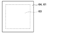
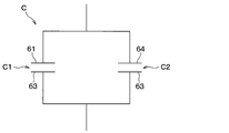
- a lower electrode portion 61 and a ground wiring portion 62 are formed on the first interlayer insulating film 51.
- the lower layer electrode portion 61 has a planar rectangular shape.
- two ground wiring portions 62 are arranged with the lower layer electrode portion 61 interposed therebetween.
- Each ground wiring portion 62 is connected to the well region 14a through the connection via 51d.
- each ground wiring portion 62 is disposed along one opposing side of the lower layer electrode portion 61. That is, in FIG. 1, each ground wiring part 62 is extended along the depth direction of the paper.
- a second interlayer insulating film 52 is formed on the first interlayer insulating film 51 so as to cover the lower layer electrode portion 61 and the ground wiring portion 62.
- the second interlayer insulating film 52 is configured by laminating a second lower insulating film 52a and a second upper insulating film 52b in this order from the SOI substrate 10 side.
- the second lower insulating film 52a is made of an HDP film
- the second upper insulating film 52b is made of a TEOS film or the like.
- the second lower-layer insulating film 52a is composed of the HDP film, so that the second interlayer insulating film 52 is composed of only the TEOS film. The formation of a gap between the lower electrode portion 61 and the ground wiring portion 62 can be suppressed.
- An intermediate electrode portion 63 is formed on the second interlayer insulating film 52 so as to face the lower electrode portion 61.
- the lower electrode portion 61, the intermediate electrode portion 63, the second interlayer insulating film 52 positioned between the lower electrode portion 61 and the intermediate electrode portion 63 is provided, and the second interlayer insulating film 52 serves as a capacitor layer.
- One capacitor C1 is formed.
- the intermediate electrode portion 63 has a planar rectangular shape.
- a third interlayer insulating film 53 is formed on the second interlayer insulating film 52 so as to cover the intermediate electrode portion 63.
- the third interlayer insulating film 53 is configured by sequentially stacking a third lower layer insulating film 53a and a third upper layer insulating film 53b from the SOI substrate 10 side.
- the third lower insulating film 53a is composed of an HDP film
- the third upper insulating film 53b is composed of a TEOS film.
- An upper electrode portion 64 is formed on the third interlayer insulating film 53 so as to face the intermediate electrode portion 63.
- the intermediate electrode portion 63, the upper layer electrode portion 64, the third interlayer insulating film 53 positioned between the intermediate electrode portion 63 and the upper layer electrode portion 64, and the third interlayer insulating film 53 as a capacitance layer are provided.
- a two-capacitor C2 is configured.
- the upper layer electrode portion 64 has a planar rectangular shape.
- a fourth interlayer insulating film 54 is formed on the third interlayer insulating film 53 so as to cover the upper electrode portion 64.
- the fourth interlayer insulating film 54 is made of polyimide resin.
- the lower electrode portion 61, the intermediate electrode portion 63, and the upper layer electrode portion 64 are formed such that the intermediate electrode portion 63 has a smaller planar shape than the lower layer electrode portion 61 and the upper layer electrode portion 64.
- the lower electrode part 61 and the upper electrode part 64 have the same plane size.
- the intermediate electrode part 63 is formed so as to be positioned inside the lower layer electrode part 61 and the upper layer electrode part 64.
- the lower electrode part 61, the intermediate electrode part 63, and the upper electrode part 64 are formed so that the intermediate electrode part 63 does not protrude from the lower electrode part 61 and the upper electrode part 64 when viewed from the normal direction. . Note that viewing from the normal direction to the main surface 10a can also be said to be in the normal direction to the main surface 10a.
- the interval L1 between the lower electrode portion 61 and the intermediate electrode portion 63 in the first capacitor C1 is narrower than the interval L2 between the intermediate electrode portion 63 and the upper electrode portion 64 in the second capacitor C2.
- the thickness of the second interlayer insulating film 52 located between the lower electrode part 61 and the intermediate electrode part 63 is the same as that of the third interlayer insulating film 53 located between the intermediate electrode part 63 and the upper layer electrode part 64. It is thinner than the thickness.
- the lower layer electrode portion 61, the intermediate electrode portion 63, and the upper layer electrode portion 64 are connected to other wiring portions in a cross section different from that in FIG.
- the intermediate electrode portion 63 is set to a high potential
- the lower layer electrode portion 61 and the upper layer electrode portion 64 are set to a low potential.
- the lower layer electrode portion 61 and the upper layer electrode portion 64 are electrically connected via another wiring portion and have the same potential. That is, the capacitor C in the semiconductor device of the present embodiment includes the first capacitor C1 and the second capacitor C2, as shown in FIG. 3, and the first capacitor C1 and the second capacitor C2 are connected in parallel. It is composed of that.
- the wiring portion connected to the lower layer electrode portion 61 and the upper layer electrode portion 64 and the wiring portion connected to the intermediate electrode portion 63 have the respective electrode portions 61, when viewed from the normal direction. It is formed so as to be on the opposite side across 63 and 64. Further, the wiring part connected to the lower electrode part 61 and the upper electrode part 64 and the wiring part connected to the intermediate electrode part 63 are formed so as not to intersect the ground wiring part 62 when viewed from the normal direction.
- the wiring part connected to the lower electrode part 61 and the upper electrode part 64 is drawn to the front side of the paper, and the wiring part connected to the intermediate electrode part 63 is drawn to the depth side of the paper. It is. Thereby, the parasitic capacitance that can be generated between these wiring portions can be reduced.
- ground wiring portion 62 is connected to another wiring portion in a cross section different from that shown in FIG. 1, and is maintained at the ground potential. For this reason, the well region 14a is maintained at the ground potential.
- the lower layer electrode portion 61, the intermediate electrode portion 63, and the upper layer electrode portion 64 are stacked, and the lower layer electrode portion 61 is set to a low potential. For this reason, the parasitic capacitance generated between the SOI substrate 10 and the capacitor C can be reduced.
- the capacitor C has a configuration in which a first capacitor C1 having a lower layer electrode portion 61 and an intermediate electrode portion 63 and a second capacitor C2 having an intermediate electrode portion 63 and an upper layer electrode portion 64 are connected in parallel. For this reason, the capacity per unit area of the capacitor C can be increased.
- the intermediate electrode portion 63 is positioned in the lower layer electrode portion 61 and the upper layer electrode portion 64 when viewed from the normal direction. For this reason, when a positional shift etc. generate
- the intermediate electrode portion 63 is positioned in the lower layer electrode portion 61 when viewed from the normal direction, there is a parasitic capacitance between the intermediate electrode portion 63 that is set to a high potential and the SOI substrate 10. Occurrence can be suppressed.
- the interval L1 of the first capacitor C1 is narrower than the interval L2 of the second capacitor C2.
- the withstand voltage of the capacitor C depends on the first capacitor C1.
- the interlayer insulating films 51 to 54, the electrode portions 61, 63, 64, the ground wiring portion 62, and the like are sequentially formed on the main surface 10a of the SOI substrate 10 from the main surface 10a side.
- the manufacturing error tends to increase as the part is manufactured in a later process.
- the withstand voltage of the capacitor C is prescribed
- region 14a is formed. For this reason, when noise is propagated to the element region 14, the noise can be emitted through the ground wiring portion 62. Therefore, fluctuations in the characteristics of the capacitor C due to noise can also be suppressed.
- the third interlayer insulating film 53 is formed between the third lower insulating film 53a and the third upper insulating film 53b in the third middle from the third lower insulating film 53a side.
- a lower insulating film 53c and a third middle upper insulating film 53d are arranged in this order.
- the third middle lower insulating film 53c is composed of a TEOS film.
- the third middle upper insulating film 53d is made of a nitride film. That is, the second capacitor C2 is configured such that the capacitor layer has an oxide film and a nitride film.
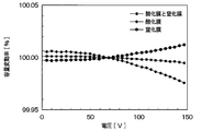
- the capacity fluctuation rate in FIG. 5 indicates the capacity fluctuation rate of each voltage with respect to the reference value, with the capacity at 70 V as the reference value.
- the capacitor layer is formed of an oxide film, it is confirmed that in a region where the voltage is less than 70 V, the capacitance increases with respect to the reference value as the voltage decreases. Further, in the region where the voltage is higher than 70V, it is confirmed that the capacity decreases with respect to the reference value as the voltage increases.
- the capacitor layer is made of a nitride film, it is confirmed that in the region where the voltage is less than 70 V, the capacitance becomes smaller with respect to the reference value as the voltage becomes smaller. In the region where the voltage is higher than 70 V, it is confirmed that the capacity increases with respect to the reference value as the voltage increases.
- the capacitance characteristics with respect to the voltage are opposite between the case where the capacitor layer is formed of an oxide film and the case where the capacitor layer is formed of a nitride film.
- the capacitor layer is composed of an oxide film and a nitride film, the capacitance characteristics of the oxide film and the nitride film are relaxed, so that it is confirmed that the variation in capacitance is reduced.
- the third interlayer insulating film 53 is configured to include the oxide film and the nitride film, so that the variation in capacitance with respect to voltage is reduced.
- the third interlayer insulating film 53 is composed of an oxide film and a nitride film. For this reason, the effect similar to the said 1st Embodiment can be acquired, making the fluctuation
- the third interlayer insulating film 53 includes a nitride film
- the nitride film has a lower moisture permeability than the oxide film. Therefore, the moisture is transmitted to the SOI substrate 10 side from the third middle upper insulating film 53d. Can be suppressed.
- the interval between the first capacitors C1 may be wider than the interval between the second capacitors C2.
- the intermediate electrode part 63 may have a shape protruding from the lower layer electrode part 61 and the upper layer electrode part 64 when viewed from the normal direction.
- the ground wiring portion 62 may not be disposed along the opposing side of the lower layer electrode portion 61 or may not be provided. Even in such a semiconductor device, the parasitic capacitance composed of the SOI substrate 10 and the capacitor C can be reduced by setting the lower electrode portion 61 to a low potential.
- the first to third interlayer insulating films 51 to 53 may be composed only of the HDP film or may be composed only of the TEOS film. That is, the first to third interlayer insulating films 51 to 53 may be composed of only one insulating film. Further, each of the first to third interlayer insulating films 51 to 53 may be further laminated with a plurality of insulating films.
- the second interlayer insulating film 52 may be configured by stacking a TEOS film, an HDP film, and a TEOS film, or may be configured by stacking a plurality of insulating films.
- the number of insulating films constituting the first to third interlayer insulating films 51 to 53 can be appropriately changed.
- the lower layer electrode portion 61, the intermediate electrode portion 63, and the upper layer electrode portion 64 do not have to be a planar rectangular shape, and may be, for example, a circular shape.
- the second interlayer insulating film 52 may have a nitride film. That is, the capacitance layer of the first capacitor C1 may be configured by an oxide film and a nitride film. According to this, the variation of the capacity with respect to the voltage of the first capacitor C1 can be reduced.
- both the capacitor layers of the first capacitor C1 and the second capacitor C2 may be formed of an oxide film and a nitride film, or only the capacitor layer of the first capacitor C1 is formed of an oxide film and a nitride film. You may make it do.
- the third middle-layer insulating film 53c may be disposed on the third lower-layer insulating film 53a without the third middle-layer insulating film 53c.
- the third upper layer insulating film 53b may not be disposed, and the upper layer electrode portion 64 may be disposed on the third middle upper layer insulating film 53d.
Landscapes
- Engineering & Computer Science (AREA)
- Power Engineering (AREA)
- Physics & Mathematics (AREA)
- Condensed Matter Physics & Semiconductors (AREA)
- General Physics & Mathematics (AREA)
- Computer Hardware Design (AREA)
- Microelectronics & Electronic Packaging (AREA)
- Semiconductor Integrated Circuits (AREA)
- Internal Circuitry In Semiconductor Integrated Circuit Devices (AREA)
Priority Applications (1)
| Application Number | Priority Date | Filing Date | Title |
|---|---|---|---|
| US17/084,854 US11476187B2 (en) | 2018-05-21 | 2020-10-30 | Semiconductor device having capacitor on substrate |
Applications Claiming Priority (2)
| Application Number | Priority Date | Filing Date | Title |
|---|---|---|---|
| JP2018097252A JP6988688B2 (ja) | 2018-05-21 | 2018-05-21 | 半導体装置 |
| JP2018-097252 | 2018-05-21 |
Related Child Applications (1)
| Application Number | Title | Priority Date | Filing Date |
|---|---|---|---|
| US17/084,854 Continuation US11476187B2 (en) | 2018-05-21 | 2020-10-30 | Semiconductor device having capacitor on substrate |
Publications (1)
| Publication Number | Publication Date |
|---|---|
| WO2019225339A1 true WO2019225339A1 (ja) | 2019-11-28 |
Family
ID=68615994
Family Applications (1)
| Application Number | Title | Priority Date | Filing Date |
|---|---|---|---|
| PCT/JP2019/018571 Ceased WO2019225339A1 (ja) | 2018-05-21 | 2019-05-09 | 半導体装置 |
Country Status (3)
| Country | Link |
|---|---|
| US (1) | US11476187B2 (enExample) |
| JP (1) | JP6988688B2 (enExample) |
| WO (1) | WO2019225339A1 (enExample) |
Families Citing this family (3)
| Publication number | Priority date | Publication date | Assignee | Title |
|---|---|---|---|---|
| US11901282B2 (en) * | 2019-04-20 | 2024-02-13 | Texas Instruments Incorporated | Device isolators |
| JP7022731B2 (ja) | 2019-11-12 | 2022-02-18 | Kddi株式会社 | 多数のアンテナを選択的に使用する制御装置、制御方法、及びプログラム。 |
| JP7725944B2 (ja) * | 2021-08-30 | 2025-08-20 | 株式会社デンソー | 信号伝送デバイス |
Citations (4)
| Publication number | Priority date | Publication date | Assignee | Title |
|---|---|---|---|---|
| JPH07312415A (ja) * | 1994-05-16 | 1995-11-28 | Yamaha Corp | 半導体集積回路 |
| US20070152295A1 (en) * | 2005-12-29 | 2007-07-05 | Der-Chyang Yeh | Metal-insulator-metal capacitor structure having low voltage dependence |
| JP2009152621A (ja) * | 1996-06-27 | 2009-07-09 | Gennum Corp | 多層膜キャパシタ構造及び方法 |
| JP2016527700A (ja) * | 2013-06-13 | 2016-09-08 | クゥアルコム・インコーポレイテッドQualcomm Incorporated | 金属絶縁体金属キャパシタ構造 |
Family Cites Families (8)
| Publication number | Priority date | Publication date | Assignee | Title |
|---|---|---|---|---|
| JP3603240B2 (ja) | 1997-01-09 | 2004-12-22 | 富士通株式会社 | キャパシタ装置及びその製造方法 |
| JP2001177057A (ja) | 1999-12-17 | 2001-06-29 | Tokyo Electron Ltd | アナログ回路用キャパシタ及びその製造方法 |
| JP4191959B2 (ja) | 2002-06-21 | 2008-12-03 | 富士通株式会社 | 薄膜積層デバイス、回路および薄膜積層デバイスの製造方法 |
| KR100665848B1 (ko) * | 2005-03-21 | 2007-01-09 | 삼성전자주식회사 | 적층 타입 디커플링 커패시터를 갖는 반도체 장치 |
| JP2014229711A (ja) | 2013-05-21 | 2014-12-08 | ルネサスエレクトロニクス株式会社 | 半導体装置 |
| JP2017017272A (ja) | 2015-07-06 | 2017-01-19 | 富士通株式会社 | キャパシタ、半導体装置、キャパシタの製造方法及び半導体装置の製造方法 |
| US10748986B2 (en) * | 2017-11-21 | 2020-08-18 | Taiwan Semiconductor Manufacturing Co., Ltd. | Structure and formation method of semiconductor device with capacitors |
| US11222841B2 (en) * | 2019-09-05 | 2022-01-11 | Texas Instruments Incorporated | Stacked capacitor |
-
2018
- 2018-05-21 JP JP2018097252A patent/JP6988688B2/ja active Active
-
2019
- 2019-05-09 WO PCT/JP2019/018571 patent/WO2019225339A1/ja not_active Ceased
-
2020
- 2020-10-30 US US17/084,854 patent/US11476187B2/en active Active
Patent Citations (4)
| Publication number | Priority date | Publication date | Assignee | Title |
|---|---|---|---|---|
| JPH07312415A (ja) * | 1994-05-16 | 1995-11-28 | Yamaha Corp | 半導体集積回路 |
| JP2009152621A (ja) * | 1996-06-27 | 2009-07-09 | Gennum Corp | 多層膜キャパシタ構造及び方法 |
| US20070152295A1 (en) * | 2005-12-29 | 2007-07-05 | Der-Chyang Yeh | Metal-insulator-metal capacitor structure having low voltage dependence |
| JP2016527700A (ja) * | 2013-06-13 | 2016-09-08 | クゥアルコム・インコーポレイテッドQualcomm Incorporated | 金属絶縁体金属キャパシタ構造 |
Also Published As
| Publication number | Publication date |
|---|---|
| JP6988688B2 (ja) | 2022-01-05 |
| JP2019204826A (ja) | 2019-11-28 |
| US11476187B2 (en) | 2022-10-18 |
| US20210074631A1 (en) | 2021-03-11 |
Similar Documents
| Publication | Publication Date | Title |
|---|---|---|
| CN100407418C (zh) | 半导体器件 | |
| JP2016149409A (ja) | 半導体装置 | |
| WO2019225339A1 (ja) | 半導体装置 | |
| JP2008166731A (ja) | キャパシタ及びこれを用いたキャパシタ内蔵型多層配線基板 | |
| JP2009231513A (ja) | 半導体装置 | |
| KR20190069669A (ko) | 보이드를 포함하는 깊은 트렌치 커패시터 및 이의 제조 방법 | |
| JP6724768B2 (ja) | 半導体装置およびその製造方法 | |
| CN114758989A (zh) | 电容阵列结构及其制备方法、半导体结构 | |
| TWI720555B (zh) | 半導體裝置 | |
| US20170271257A1 (en) | Metallization stack and semiconductor device and electronic device including the same | |
| US10014214B2 (en) | Electronic device including moat power metallization in trench | |
| JP2005057003A (ja) | 半導体集積回路装置 | |
| JP5515245B2 (ja) | 半導体装置及びその製造方法 | |
| CN109585426B (zh) | 高电压电容器、包括电容器的系统以及制造电容器的方法 | |
| CN110896079B (zh) | 半导体存储装置 | |
| JP2005005647A (ja) | 半導体装置およびその製造方法 | |
| JP7087336B2 (ja) | 半導体装置 | |
| KR102857493B1 (ko) | 반도체 장치 | |
| US12034038B2 (en) | Method for manufacturing capacitor structure | |
| JP2021136284A (ja) | 半導体装置及びその製造方法 | |
| US7056841B2 (en) | Method for fabricating semiconductor device | |
| JP2005243828A (ja) | 半導体装置 | |
| JP2024052028A (ja) | 半導体装置およびその製造方法 | |
| JP2012256629A (ja) | 半導体装置及びその製造方法 | |
| JP2008108799A (ja) | 半導体装置 |
Legal Events
| Date | Code | Title | Description |
|---|---|---|---|
| 121 | Ep: the epo has been informed by wipo that ep was designated in this application |
Ref document number: 19807159 Country of ref document: EP Kind code of ref document: A1 |
|
| NENP | Non-entry into the national phase |
Ref country code: DE |
|
| 122 | Ep: pct application non-entry in european phase |
Ref document number: 19807159 Country of ref document: EP Kind code of ref document: A1 |