WO2019203159A1 - Composition conductrice pour un film moulé, film moulé, article moulé et son procédé de production - Google Patents
Composition conductrice pour un film moulé, film moulé, article moulé et son procédé de production Download PDFInfo
- Publication number
- WO2019203159A1 WO2019203159A1 PCT/JP2019/016000 JP2019016000W WO2019203159A1 WO 2019203159 A1 WO2019203159 A1 WO 2019203159A1 JP 2019016000 W JP2019016000 W JP 2019016000W WO 2019203159 A1 WO2019203159 A1 WO 2019203159A1
- Authority
- WO
- WIPO (PCT)
- Prior art keywords
- film
- molded
- conductive
- molded film
- resin
- Prior art date
Links
Images


Classifications
-
- B—PERFORMING OPERATIONS; TRANSPORTING
- B32—LAYERED PRODUCTS
- B32B—LAYERED PRODUCTS, i.e. PRODUCTS BUILT-UP OF STRATA OF FLAT OR NON-FLAT, e.g. CELLULAR OR HONEYCOMB, FORM
- B32B7/00—Layered products characterised by the relation between layers; Layered products characterised by the relative orientation of features between layers, or by the relative values of a measurable parameter between layers, i.e. products comprising layers having different physical, chemical or physicochemical properties; Layered products characterised by the interconnection of layers
- B32B7/02—Physical, chemical or physicochemical properties
- B32B7/025—Electric or magnetic properties
-
- C—CHEMISTRY; METALLURGY
- C08—ORGANIC MACROMOLECULAR COMPOUNDS; THEIR PREPARATION OR CHEMICAL WORKING-UP; COMPOSITIONS BASED THEREON
- C08G—MACROMOLECULAR COMPOUNDS OBTAINED OTHERWISE THAN BY REACTIONS ONLY INVOLVING UNSATURATED CARBON-TO-CARBON BONDS
- C08G18/00—Polymeric products of isocyanates or isothiocyanates
- C08G18/06—Polymeric products of isocyanates or isothiocyanates with compounds having active hydrogen
- C08G18/08—Processes
- C08G18/0804—Manufacture of polymers containing ionic or ionogenic groups
- C08G18/0819—Manufacture of polymers containing ionic or ionogenic groups containing anionic or anionogenic groups
- C08G18/0823—Manufacture of polymers containing ionic or ionogenic groups containing anionic or anionogenic groups containing carboxylate salt groups or groups forming them
-
- B—PERFORMING OPERATIONS; TRANSPORTING
- B29—WORKING OF PLASTICS; WORKING OF SUBSTANCES IN A PLASTIC STATE IN GENERAL
- B29C—SHAPING OR JOINING OF PLASTICS; SHAPING OF MATERIAL IN A PLASTIC STATE, NOT OTHERWISE PROVIDED FOR; AFTER-TREATMENT OF THE SHAPED PRODUCTS, e.g. REPAIRING
- B29C45/00—Injection moulding, i.e. forcing the required volume of moulding material through a nozzle into a closed mould; Apparatus therefor
- B29C45/16—Making multilayered or multicoloured articles
- B29C45/1679—Making multilayered or multicoloured articles applying surface layers onto injection-moulded substrates inside the mould cavity, e.g. in-mould coating [IMC]
-
- B—PERFORMING OPERATIONS; TRANSPORTING
- B32—LAYERED PRODUCTS
- B32B—LAYERED PRODUCTS, i.e. PRODUCTS BUILT-UP OF STRATA OF FLAT OR NON-FLAT, e.g. CELLULAR OR HONEYCOMB, FORM
- B32B27/00—Layered products comprising a layer of synthetic resin
- B32B27/06—Layered products comprising a layer of synthetic resin as the main or only constituent of a layer, which is next to another layer of the same or of a different material
- B32B27/08—Layered products comprising a layer of synthetic resin as the main or only constituent of a layer, which is next to another layer of the same or of a different material of synthetic resin
-
- B—PERFORMING OPERATIONS; TRANSPORTING
- B32—LAYERED PRODUCTS
- B32B—LAYERED PRODUCTS, i.e. PRODUCTS BUILT-UP OF STRATA OF FLAT OR NON-FLAT, e.g. CELLULAR OR HONEYCOMB, FORM
- B32B27/00—Layered products comprising a layer of synthetic resin
- B32B27/18—Layered products comprising a layer of synthetic resin characterised by the use of special additives
- B32B27/20—Layered products comprising a layer of synthetic resin characterised by the use of special additives using fillers, pigments, thixotroping agents
-
- B—PERFORMING OPERATIONS; TRANSPORTING
- B32—LAYERED PRODUCTS
- B32B—LAYERED PRODUCTS, i.e. PRODUCTS BUILT-UP OF STRATA OF FLAT OR NON-FLAT, e.g. CELLULAR OR HONEYCOMB, FORM
- B32B27/00—Layered products comprising a layer of synthetic resin
- B32B27/28—Layered products comprising a layer of synthetic resin comprising synthetic resins not wholly covered by any one of the sub-groups B32B27/30 - B32B27/42
- B32B27/281—Layered products comprising a layer of synthetic resin comprising synthetic resins not wholly covered by any one of the sub-groups B32B27/30 - B32B27/42 comprising polyimides
-
- B—PERFORMING OPERATIONS; TRANSPORTING
- B32—LAYERED PRODUCTS
- B32B—LAYERED PRODUCTS, i.e. PRODUCTS BUILT-UP OF STRATA OF FLAT OR NON-FLAT, e.g. CELLULAR OR HONEYCOMB, FORM
- B32B27/00—Layered products comprising a layer of synthetic resin
- B32B27/28—Layered products comprising a layer of synthetic resin comprising synthetic resins not wholly covered by any one of the sub-groups B32B27/30 - B32B27/42
- B32B27/285—Layered products comprising a layer of synthetic resin comprising synthetic resins not wholly covered by any one of the sub-groups B32B27/30 - B32B27/42 comprising polyethers
-
- B—PERFORMING OPERATIONS; TRANSPORTING
- B32—LAYERED PRODUCTS
- B32B—LAYERED PRODUCTS, i.e. PRODUCTS BUILT-UP OF STRATA OF FLAT OR NON-FLAT, e.g. CELLULAR OR HONEYCOMB, FORM
- B32B27/00—Layered products comprising a layer of synthetic resin
- B32B27/30—Layered products comprising a layer of synthetic resin comprising vinyl (co)polymers; comprising acrylic (co)polymers
- B32B27/304—Layered products comprising a layer of synthetic resin comprising vinyl (co)polymers; comprising acrylic (co)polymers comprising vinyl halide (co)polymers, e.g. PVC, PVDC, PVF, PVDF
-
- B—PERFORMING OPERATIONS; TRANSPORTING
- B32—LAYERED PRODUCTS
- B32B—LAYERED PRODUCTS, i.e. PRODUCTS BUILT-UP OF STRATA OF FLAT OR NON-FLAT, e.g. CELLULAR OR HONEYCOMB, FORM
- B32B27/00—Layered products comprising a layer of synthetic resin
- B32B27/30—Layered products comprising a layer of synthetic resin comprising vinyl (co)polymers; comprising acrylic (co)polymers
- B32B27/308—Layered products comprising a layer of synthetic resin comprising vinyl (co)polymers; comprising acrylic (co)polymers comprising acrylic (co)polymers
-
- B—PERFORMING OPERATIONS; TRANSPORTING
- B32—LAYERED PRODUCTS
- B32B—LAYERED PRODUCTS, i.e. PRODUCTS BUILT-UP OF STRATA OF FLAT OR NON-FLAT, e.g. CELLULAR OR HONEYCOMB, FORM
- B32B27/00—Layered products comprising a layer of synthetic resin
- B32B27/32—Layered products comprising a layer of synthetic resin comprising polyolefins
-
- B—PERFORMING OPERATIONS; TRANSPORTING
- B32—LAYERED PRODUCTS
- B32B—LAYERED PRODUCTS, i.e. PRODUCTS BUILT-UP OF STRATA OF FLAT OR NON-FLAT, e.g. CELLULAR OR HONEYCOMB, FORM
- B32B27/00—Layered products comprising a layer of synthetic resin
- B32B27/34—Layered products comprising a layer of synthetic resin comprising polyamides
-
- B—PERFORMING OPERATIONS; TRANSPORTING
- B32—LAYERED PRODUCTS
- B32B—LAYERED PRODUCTS, i.e. PRODUCTS BUILT-UP OF STRATA OF FLAT OR NON-FLAT, e.g. CELLULAR OR HONEYCOMB, FORM
- B32B27/00—Layered products comprising a layer of synthetic resin
- B32B27/36—Layered products comprising a layer of synthetic resin comprising polyesters
- B32B27/365—Layered products comprising a layer of synthetic resin comprising polyesters comprising polycarbonates
-
- B—PERFORMING OPERATIONS; TRANSPORTING
- B32—LAYERED PRODUCTS
- B32B—LAYERED PRODUCTS, i.e. PRODUCTS BUILT-UP OF STRATA OF FLAT OR NON-FLAT, e.g. CELLULAR OR HONEYCOMB, FORM
- B32B27/00—Layered products comprising a layer of synthetic resin
- B32B27/38—Layered products comprising a layer of synthetic resin comprising epoxy resins
-
- B—PERFORMING OPERATIONS; TRANSPORTING
- B32—LAYERED PRODUCTS
- B32B—LAYERED PRODUCTS, i.e. PRODUCTS BUILT-UP OF STRATA OF FLAT OR NON-FLAT, e.g. CELLULAR OR HONEYCOMB, FORM
- B32B27/00—Layered products comprising a layer of synthetic resin
- B32B27/40—Layered products comprising a layer of synthetic resin comprising polyurethanes
-
- C—CHEMISTRY; METALLURGY
- C08—ORGANIC MACROMOLECULAR COMPOUNDS; THEIR PREPARATION OR CHEMICAL WORKING-UP; COMPOSITIONS BASED THEREON
- C08G—MACROMOLECULAR COMPOUNDS OBTAINED OTHERWISE THAN BY REACTIONS ONLY INVOLVING UNSATURATED CARBON-TO-CARBON BONDS
- C08G18/00—Polymeric products of isocyanates or isothiocyanates
- C08G18/06—Polymeric products of isocyanates or isothiocyanates with compounds having active hydrogen
- C08G18/28—Polymeric products of isocyanates or isothiocyanates with compounds having active hydrogen characterised by the compounds used containing active hydrogen
- C08G18/40—High-molecular-weight compounds
- C08G18/42—Polycondensates having carboxylic or carbonic ester groups in the main chain
- C08G18/4205—Polycondensates having carboxylic or carbonic ester groups in the main chain containing cyclic groups
- C08G18/4208—Polycondensates having carboxylic or carbonic ester groups in the main chain containing cyclic groups containing aromatic groups
- C08G18/4211—Polycondensates having carboxylic or carbonic ester groups in the main chain containing cyclic groups containing aromatic groups derived from aromatic dicarboxylic acids and dialcohols
- C08G18/4213—Polycondensates having carboxylic or carbonic ester groups in the main chain containing cyclic groups containing aromatic groups derived from aromatic dicarboxylic acids and dialcohols from terephthalic acid and dialcohols
-
- C—CHEMISTRY; METALLURGY
- C08—ORGANIC MACROMOLECULAR COMPOUNDS; THEIR PREPARATION OR CHEMICAL WORKING-UP; COMPOSITIONS BASED THEREON
- C08G—MACROMOLECULAR COMPOUNDS OBTAINED OTHERWISE THAN BY REACTIONS ONLY INVOLVING UNSATURATED CARBON-TO-CARBON BONDS
- C08G18/00—Polymeric products of isocyanates or isothiocyanates
- C08G18/06—Polymeric products of isocyanates or isothiocyanates with compounds having active hydrogen
- C08G18/28—Polymeric products of isocyanates or isothiocyanates with compounds having active hydrogen characterised by the compounds used containing active hydrogen
- C08G18/65—Low-molecular-weight compounds having active hydrogen with high-molecular-weight compounds having active hydrogen
- C08G18/66—Compounds of groups C08G18/42, C08G18/48, or C08G18/52
- C08G18/6625—Compounds of groups C08G18/42, C08G18/48, or C08G18/52 with compounds of group C08G18/34
-
- C—CHEMISTRY; METALLURGY
- C08—ORGANIC MACROMOLECULAR COMPOUNDS; THEIR PREPARATION OR CHEMICAL WORKING-UP; COMPOSITIONS BASED THEREON
- C08G—MACROMOLECULAR COMPOUNDS OBTAINED OTHERWISE THAN BY REACTIONS ONLY INVOLVING UNSATURATED CARBON-TO-CARBON BONDS
- C08G18/00—Polymeric products of isocyanates or isothiocyanates
- C08G18/06—Polymeric products of isocyanates or isothiocyanates with compounds having active hydrogen
- C08G18/70—Polymeric products of isocyanates or isothiocyanates with compounds having active hydrogen characterised by the isocyanates or isothiocyanates used
- C08G18/72—Polyisocyanates or polyisothiocyanates
- C08G18/74—Polyisocyanates or polyisothiocyanates cyclic
- C08G18/75—Polyisocyanates or polyisothiocyanates cyclic cycloaliphatic
- C08G18/751—Polyisocyanates or polyisothiocyanates cyclic cycloaliphatic containing only one cycloaliphatic ring
- C08G18/752—Polyisocyanates or polyisothiocyanates cyclic cycloaliphatic containing only one cycloaliphatic ring containing at least one isocyanate or isothiocyanate group linked to the cycloaliphatic ring by means of an aliphatic group
- C08G18/753—Polyisocyanates or polyisothiocyanates cyclic cycloaliphatic containing only one cycloaliphatic ring containing at least one isocyanate or isothiocyanate group linked to the cycloaliphatic ring by means of an aliphatic group containing one isocyanate or isothiocyanate group linked to the cycloaliphatic ring by means of an aliphatic group having a primary carbon atom next to the isocyanate or isothiocyanate group
- C08G18/755—Polyisocyanates or polyisothiocyanates cyclic cycloaliphatic containing only one cycloaliphatic ring containing at least one isocyanate or isothiocyanate group linked to the cycloaliphatic ring by means of an aliphatic group containing one isocyanate or isothiocyanate group linked to the cycloaliphatic ring by means of an aliphatic group having a primary carbon atom next to the isocyanate or isothiocyanate group and at least one isocyanate or isothiocyanate group linked to a secondary carbon atom of the cycloaliphatic ring, e.g. isophorone diisocyanate
-
- C—CHEMISTRY; METALLURGY
- C08—ORGANIC MACROMOLECULAR COMPOUNDS; THEIR PREPARATION OR CHEMICAL WORKING-UP; COMPOSITIONS BASED THEREON
- C08G—MACROMOLECULAR COMPOUNDS OBTAINED OTHERWISE THAN BY REACTIONS ONLY INVOLVING UNSATURATED CARBON-TO-CARBON BONDS
- C08G18/00—Polymeric products of isocyanates or isothiocyanates
- C08G18/06—Polymeric products of isocyanates or isothiocyanates with compounds having active hydrogen
- C08G18/70—Polymeric products of isocyanates or isothiocyanates with compounds having active hydrogen characterised by the isocyanates or isothiocyanates used
- C08G18/72—Polyisocyanates or polyisothiocyanates
- C08G18/77—Polyisocyanates or polyisothiocyanates having heteroatoms in addition to the isocyanate or isothiocyanate nitrogen and oxygen or sulfur
- C08G18/78—Nitrogen
- C08G18/79—Nitrogen characterised by the polyisocyanates used, these having groups formed by oligomerisation of isocyanates or isothiocyanates
- C08G18/791—Nitrogen characterised by the polyisocyanates used, these having groups formed by oligomerisation of isocyanates or isothiocyanates containing isocyanurate groups
- C08G18/792—Nitrogen characterised by the polyisocyanates used, these having groups formed by oligomerisation of isocyanates or isothiocyanates containing isocyanurate groups formed by oligomerisation of aliphatic and/or cycloaliphatic isocyanates or isothiocyanates
-
- C—CHEMISTRY; METALLURGY
- C08—ORGANIC MACROMOLECULAR COMPOUNDS; THEIR PREPARATION OR CHEMICAL WORKING-UP; COMPOSITIONS BASED THEREON
- C08G—MACROMOLECULAR COMPOUNDS OBTAINED OTHERWISE THAN BY REACTIONS ONLY INVOLVING UNSATURATED CARBON-TO-CARBON BONDS
- C08G18/00—Polymeric products of isocyanates or isothiocyanates
- C08G18/06—Polymeric products of isocyanates or isothiocyanates with compounds having active hydrogen
- C08G18/70—Polymeric products of isocyanates or isothiocyanates with compounds having active hydrogen characterised by the isocyanates or isothiocyanates used
- C08G18/72—Polyisocyanates or polyisothiocyanates
- C08G18/80—Masked polyisocyanates
- C08G18/8061—Masked polyisocyanates masked with compounds having only one group containing active hydrogen
- C08G18/807—Masked polyisocyanates masked with compounds having only one group containing active hydrogen with nitrogen containing compounds
-
- C—CHEMISTRY; METALLURGY
- C08—ORGANIC MACROMOLECULAR COMPOUNDS; THEIR PREPARATION OR CHEMICAL WORKING-UP; COMPOSITIONS BASED THEREON
- C08J—WORKING-UP; GENERAL PROCESSES OF COMPOUNDING; AFTER-TREATMENT NOT COVERED BY SUBCLASSES C08B, C08C, C08F, C08G or C08H
- C08J5/00—Manufacture of articles or shaped materials containing macromolecular substances
- C08J5/12—Bonding of a preformed macromolecular material to the same or other solid material such as metal, glass, leather, e.g. using adhesives
- C08J5/121—Bonding of a preformed macromolecular material to the same or other solid material such as metal, glass, leather, e.g. using adhesives by heating
-
- C—CHEMISTRY; METALLURGY
- C08—ORGANIC MACROMOLECULAR COMPOUNDS; THEIR PREPARATION OR CHEMICAL WORKING-UP; COMPOSITIONS BASED THEREON
- C08J—WORKING-UP; GENERAL PROCESSES OF COMPOUNDING; AFTER-TREATMENT NOT COVERED BY SUBCLASSES C08B, C08C, C08F, C08G or C08H
- C08J5/00—Manufacture of articles or shaped materials containing macromolecular substances
- C08J5/18—Manufacture of films or sheets
-
- C—CHEMISTRY; METALLURGY
- C08—ORGANIC MACROMOLECULAR COMPOUNDS; THEIR PREPARATION OR CHEMICAL WORKING-UP; COMPOSITIONS BASED THEREON
- C08K—Use of inorganic or non-macromolecular organic substances as compounding ingredients
- C08K3/00—Use of inorganic substances as compounding ingredients
- C08K3/02—Elements
- C08K3/04—Carbon
-
- C—CHEMISTRY; METALLURGY
- C08—ORGANIC MACROMOLECULAR COMPOUNDS; THEIR PREPARATION OR CHEMICAL WORKING-UP; COMPOSITIONS BASED THEREON
- C08K—Use of inorganic or non-macromolecular organic substances as compounding ingredients
- C08K3/00—Use of inorganic substances as compounding ingredients
- C08K3/02—Elements
- C08K3/08—Metals
-
- C—CHEMISTRY; METALLURGY
- C08—ORGANIC MACROMOLECULAR COMPOUNDS; THEIR PREPARATION OR CHEMICAL WORKING-UP; COMPOSITIONS BASED THEREON
- C08K—Use of inorganic or non-macromolecular organic substances as compounding ingredients
- C08K3/00—Use of inorganic substances as compounding ingredients
- C08K3/18—Oxygen-containing compounds, e.g. metal carbonyls
- C08K3/20—Oxides; Hydroxides
- C08K3/22—Oxides; Hydroxides of metals
-
- C—CHEMISTRY; METALLURGY
- C08—ORGANIC MACROMOLECULAR COMPOUNDS; THEIR PREPARATION OR CHEMICAL WORKING-UP; COMPOSITIONS BASED THEREON
- C08K—Use of inorganic or non-macromolecular organic substances as compounding ingredients
- C08K9/00—Use of pretreated ingredients
- C08K9/02—Ingredients treated with inorganic substances
-
- C—CHEMISTRY; METALLURGY
- C09—DYES; PAINTS; POLISHES; NATURAL RESINS; ADHESIVES; COMPOSITIONS NOT OTHERWISE PROVIDED FOR; APPLICATIONS OF MATERIALS NOT OTHERWISE PROVIDED FOR
- C09D—COATING COMPOSITIONS, e.g. PAINTS, VARNISHES OR LACQUERS; FILLING PASTES; CHEMICAL PAINT OR INK REMOVERS; INKS; CORRECTING FLUIDS; WOODSTAINS; PASTES OR SOLIDS FOR COLOURING OR PRINTING; USE OF MATERIALS THEREFOR
- C09D11/00—Inks
- C09D11/02—Printing inks
- C09D11/03—Printing inks characterised by features other than the chemical nature of the binder
- C09D11/033—Printing inks characterised by features other than the chemical nature of the binder characterised by the solvent
-
- C—CHEMISTRY; METALLURGY
- C09—DYES; PAINTS; POLISHES; NATURAL RESINS; ADHESIVES; COMPOSITIONS NOT OTHERWISE PROVIDED FOR; APPLICATIONS OF MATERIALS NOT OTHERWISE PROVIDED FOR
- C09D—COATING COMPOSITIONS, e.g. PAINTS, VARNISHES OR LACQUERS; FILLING PASTES; CHEMICAL PAINT OR INK REMOVERS; INKS; CORRECTING FLUIDS; WOODSTAINS; PASTES OR SOLIDS FOR COLOURING OR PRINTING; USE OF MATERIALS THEREFOR
- C09D11/00—Inks
- C09D11/02—Printing inks
- C09D11/03—Printing inks characterised by features other than the chemical nature of the binder
- C09D11/037—Printing inks characterised by features other than the chemical nature of the binder characterised by the pigment
-
- C—CHEMISTRY; METALLURGY
- C09—DYES; PAINTS; POLISHES; NATURAL RESINS; ADHESIVES; COMPOSITIONS NOT OTHERWISE PROVIDED FOR; APPLICATIONS OF MATERIALS NOT OTHERWISE PROVIDED FOR
- C09D—COATING COMPOSITIONS, e.g. PAINTS, VARNISHES OR LACQUERS; FILLING PASTES; CHEMICAL PAINT OR INK REMOVERS; INKS; CORRECTING FLUIDS; WOODSTAINS; PASTES OR SOLIDS FOR COLOURING OR PRINTING; USE OF MATERIALS THEREFOR
- C09D11/00—Inks
- C09D11/02—Printing inks
- C09D11/10—Printing inks based on artificial resins
- C09D11/102—Printing inks based on artificial resins containing macromolecular compounds obtained by reactions other than those only involving unsaturated carbon-to-carbon bonds
- C09D11/104—Polyesters
-
- C—CHEMISTRY; METALLURGY
- C09—DYES; PAINTS; POLISHES; NATURAL RESINS; ADHESIVES; COMPOSITIONS NOT OTHERWISE PROVIDED FOR; APPLICATIONS OF MATERIALS NOT OTHERWISE PROVIDED FOR
- C09D—COATING COMPOSITIONS, e.g. PAINTS, VARNISHES OR LACQUERS; FILLING PASTES; CHEMICAL PAINT OR INK REMOVERS; INKS; CORRECTING FLUIDS; WOODSTAINS; PASTES OR SOLIDS FOR COLOURING OR PRINTING; USE OF MATERIALS THEREFOR
- C09D11/00—Inks
- C09D11/02—Printing inks
- C09D11/10—Printing inks based on artificial resins
- C09D11/106—Printing inks based on artificial resins containing macromolecular compounds obtained by reactions only involving carbon-to-carbon unsaturated bonds
- C09D11/107—Printing inks based on artificial resins containing macromolecular compounds obtained by reactions only involving carbon-to-carbon unsaturated bonds from unsaturated acids or derivatives thereof
-
- C—CHEMISTRY; METALLURGY
- C09—DYES; PAINTS; POLISHES; NATURAL RESINS; ADHESIVES; COMPOSITIONS NOT OTHERWISE PROVIDED FOR; APPLICATIONS OF MATERIALS NOT OTHERWISE PROVIDED FOR
- C09D—COATING COMPOSITIONS, e.g. PAINTS, VARNISHES OR LACQUERS; FILLING PASTES; CHEMICAL PAINT OR INK REMOVERS; INKS; CORRECTING FLUIDS; WOODSTAINS; PASTES OR SOLIDS FOR COLOURING OR PRINTING; USE OF MATERIALS THEREFOR
- C09D11/00—Inks
- C09D11/52—Electrically conductive inks
-
- C—CHEMISTRY; METALLURGY
- C09—DYES; PAINTS; POLISHES; NATURAL RESINS; ADHESIVES; COMPOSITIONS NOT OTHERWISE PROVIDED FOR; APPLICATIONS OF MATERIALS NOT OTHERWISE PROVIDED FOR
- C09D—COATING COMPOSITIONS, e.g. PAINTS, VARNISHES OR LACQUERS; FILLING PASTES; CHEMICAL PAINT OR INK REMOVERS; INKS; CORRECTING FLUIDS; WOODSTAINS; PASTES OR SOLIDS FOR COLOURING OR PRINTING; USE OF MATERIALS THEREFOR
- C09D175/00—Coating compositions based on polyureas or polyurethanes; Coating compositions based on derivatives of such polymers
- C09D175/04—Polyurethanes
- C09D175/06—Polyurethanes from polyesters
-
- H—ELECTRICITY
- H01—ELECTRIC ELEMENTS
- H01B—CABLES; CONDUCTORS; INSULATORS; SELECTION OF MATERIALS FOR THEIR CONDUCTIVE, INSULATING OR DIELECTRIC PROPERTIES
- H01B1/00—Conductors or conductive bodies characterised by the conductive materials; Selection of materials as conductors
- H01B1/20—Conductive material dispersed in non-conductive organic material
- H01B1/22—Conductive material dispersed in non-conductive organic material the conductive material comprising metals or alloys
-
- H—ELECTRICITY
- H01—ELECTRIC ELEMENTS
- H01B—CABLES; CONDUCTORS; INSULATORS; SELECTION OF MATERIALS FOR THEIR CONDUCTIVE, INSULATING OR DIELECTRIC PROPERTIES
- H01B5/00—Non-insulated conductors or conductive bodies characterised by their form
- H01B5/14—Non-insulated conductors or conductive bodies characterised by their form comprising conductive layers or films on insulating-supports
-
- H—ELECTRICITY
- H05—ELECTRIC TECHNIQUES NOT OTHERWISE PROVIDED FOR
- H05K—PRINTED CIRCUITS; CASINGS OR CONSTRUCTIONAL DETAILS OF ELECTRIC APPARATUS; MANUFACTURE OF ASSEMBLAGES OF ELECTRICAL COMPONENTS
- H05K3/00—Apparatus or processes for manufacturing printed circuits
- H05K3/10—Apparatus or processes for manufacturing printed circuits in which conductive material is applied to the insulating support in such a manner as to form the desired conductive pattern
- H05K3/103—Apparatus or processes for manufacturing printed circuits in which conductive material is applied to the insulating support in such a manner as to form the desired conductive pattern by bonding or embedding conductive wires or strips
-
- B—PERFORMING OPERATIONS; TRANSPORTING
- B29—WORKING OF PLASTICS; WORKING OF SUBSTANCES IN A PLASTIC STATE IN GENERAL
- B29K—INDEXING SCHEME ASSOCIATED WITH SUBCLASSES B29B, B29C OR B29D, RELATING TO MOULDING MATERIALS OR TO MATERIALS FOR MOULDS, REINFORCEMENTS, FILLERS OR PREFORMED PARTS, e.g. INSERTS
- B29K2669/00—Use of PC, i.e. polycarbonates or derivatives thereof for preformed parts, e.g. for inserts
-
- B—PERFORMING OPERATIONS; TRANSPORTING
- B32—LAYERED PRODUCTS
- B32B—LAYERED PRODUCTS, i.e. PRODUCTS BUILT-UP OF STRATA OF FLAT OR NON-FLAT, e.g. CELLULAR OR HONEYCOMB, FORM
- B32B2250/00—Layers arrangement
- B32B2250/02—2 layers
-
- B—PERFORMING OPERATIONS; TRANSPORTING
- B32—LAYERED PRODUCTS
- B32B—LAYERED PRODUCTS, i.e. PRODUCTS BUILT-UP OF STRATA OF FLAT OR NON-FLAT, e.g. CELLULAR OR HONEYCOMB, FORM
- B32B2250/00—Layers arrangement
- B32B2250/24—All layers being polymeric
-
- B—PERFORMING OPERATIONS; TRANSPORTING
- B32—LAYERED PRODUCTS
- B32B—LAYERED PRODUCTS, i.e. PRODUCTS BUILT-UP OF STRATA OF FLAT OR NON-FLAT, e.g. CELLULAR OR HONEYCOMB, FORM
- B32B2255/00—Coating on the layer surface
- B32B2255/10—Coating on the layer surface on synthetic resin layer or on natural or synthetic rubber layer
-
- B—PERFORMING OPERATIONS; TRANSPORTING
- B32—LAYERED PRODUCTS
- B32B—LAYERED PRODUCTS, i.e. PRODUCTS BUILT-UP OF STRATA OF FLAT OR NON-FLAT, e.g. CELLULAR OR HONEYCOMB, FORM
- B32B2255/00—Coating on the layer surface
- B32B2255/26—Polymeric coating
-
- B—PERFORMING OPERATIONS; TRANSPORTING
- B32—LAYERED PRODUCTS
- B32B—LAYERED PRODUCTS, i.e. PRODUCTS BUILT-UP OF STRATA OF FLAT OR NON-FLAT, e.g. CELLULAR OR HONEYCOMB, FORM
- B32B2264/00—Composition or properties of particles which form a particulate layer or are present as additives
- B32B2264/10—Inorganic particles
- B32B2264/102—Oxide or hydroxide
-
- B—PERFORMING OPERATIONS; TRANSPORTING
- B32—LAYERED PRODUCTS
- B32B—LAYERED PRODUCTS, i.e. PRODUCTS BUILT-UP OF STRATA OF FLAT OR NON-FLAT, e.g. CELLULAR OR HONEYCOMB, FORM
- B32B2264/00—Composition or properties of particles which form a particulate layer or are present as additives
- B32B2264/10—Inorganic particles
- B32B2264/105—Metal
- B32B2264/1051—Silver or gold
-
- B—PERFORMING OPERATIONS; TRANSPORTING
- B32—LAYERED PRODUCTS
- B32B—LAYERED PRODUCTS, i.e. PRODUCTS BUILT-UP OF STRATA OF FLAT OR NON-FLAT, e.g. CELLULAR OR HONEYCOMB, FORM
- B32B2264/00—Composition or properties of particles which form a particulate layer or are present as additives
- B32B2264/10—Inorganic particles
- B32B2264/105—Metal
- B32B2264/1055—Copper or nickel
-
- B—PERFORMING OPERATIONS; TRANSPORTING
- B32—LAYERED PRODUCTS
- B32B—LAYERED PRODUCTS, i.e. PRODUCTS BUILT-UP OF STRATA OF FLAT OR NON-FLAT, e.g. CELLULAR OR HONEYCOMB, FORM
- B32B2264/00—Composition or properties of particles which form a particulate layer or are present as additives
- B32B2264/10—Inorganic particles
- B32B2264/107—Ceramic
- B32B2264/108—Carbon, e.g. graphite particles
-
- B—PERFORMING OPERATIONS; TRANSPORTING
- B32—LAYERED PRODUCTS
- B32B—LAYERED PRODUCTS, i.e. PRODUCTS BUILT-UP OF STRATA OF FLAT OR NON-FLAT, e.g. CELLULAR OR HONEYCOMB, FORM
- B32B2307/00—Properties of the layers or laminate
- B32B2307/20—Properties of the layers or laminate having particular electrical or magnetic properties, e.g. piezoelectric
- B32B2307/202—Conductive
-
- B—PERFORMING OPERATIONS; TRANSPORTING
- B32—LAYERED PRODUCTS
- B32B—LAYERED PRODUCTS, i.e. PRODUCTS BUILT-UP OF STRATA OF FLAT OR NON-FLAT, e.g. CELLULAR OR HONEYCOMB, FORM
- B32B2307/00—Properties of the layers or laminate
- B32B2307/30—Properties of the layers or laminate having particular thermal properties
-
- B—PERFORMING OPERATIONS; TRANSPORTING
- B32—LAYERED PRODUCTS
- B32B—LAYERED PRODUCTS, i.e. PRODUCTS BUILT-UP OF STRATA OF FLAT OR NON-FLAT, e.g. CELLULAR OR HONEYCOMB, FORM
- B32B2307/00—Properties of the layers or laminate
- B32B2307/50—Properties of the layers or laminate having particular mechanical properties
- B32B2307/54—Yield strength; Tensile strength
-
- B—PERFORMING OPERATIONS; TRANSPORTING
- B32—LAYERED PRODUCTS
- B32B—LAYERED PRODUCTS, i.e. PRODUCTS BUILT-UP OF STRATA OF FLAT OR NON-FLAT, e.g. CELLULAR OR HONEYCOMB, FORM
- B32B2457/00—Electrical equipment
-
- B—PERFORMING OPERATIONS; TRANSPORTING
- B32—LAYERED PRODUCTS
- B32B—LAYERED PRODUCTS, i.e. PRODUCTS BUILT-UP OF STRATA OF FLAT OR NON-FLAT, e.g. CELLULAR OR HONEYCOMB, FORM
- B32B2605/00—Vehicles
- B32B2605/08—Cars
-
- C—CHEMISTRY; METALLURGY
- C08—ORGANIC MACROMOLECULAR COMPOUNDS; THEIR PREPARATION OR CHEMICAL WORKING-UP; COMPOSITIONS BASED THEREON
- C08J—WORKING-UP; GENERAL PROCESSES OF COMPOUNDING; AFTER-TREATMENT NOT COVERED BY SUBCLASSES C08B, C08C, C08F, C08G or C08H
- C08J2333/00—Characterised by the use of homopolymers or copolymers of compounds having one or more unsaturated aliphatic radicals, each having only one carbon-to-carbon double bond, and only one being terminated by only one carboxyl radical, or of salts, anhydrides, esters, amides, imides, or nitriles thereof; Derivatives of such polymers
-
- C—CHEMISTRY; METALLURGY
- C08—ORGANIC MACROMOLECULAR COMPOUNDS; THEIR PREPARATION OR CHEMICAL WORKING-UP; COMPOSITIONS BASED THEREON
- C08J—WORKING-UP; GENERAL PROCESSES OF COMPOUNDING; AFTER-TREATMENT NOT COVERED BY SUBCLASSES C08B, C08C, C08F, C08G or C08H
- C08J2363/00—Characterised by the use of epoxy resins; Derivatives of epoxy resins
-
- C—CHEMISTRY; METALLURGY
- C08—ORGANIC MACROMOLECULAR COMPOUNDS; THEIR PREPARATION OR CHEMICAL WORKING-UP; COMPOSITIONS BASED THEREON
- C08J—WORKING-UP; GENERAL PROCESSES OF COMPOUNDING; AFTER-TREATMENT NOT COVERED BY SUBCLASSES C08B, C08C, C08F, C08G or C08H
- C08J2367/00—Characterised by the use of polyesters obtained by reactions forming a carboxylic ester link in the main chain; Derivatives of such polymers
- C08J2367/02—Polyesters derived from dicarboxylic acids and dihydroxy compounds
-
- C—CHEMISTRY; METALLURGY
- C08—ORGANIC MACROMOLECULAR COMPOUNDS; THEIR PREPARATION OR CHEMICAL WORKING-UP; COMPOSITIONS BASED THEREON
- C08J—WORKING-UP; GENERAL PROCESSES OF COMPOUNDING; AFTER-TREATMENT NOT COVERED BY SUBCLASSES C08B, C08C, C08F, C08G or C08H
- C08J2375/00—Characterised by the use of polyureas or polyurethanes; Derivatives of such polymers
- C08J2375/04—Polyurethanes
- C08J2375/06—Polyurethanes from polyesters
-
- C—CHEMISTRY; METALLURGY
- C08—ORGANIC MACROMOLECULAR COMPOUNDS; THEIR PREPARATION OR CHEMICAL WORKING-UP; COMPOSITIONS BASED THEREON
- C08K—Use of inorganic or non-macromolecular organic substances as compounding ingredients
- C08K3/00—Use of inorganic substances as compounding ingredients
- C08K3/02—Elements
- C08K3/08—Metals
- C08K2003/0806—Silver
-
- C—CHEMISTRY; METALLURGY
- C08—ORGANIC MACROMOLECULAR COMPOUNDS; THEIR PREPARATION OR CHEMICAL WORKING-UP; COMPOSITIONS BASED THEREON
- C08K—Use of inorganic or non-macromolecular organic substances as compounding ingredients
- C08K3/00—Use of inorganic substances as compounding ingredients
- C08K3/02—Elements
- C08K3/08—Metals
- C08K2003/085—Copper
-
- C—CHEMISTRY; METALLURGY
- C08—ORGANIC MACROMOLECULAR COMPOUNDS; THEIR PREPARATION OR CHEMICAL WORKING-UP; COMPOSITIONS BASED THEREON
- C08K—Use of inorganic or non-macromolecular organic substances as compounding ingredients
- C08K3/00—Use of inorganic substances as compounding ingredients
- C08K3/18—Oxygen-containing compounds, e.g. metal carbonyls
- C08K3/20—Oxides; Hydroxides
- C08K3/22—Oxides; Hydroxides of metals
- C08K2003/2231—Oxides; Hydroxides of metals of tin
-
- C—CHEMISTRY; METALLURGY
- C08—ORGANIC MACROMOLECULAR COMPOUNDS; THEIR PREPARATION OR CHEMICAL WORKING-UP; COMPOSITIONS BASED THEREON
- C08K—Use of inorganic or non-macromolecular organic substances as compounding ingredients
- C08K2201/00—Specific properties of additives
- C08K2201/001—Conductive additives
-
- H—ELECTRICITY
- H05—ELECTRIC TECHNIQUES NOT OTHERWISE PROVIDED FOR
- H05K—PRINTED CIRCUITS; CASINGS OR CONSTRUCTIONAL DETAILS OF ELECTRIC APPARATUS; MANUFACTURE OF ASSEMBLAGES OF ELECTRICAL COMPONENTS
- H05K1/00—Printed circuits
- H05K1/02—Details
- H05K1/09—Use of materials for the conductive, e.g. metallic pattern
- H05K1/092—Dispersed materials, e.g. conductive pastes or inks
- H05K1/095—Dispersed materials, e.g. conductive pastes or inks for polymer thick films, i.e. having a permanent organic polymeric binder
Definitions
- the present invention relates to a conductive composition for a molded film, a molded film, a molded body, and a method for producing the same.
- Patent Document 1 discloses a resin molded body, a base film embedded so as to be flush with one surface of the resin molded body, and a conductive circuit disposed between the resin molded body and the base film.
- a specific conductive circuit integrated molded product having the following is disclosed.
- a base film on which a specific conductive circuit is formed is placed on a cavity surface of an injection mold, and then a molten resin is injected to form a resin. It is described that the molded body is injection-molded.
- the conductive circuit is formed by etching a specific transparent metal thin film.
- Patent Document 2 discloses a specific conductive material containing specific conductive fine particles and a specific epoxy resin as a low-temperature treatment type conductive ink capable of forming a high-definition conductive pattern by screen printing. Ink has been disclosed. According to screen printing, the conductive pattern can be made thicker and the resistance of the conductive pattern can be reduced.
- diethylene glycol monoethyl ether acetate is used as a solvent for the conductive ink.
- Patent Document 3 as a method for producing a decorative sheet capable of expressing a three-dimensional stereoscopic effect, a laminate having a printed layer printed in a pattern on a transparent resin layer, and a base film A method is disclosed in which the decorative layer is formed into a concavo-convex shape along the pattern of the printed layer by thermocompression bonding with a laminated sheet having a decorative layer thereon.
- a conductor can be easily provided on the surface of a molded body.
- a conductive circuit on the surface of a substrate having various shapes such as a substrate having an uneven surface or a curved surface.
- the film needs to be deformed according to the surface shape of the substrate.
- a large tensile force may be partially generated in the conductive layer. The tensile force caused breakage of the conductive layer, and a decrease in conductivity became a problem.
- This invention is made
- the electroconductive fall for the molding film conductive composition which can manufacture the shaping
- the conductive composition for molded film according to this embodiment is Containing resin (A), conductive fine particles (B), and solvent (C),
- the solvent (C) satisfies the following condition (1) and satisfies at least one of the conditions (2-1) and (2-2).
- Boiling point is 180 ° C. or higher and 270 ° C. or lower
- polarity parameter ⁇ p is 0 ⁇ ⁇ p ⁇ 5.0
- Hansen solubility parameter (HSP) The hydrogen bond parameter ⁇ h of 9.8 ⁇ ⁇ h ⁇ 24.0
- the solvent (C ′) further satisfies the following condition (2-3).
- the dispersion parameter ⁇ d of the Hansen solubility parameter (HSP) is 14.0 ⁇ ⁇ d ⁇ 20.0.
- the conductive fine particles (B) are selected from silver powder, copper powder, silver coat powder, copper alloy powder, conductive oxide powder, and carbon fine particles.
- One or more conductive fine particles are selected from silver powder, copper powder, silver coat powder, copper alloy powder, conductive oxide powder, and carbon fine particles.
- the resin (A) has one or more substituents selected from a hydroxy group, an amino group, a carboxyl group, and an acid anhydride group.
- the resin (A) has at least one reactive functional group selected from a hydroxy group, an amino group, a carboxyl group, and an acid anhydride group.
- a crosslinking agent (D) having two or more reactive functional groups in the molecule and two or more reactive functional groups capable of crosslinking with the reactive functional group of the resin (A) is further contained.
- the resin (A) has a weight average molecular weight of 20,000 or more and 600,000 or less, The ratio of the total amount F D (mol) of the second reactive functional group of the crosslinking agent (D) to the mass M A (g) of the resin (A) satisfies the following formula (1).
- Formula (1) 5.0 ⁇ 10 ⁇ 5 ⁇ F D / M A ⁇ 6.0 ⁇ 10 ⁇ 4
- the molded film according to this embodiment is a molded film having a conductive layer on a base film,
- the conductive layer is a cured product of the conductive composition for molded film of the present embodiment.
- the relationship between the breaking elongation of each layer at the softening point temperature of the base film satisfies the breaking elongation of the base film> the breaking elongation of the conductive layer.
- One embodiment of the molded film of the present embodiment is a molded film having a decorative layer and a conductive layer on a base film,
- the conductive layer is a cured product of the conductive composition for molded film of the present embodiment.
- the relationship between the elongation at break of each layer at the softening point temperature of the base film satisfies the elongation at break of the base film> the elongation at break of the decorative layer> the elongation at break of the conductive layer.
- the base film is a film selected from polycarbonate, polymethyl methacrylate, and polyethylene terephthalate, or a laminated film thereof.
- the molded body according to the present embodiment is a molded body in which a conductive layer is laminated on a base material,
- the conductive layer is a cured product of the conductive composition for molded film.
- the first manufacturing method of the molded body according to the present embodiment includes a step of printing the conductive composition for a molded film of the present embodiment on a base film and manufacturing the molded film by drying, Placing the molded film on a substrate; And a step of integrating the molded film and the base material by an overlay molding method.
- the second production method of the molded body according to the present embodiment includes a step of printing the conductive composition for a molded film of the present embodiment on a base film and producing a molded film by drying, Forming the molded film into a predetermined shape; Placing the molded film after molding in a mold for injection molding; Forming a base material by injection molding, and integrating the molded film and the base material.
- the third manufacturing method of the molded body according to the present embodiment includes a step of printing the conductive composition for a molded film of the present embodiment on a base film and manufacturing the molded film by drying, Placing the molded film in a mold for injection molding; And forming a substrate by injection molding and transferring the conductive layer in the molded film to the substrate side.
- a conductive composition for a molded film capable of producing a molded film in which a decrease in conductivity due to tensile force is suppressed, a molded film in which a decrease in conductivity due to tensile force is suppressed, and conductivity
- An excellent molded body and a method for producing the same can be provided.
- the cured product includes not only a product cured by a chemical reaction but also a product cured without a chemical reaction, such as a product hardened by volatilization of a solvent.
- the conductive composition for molded film of the present embodiment contains a resin (A), conductive fine particles (B), and a solvent (C), The solvent (C) satisfies the following condition (1) and satisfies at least one of the conditions (2-1) and (2-2). Including 40 parts by mass or more.
- Boiling point is 180 ° C. or higher and 270 ° C. or lower
- Hansen solubility parameter (HSP) polarity parameter ⁇ p is 0 ⁇ ⁇ p ⁇ 5.0
- Hansen solubility parameter (HSP ) Has a hydrogen bond parameter ⁇ h of 9.8 ⁇ ⁇ h ⁇ 24.0
- a molded film in which the decrease in conductivity due to tensile force is suppressed can be produced.
- the present inventors have examined a conductive composition that can be screen-printed.
- a solvent having a boiling point of 180 ° C. or higher and 270 ° C. or lower was selected and examined.
- the resistance value generated when the obtained molded film was pulled.
- the present inventors have found that when a conductive composition containing a specific solvent is printed and heat-dried on a resin film, the contact surface between the conductive composition and the resin film.
- the molded film when used as a molded film that follows and integrates the shape of the substrate surface that is not flat, the molded film is deformed. During the deformation, the molded film is subjected to friction with the mold or tensile force. In the case of a molded film having a resin film infiltrated with solvent, dissolved or shrunk, during the deformation, the conductive layer is detached due to the friction or cohesive force reduction, or the conductive layer is disconnected due to stretching. Presumed to be.
- the present inventors have found that the polarity parameter ⁇ p of the Hansen solubility parameter (HSP) exceeds 5.0, and the hydrogen bonding parameter ⁇ h of the Hansen solubility parameter is 9 It was found that a solvent of less than .8 easily penetrates into the base film. That is, the solvent has a Hansen solubility parameter (HSP) polarity parameter ⁇ p of 0 ⁇ ⁇ p ⁇ 5.0 or a Hansen solubility parameter (HSP) hydrogen bond parameter ⁇ h of 9.8 ⁇ ⁇ h ⁇ 24.0.
- HSP Hansen solubility parameter
- the conductive composition for molded film of the present invention can easily produce a molded film having a thick conductive layer excellent in conductivity by screen printing or the like. Can do. Moreover, even if the shaping
- the conductive composition for molded film of this embodiment contains at least the resin (A), the conductive fine particles (B), and the solvent (C), and further contains other components as necessary. It may be contained.
- each component of such a conductive composition for molded films will be described.
- the conductive composition of the present embodiment contains a binder resin (A) in order to impart film formability and adhesion to a base film or a decorative layer. Moreover, in this implementation, a softness
- the resin (A) can be appropriately selected from resins used for conductive composition applications.
- the resin (A) include acrylic resins, vinyl ether resins, polyether resins, polyester resins, polyurethane resins, epoxy resins, phenoxy resins, polycarbonate resins, polyvinyl chloride resins, polyolefin resins, and styrene.
- examples thereof include a system block copolymer resin, a polyamide resin, and a polyimide resin, and these can be used alone or in combination of two or more.
- the resin (A) preferably has a substituent selected from a hydroxy group, an amino group, a carboxyl group, and an acid anhydride group.
- affinity with the electroconductive fine particles (B) mentioned later improves, and the adhesiveness to a base film etc. also improves.
- the resin (A) preferably has two or more substituents selected from a hydroxy group, an amino group, a carboxyl group, and an acid anhydride group in one molecule.
- the resin (A) can be three-dimensionally cross-linked by combining with a cross-linking agent (D) described later, and can be suitably used in applications where the conductive layer requires hardness.
- the functional group value is preferably 1 mgKOH / g or more and 400 mgKOH / g or less, It is preferable that they are 2 mgKOH / g or more and 350 mgKOH / g or less.
- the details of the method for calculating the functional group value will be described in Examples described later.
- resin (A) has multiple types of functional group, let functional group value be the sum total. For example, when the resin (A) has a hydroxy group and a carboxyl group, the functional group value represents the total of the hydroxyl value and acid value of the resin (A).
- the weight average molecular weight of resin (A) is not specifically limited, From the point of the handleability at the time of coating film formation, it is preferable that it is 5,000 or more and 1,000,000 or less, and 10,000 or more and 800,000 or less. Is more preferable, and 20,000 or more and 600,000 or less are more preferable.
- the weight average molecular weight is a molecular weight in terms of polystyrene as measured using GPC (gel permeation chromatography) “HLC-8320” manufactured by Tosoh Corporation.
- the glass transition temperature (Tg) of the resin (A) is not particularly limited, but the glass transition temperature (Tg) of the resin (A) is 0 ° C. or higher and 150 ° C. or lower from the viewpoint of easy handling of the conductive layer. Is preferable, and it is more preferable that it is 5 degreeC or more and 120 degrees C or less.
- the resin (A) may be synthesized by the examples described later and other known methods, or a commercially available product having desired physical properties may be used. In this embodiment, the resin (A) can be used alone or in combination of two or more.
- the content ratio of the resin (A) in the conductive composition of the present embodiment is not particularly limited as long as it is appropriately adjusted depending on the application, etc., but is 5% by mass or more based on the total solid content contained in the conductive composition. It is preferably 50% by mass or less, and more preferably 8% by mass or more and 40% by mass or less.
- the content ratio of the resin (A) is not less than the above lower limit value, film formability and adhesion to a base film can be improved, and flexibility can be imparted to the conductive layer.
- the content rate of resin (A) is below the said upper limit, the content rate of electroconductive fine particles (B) can be raised relatively and the conductive layer excellent in electroconductivity can be formed.
- the conductive fine particles (B) are those in which a plurality of conductive fine particles come into contact with each other in the conductive layer to develop conductivity.
- the conductive fine particles (B) are appropriately selected from those that can be obtained without heating at high temperatures. Select and use. Examples of the conductive fine particles used in this embodiment include metal fine particles, carbon fine particles, and conductive oxide fine particles.
- Examples of the metal fine particles include simple metal powders such as gold, silver, copper, nickel, chromium, palladium, rhodium, ruthenium, indium, aluminum, tungsten, morphbutene, platinum, copper-nickel alloy, silver-palladium alloy, Examples thereof include alloy powders such as copper-tin alloy, silver-copper alloy, copper-manganese alloy, and metal-coated powder in which the surface of the single metal powder or alloy powder is coated with silver or the like.
- Examples of the carbon fine particles include carbon black, graphite, and carbon nanotube.
- Examples of the conductive oxide fine particles include silver oxide, indium oxide, tin oxide, zinc oxide, and ruthenium oxide.
- conductive fine particles selected from silver powder, copper powder, silver coat powder, copper alloy powder, conductive oxide powder, and carbon fine particles.
- the shape of the conductive fine particles (B) is not particularly limited, and an indeterminate shape, an aggregated shape, a scale shape, a microcrystalline shape, a spherical shape, a flake shape, a wire shape, and the like can be appropriately used. From the viewpoint of maintaining conductivity at the time of molding and from the viewpoint of adhesion of the conductor pattern to the substrate, agglomerated, scale-like, flake-like, and wire-like ones are preferred.
- the average particle size of the conductive fine particles is not particularly limited, but is preferably 0.1 ⁇ m or more and 50 ⁇ m or less, more preferably 0.5 ⁇ m or more from the viewpoint of dispersibility in the conductive composition and conductivity when the conductive layer is formed. 30 ⁇ m or less is more preferable.
- the average particle size of the conductive fine particles (B) is calculated as follows.
- a commercially available surfactant polyoxyethylene octylphenyl is used as a dispersant using a laser diffraction / scattering particle size distribution measuring device (manufactured by Nikkiso Co., Ltd .: Microtrack 9220FRA).
- An appropriate amount of conductive fine particles (B) was added to an aqueous solution containing 0.5% by volume of ether (Roche Diagnostics Co., Ltd .: Triton X-100), and 40 W ultrasonic waves were irradiated for 180 seconds while stirring. Later, measurements were taken.
- the calculated median diameter (D50) was taken as the average particle diameter of the conductive fine particles (B).
- the conductive fine particles (B) can be used singly or in combination of two or more.
- the content ratio of the conductive fine particles (B) in the conductive composition of the present embodiment is not particularly limited as long as it is appropriately adjusted according to the use, etc., but is 50 mass with respect to the total solid content contained in the conductive composition. % To 95% by mass, preferably 60% to 90% by mass. If the content rate of electroconductive fine particles (B) is more than the said lower limit, the electroconductive layer excellent in electroconductivity can be formed. Moreover, if the content rate of electroconductive fine particles (B) is below the said upper limit, the content rate of resin (A) can be raised, film-forming property, adhesiveness to a base film, etc. will improve, , Flexibility can be imparted to the conductive layer.
- the solvent (C) satisfies the following condition (1)
- the solvent (C ′) satisfies at least one of the conditions (2-1) and (2-2).
- (1) Boiling point is 180 ° C. or higher and 270 ° C. or lower
- Hansen solubility parameter (HSP) polarity parameter ⁇ p is 0 ⁇ ⁇ p ⁇ 5.0
- Hansen solubility parameter (HSP) The hydrogen bond parameter ⁇ h of 9.8 ⁇ ⁇ h ⁇ 24.0
- the proportion of the solvent (C ′) may be 40% by mass or more and 100% by mass or less, preferably 60% by mass or more, and more preferably 80% by mass or more with respect to the whole solvent.
- the hydrogen bonding parameter ⁇ h of the Hansen solubility parameter (HSP) is preferably 2.9 ⁇ ⁇ h ⁇ 9.1.
- the solvent (C ′) satisfying the condition (2-2) preferably further has a Hansen solubility parameter (HSP) polarity parameter ⁇ p of 5.5 ⁇ ⁇ p ⁇ 15.3.
- the dispersion parameter ⁇ d of the Hansen solubility parameter (HSP) is 14.0 ⁇ ⁇ d ⁇ 20.0.
- the solvent (C) may contain a solvent other than the solvent (C ′) in a range of less than 60% by mass.
- a solvent C-1 that satisfies the condition (1) and does not satisfy the condition (2), and a solvent (C-2) that does not satisfy the condition 1 and has a boiling point of less than 180 ° C. Can be mentioned.
- the solvent (C-1) is a solvent that penetrates into the base film and dissolves or shrinks. Therefore, although the dissolution or shrinkage can be greatly reduced by using in combination with the solvent (C ′), the solvent (C-1) is 40% by mass relative to the total amount of the solvent (C).
- the content is preferably not more than 20% by mass, more preferably not more than 20% by mass, and still more preferably 0% by mass, that is, substantially not contained.
- the solvent corresponding to the solvent (C-1) include diethylene glycol monoethyl ether acetate, gamma butyrolactone, and isophorone.
- the solvent (C-2) having a boiling point of less than 180 ° C. evaporates relatively quickly due to the drying heat after screen printing even if the condition (2) is not satisfied. short. Therefore, although the action of penetrating into the base film and dissolving or shrinking is small, if it is used in a large amount, the volatility at the time of printing is too high, and stable continuous printing becomes extremely difficult. Therefore, with respect to the total amount of the solvent (C) It is preferable that it is 30 mass% or less. Examples of the solvent (C-2) having a boiling point of less than 180 ° C.
- the ratio of the solvent (C) with respect to the whole electroconductive composition of this execution is not specifically limited, From the point of the handleability at the time of screen printing, it is preferable that it is 5 to 60 mass%, and is 10 to 50 mass%. It is more preferable that the amount is not more than mass%.
- the conductive composition of the present invention may further contain other components as necessary.
- other components in addition to the crosslinking agent (D), a dispersant, an antifriction agent, an infrared absorber, an ultraviolet absorber, an aromatic, an antioxidant, an organic pigment, an inorganic pigment, an antifoaming agent, Examples include silane coupling agents, plasticizers, flame retardants, moisturizers, etc.
- the crosslinking agent (D) is used for crosslinking the resin (A).
- a crosslinking agent (D) it can select and use suitably from what has two or more reactive functional groups which can carry out a crosslinking formation with the reactive functional group which the said resin (A) has.
- reactive functional groups include epoxy groups, isocyanate groups, blocked isocyanate groups, alkyloxyamino groups, aziridinyl groups, oxetanyl groups, carbodiimide groups, ⁇ -hydroxyalkylamide groups, and the like.
- the proportion is preferably 0.05 parts by mass or more and 30 parts by mass or less, more preferably 1 part by mass or more and 25 parts by mass or less with respect to 100 parts by mass of the resin (A). preferable.
- the resin (A) has two or more first reactive functional groups selected from a hydroxy group, an amino group, a carboxyl group, and an acid anhydride group in one molecule, and the weight One having an average molecular weight of 20,000 or more and 600,000 or less is selected, and as the crosslinking agent (D), 2 reactive functional groups capable of crosslinking with the first reactive functional group are contained in 2 molecules in 1 molecule. Choose one that has more than one, The ratio of the total amount F D (mol) of the substance amount of the second reactive functional group of the cross-linking agent (D) and the mass M A (g) of the resin (A) satisfies the following formula (1) It is particularly preferable to combine them with each other.
- the method for producing a conductive composition of the present embodiment is a method in which the resin (A), the conductive fine particles (B) and other components used as necessary are dissolved or dispersed in a solvent (C). Well, it can be produced by mixing by known mixing means.
- the molded film of the present embodiment is a molded film having a conductive layer on a base film,
- the conductive layer is a cured product of the conductive composition for molded film.
- the layer structure of the molded film of this embodiment will be described with reference to FIGS.
- FIG.1 and FIG.2 is typical sectional drawing which shows an example of the shaping
- a molded film 10 shown in the example of FIG. 1 includes a conductive layer 2 on a base film 1.
- the conductive layer 2 may be formed on the entire surface of the base film 1, or may be formed in a desired pattern as in the example of FIG.
- a molded film 10 shown in the example of FIG. 2 has a decorative layer 3 on the base film 1, and includes a conductive layer 2 on the decorative layer 3. Further, as shown in the example of FIG. 2, the molded film 10 may include an electronic component 4 and a pin 5 for connecting to a take-out circuit on the conductive layer 2.
- a resin layer for protecting the conductive layer or the electronic component may be provided on the conductive layer 2 or the electronic component 4, and the resin layer may be a base material to be described later. It may be an adhesive layer or an adhesive layer for improving the adhesion.
- molding film 10 of this Embodiment when the shaping
- the layer structure provided with the layer 2 may be sufficient.
- the molded film of the present embodiment includes at least a base film and a conductive layer, and may have other layers as necessary. Hereinafter, each layer of such a molded film will be described.
- the base film can be appropriately selected from those having flexibility and stretchability to the extent that it can follow the shape of the substrate surface under the molding temperature conditions at the time of forming the molded body. It is preferable to select according to the manufacturing method of the molded body. For example, in the case of adopting an overlay molding method or a film insert method, which will be described later, as a manufacturing method of the molded body, the base film remains in the molded body, so that it has a function as a protective layer for the conductive layer. A base film can be selected. On the other hand, when adopting an in-mold transfer method, which will be described later, as a method for producing a molded body, it is preferable to select a base film having peelability.
- the base film can be appropriately selected from the above viewpoints.
- a film such as a polymer alloy or a laminated film of these may be used.
- a film selected from polycarbonate, polymethyl methacrylate, and polyethylene terephthalate, or a laminated film thereof is preferable.
- a laminated film of polycarbonate and polymethyl methacrylate is particularly preferable.
- the manufacturing method of the laminated film of polycarbonate and polymethyl methacrylate is not particularly limited, and the polycarbonate film and the polymethyl methacrylate film may be laminated to form a laminated film by co-extrusion of polycarbonate and polymethyl methacrylate. Good.
- an anchor coat layer may be provided on the base film, and the conductive composition may be printed on the anchor coat layer.
- the anchor coat layer is not particularly limited as long as it has good adhesion to the base film, and further to the conductive composition, and can follow the film during molding.
- an organic filler such as resin beads or metal
- An inorganic filler such as an oxide may be added as necessary.
- the method for providing the anchor coat layer is not particularly limited, and the anchor coat layer can be obtained by coating, drying and curing by a conventionally known coating method.
- a hard coat layer may be provided on the base film to prevent damage to the surface of the molded body, and the conductive composition and, if necessary, a decorative layer may be printed on the opposite surface.
- the hard coat layer is not particularly limited as long as it has good adhesion to the base film, and also has a surface hardness that follows the film during molding, and is not limited, and organic fillers such as resin beads and inorganic fillers such as metal oxides May be added as necessary.
- the method for providing the hard coat layer is not particularly limited, and can be obtained by applying, drying and curing by a conventionally known coating method.
- the molded film of the present embodiment has a decorative layer, it is preferable to select a base film having transparency.
- the thickness of a base film is not specifically limited, For example, it can be set as 10 micrometers or more and 500 micrometers or less, and 20 micrometers or more and 450 micrometers or less are preferable.
- the conductive layer is a cured product of the conductive composition.
- the method for forming the conductive layer is not particularly limited.
- the screen printing method, the pad printing method, the stencil printing method, the screen offset printing method, the dispenser printing method, the gravure offset printing method, the reverse offset printing method, and the micro contact printing It is preferably formed by a method, and more preferably formed by a screen printing method.
- the screen printing method it is preferable to use a fine mesh screen, particularly preferably a fine mesh screen of about 300 to 650 mesh, in order to cope with high definition of the conductive circuit pattern.
- the open area of the screen is preferably about 20 to 50%.
- the screen wire diameter is preferably about 10 to 70 ⁇ m.
- Examples of the screen plate include polyester screens, combination screens, metal screens, and nylon screens.
- tensile_strength stainless steel screen can be used.
- the screen printing squeegee may be round, rectangular or square, and an abrasive squeegee can be used to reduce the attack angle (the angle between the printing plate and the squeegee).
- Other printing conditions and the like may be appropriately designed according to conventionally known conditions.
- the conductive composition is cured by screen printing and then heated and dried.
- the conductive composition contains a crosslinking agent (D)
- it is further cured by carrying out a crosslinking reaction by heating.
- the heating temperature is 80 to 230 ° C. for sufficient volatilization of the solvent.
- the heating temperature is 80 to 230 ° C. It is preferably 10 to 120 minutes.
- a patterned conductive layer can be obtained.
- the patterned conductive layer may be provided with an insulating layer so as to cover the conductive pattern.
- the insulating layer is not particularly limited, and a known insulating layer can be applied.
- the film thickness of the conductive layer may be appropriately adjusted according to the required conductivity and the like, and is not particularly limited. For example, it can be 0.5 ⁇ m or more and 20 ⁇ m or less, and preferably 1 ⁇ m or more and 15 ⁇ m or less.
- the molded film of the present embodiment may have a decorative layer from the viewpoint of the design properties of the obtained molded body.
- the decorative layer may be a layer having a single color, or may be provided with an arbitrary pattern.
- the decorative layer can be formed by preparing a decorative ink containing a coloring material, a resin, and a solvent, and then applying the decorative ink to the base film by a known printing means. .
- the colorant can be appropriately selected from known pigments and dyes.
- the thickness of a decoration layer is not specifically limited, For example, they are 0.5 micrometer or more and 10 micrometers or less, and it is preferable to set it as 1 micrometer or more and 5 micrometers or less.
- the relationship between the elongation at break of each layer at the softening point temperature of the base film satisfies the following equation: the elongation at break of the base film> the elongation at break of the conductive layer.
- the relationship between the elongation at break of each layer at the softening point temperature of the base film is greater than the elongation at break of the base film> It is preferable that the elongation at break of the decorative layer> the elongation at break of the conductive layer.
- the molded body of the present embodiment is a molded body in which at least a conductive layer is laminated on a substrate, and the conductive layer is a cured product of the conductive composition for molded film according to any one of claims 1 to 5. It is characterized by being. Since the molded body of the present embodiment is formed by a molded film using the conductive composition for molded film of the present embodiment, the molded body has a conductive circuit formed on an arbitrary surface such as an uneven surface or a curved surface.
- the molded object of this Embodiment should just be manufactured using the said electrically conductive composition of this Embodiment, and is not limited to these methods.
- the first manufacturing method of the molded body according to the present embodiment includes a step of printing the conductive composition for molded film according to the present embodiment on a base film and drying the molded film to dry the molded film, Placing the molded film on a substrate; And a step of integrating the molded film and the base material by an overlay molding method.
- a description will be given with reference to FIGS. 3A to 3C. Since the method for producing a molded film is as described above, the description thereof is omitted here.
- FIGS. 3A to 3C are schematic process diagrams showing an example of a first manufacturing method of a molded body.
- FIGS. 3A to 3C illustrate the molded film 10 and the substrate 20 disposed in the chamber box of a TOM (Threee Dimension Overlay Method) molding machine, respectively, and the chamber box is omitted in FIGS. 3B and 3C. Yes.
- the first manufacturing method first, the base material 20 is placed on the table of the lower chamber box 22.
- the molded film 10 of the present embodiment is placed between the upper chamber box 21 and the lower chamber box 22 and placed on the base material 20 (FIG. 3A).
- the molded film 10 may be disposed so that the conductive layer faces the base material 20 side or the side opposite to the base material 20, and is selected depending on the final use of the molded body.
- the molded film is heated.
- the base material 20 is raised 15 by raising the table.
- only the inside of the upper chamber box 21 is opened to the atmosphere (FIG. 3B).
- the molded film is pressurized 16 to the substrate side, and the molded film 10 and the substrate 20 are bonded and integrated (FIG. 3C). In this way, the molded body 30 can be obtained.
- the base material 20 can be prepared in advance by an arbitrary method.
- the material of the substrate 20 is not particularly limited, and may be made of resin or metal.
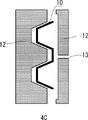
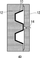
- the second production method of the molded body according to the present embodiment includes a step of producing a molded film by printing the conductive composition for a molded film of the present embodiment on a base film and drying. Forming the molded film into a predetermined shape; Placing the molded film after molding in a mold for injection molding; Forming a base material by injection molding, and integrating the molded film and the base material.
- a description will be given with reference to FIGS. 4A to 4E.
- the second manufacturing method may be referred to as a film insert method.
- FIG. 4A to 4E are schematic process diagrams showing an example of a second manufacturing method of a molded body.
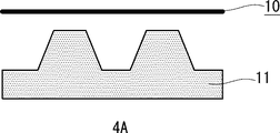
- the molded film 10 is previously molded into a predetermined shape by the mold 11 (FIG. 4A).
- the molded film 10 is molded by the mold 11 after being softened by heating, or while being softened, by performing suction to the mold by vacuum or pressing to the mold by compressed air, or both of them (FIG. 4B).
- the molded film 10 may be molded such that the conductive layer faces the base 20 side to be described later or the side opposite to the base 20 and is selected depending on the use of the final molded body.
- the molded film 10 after molding is placed in a mold 12 for injection molding (FIGS. 4C to 4D).
- the resin is injected 14 from the opening 13 to form the base material 20, and the molded film 10 and the base material 20 are integrated to obtain a molded body 30 (FIG. 4E).
- the base material 20 does not need to be prepared in advance, and the base material can be molded and integrated with the molded film at the same time.
- the material of the base material 20 can be appropriately selected from known resins used for injection molding.
- the third production method of the molded body according to the present embodiment includes a step of producing the molded film by printing the conductive composition for a molded film of the present embodiment on a base film by screen printing and drying. Placing the molded film in a mold for injection molding; And forming a substrate by injection molding and transferring the conductive layer in the molded film to the substrate side.
- a description will be given with reference to FIGS. 5A to 5C.
- the third manufacturing method may be referred to as an in-mold transfer method.
- FIG. 5A to FIG. 5C are schematic process diagrams showing an example of a third manufacturing method of a molded body.
- the molded film 10 is selected and used as a base film having peelability.
- the molding film 10 is placed in the injection mold 12 so that the conductive layer faces the substrate 20 described later (FIG. 5A).
- the resin is injected 14 from the opening 13 to form the base material 20, the molded film 10 and the base material 20 are in close contact, and at least the conductive layer is transferred to the base material 20 side (FIG. 5B).
- a molded body 30 is obtained (FIG. 5C).
- the molded film 10 has a decoration layer, a decoration layer and a conductive layer are transcribe
- a long base film can be arranged as shown in the examples of FIGS. 5A to 5C.
- the material of the base material 20 can be appropriately selected from known resins used for injection molding.
- the molded body thus obtained makes it possible to mount circuits, touch sensors, and various electronic components on plastic housings such as home appliances, automotive parts, robots, and drones. In addition, it is extremely useful for reducing the size and weight of electronic devices, improving the degree of design freedom, and increasing the number of functions.
- the present invention will be described in more detail with reference to examples. However, the following examples do not limit the present invention.
- “part” represents “part by mass”, and “%” represents “mass%”.
- the weight average molecular weight in the examples is a molecular weight in terms of polystyrene in measurement using GPC (gel permeation chromatography) “HLC-8320” manufactured by Tosoh Corporation.
- the functional group value is a general term for an amount expressed as, for example, an acid value when the functional group is a carboxyl group, a hydroxyl value when the functional group is a hydroxy group, and an amine value when the functional group is an amino group.
- the functional groups have the same molar amount if the functional group values are the same.
- the functional group value is, for example, water used for neutralization using a publicly known measurement method defined in JIS K 0070. Measured values (acid value and hydroxyl value) can also be directly determined from an appropriate amount of potassium oxide, and can be handled in the same manner as the calculated value by the above formula.
- the above functional group equivalent and the above calculation formula derived from the respective measured values representing the functional group amount are used. For convenience, it can be calculated as a potassium hydroxide equivalent. A specific calculation example is shown below.
- Amount of isocyanate measured by a method defined in JIS K 6806 (method of reacting an isocyanate group with n-dibutylamine and titrating the remaining n-dibutylamine with aqueous hydrochloric acid) as a compound having an isocyanate group Is calculated for the trifunctional isocyanate compound “X” in which is 23%.
- the reaction was carried out at 240 ° C. for 2 hours, and the acid value was measured.
- the inside of the reactor was gradually reduced to 1 to 2 torr, and when the predetermined viscosity was reached, the reaction was stopped and the surface was removed.
- the polyester resin (A3) containing a weight average molecular weight of 45,000, a glass transition point of 60 ° C., and a hydroxyl group (hydroxyl value of 5 mgKOH / g) in a molecule of 2 or more by transferring to a fluorine-processed pallet and cooling. A solid was obtained.
- ⁇ Production Example 1 Creation of decorative ink (F1)> 175 parts of resin solution (A3) (70 parts as resin (A3) alone) was prepared, and 10 parts of phthalocyanine blue pigment (LIONOL BLUE FG7351 manufactured by Toyocolor Co.) and titanium oxide pigment (TIPAQUE CR-93 manufactured by Ishihara Sangyo Co., Ltd.) were prepared. ) After stirring and mixing 20 parts by mass and kneading with a three roll mill (manufactured by Kodaira Seisakusho), 5 parts of isocyanate curing agent (Desmodule N3300, Sumika Cobestro Urethane Co., Ltd., 100% nonvolatile content) and 90 parts of toluene were added. The decorative ink (F1) was obtained by uniformly stirring and mixing.
- Example 1 Production of conductive composition for molded film (E1)> 20.0 parts of resin (A1) is dissolved in 30.0 parts of solvent (C′1), 80.0 parts of conductive fine particles (B1) are stirred and mixed, and kneaded with a three-roll mill (manufactured by Kodaira Seisakusho). Thus, a conductive composition for molded film (E1) was obtained.
- Example 2 Production of conductive compositions (E2) to (E16) for molded film>
- the types and blending amounts of the resin, solvent, and conductive fine particles were changed as shown in Table 1, and if necessary, molding was performed in the same manner as in Example 1 except that a crosslinking agent was blended.
- Conductive compositions (E2) to (E16) for films were obtained.
- the numerical values of each material in Tables 1 to 4 are parts by mass.
- a polycarbonate (PC) film Teijin, Panlite 2151, thickness 300 ⁇ m
- the conductive compositions for molded film (E1) to (E14) were respectively screen printers (Minoscreen) Manufactured by Minomat SR5575 semi-automatic screen printer).
- a conductive layer having a rectangular solid shape with a width of 15 mm, a length of 30 mm, and a thickness of 10 ⁇ m and a linear pattern with a line width of 3 mm, a length of 60 mm, and a thickness of 10 ⁇ m is heated by heating at 120 ° C. for 30 minutes in a hot air drying oven.
- a molded film provided was obtained.
- Examples 33 to 48 and Comparative Examples 7 to 9> In Examples 17 to 32, instead of the polycarbonate film substrate, an acrylic resin film (Sumitomo Chemical Co., Ltd., Technoloy S001G, thickness 250 ⁇ m) substrate (300 mm ⁇ 210 mm) was used, and in a hot air drying oven A molded film was obtained in the same manner as in Examples 17 to 32 except that the drying conditions were set at 80 ° C. for 30 minutes.
- Example 49 a polycarbonate resin / acrylic resin type 2 two-layer co-extruded film (manufactured by Sumitomo Chemical Co., Ltd., Technoloy C001, thickness 125 ⁇ m) substrate (300 mm ⁇ 210 mm) was used instead of the acrylic resin film substrate.
- a molded film was obtained in the same manner as in Example 33 except that the conductive composition for molded film was printed on the resin side.
- Example 50> A decorative film (F1) is coated on a polycarbonate film (Teijin Ltd., Panlite 2151, thickness 300 ⁇ m) using a blade coater so that the dry film thickness is 2 ⁇ m. The decorative layer was formed by heating at 120 ° C. for 30 minutes.
- a polycarbonate film was obtained in the same manner as in Examples 17 to 32 except that the above-mentioned film with a decorative layer was used instead of the polycarbonate film and a conductive layer was formed on the decorative layer.
- a molded film in which a decorative ink layer and a conductor were laminated in this order was obtained.
- the conductive composition (E1) is formed on a release-treated PET film (Lintec Corp., CN100) substrate by a screen printer (Minoscreen SR Minor SR5575 semi-automatic screen printer) so that the dry film thickness becomes 10 ⁇ m. After being printed on, a conductive layer of a solid conductive composition (E1) was formed by heating at 120 ° C. for 30 minutes in a hot air drying oven. Next, the conductive layer was peeled from the release-treated PET film to obtain a conductive layer for measuring elongation at break.
- a release-treated PET film substrate is prepared, and a decorative ink (F1) is coated on the substrate using a blade coater so that the dry film thickness is 2 ⁇ m, and the temperature is 120 ° C. for 30 minutes. A decorative layer was formed by heating. Next, the decorative layer was peeled from the release-treated PET film to obtain a decorative layer for measuring elongation at break. Moreover, a polycarbonate film (manufactured by Teijin Ltd., Panlite 2151, thickness of 300 ⁇ m) was prepared as a base film for measuring elongation at break.
- the breaking elongation when the conductive layer, the decorative layer, and the base film for measuring the breaking elongation are each cut into a shape of 60 mm ⁇ 10 mm and stretched at a pulling speed of 10 mm / min in a heating oven at 160 ° C. was measured.
- the elongation at break was 400% for the base film, 300% for the decorative layer, and 140% for the conductive layer.
- Example 51 to 53 Production of molded body> A hemispherical ABS resin molding having a radius of 3 cm is aligned so as to face the surface on the conductor side so as to overlap with the position of the linear pattern of 3 mm ⁇ 60 mm of the molded film of Example 11, Example 49 and Example 50, By performing overlay molding at a set temperature of 160 ° C. using a TOM molding machine (manufactured by Fuse Vacuum Co., Ltd.), a molded body in which a molded film molded into a hemispherical shape and an ABS resin molded product were integrated was obtained.
- TOM molding machine manufactured by Fuse Vacuum Co., Ltd.
- the disconnection is not confirmed, and the resistance value variation is 10 times or more and less than 100 times, and is a three-dimensional circuit practical as a circuit. Was confirmed.
- Examples 54 to 56> A hemispherical metal mold having a radius of 3 cm faces the conductor side surface so as to overlap the position of the linear pattern of 3 mm ⁇ 60 mm of the molded film obtained in Example 33, Example 49, and Example 50.
- overlay molding at a set temperature of 160 ° C. using a TOM molding machine (manufactured by Fuse Vacuum Co., Ltd.), a film with a patterned conductor formed into a hemispherical shape was obtained.
- the molded film formed into the hemispherical shape is set in an injection molding machine (IS170 (i5), manufactured by Toshiba Machine Co., Ltd.) to which a valve gate type in-mold test mold is attached, and PC / ABS resin (LUPOYPC / ABSHI5002, LG Chemical Co., Ltd.) was injection molded to obtain a molded body integrated with a film with a patterned conductor (injection conditions: screw diameter 40 mm, cylinder temperature 250 ° C., mold) Temperature (fixed side, movable side) 60 ° C., injection pressure 160 MPa (80%), holding pressure 100 MPa, injection speed 60 mm / second (28%), injection time 4 seconds, cooling time 20 seconds).
- injection molding machine IS170 (i5), manufactured by Toshiba Machine Co., Ltd.
- PC / ABS resin LPOYPC / ABSHI5002, LG Chemical Co., Ltd.
- the disconnection is not confirmed, and the resistance value variation is 10 times or more and less than 100 times, and is a three-dimensional circuit practical as a circuit. Was confirmed.
- the conductive composition of the present embodiment does not cause disconnection or dropout due to the adhesion of the resulting conductive layer and the stretching of the conductive layer during molding, and the resistance value is also excellently increased. It was kept in. This is because the solvent used in the conductive composition of the present embodiment has a high boiling point and a specific HSP range, so that volatilization is slow and good printability can be maintained, and at the time of high temperature contact with the base film. It is presumed that the penetration of the solvent into the substrate was suppressed to the minimum, and good substrate adhesion and cohesive strength, conductivity and stretchability of the conductor were exhibited.
- the molded film and wiring-integrated molded body using the conductive composition of the present embodiment can be directly applied to plastic casings and three-dimensional shaped parts such as home appliances, automotive parts, robots, and drones. It is possible to create lightweight and space-saving circuits without sacrificing damage, touch sensors, antennas, sheet heating elements, electromagnetic wave shields, inductors (coils), resistors, and mounting various electronic components. To. In addition, it is extremely useful for reducing the size and weight of electronic devices, improving the degree of design freedom, and increasing the number of functions.
Abstract
La présente invention concerne une composition conductrice pour un film moulé qui permet la production d'un film moulé pour lequel des réductions de conductivité induites par une force de traction sont supprimées. La composition conductrice pour un film moulé contient une résine (A), de fines particules conductrices (B) et un solvant (C), le solvant (C) contenant, dans 100 parties en masse du solvant (C), au moins 40 parties en masse d'un solvant (C') qui remplit la condition (1) et la condition (2) suivantes. (1) Un point d'ébullition compris entre 180 °C et 270 °C (2) au moins l'une des conditions suivantes est remplie : le paramètre polaire δp du paramètre de solubilité de Hansen (HSP) est 0 ≤ δp ≤ 5,0 et le paramètre de liaison hydrogène δh du paramètre de solubilité de Hansen (HSP) est 9,8 ≤ δh ≤ 24,0.
Priority Applications (3)
| Application Number | Priority Date | Filing Date | Title |
|---|---|---|---|
| CN201980019048.8A CN111868841B (zh) | 2018-04-19 | 2019-04-12 | 成形膜用导电性组合物、成形膜、成形体及其制造方法 |
| EP19787594.1A EP3783625A4 (fr) | 2018-04-19 | 2019-04-12 | Composition conductrice pour un film moulé, film moulé, article moulé et son procédé de production |
| US17/040,045 US20210016541A1 (en) | 2018-04-19 | 2019-04-12 | Conductive composition for molded film, molded film, molded article, and method for production thereof |
Applications Claiming Priority (2)
| Application Number | Priority Date | Filing Date | Title |
|---|---|---|---|
| JP2018-080514 | 2018-04-19 | ||
| JP2018080514A JP6521138B1 (ja) | 2018-04-19 | 2018-04-19 | 成形フィルム用導電性組成物、成形フィルム、成形体およびその製造方法 |
Publications (1)
| Publication Number | Publication Date |
|---|---|
| WO2019203159A1 true WO2019203159A1 (fr) | 2019-10-24 |
Family
ID=66655677
Family Applications (1)
| Application Number | Title | Priority Date | Filing Date |
|---|---|---|---|
| PCT/JP2019/016000 WO2019203159A1 (fr) | 2018-04-19 | 2019-04-12 | Composition conductrice pour un film moulé, film moulé, article moulé et son procédé de production |
Country Status (6)
| Country | Link |
|---|---|
| US (1) | US20210016541A1 (fr) |
| EP (1) | EP3783625A4 (fr) |
| JP (1) | JP6521138B1 (fr) |
| CN (1) | CN111868841B (fr) |
| TW (1) | TWI796472B (fr) |
| WO (1) | WO2019203159A1 (fr) |
Families Citing this family (11)
| Publication number | Priority date | Publication date | Assignee | Title |
|---|---|---|---|---|
| KR20210106424A (ko) | 2019-01-18 | 2021-08-30 | 헨켈 아이피 앤드 홀딩 게엠베하 | 신장성 전기 전도성 잉크 조성물 |
| JP7283284B2 (ja) * | 2019-07-22 | 2023-05-30 | 東洋インキScホールディングス株式会社 | 成形フィルム用導電性組成物、成形フィルムおよびその製造方法、成形体およびその製造方法 |
| JP7222871B2 (ja) * | 2019-11-05 | 2023-02-15 | 大日精化工業株式会社 | 熱硬化性樹脂組成物、塗料、及び積層シート |
| TWI743683B (zh) * | 2020-02-14 | 2021-10-21 | 碩禾電子材料股份有限公司 | 用於hjt太陽能電池的導電漿料、hjt太陽能電池與電極結構 |
| JP6856152B1 (ja) * | 2020-03-06 | 2021-04-07 | 東洋インキScホールディングス株式会社 | 成形フィルム、成形体およびその製造方法 |
| JP7409654B2 (ja) * | 2020-04-17 | 2024-01-09 | 十条ケミカル株式会社 | スクリーン印刷用導電性樹脂組成物、及びプリント配線板 |
| JP7473762B2 (ja) | 2020-06-19 | 2024-04-24 | artience株式会社 | 成形フィルム、成形体およびその製造方法 |
| JPWO2022153925A1 (fr) * | 2021-01-14 | 2022-07-21 | ||
| JP2022152324A (ja) * | 2021-03-29 | 2022-10-12 | 株式会社オートネットワーク技術研究所 | 電装品、及び電装品の製造方法 |
| CN113980604A (zh) * | 2021-10-20 | 2022-01-28 | 江苏尚科聚合新材料有限公司 | 一种兼具安全性的tom膜及其制备方法和应用 |
| JP2024043509A (ja) * | 2022-09-16 | 2024-03-29 | サトーホールディングス株式会社 | 導電性基材の製造方法、電子デバイスの製造方法、電磁波シールドフィルムの製造方法、面状発熱体の製造方法および導電性組成物 |
Citations (13)
| Publication number | Priority date | Publication date | Assignee | Title |
|---|---|---|---|---|
| JPS6110579B2 (fr) * | 1980-09-27 | 1986-03-29 | Tokyo Juki Industrial Co Ltd | |
| JPS6428998A (en) * | 1987-07-24 | 1989-01-31 | Tatsuta Densen Kk | Manufacture of electromagnetic wave shield molding |
| WO2007126012A1 (fr) * | 2006-04-28 | 2007-11-08 | Toyo Ink Mfg. Co., Ltd. | Procede de production d'un film de revetement conducteur |
| JP2007296848A (ja) | 2006-04-06 | 2007-11-15 | Shin Etsu Polymer Co Ltd | 加飾シート及びその製造方法 |
| JP2011057859A (ja) * | 2009-09-10 | 2011-03-24 | Harima Chemicals Inc | 低温硬化可能な導電性ペースト |
| JP2011252140A (ja) | 2010-02-05 | 2011-12-15 | Toyo Ink Sc Holdings Co Ltd | 導電性インキ、および導電パターン付き積層体とその製造方法 |
| JP2012011691A (ja) | 2010-07-01 | 2012-01-19 | Nissha Printing Co Ltd | 導電回路一体化成形品及びその製造方法 |
| JP2012150920A (ja) * | 2011-01-17 | 2012-08-09 | Namics Corp | 導電性組成物及び導電膜 |
| JP2015007230A (ja) * | 2013-06-24 | 2015-01-15 | ゼロックス コーポレイションXerox Corporation | ポリビニルブチラールバインダーを含む導電性金属インク |
| JP2015172103A (ja) * | 2014-03-11 | 2015-10-01 | Dic株式会社 | 導電性インキ組成物、導電性パターンの製造方法及び導電性回路 |
| WO2017163615A1 (fr) * | 2016-03-23 | 2017-09-28 | 昭和電工株式会社 | Résine de liant pour composition conductrice, composition pour formation de motif conducteur contenant celle-ci, et polyuréthane |
| JP2017538247A (ja) * | 2014-10-14 | 2017-12-21 | サン ケミカル コーポレイション | 熱成形可能な導電性インクおよびコーティングならびに熱成形デバイスの製造プロセス |
| JP2018080514A (ja) | 2016-11-17 | 2018-05-24 | 大成建設株式会社 | コンクリート表面形状の品質管理装置 |
Family Cites Families (16)
| Publication number | Priority date | Publication date | Assignee | Title |
|---|---|---|---|---|
| JP2002298648A (ja) * | 2001-04-02 | 2002-10-11 | Mitsubishi Rayon Co Ltd | 導電性光硬化性樹脂組成物、導電性光硬化性シートおよび導電性インサート成形品 |
| JP4971104B2 (ja) * | 2007-11-02 | 2012-07-11 | 住友ゴム工業株式会社 | 導電性ペーストとそれを用いた透光性電磁波シールド板の製造方法 |
| US8765025B2 (en) * | 2010-06-09 | 2014-07-01 | Xerox Corporation | Silver nanoparticle composition comprising solvents with specific hansen solubility parameters |
| WO2012111480A1 (fr) * | 2011-02-16 | 2012-08-23 | 株式会社 村田製作所 | Pâte conductrice et photopile |
| JP5670924B2 (ja) * | 2012-01-10 | 2015-02-18 | 株式会社ノリタケカンパニーリミテド | 導電性接合材とこれを用いたセラミック電子材料の接合方法およびセラミック電子デバイス |
| KR102092990B1 (ko) * | 2012-11-06 | 2020-03-24 | 가부시키가이샤 노리타케 캄파니 리미티드 | 도전성 페이스트 조성물 |
| JP5607187B2 (ja) * | 2013-01-15 | 2014-10-15 | 東海ゴム工業株式会社 | 導電材料、その製造方法、およびそれを用いたトランスデューサ |
| WO2015005204A1 (fr) * | 2013-07-08 | 2015-01-15 | 東洋紡株式会社 | Pâte électroconductrice |
| WO2015111615A1 (fr) * | 2014-01-22 | 2015-07-30 | 東洋紡株式会社 | Pâte conductrice pour gravure au laser, film mince conducteur et stratifié conducteur |
| JP2015193709A (ja) * | 2014-03-31 | 2015-11-05 | 太陽インキ製造株式会社 | 導電性樹脂組成物及び導電回路 |
| JP2018523734A (ja) * | 2015-08-03 | 2018-08-23 | ヘンケル アイピー アンド ホールディング ゲゼルシャフト ミット ベシュレンクテル ハフツング | 高導電性組成物の堆積による電磁干渉シールド保護の達成 |
| WO2017026130A1 (fr) * | 2015-08-07 | 2017-02-16 | 太陽インキ製造株式会社 | Composition conductrice, conducteur et base |
| EP3333225A4 (fr) * | 2015-08-07 | 2019-02-27 | Taiyo Ink Mfg. Co., Ltd. | Composition électroconductrice, conducteur, et carte de circuit imprimé flexible |
| EP3315562B1 (fr) * | 2016-09-02 | 2019-06-26 | Teikoku Printing Inks Mfg. Co., Ltd | Composition liquide électroconductrice |
| CN107828351B (zh) * | 2016-09-15 | 2021-07-27 | E·I·内穆尔杜邦公司 | 用于粘合的导电糊料 |
| KR20200043969A (ko) * | 2017-08-24 | 2020-04-28 | 도요보 가부시키가이샤 | 도전성 페이스트, 입체 인쇄 회로, 터치 센서 및 이들의 제법 |
-
2018
- 2018-04-19 JP JP2018080514A patent/JP6521138B1/ja active Active
-
2019
- 2019-04-12 CN CN201980019048.8A patent/CN111868841B/zh active Active
- 2019-04-12 EP EP19787594.1A patent/EP3783625A4/fr active Pending
- 2019-04-12 WO PCT/JP2019/016000 patent/WO2019203159A1/fr active Application Filing
- 2019-04-12 US US17/040,045 patent/US20210016541A1/en active Pending
- 2019-04-18 TW TW108113617A patent/TWI796472B/zh active
Patent Citations (13)
| Publication number | Priority date | Publication date | Assignee | Title |
|---|---|---|---|---|
| JPS6110579B2 (fr) * | 1980-09-27 | 1986-03-29 | Tokyo Juki Industrial Co Ltd | |
| JPS6428998A (en) * | 1987-07-24 | 1989-01-31 | Tatsuta Densen Kk | Manufacture of electromagnetic wave shield molding |
| JP2007296848A (ja) | 2006-04-06 | 2007-11-15 | Shin Etsu Polymer Co Ltd | 加飾シート及びその製造方法 |
| WO2007126012A1 (fr) * | 2006-04-28 | 2007-11-08 | Toyo Ink Mfg. Co., Ltd. | Procede de production d'un film de revetement conducteur |
| JP2011057859A (ja) * | 2009-09-10 | 2011-03-24 | Harima Chemicals Inc | 低温硬化可能な導電性ペースト |
| JP2011252140A (ja) | 2010-02-05 | 2011-12-15 | Toyo Ink Sc Holdings Co Ltd | 導電性インキ、および導電パターン付き積層体とその製造方法 |
| JP2012011691A (ja) | 2010-07-01 | 2012-01-19 | Nissha Printing Co Ltd | 導電回路一体化成形品及びその製造方法 |
| JP2012150920A (ja) * | 2011-01-17 | 2012-08-09 | Namics Corp | 導電性組成物及び導電膜 |
| JP2015007230A (ja) * | 2013-06-24 | 2015-01-15 | ゼロックス コーポレイションXerox Corporation | ポリビニルブチラールバインダーを含む導電性金属インク |
| JP2015172103A (ja) * | 2014-03-11 | 2015-10-01 | Dic株式会社 | 導電性インキ組成物、導電性パターンの製造方法及び導電性回路 |
| JP2017538247A (ja) * | 2014-10-14 | 2017-12-21 | サン ケミカル コーポレイション | 熱成形可能な導電性インクおよびコーティングならびに熱成形デバイスの製造プロセス |
| WO2017163615A1 (fr) * | 2016-03-23 | 2017-09-28 | 昭和電工株式会社 | Résine de liant pour composition conductrice, composition pour formation de motif conducteur contenant celle-ci, et polyuréthane |
| JP2018080514A (ja) | 2016-11-17 | 2018-05-24 | 大成建設株式会社 | コンクリート表面形状の品質管理装置 |
Non-Patent Citations (2)
| Title |
|---|
| JISM8511, 2014 |
| See also references of EP3783625A4 |
Also Published As
| Publication number | Publication date |
|---|---|
| JP2019189680A (ja) | 2019-10-31 |
| US20210016541A1 (en) | 2021-01-21 |
| JP6521138B1 (ja) | 2019-05-29 |
| CN111868841A (zh) | 2020-10-30 |
| CN111868841B (zh) | 2023-01-24 |
| TWI796472B (zh) | 2023-03-21 |
| EP3783625A1 (fr) | 2021-02-24 |
| EP3783625A4 (fr) | 2022-01-19 |
| TW201943809A (zh) | 2019-11-16 |
Similar Documents
| Publication | Publication Date | Title |
|---|---|---|
| WO2019203159A1 (fr) | Composition conductrice pour un film moulé, film moulé, article moulé et son procédé de production | |
| US11139089B2 (en) | Stretchable interconnects for flexible electronic surfaces | |
| JP7279510B2 (ja) | 成形フィルム用導電性組成物、成形フィルムおよびその製造方法、成形体およびその製造方法 | |
| TWI732839B (zh) | 延展性導電糊劑及曲面印刷電路板之製造方法 | |
| US20110088931A1 (en) | Multilayer Coatings and Coated Articles | |
| US20110086206A1 (en) | Polymer compositions containing carbonaceous fillers | |
| KR20120107044A (ko) | 그라핀 시트 및 흑연을 함유하는 중합체 조성물 | |
| JP2023021155A (ja) | 導電性ペースト、立体印刷回路、タッチセンサーおよびそれらの製法 | |
| CN110027268A (zh) | 电磁波屏蔽膜 | |
| JP2020011502A (ja) | 成形フィルムおよびその製造方法、成形体およびその製造方法 | |
| JP7283284B2 (ja) | 成形フィルム用導電性組成物、成形フィルムおよびその製造方法、成形体およびその製造方法 | |
| KR20160032302A (ko) | 플렉서블 투명전극용 다층시트 및 그 제조방법 | |
| JP7118582B2 (ja) | 展延性導電性組成物および三次元プリント配線板の製造方法 | |
| JP6856152B1 (ja) | 成形フィルム、成形体およびその製造方法 | |
| JP7473761B2 (ja) | 成形フィルムおよびその製造方法、成形体およびその製造方法 | |
| JP7473762B2 (ja) | 成形フィルム、成形体およびその製造方法 | |
| JP2022065264A (ja) | 成形フィルム、成形体およびその製造方法 | |
| JP2020002343A (ja) | 成形フィルム用導電性組成物、成形フィルムおよびその製造方法、成形体およびその製造方法 | |
| JP2022055394A (ja) | 成形フィルム、成形体およびその製造方法 | |
| JP2023005666A (ja) | 成形フィルム用導電性組成物、成形フィルムおよびその製造方法、成形体およびその製造方法 | |
| JP2022037748A (ja) | 成形フィルム用導電性組成物、成形フィルムおよびその製造方法、成形体およびその製造方法 | |
| JP2023076844A (ja) | 成形体およびその製造方法 | |
| JP2022088712A (ja) | 成形フィルム用導電性組成物、成形フィルム、及びその製造方法、並びに、成形体及びその製造方法 | |
| JP2024029494A (ja) | 成形フィルム用導電性組成物、成形フィルムおよびその製造方法、成形体およびその製造方法 |
Legal Events
| Date | Code | Title | Description |
|---|---|---|---|
| 121 | Ep: the epo has been informed by wipo that ep was designated in this application |
Ref document number: 19787594 Country of ref document: EP Kind code of ref document: A1 |
|
| NENP | Non-entry into the national phase |
Ref country code: DE |
|
| WWE | Wipo information: entry into national phase |
Ref document number: 2019787594 Country of ref document: EP |
|
| ENP | Entry into the national phase |
Ref document number: 2019787594 Country of ref document: EP Effective date: 20201119 |