WO2019181825A1 - カメラモジュール - Google Patents
カメラモジュール Download PDFInfo
- Publication number
- WO2019181825A1 WO2019181825A1 PCT/JP2019/011077 JP2019011077W WO2019181825A1 WO 2019181825 A1 WO2019181825 A1 WO 2019181825A1 JP 2019011077 W JP2019011077 W JP 2019011077W WO 2019181825 A1 WO2019181825 A1 WO 2019181825A1
- Authority
- WO
- WIPO (PCT)
- Prior art keywords
- terminal
- flexible substrate
- electronic component
- rear surface
- camera module
- Prior art date
Links
- 239000000758 substrate Substances 0.000 claims abstract description 193
- 238000003384 imaging method Methods 0.000 claims abstract description 17
- 238000012545 processing Methods 0.000 claims description 58
- 239000004020 conductor Substances 0.000 claims description 32
- 239000000463 material Substances 0.000 claims description 21
- 238000005452 bending Methods 0.000 claims description 17
- 238000000034 method Methods 0.000 claims description 14
- 230000008569 process Effects 0.000 claims description 8
- 239000010410 layer Substances 0.000 description 35
- 230000000694 effects Effects 0.000 description 17
- 230000003287 optical effect Effects 0.000 description 15
- 230000002093 peripheral effect Effects 0.000 description 13
- 229910000679 solder Inorganic materials 0.000 description 9
- 239000002184 metal Substances 0.000 description 7
- 239000000853 adhesive Substances 0.000 description 6
- 230000001070 adhesive effect Effects 0.000 description 6
- 239000012212 insulator Substances 0.000 description 5
- 239000003990 capacitor Substances 0.000 description 4
- 238000006243 chemical reaction Methods 0.000 description 4
- 239000011347 resin Substances 0.000 description 4
- 229920005989 resin Polymers 0.000 description 4
- 206010040844 Skin exfoliation Diseases 0.000 description 3
- 230000005540 biological transmission Effects 0.000 description 3
- 238000013461 design Methods 0.000 description 3
- 238000010586 diagram Methods 0.000 description 3
- 239000006185 dispersion Substances 0.000 description 3
- 239000004519 grease Substances 0.000 description 3
- 239000011810 insulating material Substances 0.000 description 3
- 230000005855 radiation Effects 0.000 description 3
- 239000012790 adhesive layer Substances 0.000 description 2
- 230000000903 blocking effect Effects 0.000 description 2
- 239000000919 ceramic Substances 0.000 description 2
- 238000007667 floating Methods 0.000 description 2
- 230000013011 mating Effects 0.000 description 2
- 230000009467 reduction Effects 0.000 description 2
- 230000001105 regulatory effect Effects 0.000 description 2
- 230000003321 amplification Effects 0.000 description 1
- 230000008859 change Effects 0.000 description 1
- 230000000295 complement effect Effects 0.000 description 1
- 230000008602 contraction Effects 0.000 description 1
- 230000001276 controlling effect Effects 0.000 description 1
- 238000013016 damping Methods 0.000 description 1
- 238000011161 development Methods 0.000 description 1
- 238000006073 displacement reaction Methods 0.000 description 1
- 238000005516 engineering process Methods 0.000 description 1
- 239000004744 fabric Substances 0.000 description 1
- 238000001914 filtration Methods 0.000 description 1
- 239000011521 glass Substances 0.000 description 1
- 230000017525 heat dissipation Effects 0.000 description 1
- 230000020169 heat generation Effects 0.000 description 1
- 238000003780 insertion Methods 0.000 description 1
- 230000037431 insertion Effects 0.000 description 1
- 238000003199 nucleic acid amplification method Methods 0.000 description 1
- 239000003973 paint Substances 0.000 description 1
- 238000003825 pressing Methods 0.000 description 1
- 239000004065 semiconductor Substances 0.000 description 1
- 238000000926 separation method Methods 0.000 description 1
- 230000008054 signal transmission Effects 0.000 description 1
- 230000011664 signaling Effects 0.000 description 1
- 239000007787 solid Substances 0.000 description 1
- 238000012546 transfer Methods 0.000 description 1
- 230000007704 transition Effects 0.000 description 1
Images


Classifications
-
- H—ELECTRICITY
- H04—ELECTRIC COMMUNICATION TECHNIQUE
- H04N—PICTORIAL COMMUNICATION, e.g. TELEVISION
- H04N23/00—Cameras or camera modules comprising electronic image sensors; Control thereof
- H04N23/50—Constructional details
- H04N23/51—Housings
-
- G—PHYSICS
- G03—PHOTOGRAPHY; CINEMATOGRAPHY; ANALOGOUS TECHNIQUES USING WAVES OTHER THAN OPTICAL WAVES; ELECTROGRAPHY; HOLOGRAPHY
- G03B—APPARATUS OR ARRANGEMENTS FOR TAKING PHOTOGRAPHS OR FOR PROJECTING OR VIEWING THEM; APPARATUS OR ARRANGEMENTS EMPLOYING ANALOGOUS TECHNIQUES USING WAVES OTHER THAN OPTICAL WAVES; ACCESSORIES THEREFOR
- G03B17/00—Details of cameras or camera bodies; Accessories therefor
- G03B17/02—Bodies
-
- H—ELECTRICITY
- H01—ELECTRIC ELEMENTS
- H01L—SEMICONDUCTOR DEVICES NOT COVERED BY CLASS H10
- H01L27/00—Devices consisting of a plurality of semiconductor or other solid-state components formed in or on a common substrate
- H01L27/14—Devices consisting of a plurality of semiconductor or other solid-state components formed in or on a common substrate including semiconductor components sensitive to infrared radiation, light, electromagnetic radiation of shorter wavelength or corpuscular radiation and specially adapted either for the conversion of the energy of such radiation into electrical energy or for the control of electrical energy by such radiation
- H01L27/144—Devices controlled by radiation
- H01L27/146—Imager structures
- H01L27/14601—Structural or functional details thereof
- H01L27/14618—Containers
-
- H—ELECTRICITY
- H04—ELECTRIC COMMUNICATION TECHNIQUE
- H04N—PICTORIAL COMMUNICATION, e.g. TELEVISION
- H04N23/00—Cameras or camera modules comprising electronic image sensors; Control thereof
- H04N23/50—Constructional details
- H04N23/54—Mounting of pick-up tubes, electronic image sensors, deviation or focusing coils
-
- H—ELECTRICITY
- H04—ELECTRIC COMMUNICATION TECHNIQUE
- H04N—PICTORIAL COMMUNICATION, e.g. TELEVISION
- H04N23/00—Cameras or camera modules comprising electronic image sensors; Control thereof
- H04N23/50—Constructional details
- H04N23/55—Optical parts specially adapted for electronic image sensors; Mounting thereof
-
- H—ELECTRICITY
- H04—ELECTRIC COMMUNICATION TECHNIQUE
- H04N—PICTORIAL COMMUNICATION, e.g. TELEVISION
- H04N23/00—Cameras or camera modules comprising electronic image sensors; Control thereof
- H04N23/57—Mechanical or electrical details of cameras or camera modules specially adapted for being embedded in other devices
-
- H—ELECTRICITY
- H05—ELECTRIC TECHNIQUES NOT OTHERWISE PROVIDED FOR
- H05K—PRINTED CIRCUITS; CASINGS OR CONSTRUCTIONAL DETAILS OF ELECTRIC APPARATUS; MANUFACTURE OF ASSEMBLAGES OF ELECTRICAL COMPONENTS
- H05K1/00—Printed circuits
- H05K1/02—Details
- H05K1/0277—Bendability or stretchability details
- H05K1/028—Bending or folding regions of flexible printed circuits
-
- H—ELECTRICITY
- H05—ELECTRIC TECHNIQUES NOT OTHERWISE PROVIDED FOR
- H05K—PRINTED CIRCUITS; CASINGS OR CONSTRUCTIONAL DETAILS OF ELECTRIC APPARATUS; MANUFACTURE OF ASSEMBLAGES OF ELECTRICAL COMPONENTS
- H05K1/00—Printed circuits
- H05K1/02—Details
- H05K1/14—Structural association of two or more printed circuits
- H05K1/147—Structural association of two or more printed circuits at least one of the printed circuits being bent or folded, e.g. by using a flexible printed circuit
-
- H—ELECTRICITY
- H05—ELECTRIC TECHNIQUES NOT OTHERWISE PROVIDED FOR
- H05K—PRINTED CIRCUITS; CASINGS OR CONSTRUCTIONAL DETAILS OF ELECTRIC APPARATUS; MANUFACTURE OF ASSEMBLAGES OF ELECTRICAL COMPONENTS
- H05K1/00—Printed circuits
- H05K1/18—Printed circuits structurally associated with non-printed electric components
- H05K1/189—Printed circuits structurally associated with non-printed electric components characterised by the use of a flexible or folded printed circuit
-
- H—ELECTRICITY
- H05—ELECTRIC TECHNIQUES NOT OTHERWISE PROVIDED FOR
- H05K—PRINTED CIRCUITS; CASINGS OR CONSTRUCTIONAL DETAILS OF ELECTRIC APPARATUS; MANUFACTURE OF ASSEMBLAGES OF ELECTRICAL COMPONENTS
- H05K1/00—Printed circuits
- H05K1/02—Details
- H05K1/11—Printed elements for providing electric connections to or between printed circuits
- H05K1/111—Pads for surface mounting, e.g. lay-out
- H05K1/112—Pads for surface mounting, e.g. lay-out directly combined with via connections
- H05K1/113—Via provided in pad; Pad over filled via
-
- H—ELECTRICITY
- H05—ELECTRIC TECHNIQUES NOT OTHERWISE PROVIDED FOR
- H05K—PRINTED CIRCUITS; CASINGS OR CONSTRUCTIONAL DETAILS OF ELECTRIC APPARATUS; MANUFACTURE OF ASSEMBLAGES OF ELECTRICAL COMPONENTS
- H05K1/00—Printed circuits
- H05K1/18—Printed circuits structurally associated with non-printed electric components
- H05K1/181—Printed circuits structurally associated with non-printed electric components associated with surface mounted components
-
- H—ELECTRICITY
- H05—ELECTRIC TECHNIQUES NOT OTHERWISE PROVIDED FOR
- H05K—PRINTED CIRCUITS; CASINGS OR CONSTRUCTIONAL DETAILS OF ELECTRIC APPARATUS; MANUFACTURE OF ASSEMBLAGES OF ELECTRICAL COMPONENTS
- H05K2201/00—Indexing scheme relating to printed circuits covered by H05K1/00
- H05K2201/05—Flexible printed circuits [FPCs]
- H05K2201/052—Branched
-
- H—ELECTRICITY
- H05—ELECTRIC TECHNIQUES NOT OTHERWISE PROVIDED FOR
- H05K—PRINTED CIRCUITS; CASINGS OR CONSTRUCTIONAL DETAILS OF ELECTRIC APPARATUS; MANUFACTURE OF ASSEMBLAGES OF ELECTRICAL COMPONENTS
- H05K2201/00—Indexing scheme relating to printed circuits covered by H05K1/00
- H05K2201/10—Details of components or other objects attached to or integrated in a printed circuit board
- H05K2201/10007—Types of components
- H05K2201/10121—Optical component, e.g. opto-electronic component
-
- H—ELECTRICITY
- H05—ELECTRIC TECHNIQUES NOT OTHERWISE PROVIDED FOR
- H05K—PRINTED CIRCUITS; CASINGS OR CONSTRUCTIONAL DETAILS OF ELECTRIC APPARATUS; MANUFACTURE OF ASSEMBLAGES OF ELECTRICAL COMPONENTS
- H05K2201/00—Indexing scheme relating to printed circuits covered by H05K1/00
- H05K2201/10—Details of components or other objects attached to or integrated in a printed circuit board
- H05K2201/10007—Types of components
- H05K2201/10151—Sensor
-
- H—ELECTRICITY
- H05—ELECTRIC TECHNIQUES NOT OTHERWISE PROVIDED FOR
- H05K—PRINTED CIRCUITS; CASINGS OR CONSTRUCTIONAL DETAILS OF ELECTRIC APPARATUS; MANUFACTURE OF ASSEMBLAGES OF ELECTRICAL COMPONENTS
- H05K2201/00—Indexing scheme relating to printed circuits covered by H05K1/00
- H05K2201/10—Details of components or other objects attached to or integrated in a printed circuit board
- H05K2201/10227—Other objects, e.g. metallic pieces
- H05K2201/10295—Metallic connector elements partly mounted in a hole of the PCB
- H05K2201/10303—Pin-in-hole mounted pins
-
- H—ELECTRICITY
- H05—ELECTRIC TECHNIQUES NOT OTHERWISE PROVIDED FOR
- H05K—PRINTED CIRCUITS; CASINGS OR CONSTRUCTIONAL DETAILS OF ELECTRIC APPARATUS; MANUFACTURE OF ASSEMBLAGES OF ELECTRICAL COMPONENTS
- H05K3/00—Apparatus or processes for manufacturing printed circuits
- H05K3/0058—Laminating printed circuit boards onto other substrates, e.g. metallic substrates
- H05K3/0064—Laminating printed circuit boards onto other substrates, e.g. metallic substrates onto a polymeric substrate
Definitions
- This disclosure relates to a camera module.
- a camera module that is used as a system element, such as an in-vehicle camera module, is known (for example, Patent Document 1).
- the camera module of Patent Document 1 includes a housing, a lens exposed on the front surface of the housing, and a terminal for external connection exposed on the rear surface of the housing. Inside the housing, in order from the lens side to the terminal side, an image sensor, a rigid first circuit board on which the image sensor is mounted, and a rigid second circuit connected to the first circuit board.
- a flexible substrate that connects the circuit board, the second circuit board, and the terminals is provided.
- a circuit chip (electronic component) is mounted on the second circuit board.
- the flexible substrate has a signal line pattern portion that connects the second substrate and the terminal, and a GND line pattern portion that is branched with respect to the signal line pattern portion.
- the GND line pattern portion is connected to a shield case in the housing.
- the camera module includes a housing, a lens, an assembly, a terminal, a flexible substrate, and an electronic component.
- the housing includes a front surface portion, a rear surface portion on the opposite side, and a side surface portion connecting the front surface portion and the rear surface portion.
- the lens is exposed from the front portion.
- the assembly includes an image sensor and is located on the rear surface side with respect to the lens.
- the terminal is for connection with the outside, located on the rear surface portion.
- the flexible substrate includes a portion extending from the assembly to the terminal.
- the electronic component is mounted on the flexible substrate.
- the camera module includes a housing, a lens, an assembly, a terminal, a connection member, and an electronic component.
- the housing includes a front surface portion, a rear surface portion on the opposite side, and a side surface portion connecting the front surface portion and the rear surface portion.
- the lens is exposed from the front portion.
- the assembly includes an image sensor and is located on the rear surface side with respect to the lens.
- the terminal is for connection with the outside, located on the rear surface portion.
- the connecting member is flexible and extends from the assembly to the terminal.
- the electronic component is electrically connected to the assembly and the terminal, and is located in the casing away from the assembly on the rear surface side.
- the block diagram which shows the structure of the signal processing system of the camera module of FIG. The typical perspective view which fractures
- 9A, 9B, and 9C are a cross-sectional view, a top view, and a bottom view showing an example of a flexible substrate having a reference potential layer.
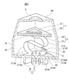
- FIG. 1 is a schematic perspective view showing the camera module 1 according to the first embodiment in a cutaway manner.
- the camera module 1 is for in-vehicle use, for example, and is used for driving support and / or driving records.
- the camera module 1 has vertical, horizontal, and height dimensions of 1 cm or more and 5 cm or less, and is provided inside or outside the vehicle body so as to capture the front, rear, or side of the vehicle body.
- the camera module 1 is electrically connected to an ECU (Electronic Control Unit or Engine Control Unit) (not shown), controlled by the ECU, and a signal output from the camera module 1 is processed by the ECU.
- ECU Electronic Control Unit or Engine Control Unit
- the use of the camera module 1 is not limited to in-vehicle use, and the dimensions thereof may be smaller or larger than the dimensions exemplified above. However, below, the case where the camera module 1 is a vehicle-mounted one may be described as an example.
- the camera module 1 has, for example, a housing 3, a lens 5 exposed from the housing 3, and a plurality of terminals 7 for external connection located on the opposite side of the lens 5 of the housing 3. is doing. As understood from the position of the lens 5, the camera module 1 uses the upper side of the drawing as the imaging side. Further, the vertical direction of the drawing is the optical axis direction.
- the plurality of terminals 7 are connected to the ECU via a cable (not shown) when the camera module 1 is a vehicle-mounted one.
- the camera module 1 also includes an assembly 11 including an image sensor 9, a flexible board 13 extending from the assembly 11 to the plurality of terminals 7, and an electronic component 15 mounted on the flexible board 13. And have. As a result, for example, an image formed by the lens 5 on the image sensor 9 is converted into an electrical signal and output from one of the plurality of terminals 7.
- the camera module 1 may have, for example, a shield case in addition to the above.
- the signal output from the camera module 1 is, for example, a signal including information (image data) for reproducing a captured image.
- the camera module 1 contributes to providing moving image information by sequentially outputting, for example, signals of a plurality of image data (a plurality of frames of image data) obtained over time. Note that the camera module 1 may be used for a purpose of acquiring a still image as necessary. In addition to or instead of the image data signal, the camera module 1 may output information on some determination result based on the image data.
- the housing 3 includes, for example, a portion that holds the lens 5 (front surface portion 3a, lens barrel), a portion that houses the assembly 11 and the like, and a portion that constitutes the connector 17 (connector housing portion 3f).
- the term “casing” indicates not only a pure box-shaped portion but also a relatively wide portion.
- the inside of the housing 3 is basically sealed, for example.
- the outer shape of the housing 3 may be an appropriate shape.
- the outer shape of the housing 3 is roughly a combination of a right prism having a square bottom surface (terminal 7 side) and a frustum having a square bottom surface (lens 5 side).
- the housing 3 has a substantially rectangular outer shape when viewed in the optical axis direction.
- FIG. 1 is a schematic perspective view broken along one diagonal of the rectangle.
- the connector housing portion 3 f is formed in a cylindrical shape that protrudes so as to surround the plurality of terminals 7.
- the cylinder here may be circular or rectangular when viewed in the connecting direction (here, the same direction as the optical axis direction).
- the outer shape of the housing 3 is not limited to the above shape.
- the schematic shape of the outer shape of the housing 3 may be a rectangular parallelepiped, or may be a combination of a rectangular parallelepiped (terminal 7 side) and a column (lens 5 side) protruding from the rectangular parallelepiped, It may be a right prism whose bottom surface is a polygon other than a rectangle (for example, a pentagon), or a combination of such a right prism (terminal 7 side) and a cylinder protruding from the right prism (lens 5 side). It may be a cylinder or a shape with higher design. Each cylinder mentioned above may be a portion that is a lens barrel that holds the lens 5.
- the outer shape of the housing 3 includes a rectangular parallelepiped or right-angled columnar portion on the terminal 7 side as in the illustrated example may be described as an example.
- the shape of the internal space of the housing 3 may be an appropriate shape.
- the shape of the internal space of the housing 3 is generally similar to the outer shape of the housing 3 described above. Therefore, the housing 3 has a substantially rectangular parallelepiped space at least on the terminal 7 side. From another viewpoint, the housing 3 has, on the terminal 7 side, a planar inner surface (the inner surface of the rear surface portion 3b) orthogonal to the optical axis and a planar wall surface (the inner surface of the side surface portion 3d) that surrounds the four sides. is doing.
- the shape of the internal space of the housing 3 is not limited to the above shape, and may be a shape including a polygonal column or a column other than a square column on the terminal 7 side, for example.
- a case where a substantially rectangular parallelepiped space is formed on the terminal 7 side may be described as an example.
- the case 3 includes a front surface portion 3a facing the imaging side (front side of the lens 5), a rear surface portion 3b on the opposite side, a front surface portion 3a and a rear surface. It has the outer peripheral surface part 3c (side surface part 3d) which connects the surface part 3b.
- the outer peripheral surface portion 3c is a portion that connects the front surface portion 3a and the rear surface portion 3b over the entire periphery.
- a portion that becomes a polygonal side when viewed in the optical axis direction is referred to as a side surface portion 3d.
- the outer peripheral surface portion 3c has four side surface portions 3d because the outer shape of the housing 3 includes a right-angled columnar portion at least on the terminal 7 side.
- the shape of the outer surface of each of these portions (3a to 3d) may be an appropriate shape.
- the outer surface of the front surface portion 3a constitutes the upper base of the frustum.
- the outer surface of the rear surface portion 3b constitutes the bottom surface of the right prism (terminal 7 side).
- the outer surface of the outer peripheral surface portion 3c (side surface portion 3d) constitutes the side surface of the frustum and the side surface of the right prism.
- each part (3a-3d) may be defined suitably.
- the outer shape of the housing 3 is a combination of a rectangular parallelepiped (terminal 7 side) and a cylinder protruding from the rectangular parallelepiped (lens 5 side)
- the front surface portion 3a has a cylindrical lens 5 It may be defined as a portion constituting the bottom surface on the side, or may be defined as a portion constituting the entire cylinder and the plane on the cylinder side of the rectangular parallelepiped.
- each part (3a to 3d) may be appropriately set so as to realize the shape of the outer surface and the inner surface of the casing 3 described above.
- each of the front surface portion 3a, the rear surface portion 3b, and the outer peripheral surface portion 3c is roughly formed in a plate shape having a substantially constant thickness with the direction of the outer surface facing the thickness direction.
- the plate shape here includes not only a flat plate shape (example shown in the figure) but also a curved plate shape (for example, a plate shape constituting a cylinder).
- each part (3a to 3d) is not limited to a plate shape whose thickness direction is the direction in which the outer surface of each part faces as described above.
- the housing 3 may include a cylindrical portion around the optical axis (a lens barrel that holds the lens 5), and the front surface portion 3a may be a tip portion (an edge portion of the tube) of the cylindrical portion.
- the housing 3 is configured by combining a plurality of members, for example.
- the division position of the housing 3 (the position of the boundary between the plurality of members), the number of the plurality of members, and the like may be set as appropriate.
- the housing 3 includes a front housing 19 on the lens 5 side and a rear housing 21 on the opposite side.
- the front housing 19 is a box-shaped member whose side opposite to the lens 5 is opened (the box is not limited to a rectangular parallelepiped shape; the same applies hereinafter).
- the rear housing 21 is a box-shaped member with the lens 5 side opened.
- casing 3 is comprised by connecting both the open sides. The two may be connected by various known methods such as engagement, screwing, and adhesion. One open side edge may be fitted inside the other open side edge.
- each of the front housing 19 and the rear housing 21 may be configured by a plurality of members.
- the front housing 19 may be configured such that a lens barrel that holds the lens 5 and a member that forms at least the lens 5 side portion of the outer peripheral surface portion 3c are fixed to each other. This fixing may be performed indirectly through another member in the housing 3.
- the rear housing 21 is configured such that a member constituting a portion other than the connector housing portion 3f of the rear housing 21 and a member constituting the connector housing portion 3f are fixed to each other. Also good.
- the material of the housing 3 is basically an insulating material, for example.
- the insulating material is, for example, a resin. Other insulating materials such as ceramic may be used.
- the housing 3 may be partially or entirely made of a conductor (metal).
- the housing 3 may be one in which a metal (shield case) is embedded in a resin, or basically made of a resin, and a conductive paint is applied to an appropriate position on the inner surface. May be.
- the lens 5 may be a single lens composed of a single lens or a lens group (optical system) composed of a plurality of lenses.
- the lens 5 is disposed in an opening formed in the front surface portion 3 a and is exposed to the outside of the housing 3.
- the lens 5 collects light from the outside of the housing 3 and forms an image inside the housing 3 (on the image sensor 9).
- the lens 5 may be covered with a transparent cover that constitutes a part of the housing 3. Note that the transparent cover can be regarded as a part of the lens 5.
- the terminal 7 is made of, for example, a pin-shaped metal. Each terminal 7 is inserted through a hole formed in the rear surface portion 3b, for example, and is fixed to the rear surface portion 3b with a bonding material such as solder. The plurality of terminals 7 are inserted through holes formed in the flexible substrate 13, for example, and are bonded to the wiring (conductive pattern) of the flexible substrate 13 by a conductive bonding material such as solder.
- the bonding material for bonding the terminal 7 to the rear surface portion 3b and the bonding material for bonding the terminal 7 to the flexible substrate 13 may be different materials or the same material. In the latter case, both may be supplied and cured separately or supplied and cured at the same time.
- the number and arrangement of the terminals 7 may be set as appropriate. In the illustrated example, six terminals 7 are arranged on the center side of the rear surface portion 3b (half of which are shown). The six terminals 7 are arranged in two rows along the side of the rear surface portion 3b.
- the plurality of terminals 7 and the connector casing 3 f constitute a connector 17.
- a mating connector (not shown) that fits in the connector housing 3 f is connected to the connector 17.
- the mating connector has a hole portion into which the pin-shaped terminal 7 is fitted, and a terminal that contacts the terminal 7 is provided on the inner surface of the hole portion.
- the male mold and female mold may be the reverse of the above. That is, the terminal 7 may be formed on the inner surface of the hole through which the pin is inserted.
- the terminal 7 may be a metal member having an appropriate shape that comes into contact with the outer peripheral surface of the pin, for example.
- the shape of the metal member may be, for example, a flat plate shape, a cylindrical shape through which a pin is inserted, or a shape including a leaf spring portion.
- the assembly 11 includes, for example, the above-described imaging element 9 and a rigid substrate 23 on which the imaging element 9 is mounted.
- the image sensor 9 is constituted by a solid-state image sensor such as a CMOS (Complementary Metal-Oxide-Semiconductor) or a CCD (Charge-Coupled Device).
- CMOS Complementary Metal-Oxide-Semiconductor
- CCD Charge-Coupled Device
- the image sensor 9 has a plurality of pixels arranged vertically and horizontally on the light receiving surface on the lens 5 side.
- Each pixel is configured to include a photoelectric conversion element, and converts the light incident on each pixel into an electric signal having a signal intensity corresponding to the amount of light, and outputs the electrical signal.
- image data raw data
- the imaging device 9 includes, for example, a bare chip, a package that seals the bare chip, and a plurality of leads that extend outward and downward from the package. Then, the image pickup device 9 is surface-mounted on the rigid substrate 23 by bonding the lead to the pad-shaped land on the rigid substrate 23 with solder or the like.
- the imaging element 9 may be a mounting method other than the above, or may be a bare chip.
- the image sensor 9 may include, for example, a color filter and / or a lens array.
- the rigid substrate 23 contributes to, for example, fixing (positioning) the imaging element 9 to the housing 3 (lens 5), mounting electronic components (not shown), and the like.
- the image pickup device 9 is electrically connected to another electronic component connected to the rigid board 23 and / or the flexible board 13 via the rigid board 23.
- the rigid board 23 is, for example, a rigid printed wiring board.
- the rigid substrate 23 is, for example, a double-sided board in which a conductor layer is formed on both sides of a plate-like insulator, or a multilayer board in which three or more conductor layers are formed on a plate-like insulator.
- the rigid substrate 23 may be a single-sided plate in which a conductor layer is formed only on one side of a plate-like insulator.
- the planar shape of the rigid substrate 23, the material of the insulator, the material of the conductor layer, the conductor pattern included in the conductor layer, and the like may be appropriate.
- the insulator may be a glass cloth or other base material impregnated with a resin, or may be ceramic.
- the conductor layer may constitute a component such as an inductor or a capacitor in addition to a land for mounting an electronic component and a wiring for connecting the lands.
- the rigid substrate 23 may have an insulating film (solder resist) that covers the conductor layer in order to reduce unnecessary short circuit of the conductor layer.
- the rigid substrate 23 (imaging device 9) is disposed to face the lens 5.
- the rigid substrate 23 is disposed so that the light receiving surface of the image sensor 9 is positioned substantially at the rear focal point of the lens 5.
- the size of the space on the terminal 7 side of the housing 3 relative to the rigid board 23 may be appropriate.
- the distance from the rigid substrate 23 to the inner surface of the rear surface portion 3b (the height of the space on the terminal 7 side) may be longer than the distance from the lens 5 to the image sensor 9.
- the rigid substrate 23 may be fixed to the housing 3 as appropriate.
- the housing 3 has a plurality of rods extending from the front surface portion 3a to the terminal 7 side.
- the rigid substrate 23 has a plurality of holes through which the rods are inserted.
- the rigid substrate 23 is fixed to the housing 3 by mounting rods through a plurality of holes after electronic components such as the image sensor 9 are mounted and joining the rods with a bonding material such as solder. Is done.
- the lens 5 side surface of the rigid substrate 23 may be bonded to the end surface on the terminal 7 side of the member including the lens barrel holding the lens 5.
- fixing the rigid substrate 23 to the member holding the lens 5 in the housing 3 can change the positional relationship between the lens 5 and the image sensor 9 without breaking the bonding material or the like. It may be impossible. In this fixing, positioning of the lens 5 and the image sensor 9 may be performed while confirming an image captured by the image sensor 9 via the lens 5.
- Various electronic components other than the image sensor 9 may be mounted on the rigid board 23.
- an IC Integrated Circuit
- a diode, a transistor, a resistor, an inductor, and / or a capacitor may be mounted on the rigid substrate 23.
- the electronic component may be an active element or a passive element.
- the IC may be, for example, an ISP (Image Signal Processor) that processes raw data from the image sensor 9.
- ISP Image Signal Processor
- a connector for connecting the flexible substrate 13 to the rigid substrate 23 may be mounted on the rigid substrate 23.
- the connector is mounted on the surface of the rigid board 23 on the terminal 7 side, for example.
- the configuration of the connector may be appropriate.
- the connector may constitute a combination of a connector mounted on the flexible substrate 13 and a male and female connector.
- the connector may have a plurality of terminals on the inner wall surface of the slit, and a part of the flexible substrate 13 may be inserted into the slit.
- the connection between the rigid substrate 23 and the flexible substrate 13 can be performed by solder or the like without using a connector, or can be performed on the lens 5 side of the rigid substrate 23.
- the flexible substrate 13 contributes to the connection between the rigid substrate 23 (image sensor 9) and the plurality of terminals 7. Further, the flexible substrate 13 provides a region for mounting the electronic component 15 and thus contributes to the connection between the electronic component 15 and other components (23, 9, and / or 7, etc.).
- the flexible substrate 13 is, for example, a flexible printed wiring board (that is, FPC: “Flexible” Printed “Circuits”).
- the flexible substrate 13 may have a conductor layer on both sides of the insulating film, or may have a conductor layer only on one side of the insulating film. It may have three or more conductor layers laminated.
- the flexible substrate 13 may have an insulating film (solder resist) that covers the conductor layer in order to reduce unnecessary short circuit of the conductor layer. Components such as an inductor or a capacitor may be configured by the conductor layer of the flexible substrate 13.
- the flexible substrate 13 may be set to have the same flexibility throughout, or may have a relatively high flexibility in a portion that is scheduled to be bent. May be.
- the flexible substrate 13 includes, for example, a terminal connection portion 13 a connected to the plurality of terminals 7 and a relay portion 13 b extending from the terminal connection portion 13 a to the assembly 11.
- the terminal connection portion 13a faces, for example, the inner surface of the rear surface portion 3b of the housing 3. Therefore, from another viewpoint, the flexible substrate 13 has a rear surface facing portion 13c facing the inner surface of the rear surface portion 3b.
- the two facing surfaces do not need to be parallel, and for example, the surfaces may be inclined with respect to each other, or at least one surface may be bent.
- the terminal connection portion 13a and the rear surface facing portion 13c may be regarded as the same thing, or may be regarded as including one in the other.
- the word of the terminal connection portion 13a is mainly used, but the word may be replaced with the rear surface facing portion 13c.
- the terminal connecting portion 13a has a size that extends over the arrangement range of the plurality of terminals 7, and the plurality of terminals 7 are inserted as described above.
- the planar shape of the terminal connecting portion 13a, the size with respect to the arrangement range of the plurality of terminals 7, and the size with respect to the inner surface of the rear surface portion 3b may be set as appropriate.
- the terminal connection portion 13a has a substantially rectangular shape smaller than the inner surface of the rear surface portion 3b.
- the terminal connection portion 13a has a shape (for example, a substantially similar shape) having an outer edge extending along the outer edge of the rear surface portion 3b.
- the terminal connection part 13a may have a magnitude
- the terminal connection portion 13a may be bonded to the inner surface of the rear surface portion 3b with an adhesive or the like (adhesive layer) or may not be bonded. However, as described above, when the terminal 7 is joined to the terminal connecting portion 13a and the rear surface portion 3b, the terminal connecting portion 13a is at least at the position of the terminal 7 directly or via the terminal 7. It is indirectly fixed to the rear surface portion 3b.
- the terminal connection portion 13a may overlap the inner surface of the rear surface portion 3b directly or indirectly through an appropriate material (may be directly or indirectly adhered), or may be a gap. You may leave
- the region where the terminal connection portion 13a is in close contact with the inner surface of the rear surface portion 3b is, for example, 80% or more of the area of the terminal connection portion 13a.
- the electronic component 15 is mounted on the terminal connection portion 13a, and the close contact region includes, for example, a region where the electronic component 15 is mounted.
- the separation from the rear surface portion 3b of the terminal connection portion 13a is appropriately suppressed.
- the junction between the terminal 7 and the terminal connection portion 13a may contribute to the above-described adhesion.
- a member (not shown) that presses the terminal connection portion 13a against the rear surface portion 3b may be provided.
- the relay portion 13b is bent, and when the relay portion 13b generates a restoring force to return to a planar shape, the restoring force may be used.
- the relay part 13b extends from a part of the outer edge of the terminal connection part 13a.
- the connection position of the relay unit 13b with respect to the terminal connection unit 13a, the shape and size of the relay unit 13b, and the like may be set as appropriate.
- the relay portion 13b extends from the central side portion of one side of the rectangular terminal connection portion 13a with a width shorter than the length of the one side.
- the relay part 13b may have a width equivalent to the length of the one side.
- the relay portion 13b is formed in a long shape that extends linearly with a constant width when the flexible substrate 13 is developed in a planar shape. And the relay part 13b is accommodated in the housing
- the number of times the relay unit 13b is turned back may be one time, or may be three times or more.
- the space in which the relay portion 13b is accommodated is more specifically a space between the assembly 11 (rigid substrate 23) and the rear surface portion 3b (terminal connection portion 13a). As described in the explanation of the arrangement position of the rigid board 23, this space is secured relatively large.
- the end of the relay unit 13b on the rigid board 23 side is connected to the rigid board 23 as described above.
- the connection method may be various as described above.
- the width of the relay portion 13b is widened at the end portion on the rigid substrate 23 side.
- an area necessary for mounting the connector or the like can be secured on the rigid board 23 side while making the most part (for example, 60% or more of the length) of the relay part 13b relatively thin.
- the relay part 13b may have a constant width throughout the whole.
- the electronic component 15 is, for example, an IC, a diode, a transistor, a resistor, an inductor, or a capacitor. As understood from the above examples, the electronic component 15 may be an active element or a passive element.
- the electronic component 15 is mounted on the terminal connection portion 13a of the flexible substrate 13, for example. More specifically, the electronic component 15 is mounted in a region outside the arrangement range of the plurality of terminals 7 in the terminal connection portion 13a. In addition, the electronic component 15 is mounted on a surface opposite to the rear surface portion 3b among both surfaces of the terminal connection portion 13a.
- the electronic component 15 may be positioned on the relay unit 13b side with respect to the plurality of terminals 7, or may be positioned on the opposite side of the relay unit 13b, or in the direction toward the relay unit 13b. It may be located in the direction (example shown in the figure).
- the flexible substrate 13 includes a terminal connection portion 13a, a relay portion 13b extending from a part of the edge portion of the terminal connection portion 13a, and an extension portion 13d extending from another part of the edge portion of the terminal connection portion 13a. It may be understood that the electronic component 15 is mounted on the extension portion 13d. However, in the present embodiment, the description will be basically made assuming that the electronic component 15 is mounted on the terminal connection portion 13a. As understood from the shape of the extension 13d, when a part of the flexible substrate extends (or extends), it does not necessarily have a long shape in the extending direction, and the width is larger than the length in the extending direction. May be.
- one electronic component 15 is mounted.
- the number of electronic components 15 is not limited to one, and two or more electronic components 15 may be mounted on the terminal connection portion 13a.
- the electronic components 15 are basically shown in the minimum number necessary for the description, but the electronic components 15 are provided in an appropriate number that is larger (or less in some cases) than shown. May be.
- the electronic component 15 is, for example, a surface-mount type, and although not shown here, a plurality of pads or a plurality of leads are soldered to a pad-like land provided on one main surface of the flexible substrate 13. It is mounted on the flexible substrate 13 by being bonded by a bonding material such as.
- the electronic component 15 may be an insertion mounting type in which the lead is inserted into the flexible substrate 13.
- the surface of the relay part 13b facing the rigid substrate 23 and the inside of the housing 3 of the terminal connection part 13a of the flexible substrate 13 are arranged.
- the facing surface (the surface opposite to the rear surface portion 3b) is the same surface of the flexible substrate 13. Therefore, when the flexible substrate 13 is connected to the rigid substrate 23 by a connector (not shown) mounted on the surface of the flexible substrate 13, the connector and the electronic component 15 may be mounted on the same main surface of the flexible substrate 13, and thus
- the flexible substrate 13 may be a single-sided substrate.
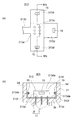
- FIG. 2 is a block diagram showing the configuration of the signal processing system of the camera module 1.
- the camera module 1 has the lens 5 and the image sensor 9 as described above.
- the camera module 1 also includes, for example, a drive unit 31 that drives the imaging device 9, a first processing unit 33 that processes a signal output from the imaging device 9, and a first processing unit that processes a signal output from the first processing unit 33.
- the drive unit 31 generates, for example, a pulse signal for initialization and a pulse signal (drive signal) having a predetermined frequency for signal transfer in the image sensor 9 and inputs the pulse signal to the image sensor 9.
- the image sensor 9 to which the drive signal is input outputs a signal (image data signal) corresponding to the captured image.
- the drive unit 31 outputs a pulse signal to the image sensor 9 so that the image data signal is continuously (repeatedly) output.
- moving image data is obtained from the image sensor 9.
- the first processing unit 33 and the second processing unit 35 perform, for example, a predetermined process on the signal from the image sensor 9 as a whole and output the processed signal to the terminal 7.
- the processing that these processing units perform on the signal from the image sensor 9 includes, for example, amplification processing, A / D conversion processing, filtering processing, AE (Automatic Exposure) processing, AWB (Auto White Balance) processing, and serial conversion processing. , Processing for adding appropriate information such as a header, and / or D / A conversion processing.
- the header includes, for example, information for specifying the order of images of a plurality of frames.
- the first processing unit 33 and the second processing unit 35 perform the above processing by appropriately sharing the processing.
- the first processing unit 33 performs processing on the raw data signal from the image sensor 9.
- the second processing unit 35 performs processing on the signal processed by the first processing unit 33 and outputs the processed signal to the terminal 7. It may be set as appropriate which process is performed by the first processing unit 33.
- the first processing unit 33 and the second processing unit 35 can share the same processing.
- the format of the signal output from the second processing unit 35 to the terminal 7 may be appropriate.
- the signal may be an LVDS (Low (voltage differential signaling) signal.
- the second processing unit 35 may include an electronic component that converts a signal including information to be output into an LVDS signal.
- the signal output from the second processing unit 35 to the terminal 7 is not limited to LVDS, and may be a single-ended signal, for example.
- the control unit 37 controls drive start and drive stop of the drive unit 31, the first processing unit 33, and the second processing unit 35 in accordance with, for example, a control signal input from the terminal 7. Further, for example, the control unit 37 performs a process of supplying clock pulses to these units (31, 33, and 35) and synchronizing them. Note that the division of roles among the drive unit 31, the first processing unit 33, the second processing unit 35, and the control unit 37 may be set as appropriate.
- the input signal to each unit (9, 31, 33, 35 and 37) and the method of the output signal from each unit, the strength of the signal intensity (for example, voltage) and / or the frequency may be appropriately set.
- the frequency of the signal output from the second processing unit 35 described above to the terminal 7 is 500 MHz to 10 GHz, or 1 GHz to 10 GHz.
- the power supply unit 39 converts the power supplied from the terminal 7 into power of an appropriate voltage, current and / or frequency (in the case of alternating current), and supplies the power to each unit (31, 33, 35 and 37).
- the voltage, current, and / or frequency of power supplied from the terminal 7 to the power supply unit 39 may be appropriate.
- the current supplied to the power supply unit 39 is 100 mA to 1 A, or 400 mA to 1 A.
- the hard wafer configurations of the drive unit 31, the first processing unit 33, the second processing unit 35, the control unit 37, and the power supply unit 39 illustrated in FIG. 2 may be appropriate.
- these functional units 31, 33, 35, 37 and 39
- these functional units are constituted by ICs.
- two or more functional units may be configured by one IC, and conversely, one functional unit may be configured by two or more ICs.
- ICs electronic components constituting these functional units (31, 33, 35, 37, and 39) may be mounted on the rigid board 23 (may be included in the assembly 11). It may be mounted on the flexible substrate 13.
- one or more electronic components constituting the drive unit 31, the first processing unit 33, and the control unit 37 are mounted on the rigid board 23.
- one or more electronic components constituting the second processing unit 35 and the power supply unit 39 are mounted on the flexible substrate 13.
- FIG. 2 is only an example. Therefore, for example, among the plurality of functional units (31, 33, 35, 37 and 39), only one or more electronic components constituting the second processing unit 35 are mounted on the flexible substrate 13 or the power supply unit 39. Only one or more electronic components constituting the circuit board are mounted on the flexible substrate 13, or in addition to the second processing unit 35 and the power supply unit 39, one or more electronic components constituting the drive unit 31 and / or the control unit 37 are flexible. It may be mounted on the substrate 13. Further, the power supply unit 39 may be composed of a plurality of electronic components, a part of which is mounted on the flexible substrate 13 and the remaining part is mounted on the rigid substrate 23.
- the electronic component 15 mounted on the flexible substrate 13 as described above is the electronic component 15 described with reference to FIG. Therefore, as can be understood from the above description, the electronic component 15 may be a power supply IC constituting the power supply unit 39, for example. Further, for example, the electronic component 15 may be a component that generates an LVDS-type signal when it constitutes at least a part of the second processing unit 35. As can be understood from the above description, the division of roles for the one or more electronic components 15 to realize the configuration of FIG. 2 may be appropriately set.
- the terminal 7 and the assembly 11 may be indirectly electrically connected via the electronic component 15. That is, in the present embodiment, the flexible substrate 13 does not have to directly electrically connect the terminal 7 and the assembly 11. However, in the description of the present disclosure, for convenience, the flexible substrate 13 may include the terminal 7 and the assembly 11 including indirect electrical connection via the electronic component 15.
- the wiring pattern of the flexible board 13 is designed so that, for example, the above-described signal or power supply current flow is realized and the path is simplified. Therefore, although not particularly illustrated, for example, the wiring pattern between the terminal 7 and the electronic component 15 is located in the terminal connection portion 13a.
- a wiring pattern for connecting the terminal 7 or the electronic component 15 and the assembly 11 extends in order through the terminal connection portion 13a and the relay portion 13b.
- the camera module 1 includes the housing 3, the lens 5, the assembly 11, the terminal 7, and the electronic component 15.
- the housing 3 has a front surface portion 3a, a rear surface portion 3b opposite to the front surface portion 3a, and a side surface portion 3d that connects the front surface portion 3a and the rear surface portion 3b.
- the lens 5 is exposed from the front surface portion 3a.
- the assembly 11 includes the image sensor 9 and is located on the rear surface part 3 b side with respect to the lens 5.
- the terminal 7 is for connection with the outside, which is located on the rear surface portion 3b.
- the flexible substrate 13 includes portions (relay portions 13b and terminal connection portions 13a) extending from the assembly 11 to the terminals 7.
- the electronic component 15 is mounted on the flexible substrate 13.
- the camera module 1 includes a housing 3, a lens 5, an assembly 11, a terminal 7, a connection member (a flexible substrate 13 in the present embodiment), and an electronic component 15. Yes.
- the housing 3 has a front surface portion 3a, a rear surface portion 3b opposite to the front surface portion 3a, and a side surface portion 3d that connects the front surface portion 3a and the rear surface portion 3b.
- the lens 5 is exposed from the front surface portion 3a.
- the assembly 11 includes the image sensor 9 and is located on the rear surface part 3 b side with respect to the lens 5.
- the terminal 7 is for connection with the outside, which is located on the rear surface portion 3b.
- the connecting member (13) is a flexible member that extends from the assembly 11 to the terminal 7.
- the electronic component 15 is electrically connected to the assembly 11 and the terminal 7 and is located in the housing 3 away from the assembly 11 toward the rear surface portion 3b.
- a plurality of electronic components in the housing 3 are dispersed on the flexible substrate 13 and / or on the terminal 7 side of the assembly 11.
- Easy to implement As a result, for example, the possibility that the heat (ie, thermal noise) generated by the plurality of electronic components is concentrated on the assembly 11 is reduced.
- the possibility that heat is transmitted to the image sensor 9 of the assembly 11 is reduced.
- an increase in dark current in the image sensor 9 is suppressed.
- the risk that the luminance will be higher than the actual amount of received light in part or all of the image is reduced. That is, the image quality is improved.
- the flexible substrate 13 that electrically connects the assembly 11 and the terminal 7 is also used for mounting the electronic component 15, for example, the risk of an increase in the number of components is reduced.
- the flexible substrate 13 has a rear surface facing portion 13c facing the inner surface of the rear surface portion 3b.
- the electronic component 15 is mounted in the back surface opposing part 13c.
- the electronic component 15 is mounted in a region of the flexible substrate 13 that is farthest from the assembly 11 toward the terminal 7.
- the effect of reducing the possibility that the heat of the electronic component 15 is transmitted to the image sensor 9 is improved.
- the rear surface facing portion 13 c easily transmits heat to the rear surface portion 3 b, and as a result, easily radiates heat to the outside of the housing 3. Therefore, also from this viewpoint, the effect of reducing the possibility that the heat of the electronic component 15 is transmitted to the image sensor 9 is improved.
- the electronic component 15 may constitute at least one of the power supply unit 39 that supplies power to the image sensor 9 and the second processing unit 35 that processes a signal from the image sensor 9.
- the effect of dispersion of electronic parts is further improved.
- it is as follows.
- the power supply unit 39 converts the supplied power into power of appropriate voltage and / or current and distributes the power to each unit, a relatively large current flows into the power supply unit 39, and a relatively small current flows into the power supply unit 39. To each part. Therefore, when the power supply unit 39 is provided in the assembly 11, a relatively large current flows from the terminal 7 to the assembly 11. On the other hand, when the power supply unit 39 is provided on the flexible substrate 13, a relatively large current flows from the terminal 7 to the middle of the flexible substrate 13, and a relatively small current flows from the middle to the assembly 11. That is, a path through which a relatively large current flows is shortened.
- the amount of heat generated by the supply of power is reduced, and as a result, the amount of heat transmitted to the image sensor 9 is reduced. Therefore, not only the amount of heat transmitted to the image sensor 9 when the power supply unit 39 as a heat source is separated from the image sensor 9 but also the amount of heat transmitted to the image sensor 9 is reduced by the heat amount reduction in the flexible substrate 13. Become. In addition, for example, the current easily falls below the allowable current of the flexible substrate 13, and the degree of freedom in design is improved.
- the power supply unit 39 is provided on the flexible substrate 13
- the power supply unit 39 is separated from the imaging device 9 and its immediate function unit (for example, the first processing unit 33) included in the assembly 11.
- the possibility that radiation noise and conduction noise caused by high-frequency signals such as signals including image information affect the current from the power supply unit 39 is reduced.
- the signal transmission path from the second processing unit 35 to the terminal 7 can be shortened.
- the mutual influence between the signal output from the second processing unit 35 and another signal or current can be reduced.
- the transmission path is shortened, the influence of the transmission path on impedance matching is reduced.
- impedance matching is facilitated. This effect is effective when the second processing unit 35 generates and outputs a signal for transmission, such as an LVDS signal, which is likely to have a high frequency.
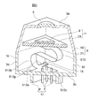
- FIG. 3 is a schematic perspective view showing the camera module 201 according to the second embodiment in a cutaway manner.
- the camera module 201 is mainly different from the camera module 1 of the first embodiment in the shape of the flexible substrate and the mounting position of the electronic component 15. Specifically, it is as follows.
- the flexible board 213 of the camera module 201 has a terminal connection part 213a and a relay part 213b, like the flexible board 13 of the first embodiment. Furthermore, the flexible substrate 213 has an extended portion 213d extending from the terminal connection portion 213a. As described above, the flexible substrate 13 of the first embodiment may be regarded as having the extension 13d.
- the extension portion 213d of the present embodiment has a length that extends from the terminal connection portion 213a and reaches the side surface portion 3d.
- the extension portion 213d has an overlapping region 213da that can overlap the inner surface of the side surface portion 3d.
- the extension portion 213d extends, for example, roughly from the terminal connection portion 213a along the inner surface of the rear surface portion 3b, then bends to the assembly 11 side, and extends along the inner surface of the side surface portion 3d. Therefore, from another viewpoint, the extension portion 213d has a bent portion 213e that bends in the direction of bending the surface thereof, and also has a side surface facing portion 213f that faces the inner surface of the side surface portion 3d.
- the portion of the extended portion 213d that faces the rear surface portion 3b constitutes a rear surface facing portion 213c that faces the inner surface of the rear surface portion 3b of the flexible substrate 213 together with the terminal connection portion 213a or alone.
- the extended portion 213d may be housed in the housing 3 in a manner different from the illustrated example, such as the whole being gently curved with the inner side of the housing 3 being concave.
- the extension portion 213d is generally along the inner surface of the housing 3 as in the illustrated example (the same applies to a third embodiment described later). Accordingly, in the following description, the overlapping region 213da and the side facing portion 213f are generally synonymous.
- the aspect related to the presence or absence of contact with the inner surface of the rear surface portion 3b of the extension portion 213d facing the rear surface portion 3b may be the same as that of the terminal connection portion 13a, as described in the first embodiment.
- the aspect related to the presence or absence of contact with the inner surface of the side surface part 3d of the side facing part 213f is the same as the aspect related to the presence or absence of contact with the inner surface of the rear surface part 3b facing the rear surface part 3b. May be.
- the side facing portion 213f may be bonded to the inner surface of the side surface portion 3d by an adhesive or the like (adhesive layer), or may not be bonded.
- the side facing portion 213f may be in close contact with the inner surface of the side surface portion 3d directly or indirectly via an appropriate material (for example, an adhesive or grease), or separated from the inner surface of the side surface portion 3d through a gap. May be.
- adheres is 80% or more of the area of duplication area
- the extension portion 213d When the extension portion 213d is not bonded to the inner surface of the housing 3 (for example, the overlapping region 213da is not bonded to the inner surface of the side surface portion 3d), the extension portion 213d has a large displacement inward of the housing 3 and / or Alternatively, the movement by a minute force may or may not be restricted. In addition, when it is regulated, for example, the risk of an unintended short circuit is reduced.
- a method of using the restoring force can be used. Since the terminal connection portion 213a is fixed to the housing 3 at least at the position of the terminal 7, the restoring force acts as a force pressing the overlapping region 213da against the side surface portion 3d. Further, for example, a member (not shown) that presses the overlapping region 213da against the side surface portion 3d may be provided.
- the shape and size of the extension 213d may be set as appropriate.
- the extension portion 213d is substantially rectangular with a constant width and extending in a straight line in a direction orthogonal to one side of the terminal connection portion 213a and the side surface portion 3d.
- the width of the extension portion 213d is narrower than the width of the terminal connection portion 213a (the length of one side to which the extension portion 213d is connected). From another viewpoint, the width of the extension portion 213d is smaller than the width of the inner surface of the side surface portion 3d (the length of one side viewed in the optical axis direction).
- extension portion 213d may have a shape other than a rectangle, and the width of the extension portion 213d may be equal to or greater than the width of the terminal connection portion 213a, or substantially equal to the width of the inner surface of the side surface portion 3d. It may be equivalent (for example, 80% or more).
- the overlapping region 213da (the tip) is located relatively far from the assembly 11 in the inner surface of the side surface portion 3d.
- the overlapping region 213da is located closer to the rear surface portion 3b than the intermediate position between the assembly 11 and the inner surface of the rear surface portion 3b.
- the overlapping region 213da may extend to the assembly 11 side from the intermediate position.
- the overlapping region 213da is a large portion of the inner surface of the side surface portion 3d that is closer to the rear surface portion 3b than the assembly 11. It may have an area corresponding to (for example, 80% or more).
- the bent portion 213e is bent, for example, by approximately 90 °.
- the curvature (the length from the rear surface portion 3b to the side surface portion 3d of the bent portion 213e from another viewpoint) may be appropriately set.
- the planar inner surface of the rear surface portion 3b and the planar inner surface of the side surface portion 3d intersect to form a corner portion.
- the corner portion may be chamfered with a flat surface or a curved surface. Good. In this case, the bent portion 213e is likely to come into contact with the inner surface of the housing 3.
- the extension portion 213d has a portion facing the inner surface of the rear surface portion 3b and a portion facing the inner surface of the side surface portion 3d, and the bending portion 213e is a portion between them. The whole or most of the portion 213d may be curved to form the bent portion 213e.
- the bent portion 213e may be bonded to the inner surface of the housing 3, or may not be bonded, or directly or an appropriate material (for example, adhesive or grease). It may be in intimate contact with the inner surface of the housing 3 via a gap, or may not be in close contact. Further, the movement of the bending portion 213e to the inside of the housing 3 may be restricted by the restoring force of the flexible substrate 13 or an appropriate member.
- the electronic component 15 is mounted in the overlapping area 213da.
- the close contact region may include a region where the electronic component 15 is mounted.
- the electronic component 15 is located on the distal end side of the extension portion 213d (the side opposite to the terminal connection portion 213a side) with respect to the bending portion 213e.
- the wiring pattern of the flexible board is naturally different from that in the first embodiment.
- the wiring pattern may be designed so that the configuration of the signal processing system of FIG. 2 is realized and the path is simplified.
- the wiring pattern that connects the terminal 7 and the electronic component 15 extends in order through the terminal connection portion 213a and the extension portion 213d.
- the wiring pattern that connects the electronic component 15 and the assembly 11 extends in order through the extension portion 213d, the terminal connection portion 213a, and the relay portion 213b.
- the electronic component 15 is mounted on the flexible substrate 213 including the portions (the relay portion 213b and the terminal connection portion 213a) extending from the assembly 11 to the terminal 7. From another viewpoint, the electronic component 15 is located in the housing 3 away from the assembly 11 toward the rear surface portion 3b. Therefore, the same effect as the first embodiment is achieved. For example, due to the dispersion of electronic components, thermal noise in the image sensor 9 is reduced and image quality is improved.
- the flexible substrate 213 includes a terminal connection part 213a, a relay part 213b, and an extension part 213d.
- the terminal connection part 213a is connected to the terminal 7 while facing the inner surface of the rear surface part 3b.
- the relay portion 213b extends from a part of the outer edge of the terminal connection portion 213a to the assembly 11.
- the extension part 213d extends from the other part of the outer edge of the terminal connection part 213a.
- the electronic component 15 is mounted on the extension 213d.
- the electronic component 15 can be mounted at a position away from both the assembly 11 and the terminal 7.
- the heat source can be further dispersed.
- the extension portion 213d is provided on the flexible substrate 213, the area where the electronic component 15 can be mounted increases. Therefore, for example, it is easy to increase the number of electronic components 15 mounted on the flexible substrate 213. As a result, it is also easy to meet the demand for multifunctional camera module 201.
- the extension portion 213d has an overlapping region 213da that can overlap the inner surface of the side surface portion 3d.
- the electronic component 15 is mounted in the overlapping area 213da.
- the flexible substrate 213 has a side facing portion 213f facing the inner surface of the side portion 3d.
- the electronic component 15 is mounted on the side facing portion 213f.
- the electronic components can be dispersed not only on the inner surface of the rear surface portion 3b but also on the inner surface of the side surface portion 3d.
- the electronic components can be dispersed not only on the inner surface of the rear surface portion 3b but also on the inner surface of the side surface portion 3d.
- the region where the electronic component 15 can be mounted also extends to the inner surface of the side surface portion 3d, it becomes easy to meet the demand for higher functionality for the camera module 201.
- the output is output from the second processing unit 35.
- High-frequency signals for example, LVDS signals
- LVDS signals are easily separated from the power supply current.
- the mutual influence between the two is reduced.
- a plurality of electronic components can be dispersed even when a space in which the electronic component 15 can be mounted cannot be secured on the inner surface of the rear surface portion 3b.
- the extended portion 213d (extending portion) has a bent portion 213e that is bent in the direction of bending the surface of the flexible substrate 213 on the base side (terminal connecting portion 213a side) from the electronic component 15. is doing.
- the possibility that vibration transmitted from the outside to the terminal 7 is transmitted to the electronic component 15 is reduced.
- the vibration of the terminal connection portion 213a is absorbed by the bending portion 213e.
- the space in the housing 3 in which the terminal 7 and the electronic component 15 are accommodated remains small, and the distance of the flexible substrate 213 between the terminal 7 and the electronic component 15 is ensured. From the viewpoint, vibrations are not easily transmitted.
- the risk of vibration being transmitted to the electronic component 15 for example, the risk of peeling of the electronic component 15 is reduced. Such an effect is effective, for example, when the camera module 201 is for vehicle use.
- FIG. 4A is a development view illustrating a part of the flexible substrate 313 included in the camera module 301 according to the third embodiment.
- FIG. 4B is a cross-sectional view showing a part of the camera module 301 and corresponds to the line IVb-IVb in FIG.
- the camera module 301 is mainly different from the camera module 1 of the second embodiment in the shape of a flexible substrate. Specifically, it is as follows.
- the flexible substrate 313 includes a terminal connection part 313a and a relay part 313b, as in the first and second embodiments.
- the flexible substrate 313 has an extension portion 313d including an overlapping region 313da (side facing portion 313f), as in the second embodiment.
- a plurality of extension portions 313d are provided.
- the plurality of extension portions 313d extend from the terminal connection portion 313a toward a plurality of different side surface portions 3d, and the plurality of overlapping regions 313da can overlap with the different side surface portions 3d. More specifically, for example, of the four side surface portions 3d, the extension portion 313d is provided for the three side surface portions 3d. The remaining one side surface portion 3d is a side surface portion 3d on the side from which the relay portion 313b extends. Therefore, the total number of relay portions 313b and extension portions 313d is the same as the number of side surface portions 3d.
- the number of the plurality of extension portions 313d is not limited to one less than the number of the side surface portions 3d.
- neither the relay portion 313b nor the extension portion 313d extends with respect to any of the plurality of side surface portions 3d, and the number of the plurality of extension portions 313d may be two or more less than the number of the side surface portions 3d.
- the number of the plurality of extending portions 313d may be one less than the number of the side surface portions 3d. It may be a different number (for example, a number less than 2).
- one extended portion 313d may be opposed across two sides (two side surface portions 3d) intersecting at an obtuse angle when viewed in the optical axis direction.
- each extension 313d itself, and the arrangement position of the electronic component 15 in each extension 313d may be the same as those of the extension 213d of the second embodiment.
- the width of the extension is different between FIG. 3 and FIG. 4A, as described in the description of the second embodiment, the width may be appropriately set.
- the division of roles of the plurality of electronic components 15 for realizing the configuration of the signal processing system of FIG. 2 may be appropriately set. The same applies to the plurality of electronic components 15 formed.
- the housing 3 includes the plurality of side surface portions 3d along the outer edges of the front surface portion 3a and the rear surface portion 3b.
- the flexible substrate 313 has a plurality of extension portions 313d extending from the terminal connection portion 313a toward different side surface portions 3d.
- One of the plurality of electronic components 15 is mounted in the overlapping region 313da of each of the plurality of extension portions 313d.
- the effect described in the second embodiment is improved.
- the electronic component is dispersed not only on the inner surface of the rear surface portion 3b but also on the inner surface of the side surface portion 3d, and the effect that heat of the electronic component 15 is radiated from the side surface portion 3d is improved.
- the flexible substrate 313 when the flexible substrate 313 generates a restoring force to return to a flat shape, the plurality of extension portions 313d abut against the side surface portions 3d in different directions and receive a force against the restoring force.
- the flexible substrate 313 is easily held in the rear housing 21 with the terminal connection portion 313a facing the rear surface portion 3b. .
- casing 21 is facilitated.
- the above effect is improved when the total number of relay portions 313b and extension portions 313d is the same as the number of side surface portions 3d. Further, the effect of the position holding by the restoring force is improved when at least two extending portions 313d extend in opposite directions.
- FIG. 5 is a schematic perspective view showing the camera module 401 according to the fourth embodiment in a cutaway view.
- the camera module 401 is mainly different from the camera module 1 of the first embodiment in the shape of a flexible substrate. Specifically, it is as follows.
- the flexible substrate 413 of the camera module 401 has a terminal connection portion 413a and a relay portion 413b, like the flexible substrate 13 of the first embodiment. Furthermore, the flexible substrate 413 has an extension part 413d extending from the terminal connection part 413a.
- the extension portion 413d of the present embodiment is bent, for example, in order from the terminal connection portion 413a side to the assembly 11 side, bent to the opposite side (generally folded back), and further bent to the opposite side. That is, the extended portion 413d has bent portions 413e that are alternately bent three times in the direction in which the surface of the flexible substrate 413 is bent.
- the electronic component 15 is mounted on a portion of the extension portion 413d on the tip side (the side opposite to the terminal connection portion 413a) from the bent portion 413e.
- the tip side portion of the bent portion 413e faces the inner surface of the rear surface portion 3b.
- This front end portion constitutes a rear surface facing portion 413c that faces the inner surface of the rear surface portion 3b together with the terminal connecting portion 413a or alone.
- the bent portion 413e is not fixed, bonded, or in close contact with the housing 3 (rear surface portion 3b), for example, and is in a floating state.
- the portion on the tip side of the bent portion 413e the presence or absence of adhesion and / or adhesion and the mode thereof may be set as appropriate, similarly to the rear surface facing portion of the other embodiments.
- the base part of the extension part 413d (a part or all of the bent part 413e) is formed by cutting out one side of the rectangle of the terminal connection part 413a. Even if one side of the rectangle is cut out in this way, the extension portion 413d may be regarded as extending from the outer edge of the terminal connection portion 413a (the shape in which one side of the rectangle is cut out is connected to the terminal). This may be regarded as the shape of the portion 413a.)
- the curvature and length of the bent portion 413e may be set as appropriate.
- the width of the extension portion 413d (bending portion 413e) is shorter than the length of one side of the terminal connection portion 413a to which the extension portion 413d is connected, as in FIG.
- the extension portion 413d (bending portion 413e) may have a width equivalent to the length of one side of the terminal connection portion 413a, as in FIG.
- the extended portion 413d (extending portion) has the bent portion 413e that is bent in the direction of bending the surface of the flexible substrate 413 on the root side of the electronic component 15.
- the bent portions 413e are alternately bent twice or more in the direction in which the surface of the flexible substrate 413 is bent.
- the effect of the bent portion 213e described in the description of the second embodiment is improved.
- the effect of reducing the possibility that the vibration of the terminal 7 is transmitted to the electronic component 15 is improved.
- the bent portions 413e that are alternately bent two or more times not only bend, but also can be expanded and contracted, and vibrations can be absorbed by the expansion and contraction. Therefore, the vibration reduction effect is greatly improved.
- the bent portion 413e is bent twice or more, it is three-dimensionally arranged in the housing 3, so that the internal space of the housing 3 can be effectively used.
- FIG. 6 is a schematic perspective view showing the camera module 501 according to the fifth embodiment in a cutaway manner.
- the camera module 501 is mainly different from the camera module 1 of the first embodiment in the shape of the flexible substrate. Specifically, it is as follows.
- the flexible substrate 513 of the camera module 501 has a terminal connection portion 513a and a relay portion 513b, as with the flexible substrate 13 of the first embodiment. Furthermore, the flexible substrate 513 has a branching part 513g extending so as to branch from the relay part 513b to the terminal connection part 513a. And the electronic component 15 is mounted in the branch part 513g.
- the position, shape and size of the branch part 513g may be set as appropriate.
- the branching portion 513g extends from the portion on the terminal connection portion 513a side of the relay portion 513b in a direction substantially orthogonal to the relay portion 513b (in another direction, toward the one side surface portion 3d). . Thereafter, the branching portion 513g extends substantially along the inner surface of the rear surface portion 3b. The tip does not reach the side surface portion 3d.
- the branching portion 513g may have a portion that reaches the side surface portion 3d and faces the side surface portion 3d (a portion corresponding to the overlapping region 213da in the second embodiment).
- the shape of the branch portion 513g is, for example, generally rectangular.
- the branching part 513g (at least a part on the front end side in the illustrated example) faces the inner surface of the rear surface part 3b.
- the electronic component 15 is mounted on, for example, a portion facing the inner surface of the rear surface portion 3b.
- the electronic component 15 may be mounted on a portion of the branching portion 513g that does not face the rear surface portion 3b.
- the electronic component 15 is mounted on the portion. It may be done.
- the portion of the branching portion 513g that faces the rear surface portion 3b constitutes a rear surface facing portion 513c that faces the inner surface of the rear surface portion 3b of the flexible substrate 513 together or alone with the terminal connection portion 513a.
- the portion facing the rear surface portion 3b of the branching portion 513g the presence or absence of adhesion and / or adhesion and the mode thereof may be appropriately set as in the rear surface facing portion of the other embodiments.
- the branching portion 513g has a side facing portion that faces the inner surface of the side portion 3d.
- the branch part 513g extends from the relay part 513b instead of from the terminal connection part 213a.
- the wiring pattern of the flexible board is different from that of the other embodiments. Is different.
- the wiring pattern may be designed so that the configuration of the signal processing system of FIG. 2 is realized and the path is simplified.
- the wiring pattern that connects the terminal 7 and the electronic component 15 extends in order through the terminal connection portion 513a, a part of the relay portion 513b on the terminal connection portion 213a side, and the branch portion 513g.
- the wiring pattern that connects the electronic component 15 and the assembly 11 extends partly on the assembly 11 side of the branch part 513g and the relay part 513b.
- the flexible substrate 513 includes the branch portion 513g extending so as to branch from the relay portion 513b to the terminal connection portion 513a.
- the electronic component 15 is mounted on the branch portion 513g.
- the relay portion 513b generates vibration from the terminal connection portion 213a to the electronic component 15. It can function as a damping buffer. As a result, for example, peeling of the electronic component 15 is suppressed.
- the extension portion 213d is connected to the terminal connection portion 213a without passing through the relay portion 513b, so that the route between the terminal 7 and the electronic component 15 is shortened. Heat generation and / or noise superposition can be suppressed.
- FIG. 7 is a schematic perspective view showing the camera module 601 according to the sixth embodiment in a cutaway manner.
- the camera module 601 is mainly different from the camera module 1 of the first embodiment in the shape of a flexible substrate. Specifically, it is as follows.
- the flexible substrate 613 of the camera module 601 includes a terminal connection portion 613a, a relay portion 613b, and a branching portion 613g, similarly to the flexible substrate 513 of the fifth embodiment.
- the branch part 613g has a bent part 613e.
- An electronic component 15 is mounted on a portion of the branch portion 613g that is closer to the tip than the bent portion 613e (the side opposite to the relay portion 613b).
- the bent portion 613e is a portion bent in a plan view when the flexible substrate 613 is developed.
- the overall shape and various dimensions of the branch portion 613g including the bent portion 613e and the position in the housing 3 may be set as appropriate.
- the branch part 613g extends in a direction substantially orthogonal to the relay part 613b from the relay part 613b (in a direction from the other side part to the side part 3d), similarly to the branch part 513g of the fifth embodiment. . Thereafter, the branch portion 613g is bent at an angle of approximately 90 ° before reaching the inner surface of the extended side surface portion 3d when viewed in the optical axis direction, and extends along the inner surface of the side surface portion 3d. . That is, the shape of the branch part 613g is roughly L-shaped. The two straight portions constituting the L shape are, for example, rectangular.
- the branching portion 613g (extending portion) can be regarded as extending along the shape of the inner surface of the outer peripheral surface portion 3c when viewed in the optical axis direction. Further, from another viewpoint, it can be understood that the branch portion 613g extends along the outer edge of the terminal connection portion 613a when viewed in the optical axis direction.
- the angle at which the bent portion 613e bends is formed by the two side surface portions 3d (or two sides of the terminal connection portion 613a). It can be understood that the angle is the same as the angle.
- the branching portion 613g may not be along the inner surface of the outer peripheral surface portion 3c and / or the outer edge of the terminal connection portion 613a when viewed in the optical axis direction.
- the angle of the bent portion 613e may be an angle other than 90 °.
- the bent portion 613e may be curved instead of bent. In the case of bending, the outer edge may be chamfered appropriately.
- the branch portion 613g may or may not have the same width before and after the bent portion 613e.
- the length of the branch part 613g may be set as appropriate.
- the branch part 613g is at least partially opposed to the inner surface of the rear surface part 3b, for example, like the branch part 513g of the fifth embodiment.
- most of the branching portion 613g, including the tip faces the inner surface of the rear surface portion 3b.
- the portion where the electronic component 15 on the tip side of the bent portion 613e is mounted also faces the inner surface of the rear surface portion 3b, for example.
- a portion of the branching portion 613g that faces the rear surface portion 3b constitutes a rear surface facing portion 613c that faces the inner surface of the rear surface portion 3b of the flexible substrate 613 together with the terminal connection portion 613a or alone.
- the presence or absence of adhesion and / or adhesion and the mode thereof may be appropriately set as in the rear surface facing portion of the other embodiments.
- the electronic component 15 is mounted on the branching portion 613g (extending portion).
- the branch portion 613g has a bent portion 613e that is bent in a plan view when the flexible substrate 613 is deployed on the base side (relay portion 613b side) from the electronic component 15.
- the possibility that vibration transmitted from the outside to the terminal 7 is transmitted to the electronic component 15 is reduced.
- vibration is easily absorbed by the bent portion 613e.
- the space in the housing 3 in which the terminal 7 and the electronic component 15 are accommodated is kept small, and the distance of the flexible substrate 613 between the terminal 7 and the electronic component 15 is ensured. From the viewpoint, vibrations are not easily transmitted.
- the risk of vibration being transmitted to the electronic component 15 for example, the risk of peeling of the electronic component 15 is reduced.
- FIG. 8 is a schematic perspective view showing the camera module 701 according to the seventh embodiment in a cutaway manner.
- the camera module 701 is mainly different from the camera module 1 of the first embodiment in the shape of a flexible substrate. Specifically, it is as follows.
- the flexible substrate 713 of the camera module 701 has a terminal connection portion 713a, a relay portion 713b, and a branching portion 713g, like the flexible substrate 513 of the fifth embodiment.
- the branch part 713g has a bent part 713e like the branch part 613g of the sixth embodiment, and the electronic component 15 is mounted on the tip side of the bent part 713e of the branch part 713g.
- the branching portion 713g extends so that the surface is along the inner surface of the outer peripheral surface portion 3c.
- the branch portion 713g extends from a portion of the relay portion 713b that is slightly away from the terminal connection portion 713a.
- the portion from which the branch portion 713g of the relay portion 713b extends is, for example, the portion of the relay portion 713b that is closest to the inner surface of the outer peripheral surface portion 3c.
- the surface may be brought into contact with the inner surface of the outer peripheral surface portion 3c by a restoring force for returning to the flat shape of the relay portion 713b.
- the branch portion 713g extends along the first side surface portion 3d close to the relay portion 713b, and further extends along the second side surface portion 3d intersecting the first side surface portion 3d. .
- the portion of the branching portion 713g that transitions from the first side surface portion 3d to the second side surface portion 3d bends in the direction of bending the surface of the flexible substrate 713, similarly to the bending portion 213e of the second embodiment (FIG. 3).
- a bent portion 713e is formed.
- the overall shape of the branching portion 713g, various dimensions, and the position in the housing 3 may be set as appropriate.
- the branching portion 713g has an elongated shape extending approximately linearly with a constant width.
- the branch portion 713g (electronic component 15) is located closer to the rear surface portion 3b than the intermediate position between the assembly 11 and the inner surface of the rear surface portion 3b.
- a part or all of the branching portion 713g may be located closer to the assembly 11 than the intermediate position.
- the length of the branch part 713g may also be set as appropriate.
- At least a part of the branching part 713g (for example, a region where the electronic component 15 is mounted) constitutes a side facing part 713f that faces the side part 3d, for example. Whether or not the side facing portion 713f is adhered to and / or adhered to the side surface portion 3d and the mode thereof may be appropriately set similarly to the side facing portion 213f of the second embodiment (FIG. 3).
- the electronic component 15 is mounted on the flexible substrate 713 including the portions (the relay portion 713b and the terminal connection portion 713a) extending from the assembly 11 to the terminal 7. From another viewpoint, the electronic component 15 is located in the housing 3 away from the assembly 11 toward the rear surface portion 3b. Accordingly, various effects similar to those of the other embodiments are exhibited. For example, due to the dispersion of electronic components, thermal noise in the image sensor 9 is reduced and image quality is improved.
- the branch portion 713g extending from the relay portion 713b is disposed so as to extend along the inner surface of the side surface portion 3d. Therefore, for example, as compared with the sixth embodiment (FIG. 7), the branching portion 713g has a higher degree of freedom in designing the position in the optical axis direction. In the sixth embodiment, for example, the branch portion 613g can be separated from the assembly 11 as much as possible as compared with the present embodiment.
- the flexible substrate that connects the assembly 11 and the terminal 7 may be a single-sided substrate, a double-sided substrate, or a multilayer substrate.
- the reference potential layer may be provided in a layer different from the layer in which the wiring pattern is provided.
- FIG. 9A to FIG. 9C are diagrams showing an example of the flexible substrate 13 having a reference potential layer.
- FIG. 9A is a partial cross-sectional view of the flexible substrate 13 and corresponds to the line IXa-IXa in FIG. 9B.
- FIG. 9B is a plan view of a part of the flexible substrate 13 on the side where the electronic component 15 is mounted (above the paper surface of FIG. 9A).
- FIG. 9C is a plan view of the side opposite to FIG. 9B (downward in FIG. 9A).
- the thickness of the flexible substrate 13 is shown such that the ratio to the dimension in the plane direction is larger than the actual ratio.
- the outline of the electronic component 15 when the flexible substrate 13 is seen through is also indicated by a dotted line.
- the code of the first embodiment is used for the flexible substrate, but the configuration of this example may be applied to other embodiments.
- the terminal 7 to which the reference potential is applied is denoted by 7G, and the other terminals 7 are denoted by 7A. Is attached.
- the electronic component 15 is taken as an example for easy illustration.
- the electronic component 15 is a chip-type component having a pair of pad-shaped terminals 15a, for example.
- the configuration of the electronic component 15 is not limited to such a configuration, and may have three or more terminals or a lead-shaped terminal. It may be.
- the flexible substrate 13 is, for example, a double-sided substrate. That is, the flexible substrate 13 overlaps the insulating and film-like base material 41, the first conductive layer 43 overlapping one surface (first surface 41a), and the other surface (second surface 41b). Second conductive layer 45. Although not particularly illustrated, as described above, the first conductive layer 43 and the second conductive layer 45 may be appropriately covered with a solder resist or the like.
- the first conductive layer 43 includes a plurality of (here, two) first conductor patterns 43a on which the electronic component 15 is mounted.
- each first conductor pattern 43a includes, for example, a pad-like land on which the electronic component 15 is mounted and a wiring extending from the land.
- the land and the wiring are indicated by a rectangle extending with a certain width, and the boundary between the both is ambiguous.
- the land of the first conductor pattern 43a and the terminal 15a of the electronic component 15 are joined by a bump-like conductive joining material 47 (for example, solder). Thereby, the electronic component 15 is mounted on the flexible substrate 13.
- the wiring of the first conductor pattern 43a is connected to the terminal 7A or another electronic component.
- the other electronic component may be mounted on the flexible substrate 13 or may be mounted on the assembly 11, for example.
- the first conductor pattern 43a on the left side of the drawing is connected to the terminal 7A. More specifically, the hole 13h is formed in the flexible substrate 13 at the position of the wiring of the first conductor pattern 43a, the terminal 7A is inserted into the hole 13h, and the terminal 7A and the wiring are connected by a bonding material (not shown). Are joined. Further, the wiring of the first conductor pattern 43a on the right side of the paper extends to the outside of the illustrated region (above the paper surface of FIG. 7B) and is connected to other electronic components.
- the first conductive layer 43 may include a second conductor pattern 43b connected to a terminal 7G to which a reference potential is applied.
- the second conductor pattern 43b is connected to the terminal 7G in the same manner as the first conductor pattern 43a.
- the second conductor pattern 43b is not connected to the electronic component, but may be connected to the electronic component including wiring and the like, like the first conductor pattern 43a.
- the second conductive layer 45 spreads in a solid shape, for example, over substantially the entire surface of the flexible substrate 13 (for example, 80% or more). Therefore, for example, the second conductive layer 45 includes a portion that extends from the periphery of the terminal 7 to a region overlapping the electronic component 15 in a plan perspective when the flexible substrate 13 is developed. For example, the second conductive layer 45 includes a portion that overlaps the entirety of the electronic component 15 in a plan perspective.
- the second conductive layer 45 is connected to a terminal 7G to which a reference potential is applied.
- the connection mode is the same as the connection mode between the first conductive layer 43 and the terminal 7. Therefore, the second conductive layer 45 extends to the vicinity of the edge of the hole 13h through which the terminal 7G is inserted. On the other hand, the second conductive layer 45 is separated from the hole 13h through which the terminal 7A is inserted.
- the second conductive layer 45 to which the reference potential is applied is provided on the flexible substrate 13 as described above, for example, noise from the outside can be blocked. Further, for example, when this example is applied to the third embodiment (FIGS. 4A and 4B), the second conductive layer 45 is positioned at the rear surface facing portion 313 c and the plurality of side surface facing portions 313 f.
- the part functions like a shield case, and the noise blocking effect is improved. By blocking the noise, for example, the image quality is improved.
- extension parts 213d, 313d and 413d and the branch parts 613g and 713g are examples of the extension part which has a bending part.
- the flexible boards 13, 213, 313, 413, 513, 613, and 713 are examples of flexible connection members that extend from the assembly to the terminals.
- the rear surface facing portion that faces the inner surface of the rear surface portion of the housing and on which the electronic component is mounted may be, for example, a terminal connection portion as in the first embodiment, or the fourth embodiment. It may be an extension part that extends from the terminal connection part as shown in FIG. 5B, or branches from the relay part (part extending from the terminal connection part to the assembly) to the terminal connection part as in the fifth or sixth embodiment. It may be a branch part.
- the side facing portion on the flexible substrate that faces the inner surface of the side surface portion of the housing and on which the electronic component is mounted is, for example, an extended portion that extends from the terminal connection portion as in the second or third embodiment. (The overlapping area among them) may be used, or a branching part branched from the relay part to the terminal connection part as in the seventh embodiment.
- the first to seventh embodiments may be appropriately combined.
- an extension second to fourth embodiments: FIGS. 3 to 5 extending from the terminal connection portion and a branching portion (fifth to seventh embodiments: FIGS. 6 to 8) branching from the relay portion Both may be provided.
- the bending part (fourth embodiment: FIG. 5) that bends the surface of the flexible substrate twice or more in the direction of bending is not only an extension part that fits in the rear surface part, but also an extension part (second and third embodiments: 3 and 4) and the branching portion (fifth to seventh embodiments: FIGS. 6 to 8) may be applied to the side facing portion as well as the rear facing portion.
- the bent part (sixth embodiment: FIG.
- the electronic component is mounted on a flexible board extending from the assembly to the terminal. It is not a requirement. For example, apart from a flexible board (or other flexible connecting member) extending from the assembly to the terminals, a rigid board on which electronic components are mounted is provided on the inner surface of the rear surface portion, or connected to the assembly by electric wires. The electronic component may be directly fixed to the inner surface of the rear surface portion.
- the mounting position of the electronic component is not limited to the terminal connection portion, the extension portion, or the branch portion, and may be a relay portion, for example.
- electronic components may be mounted on these two or more parts.
- the electronic component mounted on the flexible substrate may be located in the vicinity of the assembly. Even in this case, compared with the case where the electronic component is mounted on the rigid board of the assembly, for example, the heat transferred from the electronic component to the imaging device via the conductor is reduced, or the electronic component of the flexible board and Conduction noise between the electronic components of the assembly is reduced.
- each part of the flexible substrate is not limited to those exemplified in the embodiment.
- the relay portion extending from the terminal to the assembly may be shaped to be bent in an L shape when deployed in a planar shape.
- the extension part extended from the terminal connection part and the branch part branched from the relay part may have a three-dimensional shape that cannot be said to face the rear surface part or the side part.
- the assembly is not limited to an assembly in which electronic components are mounted on one rigid board.
- the assembly may be configured by stacking two or more rigid substrates in the optical axis direction.
- the imaging element may be mounted on the most rigid substrate, and a flexible substrate extending from the terminal may be connected to the most rigid substrate.
- the connector for connecting to the outside of the camera module is not limited to the one in which the terminal is directly fixed to the flexible substrate and the housing as in the embodiment.
- the connector may have a connector housing and a plurality of terminals held by the connector housing, be mounted on a flexible substrate, and be exposed from the camera module housing.
- another metal member may be interposed between the terminal and the flexible substrate. Even if the other metal member in the connector is interposed in this way, the flexible substrate may be regarded as extending from the assembly to the terminal and / or connected to the terminal.
Landscapes
- Engineering & Computer Science (AREA)
- Multimedia (AREA)
- Signal Processing (AREA)
- Microelectronics & Electronic Packaging (AREA)
- Physics & Mathematics (AREA)
- Power Engineering (AREA)
- General Physics & Mathematics (AREA)
- Electromagnetism (AREA)
- Condensed Matter Physics & Semiconductors (AREA)
- Computer Hardware Design (AREA)
- Studio Devices (AREA)
- Camera Bodies And Camera Details Or Accessories (AREA)
- Structure Of Printed Boards (AREA)
- Combinations Of Printed Boards (AREA)
Abstract
カメラモジュールは、筐体と、レンズと、アセンブリと、端子と、電子部品とを有している。筐体は、前面部、その反対側の後面部、及び前面部と後面部とをつなぐ側面部を有している。レンズ5は、前面部から露出している。アセンブリは、撮像素子を含んでおり、レンズに対して後面部側に位置している。端子は、後面部に位置している、外部との接続用のものである。フレキシブル基板は、アセンブリから端子へ延びている部分を含んでいる。電子部品は、フレキシブル基板に実装されている。
Description
本開示は、カメラモジュールに関する。
車載用のカメラモジュールのように、システムの要素として利用されるカメラモジュールが知られている(例えば特許文献1)。特許文献1のカメラモジュールは、筐体と、筐体の前面に露出するレンズと、筐体の後面に露出する外部接続用の端子とを有している。筐体の内部には、レンズ側から端子側へ順に、撮像素子、撮像素子が実装されているリジッド式の第1の回路基板、第1の回路基板に接続されているリジッド式の第2の回路基板、第2の回路基板と端子とを接続しているフレキシブル基板が設けられている。第2の回路基板には、回路チップ(電子部品)が実装されている。フレキシブル基板は、第2の基板と端子とを接続する信号線パターン部と、信号線パターン部に対して分岐しているGND線パターン部とを有している。GND線パターン部は、筐体内のシールドケースに接続されている。
本開示の一態様に係るカメラモジュールは、筐体と、レンズと、アセンブリと、端子と、フレキシブル基板と、電子部品と、を有している。前記筐体は、前面部、その反対側の後面部、及び前記前面部と前記後面部とをつなぐ側面部を有している。前記レンズは、前記前面部から露出している。前記アセンブリは、撮像素子を含んでおり、前記レンズに対して前記後面部側に位置している。前記端子は、前記後面部に位置している、外部との接続用のものである。前記フレキシブル基板は、前記アセンブリから前記端子へ延びている部分を含んでいる。前記電子部品は、前記フレキシブル基板に実装されている。
本開示の一態様に係るカメラモジュールは、筐体と、レンズと、アセンブリと、端子と、接続部材と、電子部品と、を有している。前記筐体は、前面部、その反対側の後面部、及び前記前面部と前記後面部とをつなぐ側面部を有している。前記レンズは、前記前面部から露出している。前記アセンブリは、撮像素子を含んでおり、前記レンズに対して前記後面部側に位置している。前記端子は、前記後面部に位置している、外部との接続用のものである。前記接続部材は、前記アセンブリから前記端子まで延びている可撓性のものである。前記電子部品は、前記アセンブリ及び前記端子に電気的に接続されているとともに、前記筐体内で、前記アセンブリから前記後面部側に離れて位置している。
以下、本開示の実施形態について、図面を参照して説明する。なお、以下の説明で用いられる図は模式的なものである。従って、例えば、細部は省略されていることがあり、また、図面上の寸法比率は現実のものとは必ずしも一致していない。
第2実施形態以降において、既に説明された構成と共通または類似する構成について、既に説明された構成に付した符号を用い、また、図示や説明を省略することがある。なお、既に説明された構成と対応(類似)する構成は、既に説明された構成と異なる符号を付した場合においても、特に断りがない点については、既に説明された構成と同様とされてよい。
(第1実施形態)
図1は、第1実施形態に係るカメラモジュール1を破断して示す模式的な斜視図である。
図1は、第1実施形態に係るカメラモジュール1を破断して示す模式的な斜視図である。
カメラモジュール1は、例えば、車載用のものであり、運転支援及び/又は運転の記録等に利用される。例えば、カメラモジュール1は、縦、横及び高さそれぞれの寸法が1cm以上5cm以下の大きさとされており、車体の内部又は外部に、車体の前方、後方又は側方を撮像する向きで設けられる。カメラモジュール1は、不図示のECU(Electronic Control Unit又はEngine Control Unit)に電気的に接続されており、ECUによって制御され、また、カメラモジュール1から出力した信号は、ECUによって処理される。
なお、カメラモジュール1の用途は車載用に限定されないし、その寸法も、上記に例示した寸法よりも小さくてもよいし、大きくてもよい。ただし、以下では、カメラモジュール1が車載用のものである場合を例に取って説明することがある。
(カメラモジュールの全体構成)
カメラモジュール1は、例えば、筐体3と、筐体3から露出しているレンズ5と、筐体3のレンズ5とは反対側に位置している外部接続用の複数の端子7とを有している。レンズ5の位置から理解されるように、カメラモジュール1は、紙面上方側を撮像側としている。また、紙面上下方向は光軸方向である。複数の端子7は、カメラモジュール1が車載用のものである場合においては、不図示のケーブルを介してECUに接続される。
カメラモジュール1は、例えば、筐体3と、筐体3から露出しているレンズ5と、筐体3のレンズ5とは反対側に位置している外部接続用の複数の端子7とを有している。レンズ5の位置から理解されるように、カメラモジュール1は、紙面上方側を撮像側としている。また、紙面上下方向は光軸方向である。複数の端子7は、カメラモジュール1が車載用のものである場合においては、不図示のケーブルを介してECUに接続される。
また、カメラモジュール1は、筐体3の内部に、撮像素子9を含むアセンブリ11と、アセンブリ11から複数の端子7へ延びているフレキシブル基板13と、フレキシブル基板13に実装されている電子部品15とを有している。これらによって、例えば、レンズ5が撮像素子9上に結んだ像が電気信号に変換され、複数の端子7のいずれかから出力される。特に図示しないが、カメラモジュール1は、上記の他、例えば、シールドケースを有していてもよい。
カメラモジュール1から出力される信号は、例えば、撮像した画像を再現するための情報(画像データ)を含む信号である。カメラモジュール1は、例えば、時間経過に伴って得られた複数の画像データ(複数フレームの画像データ)の信号を順次出力することによって、動画像の情報の提供に寄与する。なお、カメラモジュール1は、必要に応じて静止画像を取得する用途に用いられるものであっても構わない。また、カメラモジュール1は、画像データの信号に加えて、又は代えて、画像データに基づく何らかの判定結果の情報を出力してもよい。
(筐体)
筐体3は、例えば、レンズ5を保持する部分(前面部3a、鏡筒)と、アセンブリ11等を収容する部分と、コネクタ17を構成する部分(コネクタ筐体部3f)とを含んでいる。なお、このように、本実施形態の説明では、筐体の語は、純粋な箱状部分だけでなく、比較的広い部分を指している。筐体3の内部は、例えば、基本的に密閉されている。
筐体3は、例えば、レンズ5を保持する部分(前面部3a、鏡筒)と、アセンブリ11等を収容する部分と、コネクタ17を構成する部分(コネクタ筐体部3f)とを含んでいる。なお、このように、本実施形態の説明では、筐体の語は、純粋な箱状部分だけでなく、比較的広い部分を指している。筐体3の内部は、例えば、基本的に密閉されている。
筐体3の外形は、適宜な形状とされてよい。図示の例では、筐体3の外形は、概略、底面が正方形の直角柱(端子7側)と、底面が正方形の錐台(レンズ5側)との組み合わせの形状となっている。別の観点では、筐体3は、光軸方向に見て、概略矩形の外形を有している。図1は、その矩形の一の対角線に沿って破断した模式的な斜視図となっている。また、コネクタ筐体部3fは、複数の端子7を囲むように突出する筒状に形成されている。ここでいう筒は、接続方向(ここでは光軸方向と同じ方向)に見て、円形であってもよいし、矩形であってもよい。
もちろん、筐体3の外形は、上記の形状に限定されるものではない。例えば、筐体3の外形の概略形状は、直方体であってもよいし、直方体(端子7側)と当該直方体から突出する円柱(レンズ5側)との組み合わせの形状であってもよいし、四角形以外の多角形(例えば5角形)を底面とする直角柱であってもよいし、そのような直角柱(端子7側)と当該直角柱から突出する円柱(レンズ5側)との組み合わせであってもよいし、円柱であってもよいし、よりデザイン性が高い形状であってもよい。上記で挙げた各円柱は、レンズ5を保持する鏡筒とされている部分であってよい。なお、以下では、図示の例のように、筐体3の外形が端子7側に直方体状又は直角柱状の部分を含む場合を例に取って説明することがある。
筐体3の内部空間の形状(内表面の形状)も適宜な形状とされてよい。図示の例では、筐体3の内部空間の形状は、概略、上述した筐体3の外形と相似形となっている。従って、筐体3は、少なくとも端子7側に概略直方体状の空間を有している。別の観点では、筐体3は、端子7側に、光軸に直交する平面状の内面(後面部3bの内面)と、その四方を囲む平面状の壁面(側面部3dの内面)を有している。
もちろん、筐体3の内部空間の形状は、上記の形状に限定されるものではなく、例えば、端子7側に、四角柱以外の多角柱又は円柱を含む形状であってもよい。ただし、以下の説明では、端子7側に概略直方体状の空間が形成されている場合を例に取って説明することがある。
筐体3を複数の部位に分けて考えると、例えば、筐体3は、撮像側(レンズ5の前側)に面する前面部3aと、その反対側の後面部3bと、前面部3aと後面部3bとをつなぐ外周面部3c(側面部3d)とを有している。外周面部3cは、前面部3aと後面部3bとをその全周に亘ってつなぐ部分である。外周面部3cのうち、光軸方向に見て多角形の辺となる部分については、側面部3dというものとする。図示の例では、外周面部3cは、筐体3の外形が少なくとも端子7側に直角柱状の部分を含んでいることから、4つの側面部3dを有している。
上述した筐体3の外形の説明から理解されるように、これら各部(3a~3d)の外表面の形状は、適宜な形状とされてよい。図示の例では、前面部3aの外表面は錐台の上底を構成している。後面部3bの外表面は、直角柱の底面(端子7側)を構成している。外周面部3c(側面部3d)の外表面は、錐台の側面及び直角柱の側面を構成している。
なお、筐体3の外形に応じて、各部(3a~3d)の境界は適宜に定義されてよい。例えば、図示の例とは異なり、筐体3の外形が直方体(端子7側)と直方体から突出する円柱(レンズ5側)との組み合わせの形状である場合、前面部3aは、円柱のレンズ5側の底面を構成する部分と定義されてもよいし、円柱全体と直方体の円柱側の平面とを構成する部分と定義されてもよい。
各部(3a~3d)の形状は、上述した筐体3の外表面及び内表面の形状を実現するように適宜に設定されてよい。図示の例では、前面部3a、後面部3b及び外周面部3cそれぞれは、概略、これらの外表面が面する方向を厚さ方向とする概ね一定の厚さの板状に形成されている。なお、ここでいう板状は、平板状(図示の例)だけでなく、湾曲した板状(例えば円筒を構成するような板状)のものを含む。
もちろん、各部(3a~3d)の形状は、上記のような各部の外表面が面する方向を厚さ方向とする板状に限定されない。例えば、筐体3は、光軸周りの筒状部分(レンズ5を保持する鏡筒)を含み、前面部3aは、その筒状部分の先端部(筒の縁部)であってもよい。
筐体3は、例えば、複数の部材が組み合わされて構成されている。筐体3の分割位置(複数の部材間の境界の位置)、及び複数の部材の数等は適宜に設定されてよい。例えば、筐体3は、レンズ5側の前側筐体19と、その反対側の後側筐体21とを有している。
前側筐体19は、レンズ5とは反対側が開放された箱状(箱は直方体状に限定されない。以下、同様。)の部材である。後側筐体21は、レンズ5側が開放された箱状の部材である。そして、両者の開放側同士を連結することによって、筐体3が構成されている。両者の連結は、係合、ねじ止め、接着など、公知の種々の方法によってなされてよい。また、一方の開放側縁部は、他方の開放側縁部の内側に嵌合してもよい。
特に図示しないが、前側筐体19及び後側筐体21それぞれは、更に複数の部材によって構成されていてよい。例えば、前側筐体19は、レンズ5を保持する鏡筒と、少なくとも外周面部3cのレンズ5側部分を構成する部材とが互いに固定されて構成されていてもよい。この固定は、筐体3内の他の部材を介して間接的になされていてもよい。また、例えば、後側筐体21は、後側筐体21のコネクタ筐体部3f以外の部分を構成する部材と、コネクタ筐体部3fを構成する部材とが互いに固定されて構成されていてもよい。
筐体3の材料は、例えば、基本的に絶縁性材料とされている。絶縁性材料は、例えば、樹脂である。なお、セラミック等の他の絶縁性材料が用いられてもよい。また、筐体3は、一部又は全部に導体(金属)が用いられていてもよい。例えば、筐体3は、樹脂に金属(シールドケース)が埋設されたものであってもよいし、基本的に樹脂からなり、内面の適宜な位置に導電性の塗料が塗布されたものであってもよい。
(レンズ)
レンズ5は、単一のレンズからなる単レンズであってもよいし、複数のレンズからなるレンズ群(光学系)であってもよい。レンズ5は、前面部3aに形成された開口内に配置されて筐体3の外部に露出している。そして、レンズ5は、筐体3の外部からの光を集光して筐体3の内部(撮像素子9上)に像を結ぶ。なお、レンズ5が前面部3aから露出しているという場合、レンズ5が前面部3a側から視認可能であることをいい、外気に触れていることは必ずしも必要ない。従って、例えば、レンズ5は、筐体3の一部を構成する透明カバーによって覆われていてもよい。なお、当該透明カバーをレンズ5の一部と捉えることも可能である。
レンズ5は、単一のレンズからなる単レンズであってもよいし、複数のレンズからなるレンズ群(光学系)であってもよい。レンズ5は、前面部3aに形成された開口内に配置されて筐体3の外部に露出している。そして、レンズ5は、筐体3の外部からの光を集光して筐体3の内部(撮像素子9上)に像を結ぶ。なお、レンズ5が前面部3aから露出しているという場合、レンズ5が前面部3a側から視認可能であることをいい、外気に触れていることは必ずしも必要ない。従って、例えば、レンズ5は、筐体3の一部を構成する透明カバーによって覆われていてもよい。なお、当該透明カバーをレンズ5の一部と捉えることも可能である。
(端子)
端子7は、例えば、ピン状の金属によって構成されている。各端子7は、例えば、後面部3bに形成された孔に挿通されており、はんだ等の接合材によって後面部3bに対して固定されている。また、複数の端子7は、例えば、フレキシブル基板13に形成された孔に挿通されており、はんだ等の導電性の接合材によってフレキシブル基板13の配線(導電パターン)に対して接合されている。
端子7は、例えば、ピン状の金属によって構成されている。各端子7は、例えば、後面部3bに形成された孔に挿通されており、はんだ等の接合材によって後面部3bに対して固定されている。また、複数の端子7は、例えば、フレキシブル基板13に形成された孔に挿通されており、はんだ等の導電性の接合材によってフレキシブル基板13の配線(導電パターン)に対して接合されている。
なお、端子7を後面部3bに接合する接合材と、端子7をフレキシブル基板13に接合する接合材とは、互いに異なる材料であってもよいし、同一の材料であってもよい。後者の場合において、両者は、別個に供給及び硬化されてもよいし、同時に供給及び硬化されてもよい。
端子7の数及び配置は適宜に設定されてよい。図示の例では、6個の端子7が後面部3bの中央側に配置されている(そのうち半分が図示されている。)。そして、6個の端子7は、後面部3bの辺に沿って2列で配列されている。
複数の端子7及びコネクタ筐体部3fは、コネクタ17を構成している。このコネクタ17には、例えば、コネクタ筐体部3f内に嵌合する不図示の相手側コネクタが接続される。相手側コネクタは、ピン状の端子7が嵌合する穴部を有しており、当該穴部の内面には端子7と当接する端子が設けられている。
なお、雄型及び雌型は、上記と逆であってもよい。すなわち、端子7は、ピンが挿通される穴の内面に形成されるものであってもよい。この場合、端子7は、例えば、ピンの外周面に当接する適宜な形状の金属部材であってよい。この金属部材の形状は、例えば、平板状であってもよいし、ピンが挿通される筒状であってもよいし、板ばね部を含む形状であってもよい。
(アセンブリ)
アセンブリ11は、例えば、既述の撮像素子9と、撮像素子9が実装されているリジッド基板23とを有している。
アセンブリ11は、例えば、既述の撮像素子9と、撮像素子9が実装されているリジッド基板23とを有している。
撮像素子9は、例えば、CMOS(Complementary Metal-Oxide-Semiconductor)又はCCD(Charge-Coupled Device)等の固体撮像素子によって構成されている。特に図示しないが、撮像素子9は、レンズ5側の受光面に縦横に配列された複数の画素を有している。各画素は、光電変換素子を含んで構成されており、各画素に入射した光をその光量に応じた信号強度の電気信号に変換して出力する。これにより、レンズ5によって撮像素子9の受光面に結ばれた像の画像データ(生データ)が生成される。
また、特に図示しないが、撮像素子9は、例えば、ベアチップと、ベアチップを封止しているパッケージと、パッケージの外側かつ下方へ延び出ている複数のリードとを有している。そして、はんだ等によってリードがリジッド基板23上のパッド状のランドに接合されることによって、撮像素子9は、リジッド基板23に表面実装されている。なお、撮像素子9は、上記以外の実装方式のものであってもよいし、ベアチップであってもよい。また、撮像素子9は、例えば、カラーフィルタ及び/又はレンズアレイ等を有していてよい。
リジッド基板23は、例えば、撮像素子9の筐体3(レンズ5)に対する固定(位置決め)、及び不図示の電子部品の実装等に寄与している。撮像素子9は、例えば、リジッド基板23を介して、リジッド基板23に接続された他の電子部品及び/又はフレキシブル基板13に電気的に接続されている。
リジッド基板23は、例えば、リジッド式のプリント配線板である。リジッド基板23は、例えば、板状の絶縁体の両面に導体層が形成された両面板、又は板状の絶縁体に3層以上の導体層が形成された多層板である。なお、リジッド基板23は、板状の絶縁体の片面のみに導体層が形成された片面板とすることも可能である。
リジッド基板23の平面形状、絶縁体の材料、導体層の材料、導体層が含む導体パターン等は適宜なものとされてよい。例えば、絶縁体は、ガラス布等の基材に樹脂を含浸させたものであってもよいし、セラミックであってもよい。導体層は、電子部品を実装するためのランド、及びランド同士を接続する配線の他、インダクタ又はキャパシタ等の部品を構成していてもよい。リジッド基板23は、導体層の不要な短絡を低減するために導体層を覆う絶縁膜(ソルダーレジスト)を有していてよい。
リジッド基板23(撮像素子9)は、レンズ5に対して対向配置されている。リジッド基板23は、例えば、レンズ5の後側焦点に撮像素子9の受光面が概ね位置するように配置されている。このようにリジッド基板23を筐体3に対して配置したとき、筐体3のリジッド基板23よりも端子7側の空間の大きさは、適宜なものとされてよい。例えば、リジッド基板23から後面部3bの内面までの距離(端子7側の空間の高さ)は、レンズ5から撮像素子9までの距離よりも長くされてよい。
リジッド基板23の筐体3に対する固定は適宜になされてよい。例えば、特に図示しないが、筐体3は、前面部3aから端子7側へ延びる複数のロッドを有している。一方、リジッド基板23は、ロッドが挿通される複数の孔を有している。そして、リジッド基板23は、撮像素子9等の電子部品が実装された後、複数の孔にロッドが挿通され、はんだ等の接合材によってロッドに接合されることによって、筐体3に対して固定される。この他、例えば、レンズ5を保持している鏡筒を含む部材の端子7側の端面にリジッド基板23のレンズ5側の面を接合してもよい。
上記から理解されるように、筐体3のうちレンズ5を保持している部材に対するリジッド基板23の固定は、接合材等の破壊無しではレンズ5と撮像素子9との位置関係を変えることが不可能なものとされてよい。なお、この固定に際しては、レンズ5を介して撮像素子9によって撮像した画像を確認しつつ、レンズ5と撮像素子9との位置決めが行われてもよい。
リジッド基板23には、撮像素子9以外に種々の電子部品が実装されてよい。例えば、リジッド基板23には、IC(Integrated Circuit)、ダイオード、トランジスタ、抵抗体、インダクタ及び/又はキャパシタが実装されていてよい。電子部品は、能動素子であってもよいし、受動素子であってもよい。ICは、例えば、撮像素子9からの生データを処理するISP(Image Signal Processor)であってもよい。
また、特に図示しないが、リジッド基板23には、フレキシブル基板13をリジッド基板23に接続するためのコネクタが実装されていてもよい。当該コネクタは、例えば、リジッド基板23の端子7側の面に実装されている。コネクタの構成は、適宜なものとされてよい。例えば、コネクタは、フレキシブル基板13に実装されているコネクタと、雄型及び雌型のコネクタの組み合わせを構成するものであってもよい。また、例えば、コネクタは、スリットの内壁面に複数の端子を有しており、フレキシブル基板13の一部がスリットに挿入されるものであってもよい。なお、リジッド基板23とフレキシブル基板13との接続は、コネクタを用いずにはんだ等によって行うことも可能であるし、リジッド基板23のレンズ5側において行うことも可能である。
(フレキシブル基板)
フレキシブル基板13は、リジッド基板23(撮像素子9)と複数の端子7との接続に寄与している。また、フレキシブル基板13は、電子部品15を実装する領域を提供しており、ひいては、電子部品15と、他の部品(23、9及び/又は7等)との接続に寄与している。
フレキシブル基板13は、リジッド基板23(撮像素子9)と複数の端子7との接続に寄与している。また、フレキシブル基板13は、電子部品15を実装する領域を提供しており、ひいては、電子部品15と、他の部品(23、9及び/又は7等)との接続に寄与している。
フレキシブル基板13は、例えば、可撓性を有しているプリント配線板(すなわちFPC: Flexible Printed Circuits)である。フレキシブル基板13は、絶縁性フィルムの両面に導体層を有しているものであってもよいし、絶縁性フィルムの片面のみに導体層を有しているものであってもよいし、これらを積層した、3層以上の導体層を有するものであってもよい。フレキシブル基板13は、導体層の不要な短絡を低減するために導体層を覆う絶縁膜(ソルダーレジスト)を有していてよい。フレキシブル基板13の導体層によってインダクタ又はキャパシタ等の部品が構成されていてもよい。フレキシブル基板13は、その全体に亘って柔軟性が同等に設定されているものであってもよいし、曲げられることが予定されている部分において柔軟性が相対的に高くされているものであってもよい。
フレキシブル基板13は、例えば、複数の端子7に接続されている端子接続部13aと、端子接続部13aからアセンブリ11まで延びている中継部13bとを有している。
端子接続部13aは、例えば、筐体3の後面部3bの内面に対向している。従って、別の観点では、フレキシブル基板13は、後面部3bの内面に対向している後面対向部13cを有している。なお、対向という場合、向かい合う2面は平行である必要は無く、例えば、面が互いに傾斜していたり、少なくとも一方の面が曲がっていたりしてもよい。また、本実施形態では、端子接続部13aと後面対向部13cとは同じものと捉えたり、一方に他方が含まれていると捉えたりしてよい。本実施形態の説明では、両者のうち主として端子接続部13aの語を用いるが、当該語は後面対向部13cに置き換えられてよい。
端子接続部13aは、複数の端子7の配置範囲に広がる大きさを有しており、既述のように複数の端子7が挿通されている。端子接続部13aの、平面形状、複数の端子7の配置範囲に対する大きさ、及び後面部3bの内面に対する大きさは適宜に設定されてよい。図示の例では、端子接続部13aは、後面部3bの内面よりも小さい概略矩形状とされている。別の観点では、端子接続部13aは、後面部3bの外縁に沿って延びる外縁を有している形状(例えば概略相似形)とされている。なお、端子接続部13aは、後面部3bの内面と同等の大きさを有していてもよい。
端子接続部13aは、後面部3bの内面に対して接着剤等(接着層)によって接着されていてもよいし、接着されていなくてもよい。ただし、上述のように、端子7が端子接続部13a及び後面部3bに対して接合されている場合、端子接続部13aは、少なくとも端子7の位置において、直接的に、又は端子7を介して間接的に、後面部3bに対して固定されている。
端子接続部13aは、直接的に、又は適宜な材料を介して間接的に、後面部3bの内面に重なっていてもよいし(直接的又は間接的に密着していてもよいし)、隙間を介して後面部3bの内面から離れていてもよい。上記の端子接続部13aと後面部3bとの間に介在する材料としては、例えば、接着剤又はグリースを挙げることができる。
端子接続部13aが後面部3bの内面に直接又は間接に密着している場合、両者の間に隙間(空気)がある場合に比較して、端子接続部13aから筐体3への放熱性が向上する。端子接続部13aが後面部3bの内面に密着する領域は、例えば、端子接続部13aの面積の8割以上又は全部である。後述のように、電子部品15は端子接続部13aに実装されており、この密着する領域は、例えば、電子部品15が実装される領域を含んでいる。
なお、接着剤を介在させずに、端子接続部13aの少なくとも一部を直接又は間接に後面部3bの内面に密着させる場合、端子接続部13aの後面部3bからの離間は適宜に抑制されてよい。例えば、端子7と端子接続部13aとの接合が上記の密着に寄与してよい。また、例えば、端子接続部13aを後面部3bに押し付ける不図示の部材が設けられてもよい。また、例えば、後述するように中継部13bは折り曲げられており、平面状に戻ろうとする復元力を中継部13bが生じる場合は、当該復元力が利用されてもよい。
中継部13bは、端子接続部13aの外縁の一部から延び出ている。中継部13bの端子接続部13aに対する接続位置、中継部13bの形状及び大きさ等は適宜に設定されてよい。図示の例では、中継部13bは、矩形状の端子接続部13aの1辺の中央側部分から、前記1辺の長さよりも短い幅で延び出ている。なお、中継部13bは、前記1辺の長さと同等の幅を有していてもよい。
また、図示の例では、中継部13bは、フレキシブル基板13を平面状に展開したときに、概略、一定の幅で直線状に延びる長尺状に形成されている。そして、中継部13bは、適宜な回数で折り返された状態で筐体3内に収容されている。図示の例では、中継部13bは、2回折り返されている(概略S字状とされている。)。
なお、中継部13bの折り返し回数は、1回でもよいし、3回以上であってもよい。また、中継部13bが収容されている空間は、より具体的には、アセンブリ11(リジッド基板23)と後面部3b(端子接続部13a)との間の空間である。この空間は、リジッド基板23の配置位置の説明で述べたように、比較的大きく確保されている。
中継部13bのリジッド基板23の側の端部は、既述のようにリジッド基板23に接続されている。その接続方式も、既述のように種々のものとされてよい。なお、図示の例では、中継部13bは、リジッド基板23側の端部において幅が広くされている。これにより、例えば、中継部13bの大部分(例えば長さの6割以上)を比較的細くしつつ、リジッド基板23側においては、コネクタの実装等に必要な面積を確保することができる。もちろん、中継部13bは、その全体に亘って一定の幅であっても構わない。
(電子部品)
電子部品15は、例えば、IC、ダイオード、トランジスタ、抵抗体、インダクタ又はキャパシタである。上記の例示から理解されるように、電子部品15は、能動素子であってもよいし、受動素子であってもよい。
電子部品15は、例えば、IC、ダイオード、トランジスタ、抵抗体、インダクタ又はキャパシタである。上記の例示から理解されるように、電子部品15は、能動素子であってもよいし、受動素子であってもよい。
電子部品15は、例えば、フレキシブル基板13のうち端子接続部13aに実装されている。より具体的には、電子部品15は、端子接続部13aのうち、複数の端子7の配置範囲の外側の領域に実装されている。また、電子部品15は、端子接続部13aの両面のうち、後面部3bとは反対側の面に実装されている。電子部品15は、複数の端子7に対して、中継部13b側に位置していてもよいし、中継部13bとは反対側に位置していてもよいし、中継部13bへの方向の側方に位置していてもよい(図示の例)。
なお、フレキシブル基板13が、端子接続部13aと、端子接続部13aの縁部の一部から延び出る中継部13bと、端子接続部13aの縁部の他の一部から延び出る延長部13dとを有しており、延長部13dに電子部品15が実装されていると捉えられてもよい。ただし、本実施形態では、基本的に、端子接続部13aに電子部品15が実装されていると捉えて説明する。延長部13dの形状から理解されるように、フレキシブル基板の一部が延び出る(又は延びる)というとき、必ずしも延び出る方向に長い形状である必要は無く、延び出る方向の長さよりも幅が大きくてもよい。
図示の例では、1つの電子部品15が実装されている。ただし、電子部品15の数は1つに限定されず、2以上の電子部品15が端子接続部13aに実装されてよい。後述する複数の実施形態においても、基本的に、説明に必要な最小限の数で電子部品15を示すが、示した数よりも多い(場合によっては少ない)適宜な数で電子部品15が設けられてよい。
電子部品15は、例えば、表面実装型のものであり、ここでは図示しないが、複数のパッド又は複数のリードが、フレキシブル基板13の一方の主面に設けられたパッド状のランドに対してはんだ等の接合材によって接合されることによって、フレキシブル基板13に対して実装されている。なお、電子部品15は、リードをフレキシブル基板13に挿入する挿入実装型とすることも可能である。
図示の例にようにフレキシブル基板13の中継部13bをS字型に折り曲げると、中継部13bのリジッド基板23に対向する面と、フレキシブル基板13の端子接続部13aの筐体3の内部側を向く面(後面部3bとは反対側の面)とは、フレキシブル基板13の同一の面になる。従って、フレキシブル基板13に表面実装された不図示のコネクタによってフレキシブル基板13をリジッド基板23に接続する場合、当該コネクタと電子部品15とはフレキシブル基板13の同一の主面に実装されてよく、ひいては、フレキシブル基板13は片面基板とされてよい。
(機能ブロック)
図2は、カメラモジュール1の信号処理系の構成を示すブロック図である。
図2は、カメラモジュール1の信号処理系の構成を示すブロック図である。
カメラモジュール1は、既述のように、レンズ5及び撮像素子9を有している。また、カメラモジュール1は、例えば、撮像素子9を駆動する駆動部31と、撮像素子9が出力した信号を処理する第1処理部33と、第1処理部33が出力した信号を処理する第2処理部35と、これらを統合的に制御する制御部37と、各部(31、33、35及び37)に電力を供給する電源部39とを有している。
駆動部31は、例えば、初期化のためのパルス信号、及び撮像素子9における信号転送のための所定の周波数のパルス信号(駆動信号)を生成して撮像素子9に入力する。駆動信号が入力された撮像素子9は、撮像した画像に応じた信号(画像データの信号)を出力する。駆動部31は、例えば、画像データの信号が継続して(繰り返して)出力されるように撮像素子9にパルス信号を出力する。これにより、撮像素子9からは、動画像のデータが得られる。
第1処理部33及び第2処理部35は、例えば、その全体として、撮像素子9からの信号に所定の処理を施し、処理後の信号を端子7へ出力する。これらの処理部が撮像素子9からの信号に対して行う処理は、例えば、増幅処理、A/D変換処理、フィルタリング処理、AE(Automatic Exposure)処理、AWB(Auto White Balance)処理、シリアル変換処理、ヘッダ等の適宜な情報を付加する処理、及び/又はD/A変換処理である。なお、ヘッダは、例えば、複数フレームの画像の順番を特定する情報を含んでいる。
第1処理部33及び第2処理部35は、上記のような処理を適宜に分担して行う。例えば、第1処理部33は、撮像素子9からの生データの信号に対して処理を行う。一方、第2処理部35は、第1処理部33によって処理された後の信号に対して処理を行い、その処理後の信号を端子7へ出力する。どの処理までを第1処理部33で行うかは、適宜に設定されてよい。なお、第1処理部33と第2処理部35とで同一の処理を分担して行うことも可能である。
第2処理部35から端子7へ出力される信号の形式は適宜なものとされてよい。例えば、当該信号は、LVDS(Low voltage differential signaling)の信号であってよい。この場合において、第2処理部35は、例えば、出力すべき情報を含む信号をLVDSの信号に変換する電子部品を含んで構成されていてもよい。なお、第2処理部35から端子7へ出力される信号は、LVDSに限らず、例えば、シングルエンド信号であってもよい。
制御部37は、例えば、端子7から入力される制御信号に応じて、駆動部31、第1処理部33及び第2処理部35の駆動開始及び駆動停止を制御する。また、例えば、制御部37は、これら各部(31、33及び35)にクロックパルスを供給して、これらを同期させる処理を行う。なお、駆動部31、第1処理部33及び第2処理部35及び制御部37の役割分担は適宜に設定されてよい。
なお、各部(9、31、33、35及び37)への入力信号、及び各部からの出力信号の方式、信号強度の強さ(例えば電圧)及び/又は周波数等は、適宜に設定されてよい。例えば、上述した第2処理部35から端子7へ出力される信号の周波数は、500MHz以上10GHz以下、又は1GHz以上10GHz以下である。
電源部39は、端子7から供給される電力を適宜な電圧、電流及び/又は周波数(交流の場合)の電力に変換して、各部(31、33、35及び37)に電力を供給する。端子7から電源部39に供給される電力の電圧、電流及び/又は周波数は適宜なものであってよい。例えば、電源部39に供給される電流は、100mA以上1A以下、又は400mA以上1A以下である。
(機能部のハードウェア構成)
図2に示した、駆動部31、第1処理部33、第2処理部35、制御部37及び電源部39のハードウェハ構成は、適宜なものとされてよい。例えば、これらの機能部(31、33、35、37及び39)は、ICによって構成されている。これらの機能部のうち、2つ以上の機能部が1つのICによって構成されていてもよいし、逆に、1つの機能部が2つ以上のICによって構成されていてもよい。
図2に示した、駆動部31、第1処理部33、第2処理部35、制御部37及び電源部39のハードウェハ構成は、適宜なものとされてよい。例えば、これらの機能部(31、33、35、37及び39)は、ICによって構成されている。これらの機能部のうち、2つ以上の機能部が1つのICによって構成されていてもよいし、逆に、1つの機能部が2つ以上のICによって構成されていてもよい。
また、これらの機能部(31、33、35、37及び39)を構成するIC(電子部品)は、リジッド基板23に実装されていてもよいし(アセンブリ11に含まれていてもよいし)、フレキシブル基板13に実装されていてもよい。図2の例では、駆動部31、第1処理部33及び制御部37を構成する1以上の電子部品は、リジッド基板23に実装されている。また、第2処理部35及び電源部39を構成する1以上の電子部品は、フレキシブル基板13に実装されている。
なお、図2は一例に過ぎない。従って、例えば、上記の複数の機能部(31、33、35、37及び39)のうち、第2処理部35を構成する1以上の電子部品のみがフレキシブル基板13に実装されたり、電源部39を構成する1以上の電子部品のみがフレキシブル基板13に実装されたり、第2処理部35及び電源部39に加えて、駆動部31及び/又は制御部37を構成する1以上の電子部品がフレキシブル基板13に実装されたりしてもよい。また、電源部39が複数の電子部品からなり、その一部がフレキシブル基板13に、残りの一部がリジッド基板23に実装されてもよい。
上記のようにフレキシブル基板13に実装される電子部品は、図1を参照して説明した電子部品15である。従って、上記の説明から理解されるように、電子部品15は、例えば、電源部39を構成する電源ICであってよい。また、例えば、電子部品15は、第2処理部35の少なくとも一部を構成するものである場合において、LVDS式の信号を生成する部品であってよい。これまでの説明から理解されるように、1以上の電子部品15が図2の構成を実現するための役割分担は適宜に設定されてよい。
図2から理解されるように、端子7とアセンブリ11とは、電子部品15を介して間接的に電気的な接続がなされてよい。すなわち、本実施形態では、フレキシブル基板13は、端子7とアセンブリ11とを直接に電気的に接続していなくてもよい。ただし、本開示の説明では、便宜上、電子部品15を介した間接的な電気的な接続も含めて、フレキシブル基板13が端子7とアセンブリ11とを接続しているということがある。
フレキシブル基板13の配線パターンは、例えば、上述した信号又は電源電流の流れが実現され、かつその経路が簡素になるように設計される。従って、特に図示しないが、例えば、端子7と電子部品15との間の配線パターンは端子接続部13aに位置する。端子7又は電子部品15とアセンブリ11とを接続する配線パターンは、端子接続部13aと中継部13bとを順に延びていく。
以上のとおり、本実施形態では、カメラモジュール1は、筐体3と、レンズ5と、アセンブリ11と、端子7と、電子部品15とを有している。筐体3は、前面部3a、その反対側の後面部3b、及び前面部3aと後面部3bとをつなぐ側面部3dを有している。レンズ5は、前面部3aから露出している。アセンブリ11は、撮像素子9を含んでおり、レンズ5に対して後面部3b側に位置している。端子7は、後面部3bに位置している、外部との接続用のものである。フレキシブル基板13は、アセンブリ11から端子7へ延びている部分(中継部13b及び端子接続部13a)を含んでいる。電子部品15は、フレキシブル基板13に実装されている。
また、別の観点では、カメラモジュール1は、筐体3と、レンズ5と、アセンブリ11と、端子7と、接続部材(本実施形態ではフレキシブル基板13)と、電子部品15とを有している。筐体3は、前面部3a、その反対側の後面部3b、及び前面部3aと後面部3bとをつなぐ側面部3dを有している。レンズ5は、前面部3aから露出している。アセンブリ11は、撮像素子9を含んでおり、レンズ5に対して後面部3b側に位置している。端子7は、後面部3bに位置している、外部との接続用のものである。接続部材(13)は、アセンブリ11から端子7へ延びている可撓性の部材である。電子部品15は、アセンブリ11及び端子7に電気的に接続されているとともに、筐体3内で、アセンブリ11から後面部3b側に離れて位置している。
従って、アセンブリ11のみに電子部品が実装されているカメラモジュールに比較して、筐体3内の複数の電子部品が、フレキシブル基板13に、及び/又はアセンブリ11よりも端子7側に、分散して実装されやすい。その結果、例えば、複数の電子部品の生じた熱(すなわち熱ノイズ)がアセンブリ11に集中するおそれが低減される。ひいては、熱がアセンブリ11の撮像素子9に伝わるおそれが低減される。これにより、例えば、撮像素子9における暗電流の増加が抑制される。暗電流の増加の抑制により、画像の一部又は全部において、実際の受光量に比較して輝度が高くなるおそれが低減される。すなわち、画質が向上する。また、アセンブリ11と端子7とを電気的に接続するフレキシブル基板13が電子部品15の実装に兼用されることにより、例えば、部品点数の増加のおそれが低減される。
また、本実施形態では、フレキシブル基板13は、後面部3bの内面に対向している後面対向部13cを有している。そして、電子部品15は、後面対向部13cに実装されている。
従って、電子部品15は、フレキシブル基板13のうち、アセンブリ11から最も端子7側に離れている領域に実装されていることになる。その結果、例えば、電子部品15の熱が撮像素子9に伝わるおそれが低減される効果が向上する。また、後面対向部13cは、後面部3bへ熱を伝えやすく、ひいては、筐体3の外部へ放熱しやすい。従って、この観点においても、電子部品15の熱が撮像素子9に伝わるおそれが低減される効果が向上する。
また、本実施形態では、電子部品15は、撮像素子9に電力を供給する電源部39、及び撮像素子9からの信号を処理する第2処理部35の少なくとも一方を構成してよい。
この場合、電子部品の分散による効果が一層向上する。具体的には、例えば、以下のとおりである。
電源部39は、供給された電力を適宜な電圧及び/又は電流の電力に変換して各部へ分配するから、相対的に大きな電流が電源部39に流れ込み、相対的に小さな電流が電源部39から各部へ流れる。従って、電源部39がアセンブリ11に設けられている場合は、相対的に大きな電流が端子7からアセンブリ11まで流れる。一方、電源部39がフレキシブル基板13に設けられている場合は、端子7からフレキシブル基板13の途中まで相対的に大きな電流が流れ、前記途中からアセンブリ11までは相対的に小さな電流が流れる。すなわち、相対的に大きな電流が流れる経路が短くなる。その結果、電力の供給によって生じる熱量が低減され、ひいては、撮像素子9に伝わる熱量が低減される。従って、発熱源としての電源部39が撮像素子9から離れることによって撮像素子9へ伝わる熱量を低減するだけでなく、フレキシブル基板13における熱量低減によっても撮像素子9に伝わる熱量が低減されることになる。また、例えば、電流がフレキシブル基板13の許容電流を下回りやすくなり、設計の自由度が向上する。
近年、車載カメラ等のカメラモジュールには、高機能化が要求されており、カメラモジュールに供給される電力は増加する傾向にある。例えば、従来は、100mA程度の電流が供給されていたカメラモジュールと同一の用途のカメラモジュールにおいて、500mA程度の電流が供給されることが予想される。このような場合において、上記の熱量低減の効果及び設計の自由度の向上効果は有効である。また、電源部39がフレキシブル基板13のうち端子接続部13aに設けられている場合においては、端子7から電源部39までの経路を極力短くすることができるから、上記効果が向上する。
また、電源部39がフレキシブル基板13に設けられると、アセンブリ11に含まれる、撮像素子9及びその直近の機能部(例えば第1処理部33)と、電源部39とが離されることになる。その結果、例えば、画像の情報を含む信号等の高周波信号に起因する輻射ノイズ及び伝導ノイズが電源部39からの電流に影響を及ぼすおそれが低減される。
また、第2処理部35がフレキシブル基板13に設けられていると、第2処理部35から端子7までの信号の伝送経路を短くすることができる。その結果、例えば、第2処理部35から出力される信号と、他の信号又は電流との相互影響を低減することができる。その結果、例えば、画質を向上させやすい。また、例えば、上記の伝送経路が短くなることによって、上記の伝送経路がインピーダンス整合に及ぼす影響が低減される。その結果、インピーダンス整合が容易化される。当該効果は、第2処理部35がLVDSの信号等の高周波化されやすい伝送用の信号を生成して出力するときに有効である。
<第2実施形態>
図3は、第2実施形態に係るカメラモジュール201を破断して示す模式的な斜視図である。
図3は、第2実施形態に係るカメラモジュール201を破断して示す模式的な斜視図である。
カメラモジュール201は、主として、フレキシブル基板の形状及び電子部品15の実装位置が第1実施形態のカメラモジュール1と相違する。具体的には、以下のとおりである。
カメラモジュール201のフレキシブル基板213は、第1実施形態のフレキシブル基板13と同様に、端子接続部213a及び中継部213bを有している。さらに、フレキシブル基板213は、端子接続部213aから延び出ている延長部213dを有している。なお、第1実施形態のフレキシブル基板13も延長部13dを有していると捉えられてよいことは既に述べたとおりである。
本実施形態の延長部213dは、端子接続部213aから延び出て側面部3dに到達する長さを有している。換言すれば、延長部213dは、側面部3dの内面に重複可能な重複領域213daを有している。
また、延長部213dは、例えば、概略、端子接続部213aから、後面部3bの内面に沿って延び、その後、アセンブリ11側へ曲がり、側面部3dの内面に沿って延びている。従って、別の観点では、延長部213dは、その表面を曲げる方向に曲がる曲げ部213eを有しており、また、側面部3dの内面に対向する側面対向部213fを有している。なお、延長部213dのうち後面部3bに対向している部分は、端子接続部213aと共に又は単独で、フレキシブル基板213のうち後面部3bの内面に対向する後面対向部213cを構成している。
特に図示しないが、延長部213dは、その全体が筐体3の内部側を凹として緩やかに湾曲しているなど、図示の例とは異なる態様で筐体3内に収容されていてもよい。以下の説明では、主として、図示の例のように、延長部213dが概ね筐体3の内面に沿っている場合を例に取って説明する(後述する第3実施形態も同様。)。従って、以下の説明では、重複領域213daと側面対向部213fとは概ね同義である。
延長部213dのうち後面部3bに対向している部分の後面部3bの内面に対する当接の有無等に係る態様は、端子接続部13aと同様でよく、第1実施形態において説明したとおりである。また、側面対向部213fの側面部3dの内面に対する当接の有無等に係る態様は、後面部3bに対向している部分の後面部3bの内面に対する当接の有無等に係る態様と同様とされてよい。
具体的には、例えば、側面対向部213fは、側面部3dの内面に対して接着剤等(接着層)によって接着されていてもよいし、接着されていなくてもよい。側面対向部213fは、直接に又は適宜な材料(例えば接着剤又はグリース)を介して間接に側面部3dの内面に密着していてもよいし、隙間を介して側面部3dの内面から離れていてもよい。密着する領域は、例えば、重複領域213daの面積の8割以上又は概ね全部である。
延長部213dが筐体3の内面に接着されていない(例えば重複領域213daが側面部3dの内面に接着されていない)場合において、延長部213dは、筐体3の内側への大きな変位及び/又は微小な力による移動が規制されていてもよいし、されていなくてもよい。なお、規制されている場合、例えば、意図しない短絡のおそれが低減される。
上記のような移動を規制する方法としては、例えば、平面状に戻ろうとする復元力をフレキシブル基板213が生じる場合、この復元力を利用する方法が挙げられる。端子接続部213aは、少なくとも端子7の位置で筐体3に対して固定されているから、復元力は、重複領域213daを側面部3dに押し付ける力として作用する。また、例えば、重複領域213daを側面部3dに押し付ける不図示の部材が設けられてもよい。なお、これらの復元力及び/又は部材は、延長部213dの少なくとも一部を筐体3の内面に直接又は間接に密着させる(例えば重複領域213daの少なくとも一部を側面部3dの内面に密着させる)ことに寄与してもよい。
延長部213d(重複領域213da)の形状及び大きさは適宜に設定されてよい。図示の例では、延長部213dは、概略、一定の幅で、端子接続部213aの1辺及び側面部3dに直交する方向に直線状に延びる矩形状とされている。また、延長部213dの幅は、端子接続部213aの幅(延長部213dが接続されている1辺の長さ)よりも狭くされている。別の観点では、延長部213dの幅は、側面部3dの内面の幅(光軸方向に見た1辺の長さ)よりも小さくされている。もちろん、延長部213dは、矩形以外の形状であってもよいし、延長部213dの幅は、端子接続部213aの幅と同等以上であってもよいし、側面部3dの内面の幅と略同等(例えば8割以上)であってもよい。
また、図示の例では、重複領域213da(その先端)は、側面部3dの内面のうち、アセンブリ11から比較的離れて位置している。例えば、重複領域213daは、アセンブリ11と後面部3bの内面との中間位置よりも後面部3b側に収まっている。ただし、重複領域213daは、上記中間位置よりもアセンブリ11側へ広がっていてもよい。上述のように、重複領域213daの幅が側面部3dの幅と同等とされてよいことと合わせて、重複領域213daは、側面部3dの内面のうちアセンブリ11よりも後面部3b側の大部分(例えば8割以上)に相当する面積を有していてもよい。
曲げ部213eは、例えば、概ね90°曲がっている。その曲率(別の観点では曲げ部213eの後面部3bから側面部3dへの長さ)は適宜に設定されてよい。図示の例では、後面部3bの平面状の内面と側面部3dの平面状の内面とが交差して角部が構成されているが、当該角部は、平面又は曲面で面取りされていてもよい。この場合、曲げ部213eが筐体3の内面に対して当接しやすくなる。また、図示の例では、延長部213dは、後面部3bの内面に対向する部分及び側面部3dの内面に対向する部分を有し、曲げ部213eは、その間の部分となっているが、延長部213dの全体又は大部分が湾曲して曲げ部213eを構成していても構わない。
曲げ部213eは、重複領域213da等と同様に、筐体3の内面に接着されていてもよいし、接着されていなくてもよく、また、直接に又は適宜な材料(例えば接着剤又はグリース)を介して間接に筐体3の内面に密着していてもよいし、密着していなくてもよい。また、曲げ部213eは、フレキシブル基板13の復元力又は適宜な部材によって、筐体3の内側への移動が規制されてよい。
電子部品15は、重複領域213daに実装されている。なお、上記のように、重複領域213daの少なくとも一部が側面部3dの内面に密着している場合、その密着している領域は、電子部品15が実装されている領域を含んでいてよい。また、別の観点では、電子部品15は、曲げ部213eに対して、延長部213dの先端側(端子接続部213a側とは反対側)に位置している。
なお、フレキシブル基板の形状及び電子部品15の実装位置が第1実施形態と相違することから、当然に、フレキシブル基板の配線パターンも第1実施形態とは相違する。ただし、図2の信号処理系の構成が実現され、かつ経路が簡素になるように配線パターンが設計されてよいことは同様である。例えば、端子7と電子部品15とを接続する配線パターンは、端子接続部213aと延長部213dとを順に延びる。電子部品15とアセンブリ11とを接続する配線パターンは、延長部213d、端子接続部213a及び中継部213bを順に延びる。
以上のとおり、本実施形態においても、電子部品15は、アセンブリ11から端子7へ延びている部分(中継部213b及び端子接続部213a)を含んでいるフレキシブル基板213に実装されている。別の観点では、電子部品15は、筐体3内で、アセンブリ11から後面部3b側に離れて位置している。従って、第1実施形態と同様の効果が奏される。例えば、電子部品の分散によって、撮像素子9における熱ノイズが低減され、画質が向上する。
また、本実施形態では、フレキシブル基板213は、端子接続部213aと、中継部213bと、延長部213dとを有している。端子接続部213aは、後面部3bの内面に対向しているとともに端子7と接続されている。中継部213bは、端子接続部213aの外縁の一部からアセンブリ11まで延びている。延長部213dは、端子接続部213aの外縁の他の一部から延び出ている。そして、電子部品15は、延長部213dに実装されている。
従って、例えば、アセンブリ11及び端子7の双方から離れた位置に電子部品15を実装することができる。その結果、例えば、熱源を更に分散させることができる。また、例えば、フレキシブル基板213に延長部213dが設けられることから、電子部品15を実装可能な面積が増加する。従って、例えば、フレキシブル基板213に実装する電子部品15の数を増加させることが容易である。その結果、カメラモジュール201の多機能化の要請に応えることも容易化される。
また、本実施形態では、延長部213dは、側面部3dの内面に重複可能な重複領域213daを有している。電子部品15は、重複領域213daに実装されている。別の観点では、フレキシブル基板213は、側面部3dの内面に対向している側面対向部213fを有している。電子部品15は、側面対向部213fに実装されている。
従って、例えば、第1実施形態に比較して、電子部品を後面部3bの内面だけでなく、側面部3dの内面にも分散することができる。その結果、例えば、後面部3bからの放熱だけでなく、側面部3dからの放熱も容易化される。ひいては、熱ノイズが低減される。また、電子部品15を実装可能な領域が側面部3dの内面にも広がることになるから、カメラモジュール201に対する高機能化の要請にも応えやすくなる。また、例えば、後面対向部213cに電源部39を構成する電子部品15を実装し、重複領域213daに第2処理部35を構成する電子部品15を実装した場合、第2処理部35から出力される高周波の信号(例えばLVDSの信号)を電源電流から離しやすい。その結果、例えば、両者の相互影響が低減される。また、例えば、後面部3bの内面に電子部品15を実装可能なスペースを確保できない場合にも、複数の電子部品を分散させることができる。
また、本実施形態では、延長部213d(延在部)は、電子部品15よりも根本側(端子接続部213a側)に、フレキシブル基板213の表面を曲げる方向に曲がっている曲げ部213eを有している。
従って、例えば、外部から端子7へ伝えられた振動が電子部品15に伝わるおそれが低減される。具体的には、例えば、端子接続部213aの振動が曲げ部213eによって吸収される。また、例えば、端子7及び電子部品15が収容される筐体3内の空間は小さいままで、端子7と電子部品15との間におけるフレキシブル基板213の距離が確保されることになるから、この観点においても、振動が伝わりにくくなる。振動が電子部品15まで伝わるおそれが低減されることにより、例えば、電子部品15の剥離のおそれが低減される。このような効果は、例えば、カメラモジュール201が車載用のものである場合に有効である。
<第3実施形態>
図4(a)は、第3実施形態に係るカメラモジュール301が有するフレキシブル基板313の一部を示す展開図である。図4(b)は、カメラモジュール301の一部を示す断面図であり、図4(a)のIVb-IVb線に対応している。
図4(a)は、第3実施形態に係るカメラモジュール301が有するフレキシブル基板313の一部を示す展開図である。図4(b)は、カメラモジュール301の一部を示す断面図であり、図4(a)のIVb-IVb線に対応している。
カメラモジュール301は、主として、フレキシブル基板の形状が第2実施形態のカメラモジュール1と相違する。具体的には、以下のとおりである。
フレキシブル基板313は、第1及び第2実施形態と同様に、端子接続部313a及び中継部313bを有している。また、フレキシブル基板313は、第2実施形態と同様に、重複領域313da(側面対向部313f)を含む延長部313dを有している。ただし、延長部313dは、第2実施形態とは異なり、複数設けられている。
複数の延長部313dは、端子接続部313aから互いに異なる複数の側面部3dに向かって延びており、複数の重複領域313daは、互いに異なる側面部3dに重複可能である。より具体的には、例えば、4つの側面部3dのうち、3つの側面部3dに対して延長部313dが設けられている。残りの1つの側面部3dは、中継部313bが延び出る側の側面部3dとなっている。従って、中継部313b及び延長部313dの数の合計と、側面部3dの数とは同一である。
なお、複数の延長部313dの数は、側面部3dの数よりも1つ少ない数に限定されない。例えば、複数の側面部3dのいずれかに対して、中継部313b及び延長部313dのいずれも延びておらず、複数の延長部313dの数は、側面部3dの数よりも2以上少なくてもよい。また、筐体3の端子7側の部分の形状が四角柱以外の角柱である場合も同様に、複数の延長部313dの数は、側面部3dの数よりも1つ少ない数であってもよいし、これとは異なる数(例えば2以上少ない数)であってもよい。また、例えば、1つの延長部313dが、光軸方向に見て鈍角で交差する2辺(2つの側面部3d)に亘って対向していてもよい。
各延長部313d自体の形状及び配置等、及び各延長部313dにおける電子部品15の配置位置は、第2実施形態の延長部213dと同様とされてよい。図3と図4(a)とでは延長部の幅が異なるが、当該幅が適宜に設定されてよいことは、第2実施形態の説明で述べたとおりである。また、図2の信号処理系の構成を実現するための複数の電子部品15の役割分担が適宜に設定されてよいことは第1実施形態の説明で述べたが、複数の延長部313dに実装された複数の電子部品15についても同様である。
以上のとおり、本実施形態では、筐体3は、前面部3a及び後面部3bの外縁に沿って複数の前記側面部3dを有している。フレキシブル基板313は、端子接続部313aから互いに異なる側面部3dに向かって延びる複数の延長部313dを有している。複数の延長部313dそれぞれの重複領域313daには、複数の電子部品15のいずれかが実装されている。
従って、例えば、第2実施形態で述べた効果が向上する。具体的には、例えば、電子部品が後面部3bの内面だけでなく、側面部3dの内面にも分散され、側面部3dから電子部品15の熱が放熱される効果が向上する。また、例えば、平面状に戻ろうとする復元力をフレキシブル基板313が生じる場合、複数の延長部313dは、互いに異なる方向の側面部3dに当接して復元力に対抗する力を受ける。その結果、例えば、端子接続部313aを後面部3bに固定する前において、フレキシブル基板313は、端子接続部313aを後面部3bに対向させた状態で、後側筐体21内に位置保持されやすい。ひいては、フレキシブル基板313を後側筐体21に対して固定する作業が容易化される。
上記の効果は、中継部313b及び延長部313dの数の合計と、側面部3dの数とが同一である場合に向上する。また、復元力による位置保持の効果は、少なくとも2つの延長部313dが互いに逆方向に延びている場合に向上する。
<第4実施形態>
図5は、第4実施形態に係るカメラモジュール401を破断して示す模式的な斜視図である。
図5は、第4実施形態に係るカメラモジュール401を破断して示す模式的な斜視図である。
カメラモジュール401は、主として、フレキシブル基板の形状が第1実施形態のカメラモジュール1と相違する。具体的には、以下のとおりである。
カメラモジュール401のフレキシブル基板413は、第1実施形態のフレキシブル基板13と同様に、端子接続部413a及び中継部413bを有している。さらに、フレキシブル基板413は、端子接続部413aから延び出ている延長部413dを有している。
本実施形態の延長部413dは、例えば、端子接続部413a側から順に、アセンブリ11側へ曲げられ、その逆側へ曲げられ(概ね折り返され)、さらにその逆側へ曲げられている。すなわち、延長部413dは、フレキシブル基板413の表面を曲げる方向において交互に3回曲がっている曲げ部413eを有している。
延長部413dの、曲げ部413eよりも先端側(端子接続部413aとは反対側)の部分には、電子部品15が実装されている。この曲げ部413eよりも先端側部分は、例えば、後面部3bの内面に対向している。この先端側部分は、端子接続部413aと共に又は単独で、後面部3bの内面に対向する後面対向部413cを構成している。
曲げ部413eは、例えば、筐体3(後面部3b)に対して固定、接着又は密着されておらず、浮遊状態となっている。曲げ部413eよりも先端側の部分は、他の実施形態の後面対向部と同様に、適宜に接着及び/又は密着の有無及びその態様が設定されてよい。
延長部413dの根本部分(曲げ部413eの一部又は全部)は、端子接続部413aの矩形の1辺を切り欠いて構成されている。なお、このように矩形の1辺を切り欠いていても、延長部413dは、端子接続部413aの外縁から延び出ていると捉えられてよい(矩形の1辺を切り欠いた形状を端子接続部413aの形状と捉えてよい。)。
曲げ部413eの曲率及び長さは適宜に設定されてよい。延長部413d(曲げ部413e)の幅は、図3と同様に、延長部413dが接続されている端子接続部413aの1辺の長さよりも短くされている。ただし、延長部413d(曲げ部413e)は、図4(a)と同様に、端子接続部413aの1辺の長さと同等の大きさの幅を有していてもよい。
以上のとおり、本実施形態では、延長部413d(延在部)は、電子部品15よりも根本側に、フレキシブル基板413の表面を曲げる方向に曲がっている曲げ部413eを有している。曲げ部413eは、フレキシブル基板413の表面を曲げる方向において交互に2回以上曲がっている。
従って、第2実施形態の説明で述べた曲げ部213eによる効果が向上する。例えば、端子7の振動が電子部品15へ伝わるおそれが低減される効果が向上する。2回以上交互に曲がっている曲げ部413eは、単に曲がるだけでなく、伸縮するような動作も可能になり、この伸縮によって振動を吸収できる。従って、振動の低減効果が飛躍的に向上する。また、曲げ部413eは、2回以上曲がっていると、立体的に筐体3内に配置されることになるから、筐体3の内部空間を有効利用できたことになる。
<第5実施形態>
図6は、第5実施形態に係るカメラモジュール501を破断して示す模式的な斜視図である。
図6は、第5実施形態に係るカメラモジュール501を破断して示す模式的な斜視図である。
カメラモジュール501は、主として、フレキシブル基板の形状が第1実施形態のカメラモジュール1と相違する。具体的には、以下のとおりである。
カメラモジュール501のフレキシブル基板513は、第1実施形態のフレキシブル基板13と同様に、端子接続部513a及び中継部513bを有している。さらに、フレキシブル基板513は、中継部513bから端子接続部513aに対して分岐するように延び出ている分岐部513gを有している。そして、その分岐部513gには、電子部品15が実装されている。
分岐部513gの位置、形状及び大きさは適宜に設定されてよい。図示の例では、分岐部513gは、中継部513bのうち端子接続部513a側の部分から中継部513bに概ね直交する方向(別の観点では一の側面部3dに向かう方向)に延び出ている。その後、分岐部513gは、概ね後面部3bの内面に沿って延びている。その先端は、側面部3dに到達していない。ただし、分岐部513gは、側面部3dに到達し、側面部3dに対向する部分(第2実施形態の重複領域213daに相当する部分)を有していてもよい。分岐部513gの形状は、例えば、概ね矩形状とされている。
上記のように、分岐部513gは、例えば、少なくとも一部(図示の例では少なくとも先端側の一部)が後面部3bの内面に対向している。電子部品15は、例えば、この後面部3bの内面に対向している部分に実装されている。ただし、電子部品15は、分岐部513gのうち、後面部3bに対向していない部分に実装されていてもよい。例えば、電子部品15は、中継部513bに近く、浮遊状態の部分に実装されていたり、上記のように分岐部513gが側面部3dに対向する部分を有している場合に、当該部分に実装されていたりしてよい。
分岐部513gのうち、後面部3bに対向している部分は、端子接続部513aと共に又は単独で、フレキシブル基板513のうち後面部3bの内面に対向する後面対向部513cを構成している。分岐部513gの後面部3bに対向している部分は、他の実施形態の後面対向部と同様に、適宜に接着及び/又は密着の有無及びその態様が設定されてよい。分岐部513gが側面部3dの内面に対向する側面対向部を有している場合も同様である。
分岐部513gは、第2実施形態の延長部213d等とは異なり、端子接続部213aからではなく、中継部513bから延び出ているから、当然に、フレキシブル基板の配線パターンも他の実施形態とは相違する。ただし、図2の信号処理系の構成が実現され、かつ経路が簡素になるように配線パターンが設計されてよいことは同様である。例えば、端子7と電子部品15とを接続する配線パターンは、端子接続部513a、中継部513bの端子接続部213a側の一部、及び分岐部513gを順に延びる。電子部品15とアセンブリ11とを接続する配線パターンは、分岐部513g及び中継部513bのアセンブリ11側の一部を順に延びる。
以上のとおり、本実施形態では、フレキシブル基板513は、中継部513bから端子接続部513aに対して分岐するように延び出ている分岐部513gを有している。電子部品15は、分岐部513gに実装されている。
従って、例えば、端子接続部213aから延び出ている延長部213dに電子部品15が実装されている第2実施形態に比較して、中継部513bが端子接続部213aから電子部品15への振動を減衰する緩衝部として機能し得る。その結果、例えば、電子部品15の剥離が抑制される。なお、第2実施形態では、例えば、延長部213dが中継部513bを経由せずに端子接続部213aに接続されていることにより、端子7と電子部品15との経路を短くして当該経路における発熱及び/又はノイズの重畳を抑制することができる。
<第6実施形態>
図7は、第6実施形態に係るカメラモジュール601を破断して示す模式的な斜視図である。
図7は、第6実施形態に係るカメラモジュール601を破断して示す模式的な斜視図である。
カメラモジュール601は、主として、フレキシブル基板の形状が第1実施形態のカメラモジュール1と相違する。具体的には、以下のとおりである。
カメラモジュール601のフレキシブル基板613は、第5実施形態のフレキシブル基板513と同様に、端子接続部613a、中継部613b及び分岐部613gを有している。ただし、分岐部613gは、曲げ部613eを有している。分岐部613gの曲げ部613eよりも先端側(中継部613bとは反対側)の部分には、電子部品15が実装されている。
曲げ部613eは、フレキシブル基板613を展開したときの平面視において曲がっている部分である。曲げ部613eを含む分岐部613gの全体形状及び各種の寸法及び筐体3内の位置は適宜に設定されてよい。
例えば、分岐部613gは、第5実施形態の分岐部513gと同様に、中継部613bから中継部613bに概ね直交する方向(別の観点では一の側面部3dに向かう方向)に延び出ている。その後、分岐部613gは、光軸方向に見て、その延びた先の側面部3dの内面に到達する手前で概ね90°の角度で屈曲し、当該側面部3dの内面に沿って延びている。すなわち、分岐部613gの形状は、概略、L字である。L字を構成する2つの直線部分は、例えば、矩形である。
なお、分岐部613g(延在部)は、光軸方向に見て、外周面部3cの内面の形状に沿って延びていると捉えることができる。また、別の観点では、光軸方向に見て、分岐部613gは、端子接続部613aの外縁に沿って延びていると捉えることができる。曲げ部613eが曲がる角度(例えば、分岐部613gにおいて根本側部分の中心線と先端側部分の中心線とがなす角度)は、2つの側面部3d(又は端子接続部613aの2辺)がなす角度と同一の角度であると捉えることができる。
ただし、分岐部613gは、光軸方向に見て、外周面部3cの内面及び/又は端子接続部613aの外縁に沿っていなくてもよい。曲げ部613eの角度は、90°以外の角度であってよい。曲げ部613eは、屈曲でなく、湾曲であってもよい。屈曲の場合、適宜に外縁の面取りがなされてよい。分岐部613gは、曲げ部613eの前後で、幅が同一であってもよいし、同一でなくてもよい。分岐部613gの長さは適宜に設定されてよい。
分岐部613gは、例えば、第5実施形態の分岐部513gと同様に、少なくとも一部が後面部3bの内面に対向している。図示の例では、分岐部613gは、先端を含む大部分が後面部3bの内面に対向している。曲げ部613eよりも先端側の電子部品15が実装されている部分も、例えば、後面部3bの内面に対向している。分岐部613gのうち、後面部3bに対向している部分は、端子接続部613aと共に又は単独で、フレキシブル基板613のうち後面部3bの内面に対向する後面対向部613cを構成している。分岐部613gの後面部3bに対向している部分は、他の実施形態の後面対向部と同様に、適宜に接着及び/又は密着の有無及びその態様が設定されてよい。
以上のとおり、本実施形態では、電子部品15は、分岐部613g(延在部)に実装されている。分岐部613gは、電子部品15よりも根本側(中継部613b側)に、フレキシブル基板613を展開したときの平面視において曲がっている曲げ部613eを有している。
従って、例えば、外部から端子7へ伝えられた振動が電子部品15に伝わるおそれが低減される。具体的には、例えば、曲げ部613eによって振動が吸収されやすい。また、例えば、端子7及び電子部品15が収容される筐体3内の空間は小さいままで、端子7と電子部品15との間におけるフレキシブル基板613の距離が確保されることになるから、この観点においても、振動が伝わりにくくなる。振動が電子部品15まで伝わるおそれが低減されることにより、例えば、電子部品15の剥離のおそれが低減される。
<第7実施形態>
図8は、第7実施形態に係るカメラモジュール701を破断して示す模式的な斜視図である。
図8は、第7実施形態に係るカメラモジュール701を破断して示す模式的な斜視図である。
カメラモジュール701は、主として、フレキシブル基板の形状が第1実施形態のカメラモジュール1と相違する。具体的には、以下のとおりである。
カメラモジュール701のフレキシブル基板713は、第5実施形態のフレキシブル基板513と同様に、端子接続部713a、中継部713b及び分岐部713gを有している。また、分岐部713gは、第6実施形態の分岐部613gと同様に、曲げ部713eを有しており、分岐部713gの曲げ部713eよりも先端側の部分に、電子部品15が実装されている。ただし、分岐部713gは、第5及び第6実施形態とは異なり、外周面部3cの内面に表面を沿わせるように延びている。
具体的には、例えば、まず、分岐部713gは、中継部713bのうち、端子接続部713aから若干離れた部分から延び出ている。この中継部713bの分岐部713gが延び出る部分は、例えば、中継部713bのうち、最も外周面部3cの内面に近い部分である。当該部分は、中継部713bの平面状に戻ろうとする復元力によって外周面部3cの内面に表面を当接させていてもよい。
そして、分岐部713gは、中継部713bが近接している第1の側面部3dに沿って延び、さらに、前記第1の側面部3dに交差する第2の側面部3dに沿って延びている。分岐部713gの、第1の側面部3dから第2の側面部3dへ移行する部分は、第2実施形態(図3)の曲げ部213eと同様に、フレキシブル基板713の表面を曲げる方向に曲がる曲げ部713eとなっている。
分岐部713gの全体形状、各種の寸法及び筐体3内の位置は適宜に設定されてよい。図示の例では、分岐部713gは、概略、一定の幅で直線状に延びる長尺形状を有している。また、分岐部713g(電子部品15)は、アセンブリ11と後面部3bの内面との中間位置よりも後面部3b側に収まっている。ただし、分岐部713gは、その一部又は全部が上記中間位置よりもアセンブリ11側に位置していてもよい。分岐部713gの長さも適宜に設定されてよい。
分岐部713gの少なくとも一部(例えば電子部品15が実装されている領域)は、例えば、側面部3dに対向する側面対向部713fを構成している。側面対向部713fの側面部3dに対する接着及び/又は密着の有無及びその態様は、第2実施形態(図3)の側面対向部213fと同様に適宜に設定されてよい。
以上のとおり、本実施形態においても、電子部品15は、アセンブリ11から端子7へ延びている部分(中継部713b及び端子接続部713a)を含んでいるフレキシブル基板713に実装されている。別の観点では、電子部品15は、筐体3内で、アセンブリ11から後面部3b側に離れて位置している。従って、他の実施形態と同様の種々の効果が奏される。例えば、電子部品の分散によって、撮像素子9における熱ノイズが低減され、画質が向上する。
また、本実施形態では、中継部713bから延び出た分岐部713gは、側面部3dの内面に沿って延びるように配置される。従って、例えば、第6実施形態(図7)に比較して、分岐部713gは、光軸方向の位置の設計の自由度が高い。なお、第6実施形態は、例えば、本実施形態に比較して、アセンブリ11から分岐部613gを極力離すことができる。
(フレキシブル基板の基準電位層)
既述のように、アセンブリ11と端子7とを接続するフレキシブル基板は、片面基板でもよいし、両面基板でもよいし、多層基板でもよい。ここで、フレキシブル基板が両面基板又は多層基板である場合において、配線パターンが設けられている層とは別の層に基準電位層が設けられていてもよい。
既述のように、アセンブリ11と端子7とを接続するフレキシブル基板は、片面基板でもよいし、両面基板でもよいし、多層基板でもよい。ここで、フレキシブル基板が両面基板又は多層基板である場合において、配線パターンが設けられている層とは別の層に基準電位層が設けられていてもよい。
図9(a)~図9(c)は、基準電位層を有するフレキシブル基板13の一例を示す図である。図9(a)は、フレキシブル基板13の一部の断面図であり、図9(b)のIXa-IXa線に対応している。図9(b)は、フレキシブル基板13の一部の、電子部品15が実装される側(図9(a)の紙面上方)の平面図である。図9(c)は、図9(b)とは反対側(図9(a)の紙面下方)の平面図である。
なお、図9(a)では、フレキシブル基板13の厚さは、平面方向の寸法に対する比率が実際の比率よりも大きくされて示されている。図9(c)では、フレキシブル基板13を透視したときの電子部品15の輪郭も点線で示されている。
図9(a)~図9(c)では、フレキシブル基板に、第1実施形態の符号を用いているが、本例の構成は、他の実施形態に適用されてもよい。また、図9(a)~図9(c)では、複数の端子7のうち、基準電位が付与される端子7については、7Gの符号を付し、他の端子7については、7Aの符号を付す。なお、特に両者を区別する必要がないときは、これまでと同様にA又はGを付さずに言及する。
電子部品15としては、図解を容易にするために、2端子の電子部品15を例に取る。電子部品15は、例えば、1対のパッド状の端子15aを有するチップ型部品である。なお、これまでの説明から理解されるように、電子部品15の構成は、このような構成に限定されず、3以上の端子を有するものであってもよいし、リード状の端子を有するものであってもよい。
フレキシブル基板13は、例えば、両面基板である。すなわち、フレキシブル基板13は、絶縁性かつフィルム状の基材41と、その一方の面(第1面41a)に重なっている第1導電層43と、他方の面(第2面41b)に重なっている第2導電層45とを有している。なお、特に図示しないが、既に述べたように、第1導電層43及び第2導電層45は、適宜にソルダーレジスト等によって覆われていてよい。
第1導電層43は、電子部品15が実装される複数(ここでは2つ)の第1導体パターン43aを含んでいる。特に符号を付さないが、各第1導体パターン43aは、例えば、電子部品15が実装されるパッド状のランドと、ランドから延びる配線とを含んでいる。なお、図示の例では、ランド及び配線は、一定の幅で延びる矩形で示されており、両者の境界は曖昧である。
第1導体パターン43aのランドと、電子部品15の端子15aとは、バンプ状の導電性の接合材47(例えばはんだ)によって接合されている。これにより、電子部品15は、フレキシブル基板13に実装されている。また、第1導体パターン43aの配線は、端子7A、又は他の電子部品に接続されている。他の電子部品は、例えば、フレキシブル基板13に実装されているものであってもよいし、アセンブリ11に実装されているものであってもよい。
なお、図示の例では、2つの第1導体パターン43aのうち、紙面左側の第1導体パターン43aは、端子7Aに接続されている。より具体的には、フレキシブル基板13には、第1導体パターン43aの配線の位置に孔13hが形成されており、孔13hに端子7Aが挿通され、不図示の接合材によって端子7Aと配線とが接合されている。また、紙面右側の第1導体パターン43aの配線は、図示している領域の外側(図7(b)の紙面上方)へ延びて、他の電子部品に接続されている。
第1導電層43は、基準電位が付与される端子7Gに接続されている第2導体パターン43bを含んでいてもよい。第2導体パターン43bは、上記の第1導体パターン43aと同様にして端子7Gに接続されている。なお、図示の例では、第2導体パターン43bは、電子部品に接続されていないが、第1導体パターン43aと同様に、配線等を含んで電子部品に接続されていてもよい。
第2導電層45は、例えば、フレキシブル基板13の概ね全面(例えば8割以上)に亘ってベタ状に広がっている。従って、例えば、第2導電層45は、フレキシブル基板13を展開したときの平面透視において、端子7の周囲から電子部品15に重なる領域まで広がる部分を含んでいる。また、例えば、第2導電層45は、平面透視において、電子部品15の全体に重なる部分を含んでいる。
第2導電層45は、基準電位が付与される端子7Gに接続されている。その接続態様は、第1導電層43と端子7との接続態様と同様である。従って、第2導電層45は、端子7Gが挿通される孔13hの縁部付近まで広がっている。一方、第2導電層45は、端子7Aが挿通される孔13hからは離れている。
以上のように基準電位が付与される第2導電層45がフレキシブル基板13に設けられる場合においては、例えば、外部からのノイズを遮断することができる。また、例えば、本例を第3実施形態(図4(a)及び図4(b))に適用すると、第2導電層45のうち、後面対向部313c及び複数の側面対向部313fに位置する部分がシールドケースのように機能することになり、ノイズの遮断効果が向上する。ノイズの遮断により、例えば、画質が向上する。
以上の実施形態において、延長部213d、313d及び413d並びに分岐部613g及び713gは、曲げ部を有する延在部の一例である。フレキシブル基板13、213、313、413、513、613及び713は、アセンブリから端子まで延びている可撓性の接続部材の一例である。
フレキシブル基板のうち、筐体の後面部の内面に対向し、電子部品が実装される後面対向部は、例えば、第1実施形態のように端子接続部であってもよいし、第4実施形態のように端子接続部から延び出た延長部であってもよいし、第5又は第6実施形態のように中継部(端子接続部からアセンブリまで延びる部分)から端子接続部に対して分岐した分岐部であってもよい。
また、フレキシブル基板のうち、筐体の側面部の内面に対向し、電子部品が実装される側面対向部は、例えば、第2又は第3実施形態のように端子接続部から延び出た延長部(そのうちの重複領域)であってもよいし、第7実施形態のように中継部から端子接続部に対して分岐した分岐部であってもよい。
本開示に係る技術は、上述した実施形態に限定されず、種々の態様で実施されてよい。
第1~第7実施形態は、適宜に組み合わされてよい。例えば、端子接続部から延び出る延長部(第2~第4実施形態:図3~図5)と、中継部から分岐する分岐部(第5~第7実施形態:図6~図8)との双方が設けられてもよい。フレキシブル基板の表面を曲げる方向に2回以上曲げる曲げ部(第4実施形態:図5)は、後面部に収まる延長部だけでなく、重複領域を有する延長部(第2及び第3実施形態:図3及び図4)、及び分岐部(第5~第7実施形態:図6~図8)に適用されてもよいし、後面対向部だけでなく、側面対向部に設けられてもよい。フレキシブル基板を展開したときの平面視における曲げ部(第6実施形態:図7)は、分岐部だけでなく、延長部(第2~第4実施形態:図3~図5)に適用されてもよいし、後面対向部だけでなく、側面対向部に設けられてもよい。フレキシブル基板の表面を曲げる曲げ部(第2~第4及び第7実施形態:図3~図5及び図8)と、平面視における曲げ部(第6実施形態:図7)との双方が延長部、分岐部、後面対向部又は側面対向部に設けられてもよい。
電子部品をアセンブリから後面部側(端子側)へ離れて位置させる(アセンブリに実装しない)という観点においては、電子部品が、アセンブリから端子へ延びているフレキシブル基板に実装されていることは必須の要件ではない。例えば、アセンブリから端子へ延びているフレキシブル基板(又は他の可撓性の接続部材)とは別に、電子部品が実装されるリジッド基板が後面部の内面に設けられたり、電線でアセンブリに接続された電子部品が直接に後面部の内面に固定されたりしてもよい。
電子部品がフレキシブル基板に実装される場合において、電子部品の実装位置は、端子接続部、延長部又は分岐部に限定されず、例えば、中継部であってもよい。なお、これらの2以上の部位に電子部品が実装されてよいことはもちろんである。また、フレキシブル基板に実装された電子部品は、アセンブリの近傍に位置していてもよい。この場合であっても、電子部品がアセンブリのリジッド基板に実装されている場合に比較すれば、例えば、電子部品から撮像素子へ導体を介して伝わる熱が低減され、又はフレキシブル基板の電子部品とアセンブリの電子部品との間の伝導ノイズが低減される。
フレキシブル基板の各部の平面形状又は立体形状は、実施形態に例示したものに限定されない。例えば、端子からアセンブリまで延びる中継部は、平面状に展開したときにL字状に屈曲する形状であってもよい。また、例えば、端子接続部から延びる延長部及び中継部から分岐する分岐部は、後面部に対向しているとも、側面部に対向しているとも言えない立体形状とされてよい。
アセンブリは、1つのリジッド基板に電子部品が実装されて構成されたものに限定されない。例えば、アセンブリは、2以上のリジッド基板が光軸方向に積層されて構成されていてもよい。この場合、例えば、最もレンズ側のリジッド基板に撮像素子が実装され、最も端子側のリジッド基板に端子から延びるフレキシブル基板が接続されてよい。
カメラモジュールの外部との接続用のコネクタは、実施形態のように端子が直接的にフレキシブル基板及び筐体に固定されるものに限定されない。例えば、コネクタは、コネクタ筐体とコネクタ筐体に保持されている複数の端子とを有し、フレキシブル基板に実装され、カメラモジュールの筐体から露出するものであってもよい。このような場合において、端子とフレキシブル基板との間に他の金属部材が介在していてもよい。なお、このようにコネクタ内の他の金属部材が介在していても、フレキシブル基板は、アセンブリから端子へ延びている、及び/又は端子に接続されていると捉えられてよい。
1…カメラモジュール、3…筐体、3a…前面部、3b…後面部、3d…側面部、5…レンズ、7…端子、9…撮像素子、11…アセンブリ、13…フレキシブル基板、15…電子部品。
Claims (14)
- 前面部、その反対側の後面部、及び前記前面部と前記後面部とをつなぐ側面部を有している筐体と、
前記前面部から露出しているレンズと、
撮像素子を含んでおり、前記レンズに対して前記後面部側に位置しているアセンブリと、
前記後面部に位置している、外部との接続用の端子と、
前記アセンブリから前記端子へ延びている部分を含んでいるフレキシブル基板と、
前記フレキシブル基板に実装されている電子部品と、
を有しているカメラモジュール。 - 前記フレキシブル基板は、
前記後面部の内面に対向しているとともに前記端子と接続されている端子接続部と、
前記端子接続部の外縁の一部から前記アセンブリまで延びている中継部と、
前記端子接続部の外縁の他の一部から延び出ている延長部と、を有しており、
前記電子部品は、前記延長部に実装されている
請求項1に記載のカメラモジュール。 - 前記延長部は、前記側面部の内面に重複可能な重複領域を有しており、
前記電子部品は、前記重複領域に実装されている
請求項2に記載のカメラモジュール。 - 前記筐体は、前記前面部及び前記後面部の外縁に沿って複数の前記側面部を有しており、
前記フレキシブル基板は、前記端子接続部から互いに異なる前記側面部に向かって延びる複数の前記延長部を有しており、
前記複数の延長部それぞれの前記重複領域には、複数の前記電子部品のいずれかが実装されている
請求項3に記載のカメラモジュール。 - 前記中継部及び前記延長部の数の合計と、前記側面部の数とが同一である
請求項4に記載のカメラモジュール。 - 前記フレキシブル基板は、前記後面部の内面に対向している後面対向部を有しており、
前記電子部品は、前記後面対向部に実装されている
請求項1に記載のカメラモジュール。 - 前記フレキシブル基板は、前記側面部の内面に対向している側面対向部を有しており、
前記電子部品は、前記側面対向部に実装されている
請求項1に記載のカメラモジュール。 - 前記フレキシブル基板は、
前記後面部の内面に対向しているとともに前記端子に接続されている端子接続部と、
前記端子接続部から前記アセンブリまで延びている中継部と、
前記中継部から前記端子接続部に対して分岐するように延び出ている分岐部と、を有しており、
前記電子部品は、前記分岐部に実装されている
請求項1に記載のカメラモジュール。 - 前記フレキシブル基板は、
前記後面部の内面に対向しているとともに前記端子に接続されている端子接続部と、
前記端子接続部の外縁の一部から前記アセンブリまで延びている中継部と、
前記端子接続部の外縁の他の一部から延び出ている、又は前記中継部から前記端子接続部と分岐するように延び出ている延在部と、を有しており、
前記電子部品は、前記延在部に実装されており、
前記延在部は、前記電子部品よりも根本側に、前記フレキシブル基板を展開したときの平面視において曲がっている曲げ部を有している
請求項1に記載のカメラモジュール。 - 前記フレキシブル基板は、
前記後面部の内面に対向しているとともに前記端子に接続されている端子接続部と、
前記端子接続部の外縁の一部から前記アセンブリまで延びている中継部と、
前記端子接続部の外縁の他の一部から延び出ている、又は前記中継部から前記端子接続部と分岐するように延び出ている延在部と、を有しており、
前記電子部品は、前記延在部に実装されており、
前記延在部は、前記電子部品よりも根本側に、前記フレキシブル基板の表面を曲げる方向に曲がっている曲げ部を有している
請求項1に記載のカメラモジュール。 - 前記曲げ部は、前記フレキシブル基板の表面を曲げる方向において交互に2回以上曲がっている
請求項10に記載のカメラモジュール。 - 前記フレキシブル基板は、
絶縁性かつフィルム状の基材と、
前記基材の一方の主面に重なっており、前記電子部品が実装されている導体パターンを含んでいる第1導電層と、
前記基材の他方の主面に重なっており、前記フレキシブル基板を展開したときの平面透視において、前記端子の周囲から前記電子部品と重なる領域まで広がっており、基準電位が付与される第2導体層と、を有している
請求項1~11のいずれか1項に記載のカメラモジュール。 - 前面部、その反対側の後面部、及び前記前面部と前記後面部とをつなぐ側面部を有している筐体と、
前記前面部から露出しているレンズと、
撮像素子を含んでおり、前記レンズに対して前記後面部側に位置しているアセンブリと、
前記後面部に位置している、外部との接続用の端子と、
前記アセンブリから前記端子まで延びている可撓性の接続部材と、
前記アセンブリ及び前記端子に電気的に接続されているとともに、前記筐体内で、前記アセンブリから前記後面部側に離れて位置している電子部品と、
を有しているカメラモジュール。 - 前記電子部品は、前記撮像素子に電力を供給する電源部、及び前記撮像素子からの信号を処理する処理部の少なくとも一方を構成している
請求項1~13のいずれか1項に記載のカメラモジュール。
Priority Applications (4)
| Application Number | Priority Date | Filing Date | Title |
|---|---|---|---|
| US16/980,285 US11412110B2 (en) | 2018-03-22 | 2019-03-18 | Camera module |
| JP2020507770A JP7019026B2 (ja) | 2018-03-22 | 2019-03-18 | カメラモジュール |
| EP19771656.6A EP3751835B1 (en) | 2018-03-22 | 2019-03-18 | Camera module |
| CN201980017322.8A CN111819835B (zh) | 2018-03-22 | 2019-03-18 | 相机模块 |
Applications Claiming Priority (2)
| Application Number | Priority Date | Filing Date | Title |
|---|---|---|---|
| JP2018-054043 | 2018-03-22 | ||
| JP2018054043 | 2018-03-22 |
Publications (1)
| Publication Number | Publication Date |
|---|---|
| WO2019181825A1 true WO2019181825A1 (ja) | 2019-09-26 |
Family
ID=67987220
Family Applications (1)
| Application Number | Title | Priority Date | Filing Date |
|---|---|---|---|
| PCT/JP2019/011077 WO2019181825A1 (ja) | 2018-03-22 | 2019-03-18 | カメラモジュール |
Country Status (5)
| Country | Link |
|---|---|
| US (1) | US11412110B2 (ja) |
| EP (1) | EP3751835B1 (ja) |
| JP (1) | JP7019026B2 (ja) |
| CN (1) | CN111819835B (ja) |
| WO (1) | WO2019181825A1 (ja) |
Families Citing this family (2)
| Publication number | Priority date | Publication date | Assignee | Title |
|---|---|---|---|---|
| KR102511399B1 (ko) * | 2018-11-22 | 2023-03-17 | 닝보 써니 오포테크 코., 엘티디. | 회로기판, 회로기판 결합 패널, 잠망경 카메라 모듈, 및 그 적용 |
| CN114827389A (zh) * | 2021-01-18 | 2022-07-29 | 三赢科技(深圳)有限公司 | 摄像头模组及电子设备 |
Citations (6)
| Publication number | Priority date | Publication date | Assignee | Title |
|---|---|---|---|---|
| JP2001275022A (ja) * | 2000-03-23 | 2001-10-05 | Sony Corp | ビデオカメラ |
| JP2002077683A (ja) * | 2000-06-16 | 2002-03-15 | Mitsubishi Electric Corp | 固体撮像装置 |
| JP2002330319A (ja) * | 2001-04-27 | 2002-11-15 | Kyocera Corp | 撮像素子モジュールの実装構造 |
| JP2009128521A (ja) * | 2007-11-21 | 2009-06-11 | Fujifilm Corp | フレキシブル配線板及び撮像装置 |
| JP2011166012A (ja) | 2010-02-12 | 2011-08-25 | Sony Corp | 電子機器及びカメラ装置 |
| JP2013183425A (ja) * | 2012-03-05 | 2013-09-12 | Toshiba Corp | カメラモジュール |
Family Cites Families (10)
| Publication number | Priority date | Publication date | Assignee | Title |
|---|---|---|---|---|
| JP2003059253A (ja) * | 2001-08-22 | 2003-02-28 | Mitsumi Electric Co Ltd | スピンドルモータ構造とそれを備えた薄型フレキシブルディスクドライブ |
| US8500630B2 (en) * | 2004-06-30 | 2013-08-06 | Given Imaging Ltd. | In vivo device with flexible circuit board and method for assembly thereof |
| JP5308749B2 (ja) * | 2008-09-05 | 2013-10-09 | 株式会社ジャパンディスプレイ | 液晶表示装置 |
| JP4910039B2 (ja) * | 2009-12-25 | 2012-04-04 | 東芝テリー株式会社 | 工業用小型電子撮像カメラ |
| JP5452273B2 (ja) * | 2010-02-15 | 2014-03-26 | オリンパス株式会社 | 半導体装置 |
| CN102326382B (zh) * | 2010-03-10 | 2016-04-13 | Smk株式会社 | 摄像机模块 |
| JP2013080628A (ja) * | 2011-10-04 | 2013-05-02 | Sony Corp | 配線板、コネクタおよび電子装置 |
| WO2016114227A1 (ja) * | 2015-01-16 | 2016-07-21 | シャープ株式会社 | 実装基板及び表示装置 |
| CN204791061U (zh) * | 2015-07-14 | 2015-11-18 | 阿里巴巴集团控股有限公司 | 一种终端 |
| JP6749232B2 (ja) * | 2016-12-27 | 2020-09-02 | ホシデン株式会社 | レセプタクルコネクタおよびカメラユニット |
-
2019
- 2019-03-18 WO PCT/JP2019/011077 patent/WO2019181825A1/ja unknown
- 2019-03-18 EP EP19771656.6A patent/EP3751835B1/en active Active
- 2019-03-18 US US16/980,285 patent/US11412110B2/en active Active
- 2019-03-18 JP JP2020507770A patent/JP7019026B2/ja active Active
- 2019-03-18 CN CN201980017322.8A patent/CN111819835B/zh active Active
Patent Citations (6)
| Publication number | Priority date | Publication date | Assignee | Title |
|---|---|---|---|---|
| JP2001275022A (ja) * | 2000-03-23 | 2001-10-05 | Sony Corp | ビデオカメラ |
| JP2002077683A (ja) * | 2000-06-16 | 2002-03-15 | Mitsubishi Electric Corp | 固体撮像装置 |
| JP2002330319A (ja) * | 2001-04-27 | 2002-11-15 | Kyocera Corp | 撮像素子モジュールの実装構造 |
| JP2009128521A (ja) * | 2007-11-21 | 2009-06-11 | Fujifilm Corp | フレキシブル配線板及び撮像装置 |
| JP2011166012A (ja) | 2010-02-12 | 2011-08-25 | Sony Corp | 電子機器及びカメラ装置 |
| JP2013183425A (ja) * | 2012-03-05 | 2013-09-12 | Toshiba Corp | カメラモジュール |
Non-Patent Citations (1)
| Title |
|---|
| See also references of EP3751835A4 |
Also Published As
| Publication number | Publication date |
|---|---|
| JP7019026B2 (ja) | 2022-02-14 |
| US20210014391A1 (en) | 2021-01-14 |
| EP3751835A1 (en) | 2020-12-16 |
| CN111819835B (zh) | 2022-02-25 |
| CN111819835A (zh) | 2020-10-23 |
| EP3751835A4 (en) | 2021-06-30 |
| US11412110B2 (en) | 2022-08-09 |
| EP3751835B1 (en) | 2022-06-08 |
| JPWO2019181825A1 (ja) | 2021-03-25 |
Similar Documents
| Publication | Publication Date | Title |
|---|---|---|
| US20140253794A1 (en) | Camera module | |
| JP5277105B2 (ja) | カメラモジュール | |
| JP6076048B2 (ja) | 撮像装置及び内視鏡 | |
| WO2018035943A1 (zh) | 潜望式摄像模组 | |
| US9818780B2 (en) | Camera module | |
| US11000184B2 (en) | Image pickup module, fabrication method for image pickup module, and endoscope | |
| JP7019026B2 (ja) | カメラモジュール | |
| JP2007243550A (ja) | 電子機器 | |
| JP2011101228A (ja) | セラミックパッケージおよびカメラモジュール | |
| CN112492220A (zh) | 防抖感光组件、防抖摄像模组及电子设备 | |
| JP5269157B2 (ja) | 撮像装置 | |
| JP5711178B2 (ja) | 撮像装置及びこの撮像装置を用いた内視鏡 | |
| JP2009080166A (ja) | カメラモジュールおよびこれを用いた携帯電子端末 | |
| KR20170082931A (ko) | 인쇄회로기판 및 이를 구비한 카메라 모듈 | |
| KR20070119810A (ko) | 보이스코일 모터를 구비한 카메라 모듈 | |
| CN216751873U (zh) | 图像传感器组件、摄像模组及电子设备 | |
| KR100630705B1 (ko) | 카메라 모듈 및 그 제조방법 | |
| JP4538505B2 (ja) | カメラモジュール | |
| JP2007244747A (ja) | 撮像装置とこの撮像装置の組立方法 | |
| KR100947967B1 (ko) | 카메라 모듈 및 그 제조방법 | |
| JP6994341B2 (ja) | 電子機器 | |
| CN214228342U (zh) | 防抖感光组件、防抖摄像模组及电子设备 | |
| JP6102145B2 (ja) | 実装構造体及び実装構造体の製造方法 | |
| JP2007221486A (ja) | 撮像装置 | |
| JP2022141130A (ja) | 撮像ユニットおよび撮像装置 |
Legal Events
| Date | Code | Title | Description |
|---|---|---|---|
| 121 | Ep: the epo has been informed by wipo that ep was designated in this application |
Ref document number: 19771656 Country of ref document: EP Kind code of ref document: A1 |
|
| ENP | Entry into the national phase |
Ref document number: 2019771656 Country of ref document: EP Effective date: 20200908 Ref document number: 2020507770 Country of ref document: JP Kind code of ref document: A |
|
| NENP | Non-entry into the national phase |
Ref country code: DE |