WO2019181082A1 - 直流電圧変換回路および電源装置 - Google Patents
直流電圧変換回路および電源装置 Download PDFInfo
- Publication number
- WO2019181082A1 WO2019181082A1 PCT/JP2018/044428 JP2018044428W WO2019181082A1 WO 2019181082 A1 WO2019181082 A1 WO 2019181082A1 JP 2018044428 W JP2018044428 W JP 2018044428W WO 2019181082 A1 WO2019181082 A1 WO 2019181082A1
- Authority
- WO
- WIPO (PCT)
- Prior art keywords
- switch
- transformer
- series
- capacitor
- circuit
- Prior art date
- Legal status (The legal status is an assumption and is not a legal conclusion. Google has not performed a legal analysis and makes no representation as to the accuracy of the status listed.)
- Ceased
Links
Images




Classifications
-
- H—ELECTRICITY
- H02—GENERATION; CONVERSION OR DISTRIBUTION OF ELECTRIC POWER
- H02M—APPARATUS FOR CONVERSION BETWEEN AC AND AC, BETWEEN AC AND DC, OR BETWEEN DC AND DC, AND FOR USE WITH MAINS OR SIMILAR POWER SUPPLY SYSTEMS; CONVERSION OF DC OR AC INPUT POWER INTO SURGE OUTPUT POWER; CONTROL OR REGULATION THEREOF
- H02M3/00—Conversion of DC power input into DC power output
- H02M3/22—Conversion of DC power input into DC power output with intermediate conversion into AC
- H02M3/24—Conversion of DC power input into DC power output with intermediate conversion into AC by static converters
- H02M3/28—Conversion of DC power input into DC power output with intermediate conversion into AC by static converters using discharge tubes with control electrode or semiconductor devices with control electrode to produce the intermediate AC
- H02M3/325—Conversion of DC power input into DC power output with intermediate conversion into AC by static converters using discharge tubes with control electrode or semiconductor devices with control electrode to produce the intermediate AC using devices of a triode or a transistor type requiring continuous application of a control signal
- H02M3/335—Conversion of DC power input into DC power output with intermediate conversion into AC by static converters using discharge tubes with control electrode or semiconductor devices with control electrode to produce the intermediate AC using devices of a triode or a transistor type requiring continuous application of a control signal using semiconductor devices only
- H02M3/337—Conversion of DC power input into DC power output with intermediate conversion into AC by static converters using discharge tubes with control electrode or semiconductor devices with control electrode to produce the intermediate AC using devices of a triode or a transistor type requiring continuous application of a control signal using semiconductor devices only in push-pull configuration
- H02M3/3376—Conversion of DC power input into DC power output with intermediate conversion into AC by static converters using discharge tubes with control electrode or semiconductor devices with control electrode to produce the intermediate AC using devices of a triode or a transistor type requiring continuous application of a control signal using semiconductor devices only in push-pull configuration with automatic control of output voltage or current
-
- H—ELECTRICITY
- H01—ELECTRIC ELEMENTS
- H01F—MAGNETS; INDUCTANCES; TRANSFORMERS; SELECTION OF MATERIALS FOR THEIR MAGNETIC PROPERTIES
- H01F27/00—Details of transformers or inductances, in general
- H01F27/24—Magnetic cores
-
- H—ELECTRICITY
- H02—GENERATION; CONVERSION OR DISTRIBUTION OF ELECTRIC POWER
- H02M—APPARATUS FOR CONVERSION BETWEEN AC AND AC, BETWEEN AC AND DC, OR BETWEEN DC AND DC, AND FOR USE WITH MAINS OR SIMILAR POWER SUPPLY SYSTEMS; CONVERSION OF DC OR AC INPUT POWER INTO SURGE OUTPUT POWER; CONTROL OR REGULATION THEREOF
- H02M3/00—Conversion of DC power input into DC power output
- H02M3/22—Conversion of DC power input into DC power output with intermediate conversion into AC
- H02M3/24—Conversion of DC power input into DC power output with intermediate conversion into AC by static converters
- H02M3/28—Conversion of DC power input into DC power output with intermediate conversion into AC by static converters using discharge tubes with control electrode or semiconductor devices with control electrode to produce the intermediate AC
- H02M3/325—Conversion of DC power input into DC power output with intermediate conversion into AC by static converters using discharge tubes with control electrode or semiconductor devices with control electrode to produce the intermediate AC using devices of a triode or a transistor type requiring continuous application of a control signal
- H02M3/335—Conversion of DC power input into DC power output with intermediate conversion into AC by static converters using discharge tubes with control electrode or semiconductor devices with control electrode to produce the intermediate AC using devices of a triode or a transistor type requiring continuous application of a control signal using semiconductor devices only
- H02M3/33569—Conversion of DC power input into DC power output with intermediate conversion into AC by static converters using discharge tubes with control electrode or semiconductor devices with control electrode to produce the intermediate AC using devices of a triode or a transistor type requiring continuous application of a control signal using semiconductor devices only having several active switching elements
-
- H—ELECTRICITY
- H02—GENERATION; CONVERSION OR DISTRIBUTION OF ELECTRIC POWER
- H02M—APPARATUS FOR CONVERSION BETWEEN AC AND AC, BETWEEN AC AND DC, OR BETWEEN DC AND DC, AND FOR USE WITH MAINS OR SIMILAR POWER SUPPLY SYSTEMS; CONVERSION OF DC OR AC INPUT POWER INTO SURGE OUTPUT POWER; CONTROL OR REGULATION THEREOF
- H02M3/00—Conversion of DC power input into DC power output
- H02M3/22—Conversion of DC power input into DC power output with intermediate conversion into AC
- H02M3/24—Conversion of DC power input into DC power output with intermediate conversion into AC by static converters
- H02M3/28—Conversion of DC power input into DC power output with intermediate conversion into AC by static converters using discharge tubes with control electrode or semiconductor devices with control electrode to produce the intermediate AC
- H02M3/325—Conversion of DC power input into DC power output with intermediate conversion into AC by static converters using discharge tubes with control electrode or semiconductor devices with control electrode to produce the intermediate AC using devices of a triode or a transistor type requiring continuous application of a control signal
- H02M3/335—Conversion of DC power input into DC power output with intermediate conversion into AC by static converters using discharge tubes with control electrode or semiconductor devices with control electrode to produce the intermediate AC using devices of a triode or a transistor type requiring continuous application of a control signal using semiconductor devices only
- H02M3/33569—Conversion of DC power input into DC power output with intermediate conversion into AC by static converters using discharge tubes with control electrode or semiconductor devices with control electrode to produce the intermediate AC using devices of a triode or a transistor type requiring continuous application of a control signal using semiconductor devices only having several active switching elements
- H02M3/33571—Half-bridge at primary side of an isolation transformer
-
- H—ELECTRICITY
- H02—GENERATION; CONVERSION OR DISTRIBUTION OF ELECTRIC POWER
- H02M—APPARATUS FOR CONVERSION BETWEEN AC AND AC, BETWEEN AC AND DC, OR BETWEEN DC AND DC, AND FOR USE WITH MAINS OR SIMILAR POWER SUPPLY SYSTEMS; CONVERSION OF DC OR AC INPUT POWER INTO SURGE OUTPUT POWER; CONTROL OR REGULATION THEREOF
- H02M3/00—Conversion of DC power input into DC power output
- H02M3/22—Conversion of DC power input into DC power output with intermediate conversion into AC
- H02M3/24—Conversion of DC power input into DC power output with intermediate conversion into AC by static converters
- H02M3/28—Conversion of DC power input into DC power output with intermediate conversion into AC by static converters using discharge tubes with control electrode or semiconductor devices with control electrode to produce the intermediate AC
- H02M3/325—Conversion of DC power input into DC power output with intermediate conversion into AC by static converters using discharge tubes with control electrode or semiconductor devices with control electrode to produce the intermediate AC using devices of a triode or a transistor type requiring continuous application of a control signal
- H02M3/335—Conversion of DC power input into DC power output with intermediate conversion into AC by static converters using discharge tubes with control electrode or semiconductor devices with control electrode to produce the intermediate AC using devices of a triode or a transistor type requiring continuous application of a control signal using semiconductor devices only
- H02M3/33569—Conversion of DC power input into DC power output with intermediate conversion into AC by static converters using discharge tubes with control electrode or semiconductor devices with control electrode to produce the intermediate AC using devices of a triode or a transistor type requiring continuous application of a control signal using semiconductor devices only having several active switching elements
- H02M3/33573—Full-bridge at primary side of an isolation transformer
-
- H—ELECTRICITY
- H02—GENERATION; CONVERSION OR DISTRIBUTION OF ELECTRIC POWER
- H02M—APPARATUS FOR CONVERSION BETWEEN AC AND AC, BETWEEN AC AND DC, OR BETWEEN DC AND DC, AND FOR USE WITH MAINS OR SIMILAR POWER SUPPLY SYSTEMS; CONVERSION OF DC OR AC INPUT POWER INTO SURGE OUTPUT POWER; CONTROL OR REGULATION THEREOF
- H02M3/00—Conversion of DC power input into DC power output
- H02M3/22—Conversion of DC power input into DC power output with intermediate conversion into AC
- H02M3/24—Conversion of DC power input into DC power output with intermediate conversion into AC by static converters
- H02M3/28—Conversion of DC power input into DC power output with intermediate conversion into AC by static converters using discharge tubes with control electrode or semiconductor devices with control electrode to produce the intermediate AC
- H02M3/325—Conversion of DC power input into DC power output with intermediate conversion into AC by static converters using discharge tubes with control electrode or semiconductor devices with control electrode to produce the intermediate AC using devices of a triode or a transistor type requiring continuous application of a control signal
- H02M3/335—Conversion of DC power input into DC power output with intermediate conversion into AC by static converters using discharge tubes with control electrode or semiconductor devices with control electrode to produce the intermediate AC using devices of a triode or a transistor type requiring continuous application of a control signal using semiconductor devices only
- H02M3/337—Conversion of DC power input into DC power output with intermediate conversion into AC by static converters using discharge tubes with control electrode or semiconductor devices with control electrode to produce the intermediate AC using devices of a triode or a transistor type requiring continuous application of a control signal using semiconductor devices only in push-pull configuration
-
- H—ELECTRICITY
- H01—ELECTRIC ELEMENTS
- H01F—MAGNETS; INDUCTANCES; TRANSFORMERS; SELECTION OF MATERIALS FOR THEIR MAGNETIC PROPERTIES
- H01F27/00—Details of transformers or inductances, in general
- H01F27/40—Structural association with built-in electric component, e.g. fuse
-
- H—ELECTRICITY
- H01—ELECTRIC ELEMENTS
- H01F—MAGNETS; INDUCTANCES; TRANSFORMERS; SELECTION OF MATERIALS FOR THEIR MAGNETIC PROPERTIES
- H01F27/00—Details of transformers or inductances, in general
- H01F27/40—Structural association with built-in electric component, e.g. fuse
- H01F27/408—Association with diode or rectifier
-
- H—ELECTRICITY
- H02—GENERATION; CONVERSION OR DISTRIBUTION OF ELECTRIC POWER
- H02M—APPARATUS FOR CONVERSION BETWEEN AC AND AC, BETWEEN AC AND DC, OR BETWEEN DC AND DC, AND FOR USE WITH MAINS OR SIMILAR POWER SUPPLY SYSTEMS; CONVERSION OF DC OR AC INPUT POWER INTO SURGE OUTPUT POWER; CONTROL OR REGULATION THEREOF
- H02M1/00—Details of apparatus for conversion
- H02M1/0048—Circuits or arrangements for reducing losses
-
- H—ELECTRICITY
- H02—GENERATION; CONVERSION OR DISTRIBUTION OF ELECTRIC POWER
- H02M—APPARATUS FOR CONVERSION BETWEEN AC AND AC, BETWEEN AC AND DC, OR BETWEEN DC AND DC, AND FOR USE WITH MAINS OR SIMILAR POWER SUPPLY SYSTEMS; CONVERSION OF DC OR AC INPUT POWER INTO SURGE OUTPUT POWER; CONTROL OR REGULATION THEREOF
- H02M1/00—Details of apparatus for conversion
- H02M1/0048—Circuits or arrangements for reducing losses
- H02M1/0054—Transistor switching losses
- H02M1/0058—Transistor switching losses by employing soft switching techniques, i.e. commutation of transistors when applied voltage is zero or when current flow is zero
-
- H—ELECTRICITY
- H02—GENERATION; CONVERSION OR DISTRIBUTION OF ELECTRIC POWER
- H02M—APPARATUS FOR CONVERSION BETWEEN AC AND AC, BETWEEN AC AND DC, OR BETWEEN DC AND DC, AND FOR USE WITH MAINS OR SIMILAR POWER SUPPLY SYSTEMS; CONVERSION OF DC OR AC INPUT POWER INTO SURGE OUTPUT POWER; CONTROL OR REGULATION THEREOF
- H02M1/00—Details of apparatus for conversion
- H02M1/0064—Magnetic structures combining different functions, e.g. storage, filtering or transformation
-
- H—ELECTRICITY
- H02—GENERATION; CONVERSION OR DISTRIBUTION OF ELECTRIC POWER
- H02M—APPARATUS FOR CONVERSION BETWEEN AC AND AC, BETWEEN AC AND DC, OR BETWEEN DC AND DC, AND FOR USE WITH MAINS OR SIMILAR POWER SUPPLY SYSTEMS; CONVERSION OF DC OR AC INPUT POWER INTO SURGE OUTPUT POWER; CONTROL OR REGULATION THEREOF
- H02M1/00—Details of apparatus for conversion
- H02M1/40—Means for preventing magnetic saturation
-
- H—ELECTRICITY
- H02—GENERATION; CONVERSION OR DISTRIBUTION OF ELECTRIC POWER
- H02M—APPARATUS FOR CONVERSION BETWEEN AC AND AC, BETWEEN AC AND DC, OR BETWEEN DC AND DC, AND FOR USE WITH MAINS OR SIMILAR POWER SUPPLY SYSTEMS; CONVERSION OF DC OR AC INPUT POWER INTO SURGE OUTPUT POWER; CONTROL OR REGULATION THEREOF
- H02M3/00—Conversion of DC power input into DC power output
- H02M3/003—Constructional details, e.g. physical layout, assembly, wiring or busbar connections
-
- H—ELECTRICITY
- H02—GENERATION; CONVERSION OR DISTRIBUTION OF ELECTRIC POWER
- H02M—APPARATUS FOR CONVERSION BETWEEN AC AND AC, BETWEEN AC AND DC, OR BETWEEN DC AND DC, AND FOR USE WITH MAINS OR SIMILAR POWER SUPPLY SYSTEMS; CONVERSION OF DC OR AC INPUT POWER INTO SURGE OUTPUT POWER; CONTROL OR REGULATION THEREOF
- H02M3/00—Conversion of DC power input into DC power output
- H02M3/01—Resonant DC/DC converters
-
- Y—GENERAL TAGGING OF NEW TECHNOLOGICAL DEVELOPMENTS; GENERAL TAGGING OF CROSS-SECTIONAL TECHNOLOGIES SPANNING OVER SEVERAL SECTIONS OF THE IPC; TECHNICAL SUBJECTS COVERED BY FORMER USPC CROSS-REFERENCE ART COLLECTIONS [XRACs] AND DIGESTS
- Y02—TECHNOLOGIES OR APPLICATIONS FOR MITIGATION OR ADAPTATION AGAINST CLIMATE CHANGE
- Y02B—CLIMATE CHANGE MITIGATION TECHNOLOGIES RELATED TO BUILDINGS, e.g. HOUSING, HOUSE APPLIANCES OR RELATED END-USER APPLICATIONS
- Y02B70/00—Technologies for an efficient end-user side electric power management and consumption
- Y02B70/10—Technologies improving the efficiency by using switched-mode power supplies [SMPS], i.e. efficient power electronics conversion e.g. power factor correction or reduction of losses in power supplies or efficient standby modes
Definitions
- the present invention relates to a DC voltage conversion circuit that converts an input DC voltage and a power supply device including such a DC voltage conversion circuit.
- each of two sets of switching means is alternately turned on and off, and the transformer is positioned between the switching means of each set.
- a full-bridge type switching power supply device (ZERO voltage switch phase shift converter) is disclosed in which a current in the opposite direction is supplied and current is alternately supplied to two output circuits provided on the secondary side of the transformer.
- the present invention provides a DC voltage conversion circuit capable of meeting the growing demand for miniaturization and maintaining high efficiency, and a power supply device (DC-DC converter) including such a DC voltage conversion circuit. Objective.
- the first input terminal and the second input terminal, the plurality of switches, the primary side of the first transformer, and the first transformer have the same polarity and magneticity.
- a first output circuit provided with a first output terminal and having a second output terminal provided at an end opposite to the rectifying direction of the first rectifier diode; a secondary side of the second transformer; and a second rectifier A diode is connected in series, the first output terminal is located at the end of the second rectifier diode in the rectification direction, and the second output terminal is located at the end opposite to the rectification direction of the second rectifier diode.
- a DC voltage conversion circuit comprising: a circuit; and a control unit that controls the plurality of switches, wherein the plurality of switches include a first switch having one end connected to the first input terminal, A second switch connected to the second input terminal, wherein the first switch and the second switch are connected in series, and one end of the series circuit portion is the first switch
- the controller is connected between the switch and the second switch, and when a DC voltage is applied between the first input terminal and the second input terminal, the control unit includes the first switch and the second switch.
- the DC voltage conversion circuit can meet the demand for downsizing.
- the magnetic permeability of the transformer core is particularly preferably 26 or more and 60 or less.
- the series circuit unit may further include a first capacitor connected in series to the primary side of the first transformer and the primary side of the second transformer.
- the first switch is connected in series with respect to the series connection including the primary side of the first transformer, the primary side of the second transformer, and the first capacitor, and the other end of the series circuit unit is connected.
- the unit is connected between the second switch and the second input terminal.
- a current based on a DC voltage applied between the first input terminal and the second input terminal flows through the primary side of the first transformer and the primary side of the second transformer, and charges the first capacitor. Is accumulated.
- the electric charge accumulated in the first capacitor is released, and a current based on the emitted electric charge flows through the primary side of the first transformer and the primary side of the second transformer.
- the series circuit unit may further include a second capacitor connected in series with respect to the series connection including the primary side of the first transformer and the primary side of the second transformer.
- the second switch is connected in series to a series connection including a primary side of the first transformer, a primary side of the second transformer, and the second capacitor, and the first capacitor is connected to the first transformer.
- the second capacitor is located between a series connection composed of a primary side of the transformer and a primary side of the second transformer and the other end of the series circuit unit, and the second capacitor includes the primary side of the first transformer and the second side.
- One end is connected between the series connection of the primary side of the transformer and the first capacitor, and the other end is connected to the first input terminal.
- the plurality of switches include a third switch provided between the other end of the series circuit unit and the first input terminal, and the other end of the series circuit unit. And a fourth switch provided between the first input terminal and the second input terminal.
- the third switch and the fourth switch are connected in series, and the other end of the series circuit portion is connected between the third switch and the fourth switch.
- the control unit alternates between the third switch and the fourth switch with the dead time period. ON / OFF control. In this control, in the first state, the first switch and the fourth switch are on, and in the second state, the second switch and the third switch are on.
- a series connection composed of the first switch and the second switch and a series connection composed of the third switch and the fourth switch are arranged in parallel between the first input terminal and the second input terminal.
- the series circuit unit further includes a capacitor connected in series to the primary side of the first transformer and the primary side of the second transformer as a DC cut capacitor.
- the control unit synchronously controls the first switch and the fourth switch, and the second switch Synchronously controlling the third switch.
- the potential difference (output voltage) of the first output terminal with respect to the second output terminal can be changed by changing at least one of the duty ratio of the first switch and the duty ratio of the second switch.
- the control unit When a direct-current voltage is applied between the first input terminal and the second input terminal, the control unit is configured to make the duty ratio equal to less than 50% for each of the first switch to the fourth switch.
- the on-period in which the first switch is turned on after the first switch is turned on with respect to the timing at which the fourth switch is turned on from the second switch.
- the fourth switch is turned on to generate the first state, and the dead time period after the first switch is turned off.
- the series circuit unit is a capacitor (DC cut capacitor) connected in series to the primary side of the first transformer and the primary side of the second transformer. May not be included.
- neither the magnetic core of the first transformer nor the magnetic core of the second transformer has an air gap portion.
- the magnetic permeability of the transformer core is low.
- an air gap is provided in the magnetic core to reduce the permeability (effective permeability) of the magnetic core, leakage flux is inevitably generated from the transformer. As a result, a loss occurs in the coil.
- the transformer included in the DC voltage conversion circuit does not have an air gap portion.
- the saturation magnetic flux density of the magnetic core of the first transformer and the saturation magnetic flux density of the magnetic core of the second transformer are both 700 mT or more from the viewpoint of reducing the possibility of magnetization saturation of the magnetic core. preferable. Since the effective saturation magnetic flux density of MnZn-based ferrite that has been used in many transformers so far is not as high as about 350 mT, the method according to the present invention is not effective for downsizing. From the standpoint of increasing the saturation magnetic flux density and reducing the loss, it is particularly preferable that the saturation magnetic flux density of the transformer core is 0.8 to 1.3 T.
- a specific example of an element included in the plurality of switches is a field effect transistor.
- a resonance circuit including an output capacitance of at least one of the field effect transistors of the plurality of switches may be provided.
- the resonance condition of the resonance circuit is set so that when at least one of the plurality of switches is controlled to be turned off, the drain voltage of the field effect transistor of the switch becomes 0 V or less. Electric charges are accumulated in the parasitic capacitance of the field effect transistor constituting the switch during the period when the switch is on. The accumulated charge is appropriately discharged by the resonance circuit when the switch is turned off. Therefore, the drain voltage of the field effect transistor becomes 0 V or less, and zero volt switching is realized.
- the series circuit unit further includes a coil connected in series to at least one of the plurality of switches, and when the resonance circuit is configured to include the coil, a resonance condition in which a drain voltage is 0 V or less. Is easy to set. During the period when the switch is on, electric charge is accumulated in one of the two transformers provided in the series circuit section, so this transformer becomes part of the resonant circuit, realizing zero-volt switching. You may contribute to
- a resonance circuit including an output capacitance of at least one of the field effect transistors of the plurality of switches is provided, and when the at least one of the plurality of switches is controlled to be turned off, the switch
- the resonance condition of the resonance circuit is set so that the drain voltage of the field effect transistor is 0 V or less, so that zero volt switching can be performed reliably. In some cases, it is possible to prevent the generation of spike signals due to the resonance circuit.
- the magnetic permeability of the coil core is preferably 15 or more and 120 or less. Similar to the transformer, the magnetic permeability is low, so that the resonance circuit including the capacitor in the switch and the coil can be operated more stably. If the magnetic core of the coil is air gapless (that is, the magnetic core of the coil does not have an air gap portion), it is preferable because no leakage magnetic flux is generated. If the magnetic core saturation magnetic flux density of the coil is 700 mT or more, it is preferable because the coil is not easily saturated when the resonance circuit operates.
- the DC voltage conversion circuit described above and a DC power supply electrically connected to each of the first input terminal and the second input terminal included in the DC voltage conversion circuit are provided. Provide a power supply.
- a DC power supply smoothing circuit capable of meeting the demand for miniaturization. Also provided is a DC power supply comprising such a DC power supply smoothing circuit.
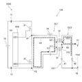
- FIG. 1 is a circuit diagram of a power supply device according to a first embodiment of the present invention.
- 2 is a timing chart of the circuit shown in FIG. It is a figure explaining operation
- FIG. 3 is a diagram illustrating an operation when the circuit shown in FIG. 1 is in a second state (when the second gate drive GD2 is in an on operation and the first gate drive GD1 is in an off operation).
- FIG. 1 does not function properly. It is a timing chart for demonstrating the flowing electric current.
- A Timing chart for explaining the case where the resonance circuit included in the circuit shown in FIG. 1 is functioning properly.
- B The resonance circuit included in the circuit shown in FIG. 1 is not functioning properly.
- 2 is a timing chart for explaining the case,
- c a timing chart in which a part of FIG. 1B is enlarged. It is the result of having simulated the magnetic flux density of the leakage magnetic field produced when an electric current is sent through the coil which has an air gap part in a magnetic core. It is the result of having simulated the Joule loss density based on a leakage magnetic field about the coil shown by FIG.
- FIG. 12 is a diagram for explaining an operation when the circuit shown in FIG. 11 is in a first state (when the first gate drive GD1 is on and the second gate drive GD2 is off).
- FIG. 12 is a diagram illustrating an operation when the circuit shown in FIG. 11 is in a second state (when the second gate drive GD2 is on and the first gate drive GD1 is off). It is a circuit diagram of the power supply device which concerns on 4th Embodiment of this invention.
- FIG. 12 is a diagram for explaining an operation when the circuit shown in FIG. 11 is in a first state (when the first gate drive GD1 is on and the second gate drive GD2 is off).
- FIG. 12 is a diagram illustrating an operation when the circuit shown in FIG. 11 is in a second state (when the second gate drive GD2 is on and the first gate drive GD1 is off).
- FIG. 12 is a diagram illustrating an operation when the circuit shown in FIG. 11 is in a second state (when the second gate drive GD2
- FIG. 15 is a diagram for explaining an operation when the circuit shown in FIG. 14 is in the first state (when the first gate drive GD1 is on and the second gate drive GD2 is off).
- FIG. 15 is a diagram for explaining an operation when the circuit shown in FIG. 14 is in a second state (when the second gate drive GD2 is on and the first gate drive GD1 is off).
- FIG. 1 is a circuit diagram of a power supply device according to the first embodiment of the present invention.
- the power supply device 100 according to the first embodiment of the present invention includes a DC voltage conversion circuit 10 and a first input terminal 11 and a second input terminal 12 included in the DC voltage conversion circuit 10. And a DC power supply 70 electrically connected.
- the positive terminal of the DC power supply 70 is connected to the first input terminal 11, and the negative terminal of the DC power supply 70 is connected to the second input terminal 12.
- the negative terminal of the DC power supply 70 may be connected to the ground terminal, and the second input terminal 12 may be grounded.
- the DC voltage conversion circuit 10 includes a plurality of switches. Specifically, in this embodiment, the DC voltage conversion circuit 10 includes a first switch 21, a second switch 22, a third switch 23, and a fourth switch 24. Each of these switches is a switch having a field effect transistor. One end of each of the first switch 21 and the third switch 23 is connected in parallel to the first input terminal 11. One end of each of the second switch 22 and the fourth switch 24 is connected in parallel to the second input terminal 12. The other end of the first switch 21 and the other end of the second switch 22 are connected, and the first switch 21 and the second switch 22 constitute a series connection (half-bridge circuit).
- the DC voltage conversion circuit 10 includes a first connection of the first input terminal 11 and a second connection of the first switch 21 and the second switch 22 and a second connection of the third switch 23 and the fourth switch 24.
- the input terminal 12 is connected in parallel (full bridge circuit).
- the DC voltage conversion circuit 10 is a series circuit unit in which a capacitor 33, a primary side 311 of a first transformer 31 and a primary side 321 of a second transformer 32 having the same polarity and magnetically independent from the first transformer 31 are connected in series. SC1 is provided.
- the capacitor 33 is a DC cut capacitor, and prevents a large direct current from flowing into the series circuit unit SC1 and a plurality of switches (from the first switch 21 to the fourth switch 24).
- a coil 34 is further connected to the series connection including the capacitor 33, the primary side 311 of the first transformer 31 and the primary side 321 of the second transformer 32. Are connected in series.
- first end portion P1 of the series circuit portion SC1 is connected between the first switch 21 and the second switch 22 connected in series, and the other end portion (first end) of the series circuit portion SC1.
- the two end portions P2) are connected between the third switch 23 and the fourth switch 24 connected in series.
- the DC voltage conversion circuit 10 includes a secondary side 312 of the first transformer 31 and a first rectifier diode 41 connected in series, and a first output terminal 51 is provided at the end of the first rectifier diode 41 in the rectification direction. 1 output circuit OC1 is provided.
- the output voltage Vout of the first output circuit OC1 is a potential difference of the first output terminal 51 with respect to the second output terminal 52 provided at the end opposite to the rectification direction of the first rectifier diode 41.
- the second output terminal 52 may be a ground terminal.
- the DC voltage conversion circuit 10 includes a secondary side 322 of the second transformer 32 and a second rectifier diode 42 connected in series, and the first output terminal 51 is connected to an end of the second rectifier diode 42 in the rectification direction.
- the end of the second rectifier diode 42 opposite to the rectifying direction is connected to the second output terminal 52 described above. Therefore, the first output circuit OC1 and the second output circuit OC2 share outputs (the first output terminal 51 and the second output terminal 52).
- the secondary side 312 of the first transformer 31 and the secondary side 322 of the second transformer 32 are connected in series, and the first output terminal 51 is connected to the secondary side 312 of the first transformer 31. This is a terminal for outputting a potential between the secondary transformer 322 and the secondary side 322.
- the DC voltage conversion circuit 10 includes a control unit 60 that controls a plurality of switches (the first switch 21 to the fourth switch 24).
- the control unit 60 includes two pulse drive circuits (a first gate drive GD1 and a second gate drive GD2), and the first gate drive GD1 and the second gate drive GD2 are independent of an ON / OFF (OFF) signal. Is output.
- the first gate drive GD1 synchronously controls the first switch 21 and the fourth switch 24, and the second gate drive GD2 synchronously controls the second switch 22 and the third switch 23.
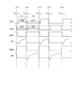
- FIG. 2 is a timing chart of the circuit shown in FIG.
- the control unit 60 alternately controls the first switch 21 and the second switch 22 on and off with a dead time period dt. If it demonstrates concretely based on FIG. 2, the 1st switch 21 will be controlled (the 3rd switch 23 is also synchronously controlled).
- the first gate drive GD1 is off from time t0 to time t1, is on from time t1 to time t2, and is off from time t2 to time t5. Thereafter, similarly, from time t5 to time t6 is on, from time t6 to time t9 is off, and after time t9 is on.
- the second switch 22 is controlled (the fourth switch 24 is also synchronously controlled).
- the second gate drive GD2 is off from time t0 to time t3 and is on from time t3 to time t4. Thereafter, similarly, from time t4 to time t7 and from time t8 to time t9 and thereafter are off, and from time t7 to time t8 are on. Accordingly, the dead time period dt is between time t0 and time t1, between time t2 and time t3, between time t4 and time t5, between time t6 and time t7, and between time t8 and time t9. Between.
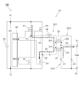
- FIG. 3 is a diagram for explaining the operation when the circuit shown in FIG. 1 is in the first state ST1 (when the first gate drive GD1 is on and the second gate drive GD2 is off).
- the counter electromotive force is generated on the primary side 311 of the first transformer 31 and the primary side 321 of the second transformer 32 due to the current flowing through the series circuit unit SC1.
- an induced current flows in the first output circuit OC1 based on the induced electromotive force generated by the counter electromotive force (indicated by a black broken line arrow B1 in FIG. 3).
- the second output circuit OC2 includes the second rectifier diode 42 that allows current to flow only from the second output terminal 52 side to the first output terminal 51 side, the second output circuit including the secondary side 322 of the second transformer 32. No induced current flows through OC2. Since the first transformer 31 and the second transformer 32 are magnetically independent, energy based on the counter electromotive force is accumulated in the second transformer 32.
- the drain voltage Vds2 of the second switch 22 increases in the dead time period dt between time t0 and time t1, and the second switch 22 is non-conductive. It becomes a state. For this reason, the drain current Id2 of the second switch 22, which has increased until time t0, becomes 0A at time t0.
- the second gate drive GD2 is kept off, whereas the first gate drive GD1 is turned off from on, so that the dead time period dt between time t2 and time t3 is increased. Be started.
- a resonance circuit is configured including the output capacitances of the first switch 21 and the third switch 23 (drain-source capacitances in the field effect transistor) and the inductance elements (the coil 34 and the second transformer 32).
- the voltage fluctuation based on the resonance of the resonance circuit is superimposed on the drain voltage Vds2 of the second switch 22 in the dead time period dt between the time t2 and the time t3, thereby realizing zero volt switching.
- the drain current Id2 of the second switch 22 temporarily becomes a negative current because a current based on this resonance circuit is superimposed. This point will be described later.
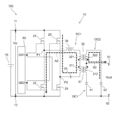
- FIG. 4 is a diagram for explaining the operation when the circuit shown in FIG. 1 is in the second state ST2 (when the second gate drive GD2 is on and the first gate drive GD1 is off).
- the back electromotive force is also generated on the primary side 311 of the first transformer 31 and the primary side 321 of the second transformer 32 by the current flowing through the series circuit unit SC1.
- an induced current flows in the second output circuit OC2 based on the induced electromotive force generated by the counter electromotive force (indicated by a black broken line arrow B2 in FIG. 4).
- the first output circuit OC1 includes the first rectifier diode 41 that allows current to flow only from the second output terminal 52 side to the first output terminal 51 side, the first output circuit including the secondary side 312 of the first transformer 31. No induced current flows through OC1. Since the first transformer 31 and the second transformer 32 are magnetically independent, energy based on the counter electromotive force is accumulated in the first transformer 31.
- the control unit 60 when the DC voltage is applied between the first input terminal 11 and the second input terminal 12, the control unit 60 performs the first switch. By alternately turning on and off 21 and the second switch 22 with a dead time period dt, the direction of the current flowing through the series circuit portion SC1 is alternately reversed. Under the control of the control unit 60, the first state ST1 and the second state ST2 occur alternately.
- the first switch 21 and the fourth switch 24 are on, current flows in the rectification direction of the first rectifier diode 41 in the first output circuit OC1 (black broken line arrow B1), and the second transformer 32 Electric energy is accumulated in
- the second switch 22 and the third switch 23 are on, and current flows in the rectification direction of the second rectifier diode 42 in the second output circuit OC2 (black broken line arrow B2), and the first transformer 31 Electric energy is accumulated in In the DC voltage conversion circuit 10 according to the first embodiment, as shown in FIG. 2, all periods in which the first switch 21 and the fourth switch 24 are on are in the first state ST1, and the second switch 22 and the second switch 22 All periods during which the 3 switch 23 is on are in the second state ST2.
- the control unit 60 changes at least one of the duty ratio D1 of the first switch 21 and the duty ratio D2 of the second switch 22, whereby the first output terminal 51 The potential difference (output voltage Vout) with respect to the second output terminal 52 can be changed.
- the duty ratio D1 of the first switch 21 and the duty ratio D2 of the second switch 22 satisfy the following conditions. 0 ⁇ D1 ⁇ 1, 0 ⁇ D2 ⁇ 1, D1 ⁇ D2 and 0 ⁇ D1 + D2 ⁇ 1
- the series circuit portion SC1 has a black broken line arrow A1 between the first end portion P1 and the second end portion P2.
- the series circuit portion SC1 is provided with a capacitor 33 that is a DC cut capacitor so that no current flows in the direction (in the case of D1> D2) or in the direction of the black broken line arrow A2 (in the case of D1 ⁇ D2).
- the dead time period dt provided after the period in which the first switch 21 and the fourth switch 24 are on is sufficiently shorter than the period in which the first switch 21 and the fourth switch 24 are on, and the second switch 22
- the output voltage Vout satisfies the following expression.
- FIG. 5A is a timing chart for explaining the current flowing through the series circuit portion of the circuit shown in FIG.
- FIG. 5B is a timing chart for explaining the current flowing through the series circuit section when the resonance circuit included in the circuit shown in FIG. 1 does not function properly.
- the upper current chart in FIG. 5A is the drain current Id1 of the first switch 21 shown in FIG. 2, and the middle current chart in FIG. 5A is the current chart of the second switch 22 shown in FIG.
- the polarity of the drain current Id2 is inverted. Since these currents flow in the series circuit portion SC1, if the flow from the first end P1 side to the second end P2 side is positive, the current chart on the upper side of FIG. 5A and FIG.
- a current chart obtained by synthesizing the current chart with the central current is a chart of the combined current Isc flowing through the series circuit portion SC1, and is shown on the lower side of FIG.
- the combined current Isc is gradually increased or decreased by the inductance elements (coil 34, first transformer 31 and second transformer 32) located in the series circuit section SC1. Yes.
- the inductance elements coil 34, first transformer 31, second transformer 32 located in series circuit section SC1 do not function properly, as shown in FIG. 5B, the combined current Isc is the first gate. It changes abruptly according to the operation of the drive GD1 and the second gate drive GD2.
- FIG. 6A is a timing chart for explaining a case where the resonance circuit included in the circuit shown in FIG. 1 is functioning properly
- FIG. 6B is an appropriate illustration of the resonance circuit included in the circuit shown in FIG. It is a timing chart for explaining a case where it does not function
- (c) is a timing chart in which a part of FIG.
- the drain voltage Vds1 of the first switch 21 becomes 0 V or less, the drain current Id1 flows in the negative direction, and zero volt switching is realized.
- the first transformer 31 or the second transformer 32 may be a part of the resonance circuit.
- the timing ton at which the field effect transistor constituting the one switch 21 is turned on is later than the time constant ⁇ , so that zero volt switching is not realized, and the drain voltage Vds1 of the first switch 21 is spiked. Voltage rise (surge voltage) occurs, and this voltage rise can cause noise.
- the inductance of the inductance element of the resonance circuit is large. From this viewpoint, the coil 34 is provided.
- an output circuit for example, the first transformer 31
- the primary side (primary side 321 of the second transformer 32) can function as an inductor, like the coil 34.
- the DC voltage conversion circuit 10 when the DC voltage conversion circuit 10 is applied to a display device such as a liquid crystal display device or an organic EL display device, or a power supply device for information equipment, noise should be suppressed. Preferably, zero volt switching as shown in a) is achieved.
- the DC voltage conversion circuit 10 is less affected by noise, such as a power supply device for a charging station of an electric vehicle, it is not particularly required that zero volt switching be performed.
- a spike voltage (surge voltage) or a spike current is generated as shown in FIGS. 6B and 6C due to the discharge of charges accumulated in the output capacitance of the switch. (Surge current) may occur (hard switching).
- the control range of the DC voltage conversion circuit 10 can be expanded. Further, since the coil 34 is not essential in the DC voltage conversion circuit 10, the DC voltage conversion circuit 10 can be downsized.
- the DC voltage conversion circuit 10 Since the DC voltage conversion circuit 10 is a so-called full bridge system, the voltage applied to the series circuit unit SC1 is the input voltage Vin from the DC power supply 70 of the power supply device 100. For this reason, it is preferable to be used for high-power converter applications.
- the relationship between the output voltage Vout of the DC voltage conversion circuit 10 and the input voltage Vin is such that the duty ratio D1 (0 ⁇ D1 ⁇ 1) of the pulse output from the pulse drive circuit and the turns ratio of the transformer (primary side turns /
- the secondary winding number n is expressed as follows (however, the winding ratio of the first transformer 31 and the winding ratio of the second transformer 32 are equal).
- Vout 2 ⁇ D1 ⁇ (1-D1) ⁇ Vin / n
- the DC voltage conversion circuit 10 does not necessarily have a high step-down ratio (Vout / Vin) as a DC-DC converter, but the current flowing through the switches such as the first switch 21 is relatively low, so that it is suitable for high output applications. Yes.
- the DC voltage conversion circuit 10 is suitable for high-power applications, but constitutes a magnetic core (core) of an inductance element (coil 34, first transformer 31, second transformer 32).
- a general ferrite soft magnetic material is applied as a material from the viewpoint of low core loss in a high frequency (for example, 100 kHz or more) application, the following problems are concerned.
- the transformer whose secondary side is located in the output circuit where current does not flow during operation functions as an energy storage element like the coil 34.
- the transformer core is preferably made of a material that is less likely to cause magnetic saturation, but the ferrite-based soft magnetic material has a relatively high magnetic permeability.
- the air gap part causes a problem of leakage magnetic flux, resulting in an increase in the loss of the transformer core (including copper loss).
- the ferrite-based soft magnetic material since the ferrite-based soft magnetic material has a relatively low saturation magnetic flux density, it is necessary to increase the volume of the transformer core in order to avoid magnetic saturation, which is an obstacle to miniaturization of the transformer. It was.
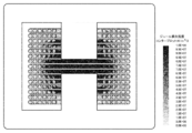
- FIG. 7 is a result of simulating a magnetic flux (leakage magnetic flux) of a leakage magnetic field generated when a current is passed through a coil having an air gap portion in the magnetic core.
- FIG. 8 is a simulation of Joule loss density based on the leakage magnetic flux. It is a result.
- magnetic flux leaks from the air gap portion, and a part of the leakage magnetic flux passes through a coil positioned around the air gap. Due to the leakage magnetic flux from the air gap portion, an induced current flows through the coil and Joule loss occurs.
- FIG. 8 since the density of the Joule loss increases around the air gap portion, when the coil having the air gap portion in the magnetic core is downsized, the coil is excessively heated based on the Joule loss. There is a concern that the coil will deteriorate in function.
- the permeability (initial permeability) of the magnetic core (core) of the transformer is 15 or more and 120 or less. Is set. When the permeability of the magnetic core of the transformer is in this range, the magnetization of the transformer is less likely to be saturated and energy loss is less likely to occur without providing an air gap portion in the transformer.
- the magnetic permeability (core) of the transformer is more preferably 20 or more and 80 or less, and particularly preferably 25 or more and 60 or less.
- the magnetic permeability of ferrite such as MnZn-based ferrite which is a typical example of a soft magnetic material constituting the magnetic core (core) of the transformer, is 1000 to 3500, for example. If it is intended to set the magnetic permeability (effective magnetic permeability) of the transformer core (core) within the above range using such a material, it is necessary to provide an air gap portion. There is a concern about the influence of leakage magnetic flux. Therefore, it is preferable that the transformers (the first transformer 31 and the second transformer 32) included in the DC voltage conversion circuit 10 do not have an air gap portion.
- the saturation magnetic flux density of the magnetic core (core) of the transformer is 700 mT or more. This is preferable from the viewpoint of avoiding magnetic saturation of the magnetic core.
- the saturation magnetic flux density of the magnetic core (core) of the transformer is more preferably 0.9 T or more, and particularly preferably 1.1 T or more.
- the upper limit of the saturation magnetic flux density of the magnetic core (core) of the transformer is not defined.
- a magnetic material having a saturation magnetic flux density of 1.4 T or more may have a strong tendency to deteriorate the loss characteristics, so it may be preferable to set the upper limit to about 1.3 T.
- the saturation magnetic flux density of the transformer core is 0.8 to 1.3 T. From the viewpoint of securing the availability of the material constituting the magnetic core (core) of the transformer, it may be preferable to set it to about 1.2 T or less.
- the saturation magnetic flux density of a ferrite-based soft magnetic material which is a typical example of the soft magnetic material constituting the transformer core, is generally 380 mT to 500 mT.
- the magnetic material used for the magnetic core (core) of the transformer is easy because it is easy to satisfy the preferred range regarding the magnetic permeability and the preferred range of the saturation magnetic flux density. It is preferable to use an amorphous metal soft magnetic material or a nanocrystalline metal soft magnetic material.
- a specific example of the amorphous metal-based soft magnetic material is an Fe—PC-based amorphous magnetic alloy.
- a dust core made of Fe—PC—C amorphous magnetic alloy powder has a low magnetic permeability (120 or less), a high saturation magnetic flux density (700 mT or more), and a high frequency (eg, 100 kHz or more), and This is preferable because a low core loss can be realized.
- the magnetic core (core) of the coil 34 is also preferably 15 or more and 120 or less, and 20 or more. It is more preferably 80 or less, and particularly preferably 25 or more and 60 or less. If the magnetic core (core) of the coil 34 is air gapless, it is preferable because no leakage magnetic flux is generated.
- the saturation magnetic flux density of the magnetic core (core) of the coil 34 is preferably 700 mT or more, more preferably 0.9 T or more, and particularly preferably 1.1 T or more. From the viewpoint of meeting such demands, it is preferable that the magnetic core (core) of the coil 34 is made of an amorphous metal soft magnetic material or a nanocrystalline metal soft magnetic material. The same as in the case of (core).
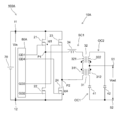
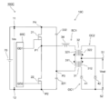
- FIG. 9 is a circuit diagram of a power supply device according to the second embodiment of the present invention.
- the circuit configuration of the DC voltage conversion circuit 10A included in the power supply device 100A according to the second embodiment of the present invention is the same as that of the power supply device 100 according to the first embodiment of the present invention shown in FIG.
- the circuit configuration of the DC voltage conversion circuit 10 provided is common except for the configuration of the control unit 60A.
- the control unit 60A of the DC voltage conversion circuit 10A includes a first gate drive GD1 that controls the first switch 21, a second gate drive GD2 that controls the second switch 22, and a third gate drive GD3 that controls the third switch 23. And a fourth gate drive GD4 for controlling the fourth switch 24.
- the circuit configuration of the DC voltage conversion circuit 10A is the same as that of the DC voltage conversion circuit 10 except for the configuration of the control unit 60A, only the control unit 60A will be described below, and other circuit configurations in the DC voltage conversion circuit 10A will be described. The description of is omitted. Note that the capacitor 33 is not essential in the DC voltage conversion circuit 10A. This point will be described later.
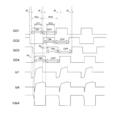
- FIG. 10 is a timing chart of the DC voltage conversion circuit 10A included in the power supply device 100A according to the second embodiment of the present invention shown in FIG.
- the timing chart of the first gate drive GD1 to the fourth gate drive GD4 the drain current Id1 of the first switch 21, the drain current Id4 of the fourth switch 24, and the drain voltage Vds4 of the fourth switch are shown. Has been.
- the control unit 60A of the DC voltage conversion circuit 10A alternately turns on and off the first switch 21 and the second switch 22 with a dead time period dt, and also performs the dead time period for the third switch 23 and the fourth switch 24. It is common to the control unit 60 of the DC voltage conversion circuit 10 according to the first embodiment in that it has dt and performs on / off control alternately. In the first embodiment, the first switch 21 and the fourth switch 24 are on in the first state ST1, and the second switch 22 and the third switch 23 are on in the second state ST2. The control is the same as that of the control unit 60 of the DC voltage conversion circuit 10.
- control unit 60A of the DC voltage conversion circuit 10A according to the second embodiment differs from the control unit 60 of the DC voltage conversion circuit 10 according to the first embodiment in that the first switch 21 and Synchronous control with the fourth switch 24 and synchronous control between the second switch 22 and the third switch 23 are not performed, and so-called phase shift control is performed on the first switch 21 to the fourth switch 24.
- the control unit 60A causes each of the first switch 21 to the fourth switch 24 to have an equal duty less than 0.5.
- ON and OFF are repeated at the ratio D.
- the total period of the on period Pon which is the period in the on state
- the off period Poff which is the period in the off state
- the duty ratio D is less than 0.5 because the dead time period dt is provided before and after the ON period Pon of each switch.
- the control unit 60A controls the second switch 22 to turn on the fourth switch 24 so that the timing to turn on the first switch 21 is shifted.
- the fourth switch 24 is turned on and the first state ST1 is changed in response to the elapse of a shift period Ps that is a predetermined length shorter than the on period Pon. generate.
- a period in which the fourth switch 24, which is turned on with a phase shift with respect to the first switch 21, is ON and an ON period Pon related to the first switch 21 overlaps. Only the period is in the first state ST1, and not all the on periods Pon related to the first switch 21 are in the first state ST1.
- the second switch 22 is turned on when the dead time period dt has elapsed since the first switch 21 was turned off.
- the first state ST1 ends.
- the third switch 23 is turned on to generate the second state ST2.
- a period in which the third switch 23 which is turned on with a phase shift with respect to the second switch 22 is overlapped with an on period Pon related to the second switch 22. Only the period is in the second state ST2, and the entire on period Pon related to the second switch 22 is not in the second state ST2.
- the length of the period of the first state ST1 and the length of the period of the second state ST2 are changed, whereby the second output terminal 52 of the first output terminal 51 is controlled.
- the potential difference (output voltage Vout) is changed.
- the output voltage Vout is equal to the shift period Ps.
- the output voltage Vout can be adjusted by changing the length of the shift period Ps having the following relationship. Vout ⁇ Ps / (Pon + Poff) Here, 0 ⁇ Ps / (Pon + Poff) ⁇ 0.5.
- the DC voltage conversion circuit 10 provided in the power supply device 100 according to the first embodiment described above and the DC voltage conversion circuit 10A provided in the power supply device 100A according to the second embodiment, four switches (from the first switch 21 to the fourth switch) are provided. 24) constitutes a full bridge circuit.
- the DC voltage conversion circuit 10 according to the first embodiment is a DC cut capacitor because the first switch 21 and the fourth switch 24 are synchronously controlled and the second switch 22 and the third switch 23 are synchronously controlled.
- a capacitor 33 is provided to prevent a large current from flowing into the series circuit portion SC1.
- the four switches having the same duty ratio D are on / off controlled with the phase shifted, and thus the series circuit portion SC1 has a large amount. Current does not flow easily. For this reason, in the DC voltage conversion circuit 10A according to the second embodiment, it is not essential to provide the capacitor 33, which is a DC cut capacitor, in the series circuit unit SC1.
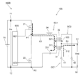
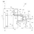
- FIG. 11 is a circuit diagram of a power supply device according to the third embodiment of the present invention.
- FIG. 12 is a diagram for explaining the operation when the circuit shown in FIG. 11 is in the first state ST1 (when the first gate drive GD1 is on and the second gate drive GD2 is off).
- FIG. 13 is a diagram for explaining the operation when the circuit shown in FIG. 11 is in the second state ST2 (when the second gate drive GD2 is on and the first gate drive GD1 is off).
- the full bridge circuit including four switches in the DC voltage conversion circuit 10 according to the first embodiment is replaced with a half bridge circuit including two switches. Is. If the DC voltage conversion circuit 10B according to the third embodiment is described in comparison with the DC voltage conversion circuit 10 according to the first embodiment, the third switch 23 and the fourth switch 24 in the DC voltage conversion circuit 10 are connected in series. The other half portion (second end portion P2) of the series circuit portion SC1 is connected between the second switch 22 and the second input terminal 12.
- the first capacitor 331 is provided at a position where the capacitor 33 which is a DC cut capacitor is provided in the DC voltage conversion circuit 10 according to the first embodiment. That is, the primary side 311 of the first transformer 31 and the primary 321 side of the second transformer 32 and the first capacitor 331 are connected in series, and the first switch 21 is connected in series to this series connection.
- the first capacitor 331 includes a series connection composed of the primary side 311 of the first transformer 31 and the primary 321 side of the second transformer 32, and the other end of the series circuit unit SC ⁇ b> 1 (second It is located between the ends P2), but is not limited to this.
- the first capacitor 331 only needs to be connected in series to the series connection formed by the primary side 311 of the first transformer 31 and the primary 321 side of the second transformer 32.
- the first capacitor 331 includes a serial connection composed of the primary side 311 of the first transformer 31 and the primary 321 side of the second transformer 32, and one end portion (first end portion P1) of the series circuit portion SC1. It may be located between.
- the coil 34 is also connected in series with the series connection formed by the primary side 311 of the first transformer 31 and the primary 321 side of the second transformer 32.
- the control unit 60B of the DC voltage conversion circuit 10B according to the third embodiment performs the same control as the control unit 60 of the DC voltage conversion circuit 10 according to the first embodiment. That is, the first switch 21 and the second switch 22 are alternately turned on / off with a dead time period dt. Further, the potential difference (output voltage Vout) of the first output terminal 51 with respect to the second output terminal 52 can be changed by changing at least one of the duty ratio D1 of the first switch 21 and the duty ratio D2 of the second switch 22. It is. Since the duty ratio D1 of the first switch 21 and the duty ratio D2 of the second switch 22 are not equal (asymmetric), a DC cut capacitor for preventing a large current from flowing into the series circuit unit SC1 is necessary. In the voltage conversion circuit 10B, the first capacitor 331 performs its function. A capacitor 33 as a DC cut capacitor may be provided separately from the first capacitor 331.
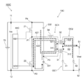
- FIG. 14 is a circuit diagram of a power supply device according to the fourth embodiment of the present invention.
- FIG. 15 is a diagram for explaining the operation when the circuit shown in FIG. 14 is in the first state ST1 (when the first gate drive GD1 is on and the second gate drive GD2 is off).
- FIG. 16 is a diagram for explaining the operation when the circuit shown in FIG. 14 is in the second state ST2 (when the second gate drive GD2 is on and the first gate drive GD1 is off).
- the DC voltage conversion circuit 10C included in the power supply device 100C according to the fourth embodiment is compared with the DC voltage conversion circuit 10B included in the power supply device 100B according to the third embodiment, and the series circuit unit SC1 includes the first transformer 31.
- a second capacitor 332 is further provided that is connected in series to the series connection formed by the primary 311 side and the primary 321 side of the second transformer 32.
- the second switch 22 is connected in series to the serial connection composed of the primary 311 side of the first transformer 31 and the primary 321 side of the second transformer 32 and the second capacitor 332 thus configured.
- the coil 34 is also connected in series with the series connection formed by the primary side 311 of the first transformer 31 and the primary 321 side of the second transformer 32.
- the first capacitor 331 includes a serial connection composed of the primary 311 side of the first transformer 31 and the primary 321 side of the second transformer 32 and the other end portion (second end portion P2) of the series circuit portion SC1. ).
- One end portion (third end portion P3) of the second capacitor 332 is connected between the first capacitor 311, and the series connection formed by the primary 311 side of the first transformer 31 and the primary 321 side of the second transformer 32.
- the other end (fourth end P4) of the second capacitor 332 is connected to the first input terminal 11. Therefore, the first capacitor 331 and the second capacitor 332 are connected in series, and this series connection is located between the first input terminal 11 and the second input terminal 12. That is, the DC voltage conversion circuit 10C according to the fourth embodiment is provided with a second capacitor 332 instead of the third switch 23 in contrast to the DC voltage conversion circuit 10 according to the first embodiment, and the fourth switch 24. Instead, the first capacitor 331 is provided.
- the current from the first input terminal 11 is connected in series including the primary 311 side of the first transformer 31, the primary 321 side of the second transformer 32, and the first switch 21.
- a current path black broken line arrow A11
- the electric charge accumulated in the second capacitor 332 is released, and the first transformer 31 is connected in series including the primary 311 side and the primary transformer 321 side of the second transformer 32, and the first switch 21 and the second capacitor 332 are closed.
- a current in the direction of the black dotted line arrow A12 flows through the circuit.
- a current flows through the first output circuit OC1 (black dashed arrow B1), and electrical energy is stored in the second transformer 32.
- the first transformer 31 has a primary 311 side, a primary 321 side of the second transformer 32, and a series connection including the first switch 21 and the second input terminal 12.
- Charge is accumulated in the second capacitor 332 by the current path (black broken arrow A21) through which the current flows.
- the electric charge accumulated in the first capacitor 331 is discharged, and includes a series connection including the primary 311 side of the first transformer 31 and the primary 321 side of the second transformer 32, the second switch 22 and the first capacitor 331.
- a current in the direction of the black dotted line arrow A22 flows in the closed circuit.
- a current flows through the second output circuit OC2 (black broken arrow B2), and electrical energy is stored in the first transformer 31.
- the control unit 60C of the DC voltage conversion circuit 10C according to the fourth embodiment performs the same control as the control unit 60 of the DC voltage conversion circuit 10 according to the first embodiment. That is, the first switch 21 and the second switch 22 are alternately turned on / off with a dead time period dt. Further, the potential difference (output voltage Vout) of the first output terminal 51 with respect to the second output terminal 52 can be changed by changing at least one of the duty ratio D1 of the first switch 21 and the duty ratio D2 of the second switch 22. It is. Since the duty ratio D1 of the first switch 21 and the duty ratio D2 of the second switch 22 are not equal (asymmetric), a DC cut capacitor for preventing a large current from flowing into the series circuit unit SC1 is necessary. In the voltage conversion circuit 10B, the first capacitor 331 and the second capacitor 332 fulfill their functions. A capacitor 33 as a DC cut capacitor may be provided separately from the first capacitor 331 and the second capacitor 332.
- the inductor such as the coil 34 forms a resonance circuit with the output capacitors of the plurality of switches (the first switch 21 to the fourth switch 24).
- the maximum amplitude voltage of the resonance circuit is set to be larger than the drain voltage of the switch and zero volt switching is performed, the present invention is not limited to this.
- a device provided with a DC power supply conversion circuit is applied to a power supply device for a display device or an information device, it is preferable to realize zero volt switching to suppress noise generation.
- the coil 34 provided in the series circuit unit SC1 is not necessary in the DC power supply conversion circuit according to the above embodiment.
- the DC voltage conversion circuit according to an embodiment of the present invention can be suitably used as a partial circuit of a high-power switching power supply.
Landscapes
- Engineering & Computer Science (AREA)
- Power Engineering (AREA)
- Dc-Dc Converters (AREA)
Priority Applications (4)
| Application Number | Priority Date | Filing Date | Title |
|---|---|---|---|
| CN201880091138.3A CN111869076B (zh) | 2018-03-20 | 2018-12-03 | 直流电压变换电路以及电源装置 |
| JP2020507342A JP6902673B2 (ja) | 2018-03-20 | 2018-12-03 | 直流電圧変換回路および電源装置 |
| US17/016,507 US11381174B2 (en) | 2018-03-20 | 2020-09-10 | DC voltage conversion circuit and power supply device |
| US17/848,720 US11581818B2 (en) | 2018-03-20 | 2022-06-24 | DC voltage conversion circuit and power supply device |
Applications Claiming Priority (2)
| Application Number | Priority Date | Filing Date | Title |
|---|---|---|---|
| JP2018053020 | 2018-03-20 | ||
| JP2018-053020 | 2018-03-20 |
Related Child Applications (2)
| Application Number | Title | Priority Date | Filing Date |
|---|---|---|---|
| US17/016,507 Continuation US11381174B2 (en) | 2018-03-20 | 2020-09-10 | DC voltage conversion circuit and power supply device |
| US17/016,507 Continuation-In-Part US11381174B2 (en) | 2018-03-20 | 2020-09-10 | DC voltage conversion circuit and power supply device |
Publications (1)
| Publication Number | Publication Date |
|---|---|
| WO2019181082A1 true WO2019181082A1 (ja) | 2019-09-26 |
Family
ID=67986088
Family Applications (1)
| Application Number | Title | Priority Date | Filing Date |
|---|---|---|---|
| PCT/JP2018/044428 Ceased WO2019181082A1 (ja) | 2018-03-20 | 2018-12-03 | 直流電圧変換回路および電源装置 |
Country Status (5)
| Country | Link |
|---|---|
| US (2) | US11381174B2 (cg-RX-API-DMAC7.html) |
| JP (2) | JP6902673B2 (cg-RX-API-DMAC7.html) |
| CN (1) | CN111869076B (cg-RX-API-DMAC7.html) |
| TW (1) | TWI717666B (cg-RX-API-DMAC7.html) |
| WO (1) | WO2019181082A1 (cg-RX-API-DMAC7.html) |
Cited By (1)
| Publication number | Priority date | Publication date | Assignee | Title |
|---|---|---|---|---|
| WO2026053573A1 (ja) * | 2024-09-06 | 2026-03-12 | 株式会社ダイヤメット | Pwm制御装置及び電源システム |
Families Citing this family (3)
| Publication number | Priority date | Publication date | Assignee | Title |
|---|---|---|---|---|
| CN110460242B (zh) * | 2019-09-12 | 2020-11-10 | 台达电子企业管理(上海)有限公司 | 双向隔离型谐振变换器 |
| EP4097834A1 (en) | 2020-01-30 | 2022-12-07 | The Board Of Trustees Of The University Of Illinois | Three phase ac/dc converter consisting of three single phase synchronous cuk converters |
| WO2025069933A1 (ja) * | 2023-09-27 | 2025-04-03 | 株式会社村田製作所 | Dc-dcコンバータ及びスイッチング電源装置 |
Citations (4)
| Publication number | Priority date | Publication date | Assignee | Title |
|---|---|---|---|---|
| JP2003272940A (ja) * | 2002-03-18 | 2003-09-26 | Nippon Chemicon Corp | 積層型コアの製造方法 |
| JP2008054378A (ja) * | 2006-08-22 | 2008-03-06 | Toshiba Corp | Dc−dcコンバータ |
| JP2009136137A (ja) * | 2007-10-30 | 2009-06-18 | Tdk Corp | スイッチング電源装置 |
| JP2016213383A (ja) * | 2015-05-12 | 2016-12-15 | パナソニックIpマネジメント株式会社 | 磁気部品及びこれを用いた電源回路 |
Family Cites Families (15)
| Publication number | Priority date | Publication date | Assignee | Title |
|---|---|---|---|---|
| JPS5238387A (en) | 1975-09-19 | 1977-03-24 | Olympic Fishing Tackles Co | Spool position adjusting apparatus for angling reels |
| JPH02188904A (ja) * | 1989-01-17 | 1990-07-25 | Kyushu Univ | 偏磁防止変圧器 |
| JP3069565B1 (ja) * | 1998-12-08 | 2000-07-24 | 松下電器産業株式会社 | スイッチング電源装置 |
| US6151222A (en) | 1999-03-02 | 2000-11-21 | Delco Electronics Corp. | Dual voltage automotive electrical system with sub-resonant DC-DC converter |
| JP5004260B2 (ja) * | 2000-02-21 | 2012-08-22 | 日立金属株式会社 | 外鉄型パワートランスおよびこれを用いた電力変換装置 |
| JP2001268906A (ja) * | 2000-03-01 | 2001-09-28 | Delphi Technol Inc | サブ共振dc−dcコンバータを有するデュアル電圧自動車両電気システム |
| JP4352444B2 (ja) * | 2000-09-19 | 2009-10-28 | Tdkラムダ株式会社 | 共振コンバータ |
| KR20080011425A (ko) | 2005-06-02 | 2008-02-04 | 가부시키가이샤 시세이도 | 붕괴성 산화아연 분체 및 그 제조 방법 |
| JP4649299B2 (ja) * | 2005-09-07 | 2011-03-09 | 株式会社東芝 | Dc−dcコンバータ |
| JP4378400B2 (ja) * | 2007-08-28 | 2009-12-02 | 日立コンピュータ機器株式会社 | 双方向dc−dcコンバータ及び双方向dc−dcコンバータの制御方法 |
| US7623362B2 (en) | 2007-10-30 | 2009-11-24 | Tdk Corporation | Switching power supply unit |
| JP5050874B2 (ja) * | 2008-01-22 | 2012-10-17 | 富士電機株式会社 | スイッチング電源装置 |
| JP4806455B2 (ja) * | 2009-03-27 | 2011-11-02 | 株式会社日立メディアエレクトロニクス | スイッチング電源およびスイッチング方法 |
| JP5447507B2 (ja) * | 2009-04-14 | 2014-03-19 | 株式会社村田製作所 | スイッチング電源装置 |
| JP2015012147A (ja) * | 2013-06-28 | 2015-01-19 | 株式会社オートネットワーク技術研究所 | リアクトル |
-
2018
- 2018-12-03 CN CN201880091138.3A patent/CN111869076B/zh active Active
- 2018-12-03 JP JP2020507342A patent/JP6902673B2/ja active Active
- 2018-12-03 WO PCT/JP2018/044428 patent/WO2019181082A1/ja not_active Ceased
- 2018-12-14 TW TW107145132A patent/TWI717666B/zh active
-
2020
- 2020-09-10 US US17/016,507 patent/US11381174B2/en active Active
-
2021
- 2021-06-18 JP JP2021101838A patent/JP2021168590A/ja not_active Withdrawn
-
2022
- 2022-06-24 US US17/848,720 patent/US11581818B2/en active Active
Patent Citations (4)
| Publication number | Priority date | Publication date | Assignee | Title |
|---|---|---|---|---|
| JP2003272940A (ja) * | 2002-03-18 | 2003-09-26 | Nippon Chemicon Corp | 積層型コアの製造方法 |
| JP2008054378A (ja) * | 2006-08-22 | 2008-03-06 | Toshiba Corp | Dc−dcコンバータ |
| JP2009136137A (ja) * | 2007-10-30 | 2009-06-18 | Tdk Corp | スイッチング電源装置 |
| JP2016213383A (ja) * | 2015-05-12 | 2016-12-15 | パナソニックIpマネジメント株式会社 | 磁気部品及びこれを用いた電源回路 |
Cited By (1)
| Publication number | Priority date | Publication date | Assignee | Title |
|---|---|---|---|---|
| WO2026053573A1 (ja) * | 2024-09-06 | 2026-03-12 | 株式会社ダイヤメット | Pwm制御装置及び電源システム |
Also Published As
| Publication number | Publication date |
|---|---|
| CN111869076A (zh) | 2020-10-30 |
| CN111869076B (zh) | 2023-10-03 |
| TW201941528A (zh) | 2019-10-16 |
| JP2021168590A (ja) | 2021-10-21 |
| JP6902673B2 (ja) | 2021-07-14 |
| US20220321015A1 (en) | 2022-10-06 |
| US11581818B2 (en) | 2023-02-14 |
| US20200412261A1 (en) | 2020-12-31 |
| JPWO2019181082A1 (ja) | 2020-10-22 |
| US11381174B2 (en) | 2022-07-05 |
| TWI717666B (zh) | 2021-02-01 |
Similar Documents
| Publication | Publication Date | Title |
|---|---|---|
| US11641164B2 (en) | Power conversion circuit and power conversion apparatus with same | |
| JP5434370B2 (ja) | 共振型スイッチング電源装置 | |
| US8009444B2 (en) | Boost device for voltage boosting | |
| CN104981971B (zh) | 正反激拓扑的开关模式电源 | |
| CN103490629B (zh) | 开关模式电源和两阶段dc到dc转换器 | |
| US7405955B2 (en) | Switching power supply unit and voltage converting method | |
| JP2021168590A (ja) | 直流電圧変換回路および電源装置 | |
| JP6241334B2 (ja) | 電流共振型dcdcコンバータ | |
| TWI763720B (zh) | 用於將輸入電壓轉換成輸出電壓的功率轉換器及方法 | |
| US20100328971A1 (en) | Boundary mode coupled inductor boost power converter | |
| JP2005160217A (ja) | スイッチング電源装置 | |
| JP2013236531A (ja) | Llc直列共振コンバータ | |
| CN111492568B (zh) | 交错式llc谐振变换器 | |
| US11527959B2 (en) | Control method of power conversion device | |
| US20220209661A1 (en) | Power conversion device | |
| JP3202692U (ja) | 電力変換システム | |
| US9178435B2 (en) | Switching power supply | |
| US8854850B2 (en) | AC power supply apparatus | |
| KR101229265B1 (ko) | 집적 변압기 및 이를 이용한 고승압 직류-직류 컨버터 | |
| CN114568042A (zh) | 反激式转换器及其操作方法 | |
| TWM522514U (zh) | 電能轉換系統 | |
| KR102616665B1 (ko) | 위상천이 풀브리지 컨버터 및 그 구동방법 | |
| JP2015061342A (ja) | 電源回路および画像形成装置 | |
| CN120454478A (zh) | 基于变压器的驱动供电电路 | |
| JPH0686541A (ja) | スイッチング電源装置 |
Legal Events
| Date | Code | Title | Description |
|---|---|---|---|
| 121 | Ep: the epo has been informed by wipo that ep was designated in this application |
Ref document number: 18911066 Country of ref document: EP Kind code of ref document: A1 |
|
| ENP | Entry into the national phase |
Ref document number: 2020507342 Country of ref document: JP Kind code of ref document: A |
|
| NENP | Non-entry into the national phase |
Ref country code: DE |
|
| 122 | Ep: pct application non-entry in european phase |
Ref document number: 18911066 Country of ref document: EP Kind code of ref document: A1 |