WO2019175698A1 - 金属酸化物、及び金属酸化物を有するトランジスタ - Google Patents
金属酸化物、及び金属酸化物を有するトランジスタ Download PDFInfo
- Publication number
- WO2019175698A1 WO2019175698A1 PCT/IB2019/051595 IB2019051595W WO2019175698A1 WO 2019175698 A1 WO2019175698 A1 WO 2019175698A1 IB 2019051595 W IB2019051595 W IB 2019051595W WO 2019175698 A1 WO2019175698 A1 WO 2019175698A1
- Authority
- WO
- WIPO (PCT)
- Prior art keywords
- oxide
- layer
- insulator
- metal oxide
- transistor
- Prior art date
- Legal status (The legal status is an assumption and is not a legal conclusion. Google has not performed a legal analysis and makes no representation as to the accuracy of the status listed.)
- Ceased
Links
Images













Classifications
-
- H—ELECTRICITY
- H10—SEMICONDUCTOR DEVICES; ELECTRIC SOLID-STATE DEVICES NOT OTHERWISE PROVIDED FOR
- H10D—INORGANIC ELECTRIC SEMICONDUCTOR DEVICES
- H10D30/00—Field-effect transistors [FET]
- H10D30/60—Insulated-gate field-effect transistors [IGFET]
- H10D30/67—Thin-film transistors [TFT]
- H10D30/674—Thin-film transistors [TFT] characterised by the active materials
- H10D30/6755—Oxide semiconductors, e.g. zinc oxide, copper aluminium oxide or cadmium stannate
-
- C—CHEMISTRY; METALLURGY
- C01—INORGANIC CHEMISTRY
- C01G—COMPOUNDS CONTAINING METALS NOT COVERED BY SUBCLASSES C01D OR C01F
- C01G15/00—Compounds of gallium, indium or thallium
-
- H—ELECTRICITY
- H10—SEMICONDUCTOR DEVICES; ELECTRIC SOLID-STATE DEVICES NOT OTHERWISE PROVIDED FOR
- H10B—ELECTRONIC MEMORY DEVICES
- H10B12/00—Dynamic random access memory [DRAM] devices
-
- H—ELECTRICITY
- H10—SEMICONDUCTOR DEVICES; ELECTRIC SOLID-STATE DEVICES NOT OTHERWISE PROVIDED FOR
- H10B—ELECTRONIC MEMORY DEVICES
- H10B41/00—Electrically erasable-and-programmable ROM [EEPROM] devices comprising floating gates
- H10B41/70—Electrically erasable-and-programmable ROM [EEPROM] devices comprising floating gates the floating gate being an electrode shared by two or more components
-
- H—ELECTRICITY
- H10—SEMICONDUCTOR DEVICES; ELECTRIC SOLID-STATE DEVICES NOT OTHERWISE PROVIDED FOR
- H10D—INORGANIC ELECTRIC SEMICONDUCTOR DEVICES
- H10D30/00—Field-effect transistors [FET]
- H10D30/60—Insulated-gate field-effect transistors [IGFET]
- H10D30/62—Fin field-effect transistors [FinFET]
- H10D30/6212—Fin field-effect transistors [FinFET] having fin-shaped semiconductor bodies having non-rectangular cross-sections
- H10D30/6213—Fin field-effect transistors [FinFET] having fin-shaped semiconductor bodies having non-rectangular cross-sections having rounded corners
-
- H—ELECTRICITY
- H10—SEMICONDUCTOR DEVICES; ELECTRIC SOLID-STATE DEVICES NOT OTHERWISE PROVIDED FOR
- H10D—INORGANIC ELECTRIC SEMICONDUCTOR DEVICES
- H10D30/00—Field-effect transistors [FET]
- H10D30/60—Insulated-gate field-effect transistors [IGFET]
- H10D30/67—Thin-film transistors [TFT]
- H10D30/6704—Thin-film transistors [TFT] having supplementary regions or layers in the thin films or in the insulated bulk substrates for controlling properties of the device
- H10D30/6713—Thin-film transistors [TFT] having supplementary regions or layers in the thin films or in the insulated bulk substrates for controlling properties of the device characterised by the properties of the source or drain regions, e.g. compositions or sectional shapes
-
- H—ELECTRICITY
- H10—SEMICONDUCTOR DEVICES; ELECTRIC SOLID-STATE DEVICES NOT OTHERWISE PROVIDED FOR
- H10D—INORGANIC ELECTRIC SEMICONDUCTOR DEVICES
- H10D30/00—Field-effect transistors [FET]
- H10D30/60—Insulated-gate field-effect transistors [IGFET]
- H10D30/67—Thin-film transistors [TFT]
- H10D30/6729—Thin-film transistors [TFT] characterised by the electrodes
- H10D30/6737—Thin-film transistors [TFT] characterised by the electrodes characterised by the electrode materials
- H10D30/6739—Conductor-insulator-semiconductor electrodes
-
- H—ELECTRICITY
- H10—SEMICONDUCTOR DEVICES; ELECTRIC SOLID-STATE DEVICES NOT OTHERWISE PROVIDED FOR
- H10D—INORGANIC ELECTRIC SEMICONDUCTOR DEVICES
- H10D30/00—Field-effect transistors [FET]
- H10D30/60—Insulated-gate field-effect transistors [IGFET]
- H10D30/67—Thin-film transistors [TFT]
- H10D30/6757—Thin-film transistors [TFT] characterised by the structure of the channel, e.g. transverse or longitudinal shape or doping profile
-
- H—ELECTRICITY
- H10—SEMICONDUCTOR DEVICES; ELECTRIC SOLID-STATE DEVICES NOT OTHERWISE PROVIDED FOR
- H10D—INORGANIC ELECTRIC SEMICONDUCTOR DEVICES
- H10D30/00—Field-effect transistors [FET]
- H10D30/60—Insulated-gate field-effect transistors [IGFET]
- H10D30/68—Floating-gate IGFETs
-
- H—ELECTRICITY
- H10—SEMICONDUCTOR DEVICES; ELECTRIC SOLID-STATE DEVICES NOT OTHERWISE PROVIDED FOR
- H10D—INORGANIC ELECTRIC SEMICONDUCTOR DEVICES
- H10D30/00—Field-effect transistors [FET]
- H10D30/60—Insulated-gate field-effect transistors [IGFET]
- H10D30/69—IGFETs having charge trapping gate insulators, e.g. MNOS transistors
-
- H—ELECTRICITY
- H10—SEMICONDUCTOR DEVICES; ELECTRIC SOLID-STATE DEVICES NOT OTHERWISE PROVIDED FOR
- H10D—INORGANIC ELECTRIC SEMICONDUCTOR DEVICES
- H10D62/00—Semiconductor bodies, or regions thereof, of devices having potential barriers
- H10D62/10—Shapes, relative sizes or dispositions of the regions of the semiconductor bodies; Shapes of the semiconductor bodies
- H10D62/17—Semiconductor regions connected to electrodes not carrying current to be rectified, amplified or switched, e.g. channel regions
- H10D62/213—Channel regions of field-effect devices
- H10D62/221—Channel regions of field-effect devices of FETs
- H10D62/235—Channel regions of field-effect devices of FETs of IGFETs
-
- H—ELECTRICITY
- H10—SEMICONDUCTOR DEVICES; ELECTRIC SOLID-STATE DEVICES NOT OTHERWISE PROVIDED FOR
- H10D—INORGANIC ELECTRIC SEMICONDUCTOR DEVICES
- H10D62/00—Semiconductor bodies, or regions thereof, of devices having potential barriers
- H10D62/40—Crystalline structures
-
- H—ELECTRICITY
- H10—SEMICONDUCTOR DEVICES; ELECTRIC SOLID-STATE DEVICES NOT OTHERWISE PROVIDED FOR
- H10D—INORGANIC ELECTRIC SEMICONDUCTOR DEVICES
- H10D62/00—Semiconductor bodies, or regions thereof, of devices having potential barriers
- H10D62/80—Semiconductor bodies, or regions thereof, of devices having potential barriers characterised by the materials
-
- H—ELECTRICITY
- H10—SEMICONDUCTOR DEVICES; ELECTRIC SOLID-STATE DEVICES NOT OTHERWISE PROVIDED FOR
- H10D—INORGANIC ELECTRIC SEMICONDUCTOR DEVICES
- H10D64/00—Electrodes of devices having potential barriers
- H10D64/01—Manufacture or treatment
- H10D64/011—Manufacture or treatment of electrodes ohmically coupled to a semiconductor
-
- H—ELECTRICITY
- H10—SEMICONDUCTOR DEVICES; ELECTRIC SOLID-STATE DEVICES NOT OTHERWISE PROVIDED FOR
- H10P—GENERIC PROCESSES OR APPARATUS FOR THE MANUFACTURE OR TREATMENT OF DEVICES COVERED BY CLASS H10
- H10P14/00—Formation of materials, e.g. in the shape of layers or pillars
- H10P14/20—Formation of materials, e.g. in the shape of layers or pillars of semiconductor materials
- H10P14/34—Deposited materials, e.g. layers
- H10P14/3402—Deposited materials, e.g. layers characterised by the chemical composition
- H10P14/3434—Deposited materials, e.g. layers characterised by the chemical composition being oxide semiconductor materials
-
- H—ELECTRICITY
- H10—SEMICONDUCTOR DEVICES; ELECTRIC SOLID-STATE DEVICES NOT OTHERWISE PROVIDED FOR
- H10D—INORGANIC ELECTRIC SEMICONDUCTOR DEVICES
- H10D30/00—Field-effect transistors [FET]
- H10D30/60—Insulated-gate field-effect transistors [IGFET]
- H10D30/67—Thin-film transistors [TFT]
- H10D30/6729—Thin-film transistors [TFT] characterised by the electrodes
- H10D30/673—Thin-film transistors [TFT] characterised by the electrodes characterised by the shapes, relative sizes or dispositions of the gate electrodes
- H10D30/6733—Multi-gate TFTs
- H10D30/6734—Multi-gate TFTs having gate electrodes arranged on both top and bottom sides of the channel, e.g. dual-gate TFTs
-
- H—ELECTRICITY
- H10—SEMICONDUCTOR DEVICES; ELECTRIC SOLID-STATE DEVICES NOT OTHERWISE PROVIDED FOR
- H10D—INORGANIC ELECTRIC SEMICONDUCTOR DEVICES
- H10D62/00—Semiconductor bodies, or regions thereof, of devices having potential barriers
- H10D62/10—Shapes, relative sizes or dispositions of the regions of the semiconductor bodies; Shapes of the semiconductor bodies
- H10D62/117—Shapes of semiconductor bodies
- H10D62/118—Nanostructure semiconductor bodies
- H10D62/119—Nanowire, nanosheet or nanotube semiconductor bodies
- H10D62/121—Nanowire, nanosheet or nanotube semiconductor bodies oriented parallel to substrates
-
- H—ELECTRICITY
- H10—SEMICONDUCTOR DEVICES; ELECTRIC SOLID-STATE DEVICES NOT OTHERWISE PROVIDED FOR
- H10D—INORGANIC ELECTRIC SEMICONDUCTOR DEVICES
- H10D87/00—Integrated devices comprising both bulk components and either SOI or SOS components on the same substrate
Definitions
- One embodiment of the present invention relates to a metal oxide and a transistor including the metal oxide.
- One embodiment of the present invention relates to a semiconductor device, a semiconductor wafer, a module, and an electronic device.
- a semiconductor device refers to all devices that can function by utilizing semiconductor characteristics.
- a semiconductor element such as a transistor, a semiconductor circuit, an arithmetic device, and a memory device are one embodiment of the semiconductor device.
- a display device (a liquid crystal display device, a light-emitting display device, or the like), a projection device, a lighting device, an electro-optical device, a power storage device, a memory device, a semiconductor circuit, an imaging device, an electronic device, or the like may have a semiconductor device.
- one embodiment of the present invention is not limited to the above technical field.
- One embodiment of the invention disclosed in this specification and the like relates to an object, a method, or a manufacturing method.
- one embodiment of the present invention relates to a process, a machine, a manufacture, or a composition (composition of matter).
- Non-Patent Document 1 a CAAC (c-axis aligned crystalline) structure and an nc (nanocrystalline) structure that are neither single crystal nor amorphous have been found (see Non-Patent Document 1 and Non-Patent Document 2).
- Non-Patent Document 1 and Non-Patent Document 2 disclose a technique for manufacturing a transistor using an oxide semiconductor having a CAAC structure.
- a superlattice (superlattice) structure including a multilayer structure of a semiconductor layer, an insulator layer, and a semiconductor layer is provided in a channel formation region of a transistor. They are stacked along the moving direction.
- An object of one embodiment of the present invention is to provide a novel metal oxide. Another object of one embodiment of the present invention is to provide a novel transistor. Another object of one embodiment of the present invention is to provide a semiconductor device with high on-state current. Another object of one embodiment of the present invention is to provide a semiconductor device having high frequency characteristics. Another object of one embodiment of the present invention is to provide a semiconductor device with favorable reliability. Another object of one embodiment of the present invention is to provide a semiconductor device that can be miniaturized or highly integrated. Another object of one embodiment of the present invention is to provide a semiconductor device having favorable electrical characteristics.
- Another object of one embodiment of the present invention is to provide a semiconductor device capable of holding data for a long period of time. Another object of one embodiment of the present invention is to provide a semiconductor device with high information writing speed. Another object of one embodiment of the present invention is to provide a semiconductor device capable of suppressing power consumption.
- One embodiment of the present invention is a crystalline metal oxide, and the crystalline metal oxide includes a first layer and a second layer, and the first layer includes the second layer.
- the first layer and the second layer form a crystal lattice and a carrier is excited in the crystalline metal oxide, carriers are generated via the second layer. Is transmitted.
- Another embodiment of the present invention is a crystalline metal oxide
- the crystalline metal oxide includes a first layer and a second layer
- the first layer includes: ,
- the band gap is wider than that of the second layer, and each of the first layer and the second layer is disposed substantially parallel to the surface on which the crystalline metal oxide is formed.
- Another embodiment of the present invention is a crystalline metal oxide
- the crystalline metal oxide includes a first layer and a second layer
- the first layer includes: The band gap is wider than that of the second layer, and the first layer includes the element M (M is one or more selected from Al, Ga, Y, and Sn), and Zn.
- the second layer includes In, and each of the first layer and the second layer is disposed substantially parallel to the surface on which the crystalline metal oxide is formed, the first layer, and A crystal lattice is formed by the second layer, and carriers are transmitted through the second layer when carriers are excited in the crystalline metal oxide.
- Another embodiment of the present invention is a crystalline metal oxide
- the crystalline metal oxide includes a first layer and a second layer
- the first layer includes: ,
- the band gap is wider than that of the second layer, and each of the first layer and the second layer is disposed substantially perpendicular to the surface on which the crystalline metal oxide is formed.
- Another embodiment of the present invention is a crystalline metal oxide
- the crystalline metal oxide includes a first layer and a second layer
- the first layer includes: The band gap is wider than that of the second layer, and the first layer includes the element M (M is one or more selected from Al, Ga, Y, and Sn), and Zn.
- the second layer includes In, and each of the first layer and the second layer is disposed substantially perpendicular to the formation surface of the crystalline metal oxide, the first layer, and A crystal lattice is formed by the second layer, and carriers are transmitted through the second layer when carriers are excited in the crystalline metal oxide.
- the distance between the first layer and the second layer is preferably 1 nm or less.
- the crystalline metal oxide when the crystalline metal oxide is observed by TEM from the c-axis direction, the crystalline metal oxide preferably has hexagonal lattice points.
- Another embodiment of the present invention is a transistor including a crystalline metal oxide, a gate, a source, and a drain.
- the crystalline metal oxide includes a first layer, a second layer, and a second layer.
- the first layer has a wider band gap than the second layer, and the first layer and the second layer are approximately parallel to the channel length direction of the transistor, respectively.
- a crystal lattice is formed by the first layer and the second layer, and when a voltage is applied to the gate and carriers are excited in the crystalline metal oxide, the second layer passes through the second layer. , Carriers are transmitted from the source to the drain.
- Another embodiment of the present invention is a transistor including a crystalline metal oxide, a gate, a source, and a drain.
- the crystalline metal oxide includes a first layer, a second layer, and a second layer.
- the first layer has a wider band gap than the second layer, and each of the first layer and the second layer is formed on the surface on which the crystalline metal oxide is formed.
- the second layer Carriers are transmitted from the source to the drain through these layers.
- Another embodiment of the present invention is a transistor including a crystalline metal oxide, a gate, a source, and a drain.
- the crystalline metal oxide includes a first layer, a second layer, and a second layer.
- the first layer has a wider band gap than the second layer, and each of the first layer and the second layer is formed on the surface on which the crystalline metal oxide is formed.
- the second layer is formed. Carriers are transmitted from the source to the drain through these layers.
- Another embodiment of the present invention is a transistor including a crystalline metal oxide and a gate, a source, and a drain, and the crystalline metal oxide includes the first metal oxide, A second metal oxide on the first metal oxide and a third metal oxide on the second metal oxide, the first metal oxide, the second metal oxide, And the third metal oxide each include a first layer and a second layer, and the first layer has a wider band gap than the second layer, and the first layer
- Each of the two layers is arranged substantially parallel to the channel length direction of the transistor, a crystal lattice is formed by the first layer and the second layer, a voltage is applied to the gate, and the crystalline metal Carriers are transmitted from the source to the drain via the second layer when carriers are excited in the oxide. It is.
- Another embodiment of the present invention is a transistor including a crystalline metal oxide and a gate, a source, and a drain, and the crystalline metal oxide includes the first metal oxide, A second metal oxide on the first metal oxide and a third metal oxide on the second metal oxide, the first metal oxide, the second metal oxide, And the third metal oxide has a first layer and a second layer, respectively, and the first layer has a wider band gap than the second layer, and the second metal oxide has Each of the first layer having the second metal oxide and the second layer having the second metal oxide is disposed substantially parallel to the surface on which the second metal oxide is formed.
- a voltage is applied to the gate and carriers are excited in the crystalline metal oxide, the second layer Through the carrier from the source to the drain it is transmitted.
- the third metal oxide covers the top surface and the side surface of the second metal oxide
- the gate covers the top surface and the side surface of the second metal oxide
- the c-axis direction of the third metal oxide is preferably different from the c-axis direction of the second metal oxide.
- Another embodiment of the present invention is a transistor including a crystalline metal oxide and a gate, a source, and a drain, and the crystalline metal oxide includes the first metal oxide, A second metal oxide on the first metal oxide and a third metal oxide on the second metal oxide, the first metal oxide, the second metal oxide, And the third metal oxide has a first layer and a second layer, respectively, and the first layer has a wider band gap than the second layer, and the second metal oxide has Each of the first layer having the second metal oxide and the second layer having the second metal oxide is disposed substantially perpendicular to the surface on which the second metal oxide is formed.
- a voltage is applied to the gate and carriers are excited in the crystalline metal oxide, the second layer Through the carrier from the source to the drain it is transmitted.
- the bottom surface of the first region that does not overlap with the second metal oxide in the gate is lower in position than the bottom surface of the second metal oxide, and the first region and the second metal oxide in the gate. It is preferable that the bottom surface of the second region located opposite to each other with the object interposed therebetween is lower than the bottom surface of the second metal oxide.
- the above transistor preferably includes a second gate below the first metal oxide so as to overlap with at least part of a region where the second metal oxide and the gate overlap.
- the channel length and the channel width of the transistor have a region of 100 nm or less.
- the first layer includes the element M (M is one or more selected from Al, Ga, Y, and Sn) and Zn
- the second layer includes It is preferable to have In.
- a novel metal oxide can be provided.
- a novel transistor can be provided.
- a semiconductor device with high on-state current can be provided.
- a semiconductor device having high frequency characteristics can be provided.
- a highly reliable semiconductor device can be provided.
- a semiconductor device that can be miniaturized or highly integrated can be provided.
- a semiconductor device having favorable electric characteristics can be provided.
- a semiconductor device capable of holding data for a long period can be provided.
- a semiconductor device with high information writing speed can be provided.
- a semiconductor device capable of suppressing power consumption can be provided.
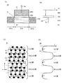
- FIGS. 10A and 10B are a cross-sectional view and a band diagram of a transistor according to one embodiment of the present invention, a diagram illustrating a crystal included in a metal oxide according to one embodiment of the present invention, and an energy at a lower end of a conduction band of the crystal.
- Figure. The figure explaining the layer structure of the crystal
- FIG. 10 is a perspective view of a transistor according to one embodiment of the present invention.
- FIGS. FIG. 6 are a cross-sectional view of a transistor according to one embodiment of the present invention and a crystal included in a metal oxide according to one embodiment of the present invention.
- FIGS. FIG. 6 is a cross-sectional view of a transistor according to one embodiment of the present invention.
- FIG. 10 is a perspective view of a transistor according to one embodiment of the present invention.
- FIG. 6 is a cross-sectional view of a transistor according to one embodiment of the present invention.
- FIG. 10 is a perspective view of a transistor according to one embodiment of the present invention.
- 4A and 4B are a cross-sectional view and a band diagram of a transistor according to one embodiment of the present invention, and a diagram illustrating a crystal included in a metal oxide according to one embodiment of the present invention.
- FIG. 4A and 4B are a top view and a cross-sectional view of a semiconductor device according to one embodiment of the present invention.
- FIG. 6 is a cross-sectional view of a semiconductor device according to one embodiment of the present invention.
- 4A and 4B are a top view and a cross-sectional view of a semiconductor device according to one embodiment of the present invention.
- 4A and 4B are a top view and a cross-sectional view of a semiconductor device according to one embodiment of the present invention.
- 4A and 4B are a top view and a cross-sectional view of a semiconductor device according to one embodiment of the present invention.
- 4A and 4B are a top view and a cross-sectional view of a semiconductor device according to one embodiment of the present invention.
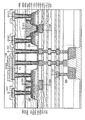
- FIG. 10 is a cross-sectional view illustrating a structure of a memory device according to one embodiment of the present invention.
- FIG. 10 is a cross-sectional view illustrating a structure of a memory device according to one embodiment of the present invention.
- 1A and 1B are a block diagram and a schematic diagram illustrating a structure example of a memory device according to one embodiment of the present invention.
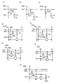
- FIG. 10 is a circuit diagram illustrating a structural example of a memory device according to one embodiment of the present invention.
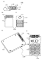
- FIG. 10 is a schematic view of a semiconductor device according to one embodiment of the present invention.
- FIG. 3 is a schematic diagram of a memory device according to one embodiment of the present invention.
- FIG. 14 illustrates an electronic device according to one embodiment of the present invention.
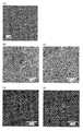
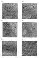
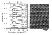
- the cross-sectional TEM image which concerns on the Example of this invention The cross-sectional TEM image which concerns on the Example of this invention.
- 4A and 4B illustrate temperature dependency of a V G- ID characteristic of a transistor.
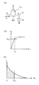
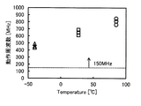
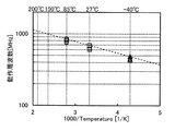
- the figure explaining the calculation method of an operating frequency The figure which shows the calculation result of an operating frequency.
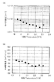
- 6A and 6B illustrate the carrier concentration and Hall mobility of an oxide semiconductor in one embodiment of the present invention.
- a top view also referred to as a “plan view”
- a perspective view a perspective view, and the like
- some components may be omitted in order to facilitate understanding of the invention.
- description of some hidden lines may be omitted.
- the ordinal numbers attached as the first and second are used for convenience and do not indicate the order of steps or the order of lamination. Therefore, for example, the description can be made by appropriately replacing “first” with “second” or “third”.
- the ordinal numbers described in this specification and the like may not match the ordinal numbers used to specify one embodiment of the present invention.
- X and Y are assumed to be objects (for example, devices, elements, circuits, wirings, electrodes, terminals, conductive films, layers, etc.).
- a transistor is an element having at least three terminals including a gate, a drain, and a source. And a region where a channel is formed between the drain (drain terminal, drain region or drain electrode) and the source (source terminal, source region or source electrode) (hereinafter also referred to as channel forming region). A current can flow between the source and the drain through the channel formation region.
- a channel formation region refers to a region through which a current mainly flows.
- the functions of the source and drain may be switched when transistors with different polarities are used or when the direction of current changes during circuit operation. Therefore, in this specification and the like, the terms “source” and “drain” may be used interchangeably.
- the channel length refers to, for example, a source in a region where a semiconductor (or a portion in which a current flows in the semiconductor when the transistor is on) and a gate electrode overlap with each other in a top view of the transistor or a channel formation region The distance between the (source region or source electrode) and the drain (drain region or drain electrode).
- the channel length is not necessarily the same in all regions. That is, the channel length of one transistor may not be fixed to one value. Therefore, in this specification and the like, the channel length is any one of values, the maximum value, the minimum value, or the average value in a channel formation region.
- the channel width is, for example, a channel length direction in a region where a semiconductor (or a portion where a current flows in the semiconductor when the transistor is on) and a gate electrode overlap with each other in a top view of the transistor Is the length of the channel forming region in the vertical direction.
- the channel width is not necessarily the same in all regions. That is, the channel width of one transistor may not be fixed to one value. Therefore, in this specification and the like, the channel width is any one of values, the maximum value, the minimum value, or the average value in a channel formation region.
- the channel width in a region where a channel is actually formed (hereinafter also referred to as an “effective channel width”) and the channel width shown in the top view of the transistor (Hereinafter also referred to as “apparent channel width”) may be different.
- the effective channel width when the gate electrode covers the side surface of the semiconductor, the effective channel width may be larger than the apparent channel width, and the influence may not be negligible.
- the ratio of a channel formation region formed on the side surface of the semiconductor may increase. In that case, the effective channel width is larger than the apparent channel width.
- channel width when simply referred to as channel width, it may indicate an apparent channel width.
- channel width in this specification and the like, in the case where the term “channel width” is simply used, it may denote an effective channel width. Note that the channel length, channel width, effective channel width, apparent channel width, and the like can be determined by analyzing a cross-sectional TEM image or the like.
- the impurity of a semiconductor means the thing other than the main component which comprises a semiconductor, for example.
- an element having a concentration of less than 0.1 atomic% can be said to be an impurity.
- the defect level density of the semiconductor may increase or the crystallinity may decrease.
- the impurity that changes the characteristics of the semiconductor include a Group 1 element, a Group 2 element, a Group 13 element, a Group 14 element, a Group 15 element, and an oxide semiconductor.
- water may also function as an impurity.
- oxygen vacancies may be formed, for example, by mixing impurities.
- impurities that change the characteristics of the semiconductor include group 1 elements, group 2 elements, group 13 elements, and group 15 elements excluding oxygen and hydrogen.
- silicon oxynitride has a higher oxygen content than nitrogen.
- silicon nitride oxide has a composition containing more nitrogen than oxygen.
- the term “insulator” can be referred to as an insulating film or an insulating layer.
- the term “conductor” can be restated as a conductive film or a conductive layer.
- the term “semiconductor” can be restated as a semiconductor film or a semiconductor layer.
- parallel means a state in which two straight lines are arranged at an angle of ⁇ 10 degrees to 10 degrees. Therefore, the case of -5 degrees or more and 5 degrees or less is also included.
- substantially parallel means a state in which two straight lines are arranged at an angle of ⁇ 30 degrees to 30 degrees.
- Vertical means a state in which two straight lines are arranged at an angle of 80 degrees to 100 degrees. Therefore, the case of 85 degrees or more and 95 degrees or less is also included.
- substantially vertical means a state in which two straight lines are arranged at an angle of 60 degrees or more and 120 degrees or less.
- the barrier film is a film having a function of suppressing permeation of impurities such as water and hydrogen and oxygen, and when the barrier film has conductivity, the conductive barrier film Sometimes called.
- a metal oxide is a metal oxide in a broad sense.
- Metal oxides are classified into oxide insulators, oxide conductors (including transparent oxide conductors), and oxide semiconductors (also referred to as oxide semiconductors or simply OS).
- oxide semiconductors also referred to as oxide semiconductors or simply OS.
- the metal oxide may be referred to as an oxide semiconductor. That is, in the case of describing as an OS transistor, it can be said to be a transistor including an oxide or an oxide semiconductor.
- normally-off means that when a potential is not applied to the gate or a ground potential is applied to the gate, a current per channel width of 1 ⁇ m flowing through the transistor is 1 ⁇ 10 ⁇ 20 at room temperature. A or lower, 1 ⁇ 10 ⁇ 18 A or lower at 85 ° C., or 1 ⁇ 10 ⁇ 16 A or lower at 125 ° C.
- FIG. 1A is a cross-sectional view in the channel length direction of the transistor 10 according to one embodiment of the present invention.
- the transistor 10 includes an oxide 230 disposed over a substrate (not shown), an insulator 250 disposed over the oxide 230, and the insulator 250. And a conductor 260 disposed on the top.
- the oxide 230 includes a region 234 that functions as a region where the channel of the transistor 10 is formed (hereinafter also referred to as a channel formation region) and a region 231 that functions as a source region or a drain region (a region 231a and a region 231b).
- the insulator 250 functions as a gate insulating film.
- the conductor 260 functions as a gate electrode.
- FIG. 1B is a model of a band diagram on an alternate long and short dash line indicated by X1-X2 in the transistor illustrated in FIG. In FIG. 1B, the k space is ignored. Note that FIG. 1B illustrates a state where no voltage is applied between the gate and the source.
- a solid line located on the conductor 260 indicates the position of the Fermi surface of the conductor 260.
- the solid line located on the insulator 250 indicates the position of the lower end of the conduction band of the insulator 250.
- the solid line located in the oxide 230 indicates the position of the lower end of the conduction band of the oxide 230.
- the transistor 10 can control the resistance of the channel portion by the potential applied to the gate. That is, conduction (transistor is on) and non-conduction (transistor is off) between the source and the drain can be controlled by the potential applied to the gate.
- a metal oxide functioning as a semiconductor (hereinafter also referred to as an oxide semiconductor) is preferably used for the oxide 230 including a channel formation region.
- An oxide semiconductor is preferable because a transistor has favorable switching characteristics and an extremely small off-state current can be obtained as compared with a semiconductor formed using silicon or the like.
- an oxide semiconductor can be formed by a sputtering method or the like, and thus can be used for a transistor included in a highly integrated semiconductor device.
- a transistor including an oxide semiconductor if an impurity and an oxygen vacancy exist in a channel formation region in the oxide semiconductor, electric characteristics are likely to fluctuate and reliability may be deteriorated.
- the channel formation region in the oxide semiconductor contains oxygen vacancies, the transistor tends to be normally on. Therefore, oxygen vacancies in the channel formation region are preferably reduced as much as possible.
- oxygen may be supplied to the oxide 230 through the insulator 250 or the like to fill oxygen vacancies. Accordingly, it is possible to provide a transistor that suppresses fluctuations in electrical characteristics, has stable electrical characteristics, and has improved reliability.
- a metal oxide having a low carrier density for the oxide 230.
- a metal oxide that is highly purified intrinsic or substantially highly purified intrinsic has few carrier generation sources, so that the carrier density can be lowered.
- a metal oxide that is highly purified intrinsic or substantially highly purified intrinsic has a low defect level density, and thus may have a low trap level density.
- the oxide 230 includes an In-M-Zn oxide (the element M is aluminum, gallium, yttrium, tin, copper, vanadium, beryllium, boron, titanium, iron, nickel, germanium, zirconium, molybdenum, lanthanum, cerium)
- a metal oxide such as one or more selected from neodymium, hafnium, tantalum, tungsten, magnesium, and the like may be used.
- the element M may be aluminum (Al), gallium (Ga), yttrium (Y), or tin (Sn).
- an In—Ga oxide or an In—Zn oxide may be used as the oxide 230.
- a conductive film functioning as a source electrode or a drain electrode may be provided so as to be in contact with the oxide 230.
- the low resistance region is partially formed between the oxide 230 and the conductive film or in the vicinity of the surface of the oxide 230. May be formed.
- impurities hydrogen, nitrogen, metal elements, etc.
- the carrier density may increase.
- at least part of the low resistance region is included in the region 231 functioning as a source region or a drain region.
- An oxide semiconductor (metal oxide) is classified into a single crystal oxide semiconductor and a non-single crystal oxide semiconductor.
- the non-single-crystal oxide semiconductor for example, a CAAC-OS (c-axis aligned crystal oxide semiconductor), a polycrystalline oxide semiconductor, an nc-OS (nanocrystalline oxide semiconductor), a pseudo-amorphous oxide semiconductor (a-like oxide semiconductor) OS: amorphous-like oxide semiconductor) and amorphous oxide semiconductor.
- a metal oxide that increases the on-state current of the transistor is preferably used.
- the mobility of the metal oxide used for the transistor is preferably increased.
- the crystal of the metal oxide preferably has a crystal structure in which the first layer and the second layer are included, and the first layer and the second layer are alternately stacked. .
- the first layer preferably has a wider band gap than the second layer. Note that in this specification and the like, the first layer has a wider band gap than the second layer, and the first layer may be expressed as having a wide gap.
- the second layer may be expressed as having a narrow gap when the band gap is narrower than that of the first layer. That is, the crystalline metal oxide preferably has a crystal in which the second layer having a narrow gap is sandwiched between the first layers having a wide gap.
- the first layer and the second layer included in the oxide 230 are each arranged substantially parallel to the channel length direction of the transistor 10. It can also be said that the extension directions of the first layer and the second layer of the oxide 230 are substantially parallel to the channel length direction of the transistor 10, respectively.
- each of the first layer and the second layer included in the oxide 230 is preferably disposed substantially parallel to the formation surface of the oxide 230.
- a crystalline metal oxide for example, a single crystal oxide semiconductor or CAAC-OS can be given.
- a crystalline metal oxide can improve carrier transmission. Accordingly, the mobility of the metal oxide is increased, the on-state current of the transistor including the metal oxide is increased, and the electrical characteristics of the transistor can be improved.
- the metal oxide is a metal oxide (also referred to as In-M-Zn oxide) including indium, the element M, zinc, and oxygen.
- the CAAC-OS has a c-axis orientation and a crystal structure in which a plurality of nanocrystals (crystal regions having a maximum diameter of less than 10 nm) are connected in the ab plane direction and have a strain.
- the strain refers to a portion where the orientation of the lattice arrangement changes between a region where the lattice arrangement is aligned and a region where another lattice arrangement is aligned in a region where a plurality of nanocrystals are connected.
- the nanocrystal is basically a hexagon, but is not necessarily a regular hexagon, and may be a non-regular hexagon.
- there may be a lattice arrangement such as a pentagon and a heptagon in the distortion.
- a clear crystal grain boundary also referred to as a grain boundary
- the formation of crystal grain boundaries is suppressed by the distortion of the lattice arrangement. This is because the CAAC-OS can tolerate distortion due to the fact that the arrangement of oxygen atoms is not dense in the ab plane direction and the bond distance between atoms changes due to substitution of metal elements. Because.
- the hexagonal shape of the crystalline metal oxide can be confirmed by an observation image of the metal oxide from a c-axis direction by a transmission electron microscope (TEM).
- TEM transmission electron microscope
- FIG. 1A An enlarged view of the region 51 of the oxide 230 illustrated in FIG. 1A is illustrated in FIG.
- the oxide 230 is an In-M-Zn oxide having a CAAC structure.
- the element M is Ga
- the c-axis direction of the In-M-Zn oxide having a CAAC structure is the vertical direction on the paper surface
- the ab surface direction is the horizontal direction on the paper surface. Normal direction.
- the oxide 230 may be a crystalline metal oxide.
- the composition formula is In (1 + ⁇ ) M (1- ⁇ ) O 3 (ZnO) m ( ⁇ is a real number of 0 or more and 1 or less, and m is 0.
- In-M-Zn oxide having a CAAC structure or a single crystal structure may be used.
- an In-M-Zn oxide having a CAAC structure includes a layer containing indium and oxygen (hereinafter referred to as an InO layer), and a layer including elements M, zinc, and oxygen (hereinafter referred to as an InO layer). , (M, Zn) O layer) and a layered crystal structure (also referred to as a layered crystal or a layered structure).
- the (M, Zn) O layer is a layer having an element M, zinc, and oxygen that is located between the InO layer and the InO layer adjacent to the InO layer in the c-axis direction. Refers to that.
- indium and the elements M and zinc can be substituted for each other, a part of indium may be contained in the (M, Zn) O layer. Further, a part of the element M or a part of zinc may be contained in the InO layer.
- the stack The formed structure may be called a crystal lattice.
- the first layer is an (M, Zn) O layer and the second layer is an InO layer.
- the crystal lattice may not be formed of two layers, and may be formed of three or more layers.
- the distance between the first layer and the second layer is preferably close to the distance between atoms constituting the crystal lattice.
- the distance between the first layer and the second layer is preferably 1 nm or less, more preferably 0.7 nm or less, and further preferably 0.5 nm or less. By doing so, the crystal lattice formed by the first layer and the second layer is structurally stable.
- the c-axis of the crystal included in the CAAC-OS is aligned in a direction normal to the formation surface of the oxide 230 or the film surface. Therefore, in the cross-sectional view of the transistor 10, the c-axis direction of the crystal included in the CAAC-OS is the vertical direction on the paper surface.
- the ab plane of the crystal included in the CAAC-OS is substantially parallel to the formation surface or the film surface of the oxide 230. That is, each of the InO layer and the (M, Zn) O layer is disposed substantially parallel to the surface on which the oxide 230 is formed. Therefore, the ab plane of the crystal included in the CAAC-OS is parallel to the left-right direction and the normal direction of the page.
- FIG. 1D an enlarged view of the region 52 at the lower end of the conduction band of the oxide 230 in the model of the band diagram shown in FIG. 1B is shown in FIG. In FIG. 1D, the k space is ignored. Note that the region 52 corresponds to the region 51 in the real space.
- the InO layer and the (M, Zn) O layer differ in the proportion of constituent elements contained in each layer. Therefore, the band gap is different between the InO layer and the (M, Zn) O layer.
- the InO layer and the (M, Zn) O layer have different electron affinity.
- the difference between the energy of the vacuum level and the energy Ec at the bottom of the conduction band is different between the InO layer and the (M, Zn) O layer.
- Gallium oxide is known to have a larger band gap than indium oxide. Therefore, when the element M is Ga, the band gap of the (M, Zn) O layer is estimated to be larger than the band gap of the InO layer. In addition, the electron affinity of the (M, Zn) O layer is estimated to be smaller than the electron affinity of the InO layer. In other words, in the InO layer, the difference between the energy at the vacuum level and the energy at the bottom of the conduction band is greater than the difference between the energy at the vacuum level and the energy at the bottom of the conduction band in the (M, Zn) O layer. Presumed.
- the lower end of the conduction band of the InO layer is located lower than the lower end of the conduction band of the (M, Zn) O layer.
- the (M, Zn) O layer may be expressed as having a wide gap.
- the InO layer may be expressed as having a narrow gap.
- the lower end of the conduction band of the InO layer and the lower end of the conduction band of the (M, Zn) O layer are the same as the InO layer. It is presumed that it continuously changes at the boundary with the (M, Zn) O layer. Therefore, as shown in FIG. 1D, the lower end of the conduction band of the oxide 230 is a level where the lower end of the conduction band of the InO layer and the lower end of the conduction band of the (M, Zn) O layer appear repeatedly. Guessed. Therefore, in the band diagram shown in FIG.
- the vicinity of the lower end of the conduction band of the (M, Zn) O layer is a convex portion, and the vicinity of the lower end of the conductive band of the InO layer is a concave portion.
- the InO layer and the (M, Zn) O layer are formed in the ab plane direction, the lower end of the conduction band in the ab plane direction is constant. Therefore, carriers are easily transmitted along the ab plane direction of the InO layer having the lower conduction band lower end.
- the carriers injected from the source are concentrated in the InO layer having the narrow gap sandwiched between the (M, Zn) O layers having the wide gap.
- the carrier transmission direction that is, the direction from the source to the drain, is the ab plane direction of the InO layer (the left-right direction of the page and the normal to the page).
- the main carrier transmission path is the InO layer. That is, when a carrier is excited in a crystalline metal oxide, the carrier is transmitted through the InO layer.
- carriers flow from the source to the drain through the channel formation region.
- carriers easily flow in the ab plane direction. Therefore, it is preferable to align the ab plane of the crystal of the In-M-Zn oxide with the carrier flow direction.
- the layered structure preferably extends to the region 231 included in the oxide 230. By doing so, carrier transmission between the region 231a and the region 231b through the channel formation region can be facilitated.
- CAAC-OS is a highly crystalline metal oxide.
- the lower end of the conduction band having a low trap state density due to the crystal grain boundary extends in the ab plane direction (this specification) Etc., it is also said that it has become a large level.) Therefore, it can be said that the decrease in electron mobility hardly occurs.
- the CAAC-OS can be said to be a metal oxide with few impurities and defects (such as oxygen vacancies). Therefore, the physical properties of the metal oxide including a CAAC-OS are stable. Therefore, a metal oxide including a CAAC-OS is resistant to heat and has high reliability.
- FIG. 2A illustrates a crystal structure of an In-M-Zn oxide having a CAAC structure.
- W_ (M, Zn) O indicates the thickness of the (M, Zn) O layer in the c-axis direction.
- W_ (M, Zn) O can also be referred to as the width of the convex portion at the lower end of the conduction band of the (M, Zn) O layer in the band diagram shown in FIG.
- W_InO indicates the thickness of the InO layer in the c-axis direction.
- W_InO can also be referred to as the width of the recess at the lower end of the conduction band of the InO layer in the band diagram shown in FIG.
- Wa_ (M, Zn) O shown in FIG. 2B is (M, Zn) O in the case where the temperature T is substantially the same as a reference temperature (for example, room temperature (RT)).
- Wa_InO shown in FIG. 2B indicates the thickness of the InO layer in the case where the temperature T is substantially the same as a reference temperature (for example, room temperature (RT)). The thickness in the c-axis direction is shown.
- Wb_ (M, Zn) O shown in FIG. 2C is (M, Zn) when the temperature T is higher than a reference temperature (for example, room temperature (RT)). The thickness of the O layer in the c-axis direction is shown, and Wb_InO shown in FIG.
- FIG. 2C is the InO in the case where the temperature T is higher than a reference temperature (for example, room temperature (RT)).
- a reference temperature for example, room temperature (RT)
- RT room temperature
- FIG. 2B and FIG. 2C the wavy line on the right side of the figure shows how the carrier transmits through the InO layer.
- the lattice vibration of atoms due to heat becomes smaller as the mass number of atoms increases.
- the metal oxide is an In—Ga—Zn oxide
- the atomic mass number is largest for In, then largest for Ga and Zn, and smallest for O. Therefore, Ga and Zn have larger lattice vibration due to heat than In.
- the vibration of atoms constituting the (Ga, Zn) O layer is increased as compared with the InO layer.
- the atomic bond between the InO layer and the (Ga, Zn) O layer is weaker than the atomic bond in the (Ga, Zn) O layer, the lattice vibration of Ga and Zn in the c-axis direction.
- Wb_ (Ga, Zn) is larger than Wa_ (Ga, Zn) O (see FIG. 2C).
- Wa_ (Ga, Zn) O the lattice constant in the c-axis direction of the layered crystal does not change with temperature
- the Wb_ (Ga, Zn) O layer becomes larger and Wb_InO becomes relatively smaller (see FIG. 2C). ). That is, the higher the temperature, the smaller the thickness of the InO layer in the c-axis direction.
- FIGS. 3A to 3C are diagrams schematically showing a band diagram in the crystal structure shown in FIG. 2A and a state in which carriers transmit the InO layer.
- the depth side of the paper corresponds to the source
- the front side of the paper corresponds to the drain
- the horizontal direction of the paper is the c-axis direction of the CAAC-OS.
- the wavy curved surface in the figure shows the lower end of the conduction band of the CAAC-OS.
- black circles indicate carriers (for example, electrons)
- dotted lines indicate schematic trajectories of the carriers.
- FIG. 3A shows a model having a temperature Ta that is substantially the same as a reference temperature (for example, room temperature (RT)), and Wa_ (M, Zn) O is the conduction of the (M, Zn) O layer.
- the width of the convex portion at the lower end of the band, and Wa_InO is the width of the concave portion at the lower end of the conduction band of the InO layer.
- 3B shows a model of a temperature Tb higher than a reference temperature (for example, room temperature (RT)), and Wb_ (M, Zn) O is the (M, Zn) O layer.
- Wb_InO is the width of the concave portion at the lower end of the conductive band of the InO layer.
- FIG. 3C shows a model of a temperature Tc higher than the temperature Tb.
- Wc_ (M, Zn) O is the width of the convex portion at the lower end of the conduction band of the (M, Zn) O layer
- Wc_InO is This is the width of the recess at the lower end of the conduction band of the InO layer.
- the main transmission path of the carrier is the InO layer.
- the thickness of the InO layer on the band diagram in the c-axis direction decreases, so that carriers are transmitted more planarly on the ab plane of the InO layer.
- the carrier is more linearly transmitted from the source to the drain, so that the mobility of the metal oxide is increased. Therefore, by using a metal oxide for the channel formation region of the transistor, the frequency characteristics are improved as the temperature is increased.
- carrier scattering so-called phonon scattering
- the drain electric field is increased and the carrier drift speed is increased. Improvement in drift velocity due to the shortening of the channel is suppressed by phonon scattering.
- phonon scattering is unlikely to occur, and thus it is difficult to suppress an improvement in drift speed due to a shortened channel.
- a crystalline metal oxide does not easily cause a short channel effect. Accordingly, miniaturization of a transistor in which a crystalline metal oxide is used for a channel formation region can be achieved.
- the channel length and the channel width of the transistor can be a region of 100 nm or less.
- MALT multi-atomic layer conduction
- Layers Transport transmission of carriers along the ab plane of a second layer having a narrow gap sandwiched between first layers having a wide gap.
- MALT multi-atomic layer conduction
- Layers Transport transmission of carriers along the ab plane of a second layer having a narrow gap sandwiched between first layers having a wide gap.
- the material from which MALT occurs is not limited to a semiconductor material in which a second layer having a narrow gap is sandwiched between first layers having a wide gap. Even if the first layer and the second layer are composed of the same element, the carrier may selectively or preferentially transmit one of the first layer and the second layer. .
- As a material for generating MALT for example, graphite having a laminated structure of graphene can be given.
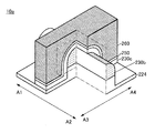
- FIG. 4 is a perspective view of the transistor 10a according to one embodiment of the present invention. In the perspective view of FIG. 4, some elements are omitted for the sake of clarity.
- FIGS. 5A and 5B are cross-sectional views of the transistor 10a according to one embodiment of the present invention.
- FIG. 5A is a cross-sectional view of the transistor 10a in the direction indicated by A1-A2 in FIG. 4, and is also a cross-sectional view of the transistor 10a in the channel length direction.
- FIG. 5B is a cross-sectional view of the transistor 10a in the direction indicated by A3-A4 in FIG. 4, and is also a cross-sectional view of the transistor 10a in the channel width direction.
- the transistor 10a includes an insulator 224 disposed over a substrate (not shown), an oxide 230b disposed over the insulator 224, and an oxide 230b. And an insulator 250 disposed on the oxide 230c, and a conductor 260 disposed on the insulator 250.
- the oxide 230c is provided so as to cover the upper surface and side surfaces of the oxide 230b.
- the insulator 250 is provided so as to cover the upper surface and the side surface of the oxide 230b with the oxide 230c interposed therebetween.
- the conductor 260 is provided so as to cover the upper surface and the side surface of the oxide 230b with the oxide 230c and the insulator 250 interposed therebetween.
- the insulator 250 functions as a gate insulating film. Further, the conductor 260 functions as a gate electrode.
- the oxide 230b includes a region 234 that functions as a channel formation region of the transistor 10a and a region 231 (a region 231a and a region 231b) that functions as a source region or a drain region. Further, the channel formation region may be formed in the oxide 230c.
- each of the first layer and the second layer included in the oxide 230b is approximately the surface over which the oxide 230b is formed (the upper surface of the insulator 224). It differs from the transistor 10 in that it is arranged vertically. It can also be said that the arrangement direction of the first layer and the second layer included in the oxide 230b of the transistor 10a is different from that of the transistor 10 in that it is parallel to the formation surface of the oxide 230b. However, also in the transistor 10 a, the first layer and the second layer included in the oxide 230 b are arranged substantially parallel to the channel length direction of the transistor 10. Note that the oxide 230b of the transistor 10a is the same as the oxide of the transistor 10 except that each of the first layer and the second layer is disposed substantially perpendicular to the formation surface of the oxide 230b. 230 has the same configuration.
- FIG. 5C An oxide 230b illustrated in FIG. 5C is an In-M-Zn oxide having a CAAC structure.
- the c-axis of the crystal included in the CAAC-OS is in a direction substantially parallel to the formation surface or film surface of the oxide 230b.
- the c-axis direction of the crystal included in the CAAC-OS is the horizontal direction on the paper.
- the ab plane of the crystal included in the CAAC-OS is substantially parallel to the normal direction to the formation surface or film surface of the oxide 230b. That is, the InO layer and the (M, Zn) O layer are each arranged substantially perpendicular to the surface on which the InO layer is formed. Therefore, in FIG. 5B, the ab plane of the crystal included in the CAAC-OS is parallel to the vertical direction of the paper surface and the normal direction of the paper surface.
- a structure body may be formed over the insulator 224, the oxide 230b may be formed using the side surface of the structure body as a formation surface, and the structure body may be removed.
- the side surface of the structure body is preferably substantially perpendicular to the upper surface of the insulator 224.
- the bottom surface of the conductor 260 in a region that does not overlap with the oxide 230b is preferably lower than the bottom surface of the oxide 230b when the bottom surface of the insulator 224 is used as a reference.
- the bottom surface of the first region that does not overlap with the oxide 230b also referred to as the bottom surface on the A3 side
- the conductor 260 face each other with the oxide 230b interposed therebetween. It is preferable that the position of the bottom surface of the second region (also referred to as the bottom surface on the A4 side) positioned lower than the bottom surface of the oxide 230b.
- the difference between the height of the bottom surface of the conductor 260 and the height of the bottom surface of the oxide 230b in a region where the oxide 230b and the conductor 260 do not overlap is 0 nm or more and 100 nm or less, preferably 3 nm or more. 50 nm or less, more preferably 5 nm or more and 20 nm or less.
- the conductor 260 functioning as a gate electrode covers the side surface and the upper surface of the oxide 230b in the channel formation region with the oxide 230c and the insulator 250 interposed therebetween.
- the electric field of the body 260 is easily applied to the entire region 234 of the oxide 230b.
- the electric field of the conductor 260 can also act on the bottom surface of the oxide 230b.
- a gate electric field can be applied to the region 234 of the oxide 230b from almost the entire periphery. Accordingly, since a channel can be formed in the entire region 234 of the oxide 230b, the on-state current of the transistor 10a can be increased and the frequency characteristics can be improved. In addition, by forming a channel in the entire region 234 of the oxide 230b in this manner, the off-state current of the transistor 10a can be reduced.
- the oxide 230b is preferably in the form of an elongated wire having a film thickness and a length in the channel width direction of about several nanometers to several tens of nanometers.
- Such an oxide 230b can be referred to as a nanowire.
- an elongated wire-like structure including the oxide 230b, the oxide 230c, the insulator 250, and the conductor 260 can be formed. it can.
- the transistor 10a can also be called a nanowire transistor because the electric field of the conductor 260 can be applied to the entire region 234 of the oxide 230b as described above.
- the metal oxide layer is rotated 90 degrees about the channel length direction as compared with the oxide 230 of the transistor 10.
- the transistor 10a by forming the transistor 10a into a nanowire shape, that is, by applying an electric field of the conductor 260 to the entire region 234 of the oxide 230b, the metal oxide layer is provided at any angle with respect to the conductor 260.
- the transistor 10a and the transistor 10 can be regarded as having the same characteristics.
- a metal oxide having a larger band gap than the oxide 230b may be used for the oxide 230c.
- a metal oxide having a small electron affinity may be used.
- a metal oxide having a small difference between the energy at the vacuum level and the energy at the lower end of the conduction band may be used. By doing so, the probability that carriers can move to the gate electrode and the gate insulating film can be reduced.
- the oxide 230c has a function of suppressing the diffusion of oxygen, it is possible to suppress the diffusion of the oxygen of the oxide 230b into the gate insulating film or the gate electrode.
- the oxide 230c has a function of suppressing diffusion of impurities, diffusion of impurities from the structure formed above the oxide 230c to the oxide 230b can be suppressed.
- the oxide 230c is illustrated as a single layer, but the oxide 230c may have a stacked structure.
- FIG. 6 shows a transistor 10b as a modification of the transistor 10a.
- 6A and 6B are cross-sectional views of the transistor 10b according to one embodiment of the present invention.
- FIG. 6A is a cross-sectional view of the transistor 10b in the channel length direction.
- FIG. 6B is a cross-sectional view of the transistor 10b in the channel width direction.
- transistor 10b the same reference numerals are given to structures having the same functions as the structures of the transistors 10 and 10a. Note that in this item, the material described in detail for the transistor 10 and the transistor 10a can be used as a constituent material of the transistor 10b.
- the transistor 10b is different from the transistor 10a in that the transistor 10b includes a conductor 205 which overlaps at least part of a region where the oxide 230b and the conductor 260 overlap with each other under the insulator 224. Note that in the transistor 10b, the oxide 230c which is provided in the transistor 10a is not provided.
- the conductor 260 may function as a first gate (also referred to as a top gate) electrode.
- the conductor 205 may function as a second gate (also referred to as a back gate) electrode.
- the threshold voltage (Vth) of the transistor 10b can be controlled by changing the potential applied to the conductor 205 independently of the potential applied to the conductor 260 without being linked.
- the Vth of the transistor 10b can be further increased and the off-state current can be reduced. Therefore, when a negative potential is applied to the conductor 205, the drain current when the potential applied to the conductor 260 is 0 V can be made smaller than when a negative potential is not applied.
- the conductor 205 is preferably provided larger than the channel formation region in the oxide 230b.
- the conductor 205 is preferably extended also in a region outside the end portion intersecting with the channel width direction of the oxide 230b. That is, it is preferable that the conductor 205 and the conductor 260 overlap with the insulator 224 outside the side surface in the channel width direction of the oxide 230.
- the oxide 230b can be formed by an electric field of the conductor 260 functioning as the first gate electrode and an electric field of the conductor 205 functioning as the second gate electrode.
- the channel forming region can be electrically surrounded.
- the electric field applied to the bottom surface of the oxide 230b can be further increased by the electric field of the conductor 205.
- a gate electric field can be applied to the region 234 of the oxide 230b from almost the entire periphery. Accordingly, since a channel can be formed in the entire region 234 of the oxide 230b, the on-state current of the transistor 10b can be increased and the frequency characteristics can be improved. In addition, by forming a channel in the entire region 234 of the oxide 230b in this manner, the off-state current of the transistor 10b can be reduced.
- the transistor 10b can be called a nanowire or a nanowire transistor because the electric field of the conductor 260 and the conductor 205 can be applied to the entire region 234 of the oxide 230b as in the transistor 10a.
- the structure of a transistor that electrically surrounds a channel formation region by the electric fields of the first gate electrode and the second gate electrode can be referred to as a surrounded channel (S-channel) structure.
- FIG. 7 is a perspective view of the transistor 10c according to one embodiment of the present invention. In the perspective view of FIG. 7, some elements are omitted for the sake of clarity.
- 8A and 8B are cross-sectional views of the transistor 10c according to one embodiment of the present invention.
- FIG. 8A is a cross-sectional view of the transistor 10c in the direction indicated by A1-A2 in FIG. 7, and is also a cross-sectional view of the transistor 10c in the channel length direction.
- FIG. 8B is a cross-sectional view of the transistor 10c in the direction indicated by A3-A4 in FIG. 7, and is also a cross-sectional view of the transistor 10c in the channel width direction.
- transistor 10c structures having the same functions as those of the transistors 10, 10a, and 10b are denoted by the same reference numerals. Note that in this item, the material described in detail for the transistor 10, the transistor 10a, and the transistor 10b can be used as a constituent material of the transistor 10c.
- the transistor 10c is different from the transistor 10a in that an oxide 230a is provided between the insulator 224 and the oxide 230b. That is, the oxide 230 includes the oxide 230a over the insulator 224, the oxide 230b over the oxide 230a, and the oxide 230c over the oxide 230b.
- the oxide 230a is preferably an oxide similar to the oxide 230c.
- a metal oxide having a larger band gap than the oxide 230b may be used for the oxide 230a.
- a metal oxide having a small electron affinity may be used.
- a metal oxide having a small difference between the energy at the vacuum level and the energy at the lower end of the conduction band may be used. In this manner, the probability that carriers can move to the insulator 224 can be reduced.
- the oxide 230a preferably has an upper surface in contact with the oxide 230b and a side surface in contact with the oxide 230c as illustrated in FIG. 8B.
- the oxide 230b can be covered with the oxide 230a and the oxide 230c.
- the oxide 230 b can be isolated from the insulator 224 and the insulator 250 in the region 234. Accordingly, in the oxide 230b, the probability that carriers can move to the outside can be reduced, and the diffusion of oxygen to the outside and the diffusion of impurities from the outside can be suppressed.
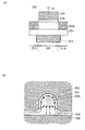
- FIG. 9 is a perspective view of a transistor 10d according to one embodiment of the present invention.
- 10A and 10B are cross-sectional views of the transistor 10d according to one embodiment of the present invention.
- FIG. 10A is a cross-sectional view of the transistor 10d in the direction indicated by A1-A2 in FIG. 9, and is also a cross-sectional view of the transistor 10d in the channel length direction.
- FIG. 10B is a cross-sectional view of the transistor 10d in the direction indicated by A3-A4 in FIG. 9, and is also a cross-sectional view of the transistor 10d in the channel width direction.
- the same reference numerals are given to structures having the same functions as the structures of the transistor 10, the transistor 10a, the transistor 10b, and the transistor 10c. Note that in this item, the material described in detail for the transistor 10, the transistor 10a, the transistor 10b, and the transistor 10c can be used as a constituent material of the transistor 10d.
- the transistor 10d includes an insulator 224 disposed over a substrate (not shown), an oxide 230b disposed over the insulator 224, and an oxide 230b. And an insulator 250 disposed on the oxide 230c, and a conductor 260 disposed on the insulator 250.
- the oxide 230c is provided so as to cover the top surface and the side surface of the oxide 230b in the channel width direction of the transistor 10d.
- the insulator 250 is provided so as to cover the upper surface and the side surface of the oxide 230b with the oxide 230c interposed therebetween.
- the conductor 260 is provided so as to cover the upper surface and the side surface of the oxide 230b with the oxide 230c and the insulator 250 interposed therebetween.
- the insulator 250 functions as a gate insulating film. Further, the conductor 260 functions as a gate electrode.
- the oxide 230b includes a region 234 functioning as a channel formation region of the transistor 10d and a region 231 (region 231a and region 231b) functioning as a source region or a drain region. Further, the channel formation region may be formed in the oxide 230c.
- the bottom surface of the conductor 260 in a region that does not overlap with the oxide 230b is preferably lower than the bottom surface of the oxide 230b when the bottom surface of the insulator 224 is used as a reference.
- the conductor 260 functioning as a gate electrode covers the side surface and the upper surface of the oxide 230b in the channel formation region with the oxide 230c and the insulator 250 interposed therebetween, whereby the electric field of the conductor 260 is applied to the region of the oxide 230b. It becomes easy to make it act on 234 whole. Thus, the on-state current of the transistor 10d can be increased and the frequency characteristics can be improved.
- the difference between the height of the bottom surface of the conductor 260 and the height of the bottom surface of the oxide 230b in a region where the oxide 230b and the conductor 260 do not overlap each other is 0 nm to 100 nm, preferably 3 nm to 50 nm. More preferably, it is 5 nm or more and 20 nm or less.
- At least one of the oxide 230b and the oxide 230c is preferably a crystalline metal oxide. Specifically, at least one of the oxide 230b and the oxide 230c is preferably a single crystal oxide semiconductor or a CAAC-OS.
- the oxide 230b is illustrated as a single layer, a stacked structure may be employed.
- the oxide 230b has a two-layer structure, the lower layer of the oxide 230b is in contact with the insulator 224, and the upper layer of the oxide 230b is in contact with the oxide 230c.
- diffusion of impurities from the structure formed below the lower layer of the oxide 230b to the oxide 230b can be suppressed.
- FIG. 10B An enlarged view of the region 54 of the oxide 230b shown in FIG. 10B is shown in FIG. A region 55 of the oxide 230c illustrated in FIG. 10B is illustrated in FIG. Note that the oxide 230b and the oxide 230c are In-M-Zn oxides having a CAAC structure.
- the c-axis of the crystal included in the oxide 230b is aligned in a direction normal to the formation surface of the oxide 230b or the film surface, and the ab plane is The surface of the oxide 230b is substantially parallel to the surface or film surface. Therefore, in the region 54 of the oxide 230b illustrated in FIG. 10D, the c-axis direction of the crystal included in the oxide 230b is the vertical direction of the drawing. In addition, the ab plane of the crystal included in the oxide 230b is parallel to the horizontal direction of the paper surface and the normal direction of the paper surface.
- the c-axis of the crystal included in the CAAC-OS is oriented in a direction substantially perpendicular to the CAAC-OS formation surface, and the ab plane is substantially parallel to the CAAC-OS formation surface. Accordingly, in the case where a crystalline metal oxide is used for the oxide 230c, the orientation of the c-axis of the crystal included in the oxide 230c in the region 55 of the oxide 230c illustrated in FIG. The horizontal direction of the paper. In addition, the ab plane of the crystal included in the oxide 230c is parallel to the vertical direction of the page and the normal direction of the page.
- the c-axis direction of the crystal included in the oxide 230b is different from the c-axis direction of the crystal included in the oxide 230c on the dashed-dotted line illustrated in X5-X6 in FIG.
- Carrier transmission model 2 Here, carrier transmission in a transistor in which the oxide 230b and the oxide 230c are stacked is described using the carrier transmission model described above.
- FIG. 10C illustrates a band diagram model on the alternate long and short dash line indicated by X5-X6 in the transistor 10d illustrated in FIGS. 10A and 10B. Note that FIG. 10C illustrates a state in which a positive potential is applied to the gate electrode. FIG. 10C illustrates an example in which the oxides 230b and 230c are metal oxides having the same energy at the bottom of the conduction band.
- the ab plane of the crystal included in the oxide 230b is substantially parallel to the substrate surface inside the oxide 230b. Therefore, the energy at the lower end of the conduction band of the oxide 230b on the alternate long and short dash line indicated by X5-X6 is constant. In addition, an electric field is generated in the ab plane direction of the crystal included in the oxide 230b inside the oxide 230b. In addition, the electric field applied to the surface of the oxide 230b is smaller in the oxide 230b. Therefore, the bending of the lower end of the conduction band inside the oxide 230b is small.
- the oxide 230c an electric field is generated in the c-axis direction of the crystal of the oxide 230c.
- the electric field generated by the oxide 230c is larger than the electric field applied to the inside of the oxide 230b. Therefore, the bending of the band in the oxide 230c is large (see the dotted line in FIG. 10C).
- the ab plane of the crystal included in the oxide 230c is substantially perpendicular to the substrate plane. Therefore, as shown in FIG.
- the lower end of the conduction band of the oxide 230c is the lower end of the conduction band derived from the InO layer and the conduction band derived from the (M, Zn) O layer on the alternate long and short dash line indicated by X5-X6. The lower end appears alternately.
- the carriers injected from the source are concentrated on the InO layer of the oxide 230c having the lower conduction band lower end. Further, the carriers are transmitted between the source and the drain, that is, transmitted in the ab plane direction.
- the main carrier transmission path is the InO layer of the oxide 230b or the InO layer of the oxide 230c on the dashed-dotted line indicated by X5-X6.
- the carriers are too concentrated, repulsion due to Coulomb force occurs between carriers, and carrier transmission is suppressed.
- the metal oxide having a layered crystal as shown in FIG. 10C, since there are a plurality of InO layers which are main carrier transmission paths, they are dispersed in an InO layer where a plurality of carriers exist. Therefore, the concentration of carriers is alleviated, and repulsion due to Coulomb force hardly occurs between carriers, and carrier transmission is not suppressed.
- a metal oxide having a larger band gap than the oxide 230b may be used for the oxide 230c.
- a metal oxide having a small electron affinity may be used.
- a metal oxide having a small difference between the energy at the vacuum level and the energy at the lower end of the conduction band may be used. By doing so, the probability that carriers can move to the gate electrode and the gate insulating film can be reduced.
- the oxide 230c is illustrated as a single layer, but may have a stacked structure.
- the lower layer of the oxide 230c is in contact with the oxide 230b and the upper layer of the oxide 230c is in contact with the insulator 250.
- a metal oxide having the same composition as that of the oxide 230b is used for a lower layer of the oxide 230c, and a metal oxide having a band gap larger than that of the oxide 230b is preferably used for an upper layer of the oxide 230c.
- the upper layer of the oxide 230c has a function of suppressing oxygen diffusion
- oxygen in the lower layer of the oxide 230b and the oxide 230c can suppress diffusion into the gate insulating film or the gate electrode.
- impurities from the structure formed above the upper layer of the oxide 230c to the lower layer of the oxide 230c and the oxide 230b Diffusion can be suppressed.
- a semiconductor device including a transistor with high on-state current can be provided.
- a semiconductor device including a transistor having high frequency characteristics can be provided.
- a semiconductor device including a transistor with low off-state current can be provided.
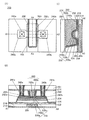
- 11A to 11C are a top view and a cross-sectional view of the transistor 200 and the periphery of the transistor 200 according to one embodiment of the present invention.
- FIG. 11A is a top view of a semiconductor device including a transistor 200.
- FIG. 11B and 11C are cross-sectional views of the semiconductor device.
- FIG. 11B is a cross-sectional view taken along dashed-dotted line A1-A2 in FIG. 11A and also a cross-sectional view in the channel length direction of the transistor 200.
- FIG. 11C is a cross-sectional view taken along dashed-dotted line A3-A4 in FIG. 11A and is a cross-sectional view in the channel width direction of the transistor 200. Note that in the top view of FIG. 11A, some elements are omitted for clarity.
- the semiconductor device of one embodiment of the present invention includes the transistor 200, the insulator 214 functioning as an interlayer film, the insulator 280, the insulator 274, and the insulator 281.
- a conductor 240 (a conductor 240a and a conductor 240b) which is electrically connected to the transistor 200 and functions as a plug is provided.
- an insulator 241 (the insulator 241a and the insulator 241b) is provided in contact with a side surface of the conductor 240 functioning as a plug.
- an insulator 241 is provided in contact with the sidewalls of the openings of the insulator 254, the insulator 280, the insulator 274, and the insulator 281 and a first conductor of the conductor 240 is provided in contact with the side surface thereof. Further, a second conductor of the conductor 240 is provided inside.
- the height of the upper surface of the conductor 240 and the height of the upper surface of the insulator 281 can be approximately the same.
- the conductor 240 may be provided as a single layer or a stacked structure of three or more layers. When a structure has a laminated structure, an ordinal number may be given in the order of formation to be distinguished.
- the transistor 200 includes an insulator 216 disposed over a substrate (not shown), a conductor 205 disposed to be embedded in the insulator 216, and the insulator 216. And an insulator 222 disposed on the conductor 205, an insulator 224 disposed on the insulator 222, and an oxide 230 (oxide 230a, oxide 230b, And oxide 230c), insulator 250 disposed on oxide 230, conductor 260 (conductor 260a and conductor 260b) disposed on insulator 250, and top surface of oxide 230b.
- Conductor 242a and conductor 242b in contact with part, part of the top surface of insulator 222, side surface of insulator 224, side surface of oxide 230a, side surface of oxide 230b, side of conductor 242a Has an upper surface of the conductor 242a, the side surface of the conductor 242b, and an insulator 254 which is arranged in contact with the upper surface of the conductor 242b, a.
- the conductor 260 functions as a gate electrode of the transistor, and the conductor 242a and the conductor 242b function as a source electrode or a drain electrode, respectively.
- a conductor 260 functioning as a gate electrode is formed in a self-aligning manner so as to fill an opening formed in the insulator 280 or the like. By forming the conductor 260 in this manner, the conductor 260 can be reliably arranged in the region between the conductors 242a and 242b without being aligned.
- the conductor 260 has the conductor 260a and the conductor 260b arrange
- the conductor 260a is preferably arranged so as to wrap around the bottom and side surfaces of the conductor 260b.
- the upper surface of the conductor 260 substantially matches the upper surface of the insulator 250 and the upper surface of the oxide 230c.
- the conductor 260 is illustrated as a two-layer structure in the transistor 200, the present invention is not limited to this.
- the conductor 260 may have a single layer structure or a stacked structure of three or more layers.
- the insulator 222, the insulator 254, and the insulator 274 preferably have a function of suppressing diffusion of hydrogen (for example, at least one of a hydrogen atom and a hydrogen molecule).
- the insulator 222, the insulator 254, and the insulator 274 preferably have a function of suppressing diffusion of oxygen (for example, at least one of oxygen atoms and oxygen molecules).
- the insulator 222, the insulator 254, and the insulator 274 preferably each have lower permeability of one or both of hydrogen and oxygen than the insulator 224.
- the insulator 222, the insulator 254, and the insulator 274 preferably each have lower permeability of one or both of hydrogen and oxygen than the insulator 250.
- the insulator 222, the insulator 254, and the insulator 274 preferably each have lower permeability to one or both of hydrogen and oxygen than the insulator 280.
- the oxide 230 includes an oxide 230a disposed over the insulator 224, an oxide 230b disposed over the oxide 230a, and an oxide 230b, and at least a portion of the oxide 230b. And an oxide 230c in contact with the upper surface. As illustrated in FIG. 11C, the oxide 230c is preferably provided so as to cover the top surface and the side surface of the oxide 230b in the channel width direction of the transistor 200.
- the oxide 230, the insulator 250, the conductor 260, the insulator 224, and the conductor 205 correspond to the structures of the transistor 10 or the transistors 10a to 10d described in the above embodiment.
- a structure in which a layer where a channel is formed (hereinafter also referred to as a channel formation region) and three layers of an oxide 230a, an oxide 230b, and an oxide 230c are stacked is shown.
- the present invention is not limited to this.
- a structure in which a single layer of the oxide 230b, a two-layer structure of the oxide 230a and the oxide 230b, a two-layer structure of the oxide 230b and the oxide 230c, or a stacked structure of four or more layers may be employed.
- each of the oxide 230a, the oxide 230b, and the oxide 230c may have a stacked structure of two or more layers.
- the oxide 230c has a stacked structure including a first oxide and a second oxide over the first oxide
- the first oxide has a composition similar to that of the oxide 230b.
- the second oxide may have a composition similar to that of the oxide 230a.
- a metal oxide that functions as a semiconductor (hereinafter also referred to as an oxide semiconductor) is used for the oxide 230 (the oxide 230a, the oxide 230b, and the oxide 230c) including the channel formation region. Is preferred.
- the transistor 200 using an oxide semiconductor in a channel formation region has extremely small leakage current (off-state current) in a non-conduction state, a semiconductor device with low power consumption can be provided.
- An oxide semiconductor can be formed by a sputtering method or the like, and thus can be used for the transistor 200 included in a highly integrated semiconductor device.
- the oxide 230 includes an In-M-Zn oxide (the element M is aluminum, gallium, yttrium, tin, copper, vanadium, beryllium, boron, titanium, iron, nickel, germanium, zirconium, molybdenum, lanthanum, cerium)
- a metal oxide such as one or more selected from neodymium, hafnium, tantalum, tungsten, magnesium, and the like may be used.
- the element M may be aluminum, gallium, yttrium, or tin.
- an In—Ga oxide, an In—Zn oxide, or a Ga—Zn oxide may be used as the oxide 230.
- the oxide 230 corresponds to the oxide 230 described in the above embodiment. Therefore, a crystalline metal oxide is preferably used for the oxide 230 including a channel formation region of the transistor 200.
- the crystal of the metal oxide preferably has a crystal structure in which the first layer and the second layer are included, and the first layer and the second layer are alternately stacked. .
- the first layer preferably has a wider band gap than the second layer.
- a crystalline metal oxide for example, a single crystal oxide semiconductor or a CAAC-OS can be given.
- a crystalline metal oxide can improve carrier transmission. Accordingly, the mobility of the metal oxide is increased, the on-state current of the transistor including the metal oxide is increased, and the electrical characteristics of the transistor can be improved.
- FIG. 11C is a cross-sectional view of the transistor 200 in the channel width direction, similarly to FIG. 10B. Therefore, the region corresponding to the region 54 of the oxide 230b illustrated in FIG. 10B has the crystal structure illustrated in FIG. 10D and corresponds to the region 55 of the oxide 230c illustrated in FIG. The region has a crystal structure illustrated in FIG. Therefore, since the transistor 200 satisfies the model of the schematic band diagram illustrated in FIG. 10C, it is possible to prevent suppression of carrier transmission.
- a physical distance between the region located in the vicinity of the interface between the oxide 230c and the insulator 274 and the channel formation region of the oxide 230 be separated.
- the trap state density may be high. Therefore, the physical distance between the region located in the vicinity of the interface between the oxide 230c and the insulator 274 and the channel formation region of the oxide 230 is increased, so that variation in electrical characteristics of the transistor 200 is suppressed and reliability is improved. Can be improved.
- a transistor including an oxide semiconductor if an impurity and an oxygen vacancy exist in a channel formation region in the oxide semiconductor, electric characteristics are likely to fluctuate and reliability may be deteriorated.
- the channel formation region in the oxide semiconductor contains oxygen vacancies, the transistor tends to be normally on. Therefore, oxygen vacancies in the channel formation region are preferably reduced as much as possible.
- oxygen may be supplied to the oxide 230 through the oxide 230c, the insulator 250, or the like to fill oxygen vacancies. Accordingly, it is possible to provide a transistor that suppresses fluctuations in electrical characteristics, has stable electrical characteristics, and has improved reliability.
- an element included in the conductor 242 (the conductor 242a and the conductor 242b) that is provided in contact with the oxide 230 and functions as a source electrode or a drain electrode has a function of absorbing oxygen in the oxide 230.
- a low resistance region is partially formed between the oxide 230 and the conductor 242 or in the vicinity of the surface of the oxide 230.
- impurities hydrogen, nitrogen, metal elements, etc.
- the carrier density may increase.
- FIG. 12A is an enlarged view of a part of the region of the transistor 200 illustrated in FIG.
- a conductor 242 is provided so as to be in contact with the oxide 230, and a region 243 (as a low resistance region is provided near and in the vicinity of the interface of the oxide 230 with the conductor 242.
- a region 243a and a region 243b) may be formed.
- the oxide 230 includes a region 234 that functions as a channel formation region of the transistor 200 and a region 231 (a region 231a and a region 231b) that includes at least part of the region 243 and functions as a source region or a drain region. Note that in the subsequent drawings, a similar region 243 may be formed even when the region 243 is not shown in an enlarged view or the like.
- the region 243a and the region 243b are provided so as to diffuse in the depth direction in the vicinity of the conductor 242 of the oxide 230b, the present invention is not limited thereto.
- the region 243a and the region 243b may be formed as appropriate depending on required electrical characteristics of the transistor.
- the concentration of the element detected in each region is not limited to a stepwise change for each region, but may continuously change (also referred to as gradation) within each region.
- the insulator 254 includes the conductors 242a and 242b other than the top surfaces of the conductors 242a and 242b and the side surfaces of the conductors 242a and 242b that face each other.
- the side surface, the side surfaces of the oxide 230a and the oxide 230b, the side surface of the insulator 224, and part of the top surface of the insulator 222 are preferably in contact with each other.
- the insulator 280 is separated from the insulator 224, the oxide 230a, and the oxide 230b by the insulator 254. Therefore, impurities such as hydrogen contained in the insulator 280 and the like can be prevented from entering the insulator 224, the oxide 230a, and the oxide 230b.
- the insulator 274 is in contact with the upper surfaces of the conductor 260, the insulator 250, and the oxide 230c.
- the transistor 200 which is one embodiment of the present invention has a structure in which the insulator 274 and the insulator 250 are in contact with each other as illustrated in FIG. With such a structure, impurities such as hydrogen contained in the insulator 281 and the like can be prevented from entering the insulator 250. Accordingly, adverse effects on the electrical characteristics of the transistor and the reliability of the transistor can be suppressed.
- the height of the bottom surface of the conductor 260 in a region overlapping with the region 234 with respect to the bottom surface of the insulator 224 is higher than the top surface of each of the conductors 242a and 242b. May be lower.
- the difference between the height of the bottom surface of the conductor 260 in the region overlapping with the region 234 and the height of each upper surface of the conductors 242a and 242b is 0 nm to 30 nm, or 0 nm to 15 nm.
- FIG. 12B is an enlarged view of a part of the region of the transistor 200 illustrated in FIG. Similar to the previous embodiment, the height of the bottom surface of the conductor 260 in the region where the conductor 260 and the oxide 230b do not overlap with each other with respect to the bottom surface of the insulator 222 in the channel width direction of the transistor 200. Is preferably lower than the height of the bottom surface of the oxide 230b.
- the conductor 260 functioning as a gate electrode covers the side surface and the upper surface of the oxide 230b in the channel formation region with the oxide 230c and the insulator 250 interposed therebetween, whereby the electric field of the conductor 260 is applied to the region of the oxide 230b. It becomes easy to make it act on 234 whole.
- T2 is 0 nm or more and 100 nm. In the following, it is preferably 3 nm to 50 nm, more preferably 5 nm to 20 nm.
- the oxide 230c in a region which does not overlap with the oxide 230b, the oxide 230a, and the insulator 224 in the channel width direction of the transistor 200 It is preferable to contact.
- oxygen contained in the oxide 230 c can be prevented from diffusing outside the transistor 200 through the insulator 224.
- the oxide 230b and oxygen contained in the oxide 230a can be prevented from diffusing outside the transistor 200 through the insulator 224.
- the area of the insulator 224 is reduced, the amount of oxygen taken into the insulator 224 is reduced, and a reduction in the amount of oxygen supplied to the oxide 230 can be suppressed.
- oxygen contained in the oxide 230c can be efficiently supplied to the oxide 230b and the oxide 230a, and reduction in resistance of the oxide 230 in the region 234 can be suppressed. Therefore, variation in electrical characteristics of the transistor can be suppressed, stable electrical characteristics can be obtained, and reliability can be improved.
- the structure can be formed by removing the oxide 230b and the insulator 224 in a region which does not overlap with the oxide 230a.
- the bottom surface of the insulator 222 is used as a reference in the channel width direction of the transistor 200 as illustrated in FIG.
- the height of the bottom surface of the conductor 260 in a region where the oxide 230a and the oxide 230b do not overlap with the conductor 260 is likely to be lower than the height of the bottom surface of the oxide 230b. Accordingly, the on-state current of the transistor 200 can be increased and the frequency characteristics can be improved.
- a semiconductor device including a transistor with high on-state current can be provided.
- a semiconductor device including a transistor having high frequency characteristics can be provided.
- a semiconductor device including a transistor with low off-state current can be provided.
- the conductor 205 is disposed so as to overlap with the oxide 230 and the conductor 260.
- the conductor 205 is preferably provided so as to be embedded in the insulator 214 and the insulator 216.
- the flatness of the upper surface of the conductor 205 is preferably improved.
- the average surface roughness (Ra) of the upper surface of the conductor 205 may be 1 nm or less, preferably 0.5 nm or less, more preferably 0.3 nm or less. Accordingly, the flatness of the insulator 224 formed over the conductor 205 can be improved, and the crystallinity of the oxide 230a, the oxide 230b, and the oxide 230c can be improved.
- the conductor 260 may function as a first gate (also referred to as a top gate) electrode.
- the conductor 205 may function as a second gate (also referred to as a back gate) electrode.
- the threshold voltage (Vth) of the transistor 200 can be controlled by changing the potential applied to the conductor 205 independently of the potential applied to the conductor 260 without being linked.
- the Vth of the transistor 200 can be increased and the off-state current can be reduced. Therefore, when a negative potential is applied to the conductor 205, the drain current when the potential applied to the conductor 260 is 0 V can be made smaller than when a negative potential is not applied.
- the conductor 205 is preferably provided larger than the channel formation region in the oxide 230 as illustrated in FIG.
- the conductor 205 is preferably extended also in a region outside the end portion that intersects the channel width direction of the oxide 230. That is, it is preferable that the conductor 205 and the conductor 260 overlap with each other with an insulator outside the side surface in the channel width direction of the oxide 230.
- the channel formation region of the oxide 230 is electrically surrounded by the electric field of the conductor 260 functioning as the first gate electrode and the electric field of the conductor 205 functioning as the second gate electrode. Can do.
- the conductor 205 is extended to function as wiring.
- the present invention is not limited to this, and a conductor functioning as a wiring may be provided below the conductor 205.
- One conductor 205 is not necessarily provided for each transistor.
- the conductor 205 may be shared by a plurality of transistors.
- the conductor 205 is preferably formed using a conductive material mainly containing tungsten, copper, or aluminum. Note that although the conductor 205 is illustrated as a single layer, it may have a stacked structure, for example, a stack of titanium, titanium nitride, and the above conductive material.
- a function of suppressing diffusion of impurities such as a hydrogen atom, a hydrogen molecule, a water molecule, a nitrogen atom, a nitrogen molecule, a nitrogen oxide molecule (N 2 O, NO, NO 2, and the like) or a copper atom under the conductor 205
- a conductor may be provided (it is difficult for the impurities to pass through).
- the function of suppressing diffusion of impurities or oxygen is a function of suppressing diffusion of any one or all of the impurities and oxygen.
- the conductivity of the conductor 205 can be suppressed from being reduced.
- the conductor having a function of suppressing oxygen diffusion for example, tantalum, tantalum nitride, ruthenium, or ruthenium oxide is preferably used. Therefore, the conductive material may be a single layer or a stacked layer as the conductor below the conductor 205.
- the conductor 205 is formed by a sputtering method, a chemical vapor deposition (CVD) method, a molecular beam epitaxy (MBE) method, a pulsed laser deposition (PLD) method, Alternatively, it can be performed by using an atomic layer deposition (ALD) method or the like.
- CVD chemical vapor deposition
- MBE molecular beam epitaxy
- PLD pulsed laser deposition
- ALD atomic layer deposition
- the conductor 205 for example, a stacked film in which a conductive film is formed in the order of tantalum nitride, titanium nitride, and tungsten can be used.
- the insulator 214 provided over a substrate preferably functions as a barrier insulating film that suppresses diffusion of impurities such as water and hydrogen from the substrate side to the transistor 200. Therefore, the insulator 214 has a function of suppressing diffusion of impurities such as hydrogen atoms, hydrogen molecules, water molecules, nitrogen atoms, nitrogen molecules, nitric oxide molecules (N 2 O, NO, NO 2, and the like) and copper atoms. (It is difficult for the impurities to permeate.) It is preferable to use an insulating material. Alternatively, it is preferable to use an insulating material having a function of suppressing diffusion of oxygen (for example, at least one of an oxygen atom and an oxygen molecule) (the oxygen hardly transmits).
- the insulator 214 it is preferable to use aluminum oxide, silicon nitride, or the like as the insulator 214.
- impurities such as water and hydrogen can be prevented from diffusing from the substrate side to the transistor 200 side with respect to the insulator 214.
- diffusion of oxygen contained in the insulator 224 and the like to the substrate side with respect to the insulator 214 can be suppressed.
- the insulator 214 can be formed by a sputtering method, a CVD method, an MBE method, a PLD method, an ALD method, or the like.
- a sputtering method for example, aluminum oxide formed by a sputtering method can be used.
- the insulator 216 disposed on the insulator 214 functions as an interlayer film.
- the insulator 280 and the insulator 281 disposed over the insulator 254 also function as an interlayer film.
- the insulator 216, the insulator 280, and the insulator 281 which function as interlayer films preferably have a lower dielectric constant than the insulator 214.
- silicon oxide, silicon oxynitride, silicon nitride oxide, silicon nitride, silicon oxide added with fluorine, silicon oxide added with carbon, carbon, and nitrogen were added.
- Silicon oxide, silicon oxide having holes, or the like may be used as appropriate.
- the insulator 216 may have a laminated structure.
- an insulator similar to the insulator 214 may be provided at least in a portion in contact with the side surface of the conductor 205.
- the conductor 205 can be prevented from being oxidized by oxygen contained in the insulator 216.
- the conductor 205 can suppress absorption of oxygen contained in the insulator 216.
- the insulator 216 can be formed by a sputtering method, a CVD method, an MBE method, a PLD method, an ALD method, or the like.
- silicon oxynitride formed by a CVD method can be used as the insulator 216.
- the insulator 222 and the insulator 224 have a function as a gate insulator.
- the insulator 224 in contact with the oxide 230 desorbs oxygen by heating.
- oxygen released by heating may be referred to as excess oxygen.
- the insulator 224 may be formed using silicon oxide, silicon oxynitride, or the like as appropriate.
- an oxide film from which part of oxygen is released by heating is preferably used as the insulator 224.
- the oxide film that desorbs oxygen by heating means that the amount of desorbed oxygen converted to oxygen atoms is 1.0 ⁇ 10 18 atoms / cm 3 or more, preferably 1 in TDS (Thermal Desorption Spectroscopy) analysis.
- the oxide film has a thickness of 0.0 ⁇ 10 19 atoms / cm 3 or more, more preferably 2.0 ⁇ 10 19 atoms / cm 3 or more, or 3.0 ⁇ 10 20 atoms / cm 3 or more.
- the surface temperature of the film at the time of TDS analysis is preferably in the range of 100 ° C. to 700 ° C., or 100 ° C. to 400 ° C.
- the insulator 224 can be formed by a sputtering method, a CVD method, an MBE method, a PLD method, an ALD method, or the like.
- silicon oxynitride formed by a CVD method can be used as the insulator 224.
- the insulator 224 has an island shape; however, this embodiment is not limited thereto.
- the insulator 224 can cover the entire surface of the insulator 222.
- the insulator 222 preferably functions as a barrier insulating film that suppresses diffusion of impurities such as water and hydrogen from the substrate side to the transistor 200.
- the insulator 222 preferably has lower hydrogen permeability than the insulator 224.
- the insulator 222 preferably has a function of suppressing the diffusion of oxygen (for example, at least one of oxygen atoms, oxygen molecules, and the like) (the oxygen is difficult to permeate).
- the insulator 222 preferably has lower oxygen permeability than the insulator 224. Since the insulator 222 has a function of suppressing diffusion of oxygen and impurities, oxygen included in the oxide 230 can be reduced from being diffused toward the substrate, which is preferable. In addition, the conductor 205 can be prevented from reacting with the oxygen included in the insulator 224 and the oxide 230.
- an insulator containing one or both oxides of aluminum and hafnium which are insulating materials may be used.
- the insulator containing one or both of aluminum and hafnium aluminum oxide, hafnium oxide, an oxide containing aluminum and hafnium (hafnium aluminate), or the like is preferably used.
- the insulator 222 suppresses release of oxygen from the oxide 230 and diffusion of impurities such as hydrogen from the peripheral portion of the transistor 200 to the oxide 230. Acts as a layer.
- the insulator 222 it is particularly preferable to use hafnium oxide among the materials described above. For example, when the insulator 222 is used as a gate insulating film, the interface state density may be reduced as compared with aluminum oxide by using hafnium oxide for the insulator 222.
- aluminum oxide, bismuth oxide, germanium oxide, niobium oxide, silicon oxide, titanium oxide, tungsten oxide, yttrium oxide, or zirconium oxide may be added to these insulators.
- these insulators may be nitrided. Silicon insulator, silicon oxynitride, or silicon nitride may be stacked over the above insulator.
- the insulator 222 is made of, for example, aluminum oxide, hafnium oxide, tantalum oxide, zirconium oxide, lead zirconate titanate (PZT), strontium titanate (SrTiO 3 ), or (Ba, Sr) TiO 3 (BST).
- An insulator including a so-called high-k material may be used as a single layer or a stacked layer. As transistor miniaturization and higher integration progress, problems such as leakage current may occur due to thinning of the gate insulator. By using a high-k material for the insulator functioning as a gate insulator, the gate potential during transistor operation can be reduced while maintaining the physical film thickness.
- the insulator 222 can be formed by a sputtering method, a CVD method, an MBE method, a PLD method, an ALD method, or the like.
- hafnium oxide formed by an ALD method can be used as the insulator 222.
- the insulator 222 may have a thinner film thickness in a region that does not overlap with the oxide 230b than in other regions.
- the thickness of a region that does not overlap with the oxide 230b is a thickness that can function as an etching stopper film when an opening provided in the insulator 280 or the like is formed, or the insulator 216 or the conductor 205 It is preferable that the film thickness be sufficient to prevent the surface of the film from being exposed.
- the insulator 222 and the insulator 224 may have a stacked structure of two or more layers.
- the present invention is not limited to a laminated structure made of the same material, and may be a laminated structure made of different materials.
- an insulator similar to the insulator 224 may be provided below the insulator 222.
- the oxide 230 includes an oxide 230a, an oxide 230b on the oxide 230a, and an oxide 230c on the oxide 230b.
- the oxide 230a under the oxide 230b, diffusion of impurities from the structure formed below the oxide 230a to the oxide 230b can be suppressed.
- the oxide 230c over the oxide 230b, diffusion of impurities from the structure formed above the oxide 230c to the oxide 230b can be suppressed.
- the oxide 230 preferably has a stacked structure of oxides having different atomic ratios of metal atoms. Specifically, in the metal oxide used for the oxide 230a, the atomic ratio of the element M in the constituent element is larger than the atomic ratio of the element M in the constituent element in the metal oxide used for the oxide 230b. It is preferable. In the metal oxide used for the oxide 230a, the atomic ratio of the element M to In is preferably larger than the atomic ratio of the element M to In in the metal oxide used for the oxide 230b. In the metal oxide used for the oxide 230b, the atomic ratio of In to the element M is preferably larger than the atomic ratio of In to the element M in the metal oxide used for the oxide 230a. As the oxide 230c, a metal oxide that can be used for the oxide 230a or the oxide 230b can be used.
- the oxide 230b and the oxide 230c preferably have crystallinity.
- a CAAC-OS described later.
- An oxide having crystallinity such as a CAAC-OS has a dense structure with few impurities and defects (such as oxygen vacancies) and high crystallinity. Accordingly, extraction of oxygen from the oxide 230b due to the source electrode or the drain electrode can be suppressed. Accordingly, even when heat treatment is performed, extraction of oxygen from the oxide 230b can be reduced, so that the transistor 200 is stable with respect to a high temperature (so-called thermal budget) in the manufacturing process.
- the conduction band lower ends of the oxide 230a and the oxide 230c are closer to the vacuum level than the lower conduction band lower end of the oxide 230b.
- the electron affinity of the oxide 230a and the oxide 230c is preferably smaller than the electron affinity of the oxide 230b.
- the oxide 230c is preferably a metal oxide that can be used for the oxide 230a.
- the atomic ratio of the element M in the constituent element is larger than the atomic ratio of the element M in the constituent element in the metal oxide used for the oxide 230b. It is preferable.
- the atomic ratio of the element M to In is preferably larger than the atomic ratio of the element M to In in the metal oxide used for the oxide 230b.
- the atomic ratio of In to the element M is preferably larger than the atomic ratio of In to the element M in the metal oxide used for the oxide 230c.
- the lower end of the conduction band of the oxide 230a and the oxide 230c2 is the conduction of the oxide 230b and the oxide 230c1. It is preferable that it is closer to the vacuum level than the lower end of the belt.
- the electron affinity of the oxide 230a and the oxide 230c2 is preferably smaller than the electron affinity of the oxide 230b and the oxide 230c1.
- a metal oxide that can be used for the oxide 230a is preferably used for the oxide 230c2
- a metal oxide that can be used for the oxide 230b is preferably used for the oxide 230c1.
- the conduction band lower end gently changes.
- the defect state density of the mixed layer formed at the interface between the oxide 230a and the oxide 230b and the interface between the oxide 230b and the oxide 230c is preferably low.
- the oxide 230a and the oxide 230b, and the oxide 230b and the oxide 230c have a common element (main component) in addition to oxygen, so that a mixed layer with a low density of defect states is formed. can do.
- the oxide 230b is an In—Ga—Zn oxide
- an In—Ga—Zn oxide, a Ga—Zn oxide, a gallium oxide, or the like may be used as the oxide 230a and the oxide 230c.
- the oxide 230c has a stacked structure of the oxide 230c1 and the oxide 230c22
- an In—Ga—Zn oxide and a Ga—Zn oxide over the In—Ga—Zn oxide are used.
- a stacked structure or a stacked structure of an In—Ga—Zn oxide and gallium oxide over the In—Ga—Zn oxide can be used.
- a stacked structure of an In—Ga—Zn oxide and an oxide containing no In may be used as the oxide 230c.
- the main path of carriers is the oxide 230b or the oxide 230c.
- the oxide 230c has a stacked structure including the oxide 230c1 and the oxide 230c2
- not only the oxide 230b but also the oxide 230c1 may be a main path for carriers.
- the oxide 230a and the oxide 230c have the above structure, the density of defect states at the interface between the oxide 230a and the oxide 230b and the interface between the oxide 230b and the oxide 230c can be reduced. Therefore, the influence on carrier conduction due to interface scattering is reduced, and the transistor 200 can obtain a high on-state current and a high frequency characteristic.
- the constituent element of the oxide 230c is It is expected to suppress diffusion to the surface. More specifically, since the oxide 230c has a stacked structure and an oxide not containing In is positioned above the stacked structure, diffusion of In to the insulator 250 side can be suppressed. Since the insulator 250 functions as a gate insulator, when In is mixed into the insulator 250 or the like, the characteristics of the transistor are deteriorated. Therefore, with the stacked structure of the oxide 230c, a highly reliable semiconductor device can be provided.
- the oxide 230 is preferably a metal oxide that functions as a semiconductor.
- a metal oxide having a band gap of 2 eV or more, preferably 2.5 eV or more is preferably used as the metal oxide used for the region 234. In this manner, off-state current of a transistor can be reduced by using a metal oxide having a large band gap. By using such a transistor, a semiconductor device with low power consumption can be provided.
- the oxide 230a, the oxide 230b, and the oxide 230c can be formed by a sputtering method, a CVD method, an MBE method, a PLD method, an ALD method, or the like.
- a sputtering method oxygen or a mixed gas of oxygen and a rare gas is preferably used as a sputtering gas. Further, by performing film formation while heating the substrate, the crystallinity of the oxide film can be improved.
- a metal oxide film formed by a sputtering method using an In—Ga: Zn 1: 3: 4 [atomic ratio] In—Ga—Zn oxide target as the oxide 230a.
- a conductor 242 (conductor 242a and conductor 242b) functioning as a source electrode and a drain electrode is provided over the oxide 230b.
- the thickness of the conductor 242 may be, for example, 1 nm to 50 nm, preferably 2 nm to 25 nm.
- Examples of the conductor 242 include aluminum, chromium, copper, silver, gold, platinum, tantalum, nickel, titanium, molybdenum, tungsten, hafnium, vanadium, niobium, manganese, magnesium, zirconium, beryllium, indium, ruthenium, iridium, strontium, It is preferable to use a metal element selected from lanthanum, an alloy containing the above metal element as a component, or an alloy combining the above metal elements.
- tantalum nitride, titanium nitride, tungsten, nitride containing titanium and aluminum, nitride containing tantalum and aluminum, ruthenium oxide, ruthenium nitride, oxide containing strontium and ruthenium, oxide containing lanthanum and nickel, or the like is used. It is preferable. Also, tantalum nitride, titanium nitride, nitride containing titanium and aluminum, nitride containing tantalum and aluminum, ruthenium oxide, ruthenium nitride, oxide containing strontium and ruthenium, and oxide containing lanthanum and nickel are difficult to oxidize. A conductive material or a material that maintains conductivity even when oxygen is absorbed is preferable.
- the conductor 242 can be formed by a sputtering method, a CVD method, an MBE method, a PLD method, an ALD method, or the like.
- tantalum nitride formed by a sputtering method can be used as the conductor 242.
- the insulator 254 preferably functions as a barrier insulating film that suppresses diffusion of impurities such as water and hydrogen from the insulator 280 side to the transistor 200, like the insulator 214.
- the insulator 254 preferably has lower hydrogen permeability than the insulator 224.
- the insulator 254 is formed over the top and side surfaces of the conductor 242a, the top and side surfaces of the conductor 242b, the side surfaces of the oxide 230a and the oxide 230b, and the side surface of the insulator 224. It is preferable to contact. With such a structure, the insulator 280 is separated from the insulator 224 and the oxide 230 by the insulator 254.
- hydrogen contained in the insulator 280 can be prevented from diffusing into the oxide 230 from the top surface or the side surface of the conductor 242a, the conductor 242b, the oxide 230a, the oxide 230b, and the insulator 224.
- the transistor 200 can be provided with favorable electrical characteristics and reliability.
- the insulator 254 preferably has a function of suppressing diffusion of oxygen (for example, at least one of oxygen atoms and oxygen molecules) (the oxygen is difficult to permeate).
- the insulator 254 preferably has lower oxygen permeability than the insulator 280 or the insulator 224.
- the insulator 254 is preferably formed using a sputtering method.
- oxygen can be added in the vicinity of the region of the insulator 224 that is in contact with the insulator 254. Accordingly, oxygen can be supplied from the region into the oxide 230 through the insulator 224.
- the insulator 254 has a function of suppressing diffusion of oxygen upward, whereby oxygen can be prevented from diffusing from the oxide 230 to the insulator 280.
- the insulator 222 has a function of suppressing diffusion of oxygen downward, whereby oxygen can be prevented from diffusing from the oxide 230 to the substrate side. In this manner, oxygen is supplied to the channel formation region of the oxide 230. Accordingly, oxygen vacancies in the oxide 230 can be reduced, and the transistor can be prevented from being normally on.
- an insulator containing one or both of aluminum and hafnium may be formed.
- the insulator including one or both of aluminum and hafnium aluminum oxide, hafnium oxide, an oxide containing aluminum and hafnium (hafnium aluminate), or the like is preferably used.
- the insulator 254 is preferably formed using an ALD method. Since the ALD method is a film-forming method with good coverage, it is possible to prevent step breakage and the like from being formed due to the unevenness of the insulator 254.
- the insulator 280 is separated from the insulator 224 and the oxide 230 by covering the insulator 224 and the oxide 230 with the insulator 254 having a barrier property against hydrogen. Accordingly, entry of impurities such as hydrogen from the outside of the transistor 200 can be suppressed, so that favorable electrical characteristics and reliability can be given to the transistor 200.
- an insulator containing aluminum nitride may be used.
- a nitride insulator satisfying the composition formula of AlNx x is a real number greater than 0 and less than or equal to 2, preferably x is greater than 0.5 and less than or equal to 1.5
- the insulator 254 can be formed using aluminum titanium nitride, titanium nitride, or the like.
- the film by using a sputtering method because the film can be formed without using a highly oxidizing gas such as oxygen or ozone as the film forming gas.
- a highly oxidizing gas such as oxygen or ozone as the film forming gas.
- silicon nitride, silicon nitride oxide, or the like can be used.
- the insulator 254 can have a multilayer structure of two or more layers.
- the insulator 254 may have a two-layer structure in which a first layer is formed using a sputtering method in an atmosphere containing oxygen and then a second layer is formed using an ALD method. Since the ALD method is a film forming method with good coverage, it is possible to prevent the formation of step breaks or the like due to the unevenness of the first layer. Note that in the case where the insulator 254 has a multilayer structure including two or more layers, a multilayer structure including different materials may be used.
- a stacked structure of silicon oxide, silicon oxynitride, silicon nitride oxide, or silicon nitride and an insulator having a function of suppressing permeation of impurities such as hydrogen and oxygen may be employed.
- an insulator containing one or both oxides of aluminum and hafnium can be used as the insulator having a function of suppressing transmission of impurities such as hydrogen and oxygen.
- the insulator 250 functions as a gate insulator.
- the insulator 250 is preferably provided in contact with the upper surface of the oxide 230c.
- the insulator 250 includes silicon oxide, silicon oxynitride, silicon nitride oxide, silicon nitride, silicon oxide to which fluorine is added, silicon oxide to which carbon is added, silicon oxide to which carbon and nitrogen are added, silicon oxide having a hole, and the like. Can be used. In particular, silicon oxide and silicon oxynitride are preferable because they are stable against heat.
- the insulator 250 is preferably formed using an insulator from which oxygen is released by heating.
- the concentration of impurities such as water and hydrogen in the insulator 250 is preferably reduced.
- the thickness of the insulator 250 is preferably greater than or equal to 1 nm and less than or equal to 20 nm.
- the insulator 250 can be formed by a sputtering method, a CVD method, an MBE method, a PLD method, an ALD method, or the like.
- silicon oxynitride formed by a CVD method can be used as the insulator 250.
- a metal oxide may be provided between the insulator 250 and the conductor 260.
- the metal oxide preferably suppresses diffusion of oxygen from the insulator 250 to the conductor 260.
- the diffusion of oxygen from the insulator 250 to the conductor 260 is suppressed. That is, a decrease in the amount of oxygen supplied to the oxide 230 can be suppressed. Further, oxidation of the conductor 260 due to oxygen in the insulator 250 can be suppressed.
- the metal oxide may function as a part of the gate insulator. Therefore, when silicon oxide, silicon oxynitride, or the like is used for the insulator 250, the metal oxide is preferably a metal oxide that is a high-k material with a high relative dielectric constant.
- the gate insulator has a stacked structure of the insulator 250 and the above metal oxide, a stacked structure with high heat resistance and high relative dielectric constant can be obtained. Therefore, it is possible to reduce the gate potential applied during transistor operation while maintaining the physical film thickness of the gate insulator. In addition, it is possible to reduce the equivalent oxide thickness (EOT) of an insulator that functions as a gate insulator.
- EOT equivalent oxide thickness
- the metal oxide may have a function as a part of the first gate.
- an oxide semiconductor that can be used as the oxide 230 can be used as the metal oxide.
- the electric resistance value of the metal oxide can be reduced to obtain a conductor. This can be called an OC (Oxide Conductor) electrode.
- the on-state current of the transistor 200 can be improved without weakening the influence of the electric field from the conductor 260. Further, the leakage current between the conductor 260 and the oxide 230 is maintained by maintaining the distance between the conductor 260 and the oxide 230 depending on the physical thickness of the insulator 250 and the metal oxide. Can be suppressed. Further, by providing a stacked structure of the insulator 250 and the metal oxide, the physical distance between the conductor 260 and the oxide 230 and the electric field strength applied from the conductor 260 to the oxide 230 are It can be easily adjusted as appropriate.
- a metal oxide containing one or more selected from hafnium, aluminum, gallium, yttrium, zirconium, tungsten, titanium, tantalum, nickel, germanium, magnesium and the like can be used.
- aluminum oxide, hafnium oxide, an oxide containing aluminum and hafnium (hafnium aluminate), which is an insulator containing one or both of aluminum and hafnium is preferable.
- the conductor 260 is shown as a two-layer structure in FIG. 11, but may have a single-layer structure or a laminated structure of three or more layers.
- the conductor 260a has a function of suppressing diffusion of impurities such as a hydrogen atom, a hydrogen molecule, a water molecule, a nitrogen atom, a nitrogen molecule, a nitrogen oxide molecule (N 2 O, NO, NO 2 ), a copper atom, and the like. It is preferable to use a material. Alternatively, it is preferable to use a conductive material having a function of suppressing diffusion of oxygen (for example, at least one of oxygen atoms and oxygen molecules).
- the conductor 260a has a function of suppressing diffusion of oxygen, it is possible to prevent the conductivity of the conductor 260b from being oxidized by the oxygen contained in the insulator 250 and the conductivity from being lowered.
- a conductive material having a function of suppressing oxygen diffusion for example, tantalum, tantalum nitride, ruthenium, ruthenium oxide, or the like is preferably used.
- the conductor 260 also functions as a wiring, it is preferable to use a conductor having high conductivity.
- the conductor 260b can be formed using a conductive material containing tungsten, copper, or aluminum as a main component.
- the conductor 260b may have a stacked structure, for example, a stacked structure of titanium, titanium nitride, and the conductive material.
- the conductor 260 can be formed by a sputtering method, a CVD method, an MBE method, a PLD method, an ALD method, or the like.
- titanium nitride formed by a CVD method can be used as the conductor 260a
- titanium nitride formed by a CVD method can be used as the conductor 260b, for example.
- the insulator 280 is provided over the insulator 222, the insulator 224, the oxide 230, and the conductor 242 with the insulator 254 interposed therebetween.
- the insulator 280 includes silicon oxide, silicon oxynitride, silicon nitride oxide, silicon oxide to which fluorine is added, silicon oxide to which carbon is added, silicon oxide to which carbon and nitrogen are added, silicon oxide having a hole, and the like. It is preferable.
- silicon oxide and silicon oxynitride are preferable because they are thermally stable.
- a material such as silicon oxide, silicon oxynitride, or silicon oxide having a hole is preferable because a region containing oxygen that is released by heating can be easily formed.
- the concentration of impurities such as water and hydrogen in the insulator 280 is reduced. Further, the upper surface of the insulator 280 may be planarized.
- the insulator 280 can be formed by a sputtering method, a CVD method, an MBE method, a PLD method, an ALD method, or the like.
- a sputtering method for example, silicon oxynitride formed by a CVD method can be used.
- the insulator 274 preferably functions as a barrier insulating film for suppressing impurities such as water and hydrogen from diffusing into the insulator 280 from above, like the insulator 214 and the like.
- an insulator that can be used for the insulator 214, the insulator 254, and the like may be used, for example.
- the insulator 274 can be formed by a sputtering method, a CVD method, an MBE method, a PLD method, an ALD method, or the like.
- the insulator 274 for example, aluminum oxide formed by a sputtering method can be used.
- an insulator 281 that functions as an interlayer film is preferably provided over the insulator 274.
- the insulator 281 preferably has reduced concentration of impurities such as water and hydrogen in the film.
- the insulator 281 can be formed by a sputtering method, a CVD method, an MBE method, a PLD method, an ALD method, or the like.
- the insulator 281 for example, silicon nitride formed by a CVD method can be used.
- the conductor 240a and the conductor 240b are disposed in openings formed in the insulator 281, the insulator 274, the insulator 280, and the insulator 254.
- the conductor 240a and the conductor 240b are provided to face each other with the conductor 260 interposed therebetween. Note that the top surfaces of the conductors 240a and 240b may be flush with the top surface of the insulator 281.
- the insulator 241a is provided in contact with the sidewalls of the openings of the insulator 281, the insulator 274, the insulator 280, and the insulator 254, and the first conductor of the conductor 240a is formed in contact with the side surface.
- a conductor 242a is located at least at a part of the bottom of the opening, and the conductor 240a is in contact with the conductor 242a.
- the insulator 241b is provided in contact with the sidewalls of the openings of the insulator 281, the insulator 274, the insulator 280, and the insulator 254, and the first conductor of the conductor 240b is formed in contact with the side surface.
- the conductor 242b is located at least at a part of the bottom of the opening, and the conductor 240b is in contact with the conductor 242b.
- the conductive material 240a and the conductive material 240b are preferably formed using a conductive material containing tungsten, copper, or aluminum as a main component.
- the conductor 240a and the conductor 240b may have a stacked structure.
- the conductor in contact with the oxide 230a, the oxide 230b, the conductor 242, the insulator 254, the insulator 280, the insulator 274, and the insulator 281 includes water, hydrogen
- a conductive material having a function of suppressing the permeation of impurities such as.
- tantalum, tantalum nitride, titanium, titanium nitride, ruthenium, ruthenium oxide, or the like is preferably used.
- a conductive material having a function of suppressing permeation of impurities such as water and hydrogen may be used in a single layer or a stacked layer.
- oxygen added to the insulator 280 can be prevented from being absorbed by the conductor 240a and the conductor 240b.
- impurities such as water and hydrogen contained in a layer above the insulator 281 can be prevented from diffusing into the oxide 230 through the conductor 240a and the conductor 240b.
- an insulator that can be used for the insulator 254 or the like may be used. Since the insulator 241a and the insulator 241b are provided in contact with the insulator 254, impurities such as water and hydrogen contained in the insulator 280 and the like can be diffused into the oxide 230 through the conductor 240a and the conductor 240b. Can be suppressed. In addition, oxygen contained in the insulator 280 can be prevented from being absorbed by the conductors 240a and 240b. Note that an ALD method or a CVD method can be used to form the insulator 241a and the insulator 241b.
- a conductor functioning as a wiring may be disposed in contact with the upper surface of the conductor 240a and the upper surface of the conductor 240b.
- a conductive material containing tungsten, copper, or aluminum as a main component is preferably used.
- the conductor may have a stacked structure, for example, a stack of titanium, titanium nitride, and the conductive material. Note that the conductor may be formed so as to be embedded in an opening provided in the insulator.
- the resistivity is 1.0 ⁇ 10 13 ⁇ cm or more and 1.0 ⁇ 10 15 ⁇ cm or less, preferably 5.0 ⁇ 10 13 ⁇ cm or more and 5.0 ⁇ 10 14 so as to cover the conductor. It is preferable to provide an insulator of ⁇ cm or less. By providing an insulator having the above-described resistivity on the conductor, the insulator disperses the charge accumulated between the wirings of the transistor 200 and the conductor while maintaining the insulating property. It is preferable because it can suppress poor characteristics and electrostatic breakdown of the transistor due to the charge and an electronic device including the transistor.
- a semiconductor device with high on-state current can be provided.
- a semiconductor device having high frequency characteristics can be provided.
- a highly reliable semiconductor device can be provided.
- a semiconductor device that can be miniaturized or highly integrated can be provided.
- a semiconductor device having favorable electric characteristics can be provided.
- a semiconductor device with low off-state current can be provided.
- a semiconductor device with reduced power consumption can be provided.
- a highly productive semiconductor device can be provided.
- the film formation of the constituent materials shown below can be performed using a sputtering method, a CVD method, an MBE method, a PLD method, an ALD method, or the like.
- the CVD method can be classified into a plasma CVD (PECVD: Plasma Enhanced CVD) method using plasma, a thermal CVD (TCVD: Thermal CVD) method using heat, a photo CVD (Photo CVD) method using light, and the like.
- PECVD Plasma Enhanced CVD
- TCVD Thermal CVD
- Photo CVD Photo CVD
- MCVD Metal CVD
- MOCVD Metal Organic CVD
- the plasma CVD method can obtain a high-quality film at a relatively low temperature.
- the thermal CVD method is a film formation method that can suppress plasma damage to an object to be processed because plasma is not used.
- a wiring, an electrode, an element (a transistor, a capacitor, or the like) included in the semiconductor device may be charged up by receiving electric charge from plasma.
- a wiring, an electrode, an element, or the like included in the semiconductor device may be destroyed by the accumulated charge.
- plasma damage during film formation does not occur, so that a film with few defects can be obtained.
- the ALD method is also a film forming method that can suppress plasma damage to the object to be processed. Therefore, a film with few defects can be obtained.
- some precursors used in the ALD method include impurities such as carbon. Therefore, a film provided by the ALD method may contain a larger amount of impurities such as carbon than a film provided by another film formation method.
- the quantification of impurities can be performed using X-ray photoelectron spectroscopy (XPS: X-ray Photoelectron Spectroscopy).
- the CVD method and the ALD method are film forming methods in which a film is formed by a reaction on the surface of an object to be processed, unlike a film forming method in which particles emitted from a target or the like are deposited. Therefore, it is a film forming method that is not easily affected by the shape of the object to be processed and has good step coverage.
- the ALD method has excellent step coverage and excellent thickness uniformity, and thus is suitable for covering the surface of an opening having a high aspect ratio.
- the ALD method since the ALD method has a relatively low film formation rate, it may be preferable to use it in combination with another film formation method such as a CVD method with a high film formation rate.
- the composition of the obtained film can be controlled by the flow rate ratio of the source gases.
- a film having an arbitrary composition can be formed depending on the flow rate ratio of the source gases.
- a film whose composition is continuously changed can be formed by changing the flow rate ratio of the source gas while forming the film.
- the processing of the constituent material may be performed using a lithography method.
- a dry etching method or a wet etching method can be used. Processing by the dry etching method is suitable for fine processing.
- a resist is exposed through a mask.
- a resist mask is formed by removing or leaving the exposed region using a developer.
- a conductor, a semiconductor, an insulator, or the like can be processed into a desired shape by etching through the resist mask.
- the resist mask may be formed by exposing the resist using KrF excimer laser light, ArF excimer laser light, EUV (Extreme Ultraviolet) light, or the like.
- an immersion technique may be used in which exposure is performed by filling a liquid (for example, water) between the substrate and the projection lens.
- an electron beam or an ion beam may be used.
- the resist mask can be removed by performing a dry etching process such as ashing, performing a wet etching process, performing a wet etching process after the dry etching process, or performing a dry etching process after the wet etching process. .
- a hard mask made of an insulator or a conductor may be used instead of the resist mask.
- an insulating film or a conductive film to be a hard mask material is formed on the constituent material, a resist mask is formed thereon, and a hard mask having a desired shape is formed by etching the hard mask material. can do.
- Etching of the constituent material may be performed after removing the resist mask, or may be performed while leaving the resist mask. In the latter case, the resist mask may disappear during etching.
- the hard mask may be removed by etching after the constituent material is etched.
- the material of the hard mask does not affect the subsequent process or can be used in the subsequent process, it is not always necessary to remove the hard mask.
- a capacitively coupled plasma (CCP) etching apparatus having parallel plate electrodes can be used as the dry etching apparatus.
- the capacitively coupled plasma etching apparatus having parallel plate electrodes may be configured to apply a high frequency power source to one of the parallel plate electrodes.
- a configuration in which a plurality of different high-frequency power sources are applied to one electrode of the parallel plate electrode may be employed.
- mold electrode may be sufficient.
- mold electrode may be sufficient.
- a dry etching apparatus having a high-density plasma source can be used.
- an inductively coupled plasma (ICP) etching apparatus can be used as the dry etching apparatus having a high-density plasma source.
- a substrate over which the transistor 200 is formed for example, an insulator substrate, a semiconductor substrate, or a conductor substrate may be used.
- the insulator substrate include a glass substrate, a quartz substrate, a sapphire substrate, a stabilized zirconia substrate (such as a yttria stabilized zirconia substrate), and a resin substrate.
- the semiconductor substrate include a semiconductor substrate made of silicon or germanium, or a compound semiconductor substrate made of silicon carbide, silicon germanium, gallium arsenide, indium phosphide, zinc oxide, or gallium oxide.
- a semiconductor substrate having an insulator region inside the above-described semiconductor substrate for example, an SOI (Silicon On Insulator) substrate.
- the conductor substrate include a graphite substrate, a metal substrate, an alloy substrate, and a conductive resin substrate.
- a substrate in which a conductor or a semiconductor is provided on an insulator substrate a substrate in which a conductor or an insulator is provided on a semiconductor substrate, a substrate in which a semiconductor or an insulator is provided on a conductor substrate, and the like.
- a substrate in which an element is provided may be used. Examples of the element provided on the substrate include a capacitor element, a resistor element, a switch element, a light emitting element, and a memory element.
- Insulator examples include an insulating oxide, nitride, oxynitride, nitride oxide, metal oxide, metal oxynitride, and metal nitride oxide.
- the transistor when the transistor is miniaturized and highly integrated, problems such as leakage current may occur due to thinning of the gate insulator.
- a high-k material for the insulator functioning as a gate insulator the voltage during transistor operation can be reduced while maintaining the physical film thickness.
- a parasitic capacitance generated between wirings can be reduced by using a material having a low relative dielectric constant for the insulator functioning as an interlayer film. Therefore, the material may be selected according to the function of the insulator.
- Insulators having a high relative dielectric constant include gallium oxide, hafnium oxide, zirconium oxide, oxides containing aluminum and hafnium, oxynitrides containing aluminum and hafnium, oxides containing silicon and hafnium, silicon and hafnium.
- an oxynitride having silicon, or a nitride having silicon and hafnium are examples of gallium oxide, hafnium oxide, zirconium oxide, oxides containing aluminum and hafnium, oxynitrides containing aluminum and hafnium, oxides containing silicon and hafnium, silicon and hafnium.
- Insulators having a low dielectric constant include silicon oxide, silicon oxynitride, silicon nitride oxide, silicon nitride, silicon oxide to which fluorine is added, silicon oxide to which carbon is added, silicon oxide to which carbon and nitrogen are added, For example, silicon oxide having a hole or resin may be used.
- a transistor including an oxide semiconductor is surrounded by an insulator (such as the insulator 214, the insulator 222, the insulator 254, and the insulator 274) having a function of suppressing transmission of impurities such as hydrogen and oxygen.
- an insulator such as the insulator 214, the insulator 222, the insulator 254, and the insulator 2704.
- the insulator having a function of suppressing permeation of impurities such as hydrogen and oxygen include boron, carbon, nitrogen, oxygen, fluorine, magnesium, aluminum, silicon, phosphorus, chlorine, argon, gallium, germanium, yttrium, and zirconium.
- An insulator containing lanthanum, neodymium, hafnium, or tantalum may be used in a single layer or a stacked layer.
- an insulator having a function of suppressing permeation of impurities such as hydrogen and oxygen
- a metal oxide such as tantalum oxide, or a metal nitride such as aluminum nitride, aluminum nitride titanium, titanium nitride, silicon nitride oxide, or silicon nitride can be used.
- the insulator functioning as a gate insulator is preferably an insulator having a region containing oxygen that is desorbed by heating.
- the oxide 230 By using a structure in which silicon oxide or silicon oxynitride including a region containing oxygen which is released by heating is in contact with the oxide 230, oxygen vacancies in the oxide 230 can be compensated.
- Conductor aluminum, chromium, copper, silver, gold, platinum, tantalum, nickel, titanium, molybdenum, tungsten, hafnium, vanadium, niobium, manganese, magnesium, zirconium, beryllium, indium, ruthenium, iridium, strontium, lanthanum It is preferable to use a metal element selected from the above, an alloy including the above-described metal element as a component, an alloy combining the above-described metal elements, or the like.
- tantalum nitride, titanium nitride, tungsten, nitride containing titanium and aluminum, nitride containing tantalum and aluminum, ruthenium oxide, ruthenium nitride, oxide containing strontium and ruthenium, oxide containing lanthanum and nickel, or the like is used. It is preferable. Also, tantalum nitride, titanium nitride, nitride containing titanium and aluminum, nitride containing tantalum and aluminum, ruthenium oxide, ruthenium nitride, oxide containing strontium and ruthenium, and oxide containing lanthanum and nickel are difficult to oxidize.
- a conductive material or a material that maintains conductivity even when oxygen is absorbed is preferable.
- a semiconductor with high electrical conductivity typified by polycrystalline silicon containing an impurity element such as phosphorus, or silicide such as nickel silicide may be used.
- a plurality of conductive layers formed of the above materials may be stacked.
- a stacked structure in which the above-described material containing a metal element and a conductive material containing oxygen may be combined.
- a stacked structure in which the above-described material containing a metal element and a conductive material containing nitrogen are combined may be employed.
- a stacked structure of a combination of the above-described material containing a metal element, a conductive material containing oxygen, and a conductive material containing nitrogen may be employed.
- the conductor functioning as the gate electrode has a stacked structure in which the above-described material containing a metal element and the conductive material containing oxygen are combined. Is preferred.
- a conductive material containing oxygen is preferably provided on the channel formation region side.
- a conductive material containing oxygen and a metal element contained in a metal oxide in which a channel is formed as a conductor functioning as a gate electrode it is preferable to use a conductive material containing oxygen and a metal element contained in a metal oxide in which a channel is formed as a conductor functioning as a gate electrode.
- the above-described conductive material containing a metal element and nitrogen may be used.
- a conductive material containing nitrogen such as titanium nitride or tantalum nitride may be used.
- Indium tin oxide may be used.
- indium gallium zinc oxide containing nitrogen may be used.
- Metal oxide As the oxide 230, a metal oxide that functions as an oxide semiconductor is preferably used. Below, the metal oxide applicable to the oxide 230 which concerns on this invention is demonstrated.
- the metal oxide preferably contains at least indium or zinc.
- indium and zinc are preferably included.
- aluminum, gallium, yttrium, tin, or the like is preferably contained.
- One or more kinds selected from boron, titanium, iron, nickel, germanium, zirconium, molybdenum, lanthanum, cerium, neodymium, hafnium, tantalum, tungsten, magnesium, or the like may be included.
- the metal oxide is an In-M-Zn oxide containing indium, the element M, and zinc is considered.
- the element M is aluminum, gallium, yttrium, tin, or the like.
- Other elements applicable to the element M include boron, titanium, iron, nickel, germanium, zirconium, molybdenum, lanthanum, cerium, neodymium, hafnium, tantalum, tungsten, and magnesium.
- the element M may be a combination of a plurality of the aforementioned elements.
- metal oxides containing nitrogen may be collectively referred to as metal oxides.
- a metal oxide containing nitrogen may be referred to as a metal oxynitride.
- An oxide semiconductor (metal oxide) is classified into a single crystal oxide semiconductor and a non-single crystal oxide semiconductor.
- a CAAC-OS a polycrystalline oxide semiconductor
- an nc-OS a polycrystalline oxide semiconductor
- an a-like OS a polycrystalline oxide semiconductor
- an amorphous oxide semiconductor a polycrystalline oxide semiconductor
- the CAAC-OS has a c-axis orientation and a crystal structure in which a plurality of nanocrystals are connected in the ab plane direction and has a strain.
- the strain refers to a portion where the orientation of the lattice arrangement changes between a region where the lattice arrangement is aligned and a region where another lattice arrangement is aligned in a region where a plurality of nanocrystals are connected.
- Nanocrystals are based on hexagons, but are not limited to regular hexagons and may be non-regular hexagons.
- a lattice arrangement such as a pentagon and a heptagon in the distortion.
- it is difficult to check a clear crystal grain boundary also referred to as a grain boundary
- the formation of crystal grain boundaries is suppressed by the distortion of the lattice arrangement. This is because the CAAC-OS can tolerate distortion due to the fact that the arrangement of oxygen atoms is not dense in the ab plane direction and the bond distance between atoms changes due to substitution of metal elements. Because.
- CAAC-OS is a metal oxide with high crystallinity.
- CAAC-OS impurities and defects oxygen deficiency (V O:. Oxygen vacancy also referred) etc.) with less metal It can be said that it is an oxide. Therefore, the physical properties of the metal oxide including a CAAC-OS are stable. Therefore, a metal oxide including a CAAC-OS is resistant to heat and has high reliability.
- FIG. 13A shows a high-resolution TEM image of a cross section of the CAAC-OS observed by TEM from a direction substantially parallel to the sample surface.
- a spherical aberration correction function was used for observation of the high-resolution TEM image.
- a high-resolution TEM image using the spherical aberration correction function is particularly referred to as a Cs-corrected high-resolution TEM image.
- the Cs-corrected high resolution TEM image can be observed, for example, with an atomic resolution analytical electron microscope JEM-ARM200F manufactured by JEOL Ltd.
- nanocrystals that are regions where metal atoms are arranged in layers can be confirmed. It can be seen that the size of one nanocrystal is 1 nm or more and 3 nm or more.
- the nanocrystal reflects unevenness on the surface or top surface of the CAAC-OS and is parallel to the surface or top surface of the CAAC-OS.
- FIGS. 13B and 13C show Cs-corrected high-resolution TEM images of the plane of the CAAC-OS observed from a direction substantially perpendicular to the sample surface.
- 13D and 13E are images obtained by performing image processing on FIGS. 13B and 13C, respectively.
- an image processing method will be described.
- an FFT image is obtained by performing a fast Fourier transform (FFT) process on FIG.
- FFT-processed mask image is subjected to an inverse fast Fourier transform (IFFT) process to obtain an image-processed image.
- IFFT inverse fast Fourier transform
- the image acquired in this way is called an FFT filtered image.
- the FFT filtered image is an image obtained by extracting periodic components from the Cs-corrected high-resolution TEM image, and shows a lattice arrangement.
- FIG. 13 (D) the portion where the lattice arrangement is disturbed is indicated by a broken line.
- a region surrounded by a broken line is one nanocrystal.
- the part shown with the broken line is a connection part of a nanocrystal and a nanocrystal. Since the broken line has a hexagonal shape, it can be seen that the nanocrystal has a hexagonal shape.
- the CAAC-OS has a layered crystal structure illustrated in FIG. 1C in the above embodiment.
- the shape of the nanocrystal is not limited to a regular hexagonal shape but may be a non-regular hexagonal shape.
- FIG. 13 (E) a portion where the orientation of the lattice arrangement changes between a region where the lattice arrangement is aligned and a region where another lattice arrangement is aligned is indicated by a dotted line, and the change in the orientation of the lattice arrangement is shown. It is indicated by a broken line.
- a clear crystal grain boundary cannot be confirmed even in the vicinity of the dotted line.
- FIG. 14A shows a high-resolution TEM image of a cross section of a CAAC-OS different from that in FIG.
- FIG. 14B is a high-resolution TEM image of a cross-section obtained by further enlarging FIG. 14A, and the atomic arrangement is highlighted for easy understanding.
- FIG. 14C is a local Fourier transform image of a circled region (diameter about 4 nm) between A-O-A ′ in FIG. From FIG. 14C, the c-axis orientation can be confirmed in each region. Further, since the direction of the c-axis is different between A-O and O-A ′, it is suggested that the grains are different. Further, it can be seen that the angle of the c-axis continuously changes little by little, such as 14.3 °, 16.6 °, and 26.4 ° between A and O. Similarly, it can be seen that the angle of the c-axis continuously changes little by little between ⁇ 18.3 °, ⁇ 17.6 °, and ⁇ 15.9 ° between O and A ′.
- the CAAC-OS has c-axis orientation as described in the above embodiment, and the c-axis is a normal vector of a CAAC-OS film formation surface or a CAAC-OS film surface. It can be seen that it faces in a direction parallel to. Therefore, each layer of metal atoms arranged in a layer shape confirmed by high-resolution TEM observation of the cross section described above is a plane parallel to the ab plane of the nanocrystal.
- Nc-OS has periodicity in atomic arrangement in a minute region (for example, a region of 1 nm to 10 nm, particularly a region of 1 nm to 3 nm).
- the nc-OS has no regularity in crystal orientation between different nanocrystals. Therefore, orientation is not seen in the whole film. Therefore, the nc-OS may not be distinguished from an a-like OS or an amorphous oxide semiconductor depending on an analysis method.
- indium-gallium-zinc oxide which is a kind of metal oxide including indium, gallium, and zinc
- IGZO indium-gallium-zinc oxide
- a crystal smaller than a large crystal here, a crystal of several millimeters or a crystal of several centimeters
- it may be structurally stable.
- A-like OS is a metal oxide having a structure between nc-OS and an amorphous oxide semiconductor.
- the a-like OS has a void or a low density region. That is, the a-like OS has lower crystallinity than the nc-OS and the CAAC-OS.
- Oxide semiconductors have various structures and have different characteristics.
- the oxide semiconductor of one embodiment of the present invention may include two or more of an amorphous oxide semiconductor, a polycrystalline oxide semiconductor, an a-like OS, an nc-OS, and a CAAC-OS.
- the concentration of alkali metal or alkaline earth metal is set to 1 ⁇ 10 18 atoms. / Cm 3 or less, preferably 2 ⁇ 10 16 atoms / cm 3 or less.
- hydrogen contained in the metal oxide reacts with oxygen bonded to metal atoms to become water, so that oxygen vacancies may be formed.
- oxygen vacancies When hydrogen enters the oxygen vacancies, electrons serving as carriers may be generated.
- a part of hydrogen may be combined with oxygen bonded to a metal atom to generate electrons as carriers. Therefore, a transistor including a metal oxide containing hydrogen is likely to be normally on.
- the hydrogen concentration obtained by SIMS is less than 1 ⁇ 10 20 atoms / cm 3 , preferably less than 1 ⁇ 10 19 atoms / cm 3 , more preferably 5 ⁇ 10 18 atoms / cm 3. Less than 3 , more preferably less than 1 ⁇ 10 18 atoms / cm 3 .
- 15A and 15B are a top view and a cross-sectional view of the transistor 200A according to one embodiment of the present invention and the periphery of the transistor 200A.
- FIG. 15A is a top view of a semiconductor device having a transistor 200A.
- FIGS. 15B and 15C are cross-sectional views of the semiconductor device.
- FIG. 15B is a cross-sectional view taken along the dashed-dotted line A1-A2 in FIG. 15A and also a cross-sectional view in the channel length direction of the transistor 200A.
- FIG. 15C is a cross-sectional view taken along dashed-dotted line A3-A4 in FIG. 15A and is a cross-sectional view in the channel width direction of the transistor 200A. Note that in the top view of FIG. 15A, some elements are omitted for clarity.
- the transistor 200 ⁇ / b> A includes an insulator 216 disposed over a substrate (not shown), a conductor 205 disposed to be embedded in the insulator 216, and the insulator 216.
- the insulator 254 has a structure in which two layers of the insulator 254a and the insulator 254b are stacked, and the oxide 230c has a structure in which two layers of the oxide 230c1 and the oxide 230c2 are stacked. This is different from the transistor 200 of FIG. Hereinafter, differences from the transistor 200 will be described.
- the insulator 254 includes an insulator 254a and an insulator 254b disposed on the insulator 254a.
- the insulator 254a preferably functions as a barrier film that suppresses diffusion of impurities such as water and hydrogen from the insulator 280 side to the transistor 200A.
- the insulator 254b preferably suppresses diffusion of oxygen in the oxide 230 to the insulator 280 side. With such a structure in which two layers are stacked, entry of hydrogen into the channel formation region of the oxide 230 can be prevented. Furthermore, release of oxygen from the channel formation region of the oxide 230 can be prevented.
- silicon nitride formed by a sputtering method may be used as the insulator 254a
- aluminum oxide formed by an ALD method may be used as the insulator 254b.
- an insulating material having an excess oxygen region or an insulating material in which an excess oxygen region is easily formed is used as the insulator 254a
- an insulator in which an excess oxygen region is easily formed in the formation film is formed as the insulator 254b.
- a functional material silicon oxide formed by a sputtering method may be used as the insulator 254a
- aluminum oxide formed by a sputtering method may be used as the insulator 254b.
- the barrier film 244a be provided in contact with the upper surface of the conductor 242a and the barrier film 244b be provided in contact with the upper surface of the conductor 242b.
- the barrier film 244a and the barrier film 244b have a function of suppressing permeation of impurities such as water and hydrogen and oxygen. Accordingly, excess oxygen in the oxide 230c and the insulator 250 can be prevented from diffusing into the conductor 242a and the conductor 242b. That is, surrounding excess oxygen can be prevented from being used for the oxidation of the conductors 242a and 242b.
- the electrical resistance value of the conductors 242a and 242b can be prevented.
- the electrical resistance value of the conductor can be measured using a two-terminal method or the like.
- barrier film 244a and the barrier film 244b include metal oxides such as aluminum oxide, magnesium oxide, gallium oxide, germanium oxide, yttrium oxide, zirconium oxide, lanthanum oxide, neodymium oxide, hafnium oxide, and tantalum oxide; Silicon, silicon nitride, or the like may be used.
- a conductive material that does not easily transmit impurities may be used for the barrier film 244a and the barrier film 244b.
- a conductive material it is preferable to use a conductive material in which oxygen is not easily released or absorbed. Note that the barrier film 244a and the barrier film 244b may be omitted.
- the insulator 254 is not limited to the structure in which the insulator 254a and the insulator 254b are stacked, and may be a single layer or a structure in which three layers of the insulator 254a, the insulator 254b, and the insulator 254c are stacked. It may be.
- an insulator such as water and hydrogen and an insulating material having a function of suppressing diffusion of oxygen are used as the insulator 254a, and an excess oxygen region is provided as the insulator 254b.
- An insulating material may be used, and an insulating material having a function of suppressing oxygen diffusion may be used as the insulator 254c.
- excess oxygen included in the insulator 254b can be prevented from diffusing outside the insulator 254a and the insulator 254c. Therefore, excess oxygen included in the insulator 254b can be efficiently supplied to the oxide 230.
- insulator 254 is stacked to have two or more layers
- a combination of insulating materials used for the insulator 254 and a stacking order may be appropriately designed depending on required transistor characteristics.
- the oxide 230c includes an oxide 230c1 and an oxide 230c2 disposed on the oxide 230c1.
- the oxide 230c1 preferably includes at least one of metal elements included in the metal oxide used for the oxide 230b, and more preferably includes all of the metal elements. Accordingly, the density of defect states at the interface between the oxide 230b and the oxide 230c1 can be reduced.
- the oxide 230c2 is preferably a metal oxide that suppresses diffusion or permeation of oxygen more than the oxide 230c1.
- the oxide 230c1 and the oxide 230c2 preferably have crystallinity, and the oxide 230c2 more preferably has higher crystallinity than the oxide 230c1.
- a CAAC-OS is preferably used as the oxide 230c1 and the oxide 230c2, and the c-axis of the crystal included in the oxide 230c1 and the oxide 230c2 is the surface on which the oxide 230c1 and the oxide 230c2 are formed or It is preferable to face a direction substantially perpendicular to the upper surface.
- the CAAC-OS has a property that it is difficult to move oxygen in the c-axis direction. Therefore, by providing the oxide 230c2 between the oxide 230c1 and the insulator 250, oxygen included in the oxide 230c1 is prevented from diffusing into the insulator 250, and the oxygen is efficiently supplied to the oxide 230. Can be supplied automatically.
- the atomic ratio of In in the constituent element is made smaller than the atomic ratio of In in the constituent element in the metal oxide used for the oxide 230c1, so that In is an insulator. Diffusion to the 250 side can be suppressed. Since the insulator 250 functions as a gate insulator, when In is mixed into the insulator 250 or the like, the characteristics of the transistor are deteriorated. Therefore, with the stacked structure of the oxide 230c, a highly reliable semiconductor device can be provided.
- the insulator 280 may be provided as a two-layer structure. As illustrated in FIG. 15, in the case where the insulator 280 includes the insulator 280a and the insulator 280b disposed over the insulator 280a, the insulator 280a preferably has an excess oxygen region. Since the insulator 280a has a shorter physical distance to the channel formation region of the oxide 230 than the insulator 280b, oxygen contained in the insulator 280 can be efficiently supplied to the channel formation region of the oxide 230. Can do.
- silicon oxide formed by a sputtering method may be used as the insulator 280a
- silicon oxynitride formed by a CVD method may be used as the insulator 280b.
- the insulator 280 may be provided as a single layer or a stacked structure including three or more layers.
- an insulator 282 may be provided between the insulator 274 and the insulator 281.
- the insulator 282 is preferably formed using an insulating film having a function of suppressing diffusion of impurities such as hydrogen and oxygen.
- a silicon nitride film, an aluminum oxide film, or the like is preferably formed using a sputtering method or an ALD method.
- 16A and 16B are a top view and a cross-sectional view of the transistor 200B and the periphery of the transistor 200B according to one embodiment of the present invention.
- FIG. 16A is a top view of a semiconductor device including a transistor 200B.
- 16B to 16D are cross-sectional views of the semiconductor device.
- FIG. 16B is a cross-sectional view taken along dashed-dotted line A1-A2 in FIG. 16A and also a cross-sectional view in the channel length direction of the transistor 200B.
- FIG. 16C is a cross-sectional view taken along dashed-dotted line A3-A4 in FIG. 16A and is a cross-sectional view in the channel width direction of the transistor 200B.
- FIG. 16D is a cross-sectional view taken along dashed-dotted line A5-A6 in FIG. 16A and is a cross-sectional view in the vicinity of the region 243b functioning as the low-resistance region of the transistor 200B. Note that in the top view of FIG. 16A, some elements are omitted for clarity.
- the transistor 200 ⁇ / b> B includes an insulator 216 disposed over a substrate (not illustrated), a conductor 205 disposed to be embedded in the insulator 216, and the insulator 216.
- an insulator 222 disposed on the conductor 205, an insulator 224 disposed on the insulator 222, and an oxide 230 (oxide 230a, oxide 230b, Oxide 230c1, and oxide 230c2), insulator 250 disposed on oxide 230, conductor 260 (conductor 260a and conductor 260b) disposed on insulator 250, insulator An insulator 254 (insulator 25) disposed in contact with part of the top surface of 222, the side surface of the insulator 224, the side surface of the oxide 230a, the side surface of the oxide 230b, and the top surface of the oxide 230b. With a, a and the insulator 254b), the.
- a region 243a and a region 243b are formed on the upper surface of the oxide 230b so as to be separated from each other.
- the transistor 200B is different from the above-described transistor 200 and the like in that the conductor 242 is not provided. Hereinafter, differences from the above-described transistor 200 and the like will be described.
- the region 243a and the region 243b are formed to face each other with the conductor 260 interposed therebetween, and the upper surface is preferably in contact with the insulator 254.
- the side surfaces of the regions 243 a and 243 b on the conductor 260 side coincide with the side surfaces of the conductor 260, or a part of the regions 243 a and 243 b overlap with the conductor 260.
- the region 243 (the region 243a and the region 243b) is formed. Good.
- an element that forms oxygen vacancies or an element that combines with oxygen vacancies may be used.
- an element typically, boron or phosphorus can be given.
- hydrogen, carbon, nitrogen, fluorine, sulfur, chlorine, titanium, rare gas, or the like may be used.
- rare gases include helium, neon, argon, krypton, and xenon.
- metals such as aluminum, chromium, copper, silver, gold, platinum, tantalum, nickel, titanium, molybdenum, tungsten, hafnium, vanadium, niobium, manganese, magnesium, zirconium, beryllium, indium, ruthenium, iridium, strontium, lanthanum, etc. Any one or more metal elements selected from the elements may be added.
- dopants boron and phosphorus are preferable as the dopant. When boron or phosphorus is used as a dopant, equipment for an amorphous silicon or low-temperature polysilicon production line can be used, so that capital investment can be suppressed. The concentration of the element may be measured using SIMS or the like.
- an element that easily forms an oxide is preferably used as an element added to the region 243.
- Typical examples of such elements include boron, phosphorus, aluminum, and magnesium.
- the element added to the region 243 can take oxygen in the oxide 230 to form an oxide. As a result, many oxygen vacancies are generated in the region 243. The oxygen deficiency and hydrogen in the oxide 230 are combined with each other, so that carriers are generated and an extremely low resistance region is obtained.
- the element added to the region 243 exists in the region 243 in a stable oxide state, it is difficult to desorb from the region 243 even if a process requiring a high temperature is performed in a subsequent process. In other words, by using an element that easily forms an oxide as an element to be added to the region 243, a region in the oxide 230 that is difficult to increase in resistance even after a high-temperature process can be formed.
- the concentration of the element in the region 243 is preferably equal to or higher than the concentration of the element in the portion where the region 243 of the oxide 230 is not formed.
- the amount of oxygen vacancies included in the region 243 is preferably equal to or greater than the amount of oxygen vacancies in the portion where the region 243 of the oxide 230 is not formed. Accordingly, the region 243 has a higher carrier density and lower resistance than a portion of the oxide 230 where the region 243 is not formed.
- the conductor 240 functioning as a plug can be connected to the region 243 without providing a source electrode and a drain electrode formed of metal. it can.
- the dopant when the dopant is added in this manner to form the region 243, the dopant is also added to the insulator 254a and the insulator 254b. That is, the oxide 230b, the insulator 254a, and the insulator 254b each include an element contained in the dopant. In addition, when the insulator 254a and the insulator 254b have excess oxygen, diffusion of excess oxygen to the outside may be suppressed by the dopant. By forming such a region 243, the on-state current of the transistor 200B can be increased, the S value (also referred to as Subthreshold Swing, SS) can be improved, and the frequency characteristics can be improved.
- S value also referred to as Subthreshold Swing, SS
- the region 243 is formed by adding a dopant, for example, a dummy gate is formed at a position where the oxide 230c1, the oxide 230c2, the insulator 250, and the conductor 260 are provided, and the dummy gate is used as a mask. May be added. Accordingly, in the oxide 230, the region 243 containing the above element can be formed in a region where the dummy gate is not overlapped.
- an ion implantation method in which ionized source gas is added by mass separation an ion doping method in which ionized source gas is added without mass separation, a plasma immersion ion implantation method, or the like is used.
- Can do When mass separation is performed, the ionic species to be added and the concentration thereof can be strictly controlled. On the other hand, when mass separation is not performed, high-concentration ions can be added in a short time.
- an ion doping method in which atomic or molecular clusters are generated and ionized may be used. Note that the dopant may be referred to as an ion, a donor, an acceptor, an impurity, an element, or the like.
- the oxide 230c is illustrated as a stack of the oxide 230c1 and the oxide 230c2 and the insulator 254 is illustrated as a stack of the insulator 254a and the insulator 254b in FIG. It is not a thing.
- the oxide 230c and the insulator 254 may be a single layer or a stacked structure including three or more layers.
- FIGS. 17A and 17B are a top view and a cross-sectional view of the transistor 200C and the periphery of the transistor 200C according to one embodiment of the present invention.
- FIG. 17A is a top view of a semiconductor device having a transistor 200C.
- FIGS. 17B and 17C are cross-sectional views of the semiconductor device.
- FIG. 17B is a cross-sectional view taken along dashed-dotted line A1-A2 in FIG. 17A and also a cross-sectional view in the channel length direction of the transistor 200C.
- FIG. 17C is a cross-sectional view taken along dashed-dotted line A3-A4 in FIG. 17A and is a cross-sectional view in the channel width direction of the transistor 200C. Note that in the top view of FIG. 17A, some elements are omitted for clarity.
- the transistor 200C includes an insulator 216 disposed over a substrate (not shown), a conductor 205 disposed to be embedded in the insulator 216, and the insulator 216. And an insulator 222 disposed on the conductor 205, an insulator 224 disposed on the insulator 222, and an oxide 230 (oxide 230a, oxide 230b, And oxide 230c), insulator 250 disposed on oxide 230, conductor 260 (conductor 260a and conductor 260b) disposed on insulator 250, and top surface of oxide 230b.
- the conductor 242a and the conductor 242b that are in contact with a part, a part of the top surface of the insulator 222, the side surface of the insulator 224, the side surface of the oxide 230a, the side surface of the oxide 230b, and the conductor 242a
- An insulator 254 disposed in contact with the surface, the upper surface of the conductor 242a, the side surface of the conductor 242b, the upper surface of the conductor 242b, and part of the oxide 230c, and the insulator 273 disposed over the conductor 260 And having.
- the insulator 273 includes the oxide 230c, the insulator 250, and part of the conductor 260 which overlap with the conductor 242, and the insulator 280 is provided over the oxide 230c, the insulator 250, and the conductor 260. This is different from the transistor 200 described above. Hereinafter, differences from the transistor 200 will be described.
- the conductor 260 has a region overlapping with the conductor 242a with the insulator 250 interposed therebetween and a region overlapping with the conductor 242b with the insulator 250 interposed therebetween.
- the conductor 260 can have an alignment margin. Therefore, the conductor 260 is formed in a region between the conductor 242a and the conductor 242b of the oxide 230. It is possible to reliably overlap and prevent the offset region from being formed.
- the insulator 273 preferably has a function of suppressing diffusion of oxygen (for example, at least one of oxygen atoms, oxygen molecules, and the like) as in the case of the insulator 254 (it is difficult for oxygen to pass through).
- the insulator 273 preferably has lower oxygen permeability than the insulator 280 or the insulator 224.
- the insulator 273 preferably functions as a barrier insulating film that suppresses diffusion of impurities such as water and hydrogen from the insulator 280 side to the conductor 260 as in the case of the insulator 254 and the like.
- the insulator 273 preferably has lower hydrogen permeability than the insulator 224.
- the insulator 273 covers the conductor 260 and is in contact with the upper surface of the insulator 250, but is not limited thereto.
- the insulator 273 may cover the conductor 260, the insulator 250, and the oxide 230c and be in contact with the insulator 254.
- FIG. 18 illustrates an example of a semiconductor device (memory device) using a capacitor which is one embodiment of the present invention.
- the transistor 200 is provided above the transistor 300, and the capacitor 100 is provided above the transistor 300 and the transistor 200. Note that as the transistor 200, the transistor 200 described in the above embodiment can be used.
- the transistor 200 is a transistor in which a channel is formed in a semiconductor layer including an oxide semiconductor. Since the transistor 200 has a low off-state current, stored data can be held for a long time by using the transistor 200 for a memory device. That is, the refresh operation is not required or the frequency of the refresh operation is extremely low, so that the power consumption of the storage device can be sufficiently reduced.
- the wiring 1001 is electrically connected to the source of the transistor 300, and the wiring 1002 is electrically connected to the drain of the transistor 300.
- the wiring 1003 is electrically connected to one of a source and a drain of the transistor 200, the wiring 1004 is electrically connected to the first gate of the transistor 200, and the wiring 1006 is electrically connected to the second gate of the transistor 200. It is connected to the.
- the gate of the transistor 300 and the other of the source and the drain of the transistor 200 are electrically connected to one of the electrodes of the capacitor 100, and the wiring 1005 is electrically connected to the other of the electrodes of the capacitor 100. .
- the memory device shown in FIG. 18 can be arranged in a matrix to constitute a memory cell array.
- the transistor 300 is provided over the substrate 311 and functions as a conductor 316 functioning as a gate electrode, an insulator 315 functioning as a gate insulator, a semiconductor region 313 including a part of the substrate 311, and a source region or a drain region. It has a low resistance region 314a and a low resistance region 314b.
- the transistor 300 may be either a p-channel type or an n-channel type.
- a semiconductor region 313 (a part of the substrate 311) where a channel is formed has a convex shape.
- a conductor 316 is provided so as to cover a side surface and an upper surface of the semiconductor region 313 with an insulator 315 interposed therebetween.
- the conductor 316 may be formed using a material that adjusts a work function.
- Such a transistor 300 is also called a FIN-type transistor because it uses a convex portion of a semiconductor substrate.
- an insulator functioning as a mask for forming the convex portion may be provided in contact with the upper portion of the convex portion.
- transistor 300 illustrated in FIGS. 18A and 18B is an example and is not limited to the structure, and an appropriate transistor may be used depending on a circuit configuration or a driving method.
- the capacitor 100 is provided above the transistor 200.
- the capacitor 100 includes a conductor 110 that functions as a first electrode, a conductor 120 that functions as a second electrode, and an insulator 130 that functions as a dielectric.
- the conductor 112 provided on the conductor 240 and the conductor 110 can be formed at the same time.
- the conductor 112 functions as a plug or a wiring electrically connected to the capacitor 100, the transistor 200, or the transistor 300.
- the conductor 112 and the conductor 110 have a single-layer structure; however, the structure is not limited thereto, and a stacked structure of two or more layers may be used.
- a conductor having a high barrier property and a conductor having a high barrier property may be formed between a conductor having a barrier property and a conductor having a high conductivity.
- the insulator 130 is formed of, for example, silicon oxide, silicon oxynitride, silicon nitride oxide, silicon nitride, aluminum oxide, aluminum oxynitride, aluminum nitride oxide, aluminum nitride, hafnium oxide, hafnium oxynitride, hafnium nitride oxide, or hafnium nitride. Or the like may be used, and may be provided as a stacked layer or a single layer.
- the insulator 130 is preferably formed using a stacked structure of a material having a high dielectric strength such as silicon oxynitride and a high dielectric constant (high-k) material.
- the capacitor 100 has an insulator with a high dielectric constant (high-k), so that a sufficient capacitance can be secured, and the insulator having a high dielectric strength can improve the dielectric strength, The electrostatic breakdown of the element 100 can be suppressed.
- an insulator of a high dielectric constant (high-k) material (a material having a high relative dielectric constant), gallium oxide, hafnium oxide, zirconium oxide, an oxide including aluminum and hafnium, an oxynitride including aluminum and hafnium And oxides having silicon and hafnium, oxynitrides having silicon and hafnium, nitrides having silicon and hafnium, and the like.
- silicon oxide, silicon oxynitride, silicon nitride oxide, silicon nitride, silicon oxide added with fluorine, silicon oxide added with carbon, carbon and nitrogen are used.
- silicon oxide added, silicon oxide having pores, resin, and the like are used.
- a wiring layer provided with an interlayer film, wiring, plugs, and the like may be provided between the structures. Further, a plurality of wiring layers can be provided depending on the design.
- a conductor having a function as a plug or a wiring may be provided with the same reference numeral by collecting a plurality of structures.
- the wiring and the plug electrically connected to the wiring may be integrated. That is, a part of the conductor may function as a wiring, and a part of the conductor may function as a plug.
- an insulator 320, an insulator 322, an insulator 324, and an insulator 326 are sequentially stacked over the substrate 311 as an interlayer film.
- the insulator 315 and the conductor 316 are provided so as to be embedded in the insulator 320.
- the insulator 320, the insulator 322, the insulator 324, and the insulator 326 are embedded with a conductor 328 that is electrically connected to the capacitor 100 or the transistor 200, the conductor 330, and the like.
- the conductor 328 and the conductor 330 function as a plug or a wiring.
- the insulator that functions as an interlayer film may function as a planarizing film that covers the concave and convex shapes below the insulator.
- the upper surface of the insulator 322 may be planarized by a planarization process using a chemical mechanical polishing (CMP) method or the like to improve planarity.
- CMP chemical mechanical polishing
- a wiring layer may be provided over the insulator 326 and the conductor 330.
- an insulator 350, an insulator 352, and an insulator 354 are sequentially stacked.
- a conductor 356 is formed in the insulator 350, the insulator 352, and the insulator 354. The conductor 356 functions as a plug or a wiring.
- An insulator 210, an insulator 212, an insulator 214, and an insulator 216 are sequentially stacked over the insulator 354 and the conductor 356.
- the insulator 210, the insulator 212, the insulator 214, and the insulator 216 are embedded with a conductor 218, a conductor (conductor 205) included in the transistor 200, and the like.
- the conductor 218 functions as a plug or a wiring electrically connected to the capacitor 100 or the transistor 300.
- an insulator 150 is provided over the conductor 120 and the insulator 130.
- Examples of the insulator that can be used as the interlayer film include insulating oxides, nitrides, oxynitrides, nitride oxides, metal oxides, metal oxynitrides, and metal nitride oxides.
- a parasitic capacitance generated between wirings can be reduced by using a material having a low relative dielectric constant for an insulator functioning as an interlayer film. Therefore, the material may be selected according to the function of the insulator.
- the insulator 212, the insulator 352, the insulator 354, and the like preferably include an insulator with a low relative dielectric constant.
- the insulator includes silicon oxide, silicon oxynitride, silicon nitride oxide, silicon nitride, silicon oxide to which fluorine is added, silicon oxide to which carbon is added, silicon oxide to which carbon and nitrogen are added, and silicon oxide having a hole It is preferable to have a resin or the like.
- the insulator includes silicon oxide, silicon oxynitride, silicon nitride oxide, silicon nitride, silicon oxide to which fluorine is added, silicon oxide to which carbon is added, silicon oxide to which carbon and nitrogen are added, or silicon oxide having a hole And a laminated structure of resin. Since silicon oxide and silicon oxynitride are thermally stable, a laminated structure having a low thermal stability and a low relative dielectric constant can be obtained by combining with silicon.
- the resin include polyester, polyolefin, polyamide (such as nylon and aramid), polyimide, polycarbonate, and acrylic.
- one or both of the conductor 112 and the insulator 130 and the insulator 150 provided over the conductor 120 have a resistivity of 1.0 ⁇ 10 12 ⁇ cm or more and 1.0 ⁇ 10 15 ⁇ cm or less, preferably It is preferable that the insulator be 5.0 ⁇ 10 12 ⁇ cm or more and 1.0 ⁇ 10 14 ⁇ cm or less, more preferably 1.0 ⁇ 10 13 ⁇ cm or more and 5.0 ⁇ 10 13 ⁇ cm or less.
- the charge accumulated between the wirings of the conductor 112, the conductor 120, and the like can be dispersed, so that the characteristic failure and electrostatic breakdown of the transistor and the memory device including the transistor due to the charge can be suppressed.
- silicon nitride or silicon nitride oxide can be used as such an insulator.
- the insulator 140 may be provided below the conductor 112 as an insulator having the above-described resistivity.
- the insulator 140 is formed over the insulator 281, openings are formed in the insulator 140, the insulator 281, the insulator 274, the insulator 280, the insulator 254, and the like, and the insulator 241 is formed in the opening.
- the conductor 240 that is electrically connected to the transistor 200, the conductor 218, or the like may be formed.
- the insulator 140 can be formed using the same material as the insulator 130 or the insulator 150.
- a transistor including an oxide semiconductor can be stabilized in electrical characteristics of the transistor by being surrounded by an insulator having a function of suppressing permeation of impurities such as hydrogen and oxygen. Therefore, an insulator having a function of suppressing permeation of impurities such as hydrogen and oxygen may be used for the insulator 210, the insulator 350, and the like.
- Examples of the insulator having a function of suppressing permeation of impurities such as hydrogen and oxygen include boron, carbon, nitrogen, oxygen, fluorine, magnesium, aluminum, silicon, phosphorus, chlorine, argon, gallium, germanium, yttrium, and zirconium.
- An insulator containing lanthanum, neodymium, hafnium, or tantalum may be used as a single layer or a stacked layer.
- an insulator having a function of suppressing permeation of impurities such as hydrogen and oxygen aluminum oxide, magnesium oxide, gallium oxide, germanium oxide, yttrium oxide, zirconium oxide, lanthanum oxide, neodymium oxide, hafnium oxide, A metal oxide such as tantalum oxide, silicon nitride oxide, silicon nitride, or the like can be used.
- Conductors that can be used for wiring and plugs are aluminum, chromium, copper, silver, gold, platinum, tantalum, nickel, titanium, molybdenum, tungsten, hafnium, vanadium, niobium, manganese, magnesium, zirconium, beryllium, indium
- a material containing one or more metal elements selected from ruthenium and the like can be used.
- a semiconductor with high electrical conductivity typified by polycrystalline silicon containing an impurity element such as phosphorus, or silicide such as nickel silicide may be used.
- a metal material, an alloy material, or a metal nitride material formed using the above materials A conductive material such as a metal oxide material can be used as a single layer or a stacked layer. It is preferable to use a high melting point material such as tungsten or molybdenum that has both heat resistance and conductivity, and it is preferable to use tungsten. Alternatively, it is preferably formed using a low-resistance conductive material such as aluminum or copper. Wiring resistance can be lowered by using a low-resistance conductive material.
- an insulator having an excess oxygen region may be provided in the vicinity of the oxide semiconductor.
- an insulator having a barrier property is preferably provided between the insulator having the excess oxygen region and the conductor provided in the insulator having the excess oxygen region.
- the insulator 241 may be provided between the insulator 280 and the insulator 281 and the conductor 240. Since the insulator 241 exists between the insulator 280 and the insulator 281 and the conductor 240, absorption of oxygen contained in the insulator 280 and the insulator 281 by the conductor 240, that is, the conductor The oxidation of 240 can be suppressed.
- the insulator 241 it is possible to suppress excess oxygen included in the insulator 280 from being absorbed by the conductor 240. Further, with the insulator 241, diffusion of hydrogen as an impurity to the transistor 200 through the conductor 240 can be suppressed.
- an insulating material having a function of suppressing diffusion of impurities such as water and hydrogen and oxygen is preferably used.
- aluminum oxide or hafnium oxide is preferably used.
- metal oxides such as magnesium oxide, gallium oxide, germanium oxide, yttrium oxide, zirconium oxide, lanthanum oxide, neodymium oxide, and tantalum oxide, silicon nitride oxide, silicon nitride, and the like can be used.
- FIG. 19 illustrates an example of a memory device using the semiconductor device which is one embodiment of the present invention.
- a memory device illustrated in FIG. 19 includes a transistor 400 in addition to the semiconductor device including the transistor 200, the transistor 300, and the capacitor 100 illustrated in FIG.
- the transistor 400 can control the second gate voltage of the transistor 200.
- the first gate and the second gate of the transistor 400 are diode-connected to the source, and the source of the transistor 400 and the second gate of the transistor 200 are connected.
- the negative potential of the second gate of the transistor 200 is held with this structure, the voltage between the first gate and the source of the transistor 400 and the voltage between the second gate and the source are 0V.
- the transistor 400 since the drain current when the second gate voltage and the first gate voltage are 0 V is very small, the power supply to the transistor 200 and the transistor 400 is not supplied. Negative potential can be maintained for a long time. Accordingly, the memory device including the transistor 200 and the transistor 400 can hold stored data for a long time.
- the wiring 1001 is electrically connected to the source of the transistor 300, and the wiring 1002 is electrically connected to the drain of the transistor 300.
- the wiring 1003 is electrically connected to one of a source and a drain of the transistor 200, the wiring 1004 is electrically connected to the first gate of the transistor 200, and the wiring 1006 is electrically connected to the second gate of the transistor 200. It is connected to the.
- the gate of the transistor 300 and the other of the source and the drain of the transistor 200 are electrically connected to one of the electrodes of the capacitor 100, and the wiring 1005 is electrically connected to the other of the electrodes of the capacitor 100. .
- the wiring 1007 is electrically connected to the source of the transistor 400, the wiring 1008 is electrically connected to the first gate of the transistor 400, the wiring 1009 is electrically connected to the second gate of the transistor 400, and the wiring 1010 Are electrically connected to the drain of the transistor 400.
- the wiring 1006, the wiring 1007, the wiring 1008, and the wiring 1009 are electrically connected.
- the memory device shown in FIG. 19 can form a memory cell array by being arranged in a matrix like the memory device shown in FIG. Note that one transistor 400 can control the second gate voltage of the plurality of transistors 200. Therefore, the transistor 400 is preferably provided in a smaller number than the transistor 200.
- the transistor 400 is formed in the same layer as the transistor 200 and can be manufactured in parallel.
- the transistor 400 includes a conductor 460 functioning as a first gate electrode (a conductor 460a and a conductor 460b), a conductor 405 functioning as a second gate electrode, an insulator 222 functioning as a gate insulator, The insulator 424a, the insulator 424b, and the insulator 450, the oxide 430c having a region where a channel is formed, the conductor 442a, the oxide 431a, the oxide 431b functioning as one of a source and a drain, and a source Alternatively, the conductor 442b, the oxide 432a, and the oxide 432b functioning as the other of the drains and the conductor 440 (the conductor 440a and the conductor 440b) are included.
- the conductor 405 is formed in the same layer as the conductor 205.
- the insulator 424a and the insulator 424b are formed in the same layer as the insulator 224.
- the oxide 431a and the oxide 432a are formed in the same layer as the oxide 230a, and the oxide 431b and the oxide 432b are formed in the same layer as the oxide 230b.
- the conductor 442 is formed in the same layer as the conductor 242.
- the oxide 430c is formed in the same layer as the oxide 230c.
- the insulator 450 is formed in the same layer as the insulator 250.
- the conductor 460 is formed in the same layer as the conductor 260.
- the oxide 430c can be formed by processing an oxide film to be the oxide 230c.
- the oxide 430c functioning as an active layer of the transistor 400 oxygen vacancies are reduced and impurities such as water and hydrogen are reduced, like the oxide 230 and the like. Accordingly, the threshold voltage of the transistor 400 can be further increased, the off current can be reduced, and the drain current when the second gate voltage and the first gate voltage are 0 V can be extremely reduced.
- a dicing line (which may be referred to as a scribe line, a dividing line, or a cutting line) provided when a plurality of semiconductor devices are taken out in a chip shape by dividing the large-area substrate into semiconductor elements will be described.
- a dividing method for example, a groove (dicing line) for dividing a semiconductor element may first be formed on a substrate, and then cut in the dicing line to be divided (divided) into a plurality of semiconductor devices.
- the insulator 254 and the insulator 222 are in contact with each other as illustrated in FIG. Therefore, when designing the region where the insulator 254 and the insulator 222 are in contact with each other as a dicing line, the degree of freedom in designing the dicing line can be increased.
- the insulator 222 and the insulator 254 may be formed using the same material and the same method. By providing the insulator 222 and the insulator 254 with the same material and the same method, adhesion can be improved. For example, it is preferable to use aluminum oxide.
- the insulator 224, the transistor 200, and the transistor 400 can be wrapped with the insulator 222 and the insulator 254. Since the insulator 222 and the insulator 254 have a function of suppressing diffusion of oxygen, hydrogen, and water, the substrate is divided for each circuit region in which the semiconductor element described in this embodiment is formed. Thus, even when processed into a plurality of chips, impurities such as water and hydrogen can be prevented from being mixed into the transistor 200 and the transistor 400 from the side surface direction of the divided substrate.
- excess oxygen in the insulator 224 can be prevented from diffusing outside the insulator 254 and the insulator 222. Accordingly, excess oxygen in the insulator 224 is efficiently supplied to the oxide in which the channel in the transistor 200 or the transistor 400 is formed. With the oxygen, oxygen vacancies in the oxide in which a channel in the transistor 200 or the transistor 400 is formed can be reduced. Accordingly, an oxide in which a channel is formed in the transistor 200 or the transistor 400 can be an oxide semiconductor having low density of defect states and stable characteristics. That is, variation in electrical characteristics of the transistor 200 or the transistor 400 can be suppressed and reliability can be improved.
- an OS transistor including an oxide used for a semiconductor (hereinafter sometimes referred to as an OS transistor) and a capacitor according to one embodiment of the present invention are used with reference to FIGS.
- the storage device (hereinafter sometimes referred to as an OS memory device) is described.
- An OS memory device is a storage device that includes at least a capacitor and an OS transistor that controls charging and discharging of the capacitor. Since the off-state current of the OS transistor is extremely small, the OS memory device has excellent retention characteristics and can function as a nonvolatile memory.
- FIG. 20A illustrates an example of a structure of the OS memory device.
- the memory device 1400 includes a peripheral circuit 1411 and a memory cell array 1470.
- the peripheral circuit 1411 includes a row circuit 1420, a column circuit 1430, an output circuit 1440, and a control logic circuit 1460.
- the column circuit 1430 includes, for example, a column decoder, a precharge circuit, a sense amplifier, a write circuit, and the like.
- the precharge circuit has a function of precharging the wiring.
- the sense amplifier has a function of amplifying a data signal read from the memory cell.
- the wiring is a wiring connected to a memory cell included in the memory cell array 1470, which will be described in detail later.
- the amplified data signal is output to the outside of the storage device 1400 through the output circuit 1440 as the data signal RDATA.
- the row circuit 1420 includes, for example, a row decoder, a word line driver circuit, and the like, and can select a row to be accessed.
- the storage device 1400 is supplied with a low power supply voltage (VSS), a high power supply voltage (VDD) for the peripheral circuit 1411, and a high power supply voltage (VIL) for the memory cell array 1470 as power supply voltages from the outside.
- control signals CE, WE, RE
- an address signal ADDR and a data signal WDATA are input to the storage device 1400 from the outside.
- the address signal ADDR is input to the row decoder and the column decoder, and the data signal WDATA is input to the write circuit.
- the control logic circuit 1460 processes control signals (CE, WE, RE) input from the outside to generate control signals for the row decoder and the column decoder.
- the control signal CE is a chip enable signal
- the control signal WE is a write enable signal
- the control signal RE is a read enable signal.
- the signal processed by the control logic circuit 1460 is not limited to this, and other control signals may be input as necessary.
- the memory cell array 1470 includes a plurality of memory cells MC and a plurality of wirings arranged in a matrix. Note that the number of wirings connecting the memory cell array 1470 and the row circuit 1420 is determined by the configuration of the memory cells MC, the number of memory cells MC included in one column, and the like. The number of wirings connecting the memory cell array 1470 and the column circuit 1430 is determined by the configuration of the memory cells MC, the number of memory cells MC in one row, and the like.
- FIG. 20A illustrates an example in which the peripheral circuit 1411 and the memory cell array 1470 are formed on the same plane, this embodiment is not limited thereto.
- the memory cell array 1470 may be provided over part of the peripheral circuit 1411.
- a sense amplifier may be provided so as to overlap below the memory cell array 1470.
- FIG. 21 illustrates a configuration example of a memory cell applicable to the memory cell MC described above.
- [DOSRAM] 21A to 21C show circuit configuration examples of DRAM memory cells.
- a DRAM using a memory cell of 1 OS transistor 1 capacitor element type may be referred to as DOSRAM (registered trademark) (Dynamic Oxide Semiconductor Random Access Memory).
- DOSRAM registered trademark
- a memory cell 1471 illustrated in FIG. 21A includes a transistor M1 and a capacitor CA. Note that the transistor M1 includes a gate (sometimes referred to as a top gate) and a back gate.
- the first terminal of the transistor M1 is connected to the first terminal of the capacitor CA, the second terminal of the transistor M1 is connected to the wiring BIL, the gate of the transistor M1 is connected to the wiring WOL, and the back gate of the transistor M1 Is connected to the wiring BGL.
- a second terminal of the capacitor element CA is connected to the wiring CAL.
- the wiring BIL functions as a bit line
- the wiring WOL functions as a word line.
- the wiring CAL functions as a wiring for applying a predetermined potential to the second terminal of the capacitor CA.
- a low level potential is preferably applied to the wiring CAL at the time of writing and reading of data.
- the wiring BGL functions as a wiring for applying a potential to the back gate of the transistor M1. By applying an arbitrary potential to the wiring BGL, the threshold voltage of the transistor M1 can be increased or decreased.
- the memory cell MC is not limited to the memory cell 1471, and the circuit configuration can be changed.
- the memory cell MC may have a structure in which the back gate of the transistor M1 is connected to the wiring WOL instead of the wiring BGL as in the memory cell 1472 illustrated in FIG.
- the memory cell MC may be a single-gate transistor, that is, a memory cell including a transistor M1 having no back gate, like the memory cell 1473 illustrated in FIG.
- the transistor 200 can be used as the transistor M1
- the capacitor 100 can be used as the capacitor CA.
- an OS transistor as the transistor M1
- the leakage current of the transistor M1 can be extremely reduced. That is, since the written data can be held for a long time by the transistor M1, the frequency of refreshing the memory cells can be reduced. Also, the refresh operation of the memory cell can be made unnecessary.
- leakage current is extremely small, multi-value data or analog data can be held in the memory cell 1471, the memory cell 1472, and the memory cell 1473.
- the bit line can be shortened. As a result, the bit line capacitance is reduced, and the storage capacity of the memory cell can be reduced.
- FIGS. 21D to 21G show circuit configuration examples of a gain cell type memory cell having two transistors and one capacitor.
- a memory cell 1474 illustrated in FIG. 21D includes a transistor M2, a transistor M3, and a capacitor CB.
- the transistor M2 includes a top gate (sometimes simply referred to as a gate) and a back gate.
- NOSRAM registered trademark
- Nonvolatile Oxide Semiconductor RAM Nonvolatile Oxide Semiconductor RAM
- the first terminal of the transistor M2 is connected to the first terminal of the capacitor CB, the second terminal of the transistor M2 is connected to the wiring WBL, the gate of the transistor M2 is connected to the wiring WOL, and the back gate of the transistor M2 Is connected to the wiring BGL.
- a second terminal of the capacitor CB is connected to the wiring CAL.
- the first terminal of the transistor M3 is connected to the wiring RBL, the second terminal of the transistor M3 is connected to the wiring SL, and the gate of the transistor M3 is connected to the first terminal of the capacitor CB.
- the wiring WBL functions as a write bit line
- the wiring RBL functions as a read bit line
- the wiring WOL functions as a word line.
- the wiring CAL functions as a wiring for applying a predetermined potential to the second terminal of the capacitor CB. It is preferable to apply a low-level potential to the wiring CAL during data writing, during data holding, and during data reading.
- the wiring BGL functions as a wiring for applying a potential to the back gate of the transistor M2. By applying an arbitrary potential to the wiring BGL, the threshold voltage of the transistor M2 can be increased or decreased.
- the memory cell MC is not limited to the memory cell 1474, and the configuration of the circuit can be changed as appropriate.
- the memory cell MC may have a structure in which the back gate of the transistor M2 is connected to the wiring WOL instead of the wiring BGL as in the memory cell 1475 illustrated in FIG.
- the memory cell MC may be a memory cell including a single-gate transistor, that is, a transistor M2 having no back gate, like the memory cell 1476 illustrated in FIG.
- the memory cell MC may have a structure in which the wiring WBL and the wiring RBL are combined into one wiring BIL as in the memory cell 1477 illustrated in FIG.
- the transistor 200 can be used as the transistor M2
- the transistor 300 can be used as the transistor M3
- the capacitor 100 can be used as the capacitor CB.
- an OS transistor as the transistor M2
- the leakage current of the transistor M2 can be extremely reduced.
- the written data can be held for a long time by the transistor M2, so that the frequency of refreshing the memory cell can be reduced.
- the refresh operation of the memory cell can be made unnecessary.
- the leakage current is very small, multi-value data or analog data can be held in the memory cell 1474. The same applies to the memory cells 1475 to 1477.
- the transistor M3 may be a transistor having silicon in a channel formation region (hereinafter sometimes referred to as a Si transistor).
- the conductivity type of the Si transistor may be an n-channel type or a p-channel type.
- the Si transistor may have higher field effect mobility than the OS transistor. Therefore, a Si transistor may be used as the transistor M3 functioning as a reading transistor. Further, by using a Si transistor as the transistor M3, the transistor M2 can be provided over the transistor M3, so that the area occupied by the memory cells can be reduced and the storage device can be highly integrated.
- the transistor M3 may be an OS transistor.
- OS transistors are used as the transistors M2 and M3, the memory cell array 1470 can be configured using only n-type transistors.
- FIG. 21H shows an example of a gain cell type memory cell having three transistors and one capacitor.
- a memory cell 1478 illustrated in FIG. 21H includes the transistors M4 to M6 and the capacitor CC.
- the capacitor element CC is provided as appropriate.
- the memory cell 1478 is electrically connected to the wiring BIL, the wiring RWL, the wiring WWL, the wiring BGL, and the wiring GNDL.
- the wiring GNDL is a wiring that applies a low level potential. Note that the memory cell 1478 may be electrically connected to the wiring RBL and the wiring WBL instead of the wiring BIL.
- the transistor M4 is an OS transistor having a back gate, and the back gate is electrically connected to the wiring BGL. Note that the back gate and the gate of the transistor M4 may be electrically connected to each other. Alternatively, the transistor M4 may not have a back gate.
- the transistor M5 and the transistor M6 may each be an n-channel Si transistor or a p-channel Si transistor.
- the transistors M4 to M6 may be OS transistors.
- the memory cell array 1470 can be configured using only n-type transistors.
- the transistor 200 can be used as the transistor M4, the transistor 300 can be used as the transistor M5 and the transistor M6, and the capacitor 100 can be used as the capacitor CC.
- the leakage current of the transistor M4 can be extremely reduced.
- peripheral circuit 1411 the memory cell array 1470, and the like described in this embodiment are not limited to the above.
- the arrangement or function of these circuits, wirings connected to the circuits, circuit elements, and the like may be changed, deleted, or added as necessary.
- FIG. 5 An example of a chip 1200 on which the semiconductor device of the present invention is mounted is shown with reference to FIG.
- a plurality of circuits (systems) are mounted on the chip 1200.
- SoC system on chip
- a chip 1200 includes a CPU (Central Processing Unit) 1211, a GPU (Graphics Processing Unit) 1212, one or more analog operation units 1213, one or more memory controllers 1214, one or more. Interface 1215, one or a plurality of network circuits 1216, and the like.
- CPU Central Processing Unit
- GPU Graphics Processing Unit
- Interface 1215 one or a plurality of network circuits 1216, and the like.
- the chip 1200 is provided with bumps (not shown), and is connected to a first surface of a printed circuit board (PCB) 1201 as shown in FIG.
- a plurality of bumps 1202 are provided on the back surface of the first surface of the PCB 1201 and connected to the motherboard 1203.
- the motherboard 1203 may be provided with storage devices such as a DRAM 1221 and a flash memory 1222.
- storage devices such as a DRAM 1221 and a flash memory 1222.
- the DOSRAM described in the above embodiment can be used as the DRAM 1221.
- the NOSRAM described in the above embodiment can be used for the flash memory 1222.
- the CPU 1211 preferably has a plurality of CPU cores.
- the GPU 1212 preferably has a plurality of GPU cores. Further, each of the CPU 1211 and the GPU 1212 may have a memory for temporarily storing data. Alternatively, a memory common to the CPU 1211 and the GPU 1212 may be provided in the chip 1200. As the memory, the above-described NOSRAM or DOSRAM can be used.
- the GPU 1212 is suitable for parallel calculation of a large number of data, and can be used for image processing and product-sum operation. By providing the GPU 1212 with an image processing circuit using the oxide semiconductor of the present invention or a product-sum operation circuit, image processing and product-sum operation can be executed with low power consumption.
- the wiring between the CPU 1211 and the GPU 1212 can be shortened, data transfer from the CPU 1211 to the GPU 1212, data transfer between the memories of the CPU 1211 and the GPU 1212, After the calculation in the GPU 1212, the calculation result can be transferred from the GPU 1212 to the CPU 1211 at high speed.
- the analog operation unit 1213 has one or both of an A / D (analog / digital) conversion circuit and a D / A (digital / analog) conversion circuit. Further, the product-sum operation circuit may be provided in the analog operation unit 1213.
- the memory controller 1214 has a circuit that functions as a controller for the DRAM 1221 and a circuit that functions as an interface for the flash memory 1222.
- the interface 1215 has an interface circuit with external devices such as a display device, a speaker, a microphone, a camera, and a controller.
- the controller includes a mouse, a keyboard, a game controller, and the like.
- USB Universal Serial Bus
- HDMI registered trademark
- High-Definition Multimedia Interface or the like can be used.
- the network circuit 1216 has a network circuit such as a LAN (Local Area Network).
- a network security circuit may be included.
- the above circuit (system) can be formed on the chip 1200 by the same manufacturing process. Therefore, even if the number of circuits necessary for the chip 1200 increases, it is not necessary to increase the manufacturing process, and the chip 1200 can be manufactured at low cost.
- the PCB 1201 provided with the chip 1200 having the GPU 1212, the DRAM 1221, and the motherboard 1203 provided with the flash memory 1222 can be referred to as a GPU module 1204.
- the GPU module 1204 includes the chip 1200 using the SoC technology, the size of the GPU module 1204 can be reduced. In addition, since it is excellent in image processing, it is preferably used for portable electronic devices such as smartphones, tablet terminals, laptop PCs, and portable (carry-out) game machines.
- a product-sum operation circuit using the GPU 1212 allows a deep neural network (DNN), a convolutional neural network (CNN), a recursive neural network (RNN), a self-encoder, a deep Boltzmann machine (DBM), a deep belief network ( DBN) or the like can be executed, so that the chip 1200 can be used as an AI chip or the GPU module 1204 can be used as an AI system module.
- DNN deep neural network
- CNN convolutional neural network
- RNN recursive neural network
- DBM deep Boltzmann machine
- DBN deep belief network
- the semiconductor device described in the above embodiment is, for example, a storage device of various electronic devices (for example, an information terminal, a computer, a smartphone, an electronic book terminal, a digital camera (including a video camera), a recording / playback device, a navigation system, and the like).
- the computer includes a tablet computer, a notebook computer, a desktop computer, and a large computer such as a server system.
- the semiconductor device described in any of the above embodiments is applied to various types of removable storage devices such as a memory card (for example, an SD card), a USB memory, and an SSD (solid state drive).
- FIG. 23 schematically shows some configuration examples of the removable storage device.
- the semiconductor device described in any of the above embodiments is processed into a packaged memory chip and used for various storage devices and removable memories.
- FIG. 23A is a schematic diagram of a USB memory.
- the USB memory 1100 includes a housing 1101, a cap 1102, a USB connector 1103, and a substrate 1104.
- the substrate 1104 is housed in the housing 1101.
- a memory chip 1105 and a controller chip 1106 are attached to the substrate 1104.
- the semiconductor device described in any of the above embodiments can be incorporated in the memory chip 1105 or the like.
- FIG. 23B is a schematic diagram of the appearance of the SD card
- FIG. 23C is a schematic diagram of the internal structure of the SD card.
- the SD card 1110 includes a housing 1111, a connector 1112, and a substrate 1113.
- the substrate 1113 is housed in the housing 1111.
- a memory chip 1114 and a controller chip 1115 are attached to the substrate 1113.
- a wireless chip having a wireless communication function may be provided on the substrate 1113.
- data can be read from and written to the memory chip 1114 by wireless communication between the host device and the SD card 1110.
- the semiconductor device described in any of the above embodiments can be incorporated in the memory chip 1114 or the like.
- FIG. 23 (D) is a schematic diagram of the external appearance of the SSD
- FIG. 23 (E) is a schematic diagram of the internal structure of the SSD.
- the SSD 1150 includes a housing 1151, a connector 1152, and a substrate 1153.
- the substrate 1153 is housed in the housing 1151.
- a memory chip 1154, a memory chip 1155, and a controller chip 1156 are attached to the substrate 1153.
- the memory chip 1155 is a work memory of the controller chip 1156.
- a DOSRAM chip may be used.
- the semiconductor device described in any of the above embodiments can be incorporated in the memory chip 1154 or the like.
- the semiconductor device can be used for a processor such as a CPU or a GPU, or a chip.
- FIG. 24 illustrates a specific example of an electronic device including a processor such as a CPU or a GPU, or a chip according to one embodiment of the present invention.
- the GPU or the chip according to one embodiment of the present invention can be mounted on various electronic devices.
- electronic devices include relatively large game machines such as television devices, desktop or notebook personal computers, monitors for computers, digital signage (digital signage), and pachinko machines.
- electronic devices including a screen, a digital camera, a digital video camera, a digital photo frame, a mobile phone, a portable game machine, a portable information terminal, a sound reproducing device, and the like can be given.
- artificial intelligence can be mounted on the electronic device.
- the electronic device of one embodiment of the present invention may have an antenna. By receiving a signal with an antenna, video, information, and the like can be displayed on the display unit.
- the antenna may be used for non-contact power transmission.
- the electronic device of one embodiment of the present invention includes a sensor (force, displacement, position, velocity, acceleration, angular velocity, rotation speed, distance, light, liquid, magnetism, temperature, chemical substance, sound, time, hardness, electric field, current, It may have a function of measuring voltage, power, radiation, flow rate, humidity, gradient, vibration, odor, or infrared).
- the electronic device of one embodiment of the present invention can have various functions. For example, a function for displaying various information (still images, moving images, text images, etc.) on the display unit, a touch panel function, a function for displaying a calendar, date or time, a function for executing various software (programs), and wireless communication A function, a function of reading a program or data recorded on a recording medium, and the like can be provided.
- FIG. 24 illustrates an example of an electronic device.
- FIG. 24A illustrates a mobile phone (smart phone) which is a kind of information terminal.
- the information terminal 5500 includes a housing 5510 and a display portion 5511. As an input interface, a touch panel is provided in the display portion 5511 and a button is provided in the housing 5510.
- the information terminal 5500 can execute an application using artificial intelligence by applying the chip of one embodiment of the present invention.
- an application using artificial intelligence for example, an application for recognizing a conversation and displaying the content of the conversation on the display unit 5511, a character or a figure input by the user on the touch panel provided in the display unit 5511, Examples thereof include an application displayed on the display unit 5511 and an application for performing biometric authentication such as a fingerprint and a voiceprint.
- FIG. 24B illustrates a desktop information terminal 5300.
- the desktop information terminal 5300 includes an information terminal main body 5301, a display 5302, and a keyboard 5303.
- the desktop information terminal 5300 can execute an application using artificial intelligence by applying the chip of one embodiment of the present invention, similarly to the information terminal 5500 described above.
- Examples of the application using artificial intelligence include design support software, sentence correction software, menu automatic generation software, and the like. Further, by using the desktop information terminal 5300, new artificial intelligence can be developed.
- a smartphone and a desktop information terminal are illustrated as examples of electronic devices in FIGS. 24A and 24B, respectively.
- information terminals other than the smartphone and the desktop information terminal may be applied. it can.
- Examples of information terminals other than smartphones and desktop information terminals include PDAs (Personal Digital Assistants), notebook information terminals, and workstations.
- FIG. 24C illustrates an electric refrigerator-freezer 5800 that is an example of an electrical appliance.
- An electric refrigerator-freezer 5800 includes a housing 5801, a refrigerator compartment door 5802, a refrigerator compartment door 5803, and the like.
- an electric refrigerator-freezer 5800 having artificial intelligence can be realized.
- the electric refrigerator-freezer 5800 is stored in the electric refrigerator-freezer 5800, a function for automatically generating menus based on the ingredients stored in the electric refrigerator-freezer 5800, the expiration date of the ingredients, and the like. It can have a function of automatically adjusting the temperature to the food material.
- an electric refrigerator-freezer has been described as an electrical appliance.
- other electrical appliances include, for example, a vacuum cleaner, microwave oven, microwave oven, rice cooker, water heater, IH cooker, water server, and air conditioner. Examples include appliances, washing machines, dryers, and audiovisual equipment.
- FIG. 24D illustrates a portable game machine 5200 that is an example of a game machine.
- a portable game machine 5200 includes a housing 5201, a display portion 5202, a button 5203, and the like.
- the portable game machine 5200 By applying the GPU or chip of one embodiment of the present invention to the portable game machine 5200, the portable game machine 5200 with low power consumption can be realized. Further, since heat generation from the circuit can be reduced with low power consumption, the influence of the heat generation on the circuit itself, peripheral circuits, and modules can be reduced.
- the portable game machine 5200 having artificial intelligence can be realized.
- expressions such as the progress of the game, the behavior of the creatures appearing in the game, and the phenomenon occurring in the game are determined by the program of the game, but by applying artificial intelligence to the portable game machine 5200
- Expressions that are not limited to game programs are possible. For example, it is possible to express the content that the player asks, the progress of the game, the timing of the occurrence of an event in the game, the behavior of a person appearing on the game, etc. without being limited to the game program. .
- a game player when a game that requires a plurality of players is played on the portable game machine 5200, a game player can be formed artificially by artificial intelligence. Therefore, even if one player is made a game player using artificial intelligence, Can play games.
- FIG. 24D illustrates a portable game machine as an example of a game machine; however, a game machine to which a GPU or a chip of one embodiment of the present invention is applied is not limited thereto.
- a game machine to which the GPU or the chip of one embodiment of the present invention is applied for example, a stationary game machine for home use, an arcade game machine installed in an entertainment facility (game center, amusement park, etc.), and a sports facility are installed. Pitching machine for batting practice.
- the GPU or the chip of one embodiment of the present invention can be applied to an automobile that is a moving body and the vicinity of a driver's seat of the automobile.
- FIG. 24 (E1) shows an automobile 5700 which is an example of a moving body
- FIG. 24 (E2) is a view showing the periphery of the windshield in the interior of the automobile.
- FIG. 24E2 illustrates a display panel 5704 attached to a pillar in addition to the display panel 5701, the display panel 5702, and the display panel 5703 attached to the dashboard.
- Display panels 5701 to 5703 can provide various information by displaying speedometers, tachometers, travel distances, fuel gauges, gear states, air conditioner settings, and the like.
- the display items, layout, and the like displayed on the display panel can be changed as appropriate according to the user's preference, and the design can be improved.
- the display panels 5701 to 5703 can also be used as lighting devices.
- the view (dead angle) blocked by the pillar can be complemented. That is, by displaying an image from an imaging device provided outside the automobile 5700, the blind spot can be compensated for and safety can be improved. Also, by displaying a video that complements the invisible part, it is possible to confirm the safety more naturally and without a sense of incongruity.
- the display panel 5704 can also be used as a lighting device.
- the GPU or chip of one embodiment of the present invention can be applied as a component of artificial intelligence, for example, the chip can be used in an automatic driving system of an automobile 5700. Moreover, the chip can be used in a system for performing road guidance, risk prediction, and the like.
- the display panels 5701 to 5704 may be configured to display information such as road guidance and danger prediction.
- the automobile is described as an example of the moving body, but the moving body is not limited to the automobile.
- the moving object include a train, a monorail, a ship, and a flying object (helicopter, unmanned aerial vehicle (drone), airplane, rocket).
- the chip of one embodiment of the present invention is applied to these moving objects.
- a system using artificial intelligence can be provided.
- the GPU or the chip of one embodiment of the present invention can be applied to a broadcasting system.
- FIG. 24 (F) schematically shows data transmission in the broadcasting system. Specifically, FIG. 24F illustrates a route through which a radio wave (broadcast signal) transmitted from the broadcast station 5680 reaches the television receiver (TV) 5600 in each home.
- the TV 5600 includes a receiving device (not shown), and a broadcast signal received by the antenna 5650 is transmitted to the TV 5600 through the receiving device.
- the antenna 5650 is a UHF (Ultra High Frequency) antenna, but as the antenna 5650, a BS / 110 ° CS antenna, a CS antenna, or the like can also be applied.
- UHF Ultra High Frequency
- Radio wave 5675A and radio wave 5675B are broadcast signals for terrestrial broadcasting, and radio tower 5670 amplifies received radio wave 5675A and transmits radio wave 5675B.
- the terrestrial TV broadcast can be viewed on the TV 5600 by receiving the radio wave 5675B with the antenna 5650.
- the broadcasting system is not limited to the terrestrial broadcasting illustrated in FIG. 24F, and may be satellite broadcasting using an artificial satellite, data broadcasting using an optical line, or the like.
- the above-described broadcasting system may be a broadcasting system using artificial intelligence by applying the chip of one embodiment of the present invention.
- the broadcast data is transmitted from the broadcast station 5680 to the TV 5600 of each home, the broadcast data is compressed by the encoder.
- the decoder of the receiving device included in the TV 5600 stores the broadcast data. Restoration is performed.
- artificial intelligence for example, in motion compensated prediction, which is one of encoder compression methods, a display pattern included in a display image can be recognized.
- intra-frame prediction using artificial intelligence can also be performed. For example, when broadcast data with a low resolution is received and the broadcast data is displayed on the TV 5600 with a high resolution, an image interpolation process such as up-conversion can be performed in the restoration of the broadcast data by the decoder.
- the above-described broadcasting system using artificial intelligence is suitable for ultra-high definition television (UHDTV: 4K, 8K) broadcasting in which the amount of broadcast data increases.
- a TV 5600 may be provided with a recording device having artificial intelligence.
- a recording device having artificial intelligence By adopting such a configuration, it is possible to automatically record a program that meets the user's preference by causing the recording device to learn the user's preference using artificial intelligence.
- the electronic device described in this embodiment the function of the electronic device, the application example of artificial intelligence, the effect, and the like can be combined with the description of other electronic devices as appropriate.
- a transistor (hereinafter referred to as a sample 1) having a structure similar to that of the transistor 10d illustrated in FIGS. 9 and 10 was manufactured as the semiconductor device according to one embodiment of the present invention.
- the result of observing the semiconductor device using a scanning transmission electron microscope (STEM: Scanning Transmission Electron Microscope) will be described.
- the sample 1 includes an insulator 224 disposed on a substrate (not shown), an oxide 230b disposed on the insulator 224, and an oxide 230b. And an insulator 250 disposed on the oxide 230c, and a conductor 260 disposed on the insulator 250.
- the sample 1 includes an oxide 230a between the insulator 224 and the oxide 230b, which is not illustrated in FIGS. 9 and 10, as in the transistor 200 illustrated in FIGS.
- the conductor 260 is a stacked film of a conductor 260a and a conductor 260b.
- silicon oxynitride having a thickness of 35 nm was used as the insulator 224.
- an In—Ga—Zn oxide with a thickness of 15 nm formed using a DC sputtering method was used.
- the film forming pressure was 0.7 Pa (measured with a Canon Anelva miniature gauge MG-2), the film forming power was 500 W, the substrate temperature was 200 ° C., and the target-substrate distance was 60 mm.
- the oxide 230c is a laminated film.
- the film forming pressure was 0.7 Pa (measured with a Canon Anelva miniature gauge MG-2), the film forming power was 500 W, the substrate temperature was 200 ° C., and the target-substrate distance was 60 mm.
- silicon oxynitride having a thickness of 10 nm was used as the insulator 250. Further, titanium nitride having a thickness of 5 nm was used as the conductor 260a. Further, tungsten was used as the conductor 260b.
- Sample 1 having the above configuration is a transistor having a channel length of 200 nm and a channel width of 60 nm. Note that in the sample 1, in addition to the above structure, the insulator 214, the insulator 216, the conductor 205, the insulator 222, the conductor 242, the insulator 254, the conductor 240, and the insulator are formed in addition to the above structure. 280, an insulator 274, an insulator 281 and the like.
- FIG. 25 is a cross-sectional TEM image in the channel width direction in the vicinity of the channel formation region of the oxide 230.
- FIG. 26 shows an enlarged cross-sectional TEM image of regions A to F shown in FIG.
- the region A includes the oxide 230c in contact with the upper surface of the oxide 230b.
- the region B includes the oxide 230c in contact with the upper end portion of the oxide 230b.
- the region C includes the oxide 230c that is in contact with the side surface of the oxide 230b.
- the region D includes the oxide 230 c in contact with the side surface of the insulator 224.
- the region E includes the oxide 230 c in contact with the upper surface of the insulator 224.
- the region F includes the oxide 230b.
- the oxide 230c was formed with a very thin film thickness of about 2 nm to 5 nm.
- the oxide 230c includes a layered CAAC-OS in any region.
- an arrow shown in FIGS. 26A to 26E indicates a direction substantially perpendicular to the film of the oxide 230c, and the arrow indicates a normal direction of the layered crystal of the oxide 230c. That is, it roughly matches the c-axis direction of the CAAC-OS.
- the CAAC-OS of the oxide 230c is arranged along the unevenness of the formation surface of the oxide 230c or the film surface of the oxide 230c.
- the layered crystals are arranged substantially parallel to the upper surface of the insulator 224. That is, it can be seen that the CAAC-OS of the oxide 230b is arranged along the formation surface or the film surface of the oxide 230b.
- the region F corresponding to the region 54 in FIG. 10B has the crystal structure illustrated in FIG. 10D, and the region C corresponding to the region 55 in FIG. It is estimated that it has the crystal structure shown in (E). Therefore, since the sample 1 satisfies the model of the schematic band diagram shown in FIG. 10C, it is considered that suppression of carrier transmission can be prevented.
- the crystal structure of the metal oxide which is one embodiment of the present invention was evaluated. Specifically, high-angle scattering annular dark-field scanning transmission electron microscope (HAADF-STEM) observation of sample 2 formed with metal oxide, and energy dispersion Elemental analysis was performed using a type X-ray spectroscopy (EDX: Energy Dispersive X-ray spectroscopy).
- HAADF-STEM high-angle scattering annular dark-field scanning transmission electron microscope
- An In—Ga—Zn oxide with a thickness of 100 nm was formed as a metal oxide on a yttria-stabilized zirconia (YSZ) substrate by a sputtering method.
- the DC power source was 200 W, and the substrate temperature was 300 ° C.
- the heat treatment was performed in an atmosphere containing oxygen at a temperature of 1200 ° C. for 1 hour.
- the HAADF-STEM image of the produced sample 2 was acquired.
- an atomic resolution analytical electron microscope JEM-ARM200F manufactured by JEOL Ltd. was used for acquisition of the HAADF-STEM image.
- the brightness of the point observed in the HAADF-STEM image increases in proportion to the square of the atomic number of the atom corresponding to the point. That is, the point corresponding to the atom having the larger atomic number is observed to be whiter (higher brightness).
- the atomic number of In is the largest, then Ga and Zn are large, and O is the smallest. Therefore, the brightness of the point corresponding to In is high, and it is observed more white. Further, the luminance of the point corresponding to Ga and Zn is observed to be lower than that of In and blacker than the point corresponding to In. Further, since the brightness of the point corresponding to O is very low, it may be difficult to specify the position of O.
- FIG. 27 A cross-sectional HAADF-STEM image of Sample 2 is shown on the right side of FIG.
- the vertical direction of the paper is the normal direction of the metal oxide formation surface (YSZ substrate surface), and the horizontal and normal directions of the paper are parallel to the metal oxide formation surface (YSZ substrate surface). Direction.
- the metal oxide formed in Sample 2 formed a layered structure in which an InO layer and a (Ga, Zn) O layer were stacked.
- an energy dispersive X-ray analyzer JED-2300T manufactured by JEOL Ltd. was used as an elemental analyzer.
- a Si drift detector was used to detect X-rays emitted from the sample.
- the measurement result of EDX ray analysis performed on the same region as the region from which the cross-sectional HAADF-STEM image shown on the right side of FIG. 27 is obtained is shown on the left side of FIG.
- the vertical axis indicates the distance (Distance) [nm] in the normal direction of the metal oxide formation surface (YSZ substrate surface) from the reference position (0 nm).
- the horizontal axis represents the ratio of each element in the constituent elements (composition ratio) [atomic%].
- the row in which the points with relatively high luminance are arranged in the left-right direction on the paper surface is the InO layer because the ratio of In is the highest.
- the row in which the points with relatively low luminance are arranged in the left-right direction on the paper surface is a (Ga, Zn) O layer because the ratio of Ga or Zn is high.
- In is mixed in the (Ga, Zn) O layer, because about 15 atomic% of In is detected from a row in which points with relatively low luminance are arranged in the horizontal direction of the paper. It was.
- the operating frequency was estimated for the DOSRAM shown in the fourth embodiment.
- the “data retention time” of DOSRAM is the time required for the amount of voltage fluctuation applied to the capacitive element included in DOSRAM to reach the fluctuation allowable voltage.
- the “variable allowable voltage” is 0.2 V
- the “data retention time” is the time required for the voltage applied to the capacitive element (retention capacitance 3.5 fF) to drop 0.2 V from the state after data writing. It was.
- the data retention in the DOSRAM is 1 hour, it means that the time required for the potential applied to the capacitor element of the DOSRAM to drop by 0.2 V after data writing is 1 hour.
- the data retention time of DOSRAM depends on the magnitude of the cutoff current of the transistor included in DOSRAM.
- Icut drain current
- the data retention time of the DOSRAM is the amount of charge lost from the capacitor element during the data retention (retention capacity (3.5 fF) of the capacitor element and a decrease in voltage applied to the capacitor element). (0.7 fC corresponding to the product of (0.2 V)) can be calculated by dividing by Icut. Further, by setting a target DOSRAM holding time and dividing the above-described charge amount of 0.7 fC by the holding time, a value of Icut (hereinafter referred to as Icut0) required for a transistor included in the DOSRAM is estimated. You can also. When the target retention time was 1 hour, the Icut required for the transistor was about 200 zA (200 ⁇ 10 ⁇ 21 A).
- a transistor having the same configuration as the transistor 10d shown in FIGS. 9 and 10 (hereinafter referred to as a sample 3) was manufactured, and parameters necessary for the estimation were extracted from its electrical characteristics. .
- the transistor 10d as the transistor M1 in FIG. 21A, the operating frequency of the DOSRAM was estimated.
- the sample 3 includes an insulator 224 disposed on a substrate (not shown), an oxide 230b disposed on the insulator 224, and an oxide 230b. And an insulator 250 disposed on the oxide 230c, and a conductor 260 disposed on the insulator 250.
- the sample 3 includes an oxide 230a between the insulator 224 and the oxide 230b, which is not illustrated in FIGS. 9 and 10, as in the transistor 200 illustrated in FIGS.
- the conductor 260 is a stacked film of a conductor 260a and a conductor 260b.
- silicon oxynitride having a thickness of 35 nm was used as the insulator 224.
- an In—Ga—Zn oxide with a thickness of 20 nm formed using a DC sputtering method was used.
- the film forming pressure was 0.7 Pa
- the film forming power was 500 W
- the substrate temperature was 200 ° C.
- the distance between the target and the substrate was 60 mm.
- silicon oxynitride having a thickness of 8 nm was used as the insulator 250. Further, titanium nitride having a thickness of 10 nm was used as the conductor 260a. Further, tungsten was used as the conductor 260b.
- Sample 3 having the above-described configuration is a transistor having a channel length of 0.37 ⁇ m and a channel width of 0.24 ⁇ m. Note that the sample 3 has the same structure as the transistor 200 in addition to the insulator 214, the insulator 216, the conductor 205, the insulator 222, the conductor 242, the insulator 254, the conductor 240, and the insulator. 280, an insulator 274, an insulator 281 and the like.
- I D -V G Measurement of the transistor 10d The I D -V G measurement was performed by sweeping the drain potential V D of the transistor to +1.08 V, the source potential V S to 0 V, and the gate potential V G from ⁇ 1.0 V to +3.3 V. Back gate voltage V BG was performed at -7.1V. Measurement temperature was performed at three levels of ⁇ 40 ° C., 27 ° C. and 85 ° C. Specifically, five inch square substrate to be measured transistors formed was carried out I D -V G measurements transistor in a state immobilized on thermo chucks set to each temperature. Three elements were measured for each measurement temperature.
- Vsh shift voltage
- sValue subthreshold swing of the transistor
- the transistor 10d uses a metal oxide in a channel formation region.
- a transistor using a metal oxide for a channel formation region has a very small leakage current in a non-conduction state as compared with a transistor using Si for a channel formation region. Therefore, in a transistor using a metal oxide in a channel formation region, it may be difficult to detect Icut by actual measurement.
- the DOSRAM operating frequency is the reciprocal of the DOSRAM data write cycle time.
- the data write cycle time of the DOSRAM is a parameter set by the charge time of the capacitor element included in the DOSRAM.
- the time corresponding to 40% of the DOSRAM data write cycle time is set as the charge time of the capacitor element included in the DOSRAM.
- DOSRAM operating frequency depends on the charging time of the capacitive element included in DOSRAM. Therefore, when estimating the DOSRAM operating frequency, first, it is necessary to know in advance the charge duration of the capacitive element of the DOSRAM. In this example, a state in which a potential of 0.52 V or more was applied to the capacitor element (retention capacitor 3.5 fF) included in the DOSRAM was defined as a “charged state” of the capacitor element. Therefore, in this embodiment, the time from the start of the DOSRAM data write operation to the time when the potential applied to the capacitor element reaches 0.52 V corresponds to the charge time of the capacitor element included in the DOSRAM.
- Charging time of the capacitor having the DOSRAM is at DOSRAM time of data writing, depending on the size of the I D of the transistors included in the DOSRAM.
- FIG. 29A assumes the case where data is written to the capacitor CA in FIG. 21A through the transistor M1. D represents the drain, G represents the gate, and S represents the source.
- the source potential (voltage applied to the capacitor Cs) of the transistor Tr1 is V S.
- a current ID flows and the capacitor Cs is charged.
- the transistor ID measurement was performed by sweeping the gate potential Vg of the transistor to +2.97 V, the drain potential Vd to +1.08 V, and the source potential V S from 0 V to +1.2 V.
- Back gate voltage V BG was performed at -7.1V.
- the measurement temperature was performed at three levels of ⁇ 40 ° C., 27 ° C., and 85 ° C.
- Equation (2) By modifying Equation (2) can represent the charging time t W of the capacitor included in the DOSRAM by the following formula (3) (see FIG. 29 (C)).
- Equation (3) 3.5fF the Cs of the V CS + 0.52 V, by substituting the I D obtained in I D -V S measurements described above, the charging time of the capacitor having the DOSRAM t W was calculated.
- A is a coefficient.
- the time required for writing is assumed to be 40%. Therefore, in this embodiment, the coefficient A is set to 0.4, and the operation frequency f is calculated.
- the operating frequency of the DOSRAM when the power supply voltage is 3.3 V and the back gate voltage is -7.1 V is shown in FIGS.
- the horizontal axis represents temperature (° C.) and the vertical axis represents operating frequency [MHz].
- the horizontal axis represents the reciprocal of temperature (1000 / Temperature) [K ⁇ 1 ], and the horizontal axis represents the operating frequency [MHz].
- the operating frequency was higher as the temperature was higher.
- the operating frequency at 200 ° C. would be 1 GHz or more by extrapolating the calculated operating frequency.
- DOSRAM the operating frequency of DOSRAM increases as the temperature increases by using a metal oxide in the channel formation region of the transistor included in DOSRAM.
- the temperature dependence of the carrier concentration and Hall mobility of the metal oxide was evaluated. Specifically, the Hall effect measurement is performed on the sample 4 with the metal oxide film formed at different temperatures, and the carrier concentration and Hall mobility of the metal oxide at each temperature are calculated using the results. did.
- the Hall effect measurement uses the Hall effect in which an electromotive force appears in a direction perpendicular to both the current and the magnetic field by applying a magnetic field perpendicular to the direction of the current to a current flowing.
- This is a method for measuring electrical characteristics such as carrier density, mobility, and resistivity.
- Hall effect measurement using the Van der Pauw method was performed.
- ResiTest manufactured by Toyo Corporation was used for Hall effect measurement.
- a silicon nitride film was formed to a thickness of 400 nm on a glass substrate, and a silicon oxynitride film was formed to a thickness of 50 nm on the silicon nitride.
- an In—Ga—Zn oxide film having a thickness of 35 nm was formed as a metal oxide to be evaluated on the silicon oxynitride by a sputtering method.
- heat treatment was performed.
- treatment was performed at a temperature of 450 ° C. for one hour in an atmosphere containing nitrogen, and then, a treatment at a temperature of 450 ° C. for one hour was conducted in an atmosphere containing oxygen and nitrogen.
- the Hall effect measurement was performed on the produced sample 4 in a temperature range from 159 ° C. to 239 ° C. in steps of about 10 ° C.
- FIG. 32A shows the transition of the carrier concentration of the metal oxide with respect to the measurement temperature.
- the horizontal axis represents the reciprocal of the measurement temperature (1000 / Temperature) [K ⁇ 1 ], and the vertical axis represents the metal oxide carrier concentration [cm ⁇ 3 ].
- FIG. 32B shows the transition of the Hall mobility of the metal oxide with respect to the measured temperature.
- the horizontal axis represents the reciprocal of the measured temperature (1000 / Temperature) [K ⁇ 1 ], and the vertical axis represents the Hall mobility [cm 2 / (V ⁇ s)] of the metal oxide.
- FIG. 32B shows that the Hall mobility of the metal oxide increases as the reciprocal of the measurement temperature is smaller (the measurement temperature is higher).
Landscapes
- Chemical & Material Sciences (AREA)
- Organic Chemistry (AREA)
- Inorganic Chemistry (AREA)
- Thin Film Transistor (AREA)
- Metal-Oxide And Bipolar Metal-Oxide Semiconductor Integrated Circuits (AREA)
- Semiconductor Memories (AREA)
- Physical Deposition Of Substances That Are Components Of Semiconductor Devices (AREA)
- Crystallography & Structural Chemistry (AREA)
Abstract
Description
本実施の形態では、本発明の一態様である金属酸化物、および当該金属酸化物を有するトランジスタついて、図1乃至図10を用いて説明する。
図1(A)は、本発明の一態様に係るトランジスタ10のチャネル長方向の断面図である。
以下では、結晶性の金属酸化物におけるキャリア伝送モデルについて、説明する。ここでは、結晶性の金属酸化物の例として、CAAC−OSを挙げる。また、当該金属酸化物は、インジウム、元素M、亜鉛、および酸素から構成された金属酸化物(In−M−Zn酸化物ともいう。)とする。
図4は、本発明の一態様に係るトランジスタ10aの斜視図である。なお、図4の斜視図では、図の明瞭化のために一部の要素を省いている。また、図5(A)および図5(B)は、本発明の一態様に係るトランジスタ10aの断面図である。図5(A)は、図4にA1−A2で示す方向におけるトランジスタ10aの断面図であり、トランジスタ10aのチャネル長方向の断面図でもある。また、図5(B)は、図4にA3−A4で示す方向におけるトランジスタ10aの断面図であり、トランジスタ10aのチャネル幅方向の断面図でもある。
図6に、トランジスタ10aの変形例として、トランジスタ10bを示す。図6(A)および図6(B)は、本発明の一態様に係るトランジスタ10bの断面図である。図6(A)は、トランジスタ10bのチャネル長方向の断面図である。また、図6(B)は、トランジスタ10bのチャネル幅方向の断面図である。
図7および図8に、トランジスタ10aの変形例として、トランジスタ10cを示す。図7は、本発明の一態様に係るトランジスタ10cの斜視図である。なお、図7の斜視図では、図の明瞭化のために一部の要素を省いている。また、図8(A)および図8(B)は、本発明の一態様に係るトランジスタ10cの断面図である。図8(A)は、図7にA1−A2で示す方向におけるトランジスタ10cの断面図であり、トランジスタ10cのチャネル長方向の断面図でもある。また、図8(B)は、図7にA3−A4で示す方向におけるトランジスタ10cの断面図であり、トランジスタ10cのチャネル幅方向の断面図でもある。
図9は、本発明の一態様に係るトランジスタ10dの斜視図である。なお、図9の斜視図では、図の明瞭化のために一部の要素を省いている。また、図10(A)および図10(B)は、本発明の一態様に係るトランジスタ10dの断面図である。図10(A)は、図9にA1−A2で示す方向におけるトランジスタ10dの断面図であり、トランジスタ10dのチャネル長方向の断面図でもある。また、図10(B)は、図9にA3−A4で示す方向におけるトランジスタ10dの断面図であり、トランジスタ10dのチャネル幅方向の断面図でもある。
ここでは、酸化物230bと酸化物230cとが積層されたトランジスタにおけるキャリアの伝送を、先で説明したキャリア伝送モデルを用いて説明する。
以下では、先の実施の形態に示す半導体装置の具体的な構成の一例について、図11乃至図17を用いて説明する。
図11(A)乃至図11(C)は、本発明の一態様に係るトランジスタ200、およびトランジスタ200周辺の上面図および断面図である。
図11に示すように、トランジスタ200は、基板(図示せず。)の上に配置された絶縁体216と、絶縁体216に埋め込まれるように配置された導電体205と、絶縁体216の上および導電体205の上に配置された絶縁体222と、絶縁体222の上に配置された絶縁体224と、絶縁体224の上に配置された酸化物230(酸化物230a、酸化物230b、および酸化物230c)と、酸化物230の上に配置された絶縁体250と、絶縁体250上に配置された導電体260(導電体260a、および導電体260b)と、酸化物230bの上面の一部と接する導電体242aおよび導電体242bと、絶縁体222の上面の一部、絶縁体224の側面、酸化物230aの側面、酸化物230bの側面、導電体242aの側面、導電体242aの上面、導電体242bの側面、および導電体242bの上面に接して配置された絶縁体254と、を有する。
以下では、半導体装置に用いることができる構成材料について説明する。
トランジスタ200を形成する基板としては、例えば、絶縁体基板、半導体基板、または導電体基板を用いればよい。絶縁体基板としては、例えば、ガラス基板、石英基板、サファイア基板、安定化ジルコニア基板(イットリア安定化ジルコニア基板など)、樹脂基板などがある。また、半導体基板としては、例えば、シリコン、ゲルマニウムなどの半導体基板、または炭化シリコン、シリコンゲルマニウム、ヒ化ガリウム、リン化インジウム、酸化亜鉛、酸化ガリウムからなる化合物半導体基板などがある。さらには、前述の半導体基板内部に絶縁体領域を有する半導体基板、例えば、SOI(Silicon On Insulator)基板などがある。導電体基板としては、黒鉛基板、金属基板、合金基板、導電性樹脂基板などがある。または、金属の窒化物を有する基板、金属の酸化物を有する基板などがある。さらには、絶縁体基板に導電体または半導体が設けられた基板、半導体基板に導電体または絶縁体が設けられた基板、導電体基板に半導体または絶縁体が設けられた基板などがある。または、これらの基板に素子が設けられたものを用いてもよい。基板に設けられる素子としては、容量素子、抵抗素子、スイッチ素子、発光素子、記憶素子などがある。
絶縁体としては、絶縁性を有する酸化物、窒化物、酸化窒化物、窒化酸化物、金属酸化物、金属酸化窒化物、金属窒化酸化物などがある。
導電体としては、アルミニウム、クロム、銅、銀、金、白金、タンタル、ニッケル、チタン、モリブデン、タングステン、ハフニウム、バナジウム、ニオブ、マンガン、マグネシウム、ジルコニウム、ベリリウム、インジウム、ルテニウム、イリジウム、ストロンチウム、ランタンなどから選ばれた金属元素、または上述した金属元素を成分とする合金か、上述した金属元素を組み合わせた合金等を用いることが好ましい。例えば、窒化タンタル、窒化チタン、タングステン、チタンとアルミニウムを含む窒化物、タンタルとアルミニウムを含む窒化物、酸化ルテニウム、窒化ルテニウム、ストロンチウムとルテニウムを含む酸化物、ランタンとニッケルを含む酸化物などを用いることが好ましい。また、窒化タンタル、窒化チタン、チタンとアルミニウムを含む窒化物、タンタルとアルミニウムを含む窒化物、酸化ルテニウム、窒化ルテニウム、ストロンチウムとルテニウムを含む酸化物、ランタンとニッケルを含む酸化物は、酸化しにくい導電性材料、または、酸素を吸収しても導電性を維持する材料であるため、好ましい。また、リン等の不純物元素を含有させた多結晶シリコンに代表される、電気伝導度が高い半導体、ニッケルシリサイドなどのシリサイドを用いてもよい。
酸化物230として、酸化物半導体として機能する金属酸化物を用いることが好ましい。以下では、本発明に係る酸化物230に適用可能な金属酸化物について説明する。
酸化物半導体(金属酸化物)は、単結晶酸化物半導体と、それ以外の非単結晶酸化物半導体と、に分けられる。非単結晶酸化物半導体としては、例えば、CAAC−OS、多結晶酸化物半導体、nc−OS、a−like OS、および非晶質酸化物半導体などがある。
ここで、金属酸化物中における各不純物の影響について説明する。
図15は、本発明の一態様に係るトランジスタ200A、およびトランジスタ200A周辺の上面図および断面図である。
図15に示すように、トランジスタ200Aは、基板(図示せず。)の上に配置された絶縁体216と、絶縁体216に埋め込まれるように配置された導電体205と、絶縁体216の上および導電体205の上に配置された絶縁体222と、絶縁体222の上に配置された絶縁体224と、絶縁体224の上に配置された酸化物230(酸化物230a、酸化物230b、酸化物230c1、および酸化物230c2)と、酸化物230の上に配置された250と、絶縁体250上に配置された導電体260(導電体260a、および導電体260b)と、酸化物230bの上面の一部と接する導電体242aおよび導電体242bと、導電体242aの上に配置されたバリア膜244aと、導電体242bの上に配置されたバリア膜244bと、絶縁体222の上面の一部、絶縁体224の側面、酸化物230aの側面、酸化物230bの側面、導電体242aの側面、バリア膜244aの上面、導電体242bの側面、およびバリア膜244bの上面に接して配置された絶縁体254(絶縁体254a、および絶縁体254b)と、を有する。
図16は、本発明の一態様に係るトランジスタ200B、およびトランジスタ200B周辺の上面図および断面図である。
図16に示すように、トランジスタ200Bは、基板(図示せず。)の上に配置された絶縁体216と、絶縁体216に埋め込まれるように配置された導電体205と、絶縁体216の上および導電体205の上に配置された絶縁体222と、絶縁体222の上に配置された絶縁体224と、絶縁体224の上に配置された酸化物230(酸化物230a、酸化物230b、酸化物230c1、および酸化物230c2)と、酸化物230の上に配置された絶縁体250と、絶縁体250上に配置された導電体260(導電体260a、および導電体260b)と、絶縁体222の上面の一部、絶縁体224の側面、酸化物230aの側面、酸化物230bの側面、および酸化物230bの上面に接して配置された絶縁体254(絶縁体254a、および絶縁体254b)と、を有する。ここで、酸化物230bの上面には、領域243a、および領域243bが、互いに離隔して形成されている。
図17は、本発明の一態様に係るトランジスタ200C、およびトランジスタ200C周辺の上面図および断面図である。
図17に示すように、トランジスタ200Cは、基板(図示せず。)の上に配置された絶縁体216と、絶縁体216に埋め込まれるように配置された導電体205と、絶縁体216の上および導電体205の上に配置された絶縁体222と、絶縁体222の上に配置された絶縁体224と、絶縁体224の上に配置された酸化物230(酸化物230a、酸化物230b、および酸化物230c)と、酸化物230の上に配置された絶縁体250と、絶縁体250上に配置された導電体260(導電体260a、および導電体260b)と、酸化物230bの上面の一部と接する導電体242aおよび導電体242bと、絶縁体222の上面の一部、絶縁体224の側面、酸化物230aの側面、酸化物230bの側面、導電体242aの側面、導電体242aの上面、導電体242bの側面、導電体242bの上面、および酸化物230cの一部に接して配置された絶縁体254と、導電体260を覆って配置された絶縁体273と、を有する。
本実施の形態では、半導体装置の一形態を、図18および図19を用いて説明する。
本発明の一態様である容量素子を使用した、半導体装置(記憶装置)の一例を図18に示す。本発明の一態様の半導体装置は、トランジスタ200はトランジスタ300の上方に設けられ、容量素子100はトランジスタ300、およびトランジスタ200の上方に設けられている。なお、トランジスタ200として、先の実施の形態で説明したトランジスタ200などを用いることができる。
トランジスタ300は、基板311上に設けられ、ゲート電極として機能する導電体316、ゲート絶縁体として機能する絶縁体315、基板311の一部からなる半導体領域313、ならびにソース領域またはドレイン領域として機能する低抵抗領域314a、および低抵抗領域314bを有する。トランジスタ300は、pチャネル型、またはnチャネル型のいずれでもよい。
容量素子100は、トランジスタ200の上方に設けられる。容量素子100は、第1の電極として機能する導電体110、第2の電極として機能する導電体120、および誘電体として機能する絶縁体130を有する。
各構造体の間には、層間膜、配線、プラグ等が設けられた配線層が設けられていてもよい。また、配線層は、設計に応じて複数層設けることができる。ここで、プラグまたは配線としての機能を有する導電体は、複数の構造をまとめて同一の符号を付与する場合がある。また、本明細書等において、配線と、配線と電気的に接続するプラグとが一体物であってもよい。すなわち、導電体の一部が配線として機能する場合、および導電体の一部がプラグとして機能する場合もある。
なお、トランジスタ200に、酸化物半導体を用いる場合、酸化物半導体の近傍に過剰酸素領域を有する絶縁体が設けることがある。その場合、該過剰酸素領域を有する絶縁体と、該過剰酸素領域を有する絶縁体に設ける導電体との間に、バリア性を有する絶縁体を設けることが好ましい。
本発明の一態様である半導体装置を使用した、記憶装置の一例を図19に示す。図19に示す記憶装置は、図18で示したトランジスタ200、トランジスタ300、および容量素子100を有する半導体装置に加え、トランジスタ400を有している。
トランジスタ400は、トランジスタ200と、同じ層に形成されており、並行して作製することができるトランジスタである。トランジスタ400は、第1のゲート電極として機能する導電体460(導電体460a、および導電体460b)と、第2のゲート電極として機能する導電体405と、ゲート絶縁体として機能する絶縁体222、絶縁体424a、絶縁体424b、および絶縁体450と、チャネルが形成される領域を有する酸化物430cと、ソースまたはドレインの一方として機能する導電体442a、酸化物431a、および酸化物431bと、ソースまたはドレインの他方として機能する導電体442b、酸化物432a、および酸化物432bと、導電体440(導電体440a、および導電体440b)と、を有する。
以下では、大面積基板を半導体素子ごとに分断することによって、複数の半導体装置をチップ状で取り出す場合に設けられるダイシングライン(スクライブライン、分断ライン、又は切断ラインと呼ぶ場合がある)について説明する。分断方法としては、例えば、まず、基板に半導体素子を分断するための溝(ダイシングライン)を形成した後、ダイシングラインにおいて切断し、複数の半導体装置に分断(分割)する場合がある。
本実施の形態では、図20および図21を用いて、本発明の一態様に係る、酸化物を半導体に用いたトランジスタ(以下、OSトランジスタと呼ぶ場合がある。)、および容量素子が適用されている記憶装置(以下、OSメモリ装置と呼ぶ場合がある。)について説明する。OSメモリ装置は、少なくとも容量素子と、容量素子の充放電を制御するOSトランジスタを有する記憶装置である。OSトランジスタのオフ電流は極めて小さいので、OSメモリ装置は優れた保持特性をもち、不揮発性メモリとして機能させることができる。
図20(A)にOSメモリ装置の構成の一例を示す。記憶装置1400は、周辺回路1411、およびメモリセルアレイ1470を有する。周辺回路1411は、行回路1420、列回路1430、出力回路1440、およびコントロールロジック回路1460を有する。
図21(A)乃至(C)に、DRAMのメモリセルの回路構成例を示す。本明細書等において、1OSトランジスタ1容量素子型のメモリセルを用いたDRAMを、DOSRAM(登録商標)(Dynamic Oxide Semiconductor Random Access Memory)と呼ぶ場合がある。図21(A)に示す、メモリセル1471は、トランジスタM1と、容量素子CAと、を有する。なお、トランジスタM1は、ゲート(トップゲートと呼ぶ場合がある。)、及びバックゲートを有する。
図21(D)乃至(G)に、2トランジスタ1容量素子のゲインセル型のメモリセルの回路構成例を示す。図21(D)に示す、メモリセル1474は、トランジスタM2と、トランジスタM3と、容量素子CBと、を有する。なお、トランジスタM2は、トップゲート(単にゲートと呼ぶ場合がある。)、及びバックゲートを有する。本明細書等において、トランジスタM2にOSトランジスタを用いたゲインセル型のメモリセルを有する記憶装置を、NOSRAM(登録商標)(Nonvolatile Oxide Semiconductor RAM)と呼ぶ場合がある。
本実施の形態では、図22を用いて、本発明の半導体装置が実装されたチップ1200の一例を示す。チップ1200には、複数の回路(システム)が実装されている。このように、複数の回路(システム)を一つのチップに集積する技術を、システムオンチップ(System on Chip:SoC)と呼ぶ場合がある。
本実施の形態では、先の実施の形態に示す半導体装置を用いた記憶装置の応用例について説明する。先の実施の形態に示す半導体装置は、例えば、各種電子機器(例えば、情報端末、コンピュータ、スマートフォン、電子書籍端末、デジタルカメラ(ビデオカメラも含む)、録画再生装置、ナビゲーションシステムなど)の記憶装置に適用できる。なお、ここで、コンピュータとは、タブレット型のコンピュータ、ノート型のコンピュータ、デスクトップ型のコンピュータの他、サーバシステムのような大型のコンピュータを含むものである。または、先の実施の形態に示す半導体装置は、メモリカード(例えば、SDカード)、USBメモリ、SSD(ソリッド・ステート・ドライブ)等の各種のリムーバブル記憶装置に適用される。図23にリムーバブル記憶装置の幾つかの構成例を模式的に示す。例えば、先の実施の形態に示す半導体装置は、パッケージングされたメモリチップに加工され、様々なストレージ装置、リムーバブルメモリに用いられる。
本発明の一態様に係る半導体装置は、CPUやGPUなどのプロセッサ、またはチップに用いることができる。図24に、本発明の一態様に係るCPUやGPUなどのプロセッサ、またはチップを備えた電子機器の具体例を示す。
本発明の一態様に係るGPU又はチップは、様々な電子機器に搭載することができる。電子機器の例としては、例えば、テレビジョン装置、デスクトップ型もしくはノート型のパーソナルコンピュータ、コンピュータ用などのモニタ、デジタルサイネージ(Digital Signage:電子看板)、パチンコ機などの大型ゲーム機などの比較的大きな画面を備える電子機器の他、デジタルカメラ、デジタルビデオカメラ、デジタルフォトフレーム、携帯電話機、携帯型ゲーム機、携帯情報端末、音響再生装置、などが挙げられる。また、本発明の一態様に係る集積回路又はチップを電子機器に設けることにより、電子機器に人工知能を搭載することができる。
図24(A)には、情報端末の一種である携帯電話(スマートフォン)が図示されている。情報端末5500は、筐体5510と、表示部5511と、を有しており、入力用インターフェースとして、タッチパネルが表示部5511に備えられ、ボタンが筐体5510に備えられている。
図24(B)には、デスクトップ型情報端末5300が図示されている。デスクトップ型情報端末5300は、情報端末の本体5301と、ディスプレイ5302と、キーボード5303と、を有する。
図24(C)は、電化製品の一例である電気冷凍冷蔵庫5800を示している。電気冷凍冷蔵庫5800は、筐体5801、冷蔵室用扉5802、冷凍室用扉5803等を有する。
図24(D)は、ゲーム機の一例である携帯ゲーム機5200を示している。携帯ゲーム機5200は、筐体5201、表示部5202、ボタン5203等を有する。
本発明の一態様のGPU又はチップは、移動体である自動車、及び自動車の運転席周辺に適用することができる。
本発明の一態様のGPU又はチップは、放送システムに適用することができる。



Claims (18)
- 結晶性の金属酸化物であって、
前記結晶性の金属酸化物は、第1の層と、第2の層とを、有し、
前記第1の層は、前記第2の層よりもバンドギャップが広く、
前記第1の層、及び前記第2の層によって、結晶格子が形成され、
前記結晶性の金属酸化物にキャリアを励起させた場合において、
前記第2の層を介してキャリアが伝送される、
結晶性の金属酸化物。 - 結晶性の金属酸化物であって、
前記結晶性の金属酸化物は、第1の層と、第2の層とを、有し、
前記第1の層は、前記第2の層よりもバンドギャップが広く、
前記第1の層、及び前記第2の層のそれぞれは、前記結晶性の金属酸化物の被形成面に対して概略平行に配置され、
前記第1の層、及び前記第2の層によって、結晶格子が形成され、
前記結晶性の金属酸化物にキャリアを励起させた場合において、
前記第2の層を介してキャリアが伝送される、
結晶性の金属酸化物。 - 結晶性の金属酸化物であって、
前記結晶性の金属酸化物は、第1の層と、第2の層とを、有し、
前記第1の層は、前記第2の層よりもバンドギャップが広く、
前記第1の層は、元素M(MはAl、Ga、Y、及びSnの中から選ばれた一または複数)と、Znと、を有し、
前記第2の層は、Inを有し、
前記第1の層、及び前記第2の層のそれぞれは、前記結晶性の金属酸化物の被形成面に対して概略平行に配置され、
前記第1の層、及び前記第2の層によって、結晶格子が形成され、
前記結晶性の金属酸化物にキャリアを励起させた場合において、
前記第2の層を介してキャリアが伝送される、
結晶性の金属酸化物。 - 結晶性の金属酸化物であって、
前記結晶性の金属酸化物は、第1の層と、第2の層とを、有し、
前記第1の層は、前記第2の層よりもバンドギャップが広く、
前記第1の層、及び前記第2の層のそれぞれは、前記結晶性の金属酸化物の被形成面に対して概略垂直に配置され、
前記第1の層、及び前記第2の層によって、結晶格子が形成され、
前記結晶性の金属酸化物にキャリアを励起させた場合において、
前記第2の層を介してキャリアが伝送される、
結晶性の金属酸化物。 - 結晶性の金属酸化物であって、
前記結晶性の金属酸化物は、第1の層と、第2の層とを、有し、
前記第1の層は、前記第2の層よりもバンドギャップが広く、
前記第1の層は、元素M(MはAl、Ga、Y、及びSnの中から選ばれた一または複数)と、Znと、を有し、
前記第2の層は、Inを有し、
前記第1の層、及び前記第2の層のそれぞれは、前記結晶性の金属酸化物の被形成面に対して概略垂直に配置され、
前記第1の層、及び前記第2の層によって、結晶格子が形成され、
前記結晶性の金属酸化物にキャリアを励起させた場合において、
前記第2の層を介してキャリアが伝送される、
結晶性の金属酸化物。 - 請求項1乃至請求項5のいずれか一項において、
前記第1の層と、前記第2の層との間の距離は1nm以下である、
結晶性の金属酸化物。 - 請求項1乃至請求項6のいずれか一項において、
前記結晶性の金属酸化物をc軸方向からTEM観察した際に、
前記結晶性の金属酸化物は、六角形の格子点を有する、
結晶性の金属酸化物。 - 結晶性の金属酸化物と、
ゲート、ソース、及びドレインと、を有するトランジスタであって、
前記結晶性の金属酸化物は、第1の層と、第2の層とを、有し、
前記第1の層は、前記第2の層よりもバンドギャップが広く、
前記第1の層、及び前記第2の層は、それぞれ当該トランジスタのチャネル長方向に対して概略平行に配置され、
前記第1の層、及び前記第2の層によって、結晶格子が形成され、
前記ゲートに電圧を印加し、前記結晶性の金属酸化物にキャリアを励起させた場合において、
前記第2の層を介して、前記ソースから前記ドレインにキャリアが伝送される、
トランジスタ。 - 結晶性の金属酸化物と、
ゲート、ソース、及びドレインと、を有するトランジスタであって、
前記結晶性の金属酸化物は、第1の層と、第2の層とを、有し、
前記第1の層は、前記第2の層よりもバンドギャップが広く、
前記第1の層、及び前記第2の層のそれぞれは、前記結晶性の金属酸化物の被形成面に対して概略平行に配置され、
前記第1の層、及び前記第2の層によって、結晶格子が形成され、
前記ゲートに電圧を印加し、前記結晶性の金属酸化物にキャリアを励起させた場合において、
前記第2の層を介して、前記ソースから前記ドレインにキャリアが伝送される、
トランジスタ。 - 結晶性の金属酸化物と、
ゲート、ソース、及びドレインと、を有するトランジスタであって、
前記結晶性の金属酸化物は、第1の層と、第2の層とを、有し、
前記第1の層は、前記第2の層よりもバンドギャップが広く、
前記第1の層、及び前記第2の層のそれぞれは、前記結晶性の金属酸化物の被形成面に対して概略垂直に配置され、
前記第1の層、及び前記第2の層によって、結晶格子が形成され、
前記ゲートに電圧を印加し、前記結晶性の金属酸化物にキャリアを励起させた場合において、
前記第2の層を介して、前記ソースから前記ドレインにキャリアが伝送される、
トランジスタ。 - 結晶性の金属酸化物と、
ゲート、ソース、及びドレインと、を有するトランジスタであって、
前記結晶性の金属酸化物は、
第1の金属酸化物と、前記第1の金属酸化物上の第2の金属酸化物と、前記第2の金属酸化物上の第3の金属酸化物と、を有し、
前記第1の金属酸化物、第2の金属酸化物、及び第3の金属酸化物は、それぞれ第1の層と、第2の層とを、有し、
前記第1の層は、前記第2の層よりもバンドギャップが広く、
前記第1の層、及び前記第2の層は、それぞれ当該トランジスタのチャネル長方向に対して概略平行に配置され、
前記第1の層、及び前記第2の層によって、結晶格子が形成され、
前記ゲートに電圧を印加し、前記結晶性の金属酸化物にキャリアを励起させた場合において、
前記第2の層を介して、前記ソースから前記ドレインにキャリアが伝送される、
トランジスタ。 - 結晶性の金属酸化物と、
ゲート、ソース、及びドレインと、を有するトランジスタであって、
前記結晶性の金属酸化物は、
第1の金属酸化物と、前記第1の金属酸化物上の第2の金属酸化物と、前記第2の金属酸化物上の第3の金属酸化物と、を有し、
前記第1の金属酸化物、第2の金属酸化物、及び第3の金属酸化物は、それぞれ第1の層と、第2の層とを、有し、
前記第1の層は、前記第2の層よりもバンドギャップが広く、
前記第2の金属酸化物が有する前記第1の層、及び前記第2の金属酸化物が有する前記第2の層のそれぞれは、前記第2の金属酸化物の被形成面に対して概略平行に配置され、
前記第1の層、及び前記第2の層によって、結晶格子が形成され、
前記ゲートに電圧を印加し、前記結晶性の金属酸化物にキャリアを励起させた場合において、
前記第2の層を介して、前記ソースから前記ドレインにキャリアが伝送される、
トランジスタ。 - 請求項12において、
前記トランジスタのチャネル幅方向において、
前記第3の金属酸化物は、前記第2の金属酸化物の上面、及び側面を覆い、
前記ゲートは、前記第2の金属酸化物の上面、及び側面を覆い、
前記第2の金属酸化物の側面において、前記第3の金属酸化物のc軸方向と、前記第2の金属酸化物のc軸方向とは異なる、
トランジスタ。 - 結晶性の金属酸化物と、
ゲート、ソース、及びドレインと、を有するトランジスタであって、
前記結晶性の金属酸化物は、
第1の金属酸化物と、前記第1の金属酸化物上の第2の金属酸化物と、前記第2の金属酸化物上の第3の金属酸化物と、を有し、
前記第1の金属酸化物、第2の金属酸化物、及び第3の金属酸化物は、それぞれ第1の層と、第2の層とを、有し、
前記第1の層は、前記第2の層よりもバンドギャップが広く、
前記第2の金属酸化物が有する前記第1の層、及び前記第2の金属酸化物が有する前記第2の層のそれぞれは、前記第2の金属酸化物の被形成面に対して概略垂直に配置され、
前記第1の層、及び前記第2の層によって、結晶格子が形成され、
前記ゲートに電圧を印加し、前記結晶性の金属酸化物にキャリアを励起させた場合において、
前記第2の層を介して、前記ソースから前記ドレインにキャリアが伝送される、
トランジスタ。 - 請求項11乃至請求項14のいずれか一項において、
前記ゲートにおいて、前記第2の金属酸化物と重畳しない第1の領域の底面は、前記第2の金属酸化物の底面より位置が低く、
前記ゲートにおいて、前記第1の領域と前記第2の金属酸化物を挟んで対向して位置する第2の領域の底面は、前記第2の金属酸化物の底面より位置が低い、
トランジスタ。 - 請求項11乃至請求項15のいずれか一項において、
前記第1の金属酸化物の下に、前記第2の金属酸化物と前記ゲートが重なる領域の少なくとも一部に重畳して、第2のゲートを有する、
トランジスタ。 - 請求項11乃至請求項16のいずれか一項において、
前記トランジスタのチャネル長、及びチャネル幅のいずれか一方または双方は、
100nm以下の領域を有する、
トランジスタ。 - 請求項11乃至請求項17のいずれか一項において、
前記第1の層は、元素M(MはAl、Ga、Y、及びSnの中から選ばれた一または複数)と、Znと、を有し、
前記第2の層は、Inを有する、
トランジスタ。
Priority Applications (10)
| Application Number | Priority Date | Filing Date | Title |
|---|---|---|---|
| US16/975,833 US11387330B2 (en) | 2018-03-12 | 2019-02-28 | Metal oxide and transistor including metal oxide |
| KR1020257011063A KR20250053970A (ko) | 2018-03-12 | 2019-02-28 | 금속 산화물 및 금속 산화물을 포함한 트랜지스터 |
| CN201980016347.6A CN112005383A (zh) | 2018-03-12 | 2019-02-28 | 金属氧化物以及包含金属氧化物的晶体管 |
| JP2020505551A JP7228564B2 (ja) | 2018-03-12 | 2019-02-28 | 金属酸化物 |
| KR1020207029191A KR102794026B1 (ko) | 2018-03-12 | 2019-02-28 | 금속 산화물 및 금속 산화물을 포함한 트랜지스터 |
| US17/825,209 US11923423B2 (en) | 2018-03-12 | 2022-05-26 | Metal oxide and transistor including metal oxide |
| JP2023020070A JP7472340B2 (ja) | 2018-03-12 | 2023-02-13 | トランジスタ |
| US18/430,771 US12283612B1 (en) | 2018-03-12 | 2024-02-02 | Metal oxide and transistor including metal oxide |
| JP2024063329A JP7667343B2 (ja) | 2018-03-12 | 2024-04-10 | トランジスタ |
| JP2025064883A JP7807595B2 (ja) | 2018-03-12 | 2025-04-10 | トランジスタ |
Applications Claiming Priority (8)
| Application Number | Priority Date | Filing Date | Title |
|---|---|---|---|
| JP2018-044786 | 2018-03-12 | ||
| JP2018044786 | 2018-03-12 | ||
| JP2018049535 | 2018-03-16 | ||
| JP2018-049535 | 2018-03-16 | ||
| JP2018055943 | 2018-03-23 | ||
| JP2018055807 | 2018-03-23 | ||
| JP2018-055807 | 2018-03-23 | ||
| JP2018-055943 | 2018-03-23 |
Related Child Applications (2)
| Application Number | Title | Priority Date | Filing Date |
|---|---|---|---|
| US16/975,833 A-371-Of-International US11387330B2 (en) | 2018-03-12 | 2019-02-28 | Metal oxide and transistor including metal oxide |
| US17/825,209 Continuation US11923423B2 (en) | 2018-03-12 | 2022-05-26 | Metal oxide and transistor including metal oxide |
Publications (1)
| Publication Number | Publication Date |
|---|---|
| WO2019175698A1 true WO2019175698A1 (ja) | 2019-09-19 |
Family
ID=67906463
Family Applications (1)
| Application Number | Title | Priority Date | Filing Date |
|---|---|---|---|
| PCT/IB2019/051595 Ceased WO2019175698A1 (ja) | 2018-03-12 | 2019-02-28 | 金属酸化物、及び金属酸化物を有するトランジスタ |
Country Status (5)
| Country | Link |
|---|---|
| US (3) | US11387330B2 (ja) |
| JP (4) | JP7228564B2 (ja) |
| KR (2) | KR20250053970A (ja) |
| CN (1) | CN112005383A (ja) |
| WO (1) | WO2019175698A1 (ja) |
Cited By (4)
| Publication number | Priority date | Publication date | Assignee | Title |
|---|---|---|---|---|
| WO2023126714A1 (ja) * | 2021-12-29 | 2023-07-06 | 株式会社半導体エネルギー研究所 | 半導体装置、記憶装置 |
| WO2024176063A1 (ja) * | 2023-02-23 | 2024-08-29 | 株式会社半導体エネルギー研究所 | 金属酸化物膜、及び半導体装置 |
| WO2025046388A1 (ja) * | 2023-08-25 | 2025-03-06 | 株式会社半導体エネルギー研究所 | 半導体装置、及び半導体装置の作製方法 |
| WO2025068833A1 (ja) * | 2023-09-29 | 2025-04-03 | 株式会社半導体エネルギー研究所 | 半導体装置、及び半導体装置の作製方法 |
Families Citing this family (8)
| Publication number | Priority date | Publication date | Assignee | Title |
|---|---|---|---|---|
| CN112005383A (zh) * | 2018-03-12 | 2020-11-27 | 株式会社半导体能源研究所 | 金属氧化物以及包含金属氧化物的晶体管 |
| US11342484B2 (en) | 2020-05-11 | 2022-05-24 | Silanna UV Technologies Pte Ltd | Metal oxide semiconductor-based light emitting device |
| KR102764319B1 (ko) * | 2020-09-02 | 2025-02-07 | 삼성전자주식회사 | 반도체 소자 및 이를 포함하는 반도체 장치 |
| US20240379833A1 (en) * | 2021-09-14 | 2024-11-14 | King Abdullah University Of Science And Technology | Ambipolar semiconductor-based transistor and method |
| EP4430674A4 (en) | 2021-11-10 | 2025-10-01 | Silanna UV Technologies Pte Ltd | EPITAXIAL OXIDE MATERIALS, STRUCTURES AND DEVICES |
| JP7814510B2 (ja) | 2021-11-10 | 2026-02-16 | シランナ・ユー・ブイ・テクノロジーズ・プライベート・リミテッド | エピタキシャル酸化物材料、構造、及びデバイス |
| EP4430676A4 (en) | 2021-11-10 | 2025-08-20 | Silanna UV Technologies Pte Ltd | ULTRA-WIDE BANDGAP SEMICONDUCTOR DEVICES COMPRISING MAGNESIUM-GERMANIUM OXIDES |
| KR20230139545A (ko) * | 2022-03-28 | 2023-10-05 | 삼성전자주식회사 | 반도체 소자 및 이를 포함하는 반도체 메모리 셀 |
Citations (2)
| Publication number | Priority date | Publication date | Assignee | Title |
|---|---|---|---|---|
| JP2015084416A (ja) * | 2013-09-23 | 2015-04-30 | 株式会社半導体エネルギー研究所 | 半導体装置 |
| JP2018019073A (ja) * | 2016-06-27 | 2018-02-01 | 株式会社半導体エネルギー研究所 | トランジスタおよび半導体装置 |
Family Cites Families (56)
| Publication number | Priority date | Publication date | Assignee | Title |
|---|---|---|---|---|
| US4908678A (en) | 1986-10-08 | 1990-03-13 | Semiconductor Energy Laboratory Co., Ltd. | FET with a super lattice channel |
| JP2709374B2 (ja) | 1986-10-08 | 1998-02-04 | 株式会社 半導体エネルギー研究所 | 絶縁ゲイト型電界効果半導体装置 |
| EP3614442A3 (en) | 2005-09-29 | 2020-03-25 | Semiconductor Energy Laboratory Co., Ltd. | Semiconductor device having oxide semiconductor layer and manufactoring method thereof |
| JP5303721B2 (ja) | 2006-03-17 | 2013-10-02 | 国立大学法人 名古屋工業大学 | 熱電変換材料 |
| JP5196339B2 (ja) | 2006-06-02 | 2013-05-15 | 独立行政法人科学技術振興機構 | 超伝導化合物及びその製造方法 |
| JP2009021540A (ja) | 2007-06-13 | 2009-01-29 | Rohm Co Ltd | ZnO系薄膜及びZnO系半導体素子 |
| US9306078B2 (en) | 2008-09-08 | 2016-04-05 | Cbrite Inc. | Stable amorphous metal oxide semiconductor |
| TWI606520B (zh) | 2008-10-31 | 2017-11-21 | 半導體能源研究所股份有限公司 | 半導體裝置及其製造方法 |
| JP2010121068A (ja) | 2008-11-20 | 2010-06-03 | Niigata Univ | 蛍光体及び蛍光体含有組成物、並びに、それを用いた発光装置、照明装置及び画像表示装置 |
| CN102549757A (zh) | 2009-09-30 | 2012-07-04 | 佳能株式会社 | 薄膜晶体管 |
| WO2011052367A1 (en) | 2009-10-30 | 2011-05-05 | Semiconductor Energy Laboratory Co., Ltd. | Semiconductor device |
| WO2011074506A1 (en) | 2009-12-18 | 2011-06-23 | Semiconductor Energy Laboratory Co., Ltd. | Semiconductor device and method for manufacturing the same |
| US9147768B2 (en) | 2010-04-02 | 2015-09-29 | Semiconductor Energy Laboratory Co., Ltd. | Semiconductor device having an oxide semiconductor and a metal oxide film |
| US9209314B2 (en) | 2010-06-16 | 2015-12-08 | Semiconductor Energy Laboratory Co., Ltd. | Field effect transistor |
| US8759820B2 (en) | 2010-08-20 | 2014-06-24 | Semiconductor Energy Laboratory Co., Ltd. | Semiconductor device |
| KR101778224B1 (ko) | 2010-10-12 | 2017-09-15 | 삼성전자주식회사 | 트랜지스터와 그 제조방법 및 트랜지스터를 포함하는 전자소자 |
| KR102505248B1 (ko) | 2010-12-03 | 2023-03-03 | 가부시키가이샤 한도오따이 에네루기 켄큐쇼 | 산화물 반도체막 및 반도체 장치 |
| US8916867B2 (en) | 2011-01-20 | 2014-12-23 | Semiconductor Energy Laboratory Co., Ltd. | Oxide semiconductor element and semiconductor device |
| US20120227663A1 (en) | 2011-03-08 | 2012-09-13 | Purdue Research Foundation | Oxide metal semiconductor superlattices for thermoelectrics |
| US8878288B2 (en) * | 2011-04-22 | 2014-11-04 | Semiconductor Energy Laboratory Co., Ltd. | Semiconductor device |
| US8748886B2 (en) | 2011-07-08 | 2014-06-10 | Semiconductor Energy Laboratory Co., Ltd. | Semiconductor device and method for manufacturing semiconductor device |
| US8952377B2 (en) | 2011-07-08 | 2015-02-10 | Semiconductor Energy Laboratory Co., Ltd. | Semiconductor device and manufacturing method thereof |
| US9214474B2 (en) | 2011-07-08 | 2015-12-15 | Semiconductor Energy Laboratory Co., Ltd. | Semiconductor device and method for manufacturing semiconductor device |
| US8847220B2 (en) | 2011-07-15 | 2014-09-30 | Semiconductor Energy Laboratory Co., Ltd. | Semiconductor device |
| KR102222438B1 (ko) | 2012-05-10 | 2021-03-04 | 가부시키가이샤 한도오따이 에네루기 켄큐쇼 | 반도체 장치 및 표시 장치 |
| KR102071545B1 (ko) | 2012-05-31 | 2020-01-30 | 가부시키가이샤 한도오따이 에네루기 켄큐쇼 | 반도체 장치 |
| KR102161077B1 (ko) | 2012-06-29 | 2020-09-29 | 가부시키가이샤 한도오따이 에네루기 켄큐쇼 | 반도체 장치 |
| US9190525B2 (en) | 2012-07-06 | 2015-11-17 | Semiconductor Energy Laboratory Co., Ltd. | Semiconductor device including oxide semiconductor layer |
| WO2014024808A1 (en) | 2012-08-10 | 2014-02-13 | Semiconductor Energy Laboratory Co., Ltd. | Semiconductor device and manufacturing method thereof |
| US9245958B2 (en) | 2012-08-10 | 2016-01-26 | Semiconductor Energy Laboratory Co., Ltd. | Semiconductor device and method for manufacturing the same |
| KR20150043307A (ko) | 2012-08-10 | 2015-04-22 | 가부시키가이샤 한도오따이 에네루기 켄큐쇼 | 반도체 장치 및 반도체 장치의 제조 방법 |
| KR102171650B1 (ko) | 2012-08-10 | 2020-10-29 | 가부시키가이샤 한도오따이 에네루기 켄큐쇼 | 반도체 장치 및 그 제작 방법 |
| US9929276B2 (en) | 2012-08-10 | 2018-03-27 | Semiconductor Energy Laboratory Co., Ltd. | Semiconductor device and method for manufacturing the same |
| TWI620323B (zh) | 2012-11-16 | 2018-04-01 | 半導體能源研究所股份有限公司 | 半導體裝置 |
| US9614258B2 (en) | 2012-12-28 | 2017-04-04 | Semiconductor Energy Laboratory Co., Ltd. | Power storage device and power storage system |
| JP6141777B2 (ja) | 2013-02-28 | 2017-06-07 | 株式会社半導体エネルギー研究所 | 半導体装置の作製方法 |
| KR102264971B1 (ko) | 2013-05-20 | 2021-06-16 | 가부시키가이샤 한도오따이 에네루기 켄큐쇼 | 반도체 장치 |
| US9356156B2 (en) | 2013-05-24 | 2016-05-31 | Cbrite Inc. | Stable high mobility MOTFT and fabrication at low temperature |
| TWI666770B (zh) * | 2013-12-19 | 2019-07-21 | 日商半導體能源研究所股份有限公司 | 半導體裝置 |
| WO2015097595A1 (en) | 2013-12-27 | 2015-07-02 | Semiconductor Energy Laboratory Co., Ltd. | Light-emitting device |
| US9647129B2 (en) | 2014-07-04 | 2017-05-09 | Semiconductor Energy Laboratory Co., Ltd. | Semiconductor device |
| TW201624708A (zh) | 2014-11-21 | 2016-07-01 | 半導體能源研究所股份有限公司 | 半導體裝置及記憶體裝置 |
| US9768317B2 (en) | 2014-12-08 | 2017-09-19 | Semiconductor Energy Laboratory Co., Ltd. | Semiconductor device, manufacturing method of semiconductor device, and electronic device |
| JP6689062B2 (ja) | 2014-12-10 | 2020-04-28 | 株式会社半導体エネルギー研究所 | 半導体装置 |
| WO2016092427A1 (en) | 2014-12-10 | 2016-06-16 | Semiconductor Energy Laboratory Co., Ltd. | Semiconductor device and method for manufacturing the same |
| US10096715B2 (en) | 2015-03-26 | 2018-10-09 | Semiconductor Energy Laboratory Co., Ltd. | Semiconductor device, method for manufacturing the same, and electronic device |
| US10684500B2 (en) | 2015-05-27 | 2020-06-16 | Semiconductor Energy Laboratory Co., Ltd. | Touch panel |
| US10139663B2 (en) | 2015-05-29 | 2018-11-27 | Semiconductor Energy Laboratory Co., Ltd. | Input/output device and electronic device |
| KR20160144314A (ko) | 2015-06-08 | 2016-12-16 | 가부시키가이샤 한도오따이 에네루기 켄큐쇼 | 촬상 장치 및 그 동작 방법, 및 전자 기기 |
| JP2017003976A (ja) | 2015-06-15 | 2017-01-05 | 株式会社半導体エネルギー研究所 | 表示装置 |
| DE112016002769T5 (de) | 2015-06-19 | 2018-03-29 | Semiconductor Energy Laboratory Co., Ltd. | Halbleitervorrichtung, Herstellungsverfahren dafür und elektronisches Gerät |
| US9860465B2 (en) | 2015-06-23 | 2018-01-02 | Semiconductor Energy Laboratory Co., Ltd. | Imaging device and electronic device |
| KR20180123028A (ko) | 2016-03-11 | 2018-11-14 | 가부시키가이샤 한도오따이 에네루기 켄큐쇼 | 반도체 장비, 상기 반도체 장치의 제작 방법, 및 상기 반도체 장치를 포함하는 표시 장치 |
| US20170373195A1 (en) | 2016-06-27 | 2017-12-28 | Semiconductor Energy Laboratory Co., Ltd. | Transistor and semiconductor device |
| US20170373194A1 (en) | 2016-06-27 | 2017-12-28 | Semiconductor Energy Laboratory Co., Ltd. | Transistor |
| CN112005383A (zh) * | 2018-03-12 | 2020-11-27 | 株式会社半导体能源研究所 | 金属氧化物以及包含金属氧化物的晶体管 |
-
2019
- 2019-02-28 CN CN201980016347.6A patent/CN112005383A/zh active Pending
- 2019-02-28 JP JP2020505551A patent/JP7228564B2/ja active Active
- 2019-02-28 KR KR1020257011063A patent/KR20250053970A/ko active Pending
- 2019-02-28 WO PCT/IB2019/051595 patent/WO2019175698A1/ja not_active Ceased
- 2019-02-28 KR KR1020207029191A patent/KR102794026B1/ko active Active
- 2019-02-28 US US16/975,833 patent/US11387330B2/en active Active
-
2022
- 2022-05-26 US US17/825,209 patent/US11923423B2/en active Active
-
2023
- 2023-02-13 JP JP2023020070A patent/JP7472340B2/ja active Active
-
2024
- 2024-02-02 US US18/430,771 patent/US12283612B1/en active Active
- 2024-04-10 JP JP2024063329A patent/JP7667343B2/ja active Active
-
2025
- 2025-04-10 JP JP2025064883A patent/JP7807595B2/ja active Active
Patent Citations (2)
| Publication number | Priority date | Publication date | Assignee | Title |
|---|---|---|---|---|
| JP2015084416A (ja) * | 2013-09-23 | 2015-04-30 | 株式会社半導体エネルギー研究所 | 半導体装置 |
| JP2018019073A (ja) * | 2016-06-27 | 2018-02-01 | 株式会社半導体エネルギー研究所 | トランジスタおよび半導体装置 |
Cited By (4)
| Publication number | Priority date | Publication date | Assignee | Title |
|---|---|---|---|---|
| WO2023126714A1 (ja) * | 2021-12-29 | 2023-07-06 | 株式会社半導体エネルギー研究所 | 半導体装置、記憶装置 |
| WO2024176063A1 (ja) * | 2023-02-23 | 2024-08-29 | 株式会社半導体エネルギー研究所 | 金属酸化物膜、及び半導体装置 |
| WO2025046388A1 (ja) * | 2023-08-25 | 2025-03-06 | 株式会社半導体エネルギー研究所 | 半導体装置、及び半導体装置の作製方法 |
| WO2025068833A1 (ja) * | 2023-09-29 | 2025-04-03 | 株式会社半導体エネルギー研究所 | 半導体装置、及び半導体装置の作製方法 |
Also Published As
| Publication number | Publication date |
|---|---|
| US20200411648A1 (en) | 2020-12-31 |
| JP7667343B2 (ja) | 2025-04-22 |
| JP2023053264A (ja) | 2023-04-12 |
| US20220293739A1 (en) | 2022-09-15 |
| JP7472340B2 (ja) | 2024-04-22 |
| JP7228564B2 (ja) | 2023-02-24 |
| CN112005383A (zh) | 2020-11-27 |
| KR20250053970A (ko) | 2025-04-22 |
| US11387330B2 (en) | 2022-07-12 |
| KR102794026B1 (ko) | 2025-04-09 |
| US11923423B2 (en) | 2024-03-05 |
| JP2024099586A (ja) | 2024-07-25 |
| JP7807595B2 (ja) | 2026-01-27 |
| JPWO2019175698A1 (ja) | 2021-02-25 |
| KR20200132917A (ko) | 2020-11-25 |
| US12283612B1 (en) | 2025-04-22 |
| JP2025100683A (ja) | 2025-07-03 |
Similar Documents
| Publication | Publication Date | Title |
|---|---|---|
| JP7807595B2 (ja) | トランジスタ | |
| JP7705509B2 (ja) | 半導体装置 | |
| JP7650321B2 (ja) | 半導体装置 | |
| KR102942994B1 (ko) | 반도체 장치 및 반도체 장치의 제작 방법 | |
| JPWO2019111096A1 (ja) | 半導体装置、および半導体装置の作製方法 | |
| JP2019096856A (ja) | 半導体装置、および半導体装置の作製方法 | |
| WO2019111105A1 (ja) | 半導体装置、および半導体装置の作製方法 | |
| WO2020136467A1 (ja) | 半導体装置、および半導体装置の作製方法 | |
| WO2020074999A1 (ja) | 半導体装置、および半導体装置の作製方法 | |
| JP7462712B2 (ja) | 半導体装置 | |
| WO2019162807A1 (ja) | 半導体装置、および半導体装置の作製方法 | |
| JP7736736B2 (ja) | 半導体装置 | |
| WO2019171205A1 (ja) | 積層体、及び半導体装置 | |
| WO2019155329A1 (ja) | 半導体装置、及び半導体装置の作製方法 | |
| JPWO2019111106A1 (ja) | 半導体装置、および半導体装置の作製方法 | |
| JP7237944B2 (ja) | 半導体装置、および半導体装置の作製方法 | |
| JP2019129320A (ja) | 半導体装置、および半導体装置の作製方法 | |
| JP2019153613A (ja) | 半導体装置、および半導体装置の作製方法 | |
| JP2019140362A (ja) | 半導体装置、および半導体装置の作製方法 | |
| JP2019145539A (ja) | 半導体装置、および半導体装置の作製方法 | |
| WO2019145813A1 (ja) | 半導体装置、および半導体装置の作製方法 | |
| JP2019186496A (ja) | 半導体装置、および半導体装置の作製方法 |
Legal Events
| Date | Code | Title | Description |
|---|---|---|---|
| 121 | Ep: the epo has been informed by wipo that ep was designated in this application |
Ref document number: 19766549 Country of ref document: EP Kind code of ref document: A1 |
|
| ENP | Entry into the national phase |
Ref document number: 2020505551 Country of ref document: JP Kind code of ref document: A |
|
| NENP | Non-entry into the national phase |
Ref country code: DE |
|
| ENP | Entry into the national phase |
Ref document number: 20207029191 Country of ref document: KR Kind code of ref document: A |
|
| 122 | Ep: pct application non-entry in european phase |
Ref document number: 19766549 Country of ref document: EP Kind code of ref document: A1 |
|
| WWD | Wipo information: divisional of initial pct application |
Ref document number: 1020257011063 Country of ref document: KR |
|
| WWP | Wipo information: published in national office |
Ref document number: 1020257011063 Country of ref document: KR |