WO2019082769A1 - 発光素子 - Google Patents
発光素子Info
- Publication number
- WO2019082769A1 WO2019082769A1 PCT/JP2018/038710 JP2018038710W WO2019082769A1 WO 2019082769 A1 WO2019082769 A1 WO 2019082769A1 JP 2018038710 W JP2018038710 W JP 2018038710W WO 2019082769 A1 WO2019082769 A1 WO 2019082769A1
- Authority
- WO
- WIPO (PCT)
- Prior art keywords
- group
- substituent
- light emitting
- layer
- particles
- Prior art date
Links
- 0 CC*C12c3c(*)c(C)c(*)c(*)c3C3C(*)=C(*)C(C)=C(*)C3[C@]1(*)*2=CC=C Chemical compound CC*C12c3c(*)c(C)c(*)c(*)c3C3C(*)=C(*)C(C)=C(*)C3[C@]1(*)*2=CC=C 0.000 description 3
Classifications
-
- H—ELECTRICITY
- H10—SEMICONDUCTOR DEVICES; ELECTRIC SOLID-STATE DEVICES NOT OTHERWISE PROVIDED FOR
- H10K—ORGANIC ELECTRIC SOLID-STATE DEVICES
- H10K50/00—Organic light-emitting devices
- H10K50/10—OLEDs or polymer light-emitting diodes [PLED]
- H10K50/14—Carrier transporting layers
- H10K50/16—Electron transporting layers
-
- C—CHEMISTRY; METALLURGY
- C08—ORGANIC MACROMOLECULAR COMPOUNDS; THEIR PREPARATION OR CHEMICAL WORKING-UP; COMPOSITIONS BASED THEREON
- C08G—MACROMOLECULAR COMPOUNDS OBTAINED OTHERWISE THAN BY REACTIONS ONLY INVOLVING UNSATURATED CARBON-TO-CARBON BONDS
- C08G61/00—Macromolecular compounds obtained by reactions forming a carbon-to-carbon link in the main chain of the macromolecule
- C08G61/02—Macromolecular compounds containing only carbon atoms in the main chain of the macromolecule, e.g. polyxylylenes
- C08G61/10—Macromolecular compounds containing only carbon atoms in the main chain of the macromolecule, e.g. polyxylylenes only aromatic carbon atoms, e.g. polyphenylenes
-
- C—CHEMISTRY; METALLURGY
- C08—ORGANIC MACROMOLECULAR COMPOUNDS; THEIR PREPARATION OR CHEMICAL WORKING-UP; COMPOSITIONS BASED THEREON
- C08G—MACROMOLECULAR COMPOUNDS OBTAINED OTHERWISE THAN BY REACTIONS ONLY INVOLVING UNSATURATED CARBON-TO-CARBON BONDS
- C08G61/00—Macromolecular compounds obtained by reactions forming a carbon-to-carbon link in the main chain of the macromolecule
- C08G61/12—Macromolecular compounds containing atoms other than carbon in the main chain of the macromolecule
-
- C—CHEMISTRY; METALLURGY
- C09—DYES; PAINTS; POLISHES; NATURAL RESINS; ADHESIVES; COMPOSITIONS NOT OTHERWISE PROVIDED FOR; APPLICATIONS OF MATERIALS NOT OTHERWISE PROVIDED FOR
- C09D—COATING COMPOSITIONS, e.g. PAINTS, VARNISHES OR LACQUERS; FILLING PASTES; CHEMICAL PAINT OR INK REMOVERS; INKS; CORRECTING FLUIDS; WOODSTAINS; PASTES OR SOLIDS FOR COLOURING OR PRINTING; USE OF MATERIALS THEREFOR
- C09D165/00—Coating compositions based on macromolecular compounds obtained by reactions forming a carbon-to-carbon link in the main chain; Coating compositions based on derivatives of such polymers
-
- H—ELECTRICITY
- H10—SEMICONDUCTOR DEVICES; ELECTRIC SOLID-STATE DEVICES NOT OTHERWISE PROVIDED FOR
- H10K—ORGANIC ELECTRIC SOLID-STATE DEVICES
- H10K50/00—Organic light-emitting devices
- H10K50/10—OLEDs or polymer light-emitting diodes [PLED]
- H10K50/11—OLEDs or polymer light-emitting diodes [PLED] characterised by the electroluminescent [EL] layers
-
- H—ELECTRICITY
- H10—SEMICONDUCTOR DEVICES; ELECTRIC SOLID-STATE DEVICES NOT OTHERWISE PROVIDED FOR
- H10K—ORGANIC ELECTRIC SOLID-STATE DEVICES
- H10K50/00—Organic light-emitting devices
- H10K50/10—OLEDs or polymer light-emitting diodes [PLED]
- H10K50/17—Carrier injection layers
- H10K50/171—Electron injection layers
-
- H—ELECTRICITY
- H10—SEMICONDUCTOR DEVICES; ELECTRIC SOLID-STATE DEVICES NOT OTHERWISE PROVIDED FOR
- H10K—ORGANIC ELECTRIC SOLID-STATE DEVICES
- H10K85/00—Organic materials used in the body or electrodes of devices covered by this subclass
- H10K85/10—Organic polymers or oligomers
- H10K85/111—Organic polymers or oligomers comprising aromatic, heteroaromatic, or aryl chains, e.g. polyaniline, polyphenylene or polyphenylene vinylene
- H10K85/115—Polyfluorene; Derivatives thereof
-
- H—ELECTRICITY
- H10—SEMICONDUCTOR DEVICES; ELECTRIC SOLID-STATE DEVICES NOT OTHERWISE PROVIDED FOR
- H10K—ORGANIC ELECTRIC SOLID-STATE DEVICES
- H10K85/00—Organic materials used in the body or electrodes of devices covered by this subclass
- H10K85/10—Organic polymers or oligomers
- H10K85/151—Copolymers
-
- H—ELECTRICITY
- H10—SEMICONDUCTOR DEVICES; ELECTRIC SOLID-STATE DEVICES NOT OTHERWISE PROVIDED FOR
- H10K—ORGANIC ELECTRIC SOLID-STATE DEVICES
- H10K85/00—Organic materials used in the body or electrodes of devices covered by this subclass
- H10K85/60—Organic compounds having low molecular weight
- H10K85/631—Amine compounds having at least two aryl rest on at least one amine-nitrogen atom, e.g. triphenylamine
-
- H—ELECTRICITY
- H10—SEMICONDUCTOR DEVICES; ELECTRIC SOLID-STATE DEVICES NOT OTHERWISE PROVIDED FOR
- H10K—ORGANIC ELECTRIC SOLID-STATE DEVICES
- H10K85/00—Organic materials used in the body or electrodes of devices covered by this subclass
- H10K85/60—Organic compounds having low molecular weight
- H10K85/649—Aromatic compounds comprising a hetero atom
- H10K85/654—Aromatic compounds comprising a hetero atom comprising only nitrogen as heteroatom
-
- H—ELECTRICITY
- H10—SEMICONDUCTOR DEVICES; ELECTRIC SOLID-STATE DEVICES NOT OTHERWISE PROVIDED FOR
- H10K—ORGANIC ELECTRIC SOLID-STATE DEVICES
- H10K85/00—Organic materials used in the body or electrodes of devices covered by this subclass
- H10K85/60—Organic compounds having low molecular weight
- H10K85/649—Aromatic compounds comprising a hetero atom
- H10K85/656—Aromatic compounds comprising a hetero atom comprising two or more different heteroatoms per ring
- H10K85/6565—Oxadiazole compounds
-
- H—ELECTRICITY
- H10—SEMICONDUCTOR DEVICES; ELECTRIC SOLID-STATE DEVICES NOT OTHERWISE PROVIDED FOR
- H10K—ORGANIC ELECTRIC SOLID-STATE DEVICES
- H10K85/00—Organic materials used in the body or electrodes of devices covered by this subclass
- H10K85/60—Organic compounds having low molecular weight
- H10K85/649—Aromatic compounds comprising a hetero atom
- H10K85/657—Polycyclic condensed heteroaromatic hydrocarbons
- H10K85/6572—Polycyclic condensed heteroaromatic hydrocarbons comprising only nitrogen in the heteroaromatic polycondensed ring system, e.g. phenanthroline or carbazole
-
- H—ELECTRICITY
- H10—SEMICONDUCTOR DEVICES; ELECTRIC SOLID-STATE DEVICES NOT OTHERWISE PROVIDED FOR
- H10K—ORGANIC ELECTRIC SOLID-STATE DEVICES
- H10K85/00—Organic materials used in the body or electrodes of devices covered by this subclass
- H10K85/60—Organic compounds having low molecular weight
- H10K85/649—Aromatic compounds comprising a hetero atom
- H10K85/657—Polycyclic condensed heteroaromatic hydrocarbons
- H10K85/6576—Polycyclic condensed heteroaromatic hydrocarbons comprising only sulfur in the heteroaromatic polycondensed ring system, e.g. benzothiophene
-
- C—CHEMISTRY; METALLURGY
- C08—ORGANIC MACROMOLECULAR COMPOUNDS; THEIR PREPARATION OR CHEMICAL WORKING-UP; COMPOSITIONS BASED THEREON
- C08G—MACROMOLECULAR COMPOUNDS OBTAINED OTHERWISE THAN BY REACTIONS ONLY INVOLVING UNSATURATED CARBON-TO-CARBON BONDS
- C08G2261/00—Macromolecular compounds obtained by reactions forming a carbon-to-carbon link in the main chain of the macromolecule
- C08G2261/10—Definition of the polymer structure
- C08G2261/12—Copolymers
- C08G2261/122—Copolymers statistical
-
- C—CHEMISTRY; METALLURGY
- C08—ORGANIC MACROMOLECULAR COMPOUNDS; THEIR PREPARATION OR CHEMICAL WORKING-UP; COMPOSITIONS BASED THEREON
- C08G—MACROMOLECULAR COMPOUNDS OBTAINED OTHERWISE THAN BY REACTIONS ONLY INVOLVING UNSATURATED CARBON-TO-CARBON BONDS
- C08G2261/00—Macromolecular compounds obtained by reactions forming a carbon-to-carbon link in the main chain of the macromolecule
- C08G2261/10—Definition of the polymer structure
- C08G2261/12—Copolymers
- C08G2261/124—Copolymers alternating
-
- C—CHEMISTRY; METALLURGY
- C08—ORGANIC MACROMOLECULAR COMPOUNDS; THEIR PREPARATION OR CHEMICAL WORKING-UP; COMPOSITIONS BASED THEREON
- C08G—MACROMOLECULAR COMPOUNDS OBTAINED OTHERWISE THAN BY REACTIONS ONLY INVOLVING UNSATURATED CARBON-TO-CARBON BONDS
- C08G2261/00—Macromolecular compounds obtained by reactions forming a carbon-to-carbon link in the main chain of the macromolecule
- C08G2261/10—Definition of the polymer structure
- C08G2261/13—Morphological aspects
- C08G2261/135—Cross-linked structures
-
- C—CHEMISTRY; METALLURGY
- C08—ORGANIC MACROMOLECULAR COMPOUNDS; THEIR PREPARATION OR CHEMICAL WORKING-UP; COMPOSITIONS BASED THEREON
- C08G—MACROMOLECULAR COMPOUNDS OBTAINED OTHERWISE THAN BY REACTIONS ONLY INVOLVING UNSATURATED CARBON-TO-CARBON BONDS
- C08G2261/00—Macromolecular compounds obtained by reactions forming a carbon-to-carbon link in the main chain of the macromolecule
- C08G2261/10—Definition of the polymer structure
- C08G2261/14—Side-groups
- C08G2261/141—Side-chains having aliphatic units
- C08G2261/1412—Saturated aliphatic units
-
- C—CHEMISTRY; METALLURGY
- C08—ORGANIC MACROMOLECULAR COMPOUNDS; THEIR PREPARATION OR CHEMICAL WORKING-UP; COMPOSITIONS BASED THEREON
- C08G—MACROMOLECULAR COMPOUNDS OBTAINED OTHERWISE THAN BY REACTIONS ONLY INVOLVING UNSATURATED CARBON-TO-CARBON BONDS
- C08G2261/00—Macromolecular compounds obtained by reactions forming a carbon-to-carbon link in the main chain of the macromolecule
- C08G2261/10—Definition of the polymer structure
- C08G2261/14—Side-groups
- C08G2261/141—Side-chains having aliphatic units
- C08G2261/1414—Unsaturated aliphatic units
-
- C—CHEMISTRY; METALLURGY
- C08—ORGANIC MACROMOLECULAR COMPOUNDS; THEIR PREPARATION OR CHEMICAL WORKING-UP; COMPOSITIONS BASED THEREON
- C08G—MACROMOLECULAR COMPOUNDS OBTAINED OTHERWISE THAN BY REACTIONS ONLY INVOLVING UNSATURATED CARBON-TO-CARBON BONDS
- C08G2261/00—Macromolecular compounds obtained by reactions forming a carbon-to-carbon link in the main chain of the macromolecule
- C08G2261/10—Definition of the polymer structure
- C08G2261/14—Side-groups
- C08G2261/142—Side-chains containing oxygen
- C08G2261/1424—Side-chains containing oxygen containing ether groups, including alkoxy
-
- C—CHEMISTRY; METALLURGY
- C08—ORGANIC MACROMOLECULAR COMPOUNDS; THEIR PREPARATION OR CHEMICAL WORKING-UP; COMPOSITIONS BASED THEREON
- C08G—MACROMOLECULAR COMPOUNDS OBTAINED OTHERWISE THAN BY REACTIONS ONLY INVOLVING UNSATURATED CARBON-TO-CARBON BONDS
- C08G2261/00—Macromolecular compounds obtained by reactions forming a carbon-to-carbon link in the main chain of the macromolecule
- C08G2261/10—Definition of the polymer structure
- C08G2261/14—Side-groups
- C08G2261/142—Side-chains containing oxygen
- C08G2261/1426—Side-chains containing oxygen containing carboxy groups (COOH) and/or -C(=O)O-moieties
-
- C—CHEMISTRY; METALLURGY
- C08—ORGANIC MACROMOLECULAR COMPOUNDS; THEIR PREPARATION OR CHEMICAL WORKING-UP; COMPOSITIONS BASED THEREON
- C08G—MACROMOLECULAR COMPOUNDS OBTAINED OTHERWISE THAN BY REACTIONS ONLY INVOLVING UNSATURATED CARBON-TO-CARBON BONDS
- C08G2261/00—Macromolecular compounds obtained by reactions forming a carbon-to-carbon link in the main chain of the macromolecule
- C08G2261/10—Definition of the polymer structure
- C08G2261/14—Side-groups
- C08G2261/148—Side-chains having aromatic units
-
- C—CHEMISTRY; METALLURGY
- C08—ORGANIC MACROMOLECULAR COMPOUNDS; THEIR PREPARATION OR CHEMICAL WORKING-UP; COMPOSITIONS BASED THEREON
- C08G—MACROMOLECULAR COMPOUNDS OBTAINED OTHERWISE THAN BY REACTIONS ONLY INVOLVING UNSATURATED CARBON-TO-CARBON BONDS
- C08G2261/00—Macromolecular compounds obtained by reactions forming a carbon-to-carbon link in the main chain of the macromolecule
- C08G2261/10—Definition of the polymer structure
- C08G2261/22—Molecular weight
-
- C—CHEMISTRY; METALLURGY
- C08—ORGANIC MACROMOLECULAR COMPOUNDS; THEIR PREPARATION OR CHEMICAL WORKING-UP; COMPOSITIONS BASED THEREON
- C08G—MACROMOLECULAR COMPOUNDS OBTAINED OTHERWISE THAN BY REACTIONS ONLY INVOLVING UNSATURATED CARBON-TO-CARBON BONDS
- C08G2261/00—Macromolecular compounds obtained by reactions forming a carbon-to-carbon link in the main chain of the macromolecule
- C08G2261/30—Monomer units or repeat units incorporating structural elements in the main chain
- C08G2261/31—Monomer units or repeat units incorporating structural elements in the main chain incorporating aromatic structural elements in the main chain
- C08G2261/312—Non-condensed aromatic systems, e.g. benzene
-
- C—CHEMISTRY; METALLURGY
- C08—ORGANIC MACROMOLECULAR COMPOUNDS; THEIR PREPARATION OR CHEMICAL WORKING-UP; COMPOSITIONS BASED THEREON
- C08G—MACROMOLECULAR COMPOUNDS OBTAINED OTHERWISE THAN BY REACTIONS ONLY INVOLVING UNSATURATED CARBON-TO-CARBON BONDS
- C08G2261/00—Macromolecular compounds obtained by reactions forming a carbon-to-carbon link in the main chain of the macromolecule
- C08G2261/30—Monomer units or repeat units incorporating structural elements in the main chain
- C08G2261/31—Monomer units or repeat units incorporating structural elements in the main chain incorporating aromatic structural elements in the main chain
- C08G2261/314—Condensed aromatic systems, e.g. perylene, anthracene or pyrene
- C08G2261/3142—Condensed aromatic systems, e.g. perylene, anthracene or pyrene fluorene-based, e.g. fluorene, indenofluorene, or spirobifluorene
-
- C—CHEMISTRY; METALLURGY
- C08—ORGANIC MACROMOLECULAR COMPOUNDS; THEIR PREPARATION OR CHEMICAL WORKING-UP; COMPOSITIONS BASED THEREON
- C08G—MACROMOLECULAR COMPOUNDS OBTAINED OTHERWISE THAN BY REACTIONS ONLY INVOLVING UNSATURATED CARBON-TO-CARBON BONDS
- C08G2261/00—Macromolecular compounds obtained by reactions forming a carbon-to-carbon link in the main chain of the macromolecule
- C08G2261/30—Monomer units or repeat units incorporating structural elements in the main chain
- C08G2261/31—Monomer units or repeat units incorporating structural elements in the main chain incorporating aromatic structural elements in the main chain
- C08G2261/316—Monomer units or repeat units incorporating structural elements in the main chain incorporating aromatic structural elements in the main chain bridged by heteroatoms, e.g. N, P, Si or B
- C08G2261/3162—Arylamines
-
- C—CHEMISTRY; METALLURGY
- C08—ORGANIC MACROMOLECULAR COMPOUNDS; THEIR PREPARATION OR CHEMICAL WORKING-UP; COMPOSITIONS BASED THEREON
- C08G—MACROMOLECULAR COMPOUNDS OBTAINED OTHERWISE THAN BY REACTIONS ONLY INVOLVING UNSATURATED CARBON-TO-CARBON BONDS
- C08G2261/00—Macromolecular compounds obtained by reactions forming a carbon-to-carbon link in the main chain of the macromolecule
- C08G2261/30—Monomer units or repeat units incorporating structural elements in the main chain
- C08G2261/37—Metal complexes
- C08G2261/374—Metal complexes of Os, Ir, Pt, Ru, Rh, Pd
-
- C—CHEMISTRY; METALLURGY
- C08—ORGANIC MACROMOLECULAR COMPOUNDS; THEIR PREPARATION OR CHEMICAL WORKING-UP; COMPOSITIONS BASED THEREON
- C08G—MACROMOLECULAR COMPOUNDS OBTAINED OTHERWISE THAN BY REACTIONS ONLY INVOLVING UNSATURATED CARBON-TO-CARBON BONDS
- C08G2261/00—Macromolecular compounds obtained by reactions forming a carbon-to-carbon link in the main chain of the macromolecule
- C08G2261/40—Polymerisation processes
- C08G2261/41—Organometallic coupling reactions
- C08G2261/411—Suzuki reactions
-
- C—CHEMISTRY; METALLURGY
- C08—ORGANIC MACROMOLECULAR COMPOUNDS; THEIR PREPARATION OR CHEMICAL WORKING-UP; COMPOSITIONS BASED THEREON
- C08G—MACROMOLECULAR COMPOUNDS OBTAINED OTHERWISE THAN BY REACTIONS ONLY INVOLVING UNSATURATED CARBON-TO-CARBON BONDS
- C08G2261/00—Macromolecular compounds obtained by reactions forming a carbon-to-carbon link in the main chain of the macromolecule
- C08G2261/50—Physical properties
- C08G2261/51—Charge transport
- C08G2261/512—Hole transport
-
- C—CHEMISTRY; METALLURGY
- C08—ORGANIC MACROMOLECULAR COMPOUNDS; THEIR PREPARATION OR CHEMICAL WORKING-UP; COMPOSITIONS BASED THEREON
- C08G—MACROMOLECULAR COMPOUNDS OBTAINED OTHERWISE THAN BY REACTIONS ONLY INVOLVING UNSATURATED CARBON-TO-CARBON BONDS
- C08G2261/00—Macromolecular compounds obtained by reactions forming a carbon-to-carbon link in the main chain of the macromolecule
- C08G2261/50—Physical properties
- C08G2261/51—Charge transport
- C08G2261/514—Electron transport
-
- C—CHEMISTRY; METALLURGY
- C08—ORGANIC MACROMOLECULAR COMPOUNDS; THEIR PREPARATION OR CHEMICAL WORKING-UP; COMPOSITIONS BASED THEREON
- C08G—MACROMOLECULAR COMPOUNDS OBTAINED OTHERWISE THAN BY REACTIONS ONLY INVOLVING UNSATURATED CARBON-TO-CARBON BONDS
- C08G2261/00—Macromolecular compounds obtained by reactions forming a carbon-to-carbon link in the main chain of the macromolecule
- C08G2261/50—Physical properties
- C08G2261/52—Luminescence
-
- C—CHEMISTRY; METALLURGY
- C08—ORGANIC MACROMOLECULAR COMPOUNDS; THEIR PREPARATION OR CHEMICAL WORKING-UP; COMPOSITIONS BASED THEREON
- C08G—MACROMOLECULAR COMPOUNDS OBTAINED OTHERWISE THAN BY REACTIONS ONLY INVOLVING UNSATURATED CARBON-TO-CARBON BONDS
- C08G2261/00—Macromolecular compounds obtained by reactions forming a carbon-to-carbon link in the main chain of the macromolecule
- C08G2261/70—Post-treatment
- C08G2261/76—Post-treatment crosslinking
-
- C—CHEMISTRY; METALLURGY
- C08—ORGANIC MACROMOLECULAR COMPOUNDS; THEIR PREPARATION OR CHEMICAL WORKING-UP; COMPOSITIONS BASED THEREON
- C08G—MACROMOLECULAR COMPOUNDS OBTAINED OTHERWISE THAN BY REACTIONS ONLY INVOLVING UNSATURATED CARBON-TO-CARBON BONDS
- C08G2261/00—Macromolecular compounds obtained by reactions forming a carbon-to-carbon link in the main chain of the macromolecule
- C08G2261/90—Applications
- C08G2261/95—Use in organic luminescent diodes
-
- H—ELECTRICITY
- H10—SEMICONDUCTOR DEVICES; ELECTRIC SOLID-STATE DEVICES NOT OTHERWISE PROVIDED FOR
- H10K—ORGANIC ELECTRIC SOLID-STATE DEVICES
- H10K2101/00—Properties of the organic materials covered by group H10K85/00
-
- H—ELECTRICITY
- H10—SEMICONDUCTOR DEVICES; ELECTRIC SOLID-STATE DEVICES NOT OTHERWISE PROVIDED FOR
- H10K—ORGANIC ELECTRIC SOLID-STATE DEVICES
- H10K2102/00—Constructional details relating to the organic devices covered by this subclass
- H10K2102/301—Details of OLEDs
- H10K2102/331—Nanoparticles used in non-emissive layers, e.g. in packaging layer
-
- H—ELECTRICITY
- H10—SEMICONDUCTOR DEVICES; ELECTRIC SOLID-STATE DEVICES NOT OTHERWISE PROVIDED FOR
- H10K—ORGANIC ELECTRIC SOLID-STATE DEVICES
- H10K50/00—Organic light-emitting devices
- H10K50/10—OLEDs or polymer light-emitting diodes [PLED]
- H10K50/14—Carrier transporting layers
- H10K50/16—Electron transporting layers
- H10K50/165—Electron transporting layers comprising dopants
-
- H—ELECTRICITY
- H10—SEMICONDUCTOR DEVICES; ELECTRIC SOLID-STATE DEVICES NOT OTHERWISE PROVIDED FOR
- H10K—ORGANIC ELECTRIC SOLID-STATE DEVICES
- H10K85/00—Organic materials used in the body or electrodes of devices covered by this subclass
- H10K85/30—Coordination compounds
- H10K85/341—Transition metal complexes, e.g. Ru(II)polypyridine complexes
- H10K85/342—Transition metal complexes, e.g. Ru(II)polypyridine complexes comprising iridium
Definitions
- the present invention relates to a light emitting device.
- the light emitting element has an anode and a cathode, and a light emitting layer provided between the anode and the cathode, and light emitted from the light emitting layer passes through a semitransparent anode such as ITO or is reflected by a cathode such as aluminum The light is emitted through the substrate through the semitransparent anode.
- OLEDs organic EL elements
- PLEDs polymer organic ELs
- Patent Document 1 discloses a light emitting device including a substrate, an anode, a cathode, a light emitting layer, and a hole injection layer, and the hole injection layer includes a first group 5 to 50% by mass of inorganic nanoparticles having a bimodal particle size distribution with the second group are dispersed in the organic matrix, and the refractive index of the inorganic nanoparticles is compared with the refractive index of the organic matrix Light emitting elements greater than 0.1 are disclosed.
- Patent Document 1 describes that the particle diameter of the inorganic nanoparticles is 10 nm to 100 nm.
- an object of the present invention is to provide a light emitting element with high luminous efficiency.
- the present invention provides the following items 1 to 8.
- a light emitting device in which a cathode, an electron transport layer, a light emitting layer and an anode are disposed in this order, The light emitting device may further have an electron injection layer between the cathode and the electron transport layer.
- the electron transport layer comprises particles and a non-particle electron transport material, The refractive index n1 of the light of wavelength 550 nm of the material constituting the particles and the refractive index n2 of the light of wavelength 550 nm of the non-particulate electron transporting material are n1-n2 ⁇ -0.15 Meet the relationship of The particles have a Z-average particle size of 110 to 300 nm as determined by dynamic light scattering method.
- the light emitting element
- Item 2 The light emitting element according to item 1, wherein a refractive index n1 of light of a wavelength of 550 nm of a material constituting the particles is 1.5 or less.
- Item 3. The light emitting device according to item 1 or 2, wherein the particles are silica particles.
- Item 4 The light emitting device according to any one of Items 1 to 3, wherein the electron transporting material includes a polymer compound having a constitutional unit represented by the formula (ET-1).
- nE1 represents an integer of 1 or more.
- Ar E1 represents an aromatic hydrocarbon group which may have a substituent or a heterocyclic group which may have a substituent.
- R E1 represents a monovalent group containing a heteroatom that may have a substituent. When a plurality of R E1 are present, they may be the same or different.
- Item 5 The light emitting device according to any one of Items 1 to 4, wherein the electron transporting material contains a compound represented by Formula (H-1).
- Ar H1 and Ar H2 each independently represent a monovalent aromatic hydrocarbon group which may have a substituent or a monovalent heterocyclic group which may have a substituent
- L H1 represents a divalent aromatic hydrocarbon group which may have a substituent or a divalent heterocyclic group which may have a substituent
- L H2 is represented by the formula: -N (-L H21 -R H21 )- ( Wherein , L H21 represents a single bond, an arylene group which may have a substituent, or a divalent heterocyclic group which may have a substituent.
- R H21 represents a hydrogen atom, a substituent
- Represents Represents a group represented by When two or more L H1 are present, they may be the same or different. When two or more L H2 are present, they may be the same or different.
- n H1 , n H2 and n H3 each independently represent an integer of 0 or more and 10 or less. ]
- Item 6. The light emitting device according to any one of Items 1 to 5, wherein the ratio of the particles is 1 to 200 parts by mass with respect to 100 parts by mass of the electron transporting material.
- Item 7. The light emitting device according to any one of items 1 to 6, wherein the number of the particles per unit area in the electron transporting layer is 1 / ⁇ m 2 or more.
- the cathode or the electron injection layer is adjacent to the electron transport layer, and the root mean square roughness of the interface between the cathode or the electron injection layer and the electron transport layer is 5 nm or more
- the light emitting element according to any one of the above.
- the light emitting element according to the present invention emits light with high efficiency.
- the reason why the light emitting device according to the present invention exhibits high luminous efficiency is considered to be that the light extraction efficiency is improved.
- Me is a methyl group
- Et is an ethyl group
- Bu is a butyl group
- i-Pr is an isopropyl group
- t-Bu is a tert-butyl group
- Ph is a phenyl group.
- the hydrogen atom may be a deuterium atom or a light hydrogen atom.
- the solid line representing the bond to the central metal means a covalent bond or a coordinate bond.
- the “polymer compound” means a polymer having a molecular weight distribution and having a polystyrene-equivalent number average molecular weight of 1 ⁇ 10 3 or more (eg, 1 ⁇ 10 3 to 1 ⁇ 10 8 ).
- the polymer compound may be any of a block copolymer, a random copolymer, an alternating copolymer, and a graft copolymer, or may be in another aspect.
- the end group of the polymer compound is preferably a stable group because the light emission characteristics or the luminance life may be reduced when the polymer compound is used for the preparation of a light emitting device if the polymerization active group remains as it is. It is.
- the terminal group is preferably a group conjugated with the main chain, and for example, a group bonded to an aryl group or a monovalent heterocyclic group via a carbon-carbon bond.
- the "constituent unit” means a unit which is present one or more in the polymer compound.
- the “low molecular weight compound” means a compound having no molecular weight distribution and having a molecular weight of 1 ⁇ 10 4 or less.
- the “alkyl group” may be linear or branched.
- the carbon atom number of the linear alkyl group is usually 1 to 50, preferably 1 to 10, and more preferably 1 to 6.
- the carbon atom number of the branched alkyl group is usually 3 to 50, preferably 3 to 30, and more preferably 4 to 20.
- alkyl group for example, methyl group, ethyl group, n-propyl group, isopropyl group, n-butyl group, 2-butyl group, isobutyl group, tert-butyl group, n-pentyl group, isoamyl group, 2- Ethyl butyl group, n-hexyl group, n-heptyl group, n-octyl group, 2-ethylhexyl group, 3-propylheptyl group, n-decyl group, 3,7-dimethyloctyl group, 2-ethyloctyl group, 2-ethyloctyl group And hexyldecyl group, n-dodecyl group and the like.
- alkyl group has a substituent
- part or all of the hydrogen atoms (for example, 1 to all hydrogen atoms that may be substituted) in these groups are a cycloalkyl group, an alkoxy Groups, cycloalkoxy groups, aryl groups, groups substituted with fluorine atoms and the like, and the like.
- the number is not limited, and can be appropriately selected from 1 to the maximum number that can be substituted, and specifically, 1 to 9, 1 to 5, 1 to 3, etc. It can be mentioned.
- substituted alkyl group examples include trifluoromethyl group, pentafluoroethyl group, perfluorobutyl group, perfluorohexyl group, perfluorooctyl group, 3-phenylpropyl group, 3- (for example) Examples include 4-methylphenyl) propyl group, 3- (3,5-di-hexylphenyl) propyl group, and 6-ethyloxyhexyl group.
- alkylene group the bivalent group which remove
- the number of carbon atoms of the "cycloalkyl group” is usually 3 to 50, preferably 3 to 30, and more preferably 4 to 20.
- cycloalkyl group for example, cyclopropyl group, cyclobutyl group and cyclohexyl group can be mentioned.
- the “aryl group” means an atomic group remaining after removing one hydrogen atom directly bonded to a carbon atom constituting a ring from an aromatic hydrocarbon.
- the carbon atom number of the aryl group is usually 6 to 60, preferably 6 to 20, and more preferably 6 to 10.
- the "aryl group” may have a substituent.
- Examples of the “aryl group which may have a substituent” include, for example, phenyl group, 1-naphthyl group, 2-naphthyl group, 1-anthracenyl group, 2-anthracenyl group, 9-anthracenyl group, 1-pyrenyl group And 2-pyrenyl group, 4-pyrenyl group, 2-fluorenyl group, 3-fluorenyl group, 4-fluorenyl group, 2-phenylphenyl group, 3-phenylphenyl group, 4-phenylphenyl group and the like.
- aryl group part or all (for example, 1 to all hydrogen atoms which may be substituted) of hydrogen atoms in these groups are an alkyl group, a cycloalkyl group, an alkoxy group, a cycloalkoxy group, an aryl group, It may be a group substituted by a fluorine atom or the like.
- the number is not limited, and can be appropriately selected from 1 to the maximum number that can be substituted (for example, 1 to 9, 1 to 5, 1 to 3 and the like).
- the "alkoxy group” may be linear or branched.
- the carbon atom number of the linear alkoxy group is usually 1 to 40, preferably 1 to 6.
- the carbon atom number of the branched alkoxy group is usually 3 to 40, preferably 4 to 10.
- alkoxy group for example, methoxy group, ethoxy group, n-propyloxy group, isopropyloxy group, n-butyloxy group, isobutyloxy group, tert-butyloxy group, n-pentyloxy group, n-hexyloxy group And n-heptyloxy group, n-octyloxy group, 2-ethylhexyloxy group, n-nonyloxy group, n-decyloxy group, 3,7-dimethyloctyloxy group, lauryloxy group and the like.
- the "alkoxy group” may have a substituent.
- alkoxy group having a substituent part or all of hydrogen atoms (for example, 1 to all hydrogen atoms which may be substituted) in these groups are a cycloalkyl group, an alkoxy group, a cycloalkoxy group, an aryl And groups substituted with a fluorine atom and the like.
- the number is not limited, and can be appropriately selected from 1 to the maximum number that can be substituted, and specifically, 1 to 9, 1 to 5, 1 to 3, etc. It can be mentioned.
- the carbon atom number of the "cycloalkoxy group” is usually 3 to 40, preferably 4 to 10.
- cycloalkoxy group for example, a cyclohexyloxy group is mentioned.
- the carbon atom number of the "aryloxy group” is usually 6 to 60, preferably 6 to 48.
- the aryloxy group examples include phenoxy group, 1-naphthyloxy group, 2-naphthyloxy group, 1-anthracenyloxy group, 9-anthracenyloxy group, 1-pyrenyloxy group and the like.
- the aryloxy group may have a substituent.
- the “aryloxy group having a substituent” part or all of the hydrogen atoms (for example, 1 to all hydrogen atoms which may be substituted) in these groups are alkyl group, cycloalkyl group, alkoxy group, cyclo Examples thereof include an alkoxy group, a group substituted with a fluorine atom and the like.
- the number is not limited, and can be appropriately selected from 1 to the maximum number that can be substituted, and specifically, 1 to 9, 1 to 5, 1 to 3, etc. It can be mentioned.
- alkylsulfenyl group may be linear or branched.
- the carbon atom number of the linear alkylsulfenyl group is usually 1 to 40, and preferably 4 to 10.
- the carbon atom number of the branched alkylsulfenyl group is usually 3 to 40, preferably 4 to 10.
- alkylsulfenyl group for example, methylsulfenyl group, ethylsulfenyl group, propylsulfenyl group, isopropylsulfenyl group, butylsulfenyl group, isobutylsulfenyl group, tert-butylsulfenyl group, pentylsulfenyl group Phenyl, hexylsulfenyl, heptylsulfenyl, octylsulfenyl, 2-ethylhexylsulfenyl, nonylsulfenyl, decylsulfenyl, 3,7-dimethyloctylsulfenyl, laurylsulfenyl and the like Can be mentioned.
- alkylsulfenyl group may have a substituent.
- the “alkylsulfenyl group having a substituent” part or all of the hydrogen atoms (for example, 1 to all hydrogen atoms that may be substituted) in these groups are a cycloalkyl group, an alkoxy group, a cycloalkoxy group And aryl groups, groups substituted with a fluorine atom and the like.
- the number is not limited, and can be appropriately selected from 1 to the maximum number that can be substituted, and specifically, 1 to 9, 1 to 5, 1 to 3, etc. It can be mentioned.
- the number of carbon atoms of the "cycloalkylsulfenyl group” is usually 3 to 40, preferably 4 to 10.
- Examples of the "cycloalkylsulfenyl group” include a cyclohexylsulfenyl group.
- the number of carbon atoms of the "arylsulfenyl group” is usually 6 to 60, preferably 7 to 48.
- arylsulfenyl group for example, phenylsulfenyl group, 1-naphthylsulfenyl group, 2-naphthylsulfenyl group, 1-anthracenylsulfenyl group, 9-anthracenylsulfenyl group, 1-pyrenylsulfenyl group And the like.
- the arylsulfenyl group may have a substituent.
- arylsulfenyl group having a substituent a part or all of hydrogen atoms (for example, 1 to all hydrogen atoms which may be substituted) in these groups are an alkyl group, a cycloalkyl group, an alkoxy group, Examples thereof include a cycloalkoxy group and a group substituted with a fluorine atom and the like.
- the number is not limited, and can be appropriately selected from 1 to the maximum number that can be substituted, and specifically, 1 to 9, 1 to 5, 1 to 3, etc. It can be mentioned.
- the “p-valent heterocyclic group” (p represents an integer of 1 or more) means p out of hydrogen atoms directly bonded to a carbon atom or a hetero atom constituting a ring from the heterocyclic compound. Means the remaining atomic groups excluding the hydrogen atom of Among p-valent heterocyclic groups, carbon atoms constituting the ring or the remaining atomic groups obtained by removing p hydrogen atoms from hydrogen atoms directly bonded to a hetero atom from an aromatic heterocyclic compound "P-valent aromatic heterocyclic group” is preferred.
- the “aromatic heterocyclic compound” is a complex such as oxadiazole, thiadiazole, thiazole, oxazole, thiophene, pyrrole, phosphole, furan, pyridine, pyrazine, pyrimidine, triazine, pyridazine, quinoline, isoquinoline, carbazole, dibenzophosphole etc.
- Compounds in which the ring itself exhibits aromaticity, and heterocycles such as phenoxazine, phenothiazine, dibenzoborole, dibenzosilole, benzopyran and the like themselves do not exhibit aromaticity, but an aromatic ring is fused to the heterocycle. It means a compound.
- the carbon number of the p-valent heterocyclic group is usually 2 to 60, preferably 3 to 20, and more preferably 4 to 20.
- examples of monovalent heterocyclic groups include thienyl group, pyrrolyl group, furyl group, pyridyl group, piperidinyl group, quinolinyl group, isoquinolinyl group, pyrimidinyl group, triazinyl group and the like.
- the p-valent heterocyclic group may have a substituent.
- the “monovalent heterocyclic group having a substituent” part or all of hydrogen atoms (for example, 1 to all hydrogen atoms which may be substituted) in these groups are alkyl group, cycloalkyl group, alkoxy And groups substituted with a cycloalkoxy group and the like.
- the number is not limited, and can be appropriately selected from 1 to the maximum number that can be substituted, and specifically, 1 to 9, 1 to 5, 1 to 3, etc. It can be mentioned.
- halogen atom represents a fluorine atom, a chlorine atom, a bromine atom or an iodine atom.
- amino group may have a substituent, and in the present invention, of the amino group and the substituted amino group, a substituted amino group is preferred.
- a disubstituted amino group As a substituted amino group, a disubstituted amino group is preferable. Examples of disubstituted amino groups include dialkylamino groups, dicycloalkylamino groups and diarylamino groups. The substituents of the disubstituted amino group may be bonded to each other to form a ring.
- the carbon atom number of the alkyl group as a substituent of the disubstituted amino group is preferably 1 to 10, more preferably 1 to 6, and still more preferably 1 to 4.
- disubstituted amino group examples include dimethylamino, diethylamino, diphenylamino, bis (4-methylphenyl) amino, bis (4-tert-butylphenyl) amino, bis (3,5-di-), and the like. and tert-butylphenyl) amino group.
- alkenyl group may be linear or branched.
- the number of carbon atoms of the linear alkenyl group is usually 2 to 30, preferably 3 to 20.
- the carbon number of the branched alkenyl group is usually 3 to 30, preferably 4 to 20.
- the carbon atom number of the "cycloalkenyl group” is usually 3 to 30, preferably 4 to 20.
- alkenyl group for example, vinyl group, 1-propenyl group, 2-propenyl group, 2-butenyl group, 3-butenyl group, 3-pentenyl group, 4-pentenyl group, 1-hexenyl group, 5-hexenyl group And 7-octenyl group.
- the "alkenyl group” and the “cycloalkenyl group” may have a substituent.
- the “alkenyl group having a substituent” and “cycloalkenyl group having a substituent” part or all of hydrogen atoms (for example, 1 to all hydrogen atoms that may be substituted) in these groups are substituents
- a substituted group is mentioned. When it has a substituent, the number is not limited, and can be appropriately selected from 1 to the maximum number that can be substituted, and specifically, 1 to 9, 1 to 5, 1 to 3, etc. It can be mentioned.
- alkynyl group may be linear or branched.
- the carbon atom number of the alkynyl group is usually 2 to 20, preferably 3 to 20.
- the carbon atom number of the branched alkynyl group is usually 4 to 30, preferably 4 to 20.
- the carbon atom number of the "cycloalkynyl group” is usually 4 to 30, preferably 4 to 20.
- alkynyl group for example, ethynyl group, 1-propynyl group, 2-propynyl group, 2-butynyl group, 3-butynyl group, 3-butynyl group, 3-pentynyl group, 4-pentynyl group, 1-hexynyl group, 5-hexynyl Groups are mentioned.
- the "alkynyl group” and the “cycloalkynyl group” may have a substituent.
- the “alkynyl group having a substituent” a group in which part or all of hydrogen atoms (for example, 1 to all hydrogen atoms that may be substituted) in these groups are substituted with a substituent can be mentioned.
- the number is not limited, and can be appropriately selected from 1 to the maximum number that can be substituted, and specifically, 1 to 9, 1 to 5, 1 to 3, etc. It can be mentioned.
- the “hydrocarbyl group” is a monovalent group obtained by removing one hydrogen atom from a hydrocarbon compound, and, for example, the alkyl group, cycloalkyl group, alkenyl group, cycloalkenyl group, alkynyl group, cycloalkynyl mentioned above. Groups, aryl groups, combinations of these groups, and the like.
- hydrocarbylene group for example, a divalent group in which one hydrogen is removed from the aforementioned “hydrocarbyl group” can be mentioned.
- the "arylene group” means an atomic group remaining after removing two hydrogen atoms directly bonded to carbon atoms constituting a ring from an aromatic hydrocarbon.
- the carbon atom number of the arylene group is usually 6 to 60, preferably 6 to 30, and more preferably 6 to 18.
- arylene group examples include a phenylene group, a naphthalenediyl group, an anthracenediyl group, a phenanthrenediyl group, a dihydrophenanthrendiyl group, a naphthacene diyl group, a fluorenediyl group, a pyrene diyl group, a perylene diyl group and a chrysenediyl group.
- the "arylene group” may have a substituent.
- Examples of the “arylene group having a substituent” include a group in which part or all of hydrogen atoms (for example, 1 to all hydrogen atoms which may be substituted) in these groups are substituted with a substituent.
- the number is not limited, and can be appropriately selected from 1 to the maximum number that can be substituted, and specifically, 1 to 9, 1 to 5, 1 to 3, etc. It can be mentioned.
- the “arylene group optionally having substituent (s)” is preferably a group represented by Formula (A-1) to Formula (A-20).
- R and R a each independently represent a hydrogen atom, an alkyl group, a cycloalkyl group, an aryl group or a monovalent heterocyclic group.
- Plural R and R a may be respectively the same or different, and R a may be bonded to each other to form a ring together with the atoms to which each is bonded.
- the carbon atom number of the divalent heterocyclic group is usually 2 to 60, preferably 3 to 20, and more preferably 4 to 15.
- divalent heterocyclic group examples include pyridine, diazabenzene, triazine, azanaphthalene, diazanaphthalene, carbazole, dibenzofuran, dibenzothiophene, dibenzosilole, phenoxazine, phenothiazine, acridine, dihydroacridine, furan, thiophene and azole,
- diazole or triazole include divalent groups obtained by removing two hydrogen atoms out of hydrogen atoms directly bonded to a carbon atom or hetero atom constituting a ring.
- the divalent heterocyclic group may have a substituent.
- the “divalent heterocyclic group which may have a substituent (s)” is preferably a group represented by Formula (AA-1) to Formula (AA-34).
- the “crosslinkable group” is a group capable of generating a new bond by being subjected to heating, ultraviolet irradiation, near ultraviolet irradiation, visible light irradiation, infrared irradiation, radical reaction and the like.
- the crosslinkable group is preferably a group represented by any one of formulas (B-1) to (B-17). These groups may have a substituent.
- the “substituent” is, unless otherwise specified in the present specification, a halogen atom, a cyano group, an alkyl group, a cycloalkyl group, an aryl group, a monovalent heterocyclic group, an alkoxy group, a cycloalkoxy group, It represents an aryloxy group, an amino group, a substituted amino group, an alkenyl group, a cycloalkenyl group, an alkynyl group or a cycloalkynyl group.
- the substituent may be a crosslinkable group.
- the number thereof is not limited, and can be appropriately selected from 1 to the maximum number that can be substituted, and specifically, 1 to 9, 1 to 5 , 1 to 3, and the like.
- the light emitting device includes an anode, a light emitting layer, an electron transport layer, and a cathode.
- the electron transporting layer includes particles and a nonparticulate electron transporting material.
- the refractive index of the light of wavelength 550 nm of the particles contained in the electron transport layer is higher than the refractive index of the light of wavelength 550 nm of the nonparticulate electron transporting material.
- the size is preferably 0.15 or more and 0.18 or more, and more preferably 0.20 or more.
- the particles contained in the electron transport layer have a Z-average particle diameter of 300 nm or less, preferably 250 nm or less, and more preferably 200 nm or less, as determined by dynamic light scattering. By setting the particle diameter in the above range, the leak of electricity of the light emitting element is suppressed.
- the particles contained in the electron transport layer have a Z average particle diameter determined by dynamic light scattering method of 110 nm or more, preferably 130 nm or more, more preferably 150 nm or more, and 170 nm or more. Is more preferable, and 190 nm or more is particularly preferable. By setting the particle size in the above range, the light extraction efficiency is excellent.
- the Z-average particle size can be calculated, for example, by a dynamic light scattering method. Specifically, for example, a solution in which particles are dispersed is put into a measurement cell, light is irradiated, and the Z average particle diameter can be calculated from solution viscosity and temperature based on the principle of Brownian motion.
- the refractive index of light having a wavelength of 550 nm of the material constituting the particles contained in the electron transport layer is preferably 1.7 or less, more preferably 1.6 or less, from the viewpoint of light extraction efficiency. It is more preferably 0.5 or less, particularly preferably 1.4 or less.
- the refractive index can be calculated by ellipsometry.
- the refractive index of the nonparticulate electron-transporting material can be calculated by ellipsometry after a thin film is formed on the substrate.
- the particles contained in the electron transport layer may be particles made of an organic compound or particles made of an inorganic compound.
- the particle contained in the electron transport layer has a refractive index n1 of light of wavelength 550 nm of the material constituting the particle and a refractive index n2 of light of wavelength 550 nm of the non-particulate electron transport material. It is characterized by having a relation represented by the above-mentioned formula in relation.
- the refractive index of the material constituting the particles can be calculated by ellipsometry after forming a thin film on a substrate for measurement.
- Examples of the particles contained in the electron transport layer include particles made of an organic compound or an inorganic compound.
- the particles made of organic compounds include, for example, particles made of fluorine atom-containing organic compounds such as fluorine atom-containing polymethyl methacrylate beads, fluorine atom-containing acrylic-styrene copolymer beads, fluorine atom-containing polycarbonate beads, polyvinyl fluoride beads and the like
- particles made of an organic compound such as acryl, polypropylene, ethylene propylene, urethane, methyl polymethacrylate, urethane rubber, vinyl rubber, nitrile rubber, polyethylene, nylon and the like.
- particles made of an inorganic compound examples include particles made of magnesium fluoride, lithium fluoride, calcium fluoride and silica.
- the particles contained in the electron transport layer are preferably particles made of a fluorine atom-containing organic compound or particles made of silica, more preferably particles made of silica. These particles may be solid particles or the center of the particle may be void (eg, hollow particles). These particles may be surface-modified to improve their dispersibility.
- the refractive index can be calculated by ellipsometry, after the particles are spread on the substrate and leveled to form a layer of a predetermined thickness.
- the particles may be used alone or in combination of two or more.
- Electron transport materials are classified into high molecular weight compounds and low molecular weight compounds.
- the electron transporting material may be a high molecular compound or a low molecular compound, and is preferably an aromatic compound.
- the electron transporting material may have a crosslinkable group, or may be crosslinked by the crosslinkable group.
- a nonparticulate electron transportable material is a solution of an electron transportable material dissolved in a measuring cell, irradiated with light, and the Z average particle diameter calculated on the basis of the Brownian principle of 110 nm. Means less than.
- the electron transporting material is a polymer compound
- examples thereof include polyphenylene, polyfluorene and derivatives thereof.
- a polymer compound having a constitutional unit represented by the formula (ET-1) is preferable.
- nE1 represents an integer of 1 or more, and is preferably an integer of 1 to 4, more preferably an integer of 1 to 3, and is 1 or 2 because the solubility of the electron transporting material is excellent. Is more preferred.
- the structural units may be the same or different.
- polymer compound a structural unit is of formula (ET-1) in Ar E1 is an aromatic hydrocarbon from the formula 1 below which may have a substituent group, Ar E1 substitution You may have a repeating structure with the structural unit which is a group derived from the aromatic hydrocarbon represented by the below-mentioned Formula 4 which may have a group.
- Ar E1 represents an aromatic hydrocarbon group which may have a substituent or a heterocyclic group which may have a substituent.
- the aromatic hydrocarbon group represented by Ar E1 is a group obtained by removing the hydrogen atom nE1 directly bonded to the carbon atom forming the ring from the arylene group described above.
- the heterocyclic group is a group obtained by removing one hydrogen atom nE directly bonded to a carbon atom forming a ring from the above-mentioned divalent heterocyclic group.
- the aromatic hydrocarbon group represented by Ar E1 is a group obtained by removing hydrogen atoms (2 + nE1) directly bonded to carbon atoms constituting a ring from the aromatic hydrocarbon represented by Formula 1 to Formula 11
- a group obtained by removing a hydrogen atom (2 + nE1) directly bonded to a carbon atom constituting a ring from an aromatic hydrocarbon represented by Formula 1, Formula 2, Formula 4, Formula 5, Formula 5 or Formula 7 It is more preferable that a group obtained by removing hydrogen atoms (2 + nE1) directly bonded to a carbon atom constituting a ring from the aromatic hydrocarbon represented by Formula 1 or 4 is more preferable.
- Ar E1 is an aromatic hydrocarbon group
- the aromatic hydrocarbon group may further have a substituent other than R E1 .
- the substituent is not particularly limited, and examples thereof include an alkyl group and the like.
- the heterocyclic group represented by Ar E1 is, for example, pyridine, pyrimidine, triazine, pyrazine, pyridazine, quinoline, quinoxaline, carbazole, dibenzofuran, dibenzothiophene, dibenzosilol, 4a, 10a-dihydrophenoxazine, 4a, 10a- Dihydrophenothiazine, 4a, 9, 9a, 10-tetrahydroacridine, 4a, 5, 6a, 7, 12, 12a, 14, 14a-octahydroquinolino [2,3-b] acridine, pyrrole, furan, thiophene, imidazole, A hydrogen atom directly bonded to a carbon atom or hetero atom constituting a ring from a heterocyclic group such as 1,2,4-triazole, oxazole, 1,3,4-oxadiazole, thiazole, 1,3,4-diazole
- the heterocyclic group may further have a substituent in addition to R E1 .
- the substituent is not particularly limited, and examples thereof include an alkyl group and the like.
- R E1 may have an alkyl group which may have a substituent, a cycloalkyl group which may have a substituent, an aryl group which may have a substituent, and a substituent Represents an alkoxy group, a cycloalkoxy group which may have a substituent, an aryloxy group which may have a substituent, or a monovalent group containing a heteroatom which may have a substituent; .
- R E1 is preferably a monovalent group containing a hetero atom which may have a substituent, because the solubility of the electron transporting material in a polar solvent is excellent and the lamination on the light emitting layer becomes easy. The group etc.
- R E1 which are represented by -R E2 (-X 1 ) m1 (wherein R E2 , X 1 and m 1 are as described later) are more preferable.
- R E1 there are a plurality a plurality of R E1 may be the same or different from each other.
- Examples of the (m1 + 1) -valent group represented by R E2 include the remaining atomic groups obtained by removing m1 hydrogen atoms from a single bond, a hydrocarbyl group or a monovalent heterocyclic group. Any of the atomic groups may have a substituent. Further, as the (m1 + 1) -valent group represented by R E2 , for example, when m1 is 1, a group represented by the formula —O— (R′O) m — (wherein R ′ is a substituent And a hydrocarbylene group which may have (for example, an alkylene group which may have a substituent) is also mentioned.
- the (m1 + 1) -valent group represented by R E2 preferably has a substituent or an atomic group remaining after removing m1 hydrogen atoms from the alkyl group which may have a substituent, Remaining atomic group obtained by removing m1 hydrogen atoms from a good aryl group, remaining atomic group obtained by removing m1 hydrogen atoms from a monovalent heterocyclic group, and an alkyl group substituted with a monovalent heterocyclic group.
- the remaining atomic group obtained by removing m1 hydrogen atoms from the aryl group which may be substituted preferably has a substituent or an atomic group remaining after removing m1 hydrogen atoms from the alkyl group which may have a substituent.
- R is the same as above.
- M represents a metal cation or an ammonium cation which may have a substituent.
- M ' represents an anion
- a monovalent, divalent or trivalent ion is preferable, and for example, Li, Na, K, Cs, Be, Mg, Ca, Ba, Ag, Al, Bi, Cu, Fe Ions of metals such as Ga, Mn, Pb, Sn, Ti, V, W, Y, Yb, Zn and Zr can be mentioned, and ions of Li, Na, K or Cs are preferable.
- Examples of the substituent which the ammonium cation represented by M may have include, for example, methyl group, ethyl group, propyl group, isopropyl group, butyl group, isobutyl group, sec-butyl group and tert-butyl group. There may be mentioned alkyl groups having 1 to 10 carbon atoms.
- anion represented by M ′ for example, F ⁇ , Cl ⁇ , Br ⁇ , I ⁇ , OH ⁇ , ClO ⁇ , ClO 2 ⁇ , ClO 3 ⁇ , ClO 4 ⁇ , SCN ⁇ , CN ⁇ , NO 3 -, SO 4 2-, HSO 4 -, PO 4 3-, HPO 4 2-, H 2 PO 4 -, BF 4 -, PF 6 -, CH 3 SO 3 -, CF 3 SO 3 -, [(CF 3 SO 2 ) 2 N] ⁇ , tetrakis (imidazolyl) borate anion, 8-quinolinolato anion, 2-methyl-8-quinolinolato anion, 2-phenyl-8-quinolinolato anion and the like.
- X 1 include groups represented by Formula (I) to Formula (IX).
- R ′ represents a hydrocarbylene group which may have a substituent.
- R ′ ′ ′ represents a trivalent hydrocarbon group which may have a substituent.
- m represents an integer of 1 or more.
- q represents an integer of 0 or more.
- R c represents an alkyl group having 1 to 30 carbon atoms which may have a substituent or an aryl group having 6 to 50 carbon atoms which may have a substituent.
- m1 represents an integer of 1 or more, and is preferably an integer of 1 to 4, more preferably an integer of 1 to 3, and 1 or 2 because the solubility of the electron transporting material is excellent. Is more preferred.
- Examples of the group represented by the formula -R E2 (-X 1 ) m1 include groups represented by the following formula.
- M + represents Li + , Na + , K + , Rb + , Cs + or N + (CH 3 ) 4] .
- M + represents Li + , Na + , K + , Rb + , Cs + or N + (CH 3 ) 4.
- X - is, F -, Cl -, Br -, I -, B - (C 6 H 5) 4, CH 3 COO - or CF 3 SO 3 - represents a. ]
- the polymer compound as the electron transporting material is, for example, disclosed in JP-A-2009-239279, JP-A-2012-033845, JP-A-2012-216821, JP-A-2012-216822, JP-A-2012-216815. It can synthesize
- M + represents the same meaning as described above. When a plurality of M + are present, they may be the same or different. ]
- the electron transporting material is a low molecular weight compound
- metal complexes having 8-hydroxyquinoline as a ligand for example, metal complexes having 8-hydroxyquinoline as a ligand, oxadiazole, anthraquinodimethane, benzoquinone, naphthoquinone, anthraquinone, tetracyanoanthraquinodimethane, fluorenone,
- diphenyldicyanoethylene carbazole, azacarbazole, diazacarbazole, benzimidazole, triazine, diphenoquinone and their derivatives.
- a low molecular weight compound represented by the formula (H-1) is preferable.
- Ar H1 and Ar H2 each represents a phenyl group, a fluorenyl group, a spirobifluorenyl group, a pyridyl group, a pyrimidinyl group, a triazinyl group, a quinolinyl group, an isoquinolinyl group, a thienyl group, a benzothienyl group, a dibenzothienyl group, a furyl group, a benzofuryl group Group, dibenzofuryl group, pyrrolyl group, indolyl group, azaindolyl group, carbazolyl group, azacarbazolyl group, diazacarbazolyl group, phenoxazinyl group or phenothiazinyl group, preferably phenyl group, spirobifluorenyl group, A pyridyl group, a pyrimidinyl group, a triazinyl group,
- the substituent that Ar H1 and Ar H2 may have is preferably a halogen atom, an alkyl group, a cycloalkyl group, an alkoxy group, a cycloalkoxy group, an aryl group or a monovalent heterocyclic group, and an alkyl group and a cyclo
- An alkoxy group, an alkoxy group or a cycloalkoxy group is more preferable, an alkyl group or a cycloalkoxy group is more preferable, and these groups may further have a substituent.
- n H1 is preferably 1.
- n H2 is preferably 0.
- n H3 is usually an integer of 0 or more and 10 or less, preferably an integer of 0 or more and 5 or less, more preferably an integer of 1 or more and 3 or less, and particularly preferably 1.
- L H1 is preferably an arylene group or a divalent heterocyclic group.
- L H1 is represented by any of formulas (A-1) to (A-3), formulas (A-8) to (A-10), formulas (AA-1) to (AA-6), and formulas (AA-10) to Groups represented by (AA-21) or formulas (AA-24) to (AA-34) are preferable, and groups represented by formulas (AA-11) to (AA-15) Is more preferable, a group represented by formula (AA-14) or formula (AA-15) is more preferable, and a group represented by formula (AA-14) is particularly preferable.
- L H1 may have, a halogen atom, an alkyl group, a cycloalkyl group, an alkoxy group, a cycloalkoxy group or an aryl group is preferable, an alkyl group is more preferable, and these groups further have a substituent You may have.
- L H2 represents a group represented by -N (-L H21 -R H21 )-.
- L H21 is preferably a single bond or an arylene group which may have a substituent, and more preferably a single bond.
- Examples of the arylene group or divalent heterocyclic group represented by L H21 include those described above as the arylene group or divalent heterocyclic group represented by L H1 .
- Examples of the aryl group and monovalent heterocyclic group represented by R H21 include those described above as the examples of the aryl group and monovalent heterocyclic group represented by Ar H1 and Ar H2 .
- the definition and the example of the substituent which R H21 may have are the same as the definition and the example of the substituent which Ar H1 and Ar H2 may have.
- the compound represented by the formula (H-1) is preferably a compound represented by the formula (H-2).
- n H3 represents an integer of 0 or more.
- Examples of the compound represented by the formula (H-1) include compounds represented by the formulas (H-101) to (H-123), and the formula (H-101) to the formula (H-111) or the formula
- the compounds represented by (H-113) to the formula (H-123) are preferable, and the compounds represented by the formula (H-101) to the formula (H-106), the formula (H-111) or the formula (H-113) to the formula (H-113)
- the compound represented by H-123 is more preferable, and the compound represented by Formula (H-101) to Formula (H-106), Formula (H-122) or Formula (H-123) is more preferable,
- the compound represented by (H-122) or the formula (H-123) is particularly preferable.
- known electron transporting materials other than the polymer compound containing the constitutional unit represented by the formula (ET-1) and the compound represented by the formula (H-1) Triazole and its derivatives, oxazole and its derivatives, oxadiazole and its derivatives, imidazole and its derivatives, fluorene and its derivatives, benzoquinone and its derivatives, naphthoquinone and its derivatives, anthraquinone and its derivatives, tetracyanoanthraquino Dimethane and its derivative, fluorenone and its derivative, diphenyldicyanoethylene and its derivative, diphenoquinone and its derivative, anthraquinodimethane and its derivative, anthrone and its derivative, thiopyrandioxide and its derivative, carbodiimide and its derivative , Fluorenylidenemethane and its derivatives, distyrylpyrazine and its derivatives, aromatic tetracar
- triazole and its derivative oxadiazole and its derivative, benzoquinone and its derivative, anthraquinone and its derivative, metal complexes of 8-hydroxyquinoline and its derivative, polyquinoline and its derivative, polyquinoxaline and its derivative, poly Fluorene and its derivatives are preferred.
- the ratio of particles to 100 parts by mass of the electron transporting material is preferably 1 to 200 parts by mass. Further, from the viewpoint of light extraction efficiency, the ratio is preferably 10 parts by mass or more, more preferably 30 parts by mass or more, and still more preferably 50 parts by mass or more. Further, since the conductivity of the electron transport layer is improved, the ratio is preferably 180 parts by mass or less, more preferably 150 parts by mass or less, and still more preferably 120 parts by mass or less.
- the electron transporting material may be used alone or in combination of two or more.
- the number of particles per unit area contained in the electron transport layer is preferably 0.1 particle / ⁇ m 2 or more, more preferably 0.5 particle / ⁇ m 2 or more, and still more preferably 1 particle / ⁇ m 2 or more.
- the number of particles per unit area included in the electron transport layer is, for example, 10 ⁇ m in an image obtained by photographing the light emitting element in a direction perpendicular to the plane of the light emitting element using an atomic force microscope.
- the number of particles contained in a section of 10 ⁇ m can be measured, and can be obtained as 1/100 of the value.
- the measurement of the number of particles per unit area included in the electron transport layer can be carried out, for example, by using a solution for forming the electron transport layer on a glass substrate.
- Analysis using an image obtained by measuring a range of 10 ⁇ m ⁇ 10 ⁇ m with an atomic force microscope using a film formed on the surface, and measuring a visual field of 10 ⁇ m ⁇ 10 ⁇ m or more with a scanning electron microscope The analysis can be performed using the obtained image, or using a light microscope, a microscope or the like to analyze a visual field of 10 ⁇ m ⁇ 10 ⁇ m or more using an image obtained by optical observation.
- the electron transport layer is preferably adjacent to the cathode (in the case where the electron injection layer is present, the electron injection layer), and the root mean square roughness of the interface between the electron transport layer and the cathode or the electron injection layer is 1 nm or more
- the thickness is preferably 3 nm or more, more preferably 5 nm or more, particularly preferably 10 nm or more, and particularly preferably 15 nm or more.
- the root mean square roughness can be determined, for example, by photographing a light emitting element in a direction perpendicular to a plane constituting the light emitting element using an atomic force microscope, and calculating a calculation interval of 10 ⁇ m ⁇ 10 ⁇ m in the obtained image .
- the maximum height difference at the interface between the electron transport layer and the cathode is preferably 50 nm or more, more preferably 80 nm or more, from the viewpoint of light extraction efficiency And 100 nm or more.
- the maximum height difference of the interface between the electron transport layer and the cathode is preferably 300 nm or less, more preferably 250 nm or less, and 200 nm or less More preferable. By setting the maximum height difference in the above range, the current leak of the light emitting element is preferably suppressed.
- the maximum height difference of the interface between the electron transport layer and the cathode can be determined, for example, by using an atomic force microscope with respect to the plane forming the light emitting element. It can be obtained from the image obtained by photographing in the vertical direction.
- the film thickness of the electron transport layer is usually 1 nm to 1 ⁇ m, preferably 2 nm to 500 nm, since the difference in height exists at the interface between the electron transport layer and the cathode. And more preferably 5 nm to 100 nm.
- the film thickness of the thickest part in the electron transport layer is usually 110 nm to 1 ⁇ m, preferably 120 nm to 500 nm, and more preferably 130 nm to 350 nm.
- the light emitting layer may be a layer containing a light emitting material.
- Light emitting materials are classified into low molecular weight compounds and high molecular weight compounds.
- the light emitting material may be a polymer compound or a low molecular weight compound.
- the light emitting material may have a crosslinkable group, and may be crosslinked by the crosslinkable group.
- low molecular weight compounds used as light emitting materials include naphthalene and its derivatives, anthracene and its derivatives, perylene and its derivatives, and a triplet light emitting complex having iridium, platinum or europium as a central metal (that is, phosphorescence) Materials).
- a polymer compound used as a light emitting material for example, a phenylene group, a naphthalenediyl group, a fluorenediyl group, a phenanthrenediyl group, a dihydrophenanthrendiyl group, a carbazole diyl group, a phenoxazine diyl group, a phenothiazine diyl group, an anthracene diyl group And high-molecular compounds containing a pyridinyl group and the like.
- the light emitting material preferably contains a triplet light emitting complex.
- iridium complexes such as metal complexes represented by the formulas Ir-1 to Ir-5 are preferable.
- R D1 to R D8 , R D11 to R D20 , R D21 to R D26 and R D31 to R D37 each independently represent a hydrogen atom, an alkyl group, a cycloalkyl group, an alkoxy group, a cycloalkoxy group, an aryl group or an aryl group Represents an oxy group, a monovalent heterocyclic group or a halogen atom, and part or all of the hydrogen atoms (for example, 1 to all hydrogen atoms which may be substituted) in these groups may be substituted by a substituent .
- R D1 to R D8 When R D1 to R D8 , R D11 to R D20 , R D21 to R D26 and R D31 to R D37 are present in plurality, they may be the same or different.
- a D2 -represents an anionic bidentate ligand
- a D1 and A D2 each independently represent a carbon atom, an oxygen atom or a nitrogen atom bonded to an iridium atom, and these The atom of may be an atom constituting a ring.
- n D1 represents 1, 2 or 3 and n D2 represents 1 or 2.
- the anionic bidentate ligand represented by -A D1 --- A D2- is not particularly limited, and examples thereof include a ligand represented by the following formula.
- the metal complex shown below is mentioned, for example.
- the light emitting materials may be used alone or in combination of two or more.
- the light emitting layer preferably contains a host material together with the light emitting material.
- Host materials are classified into low molecular weight compounds and high molecular weight compounds.
- the host material may be a high molecular weight compound or a low molecular weight compound.
- a compound having a carbazole skeleton, a compound having a triarylamine skeleton, a compound having a phenanthroline skeleton, a compound having a triaryltriazine skeleton, a compound having an azole skeleton, and a benzothiophene skeleton A compound, a compound having a benzofuran skeleton, a compound having a fluorene skeleton, a compound having a spirofluorene skeleton and the like can be mentioned, and one example thereof is a compound represented by the following formula.
- polymer host As the polymer compound (hereinafter, also referred to as “polymer host”) used as a host material, those used as a host material of a light emitting layer in the technical field to which the present invention belongs can be widely used.
- a polymer compound containing a constitutional unit represented by the formula (Y) can be mentioned.
- Ar Y 1 represents an arylene group, a divalent heterocyclic group, or a divalent group in which at least one arylene group and at least one type of divalent heterocyclic group are directly bonded, Some or all of the hydrogen atoms (for example, 1 to all hydrogen atoms which may be substituted) in the group of formula (II) may be substituted with a substituent. ]
- the polymer host may be any of a block copolymer, a random copolymer, an alternating copolymer, and a graft copolymer, and may have other embodiments, but plural kinds of raw material monomers may be used. It is preferable that it is a copolymer formed by copolymerization.
- the polymer host can be produced using a known polymerization method described in Chemical Review (Chem. Rev.), Vol. 109, p. 897-1091 (2009), and the like.
- Examples of the method for producing the polymer host include a method of polymerization by a coupling reaction using a transition metal catalyst such as Suzuki reaction, Yamamoto reaction, Buchwald reaction, Stille reaction, Negishi reaction and Kumada reaction.
- the polymerization method as a method of charging the monomers, a method of charging the entire amount of the monomers at once into the reaction system, charging a part of the monomers and reacting them, and then batching the remaining monomers together and continuously Or the method of dividing and charging, the method of continuously or dividingly charging a monomer, etc. are mentioned.
- transition metal catalysts examples include palladium catalysts and nickel catalysts.
- Post-treatment of the polymerization reaction is carried out by a known method, for example, a method of removing water-soluble impurities by liquid separation, adding a reaction solution after the polymerization reaction to a lower alcohol such as methanol, filtering the deposited precipitate and drying it. You may carry out the method of making it etc. individually or in combination.
- the purity of the polymer host is low, it can be purified by a conventional method such as crystallization, reprecipitation, continuous extraction with a Soxhlet extractor, column chromatography and the like.
- the host materials may be used alone or in combination of two or more.
- the thickness of the light emitting layer is usually 5 nm to 1 ⁇ m, preferably 10 nm to 500 nm, and more preferably 30 nm to 200 nm.
- the light emitting device has an anode and a cathode.
- Examples of the material of the anode include conductive metal oxides and semitransparent metals, and preferably indium oxide, zinc oxide, tin oxide (such as NESA); indium tin oxide (ITO), indium indium Conductive compounds such as zinc oxide; complex of silver, palladium and copper (APC); gold, platinum, silver, copper.
- conductive metal oxides and semitransparent metals and preferably indium oxide, zinc oxide, tin oxide (such as NESA); indium tin oxide (ITO), indium indium Conductive compounds such as zinc oxide; complex of silver, palladium and copper (APC); gold, platinum, silver, copper.
- the cathode may have a single layer structure or a single layer structure of a plurality of materials, or may have a multilayer structure of a plurality of layers.
- examples of cathode materials include low-resistance metals such as gold, silver, copper, aluminum, chromium, tin, lead, nickel, and titanium, and alloys containing these, tin oxide, zinc oxide And conductive metal oxides such as indium oxide, ITO, indium zinc oxide (IZO) and molybdenum oxide, mixtures of these conductive metal oxides and metals, and aluminum and alloys containing aluminum are preferable.
- the layer closest to the light emitting layer among the plurality of cathode layers constituting the cathode is referred to as a first cathode layer.
- the layer next to the first cathode layer is referred to as a second cathode layer, the layer next to the second cathode layer is referred to as a third cathode layer, and so on.
- the light emitting device may have an electron injection layer between the cathode and the electron transport layer.
- a material of the electron injection layer for example, a group consisting of an alkali metal, an alkaline earth metal, an alloy containing one or more of the metals, an oxide of the metal, a halide, a carbonate, a complex oxide, and a mixture thereof
- a material of the electron injection layer for example, a group consisting of an alkali metal, an alkaline earth metal, an alloy containing one or more of the metals, an oxide of the metal, a halide, a carbonate, a complex oxide, and a mixture thereof
- One or more materials selected from the above may be mentioned.
- alkali metals or oxides thereof, halides, carbonates and complex oxides include lithium, sodium, potassium, rubidium, cesium, lithium oxide, sodium oxide, potassium oxide, rubidium oxide, cesium oxide, lithium fluoride, Sodium fluoride, potassium fluoride, rubidium fluoride, cesium fluoride, lithium carbonate, sodium carbonate, potassium carbonate, rubidium carbonate, cesium carbonate, potassium molybdate, potassium titanate, potassium tungstate and cesium molybdate can be mentioned.
- alkaline earth metals or oxides thereof, halides, carbonates and complex oxides include magnesium, calcium, strontium, barium, magnesium oxide, calcium oxide, strontium oxide, barium oxide, magnesium fluoride, calcium fluoride And strontium fluoride, barium fluoride, magnesium carbonate, calcium carbonate, strontium carbonate, barium carbonate, barium molybdate and barium tungstate.
- alloys containing one or more alkali metals or alkaline earth metals include Li-Al alloys, Mg-Ag alloys, Al-Ba alloys, Mg-Ba alloys, Ba-Ag alloys, Ca-Bi-Pb-Sn An alloy is mentioned.
- a composition of the material exemplified as the cathode layer material and the material exemplified above as the material constituting the electron injection layer can also be used for the electron injection layer.
- the work function of the material of the electron injection layer is preferably 3.5 eV or less.
- oxides, fluorides, carbonates, complex oxides and the like of metals having a work function of 3.5 eV or less can also be suitably used.
- the materials of these electron injection layers may be used alone or in combination of two or more. Examples of the material of the first cathode layer and the subsequent layers are the same as the materials of the electron injection layer.
- each cathode layer metals, metal oxides and the like having low resistivity and high corroding ability to moisture are suitably used. More specifically, low resistance metals such as gold, silver, copper, aluminum, chromium, tin, lead, nickel, titanium and alloys containing these, metal nanoparticles, metal nanowires, tin oxide, zinc oxide, indium oxide And conductive metal oxides such as ITO, IZO and molybdenum oxide, mixtures of these conductive metal oxides and metals, nanoparticles of conductive metal oxides, conductive carbons such as graphene, fullerene, and carbon nanotubes.
- a material used by each layer which comprises each cathode layer you may use individually by 1 type among the above-mentioned, or may be used in combination of 2 or more types.
- the light emitting device preferably has an electron injection layer, and, for example, a two-layer structure of an electron injection layer and a first cathode layer, or three layers of an electron injection layer, a first cathode layer and a second cathode layer.
- the structure is preferred.
- the light emitting element according to the present invention having an electron injecting layer include Mg / Al, Ca / Al, Ba / Al, NaF / Al, KF / Al, RbF / Al, CsF / Al, Na 2 CO 3 Bilayer structure of an electron injection layer such as Al, K 2 CO 3 / Al, Cs 2 CO 3 / Al, etc.
- first cathode layer LiF / Ca / Al, NaF / Ca / Al, NaF / Mg / Ag, Electron injection layer of KF / Ca / Al, RbF / Ca / Al, CsF / Ca / Al, Ba / Al / Ag, KF / Al / Ag, KF / Ca / Ag, K 2 CO 3 / Ca / Ag, etc.
- the three-layer structure of a 1st cathode layer and a 2nd cathode layer is mentioned.
- the symbol “/” indicates that each layer is adjacent.
- the material of the first cathode layer has a reducing action on the material of the electron injection layer.
- the presence / absence and degree of reduction between materials can be estimated, for example, from bond dissociation energy ( ⁇ rH °) between compounds. That is, in the reduction reaction of the material constituting the first cathode layer to the material constituting the electron injection layer, in the case where the combination dissociation energy is positive, the material of the first cathode layer is to the material of the electron injection layer It can be said that it has a reducing action.
- the bond dissociation energy can be referred to, for example, in "Electrochemical Handbook 5th Edition” (Maruzen, published in 2000) and "Thermodynamics database MALT” (Science & Technology Corporation, published in 1992).
- Each of the anode and the cathode may have a laminated structure of two or more layers, or may have a structure patterned in a mesh shape.
- a method for producing an electrode known methods can be used, and a vacuum deposition method, a sputtering method, an ion plating method, a method by film formation from a solution (a mixed solution with a polymer binder may be used) is exemplified. Ru.
- a vacuum deposition method a sputtering method, an ion plating method, a method by film formation from a solution (a mixed solution with a polymer binder may be used) is exemplified.
- Ru a method of film formation from a solution.
- the light emitting device may be formed on a substrate.
- the substrate may be any substrate which can form an electrode (anode or cathode) on one side thereof and which does not change chemically when forming an organic layer (a light emitting layer and an electron transport layer).
- the substrate may be, for example, a substrate made of a material such as glass, plastic, silicon or the like.
- the substrate may be transparent, translucent or opaque, and if the substrate is opaque, it is preferred that the electrode furthest from the substrate be transparent or translucent.
- a substrate made of a plastic material is preferable because of excellent flexibility.
- plastic material examples include polyethylene naphthalate (PEN), polyether fulphone (PES), polyethylene terephthalate (PET), and polycarbonate (PC), and the heat resistance, thermal expansion coefficient, and water absorption coefficient are excellent. And a substrate made of PEN material is preferable.
- the light emitting device may further have a layer other than the above.
- the light emitting element may further include a hole injection layer, a hole transport layer, and the like.
- the hole injection layer is a layer adjacent to the anode, having a function of receiving holes from the anode, further transporting holes as needed, and supplying holes to the light emitting layer, It refers to a layer that has any of the functions of blocking electrons injected from the cathode.
- the hole transport layer is a layer mainly having a function of transporting holes, and further, as necessary, has a function of receiving holes from the anode, a function of delivering holes to the light emitting layer, and a function of injecting holes from the cathode. A layer that has any of the functions of blocking electrons.
- carbazole and its derivative, triazole and its derivative, oxazole and its derivative, oxadiazole and its derivative, imidazole and its derivative, fluorene and its derivative as the material for forming the hole injection layer Derivative, polyarylalkane and its derivative, pyrazoline and its derivative, pyrazolone and its derivative, phenylenediamine and its derivative, arylamine and its derivative, starburst type amine, phthalocyanine and its derivative, amino-substituted chalcone and its derivative, styrylanthracene And derivatives thereof, fluorenone and derivatives thereof, hydrazone and derivatives thereof, stilbene and derivatives thereof, silazane and derivatives thereof, aromatic tertiary amine compounds, styrylamine compounds Aromatic dimethyridin compounds, porphyrin compounds, polysilane compounds, poly (N-vinylcarbazole) and derivatives thereof
- the hole injection layer may have a single layer structure made of only these materials, or may have a multilayer structure made of a plurality of layers of the same composition or different compositions.
- materials exemplified as materials which can be used in the hole transport layer described later can also be used in the hole injection layer.
- an organic compound layer such as a hole transport layer, a light emitting layer, etc. following the hole injection layer, particularly when forming both layers by a coating method, the previously applied layer is applied later In some cases, it becomes impossible to make a laminated structure by dissolving in the solvent contained in the solution of the layer. In this case, a method of insolubilizing the lower layer can be used.
- a method of solvent insolubilization a method of attaching a crosslinkable group to a polymer compound, crosslinking and insolubilizing, mixing a low molecular compound having a crosslinkable group having an aromatic ring represented by aromatic bis azide as a crosslinking agent, Method of cross-linking and insolubilizing, method of mixing a low molecular compound having a cross-linking group having no aromatic ring represented by acryloyl group as a cross-linking agent, cross-linking and insolubilizing, lower layer exposed to ultraviolet light and cross-linked
- a method of insolubilizing in an organic solvent used for producing the upper layer, a method of heating and crosslinking the lower layer, and insolubilizing in an organic solvent used for producing the upper layer may be mentioned.
- the heating temperature for heating the lower layer is usually 100 ° C. to 300 ° C., and the time is usually 1 minute to 1 hour.
- a method of laminating without dissolving the lower layer other than crosslinking there is a method of using solutions of different polarities for producing adjacent layers, for example, using a water-soluble polymer compound for the lower layer, for the upper layer
- an oil-soluble polymer compound so that the lower layer does not dissolve even when applied.
- the film thickness of the hole injection layer may be selected so that the optimum value differs depending on the material to be used, and the driving voltage and the light emission efficiency become appropriate values, but a thickness that does not generate pinholes is necessary. If it is thick, the drive voltage of the device is undesirably increased. Therefore, the thickness of the hole injection layer is usually 1 nm to 1 ⁇ m, preferably 2 nm to 500 nm, and more preferably 10 nm to 100 nm.
- examples of the material constituting the hole transport layer include carbazole and its derivative, triazole and its derivative, oxazole and its derivative, oxadiazole and its derivative, imidazole and its derivative, fluorene And derivatives thereof, polyarylalkanes and derivatives thereof, pyrazolines and derivatives thereof, pyrazolones and derivatives thereof, phenylenediamine and derivatives thereof, arylamines and derivatives thereof, amino-substituted chalcones and derivatives thereof, styrylanthracene and derivatives thereof, fluorenone and derivatives thereof Hydrazone and its derivatives, stilbene and its derivatives, silazane and its derivatives, aromatic tertiary amine compounds, styrylamine compounds, aromatic dimethyridin compounds, porphyrin system , Polysilane compounds, poly (N-vinylcarbazole) and derivatives thereof, organoxazole and its derivative, oxadiazole and its derivative
- the hole transport layer may have a single layer structure made of only these materials, or may have a multilayer structure made of a plurality of layers of the same composition or different compositions.
- materials exemplified as materials which can be used for the hole injection layer can also be used for the hole transport layer.
- the lower layer is dissolved in the solvent contained in the solution of the layer to be applied later, the film formation of the hole injection layer
- the lower layer can be rendered solvent insoluble in the same manner as exemplified in the method.
- the film thickness of the hole transport layer may be selected so that the optimum value differs depending on the material used, and the drive voltage and the light emission efficiency become appropriate values, but a thickness that does not generate pinholes is required, and it is too thick This is not preferable because the drive voltage of the device is increased. Therefore, the film thickness of the hole transport layer is usually 1 nm to 1 ⁇ m, preferably 2 nm to 500 nm, and more preferably 5 nm to 100 nm.
- the light emitting material exemplified in the light emitting layer a material obtained by attaching a crosslinkable group to the light emitting material, or the like may be used.
- anode-light emitting layer-electron transport layer-cathode (b) anode-hole injection layer-light emitting layer-electron transport layer-cathode (c) anode-hole injection layer-hole transport layer-light emitting layer-electrons Transport layer-cathode (d) anode-light emitting layer-electron transport layer-electron injection layer-cathode (e) anode-hole injection layer-light emitting layer-electron transport layer-electron injection layer-cathode (f) anode-hole Injection layer-hole transport layer-light emitting layer-electron transport layer-electron injection layer-cathode
- an insulating layer may be provided adjacent to the electrode to improve adhesion with the electrode and / or improve charge injection from the electrode, but the electron transport layer and the cathode are adjacent to each other It is preferable to do.
- a thin buffer layer may be inserted at the interface of the hole transport layer, the electron transport layer or the light emitting layer in order to improve the adhesion of the interface and / or to prevent mixing. The order and number of layers to be stacked, and the thickness of each layer may be adjusted in consideration of the light emission efficiency and the device life.
- the light emitting device can be manufactured, for example, by sequentially laminating each layer on a substrate.
- an anode is provided on a substrate, layers such as a hole injection layer and a hole transport layer are provided thereon, a light emitting layer is provided thereon, and a layer of an electron transport layer is provided thereon
- a light emitting element can be manufactured by further laminating a cathode thereon.
- a cathode is provided on a substrate, layers such as an electron transport layer, a light emitting layer, a hole transport layer, a hole injection layer are provided thereon, and an anode is further laminated thereon. , And a light emitting element can be manufactured.
- Yet another manufacturing method is that the anode side base material in which each layer is laminated on the anode or the anode side substrate and the cathode side base material on which the layers are laminated on the cathode are opposed and joined. Can.
- Either vacuum deposition or coating may be used to stack the layers.
- At least the electron transport layer is preferably formed by a coating method. More specifically, it is preferable to prepare a composition containing an electron transporting material and particles, form a film of the composition by a coating method, and form an electron transporting layer.
- the solvent used in the coating method may be any solvent that can dissolve or uniformly disperse the material used to form the layer.
- chlorinated solvents such as 1,2-dichloroethane, 1,1,2-trichloroethane, chlorobenzene, o-dichlorobenzene, etc .
- ether solvents such as THF, dioxane, anisole, 4-methylanisole
- toluene Aromatic hydrocarbon solvents such as xylene, mesitylene, ethylbenzene, pentylbenzene, hexylbenzene, heptylbenzene, octylbenzene, nonylbenzene, decylbenzene, undecylbenzene, dodecylbenzene cyclohexylbenzene, trimethylbenzene and 3-phenoxytoluene; cyclohexane Aliphatic hydrocarbon solvents such as methylcyclohexane,
- Amide solvents 2,2,3,3-tetrafluoropropanol, 1,1,1-trifluoro-2-propanol, 1,1,1,3,3,3-hexafluoro-2-propanol, 2 , 2, 3, 3, 4, -Hexafluorobutanol, 2,2,3,3,4,4,4-heptafluoro-1-butanol, 2,2,3,3,3-pentafluoro-1-propanol, 3,3,4,4 5,5,5-heptafluoro-2-pentanol, 2,2,3,3,4,4,5,5-octafluoro-1-pentanol, 3,3,4,4,5,5 Fluorinated alcohol solvents such as 6,6,6,6-nonafluoro-1-hexanol, 2,2,3,3,4,4,5,5,6,6,7,7-dodecafluoroheptanol, water It can be mentioned.
- the solvents may be used alone or in combination of two or more.
- grains contained in an electron carrying layer can be disperse
- the particles may be surface-modified to improve their dispersibility in the solvent.
- a film forming method for example, spin coating method, casting method, microgravure printing method, gravure printing method, bar coating method, bar coating method, roll coating method, wire bar coating method, dip coating method, slit coating method, cap coating method, spray Coating methods such as coating method, screen printing method, flexographic printing method, offset printing method, inkjet printing method, nozzle coating method and the like can be mentioned, and it is preferable to use slit coating method and inkjet printing method.
- the compounding amount of the solvent is usually 1000 to 100000 parts by mass, preferably 2000 to 20000 parts by mass with respect to 100 parts by mass of the material used for forming the layer.
- each layer is a low molecular weight compound
- it can be formed, for example, by a vacuum evaporation method from powder, a method by film formation from a solution or a molten state, or the like.
- the material used to form each layer is a polymer compound, it can be formed, for example, by a method of film formation from a solution or a molten state.
- the order, number, and thickness of the layers to be stacked may be adjusted in consideration of the light emission efficiency and the device life.
- a planar anode and a cathode may be arranged to overlap.
- a method of installing a mask provided with a pattern-like window on the surface of a planar light-emitting element is used.
- both the anode and the cathode may be formed in stripes and arranged orthogonal to each other.
- Partial color display and multi-color display can be performed by a method of separately coating a plurality of types of polymer compounds different in emission color and a method of using a color filter or a fluorescence conversion filter.
- the dot matrix display device can be driven passively, or can be driven active in combination with a TFT or the like.
- These display devices can be used as displays of computers, televisions, portable terminals, and the like.
- a planar light emitting element can be suitably used as a planar light source for backlight of a liquid crystal display device or a planar light source for illumination. If a flexible substrate is used, it can be used as a curved light source and a display device.
- the measurement of NMR was carried out by dissolving about 10 mg of the measurement sample in about 0.7 mL of a heavy solvent and using an NMR apparatus (manufactured by Agilent, trade name: INOVA 300 or MERCURY 400 VX).
- TLC-MS For measurement of TLC-MS, the measurement sample is dissolved in toluene, tetrahydrofuran or chloroform at an arbitrary concentration, and coated on a TLC plate for DART (trade name: YSK5-100 manufactured by TechnoApplications, Inc.), TLC-MS (Japan) It was carried out using an electronic company, trade name: JMS-T100TD (The AccuTOF TLC). The helium gas temperature at the time of measurement was adjusted in the range of 200 to 400.degree.
- HPLC high performance liquid chromatography
- SUMIPAX ODS Z-CLUE manufactured by Sumika Chemical Analysis Center
- ODS column having equivalent performance was used.
- a detector a photodiode array detector (manufactured by Shimadzu Corporation, trade name: SPD-M20A) was used.
- LC-MS liquid chromatography mass spectrometry
- a measurement sample is dissolved in chloroform or THF to a concentration of about 2 mg / mL, and about 1 ⁇ L is injected into LC-MS (manufactured by Agilent Technologies, trade name: 1100 LCMSD).
- the mobile phase of LC-MS was used by changing the ratio of acetonitrile and THF by flowing at a flow rate of 0.2 mL / min.
- SUMIPAX ODS Z-CLUE ⁇ 4.6 ⁇ 250 mm, 3 ⁇ m, manufactured by Sumika Chemical Analysis Service, Ltd.
- ⁇ Z-average particle size measurement The measurement of the Z average particle size is carried out using a Zetasizer (trade name: Zetasizer Nano ZS, manufactured by Malvern, Inc.) by dispersing the particles of the measurement sample in a dispersible solvent so that the concentration is about 1% by mass or less.
- a Zetasizer trade name: Zetasizer Nano ZS, manufactured by Malvern, Inc.
- Synthesis Example 1 Synthesis of Monomers CM1 to CM6
- Monomers CM1 to CM6 were synthesized according to the method described in the following document, and those showing HPLC area percentage values of 99.5% or more were used. .
- the monomer CM1 was synthesized according to the method described in JP-A-2012-033845.
- the monomer CM2 was synthesized according to the method described in JP-A-2010-189630.
- Monomers CM3 to CM5 were synthesized according to the method described in WO 2013/146806.
- Monomer CM6 was synthesized according to the method described in WO 2009/157424.
- Synthesis Example 2 Synthesis of Polymer Compound E1 After setting the reaction container to an inert gas atmosphere, monomer CM1 (9.23 g), monomer CM2 (4.58 g), dichlorobis (tris-o-methoxy) Phenylphosphine) palladium (8.6 mg) and toluene (175 mL) were added and heated to 105.degree. Then, 12 mass% sodium carbonate aqueous solution (40.3 mL) was dripped there, and it was made to reflux for 29 hours. Thereafter, phenylboronic acid (0.47 g) and dichlorobis (tris-o-methoxyphenylphosphine) palladium (8.7 mg) were added thereto, and the mixture was refluxed for 14 hours.
- the polymer compound P1 is composed of a constituent unit derived from the monomer CM1 and a constituent unit derived from the monomer CM2 at a molar ratio of 50:50 in the theoretical value determined from the amount of the raw materials charged It is a copolymer formed.
- polymer compound P1 (3.1 g), tetrahydrofuran (130 mL), methanol (66 mL), cesium hydroxide monohydrate (2.1 g) and water (12.5 mL) ) was added and stirred at 60 ° C. for 3 hours. Then, methanol (220 mL) was added there and it stirred for 2 hours. The resulting reaction mixture was concentrated and then added dropwise to isopropyl alcohol and stirred, whereupon a precipitate formed. The precipitate was collected by filtration and dried to give polymer compound E1 (3.5 g). It was confirmed by 1 H-NMR analysis of polymer compound E1 that the signal of the ethyl ester site in polymer compound P1 disappeared and the reaction was completed.
- the polymer compound E1 is a theoretical value determined from the amount of the raw material charged for the polymer compound P1, and the structural unit represented below and the structural unit derived from the monomer CM2 have a molar ratio of 50:50. It is a copolymer composed of
- Synthesis Example 3 Synthesis of Polymer Compound H1 After setting the inside of the reaction vessel to an inert gas atmosphere, Monomer CM3 (2.52 g), Monomer CM4 (0.47 g), Monomer CM5 (4. 90 g), monomer CM6 (0.53 g), and toluene (158 mL) were added and heated to 95 ° C. To the reaction mixture was added 20% by mass aqueous tetraethylammonium hydroxide (16 mL) and dichlorobis (tris-o-methoxyphenylphosphine) palladium (4.2 mg), and the mixture was refluxed for 8 hours.
- phenylboronic acid (0.12 g), 20% by mass aqueous tetraethylammonium hydroxide (16 mL), and dichlorobis (tris-o-methoxyphenylphosphine) palladium (4.2 mg) were added thereto, and the mixture was refluxed for 15 hours. I did. Thereafter, an aqueous solution of sodium diethyldithiacarbamate was added thereto, and the mixture was stirred at 85 ° C. for 2 hours.
- the reaction solution is washed twice with a 3.6% by mass aqueous hydrochloric acid solution, twice with a 2.5% by mass aqueous ammonia solution, and four times with water, and the obtained solution is dropped into methanol, whereby a precipitate is generated.
- the precipitate was dissolved in toluene and purified by sequentially passing through an alumina column and a silica gel column.
- the obtained solution was added dropwise to methanol and stirred, and then the obtained precipitate was collected by filtration and dried to obtain a polymer compound H1 (6.02 g).
- the Mn of the polymer compound H1 measured under the measurement condition 1 was 3.8 ⁇ 10 4 , and the Mw was 4.5 ⁇ 10 5 .
- the polymer compound H1 is a theoretical value determined from the amount of the charged raw materials: a structural unit derived from the monomer CM3, a structural unit derived from the monomer CM4, and a structure derived from the monomer CM5 It is a copolymer in which a unit and a constituent unit derived from monomer CM6 are comprised by the molar ratio of 40: 10: 47: 3.
- Synthesis Example 4 Synthesis of Phosphorescent Compounds 1 and 2
- the phosphorescent compounds 1 and 2 were each synthesized according to the method described in the following document, and each had an HPLC area percentage value of 99.5% or more. Using.
- the phosphorescent compound 1 was synthesized according to the method described in WO 2006/121811.
- the phosphorescent compound 2 was synthesized according to the method described in WO 2009/131255.
- Example 1 Production and Evaluation of Light-Emitting Element D1 (i) Formation of Anode and Hole Injection Layer
- An anode was formed by attaching an ITO film having a thickness of 45 nm on a glass substrate by a sputtering method.
- a hole injection material (ND-3202) manufactured by Nissan Chemical Industries, Ltd. was deposited to a thickness of 35 nm by spin coating.
- the substrate on which the hole injection material was formed was heated at 50 ° C. for 3 minutes on a hot plate to volatilize the solvent, and subsequently heated at 240 ° C. for 15 minutes on the hot plate to form a hole injection layer. .
- a light emitting element CD1 was produced in the same manner as in Example 1 except that the silica particles were not blended in the electron transporting layer.
- the number of particles per unit area was 0 / ⁇ m 2 .
- the root mean square roughness of the interface between the cathode or the electron injection layer and the electron transport layer was 1 nm or less.
- Example 2 Preparation and Evaluation of Light Emitting Element D2 Instead of depositing sodium fluoride about 4 nm on the electron transport layer and then depositing aluminum about 100 nm on the electron transport layer as the cathode, instead of depositing fluoride on the electron transport layer
- a light emitting device D2 was produced in the same manner as in Example 1 except that 4 nm of sodium, then about 1 nm of magnesium and about 100 nm of aluminum were vapor deposited thereon.
- the number of silica particles per unit area and the root mean square roughness of the interface between the cathode or the electron injection layer and the electron transport layer were the same as in Example 1.
- Example 3 Preparation and evaluation of light emitting device D3 Example 1 and Example 1 except that the low molecular weight compound E2 (refractive index: about 1.70) was used in the same mass part instead of the polymer compound E1 used for the electron transport layer. Similarly, a light emitting element D3 was produced. In the light emitting element D3, the number of silica particles per unit area was 1.8 / ⁇ m 2 . Further, the root mean square roughness of the interface between the cathode or the electron injection layer and the electron transport layer was 35.8 nm.
- the low molecular weight compound E2 reffractive index: about 1.70
- Example 3 Preparation of light emitting elements D4 to D11 Example 3 and Example 3 except that the parts by mass of the silica particles with respect to 100 parts by mass of the low molecular weight compound E2 used for the electron transporting layer are changed as described in Table 4. Similarly, light emitting elements D4 to D11 were produced.
- Example 12 Preparation and evaluation of light emitting device D12 Silica particles (core: instead of silica particles (QSG-170 manufactured by Shin-Etsu Chemical Co., Ltd .; refractive index: 1.46; Z average particle diameter: 199 nm) used in the electron transport layer
- a light emitting device D12 was produced in the same manner as in Example 3, except that Sicastar refractive index 1.46 manufactured by Front Corporation and an average particle diameter of 300 nm (catalog value) according to a dynamic light scattering method were used.
- Electron transport material and particles used in the electron transport layer Z average particle diameter (nm) of the particles, mass part of the particles relative to 100 parts by mass of the low molecular compound E2 which is the electron transport material in the electron transport layer A refractive index difference between the refractive index of the particles and the refractive index of the electron transport layer (n1-n2), the luminous efficiency at 1000 cd / m 2 of the light emitting element (cd / A), the number of silica particles per unit area (number / ⁇ m 2 )
- the root mean square roughness (RMS) of the interface between the cathode or the electron injection layer and the electron transport layer is shown in Table 4.
- the light emitting device of the present invention is excellent in luminous efficiency.
- the light emitting device of the present invention is excellent in the light emission efficiency.
- the light emitting device of the present invention is excellent in the light emission efficiency.
- the light emitting device of the present invention is excellent in the light emission efficiency.
- a light emitting element that emits light with high efficiency can be obtained.
Abstract
Description
前記発光素子は、前記陰極と前記電子輸送層との間にさらに電子注入層を有していてもよく、
前記電子輸送層が、粒子と非粒子性の電子輸送性材料とを含み、
前記粒子を構成する材料の波長550nmの光の屈折率n1及び前記非粒子性の電子輸送性材料の波長550nmの光の屈折率n2が、
n1-n2≦-0.15
の関係を満たし、
前記粒子の動的光散乱法により求めたZ平均粒子径が110~300nmである、
前記発光素子。
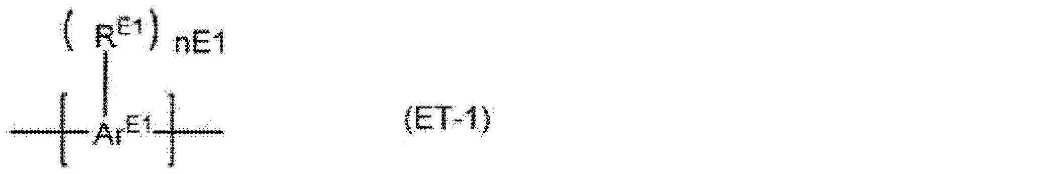
nE1は、1以上の整数を表す。
ArE1は、置換基を有していてもよい芳香族炭化水素基又は置換基を有していてもよい複素環基を表す。
RE1は、置換基を有していてもよいヘテロ原子を含む1価の基を表す。RE1が複数存在する場合、それらは同一でも異なっていてもよい。]

ArH1及びArH2は、それぞれ独立に、置換基を有していてもよい1価の芳香族炭化水素基又は置換基を有していてもよい1価の複素環基を表し、
LH1は、置換基を有していてもよい2価の芳香族炭化水素基又は置換基を有していてもよい2価の複素環基を表し、
LH2は、式:-N(-LH21-RH21)-
(式中、LH21は、単結合、置換基を有していてもよいアリーレン基又は置換基を有していてもよい2価の複素環基を表す。RH21は、水素原子、置換基を有していてもよいアルキル基、置換基を有していてもよいシクロアルキル基、置換基を有していてもよいアリール基又は置換基を有していてもよい1価の複素環基を表す。)
で表される基を表す。
LH1が複数存在する場合、それらは同一でも異なっていてもよい。LH2が複数存在する場合、それらは同一でも異なっていてもよい。
nH1、nH2及びnH3は、それぞれ独立に、0以上10以下の整数を表す。]
本明細書で共通して用いられる用語は、特記しない限り、以下の意味である。
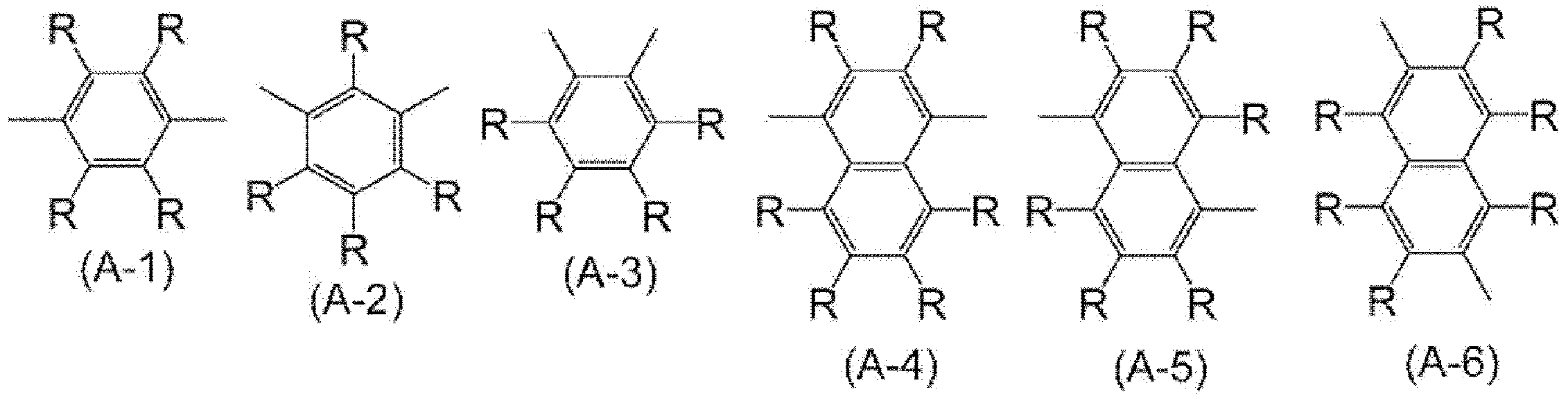


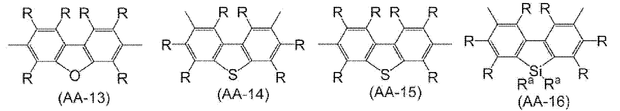


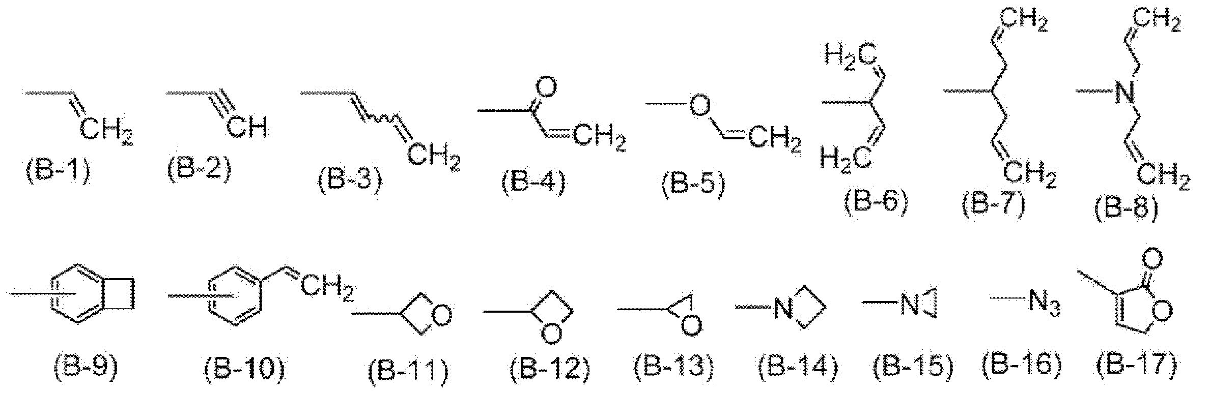
本実施形態に係る発光素子は、陽極、発光層、電子輸送層及び陰極を有する。本実施形態に係る発光素子において、電子輸送層は、粒子と非粒子性の電子輸送性材料とを含む。
本実施形態において、発光素子の光取り出し効率の観点から、電子輸送層に含まれる粒子の波長550nmの光の屈折率は、非粒子性の電子輸送性材料の波長550nmの光の屈折率よりも0.15以上小さく、0.18以上小さいことが好ましく、0.20以上小さいことがより好ましい。
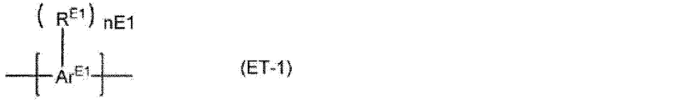
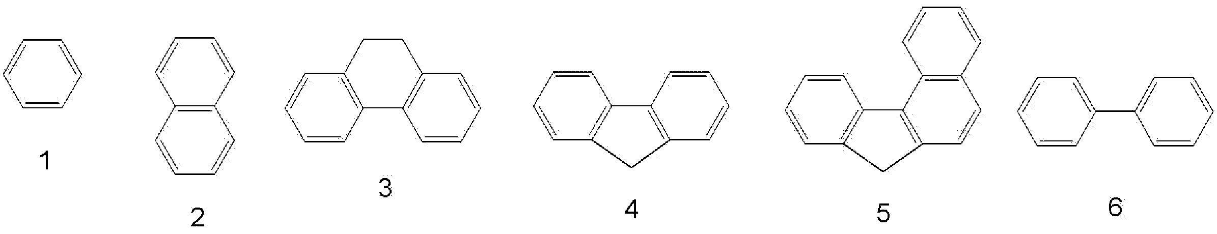


-C(=O)-(R’-C(=O))q-R’’ (IV)
-C(=S)-(R’-C(=S))q-R’’ (V)
-N{(R’)qR’’}2 (VI)
-C(=O)O-(R’-C(=O)O)q-R’’ (VII)
-C(=O)-O-(R’O)q-R’’ (VIII)
-NHC(=O)-(R’NHC(=O))q-R’’ (IX)
[式中、
R’は置換基を有していてもよいヒドロカルビレン基を表す。
R’’は水素原子、置換基を有していてもよいヒドロカルビル基、カルボキシル基、スルホ基、水酸基、メルカプト基、アミノ基、-NRc 2で表される基、シアノ基又は-C(=O)NRc 2で表される基を表す。
R’’’は置換基を有していてもよい3価の炭化水素基を表す。
mは1以上の整数を表す。
qは0以上の整数を表す。
Rcは置換基を有していてもよい炭素原子数1~30のアルキル基又は置換基を有していてもよい炭素原子数6~50のアリール基を表す。
R’、R’’及びR’’’の各々が複数個存在する場合、同一でも異なっていてもよい。]


M+が複数存在する場合、それらは同一でも異なっていてもよい。]

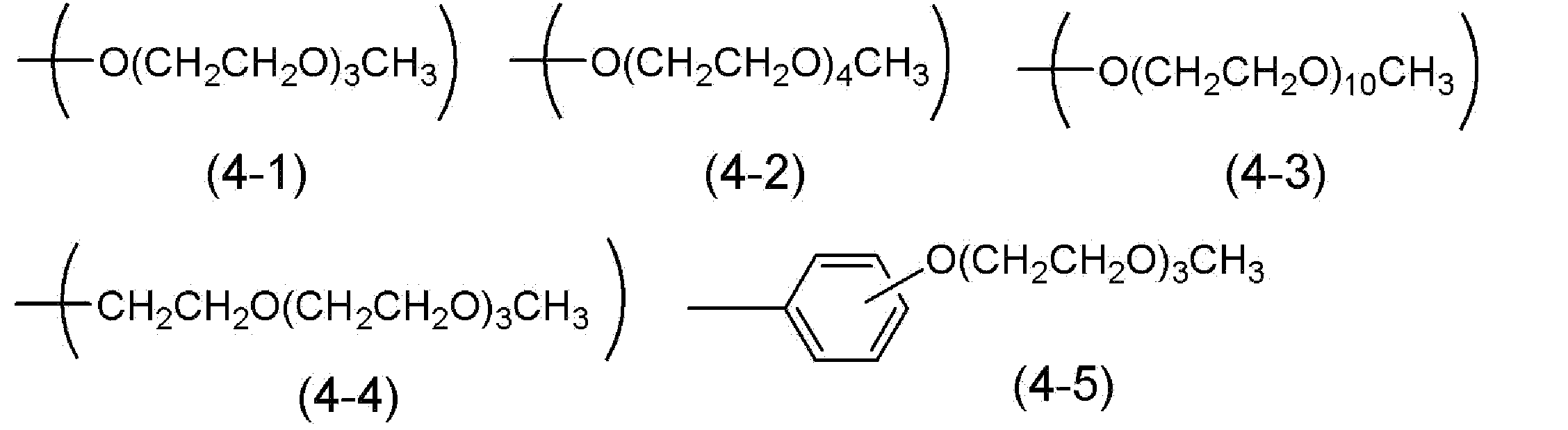
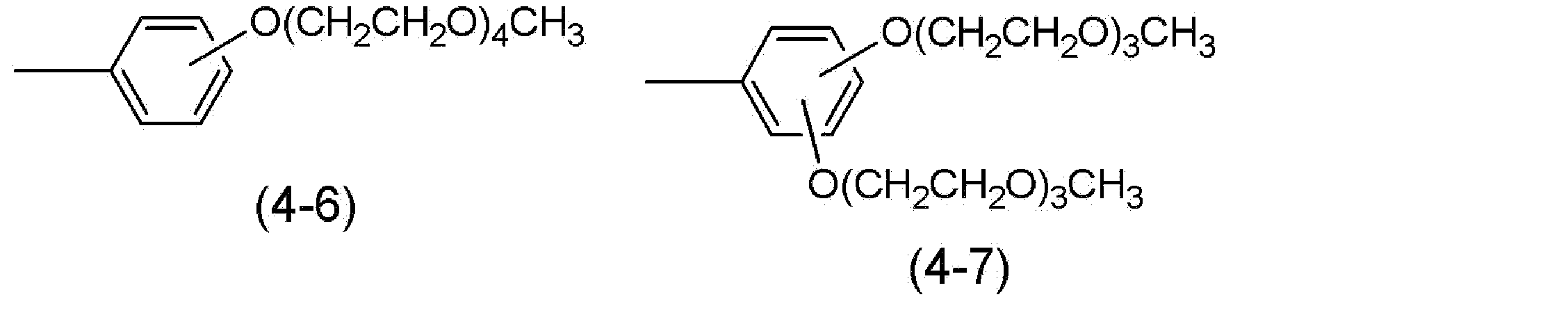
式(ET-1)で表される構成単位としては、例えば、下記式で表される構成単位が挙げられる。

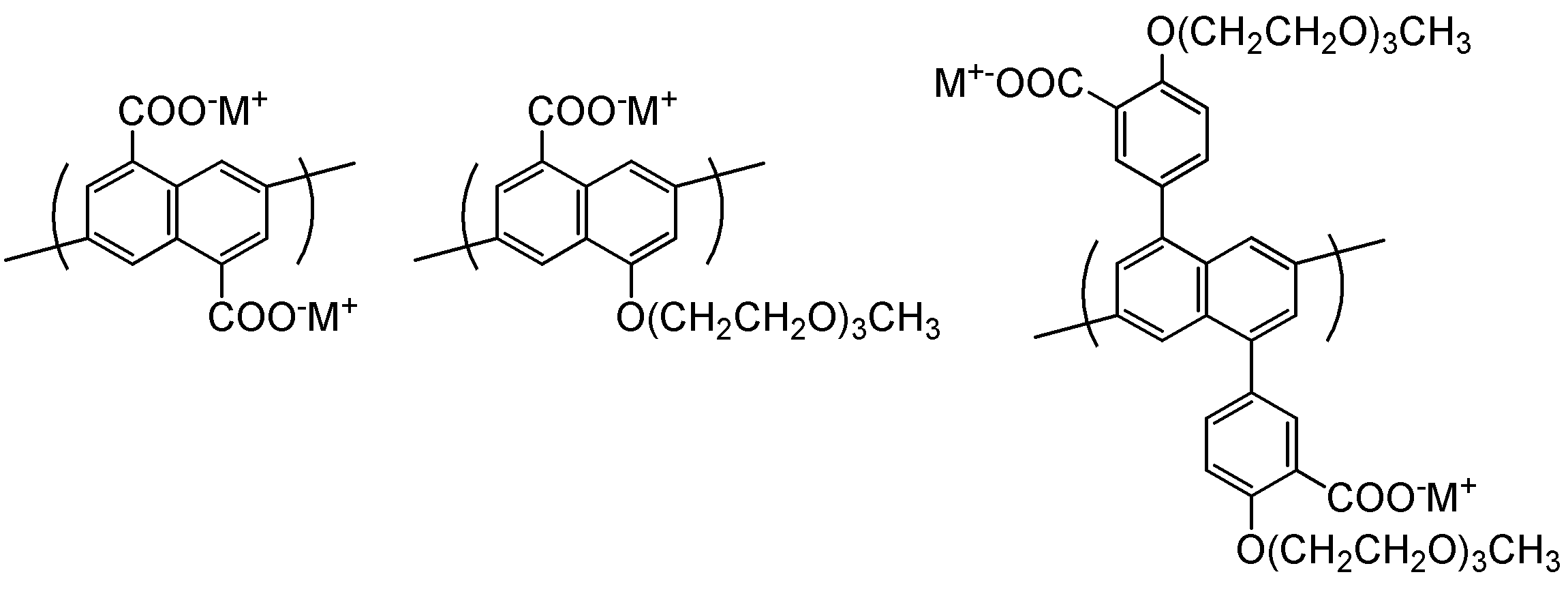
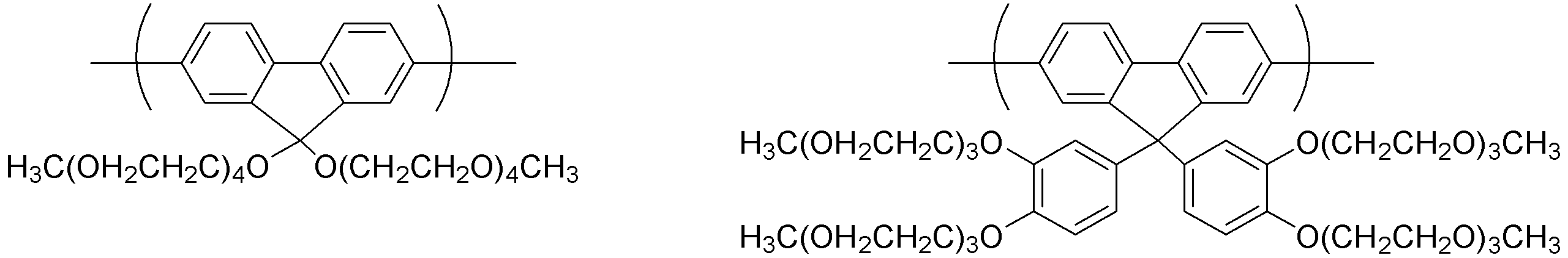
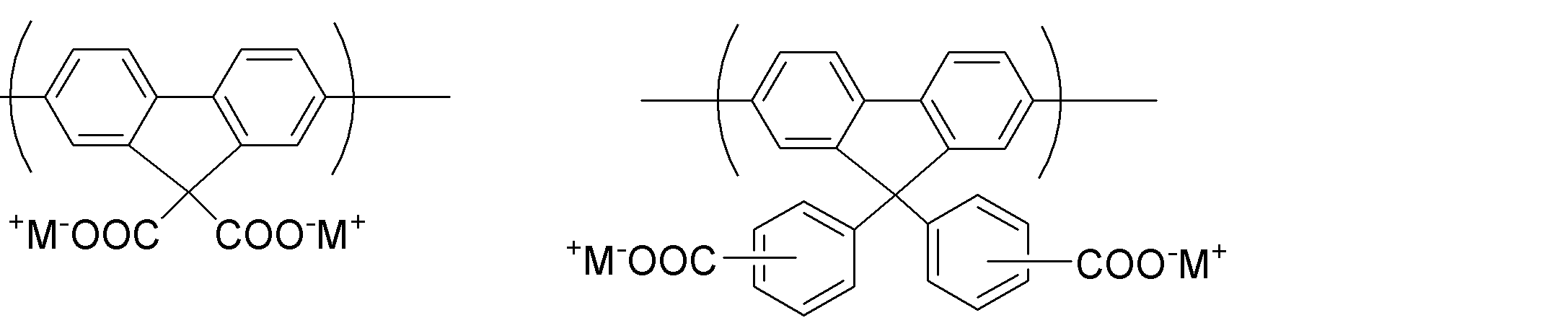


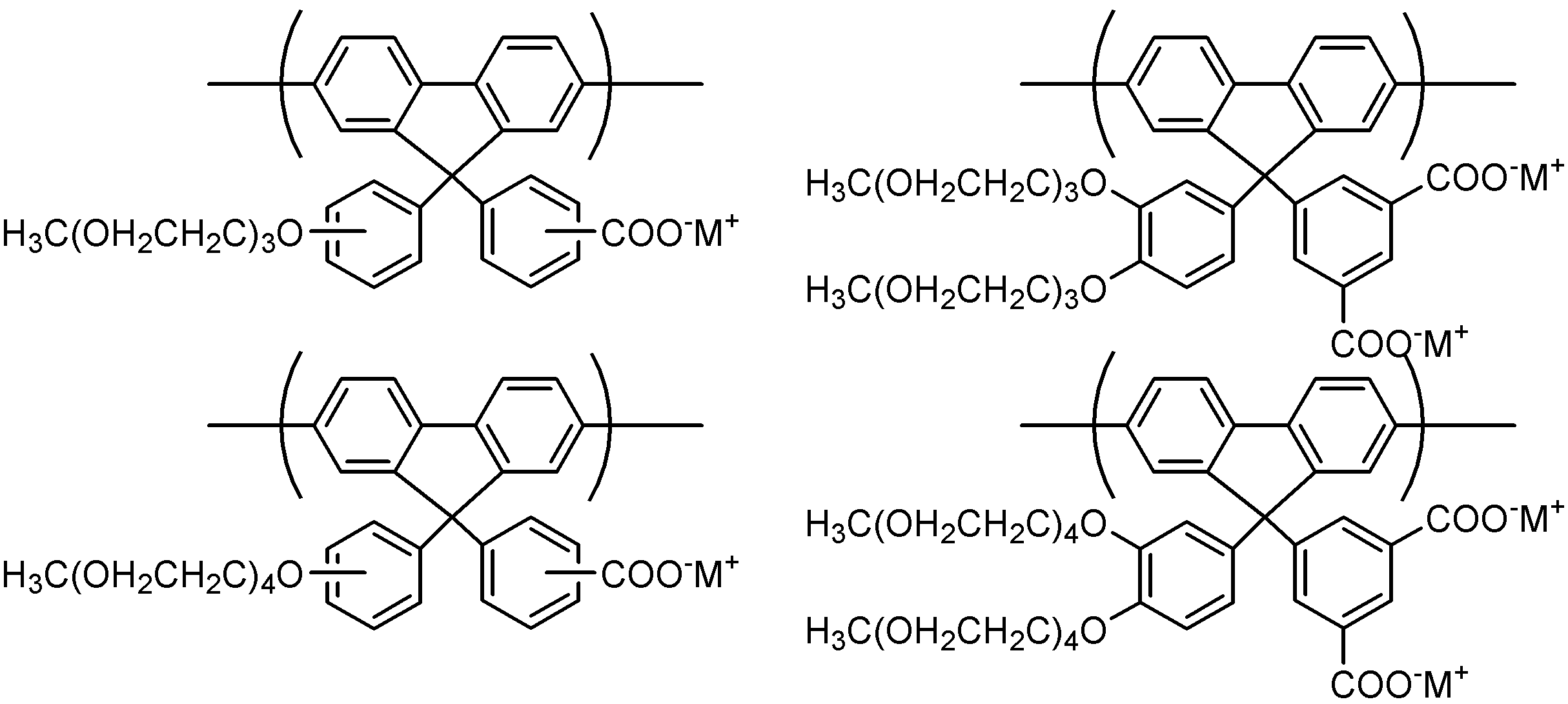

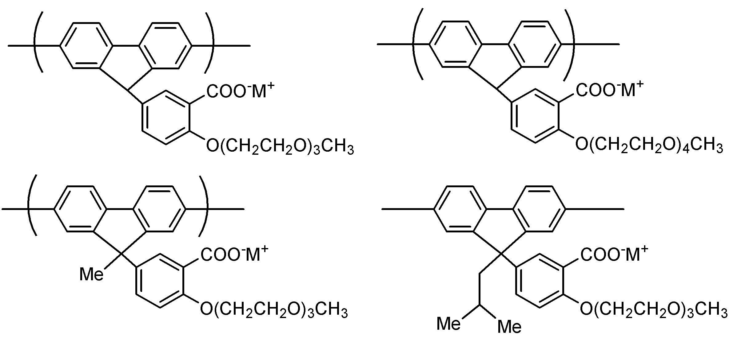
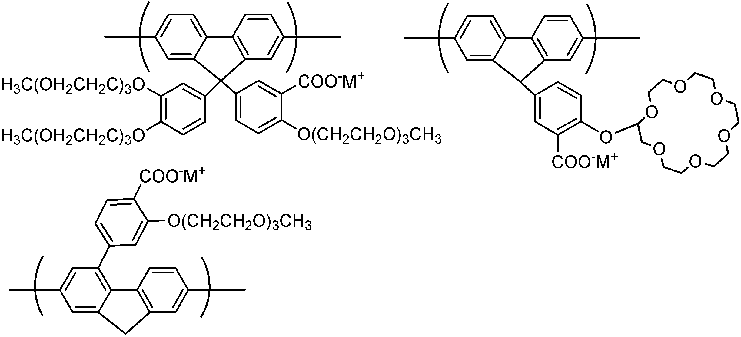
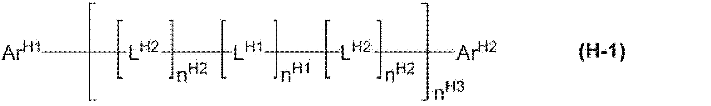


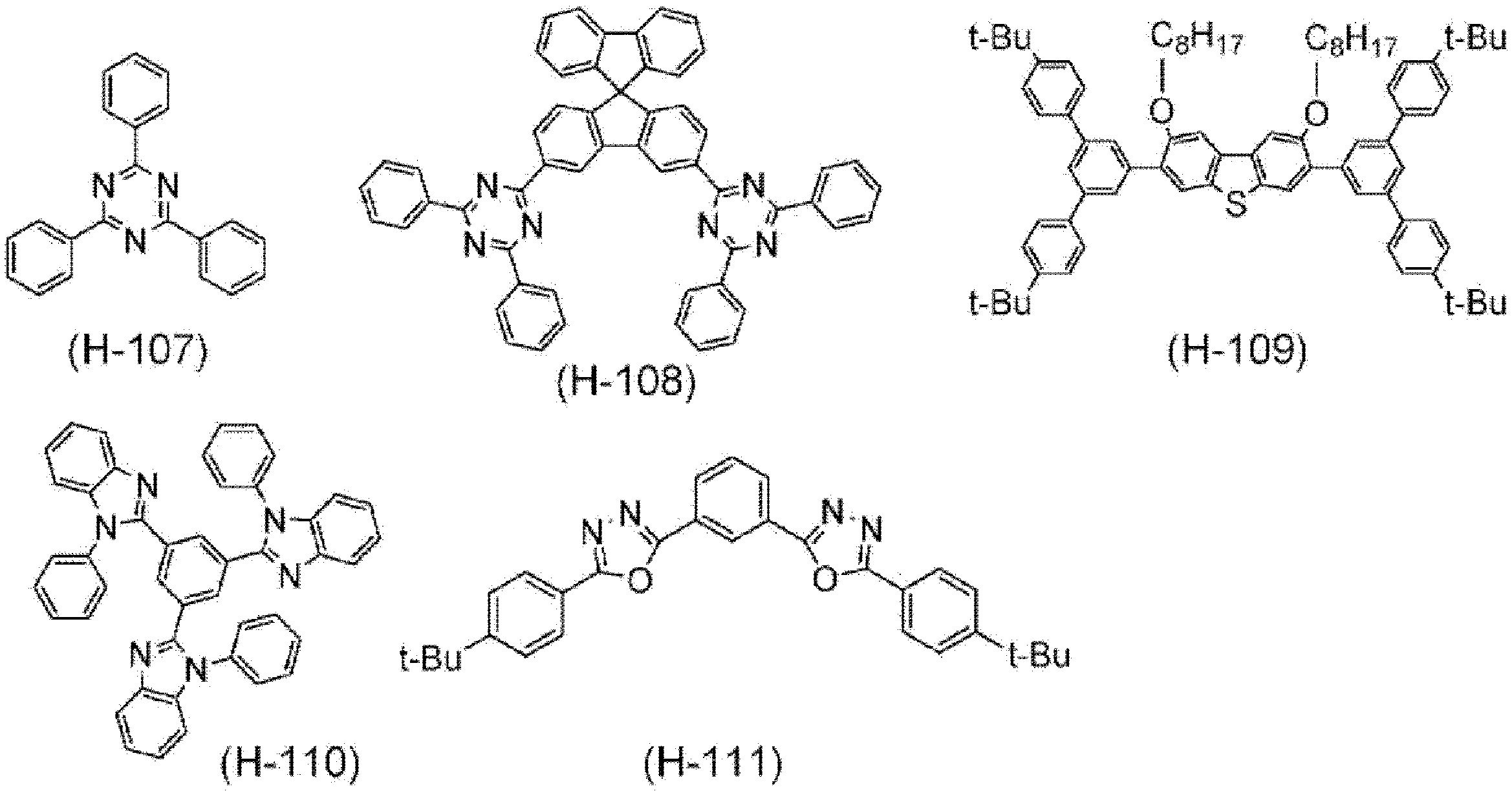
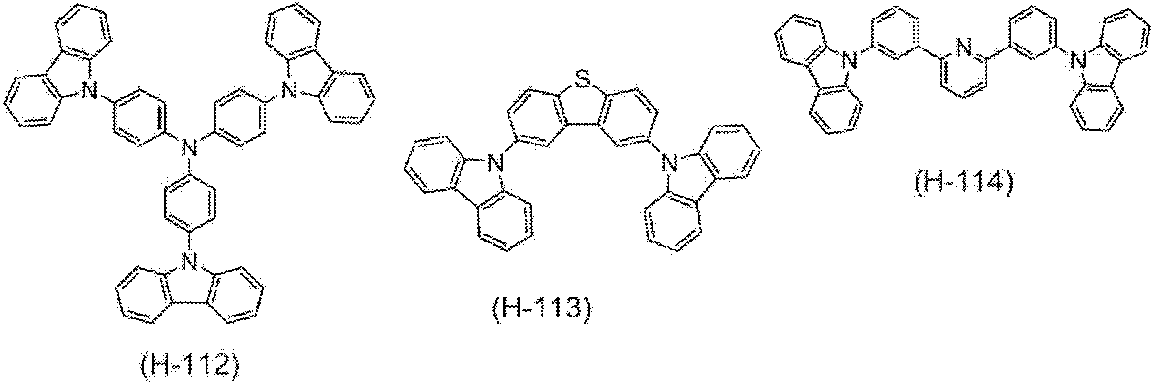

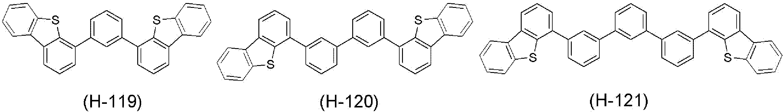

本実施形態において、発光層は、発光材料を含む層であってよい。発光材料は、低分子化合物と高分子化合物とに分類される。発光材料は、高分子化合物であっても低分子化合物であってもよい。また、発光材料は、架橋性基を有していてよく、架橋性基により架橋されていてもよい。


RD1~RD8、RD11~RD20、RD21~RD26及びRD31~RD37は、それぞれ独立に、水素原子、アルキル基、シクロアルキル基、アルコキシ基、シクロアルコキシ基、アリール基、アリールオキシ基、1価の複素環基又はハロゲン原子を表し、これらの基における水素原子の一部又は全部(例えば、1個~置換され得る全ての水素原子)は置換基で置換されていてもよい。RD1~RD8、RD11~RD20、RD21~RD26及びRD31~RD37が複数存在する場合、それらはそれぞれ同一でも異なっていてもよい。
-AD1---AD2-は、アニオン性の2座配位子を表し、AD1及びAD2は、それぞれ独立に、イリジウム原子と結合する炭素原子、酸素原子又は窒素原子を表し、これらの原子は環を構成する原子であってもよい。-AD1---AD2-が複数存在する場合、それらは同一でも異なっていてもよい。
nD1は、1、2又は3を表し、nD2は、1又は2を表す。]


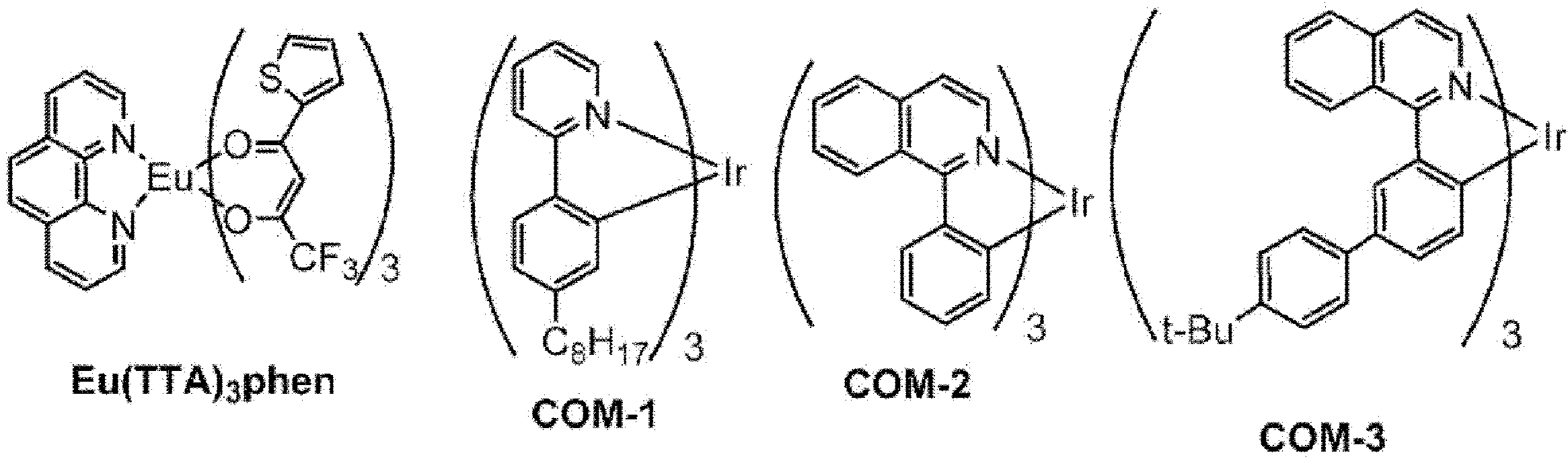

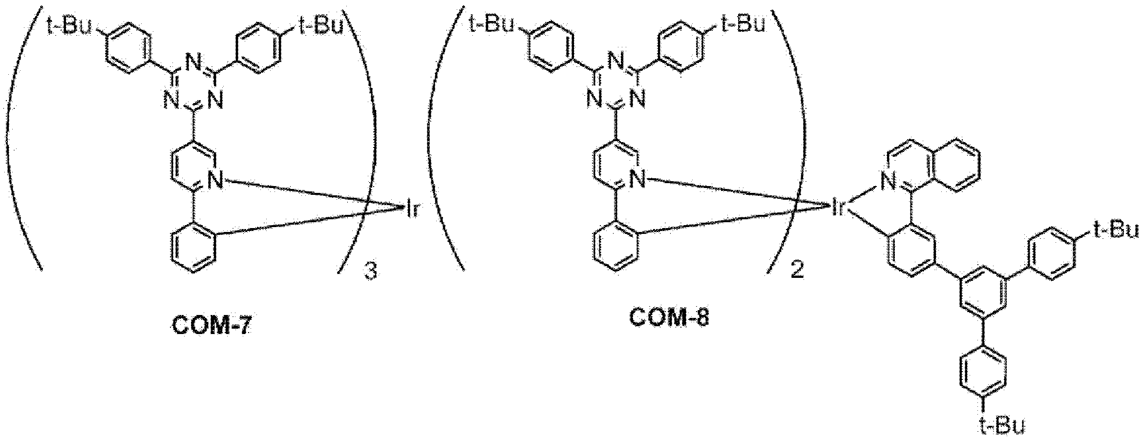


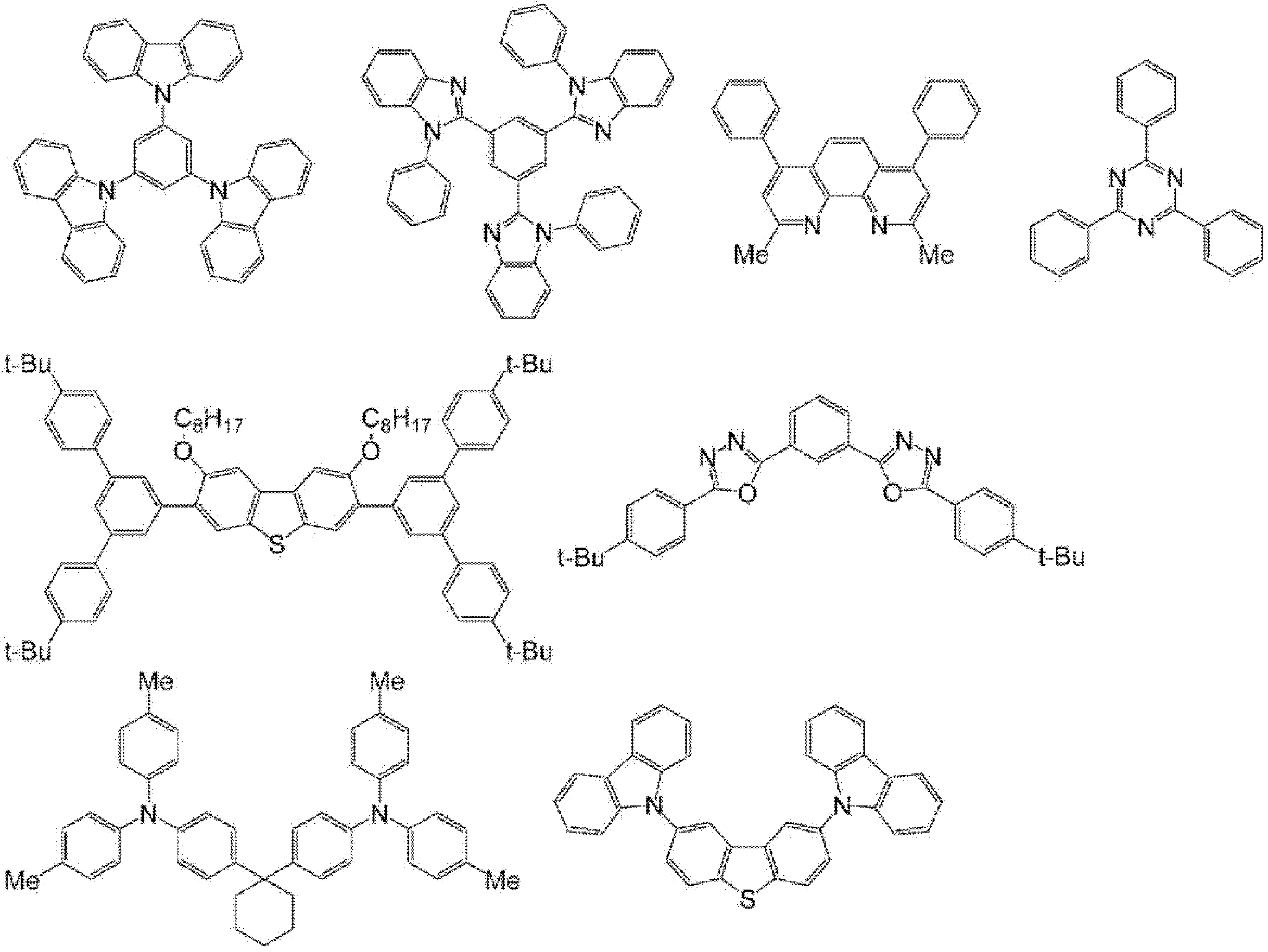
本実施形態に係る発光素子は、陽極及び陰極を有している。
正孔注入層とは、陽極に隣接する層であり、陽極から正孔を受け取る機能を有する層であり、さらに必要に応じて正孔を輸送する機能、発光層へ正孔を供給する機能、陰極から注入された電子を障壁する機能のいずれかを有する層をいう。正孔輸送層とは、主に正孔を輸送する機能を有する層であり、さらに必要に応じて、陽極から正孔を受け取る機能、発光層へ正孔を供給する機能、陰極から注入された電子を障壁する機能のいずれかを有する層をいう。
本実施形態に係る発光素子において、正孔輸送層を構成する材料としては、例えば、カルバゾール及びその誘導体、トリアゾール及びその誘導体、オキサゾール及びその誘導体、オキサジアゾール及びその誘導体、イミダゾール及びその誘導体、フルオレン及びその誘導体、ポリアリールアルカン及びその誘導体、ピラゾリン及びその誘導体、ピラゾロン及びその誘導体、フェニレンジアミン及びその誘導体、アリールアミン及びその誘導体、アミノ置換カルコン及びその誘導体、スチリルアントラセン及びその誘導体、フルオレノン及びその誘導体、ヒドラゾン及びその誘導体、スチルベン及びその誘導体、シラザン及びその誘導体、芳香族第三級アミン化合物、スチリルアミン化合物、芳香族ジメチリディン系化合物、ポルフィリン系化合物、ポリシラン系化合物、ポリ(N-ビニルカルバゾール)及びその誘導体、有機シラン及びその誘導体、及びこれらの構造を含む重合体;アニリン系共重合体、チオフェンオリゴマー、ポリチオフェン等の導電性高分子及びオリゴマー;ポリピロール等の有機導電性材料が挙げられる。これらの材料は単成分であっても或いは複数の成分からなる高分子化合物であってもよい。また、正孔輸送層は、これらの材料のみからなる単層構造であってもよいし、同一組成又は異種組成の複数層からなる多層構造であってもよい。また、正孔注入層で用いることができる材料として例示する材料も正孔輸送層で用いることができる。
(a)陽極-発光層-電子輸送層-陰極
(b)陽極-正孔注入層-発光層-電子輸送層-陰極
(c)陽極-正孔注入層-正孔輸送層-発光層-電子輸送層-陰極
(d)陽極-発光層-電子輸送層-電子注入層-陰極
(e)陽極-正孔注入層-発光層-電子輸送層-電子注入層-陰極
(f)陽極-正孔注入層-正孔輸送層-発光層-電子輸送層-電子注入層-陰極
NMRの測定は、約10mgの測定試料を約0.7mLの重溶媒に溶解させ、NMR装置(Agilent製、商品名:INOVA300又はMERCURY 400VX)を用いて行った。
TLC-MSの測定は、測定試料をトルエン、テトラヒドロフラン又はクロロホルムに任意の濃度で溶解させ、DART用TLCプレート(テクノアプリケーションズ社製、商品名:YSK5-100)上に塗布し、TLC-MS(日本電子社製、商品名:JMS-T100TD(The AccuTOF TLC))を用いて行った。測定時のヘリウムガス温度は、200~400℃の範囲で調節した。
化合物の純度の指標として、高速液体クロマトグラフィー(HPLC)面積百分率の値を用いた。この値は、特記しない限り、HPLC(島津製作所製、商品名:LC-20A)での254nmにおける値とする。この際、測定する化合物は、0.01~0.2質量%の濃度になるようにテトラヒドロフラン又はクロロホルムに溶解させ、HPLCに、濃度に応じて1~10μL注入した。HPLCの移動相には、アセトニトリル及びテトラヒドロフランを用い、1mL/分の流速で、アセトニトリル/テトラヒドロフラン=100/0~0/100(容積比)のグラジエント分析で流した。カラムは、SUMIPAX ODS Z-CLUE(住化分析センター製)又は同等の性能を有するODSカラムを用いた。検出器には、フォトダイオードアレイ検出器(島津製作所製、商品名:SPD-M20A)を用いた。
液体クロマトグラフ質量分析(LC-MS)は、測定試料を約2mg/mLの濃度になるようにクロロホルム又はTHFに溶解させ、LC-MS(アジレントテクノロジー製、商品名:1100LCMSD)に約1μL注入し、LC-MSの移動相には、アセトニトリル及びTHFの比率を変化させながら用い、0.2mL/分の流量で流すことにより行った。カラムは、SUMIPAX ODS Z-CLUE(φ4.6×250mm、3μm、住化分析センター製)を用いた。
Z平均粒子径の測定は、測定試料の粒子を約1質量%以下の濃度になるように分散可能な溶媒で分散させ、ゼータサイザー(マルバーン製、商品名:ゼータサイザーナノZS)を用いて行った。
自乗平均粗さ、最大高低差、電子輸送層における単位面積あたりの粒子の数(本明細書において、単位面積あたりの粒子の数を「粒子の密度」と言うこともある)の測定は、下記の方法で行った。
単量体CM1~CM6は、下記文献に記載された方法に従って合成し、それぞれ99.5%以上のHPLC面積百分率値を示したものを用いた。
単量体CM1は、特開2012-033845号公報記載の方法に従って合成した。
単量体CM2は、特開2010-189630号公報記載の方法に従って合成した。
単量体CM3~CM5は、国際公開第2013/146806号に記載の方法に従って合成した。
単量体CM6は、国際公開第2009/157424号に記載の方法に従って合成した。


反応容器内を不活性ガス雰囲気とした後、単量体CM1(9.23g)、単量体CM2(4.58g)、ジクロロビス(トリス-o-メトキシフェニルホスフィン)パラジウム(8.6mg)及びトルエン(175mL)を加え、105℃に加熱した。その後、そこに、12質量%炭酸ナトリウム水溶液(40.3mL)を滴下し、29時間還流させた。その後、そこに、フェニルボロン酸(0.47g)及びジクロロビス(トリス-o-メトキシフェニルホスフィン)パラジウム(8.7mg)を加え、14時間還流させた。

反応容器内を不活性ガス雰囲気とした後、単量体CM3(2.52g)、単量体CM4(0.47g)、単量体CM5(4.90g)、単量体CM6(0.53g)、及びトルエン(158mL)を加え、95℃に加熱した。反応液に、20質量%水酸化テトラエチルアンモニウム水溶液(16mL)、ジクロロビス(トリス-o-メトキシフェニルホスフィン)パラジウム(4.2mg)を加え、8時間還流させた。反応後、そこに、フェニルボロン酸(0.12g)、20質量%水酸化テトラエチルアンモニウム水溶液(16mL)、及びジクロロビス(トリス-o-メトキシフェニルホスフィン)パラジウム(4.2mg)を加え、15時間還流させた。その後、そこに、ジエチルジチアカルバミン酸ナトリウム水溶液を加え、85℃で2時間撹拌した。冷却後、反応液を、3.6質量%塩酸水溶液で2回、2.5質量%アンモニア水溶液で2回、水で4回洗浄し、得られた溶液をメタノールに滴下したところ、沈澱が生じた。沈殿物をトルエンに溶解させ、アルミナカラム、シリカゲルカラムの順番で通すことにより精製した。得られた溶液をメタノールに滴下し、撹拌した後、得られた沈殿物をろ取し、乾燥させることにより、高分子化合物H1(6.02g)を得た。測定条件1により測定した高分子化合物H1のMnは3.8×104であり、Mwは4.5×105であった。
燐光発光性化合物1及び2は、下記文献に記載された方法に従って合成し、それぞれ99.5%以上のHPLC面積百分率値を示したものを用いた。

フラスコを不活性雰囲気下にした後、2,8-ジブロモ-4-ブチルジベンゾチオフェン 8.7g(0.022mol)と、4-アザ-1H-カルバゾール 8.1g(0.048mol)を218mLのジメチルスルホキシドに溶解させた。Cu2O 1.3g(0.009mol)とリン酸三カリウム 16.7g(0.079mol)を加えた後、ジピバロイルメタン 3.2g(0.018mol)を加え、150℃のオイルバスにつけ加熱した。
(i)陽極及び正孔注入層の形成
ガラス基板にスパッタ法により45nmの厚みでITO膜を付けることにより陽極を形成した。陽極上に、日産化学工業株式会社製の正孔注入材料(ND-3202)を、スピンコート法にて膜厚35nmに成膜した。正孔注入材料が成膜された基板をホットプレート上で50℃で3分間加熱して溶媒を揮発させ、続けてホットプレートにて240℃で15分間加熱することにより正孔注入層を形成した。
キシレンに、高分子化合物H1を0.65質量%の濃度で溶解させた。得られたキシレン溶液を用いて、正孔注入層の上に、スピンコート法により20nmの厚さで成膜し、窒素ガス雰囲気下、ホットプレート上で180℃、60分間加熱させることにより正孔輸送層を形成した。
トルエンに、下記式:

2,2,3,3,4,4,5,5-オクタフルオロ-1-ペンタノール100質量部に高分子化合物E1(屈折率1.71)を0.5質量部溶解させ、加えて0.5質量部のシリカ粒子(信越化学工業株式会社製のQSG-170 屈折率1.46、Z平均粒子径199nm)を分散させて得られた分散液を用いて、発光層の上に、スピンコート法で高分子化合物E1が20nmの厚さとなるように成膜し、窒素ガス雰囲気下、130℃、10分間加熱することにより電子輸送層を形成した。本電子輸送層中の、電子輸送性材料である高分子化合物E1の100質量部に対する、粒子の質量は100質量部である。
電子輸送層が形成された基板を蒸着機内に置いて、1.0×10⁻⁴Pa以下に減圧した後、陰極として、電子輸送層の上にフッ化ナトリウムを約4nm、次いで、その上にアルミニウムを約100nm蒸着した。その後、ガラス基板を用いて封止することにより、発光素子D1を作製した。得られた発光素子D1において、単位面積当たりのシリカ粒子の数は、2.3個/μm2であった。また、前記陰極又は電子注入層と前記電子輸送層との界面の自乗平均粗さは、38.3nmであった。
電子輸送層にシリカ粒子を配合しなかったこと以外は、実施例1と同様にして、発光素子CD1を作製した。得られた発光素子CD1において、単位面積当たりの粒子の数は、0個/μm2であった。また、前記陰極又は電子注入層と前記電子輸送層との界面の自乗平均粗さは、1nm以下であった。
陰極として、電子輸送層の上にフッ化ナトリウムを約4nm、次いで、その上にアルミニウムを約100nm蒸着する代わりに、電子輸送層の上にフッ化ナトリウム4nm、次いで、その上にマグネシウム約1nm、その上にアルミニウムを約100nm蒸着した以外は、実施例1と同様にして、発光素子D2を作製した。発光素子D2において、単位面積当たりのシリカ粒子の数、前記陰極又は電子注入層と前記電子輸送層との界面の自乗平均粗さは、実施例1と同様であった。
電子輸送層にシリカ粒子を配合しなかったこと以外は、実施例2と同様にして、発光素子CD2を作製した。
電子輸送層に用いる高分子化合物E1の代わりに、低分子化合物E2(屈折率約1.70)を同質量部用いた以外は、実施例1と同様にして、発光素子D3を作製した。発光素子D3において、単位面積当たりのシリカ粒子の数は、1.8個/μm2であった。また、前記陰極又は電子注入層と前記電子輸送層との界面の自乗平均粗さは、35.8nmであった。
電子輸送層にシリカ粒子を配合しなかったこと以外は、実施例3と同様にして、発光素子CD3を作製した。
電子輸送層に用いる低分子化合物E2の100質量部に対するシリカ粒子の質量部を、表4に記載の通り変更した以外は、実施例3と同様にして、発光素子D4~D11を作製した。
電子輸送層に用いる低分子化合物E2の100質量部に対するシリカ粒子の質量部を250質量部に変更した以外は、実施例3と同様にして、発光素子CD4を作製した。
電子輸送層に用いるシリカ粒子(信越化学工業株式会社製のQSG-170 屈折率1.46、Z平均粒子径199nm)の代わりに、シリカ粒子(コアフロント社製のSicastar 屈折率1.46、動的光散乱法による平均粒子径300nm(カタログ値))を用いた以外は、実施例3と同様にして、発光素子D12を作製した。
発光素子D1~D3、CD1~CD3に電圧を印加することにより、EL発光が観測された。発光素子の1000cd/m2における発光効率(cd/A)と、電子輸送層に用いた電子輸送性材料と粒子、電子注入層を含めた陰極の構造、粒子の屈折率と電子輸送層の屈折率の屈折率差(n1-n2)を表1から表3に示す。


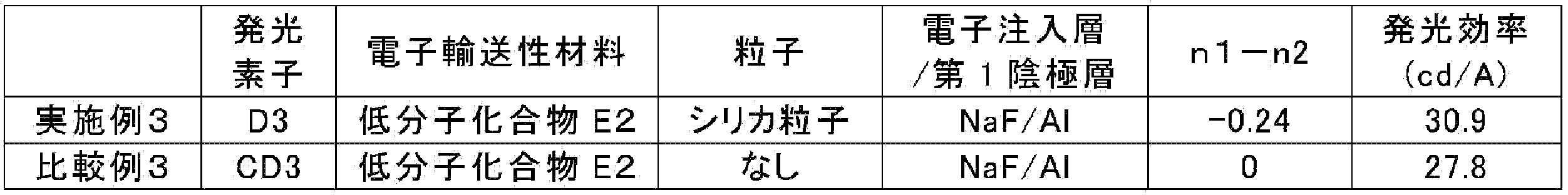
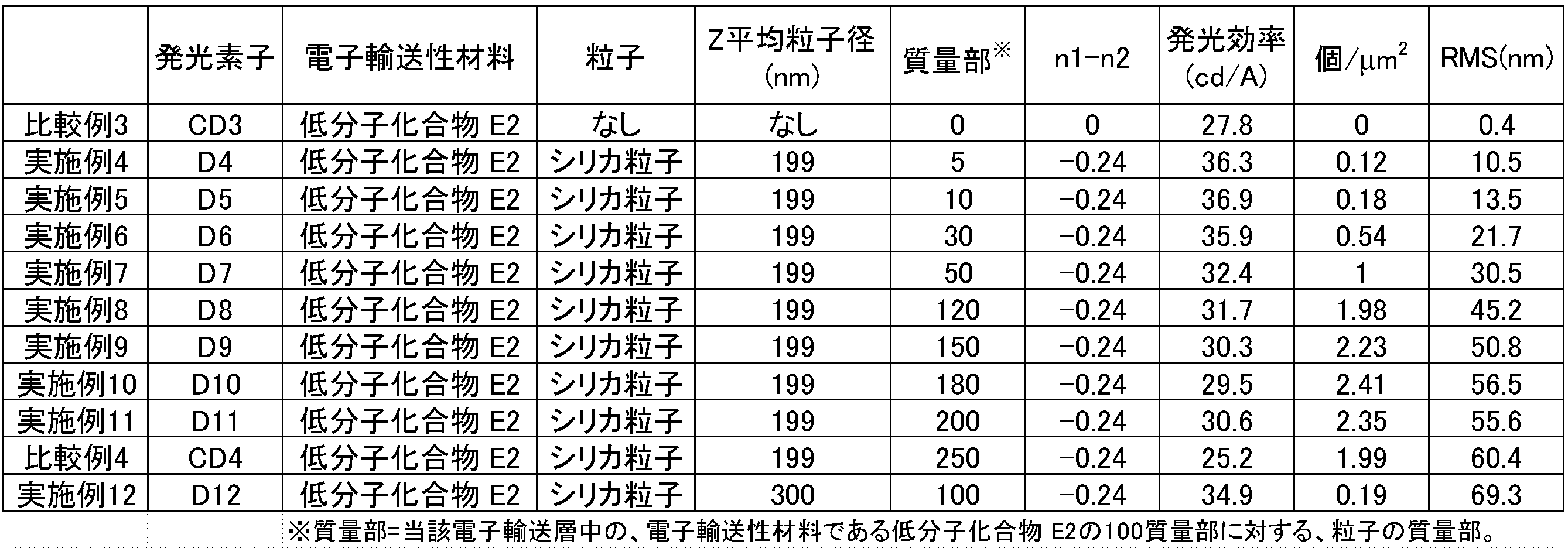
Claims (8)
- 陰極、電子輸送層、発光層及び陽極がこの順番に配置されている発光素子であって、
前記発光素子は、前記陰極と前記電子輸送層との間にさらに電子注入層を有していてもよく、
前記電子輸送層が、粒子と非粒子性の電子輸送性材料とを含み、
前記粒子を構成する材料の波長550nmの光の屈折率n1及び前記非粒子性の電子輸送性材料の波長550nmの光の屈折率n2が、
n1-n2≦-0.15
の関係を満たし、
前記粒子の動的光散乱法により求めたZ平均粒子径が110~300nmである、
前記発光素子。 - 前記粒子を構成する材料の波長550nmの光の屈折率n1が1.5以下である、請求項1に記載の発光素子。
- 前記粒子が、シリカ粒子である請求項1又は2に記載の発光素子。
- 前記電子輸送性材料が、式(ET-1)で表される構成単位を有する高分子化合物を含む、請求項1~3のいずれか一項に記載の発光素子。
[式中、 nE1は、1以上の整数を表す。
ArE1は、置換基を有していてもよい芳香族炭化水素基又は置換基を有していてもよい複素環基を表す。
RE1は、置換基を有していてもよいヘテロ原子を含む1価の基を表す。RE1が複数存在する場合、それらは同一でも異なっていてもよい。] - 前記電子輸送性材料が式(H-1)で表される化合物を含む、請求項1~4のいずれか一項に記載の発光素子。
[式中、 ArH1及びArH2は、それぞれ独立に、置換基を有していてもよい1価の芳香族炭化水素基又は置換基を有していてもよい1価の複素環基を表し、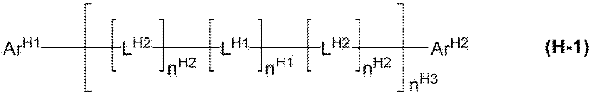
LH1は、置換基を有していてもよい2価の芳香族炭化水素基又は置換基を有していてもよい2価の複素環基を表し、
LH2は、式:-N(-LH21-RH21)-
(式中、LH21は、単結合、置換基を有していてもよいアリーレン基又は置換基を有していてもよい2価の複素環基を表す。RH21は、水素原子、置換基を有していてもよいアルキル基、置換基を有していてもよいシクロアルキル基、置換基を有していてもよいアリール基又は置換基を有していてもよい1価の複素環基を表す。)
で表される基を表す。
LH1が複数存在する場合、それらは同一でも異なっていてもよい。LH2が複数存在する場合、それらは同一でも異なっていてもよい。
nH1、nH2及びnH3は、それぞれ独立に、0以上10以下の整数を表す。] - 前記電子輸送性材料100質量部に対して、前記粒子の割合が1~200質量部である、請求項1~5のいずれか一項に記載の発光素子。
- 前記電子輸送層における単位面積あたりの前記粒子の数が1個/μm2以上である、請求項1~6のいずれか一項に記載の発光素子。
- 前記陰極又は前記電子注入層と前記電子輸送層とが隣接し、かつ、前記陰極又は前記電子注入層と前記電子輸送層との界面の自乗平均粗さが5nm以上である、請求項1~7のいずれか一項に記載の発光素子。
Priority Applications (5)
| Application Number | Priority Date | Filing Date | Title |
|---|---|---|---|
| EP18871468.7A EP3703146A4 (en) | 2017-10-27 | 2018-10-17 | LUMINESCENT ELEMENT |
| CN201880069240.3A CN111279506A (zh) | 2017-10-27 | 2018-10-17 | 发光元件 |
| KR1020207014660A KR20200074192A (ko) | 2017-10-27 | 2018-10-17 | 발광 소자 |
| JP2019551057A JPWO2019082769A1 (ja) | 2017-10-27 | 2018-10-17 | 発光素子 |
| US16/758,846 US20200266378A1 (en) | 2017-10-27 | 2018-10-17 | Light-emitting element |
Applications Claiming Priority (2)
| Application Number | Priority Date | Filing Date | Title |
|---|---|---|---|
| JP2017-208611 | 2017-10-27 | ||
| JP2017208611 | 2017-10-27 |
Publications (1)
| Publication Number | Publication Date |
|---|---|
| WO2019082769A1 true WO2019082769A1 (ja) | 2019-05-02 |
Family
ID=66246481
Family Applications (1)
| Application Number | Title | Priority Date | Filing Date |
|---|---|---|---|
| PCT/JP2018/038710 WO2019082769A1 (ja) | 2017-10-27 | 2018-10-17 | 発光素子 |
Country Status (6)
| Country | Link |
|---|---|
| US (1) | US20200266378A1 (ja) |
| EP (1) | EP3703146A4 (ja) |
| JP (1) | JPWO2019082769A1 (ja) |
| KR (1) | KR20200074192A (ja) |
| CN (1) | CN111279506A (ja) |
| WO (1) | WO2019082769A1 (ja) |
Citations (16)
| Publication number | Priority date | Publication date | Assignee | Title |
|---|---|---|---|---|
| WO2006121811A1 (en) | 2005-05-06 | 2006-11-16 | Universal Display Corporation | Stability oled materials and devices with improved stability |
| JP2007242927A (ja) * | 2006-03-09 | 2007-09-20 | Seiko Epson Corp | 発光装置及び発光装置の製造方法 |
| JP2009239279A (ja) | 2008-03-07 | 2009-10-15 | Sumitomo Chemical Co Ltd | 積層構造体 |
| WO2009131255A1 (ja) | 2008-04-25 | 2009-10-29 | 住友化学株式会社 | 含窒素複素環式化合物の残基を有する高分子化合物 |
| WO2009157424A1 (ja) | 2008-06-23 | 2009-12-30 | 住友化学株式会社 | 金属錯体の残基を含む高分子化合物及びそれを用いた素子 |
| JP2010189630A (ja) | 2009-01-20 | 2010-09-02 | Sumitomo Chemical Co Ltd | メタフェニレン系高分子化合物及びそれを用いた発光素子 |
| JP2012033845A (ja) | 2009-09-30 | 2012-02-16 | Sumitomo Chemical Co Ltd | 積層構造体、重合体、電界発光素子及び光電変換素子 |
| JP2012216815A (ja) | 2011-03-28 | 2012-11-08 | Sumitomo Chemical Co Ltd | 電子デバイス、高分子化合物 |
| JP2012216821A (ja) | 2011-03-28 | 2012-11-08 | Sumitomo Chemical Co Ltd | 電子デバイス、高分子化合物 |
| JP2012216822A (ja) | 2011-03-28 | 2012-11-08 | Sumitomo Chemical Co Ltd | 電子デバイス、高分子化合物 |
| WO2013108618A1 (ja) * | 2012-01-19 | 2013-07-25 | パナソニック株式会社 | 有機el素子及びその製造方法 |
| WO2013146806A1 (ja) | 2012-03-27 | 2013-10-03 | 住友化学株式会社 | 高分子化合物およびそれを用いた発光素子 |
| US20140061592A1 (en) | 2012-08-29 | 2014-03-06 | General Electric Company | Oled devices with internal outcoupling |
| JP2014528633A (ja) * | 2011-09-30 | 2014-10-27 | ゼネラル・エレクトリック・カンパニイ | 中空体を含むoledデバイス |
| JP2015514293A (ja) * | 2012-03-23 | 2015-05-18 | エルジー・ケム・リミテッド | 有機発光素子 |
| WO2018135580A1 (ja) * | 2017-01-18 | 2018-07-26 | 日産化学工業株式会社 | 電荷輸送性ワニス及びそれを用いる電荷輸送性薄膜 |
Family Cites Families (2)
| Publication number | Priority date | Publication date | Assignee | Title |
|---|---|---|---|---|
| EP2287939A4 (en) * | 2008-05-21 | 2011-08-10 | Pioneer Corp | ORGANIC ELECTROLUMINESCENT ELEMENT |
| JPWO2013042745A1 (ja) * | 2011-09-21 | 2015-03-26 | パナソニックIpマネジメント株式会社 | 有機エレクトロルミネッセンス素子 |
-
2018
- 2018-10-17 US US16/758,846 patent/US20200266378A1/en not_active Abandoned
- 2018-10-17 WO PCT/JP2018/038710 patent/WO2019082769A1/ja unknown
- 2018-10-17 CN CN201880069240.3A patent/CN111279506A/zh active Pending
- 2018-10-17 EP EP18871468.7A patent/EP3703146A4/en not_active Withdrawn
- 2018-10-17 JP JP2019551057A patent/JPWO2019082769A1/ja active Pending
- 2018-10-17 KR KR1020207014660A patent/KR20200074192A/ko not_active Application Discontinuation
Patent Citations (16)
| Publication number | Priority date | Publication date | Assignee | Title |
|---|---|---|---|---|
| WO2006121811A1 (en) | 2005-05-06 | 2006-11-16 | Universal Display Corporation | Stability oled materials and devices with improved stability |
| JP2007242927A (ja) * | 2006-03-09 | 2007-09-20 | Seiko Epson Corp | 発光装置及び発光装置の製造方法 |
| JP2009239279A (ja) | 2008-03-07 | 2009-10-15 | Sumitomo Chemical Co Ltd | 積層構造体 |
| WO2009131255A1 (ja) | 2008-04-25 | 2009-10-29 | 住友化学株式会社 | 含窒素複素環式化合物の残基を有する高分子化合物 |
| WO2009157424A1 (ja) | 2008-06-23 | 2009-12-30 | 住友化学株式会社 | 金属錯体の残基を含む高分子化合物及びそれを用いた素子 |
| JP2010189630A (ja) | 2009-01-20 | 2010-09-02 | Sumitomo Chemical Co Ltd | メタフェニレン系高分子化合物及びそれを用いた発光素子 |
| JP2012033845A (ja) | 2009-09-30 | 2012-02-16 | Sumitomo Chemical Co Ltd | 積層構造体、重合体、電界発光素子及び光電変換素子 |
| JP2012216821A (ja) | 2011-03-28 | 2012-11-08 | Sumitomo Chemical Co Ltd | 電子デバイス、高分子化合物 |
| JP2012216815A (ja) | 2011-03-28 | 2012-11-08 | Sumitomo Chemical Co Ltd | 電子デバイス、高分子化合物 |
| JP2012216822A (ja) | 2011-03-28 | 2012-11-08 | Sumitomo Chemical Co Ltd | 電子デバイス、高分子化合物 |
| JP2014528633A (ja) * | 2011-09-30 | 2014-10-27 | ゼネラル・エレクトリック・カンパニイ | 中空体を含むoledデバイス |
| WO2013108618A1 (ja) * | 2012-01-19 | 2013-07-25 | パナソニック株式会社 | 有機el素子及びその製造方法 |
| JP2015514293A (ja) * | 2012-03-23 | 2015-05-18 | エルジー・ケム・リミテッド | 有機発光素子 |
| WO2013146806A1 (ja) | 2012-03-27 | 2013-10-03 | 住友化学株式会社 | 高分子化合物およびそれを用いた発光素子 |
| US20140061592A1 (en) | 2012-08-29 | 2014-03-06 | General Electric Company | Oled devices with internal outcoupling |
| WO2018135580A1 (ja) * | 2017-01-18 | 2018-07-26 | 日産化学工業株式会社 | 電荷輸送性ワニス及びそれを用いる電荷輸送性薄膜 |
Non-Patent Citations (4)
| Title |
|---|
| "Denki Kagaku Binran", 2000, MARUZEN |
| "Thermodynamic Database MALT", 1992, KAGAKU GIJUTSU-SHA |
| CHEMICAL REVIEWS (CHEM. REV., vol. 109, 2009, pages 897 - 1091 |
| See also references of EP3703146A4 |
Also Published As
| Publication number | Publication date |
|---|---|
| KR20200074192A (ko) | 2020-06-24 |
| EP3703146A1 (en) | 2020-09-02 |
| CN111279506A (zh) | 2020-06-12 |
| JPWO2019082769A1 (ja) | 2020-11-19 |
| US20200266378A1 (en) | 2020-08-20 |
| EP3703146A4 (en) | 2021-08-18 |
Similar Documents
| Publication | Publication Date | Title |
|---|---|---|
| JP6427681B2 (ja) | 組成物、燐光発光性化合物及び発光素子 | |
| JP6224758B2 (ja) | 発光素子及びその製造方法 | |
| JP2019108350A (ja) | 金属錯体および有機発光素子 | |
| US10756269B2 (en) | Composition and light emitting device using the same | |
| JP6642571B2 (ja) | 発光素子及びその製造方法 | |
| US20200407386A1 (en) | Composition and light emitting device using the same | |
| KR20200041329A (ko) | 발광 소자용 막 및 그것을 사용한 발광 소자 | |
| TW201839093A (zh) | 聚合電荷轉移層及包括其之有機電子裝置 | |
| EP3121182B1 (en) | Metal complex and light-emitting element using same | |
| JP2017108134A (ja) | 発光素子 | |
| WO2019082769A1 (ja) | 発光素子 | |
| WO2019082771A1 (ja) | 発光素子 | |
| EP3799142A1 (en) | Organic light emitting diode | |
| JP2020178100A (ja) | 発光素子 | |
| WO2017170314A1 (ja) | 発光素子 | |
| US20230192737A1 (en) | Metal complex, composition and light emitting element | |
| WO2020174837A1 (ja) | 発光素子 | |
| TW202102646A (zh) | 發光元件及發光元件用組成物 | |
| TW202348781A (zh) | 組成物及使用該組成物之發光元件的製造方法 | |
| JP2020010027A (ja) | 有機el素子用組成物 |
Legal Events
| Date | Code | Title | Description |
|---|---|---|---|
| 121 | Ep: the epo has been informed by wipo that ep was designated in this application |
Ref document number: 18871468 Country of ref document: EP Kind code of ref document: A1 |
|
| ENP | Entry into the national phase |
Ref document number: 2019551057 Country of ref document: JP Kind code of ref document: A |
|
| NENP | Non-entry into the national phase |
Ref country code: DE |
|
| ENP | Entry into the national phase |
Ref document number: 20207014660 Country of ref document: KR Kind code of ref document: A |
|
| ENP | Entry into the national phase |
Ref document number: 2018871468 Country of ref document: EP Effective date: 20200527 |