WO2019065355A1 - 吸着ステージ - Google Patents
吸着ステージ Download PDFInfo
- Publication number
- WO2019065355A1 WO2019065355A1 PCT/JP2018/034388 JP2018034388W WO2019065355A1 WO 2019065355 A1 WO2019065355 A1 WO 2019065355A1 JP 2018034388 W JP2018034388 W JP 2018034388W WO 2019065355 A1 WO2019065355 A1 WO 2019065355A1
- Authority
- WO
- WIPO (PCT)
- Prior art keywords
- suction
- semiconductor die
- valve
- vacuum
- adsorption
- Prior art date
- Legal status (The legal status is an assumption and is not a legal conclusion. Google has not performed a legal analysis and makes no representation as to the accuracy of the status listed.)
- Ceased
Links
Images





Classifications
-
- H—ELECTRICITY
- H10—SEMICONDUCTOR DEVICES; ELECTRIC SOLID-STATE DEVICES NOT OTHERWISE PROVIDED FOR
- H10P—GENERIC PROCESSES OR APPARATUS FOR THE MANUFACTURE OR TREATMENT OF DEVICES COVERED BY CLASS H10
- H10P72/00—Handling or holding of wafers, substrates or devices during manufacture or treatment thereof
- H10P72/70—Handling or holding of wafers, substrates or devices during manufacture or treatment thereof for supporting or gripping
- H10P72/78—Handling or holding of wafers, substrates or devices during manufacture or treatment thereof for supporting or gripping using vacuum or suction, e.g. Bernoulli chucks
-
- H—ELECTRICITY
- H10—SEMICONDUCTOR DEVICES; ELECTRIC SOLID-STATE DEVICES NOT OTHERWISE PROVIDED FOR
- H10P—GENERIC PROCESSES OR APPARATUS FOR THE MANUFACTURE OR TREATMENT OF DEVICES COVERED BY CLASS H10
- H10P72/00—Handling or holding of wafers, substrates or devices during manufacture or treatment thereof
- H10P72/04—Apparatus for manufacture or treatment
- H10P72/0446—Apparatus for mounting on conductive members, e.g. leadframes or conductors on insulating substrates
-
- H—ELECTRICITY
- H10—SEMICONDUCTOR DEVICES; ELECTRIC SOLID-STATE DEVICES NOT OTHERWISE PROVIDED FOR
- H10P—GENERIC PROCESSES OR APPARATUS FOR THE MANUFACTURE OR TREATMENT OF DEVICES COVERED BY CLASS H10
- H10P72/00—Handling or holding of wafers, substrates or devices during manufacture or treatment thereof
- H10P72/70—Handling or holding of wafers, substrates or devices during manufacture or treatment thereof for supporting or gripping
-
- H—ELECTRICITY
- H10—SEMICONDUCTOR DEVICES; ELECTRIC SOLID-STATE DEVICES NOT OTHERWISE PROVIDED FOR
- H10P—GENERIC PROCESSES OR APPARATUS FOR THE MANUFACTURE OR TREATMENT OF DEVICES COVERED BY CLASS H10
- H10P72/00—Handling or holding of wafers, substrates or devices during manufacture or treatment thereof
- H10P72/70—Handling or holding of wafers, substrates or devices during manufacture or treatment thereof for supporting or gripping
- H10P72/76—Handling or holding of wafers, substrates or devices during manufacture or treatment thereof for supporting or gripping using mechanical means, e.g. clamps or pinches
- H10P72/7604—Handling or holding of wafers, substrates or devices during manufacture or treatment thereof for supporting or gripping using mechanical means, e.g. clamps or pinches the wafers being placed on a susceptor, stage or support
- H10P72/7622—Handling or holding of wafers, substrates or devices during manufacture or treatment thereof for supporting or gripping using mechanical means, e.g. clamps or pinches the wafers being placed on a susceptor, stage or support characterised by supporting substrates others than wafers, e.g. chips
-
- H—ELECTRICITY
- H10—SEMICONDUCTOR DEVICES; ELECTRIC SOLID-STATE DEVICES NOT OTHERWISE PROVIDED FOR
- H10W—GENERIC PACKAGES, INTERCONNECTIONS, CONNECTORS OR OTHER CONSTRUCTIONAL DETAILS OF DEVICES COVERED BY CLASS H10
- H10W72/00—Interconnections or connectors in packages
- H10W72/071—Connecting or disconnecting
-
- Y—GENERAL TAGGING OF NEW TECHNOLOGICAL DEVELOPMENTS; GENERAL TAGGING OF CROSS-SECTIONAL TECHNOLOGIES SPANNING OVER SEVERAL SECTIONS OF THE IPC; TECHNICAL SUBJECTS COVERED BY FORMER USPC CROSS-REFERENCE ART COLLECTIONS [XRACs] AND DIGESTS
- Y02—TECHNOLOGIES OR APPLICATIONS FOR MITIGATION OR ADAPTATION AGAINST CLIMATE CHANGE
- Y02P—CLIMATE CHANGE MITIGATION TECHNOLOGIES IN THE PRODUCTION OR PROCESSING OF GOODS
- Y02P70/00—Climate change mitigation technologies in the production process for final industrial or consumer products
- Y02P70/50—Manufacturing or production processes characterised by the final manufactured product
Definitions
- the present invention relates to the structure of a suction stage for holding a semiconductor die by suction.
- die bonding apparatuses are used to bond a semiconductor die picked up from a wafer to a substrate.
- a semiconductor die picked up from a wafer is temporarily placed on an intermediate stage, and after the position of the semiconductor die is detected by a camera, the bonding head picks up the semiconductor die from the intermediate stage Bonding is performed at a position (see, for example, Patent Document 1).
- the intermediate stage In order to detect the position of the semiconductor die by the camera at the intermediate stage, it is necessary to lay the semiconductor die flat on the surface of the intermediate stage. Since the semiconductor die is thin and often warped upward, in order to lay the semiconductor die flat on the surface of the intermediate stage, the intermediate stage is configured by an adsorption stage, and the semiconductor die is adsorbed and held on the surface by vacuum. The thing is done.
- an object of the present invention is to provide an adsorption stage capable of preferably adsorbing and holding semiconductor dies of a plurality of sizes.
- the adsorption stage according to the present invention is an adsorption stage for adsorbing and holding semiconductor dies of different sizes, and the upper plate provided with a plurality of adsorption holes and the plurality of adsorption holes provided in the upper plate are the size of the semiconductor die And a check valve provided in at least one vacuum flow path of the plurality of vacuum flow paths, wherein the check valve includes: It is characterized in that it is closed when the adsorption holes are open to the atmosphere, and opens when the adsorption holes are closed by the semiconductor die.
- the check valve may be a valve whose valve seat surface is rough and which generates a minute leak of air from between the valve body and the valve seat in the closed state.
- the valve seat surface is an arc-shaped surface provided with a hole through which air flows
- the valve body is a strip formed of an elastic body attached to one end of the valve seat surface.
- the check valve may be a valve whose valve body opens and closes the hole.
- the suction holes may be arranged uniformly.
- the present invention can provide an adsorption stage capable of preferably adsorbing and holding semiconductor dies of a plurality of sizes.
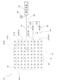
- composition of a die bonding device incorporating a suction stage of an embodiment It is a perspective view of the adsorption
- the die bonding apparatus 100 includes a pickup unit 10, an intermediate positioning unit 18, and a bonding unit 70.
- the pickup unit 10 is a portion that picks up the semiconductor die 13 from the surface of the wafer 12 and transports it to the intermediate positioning unit 18.
- the pickup unit 10 includes a wafer holder 11 for holding the wafer 12, a push-up mechanism 16 for pushing up the semiconductor die 13 from below, and a collet 15 for picking up the semiconductor die 13 pushed up by the push-up mechanism 16.
- a pickup head 14 is provided. When the semiconductor die 13 is adsorbed to the collet 15, the pickup head 14 transfers the semiconductor die 13 from the pickup unit 10 to the intermediate positioning unit 18 and places the semiconductor die 13 on the surface 21 a of the adsorption stage 20.
- the intermediate positioning unit 18 is a suction stage 20 for temporarily holding the semiconductor die 13 on the surface 21 a, and a camera for positioning the semiconductor die 13 held on the surface 21 a by suction and disposed on the surface 21 a of the suction stage 20. It has 48 and.
- the suction stage 20 is composed of an upper plate 21 and a valve unit 50.
- the bonding unit 70 includes a bonding stage 71 that vacuum-sucks the substrate 17 to the surface, and a bonding head 72 including a bonding tool 73 that picks up the semiconductor die 13 from the surface 21 a of the suction stage 20 and bonds it onto the substrate 17. There is.
- the adsorption stage 20 has an upper plate 21 provided with a large number of adsorption holes 22 equally provided on the surface 21a, and first and second check valves 61, 62 shown in FIGS. And a valve unit 50 for containing the same.
- the suction holes 22 include a first group A1 formed by the suction holes 22 at the central portion, a third group A3 formed by the suction holes 22 at the outermost periphery, a first group A1 and a first group A1. It is divided into three groups of 2nd group A2 comprised by the adsorption hole 22 located in the middle with 3 group A3. The grouping of the suction holes 22 will be described in detail later.
- a recess 23 and step portions 29 and 31 following the recess 23 are provided on the lower surface 21 b side which is a surface opposite to the surface 21 a of the upper plate 21, a recess 23 and step portions 29 and 31 following the recess 23 are provided on the lower surface 21 b side which is a surface opposite to the surface 21 a of the upper plate 21, a recess 23 and step portions 29 and 31 following the recess 23 are provided on the recess 23 has a size surrounding the outside of the array of the suction holes 22 as shown by a broken line in FIG.
- Two annular projections 24 and 25 project from the bottom surface 23 a of the recess 23.
- the annular convex portion 24 constitutes an annular third cavity 28 surrounded by the side surface and the bottom surface 23 a of the concave portion 23.
- the convex portions 24 and 25 constitute an annular second cavity 27 surrounded by the inner peripheral surface of the annular convex portion 24 and the outer peripheral surface of the convex portion 25.
- the suction holes 22 included in the first group A1 communicate with the first cavity 26, and the suction holes 22 included in the second group A2 communicate with the second cavity 27, and the third group A3
- the adsorption holes 22 included in A3 communicate with the third cavity 28.
- the convex portions 24 and 25 are also walls which divide the suction holes 22 into the first, second and third groups A1, A2 and A3.
- An upper packing 29 a is fitted in the step 29 following the recess 23, and a spacer 30 a and a lower packing 31 a are fitted in the step 30 following the step 29.
- the upper surface of the upper packing 29 a constitutes the lower surface of the first, second and third cavities 26, 27 and 28.
- the upper packing 29a, the spacer 30a, and the lower packing 31a are provided with through holes 33, 36, 39 at a first position, and are provided with through holes 34, 37, 39 at a second position. Holes 32, 35, 38 are provided.
- the through holes 33, 36, 39 provided at the first position constitute a first vacuum channel 41 communicating with the first cavity 26, and the through holes 34, 37, 40 provided at the second position are a second cavity
- the through holes 32, 35, 38 provided at the third position constitute the third vacuum flow passage 43 communicating with the third cavity 28.
- the first vacuum flow channel 41 is connected to the through hole 52 provided in the base 51 of the valve unit 50.
- the second and third vacuum flow channels 42 and 43 are in communication with the first and second valve housing recesses 55 a and 55 b of the base 51.
- through holes 53a and 53b are provided on the bottom surfaces of the first and second valve housing concave portions 55a and 55b, respectively.
- the through holes 52, 53a, 53b are connected to the vacuum device 45 through the pipe 54.
- the pipe 54 is provided with a pressure sensor 46 for detecting the pressure of the pipe.
- the first check valve 61 is accommodated in the first valve accommodating recess 55 a communicating with the second vacuum passage 42 and the through hole 53 a, and the third vacuum passage 43 is accommodated.
- a second check valve 62 is accommodated in the second valve accommodation recess 55b in communication with the through hole 53b.
- the first check valve 61 is disposed in a direction to block the flow of air from the suction holes 22 included in the second group A2 to the vacuum device 45.
- the first and second check valves 61 and 62 have the same structure.
- the first and second check valves 61 and 62 have a substantially rectangular parallelepiped main body 63 having a circular arc-shaped valve seat surface 64 provided with a hole 66 through which air flows, and a valve seat And a strip-shaped valve body 65 formed of an elastic body attached to one end of the surface 64.
- the valve seat surface 64 is roughened, and for example, the arithmetic mean roughness Ra may be about 1.6.
- the valve body 65 is a metal plate whose surface is smooth.
- the hole 66 is in communication with the hole 69 provided on the side surface of the main body 63 by flow paths 67 and 68 provided inside the main body.
- the holes 69 provided on the side surfaces of the main body 63 are through holes 53a. , 53 b to the vacuum device 45.
- the gap D between the tip of the valve body 65 on the hole 66 side and the wall surfaces of the first and second valve housing concave portions 55a and 55b communicates with the second and third vacuum channels 42 and 43.
- the valve body 65 When the hole 69 is evacuated by the vacuum device 45 connected to the hole 69, the valve body 65 adsorbs to the valve seat surface 64 in the hole 66 and seals the hole 66, as shown by the arrow 95 in FIG. As a result, the first and second check valves 61 and 62 are closed. In addition, when the hole 69 reaches the atmospheric pressure, the valve body 65 is separated from the valve seat surface 64 by its own elastic force to open the hole 66, and the first and second check valves 61 and 62 are closed. However, since the valve seat surface 64 is rough, even if the first and second check valves 61 and 62 are closed, minute air leaks between the valve seat surface 64 and the valve body 65. Occur.
- the pressure sensor 46 at the inlet of the vacuum device 45 is a pressure higher than -60 to -70 Pa, for example, about -10 Pa, which is an ultimate pressure when the semiconductor die 13 is adsorbed to the surface 21a. .
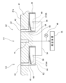
- the semiconductor die 13a having a small size has the same size as the broken line indicating the outer periphery of the first group A1 shown in FIG. 4 and covers the surface of the suction hole 22 included in the first group A1, and the second and third groups A2.
- A3 has a size that does not overlap the suction holes 22.
- the small-sized semiconductor die 13a when the small-sized semiconductor die 13a is placed on the surface 21a, the surface of the suction hole 22 included in the first group A1 is covered. As a result, the first vacuum flow channel 41 is evacuated and the semiconductor die 13a is attracted to the surface 21a. Since the suction holes 22 are uniformly arranged, the semiconductor die 13a is vacuum-held on the surface 21a in a well-balanced manner as a whole. Since the second and third vacuum channels 42 and 43 are closed by the first and second check valves 61 and 62, the air contained in the first vacuum channel 41 is sucked by the vacuum device 45.
- the pressure of the first vacuum channel 41 reaches ⁇ 60 to ⁇ 70 Pa, which is the ultimate pressure when the semiconductor die 13 is adsorbed to the surface 21 a.
- the pressure sensor 46 provided at the inlet pressure of the vacuum device 45 also detects the pressure of -60 to -70 Pa, and the control device (not shown) detects that the semiconductor die 13a is held by suction. Then, the control device obtains an image of the semiconductor die 13a by the camera 48 and performs position detection.
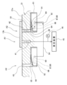
- the medium-sized semiconductor die 13b has the same size as the broken line indicating the outer periphery of the second group A2 shown in FIG. 4, and covers the surface of the adsorption holes 22 included in the first and second groups A1 and A2. is there. However, the suction holes 22 included in the area of the third group A3 do not overlap.
- the first and second check valves 61 and 62 are closed in a state where the vacuum device 45 is activated before the semiconductor die 13 is adsorbed. 2.
- the third vacuum flow channels 42 and 43 are closed, and the first vacuum flow channel 41 is open to the atmosphere, and air flows from the first vacuum flow channel 41 toward the vacuum device 45.
- the inlet pressure of the vacuum device 45 is, for example, about -10 Pa.
- the semiconductor die 13b covers the surfaces of the suction holes 22 included in the first and second groups A1 and A2.
- the first vacuum channel 41 is evacuated, and the central portion of the semiconductor die 13b is attracted to the surface 21a. Since the first check valve 61 is in a closed state and there is a slight leak of air, when the second vacuum flow channel 42 is covered by the semiconductor die 13 b, the air contained in the second vacuum flow channel 42 is shown in FIG. As indicated by the arrow 92 of FIG. 9, the fluid flows into the vacuum device 45 through the first check valve 61. For this reason, the pressure in the second vacuum channel 42 gradually decreases toward the vacuum.
- the second vacuum flow channel 42 is in the same vacuum state as the first vacuum flow channel 41, and the peripheral portion of the semiconductor die 13b is adsorbed to the surface 21a. Since the suction holes 22 are evenly arranged, the semiconductor die 13b is vacuum-held on the surface 21a in a well-balanced manner by the suction holes 22 included in the first group A1 and the suction holes 22 included in the second group A2. Ru.
- the third vacuum flow channel 43 is closed by the second check valve 62, it has entered the first and second vacuum flow channels 41 and 42.
- the pressure of the first and second vacuum channels 41, 42 reaches -60 to -70 Pa, which is the ultimate pressure when the semiconductor die 13b is adsorbed to the surface 21a.
- the pressure sensor 46 provided at the inlet pressure of the vacuum device 45 also detects the pressure of -60 to -70 Pa, and the control device (not shown) detects that the semiconductor die 13b is held by suction. Then, the control device obtains an image of the semiconductor die 13 b by the camera 48 and performs position detection.
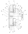
- the large-sized semiconductor die 13c is sized to cover all the suction holes 22 shown in FIG.
- the semiconductor die 13c covers the surfaces of all the suction holes 22.
- the first vacuum channel 41 is evacuated, and the semiconductor die 13c is attracted to the surface 21a.
- the first and second check valves 61 and 62 are in the closed state, there is a minute leak of air, and therefore the second and third vacuum channels 42 and 43 are covered by the semiconductor die 13c as described above. , And the first and second check valves 61 and 62 are opened.
- the second and third vacuum channels 42 and 43 are in the same vacuum state as the first vacuum channel 41, and the peripheral portion of the semiconductor die 13c is attracted to the surface 21a. Since the suction holes 22 are evenly arranged, the semiconductor die 13c is vacuum-held on the surface 21a in a well-balanced manner by the suction holes 22 included in the first to third groups A1 to A3.
- the pressure of the first, second and third vacuum channels 41, 42 and 43 is obtained. Reaches an ultimate pressure of -60 to -70 Pa when the semiconductor die 13c is adsorbed to the surface 21a.
- the pressure sensor 46 provided at the inlet pressure of the vacuum device 45 also detects a pressure of -60 to -70 Pa, and a control device (not shown) detects that the semiconductor die 13c is adsorbed and fixed. Then, the control device acquires an image of the semiconductor die 13 c by the camera 48 and performs position detection.
- the suction stage 20 divides the plurality of suction holes 22 into the first to third groups A1 to A3 according to the size of the semiconductor die 13, and the first to third groups A1 to A3.
- the first to third vacuum channels 41 to 43 connecting the plurality of suction holes 22 to the vacuum device 45 are provided in each case, and the suction holes 22 are open to the atmosphere in the second and third vacuum channels 42 and 43
- the first and second check valves 61 and 62 are provided which are closed when the semiconductor die 13 closes the suction holes 22.
- the suction holes 22 are evenly arranged. As a result, regardless of the size of the semiconductor die 13, the semiconductor die 13 can be uniformly adsorbed and held by the suction holes 22 in a well-balanced manner. Then, the position of the semiconductor die 13 can be suitably detected using the camera 48.
- the suction holes 22 closed by the semiconductor die 13 are evacuated according to the size of the semiconductor die 13 and the other suction holes 22 are shut off from the vacuum device 45. Therefore, regardless of the size of the semiconductor die 13, the vacuum pressure at the time of vacuum-adsorbing the semiconductor die 13 can be a pressure at which the adsorption and retention of the semiconductor die 13 can be determined. The adsorption retention can be confirmed.
- the suction stage 20 can preferably hold a plurality of semiconductor dies 13 of a plurality of sizes by one suction stage 20 without exchanging the suction stage 20 according to the size of the semiconductor die.
- the tact time of bonding can be shortened, and efficient bonding can be performed.
- the first vacuum flow channel 41 is described as not having a check valve, but the present invention is not limited to this, and a check valve having a structure similar to that of the first check valve 61 may be provided. It is also good.
- the check valve may be provided outside without being incorporated into the adsorption stage 20. In this case, other types of check valves, such as, for example, a swing check valve may be used.
Landscapes
- Container, Conveyance, Adherence, Positioning, Of Wafer (AREA)
- Wire Bonding (AREA)
- Die Bonding (AREA)
Abstract
Description
Claims (4)
- 異なるサイズの半導体ダイを吸着保持する吸着ステージであって、
複数の吸着孔が設けられた上板と、
前記上板に設けられた複数の前記吸着孔を半導体ダイのサイズに応じた複数のグループ毎に真空装置に接続する複数の真空流路と、
複数の前記真空流路の内の少なくとも1つの前記真空流路に設けられた逆止弁と、を含み、
前記逆止弁は、前記吸着孔が大気開放されている場合に閉となり、半導体ダイによって前記吸着孔が塞がれると開となること、
を特徴とする吸着ステージ。 - 請求項1に記載の吸着ステージであって、
前記逆止弁は、弁座面が粗面であり、閉状態において弁体と前記弁座面との間から空気の微小リークが発生する弁であること、
を特徴とする吸着ステージ。 - 請求項2に記載の吸着ステージであって、
前記弁座面は空気が通流する孔が設けられた円弧面状の面であり、前記弁体は前記弁座面の一端に取り付けられた弾性体で構成された帯状体であり、前記逆止弁は、前記孔を前記弁体が開閉する弁であること、
を特徴とする吸着ステージ。 - 請求項1から3のいずれか1項に記載の吸着ステージであって、
前記吸着孔が均等に配置されていること、
を特徴とする吸着ステージ。
Priority Applications (4)
| Application Number | Priority Date | Filing Date | Title |
|---|---|---|---|
| JP2019544980A JP6817658B2 (ja) | 2017-09-28 | 2018-09-18 | 吸着ステージ |
| CN201880062674.0A CN111149197B (zh) | 2017-09-28 | 2018-09-18 | 吸附平台 |
| KR1020207011459A KR102339079B1 (ko) | 2017-09-28 | 2018-09-18 | 흡착 스테이지 |
| SG11202004896TA SG11202004896TA (en) | 2017-09-28 | 2018-09-18 | Suction stage |
Applications Claiming Priority (2)
| Application Number | Priority Date | Filing Date | Title |
|---|---|---|---|
| JP2017188635 | 2017-09-28 | ||
| JP2017-188635 | 2017-09-28 |
Publications (1)
| Publication Number | Publication Date |
|---|---|
| WO2019065355A1 true WO2019065355A1 (ja) | 2019-04-04 |
Family
ID=65901325
Family Applications (1)
| Application Number | Title | Priority Date | Filing Date |
|---|---|---|---|
| PCT/JP2018/034388 Ceased WO2019065355A1 (ja) | 2017-09-28 | 2018-09-18 | 吸着ステージ |
Country Status (6)
| Country | Link |
|---|---|
| JP (1) | JP6817658B2 (ja) |
| KR (1) | KR102339079B1 (ja) |
| CN (1) | CN111149197B (ja) |
| SG (1) | SG11202004896TA (ja) |
| TW (1) | TWI684223B (ja) |
| WO (1) | WO2019065355A1 (ja) |
Cited By (2)
| Publication number | Priority date | Publication date | Assignee | Title |
|---|---|---|---|---|
| KR20210123194A (ko) * | 2020-04-01 | 2021-10-13 | 삼성디스플레이 주식회사 | 표시 장치의 제조 장치 및 표시 장치의 제조 방법 |
| CN114939852A (zh) * | 2022-06-06 | 2022-08-26 | 深圳宜美智科技股份有限公司 | 高精度可移动真空吸附平台及高精度检测设备 |
Families Citing this family (4)
| Publication number | Priority date | Publication date | Assignee | Title |
|---|---|---|---|---|
| JP7630956B2 (ja) * | 2020-10-30 | 2025-02-18 | 三星電子株式会社 | 半導体製造装置およびチップハンドリング方法 |
| KR102787801B1 (ko) * | 2020-11-24 | 2025-03-31 | 주식회사 기가레인 | 흡착 플레이트 |
| KR102630948B1 (ko) * | 2020-12-29 | 2024-01-30 | 세메스 주식회사 | 반도체 패키지 이송 방법과 반도체 패키지 이송 모듈 및 반도체 패키지 절단 및 분류 장치 |
| KR102893069B1 (ko) * | 2024-06-14 | 2025-12-01 | 양진석 | 다이 이송 장치 및 다이 이송 방법 |
Citations (6)
| Publication number | Priority date | Publication date | Assignee | Title |
|---|---|---|---|---|
| JPS618250A (ja) * | 1984-06-23 | 1986-01-14 | Mitsubishi Electric Corp | 真空吸着台 |
| JPH0490946U (ja) * | 1990-12-26 | 1992-08-07 | ||
| JPH081464A (ja) * | 1992-06-17 | 1996-01-09 | Shibayama Kikai Kk | ユニバーサルチャック機構の自動切換装置 |
| JP2009200377A (ja) * | 2008-02-25 | 2009-09-03 | Panasonic Corp | ダイボンディング装置 |
| JP2009212254A (ja) * | 2008-03-04 | 2009-09-17 | Toray Eng Co Ltd | チップ搭載方法およびチップ搭載装置 |
| JP2013179207A (ja) * | 2012-02-29 | 2013-09-09 | Hitachi High-Tech Instruments Co Ltd | 電子部品の載置テーブルと同テーブルを備えたダイボンダ |
Family Cites Families (8)
| Publication number | Priority date | Publication date | Assignee | Title |
|---|---|---|---|---|
| WO2007114331A1 (ja) * | 2006-04-04 | 2007-10-11 | Miraial Co., Ltd. | 薄板収納容器 |
| JP5126091B2 (ja) * | 2009-02-02 | 2013-01-23 | ウシオ電機株式会社 | ワークステージ及び該ワークステージを使用した露光装置 |
| TWI529829B (zh) * | 2011-05-27 | 2016-04-11 | 東麗工程股份有限公司 | Installation method and installation device |
| JP5815345B2 (ja) | 2011-09-16 | 2015-11-17 | ファスフォードテクノロジ株式会社 | ダイボンダ及びボンディング方法 |
| JP2013232466A (ja) * | 2012-04-27 | 2013-11-14 | Mitsuboshi Diamond Industrial Co Ltd | 基板吸着装置 |
| CN103904013B (zh) * | 2012-12-28 | 2016-12-28 | 上海微电子装备有限公司 | 一种真空吸附装置及吸附测校方法 |
| JP2015013737A (ja) * | 2013-07-08 | 2015-01-22 | 三菱電機株式会社 | ワーク吸着装置およびワーク吸着方法 |
| JP2016532282A (ja) * | 2013-09-26 | 2016-10-13 | ズス・マイクロテック・リソグラフィ・ゲゼルシャフト・ミット・ベシュレンクテル・ハフツングSuss MicroTec Lithography GmbH | ウエハを吸引し保持するためのチャック |
-
2018
- 2018-09-18 SG SG11202004896TA patent/SG11202004896TA/en unknown
- 2018-09-18 CN CN201880062674.0A patent/CN111149197B/zh active Active
- 2018-09-18 JP JP2019544980A patent/JP6817658B2/ja active Active
- 2018-09-18 WO PCT/JP2018/034388 patent/WO2019065355A1/ja not_active Ceased
- 2018-09-18 KR KR1020207011459A patent/KR102339079B1/ko active Active
- 2018-09-26 TW TW107133701A patent/TWI684223B/zh active
Patent Citations (6)
| Publication number | Priority date | Publication date | Assignee | Title |
|---|---|---|---|---|
| JPS618250A (ja) * | 1984-06-23 | 1986-01-14 | Mitsubishi Electric Corp | 真空吸着台 |
| JPH0490946U (ja) * | 1990-12-26 | 1992-08-07 | ||
| JPH081464A (ja) * | 1992-06-17 | 1996-01-09 | Shibayama Kikai Kk | ユニバーサルチャック機構の自動切換装置 |
| JP2009200377A (ja) * | 2008-02-25 | 2009-09-03 | Panasonic Corp | ダイボンディング装置 |
| JP2009212254A (ja) * | 2008-03-04 | 2009-09-17 | Toray Eng Co Ltd | チップ搭載方法およびチップ搭載装置 |
| JP2013179207A (ja) * | 2012-02-29 | 2013-09-09 | Hitachi High-Tech Instruments Co Ltd | 電子部品の載置テーブルと同テーブルを備えたダイボンダ |
Cited By (4)
| Publication number | Priority date | Publication date | Assignee | Title |
|---|---|---|---|---|
| KR20210123194A (ko) * | 2020-04-01 | 2021-10-13 | 삼성디스플레이 주식회사 | 표시 장치의 제조 장치 및 표시 장치의 제조 방법 |
| KR102788896B1 (ko) * | 2020-04-01 | 2025-04-02 | 삼성디스플레이 주식회사 | 표시 장치의 제조 장치 및 표시 장치의 제조 방법 |
| CN114939852A (zh) * | 2022-06-06 | 2022-08-26 | 深圳宜美智科技股份有限公司 | 高精度可移动真空吸附平台及高精度检测设备 |
| CN114939852B (zh) * | 2022-06-06 | 2023-02-24 | 深圳宜美智科技股份有限公司 | 高精度可移动真空吸附平台及高精度检测设备 |
Also Published As
| Publication number | Publication date |
|---|---|
| CN111149197B (zh) | 2023-06-02 |
| JPWO2019065355A1 (ja) | 2020-07-30 |
| KR20200051815A (ko) | 2020-05-13 |
| KR102339079B1 (ko) | 2021-12-14 |
| TW201921522A (zh) | 2019-06-01 |
| CN111149197A (zh) | 2020-05-12 |
| TWI684223B (zh) | 2020-02-01 |
| JP6817658B2 (ja) | 2021-01-27 |
| SG11202004896TA (en) | 2020-06-29 |
Similar Documents
| Publication | Publication Date | Title |
|---|---|---|
| JP6817658B2 (ja) | 吸着ステージ | |
| CN108136596A (zh) | 提供用于末端执行器的真空阀组件的系统和方法 | |
| CN108010876A (zh) | 用于拾取半导体器件的装置及其方法 | |
| CN108364903A (zh) | 用于末端执行器的吸附装置、末端执行器及其制造方法 | |
| JP2001267271A (ja) | 吸着装置 | |
| JP2015013737A (ja) | ワーク吸着装置およびワーク吸着方法 | |
| CN116469795A (zh) | 整平装置及整平方法 | |
| JP5316172B2 (ja) | ウェハ吸引パッド及びそれを備えたプリアライナ | |
| JP2014203967A (ja) | チャックテーブル | |
| JP2006319182A (ja) | 吸着保持装置 | |
| JP4797013B2 (ja) | 貼り合わせ装置 | |
| WO2020013013A1 (ja) | 搬送用ハンド | |
| JP2002137183A (ja) | 吸着パッド | |
| JPH0567551A (ja) | ウエハチヤツク | |
| JP2019100893A (ja) | リーク試験装置 | |
| TW201608668A (zh) | 承載裝置 | |
| JP6189727B2 (ja) | ユニバーサルチャック装置 | |
| TWM565701U (zh) | Workbench with ejection and adsorption function | |
| KR101597644B1 (ko) | 흡착 장치 | |
| WO2012014830A1 (ja) | 圧力検出装置 | |
| JP2005135958A (ja) | 真空ピンセット | |
| TWI913147B (zh) | 彈性開閉逆止吸盤 | |
| TW201616591A (zh) | 處理半導體封裝體的裝置及用該裝置取得其位置資訊的方法 | |
| CN206767101U (zh) | 一种多路吸附装置 | |
| TWI613449B (zh) | 吸附式測試裝置 |
Legal Events
| Date | Code | Title | Description |
|---|---|---|---|
| 121 | Ep: the epo has been informed by wipo that ep was designated in this application |
Ref document number: 18860106 Country of ref document: EP Kind code of ref document: A1 |
|
| DPE1 | Request for preliminary examination filed after expiration of 19th month from priority date (pct application filed from 20040101) | ||
| ENP | Entry into the national phase |
Ref document number: 2019544980 Country of ref document: JP Kind code of ref document: A |
|
| NENP | Non-entry into the national phase |
Ref country code: DE |
|
| ENP | Entry into the national phase |
Ref document number: 20207011459 Country of ref document: KR Kind code of ref document: A |
|
| 122 | Ep: pct application non-entry in european phase |
Ref document number: 18860106 Country of ref document: EP Kind code of ref document: A1 |