WO2018207403A1 - トランス装置 - Google Patents
トランス装置 Download PDFInfo
- Publication number
- WO2018207403A1 WO2018207403A1 PCT/JP2017/047174 JP2017047174W WO2018207403A1 WO 2018207403 A1 WO2018207403 A1 WO 2018207403A1 JP 2017047174 W JP2017047174 W JP 2017047174W WO 2018207403 A1 WO2018207403 A1 WO 2018207403A1
- Authority
- WO
- WIPO (PCT)
- Prior art keywords
- winding
- primary
- wiring
- circuit
- secondary winding
- Prior art date
- Legal status (The legal status is an assumption and is not a legal conclusion. Google has not performed a legal analysis and makes no representation as to the accuracy of the status listed.)
- Ceased
Links
Images


Classifications
-
- H—ELECTRICITY
- H01—ELECTRIC ELEMENTS
- H01F—MAGNETS; INDUCTANCES; TRANSFORMERS; SELECTION OF MATERIALS FOR THEIR MAGNETIC PROPERTIES
- H01F27/00—Details of transformers or inductances, in general
- H01F27/28—Coils; Windings; Conductive connections
- H01F27/30—Fastening or clamping coils, windings, or parts thereof together; Fastening or mounting coils or windings on core, casing, or other support
- H01F27/306—Fastening or mounting coils or windings on core, casing or other support
-
- H—ELECTRICITY
- H01—ELECTRIC ELEMENTS
- H01F—MAGNETS; INDUCTANCES; TRANSFORMERS; SELECTION OF MATERIALS FOR THEIR MAGNETIC PROPERTIES
- H01F27/00—Details of transformers or inductances, in general
- H01F27/28—Coils; Windings; Conductive connections
- H01F27/2823—Wires
- H01F27/2828—Construction of conductive connections, of leads
-
- H—ELECTRICITY
- H01—ELECTRIC ELEMENTS
- H01F—MAGNETS; INDUCTANCES; TRANSFORMERS; SELECTION OF MATERIALS FOR THEIR MAGNETIC PROPERTIES
- H01F27/00—Details of transformers or inductances, in general
- H01F27/28—Coils; Windings; Conductive connections
-
- H—ELECTRICITY
- H01—ELECTRIC ELEMENTS
- H01F—MAGNETS; INDUCTANCES; TRANSFORMERS; SELECTION OF MATERIALS FOR THEIR MAGNETIC PROPERTIES
- H01F27/00—Details of transformers or inductances, in general
- H01F27/28—Coils; Windings; Conductive connections
- H01F27/2804—Printed windings
-
- H—ELECTRICITY
- H01—ELECTRIC ELEMENTS
- H01F—MAGNETS; INDUCTANCES; TRANSFORMERS; SELECTION OF MATERIALS FOR THEIR MAGNETIC PROPERTIES
- H01F27/00—Details of transformers or inductances, in general
- H01F27/28—Coils; Windings; Conductive connections
- H01F27/2847—Sheets; Strips
-
- H—ELECTRICITY
- H01—ELECTRIC ELEMENTS
- H01F—MAGNETS; INDUCTANCES; TRANSFORMERS; SELECTION OF MATERIALS FOR THEIR MAGNETIC PROPERTIES
- H01F27/00—Details of transformers or inductances, in general
- H01F27/28—Coils; Windings; Conductive connections
- H01F27/30—Fastening or clamping coils, windings, or parts thereof together; Fastening or mounting coils or windings on core, casing, or other support
-
- H—ELECTRICITY
- H01—ELECTRIC ELEMENTS
- H01F—MAGNETS; INDUCTANCES; TRANSFORMERS; SELECTION OF MATERIALS FOR THEIR MAGNETIC PROPERTIES
- H01F27/00—Details of transformers or inductances, in general
- H01F27/28—Coils; Windings; Conductive connections
- H01F27/32—Insulating of coils, windings, or parts thereof
- H01F27/324—Insulation between coil and core, between different winding sections, around the coil; Other insulation structures
- H01F27/325—Coil bobbins
-
- H—ELECTRICITY
- H01—ELECTRIC ELEMENTS
- H01F—MAGNETS; INDUCTANCES; TRANSFORMERS; SELECTION OF MATERIALS FOR THEIR MAGNETIC PROPERTIES
- H01F27/00—Details of transformers or inductances, in general
- H01F27/40—Structural association with built-in electric component, e.g. fuse
-
- H—ELECTRICITY
- H01—ELECTRIC ELEMENTS
- H01F—MAGNETS; INDUCTANCES; TRANSFORMERS; SELECTION OF MATERIALS FOR THEIR MAGNETIC PROPERTIES
- H01F30/00—Fixed transformers not covered by group H01F19/00
- H01F30/06—Fixed transformers not covered by group H01F19/00 characterised by the structure
- H01F30/10—Single-phase transformers
-
- H—ELECTRICITY
- H01—ELECTRIC ELEMENTS
- H01F—MAGNETS; INDUCTANCES; TRANSFORMERS; SELECTION OF MATERIALS FOR THEIR MAGNETIC PROPERTIES
- H01F38/00—Adaptations of transformers or inductances for specific applications or functions
- H01F38/08—High-leakage transformers or inductances
-
- H—ELECTRICITY
- H02—GENERATION; CONVERSION OR DISTRIBUTION OF ELECTRIC POWER
- H02M—APPARATUS FOR CONVERSION BETWEEN AC AND AC, BETWEEN AC AND DC, OR BETWEEN DC AND DC, AND FOR USE WITH MAINS OR SIMILAR POWER SUPPLY SYSTEMS; CONVERSION OF DC OR AC INPUT POWER INTO SURGE OUTPUT POWER; CONTROL OR REGULATION THEREOF
- H02M3/00—Conversion of DC power input into DC power output
- H02M3/22—Conversion of DC power input into DC power output with intermediate conversion into AC
- H02M3/24—Conversion of DC power input into DC power output with intermediate conversion into AC by static converters
- H02M3/28—Conversion of DC power input into DC power output with intermediate conversion into AC by static converters using discharge tubes with control electrode or semiconductor devices with control electrode to produce the intermediate AC
Definitions
- the present invention relates to a transformer device.
- the transformer device includes, for example, a transformer having a primary winding and a secondary winding, a primary circuit connected to the primary winding via a first wiring, and a secondary winding via a second wiring.
- a secondary circuit to be connected for example, Patent Document 1.
- the conventional transformer device may cause structural waste depending on the arrangement of the first and second wirings and the primary and secondary circuits, and there is room for further improvement in this respect.
- the present invention has been made in view of the above, and an object thereof is to provide a transformer device that can suppress structural waste.
- a transformer device is provided with a primary winding formed by winding a first conductor, and facing the primary winding.
- a transformer having a secondary winding formed by winding a second conductor, a first wiring connected to the primary winding and drawn to one side, and the first winding connected to the secondary winding.
- a second wiring drawn out to the same side as the wiring, and a base material provided on a side from which the first wiring and the second wiring are drawn out are provided.
- a secondary circuit connected to a winding, and the primary circuit and the secondary circuit are provided side by side along a crossing direction that intersects a lead-out direction from which the first wiring and the second wiring are drawn out. It is preferred that
- the primary winding has a leakage inductor that does not contribute to a transforming action, and the leakage inductor is provided on the primary circuit side in the crossing direction.
- the primary winding includes a flat and linear first conductor of a coil axis, and a leakage inductor axis positioned on the primary circuit side in the intersecting direction with respect to the coil axis.
- the secondary winding is formed by winding the plate-like and linear second conductor around the coil axis, and the primary winding and the second winding are wound around both axes.
- the secondary winding is preferably laminated along the coil axis direction, which is the direction along the coil axis.
- the primary winding and the secondary winding are provided, and a magnetic member including a magnetic material is provided, and the magnetic member is provided in an annular shape around the coil axis.
- a wall that surrounds the outer periphery of the secondary winding, the wall being open at the primary circuit and the secondary circuit side, and an opening angle around the coil axis is 120 ° to 180 °.
- it has an opening through which the leakage inductor and the terminal of the secondary winding are exposed.
- the transformer device includes a primary winding and a secondary winding, a first wiring connected to the primary winding and drawn to one side, and connected to the secondary winding on the same side as the first wiring. And a second wiring to be drawn out.
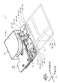
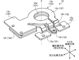
- FIG. 1 is a perspective view illustrating a configuration example of a transformer device according to an embodiment.
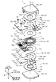
- FIG. 2 is an exploded perspective view illustrating a configuration example of the transformer device according to the embodiment.
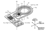
- FIG. 3 is a perspective view illustrating a configuration example on the surface side of the primary winding according to the embodiment.
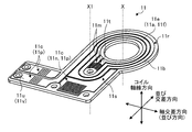
- FIG. 4 is a perspective view illustrating a configuration example on the back surface side of the primary winding according to the embodiment.
- FIG. 5 is a perspective view illustrating a configuration example of the secondary winding according to the embodiment.
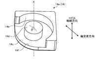
- FIG. 6 is a perspective view illustrating a configuration example of the first ferrite according to the embodiment.
- FIG. 7 is a schematic diagram illustrating a configuration example of the transformer device according to the embodiment.
- FIG. 8 is a schematic diagram illustrating a configuration example of a transformer device according to a comparative example.
- the transformer device 1 is a device that transforms a voltage.
- the transformer device 1 is a thin transformer device for a DC / DC converter, for example, and outputs a large current by stepping down.
- the transformer device 1 includes a transformer 10, first and second wirings 21 and 22, a base material 30, a primary circuit 41, a secondary circuit 42, and a control circuit 43.
- the circuit part 40 which has this.
- the coil axis direction is a direction along the coil axis X.
- the axis crossing direction is a direction crossing the coil axis direction, and is typically a direction orthogonal to the coil axis direction.
- the arrangement direction is a direction in which the transformer 10 and the circuit unit 40 are arranged.
- the arrangement crossing direction is a direction intersecting the arrangement direction, and is typically a direction orthogonal to the arrangement direction.
- the transformer 10 is a transformer that transforms voltage.
- the transformer 10 includes a primary winding part 11, a secondary winding part 12, a bobbin 13, and a ferrite 14.
- the primary winding portion 11 includes a primary winding 11a, an insulating plate-like insulating plate 11b, and a cooling via 11c.
- the insulating plate 11b is a four-layer substrate and is composed of a first layer to a fourth layer. In the insulating plate 11b, the first layer and the fourth layer constitute the surface layer, and the second layer and the third layer constitute the inner layer.
- the primary winding 11a is insulated from the front side primary winding 11d provided on the surface of the first layer of the insulating plate 11b and the back side primary winding 11e provided on the back surface of the fourth layer of the insulating plate 11b. It has inner layer side primary windings (not shown) provided on the mounting surfaces of the second and third layers of the plate 11b.
- the front-side primary winding 11d is a coil formed by winding a flat and linear first conductor 11f around the coil axis X and the leakage inductor axis X1 in a spiral shape along the axis crossing direction.
- the front primary winding 11d is a non-circular spiral coil formed so that the first conductor 11f goes around both the coil axis X and the leakage inductor axis X1.
- the front primary winding 11d may be formed as a conductor pattern on the surface of the insulating plate 11b by etching, or a conductor pattern formed by punching the conductor plate may be provided on the surface of the insulating plate 11b.
- the leakage inductor axis X1 extends in the same direction as the coil axis X, and is an axis lined with the coil axis X and positioned on the primary circuit 41 side in the intersecting direction.
- the front-side primary winding 11d includes a coil winding portion 11g that contributes to the transformation action, a leakage inductor 11h that does not contribute to the transformation action, a winding start end portion 11i that is an end portion on the winding start side, and an end on the winding end side And a winding end portion 11j which is a portion.
- the coil winding portion 11g is a portion provided around the coil axis X. When viewed from the coil axis direction, the coil winding portion 11g overlaps a secondary winding 12a described later, and is formed in a circular shape.
- the leakage inductor 11h is an inductor for resonance, and is a portion provided around the leakage inductor axis X1.
- the leakage inductor 11h is a portion that does not overlap the secondary winding 12a when viewed from the coil axis direction, and is formed in a non-circular shape.
- the leakage inductor 11h is provided on the primary circuit 41 side in the side-by-side crossing direction (crossing direction). That is, the leakage inductor 11h is provided so as to protrude from the coil winding portion 11g to the primary circuit 41 side along the intersecting direction.
- the first conductor 11f is wound along the axis crossing direction from the inside to the outside of the front side primary winding 11d, and the winding start end portion 11i is the front side primary winding.
- 11d is located on the outer peripheral side
- the winding end portion 11j is located on the inner peripheral side of the front primary winding 11d.
- the winding start end portion 11i constitutes a terminal 11k and is located on the primary circuit 41 side in the arrangement direction.
- the back side primary winding 11e has the same shape as the front side primary winding 11d, and is laminated on the front side primary winding 11d along the coil axis direction with an insulating plate 11b interposed.
- the back side primary winding 11e is a coil formed by spirally winding a flat and linear first conductor 11f around the coil axis X and the leakage inductor axis X1 along the axis crossing direction. That is, the back side primary winding 11e is a non-circular spiral coil formed so that the first conductor 11f goes around both the coil axis X and the leakage inductor axis X1.
- the back-side primary winding 11e may be formed as a conductor pattern on the back surface of the insulating plate 11b by etching, or a conductor pattern formed by punching the conductor plate may be provided on the back surface of the insulating plate 11b.
- the back side primary winding 11e includes a coil winding portion 11r that contributes to the transformation action, a leakage inductor 11s that does not contribute to the transformation action, a winding start end portion 11t that is an end portion on the winding start side, and an end on the winding end side And a winding end portion 11u.
- the coil winding portion 11r is a portion provided around the coil axis X. When viewed from the coil axis direction, the coil winding portion 11r is a portion that overlaps the secondary winding 12a and is formed in a circular shape.
- the leakage inductor 11s is a portion provided around the leakage inductor axis X1.
- the leakage inductor 11s is a portion that does not overlap the secondary winding 12a when viewed from the coil axis direction, and is formed in a non-circular shape.
- the leakage inductor 11s is provided on the primary circuit 41 side in the side-by-side crossing direction (crossing direction). In other words, the leakage inductor 11s is provided so as to protrude from the coil winding portion 11r to the primary circuit 41 side along the intersecting direction.
- the first conductor 11f is wound along the axis crossing direction from the inside to the outside of the back side primary winding 11e, and the winding start end portion 11t is the back side primary winding.
- the winding end portion 11u is located on the outer peripheral side of the back side primary winding 11e.
- the winding end portion 11u constitutes a terminal 11v and is located on the primary circuit 41 side in the arrangement direction.
- the inner layer and the surface layer are electrically connected by a through hole 11m, and the two inner layers are electrically connected by a cooling via 11c.
- the first layer front-side primary winding 11d and the second layer inner-layer side primary winding are electrically connected by the through hole 11m
- the second layer inner-layer side primary winding Are electrically connected to each other by a cooling via 11c
- the third layer inner primary winding and the fourth layer back primary winding 11e are through holes 11m.
- the primary winding 11a when an AC voltage is applied to the terminal 11k of the front side primary winding 11d and the terminal 11v of the back side primary winding 11e, a current flows through the primary winding 11a.
- the cooling via 11c cools the primary winding part 11.
- the cooling via 11c is provided with a plurality of through holes 11p penetrating the metal plate 11n and the insulating plate 11b along the coil axis direction in a state where the metal plate 11n is provided on the insulating plate 11b.
- the secondary winding part 12 is provided with the secondary winding 12a and the heat sink 12b, as shown in FIG.
- the secondary winding 12a is provided to face the primary winding 11a.
- the secondary winding 12a is configured with a smaller number of coil turns than the primary winding 11a.
- the secondary winding 12a is, for example, a two-turn (two-turn) coil, and includes an upper secondary winding 12c and a lower secondary winding 12d stacked on the upper secondary winding 12c in the coil axial direction.
- the upper secondary winding 12c is an annular member formed by winding a flat and linear second conductor 12e around the coil axis X along the axis crossing direction for one turn.
- the upper secondary winding 12c is an annular member formed so that the second conductor 12e goes around the coil axis X.
- the upper secondary winding 12c may be formed, for example, by punching a conductor plate or may be formed by winding a long plate-like member.
- the upper secondary winding 12c includes a coil winding portion 12f that contributes to the transformation action, a winding start end portion 12g that is an end portion on the winding start side, and a winding end end portion 12h that is an end portion on the winding end side.
- the coil winding portion 12f is a portion provided around the coil axis X.
- the coil winding portion 12f is a portion that overlaps with the coil winding portion 11g of the primary winding 11a when viewed from the coil axis direction, and is formed in a circular shape.
- the winding start end portion 12g constitutes the terminal 12i, and is positioned on the secondary circuit 42 side in the arrangement direction.
- the upper secondary winding 12c constitutes a connecting portion 12j in which the winding end portion 12h is connected to the lower secondary winding 12d, and is positioned on the secondary circuit 42 side in the arrangement direction.
- the lower secondary winding 12d has the same shape as the upper secondary winding 12c, and is laminated on the upper secondary winding 12c along the coil axis direction with the primary winding portion 11 interposed.
- the lower secondary winding 12 d and the upper secondary winding 12 c are insulated from the primary winding portion 11.
- a sheet-like upper insulating sheet 12 k that insulates the upper secondary winding 12 c and the primary winding portion 11 is provided between the upper secondary winding 12 c and the primary winding portion 11. (See FIG. 2).
- a sheet-like lower insulating sheet 12m that insulates the lower secondary winding 12d and the primary winding portion 11 is provided.
- the lower secondary winding 12d is an annular member formed by winding a flat and linear second conductor 12e around the coil axis X along the axis crossing direction for one turn. That is, the lower secondary winding 12d is an annular member formed so that the second conductor 12e goes around the coil axis X.
- the lower secondary winding 12d may be formed, for example, by punching a conductor plate or may be formed by winding a long plate member.
- the lower secondary winding 12d includes a coil winding portion 12n that contributes to the transformation action, a winding start end portion 12p that is an end portion on the winding start side, and a winding end end portion 12q that is an end portion on the winding end side.
- the coil winding portion 12n is a portion provided around the coil axis X.
- the coil winding portion 12n is a portion that overlaps with the coil winding portion 11g of the primary winding 11a when viewed from the coil axis direction, and is formed in a circular shape.
- the lower secondary winding 12d constitutes a connecting portion 12j in which the winding start end portion 12p is connected to the upper secondary winding 12c, and is located on the secondary circuit 42 side in the arrangement direction. Further, the lower secondary winding 12d has a winding end portion 12q constituting a terminal 12r and is located on the secondary circuit 42 side in the arrangement direction.
- the heat radiating plate 12b includes an upper heat radiating plate 12s provided in the coil winding portion 12f of the upper secondary winding 12c and a lower heat radiating plate 12t provided in the coil winding portion 12n of the lower secondary winding 12d.
- the upper heat radiating plate 12s is formed in a plate shape, extends from one end of the coil winding portion 12f of the upper secondary winding 12c, and extends in the intersecting direction.
- the upper heat radiating plate 12s radiates heat generated in the coil winding portion 12f of the upper secondary winding 12c.
- the lower heat radiating plate 12t is formed in a plate shape, extends from one end of the coil winding portion 12n of the lower secondary winding 12d, and extends in the intersecting direction.
- the lower heat radiating plate 12t radiates heat generated in the coil winding portion 12n of the lower secondary winding 12d.
- the bobbin 13 shown in FIG. 2 is a member that covers the coil winding portions 12f and 12n of the secondary winding 12a.
- the bobbin 13 includes an upper bobbin 13a covering the coil winding part 12f of the upper secondary winding 12c and a lower bobbin 13e covering the coil winding part 12n of the lower secondary winding 12d.
- the upper bobbin 13a includes an annular and plate-like annular member 13b extending in the axis crossing direction, a cylindrical tubular portion 13c extending from the inside of the annular member 13b in the coil axial direction, and an upper secondary of the annular member 13b. And a protruding portion 13d protruding toward the winding 12c.
- the annular member 13b covers the coil winding portion 12f of the upper secondary winding 12c when viewed from the coil axis direction.
- the cylindrical portion 13c is inserted inside the upper secondary winding 12c.
- the protruding portion 13d is fitted between one end portion in the circumferential direction of the upper secondary winding 12c and the other end portion.
- the upper bobbin 13a is attached to the coil winding part 12f of the upper secondary winding 12c in a state where the coil winding part 12f of the upper secondary winding 12c is covered from the coil axial direction.
- the lower bobbin 13e has the same configuration as the upper bobbin 13a, and an annular and plate-like annular member 13f extending in the axis crossing direction, and a cylindrical tube extending in the coil axis direction from the inside of the annular member 13f.
- a portion 13g and a protruding portion 13h protruding toward the lower secondary winding 12d of the annular member 13f are provided.
- the annular member 13f covers the coil winding portion 12n of the lower secondary winding 12d when viewed from the coil axis direction.
- the cylindrical portion 13g is inserted inside the lower secondary winding 12d.
- the protruding portion 13h is fitted between one end portion and the other end portion in the circumferential direction of the lower secondary winding 12d. Accordingly, the lower bobbin 13e is mounted on the coil winding portion 12n of the lower secondary winding 12d in a state where the coil winding portion 12n of the lower secondary winding 12d is covered from the coil axial direction.
- the ferrite 14 shown in FIG. 2 is a magnetic member that suppresses the loss of magnetic force through the magnetic force (magnetic flux) generated by the primary winding 11a and the secondary winding 12a.
- the ferrite 14 is a member containing a magnetic material, for example, a composite oxide of iron oxide and metal.
- the ferrite 14 is provided with a primary winding 11a and a secondary winding 12a.
- An upper ferrite 14a provided on the upper secondary winding 12c side and a lower ferrite 14b provided on the lower secondary winding 12d side. With. As shown in FIG.
- the upper ferrite 14 a includes a fan-like and plate-like upper surface portion 14 c provided in the axis crossing direction, and the primary winding 11 a and the secondary winding along the coil axial direction from the center of the upper surface portion 14 c.
- a columnar magnetic core 14d extending to the side of 12a and inserted inside the primary winding 11a and the secondary winding 12a, and provided in a ring around the coil axis X, the primary windings 11a and 2
- the wall 14e has an opening 14f in which a primary circuit 41 and a secondary circuit 42 described later are opened.
- the magnetic core 14d is wound with a primary winding 11a and a secondary winding 12a.
- the opening 14f has an opening angle ⁇ of 120 ° to 180 ° centered on the coil axis X, and the leakage inductors 11h and 11s, the terminals 12i and 12r of the secondary winding 12a, and the connecting portion 12j are the openings 14f.
- the opening angle ⁇ is appropriately set depending on the sizes of the primary winding 11a and the secondary winding 12a. In the opening 14f, when the opening angle ⁇ is relatively small, leakage of magnetic force (magnetic flux) is reduced and noise is reduced.
- the opening 14f particularly when the opening angle ⁇ is larger than 180 °, leakage of magnetic force increases and noise increases. As described above, it is desirable that the opening 14f has a small opening angle ⁇ .
- the thickness of the second conductor 12e of the secondary winding 12a is determined by the current or the like. It is 180 degrees.
- the lower ferrite 14b is a fan-shaped and plate-shaped member, and extends along the axis crossing direction.
- the lower ferrite 14b is combined with the upper ferrite 14a in the coil axial direction.
- the ferrite 14 sandwiches the primary winding 11a and the secondary winding 12a between the upper ferrite 14a and the lower ferrite 14b along the coil axis direction.
- a plurality of bolts 51 to 53 are provided with a hole portion 12u of the upper secondary winding 12c, a hole portion 12v of the upper insulating sheet 12k, a hole portion 11w of the primary winding portion 11, and a lower insulating sheet 12m. Each member is fixed by being inserted and fastened into the hole 12w and the hole 12x of the lower secondary winding 12d.
- the first wiring 21 (21a, 21b) is connected to the primary winding 11a and drawn out to one side in the arrangement direction.
- the first wiring 21 a has one end connected to the terminal 11 k of the front primary winding 11 d and the other end connected to the primary circuit 41.
- the first wiring 21 b has one end connected to the terminal 11 v of the back side primary winding 11 e and the other end connected to the primary circuit 41.
- the second wiring 22 (22a to 22c) is connected to the secondary winding 12a and drawn to the same side as the first wiring 21.
- the second wiring 22 a has one end connected to the terminal 12 i of the upper secondary winding 12 c and the other end connected to the secondary circuit 42.
- the second wiring 22b has one end connected to the terminal 12r of the lower secondary winding 12d and the other end connected to the secondary circuit 42.
- the second wiring 22c has one end connected to a connecting portion (center tap) 12j between the upper secondary winding 12c and the lower secondary winding 12d, and the other end connected to the secondary circuit 42.
- the base material 30 is an insulating plate-like member, and is provided on the side from which the first wiring 21 and the second wiring 22 are drawn.
- the base materials 30 are arranged side by side on one side of the transformer 10 along the arrangement direction.
- the base material 30 is formed in a rectangular shape, for example.
- the base material 30 has, for example, short sides along the direction of alignment, and long sides aligned along the direction of intersection.
- the primary circuit 41 is a switching circuit having a plurality of switching elements, for example, and is provided on the base material 30.
- the primary circuit 41 is disposed on the base material 30 so as to face the terminals 11k and 11v of the primary winding 11a in the alignment direction.
- the primary circuit 41 is connected to a DC power source and a primary winding 11a (not shown), converts DC power output from the DC power source into AC power, and outputs the converted AC power to the primary winding 11a.
- the primary circuit 41 is mounted on the base material 30 along with the secondary circuit 42 along the direction of crossing.
- the secondary circuit 42 is, for example, a synchronous rectification circuit and a smoothing circuit having a plurality of switching elements, and is provided on the base material 30.
- the secondary circuit 42 is arranged on the base material 30 so as to face the terminals 12i and 12r of the secondary winding 12a and the connecting portion (center tap) 12j in the alignment direction.
- the secondary circuit 42 is connected to the secondary winding 12a and a load (not shown), rectifies the AC power output from the secondary winding 12a, smoothes the rectified DC power, and outputs it to the load.
- the primary circuit 41 and the secondary circuit 42 are mounted on the base material 30 side by side along the crossing direction.
- the control circuit 43 is a circuit that controls the primary circuit 41 and the secondary circuit 42.
- the control circuit 43 is connected to the primary circuit 41 and controls on / off of each switching element of the switching circuit, for example.
- the control circuit 43 is connected to the secondary circuit 42 and controls, for example, on / off of each switching element of the synchronous rectification circuit.
- the transformer device 1 outputs DC power from the DC power source to the primary circuit 41, converts the DC power into AC power by the primary circuit 41, and outputs the AC power to the primary winding 11a. Then, the transformer device 1 supplies AC power stepped down to the secondary side by electromagnetic induction of the primary winding 11a and the secondary winding 12a, rectifies the AC power, and smoothes the rectified DC power. Supply to the load.
- the transformer device 1 according to the embodiment is compared with the transformer device 100 according to the comparative example.
- the transformer device 100 according to the comparative example has a base 110 formed in a U-shape, and has a notch 111 formed by notching the base 110.
- the transformer 120 is disposed in the notch 111 of the base 110
- the primary circuit 131 is disposed on one side of the base 110 with the transformer 120 interposed therebetween
- the secondary circuit is disposed on the other side of the base 110.
- 132 is arranged.
- the primary winding 121 and the primary circuit 131 are connected by the first wiring 141
- the secondary winding 122 and the secondary circuit 132 are connected by the second wiring 142.
- the first wirings 141 are arranged and led out to one side of the transformer 120 along the intersecting direction, and the second wirings 142 are arranged and led out to the other side of the transformer 120 along the intersecting direction.
- the primary circuit 131 and the secondary circuit 132 are connected to the control circuit 133.
- the transformer device 1 is opposed to the primary winding 11a formed by winding the first conductor 11f and the primary winding 11a.
- a transformer 10 having a secondary winding 12a formed by winding a second conductor 12e, a first wiring 21 connected to the primary winding 11a and drawn out to one side, and a secondary winding 12a
- the second wiring 22 connected to the first wiring 21 and drawn to the same side as the first wiring 21, the base material 30 provided on the side from which the first wiring 21 and the second wiring 22 are drawn, and the first wiring 21 provided on the base material 30.
- the first wiring 21 connected to the primary winding 11a and the second wiring 22 connected to the secondary winding 12a are drawn out to one side.
- the transformer 120 is provided in the notch portion 111 in which the base material 110 is partially cut out, and the first and second wirings 141 and 142 are drawn out from the transformer 120 on both sides.
- the notch 111 can be eliminated, and the discarded base material 112 can be suppressed.
- the transformer device 1 can suppress structural waste and can reduce manufacturing costs. Moreover, since the transformer device 1 can eliminate the processing of the notch 111, the processing of the substrate 30 can be facilitated. Moreover, since the transformer apparatus 1 can reduce the empty space in which the circuit is not formed in the base material 30 rather than the transformer apparatus 100 which concerns on a comparative example, it can suppress an enlargement.
- the primary circuit 41 and the secondary circuit 42 are provided side by side along the crossing direction that intersects the lead-out direction (alignment direction) from which the first wiring 21 and the second wiring 22 are drawn. It is done. Thereby, the transformer device 1 can arrange the primary circuit 41 so as to face the primary winding 11a, and can arrange the secondary circuit 42 so as to face the secondary winding 12a. Therefore, the transformer device 1 can relatively shorten the lengths of the first wiring 21 and the second wiring 22.
- the primary winding 11a includes the leakage inductors 11h and 11s that do not contribute to the transformation action, and the leakage inductors 11h and 11s are provided on the primary circuit 41 side in the crossing direction.
- the transformer device 1 can share the leakage inductors 11h and 11s as part of the portion connecting the coil winding portions 11g and 11r and the terminals 11k and 11v, thereby simplifying the circuit.
- the transformer device 1 uses the leakage inductors 11h and 11s, soft switching by the primary circuit 41 is facilitated and switching efficiency can be improved.
- the transformer device 1 can suppress an increase in size as compared with a case where a resonance inductor is added instead of the leakage inductors 11h and 11s. For example, when a resonance inductor is added, it is necessary to provide a certain interval in order to insulate the transformer inductor from the resonance inductor, which may increase the size.
- the primary winding 11 a is located on the side of the primary circuit 41 in the cross direction in which the flat and linear first conductor 11 f is aligned with the coil axis X and the coil axis X.
- the secondary winding 12a is formed by winding a flat and linear second conductor 12e around the coil axis X, and is formed by winding around both axes of the leakage inductor axis X1.
- the wire 11a and the secondary winding 12a are stacked along the coil axis direction, which is the direction along the coil axis X.
- the primary winding 11 a and the secondary winding 12 a are provided, and the ferrite 14 including the magnetic material is provided.
- the ferrite 14 is annularly provided around the coil axis X and the primary winding. 11a and a wall portion 14e surrounding the outer periphery of the secondary winding 12a.
- the wall portion 14e is opened on the primary circuit 41 and secondary circuit 42 side, and an opening angle ⁇ about the coil axis X is 120 ° to 120 °. It is 180 °, and has the openings 14f through which the leakage inductors 11h and 11s and the terminals 12i and 12r of the secondary winding 12a and the connecting portion (center tap) 12j are exposed.
- the transformer device 1 can suppress the opening angle ⁇ of the opening 14f while exposing the terminals 12i and 12r of the leakage inductors 11h and 11s and the secondary winding 12a and the connecting portion (center tap) 12j. . Therefore, the transformer device 1 can suppress leakage of magnetic force of the primary winding 11a and the secondary winding 12a, and can reduce noise.
- the transformer device 1 has been described as being the transformer 10 in which the thin primary winding 11a and the secondary winding 12a are laminated, the invention is not limited thereto.
- the transformer device 1 may be, for example, a transformer in which a spiral primary winding and a secondary winding are opposed to each other.
- the transformer device 1 may be provided with a magnetic core for leakage along the leakage inductor axis X1.
- the primary winding 11a is formed so that the first conductor 11f circulates both the magnetic core 14d along the coil axis X and the magnetic core for leakage along the leakage inductor axis X1. Is done.
Landscapes
- Engineering & Computer Science (AREA)
- Power Engineering (AREA)
- Coils Of Transformers For General Uses (AREA)
Abstract
第1導体が巻き回されて形成された1次巻線、及び、1次巻線に対向して設けられ第2導体が巻き回されて形成された2次巻線を有するトランス(10)と、1次巻線に接続され一方側に引き出される第1配線(21)と、2次巻線に接続され第1配線(21)と同じ側に引き出される第2配線(22)と、第1配線(21)及び第2配線(22)が引き出される側に設けられる基材(30)と、基材(30)に設けられ第1配線(21)を介して1次巻線に接続される1次回路(41)と、基材(30)に設けられ第2配線(22)を介して2次巻線に接続される2次回路(42)とを備える。この構成により、トランス装置は、構造上の無駄を抑制できるという効果を奏する。
Description
本発明は、トランス装置に関する。
従来、電圧を変圧するトランス装置がある。トランス装置は、例えば、1次巻線及び2次巻線を有するトランスと、1次巻線に第1配線を介して接続される1次回路と、2次巻線に第2配線を介して接続される2次回路とを備えている(例えば、特許文献1)。
ところで、従来のトランス装置は、第1及び第2配線や1次及び2次回路の配置によっては、構造上の無駄を生じる場合があり、この点で更なる改善の余地がある。
そこで、本発明は、上記に鑑みてなされたものであって、構造上の無駄を抑制することができるトランス装置を提供することを目的とする。
上述した課題を解決し、目的を達成するために、本発明に係るトランス装置は、第1導体が巻き回されて形成された1次巻線、及び、前記1次巻線に対向して設けられ第2導体が巻き回されて形成された2次巻線を有するトランスと、前記1次巻線に接続され一方側に引き出される第1配線と、前記2次巻線に接続され前記第1配線と同じ側に引き出される第2配線と、前記第1配線及び前記第2配線が引き出される側に設けられる基材と、を備えることを特徴とする。
また、上記トランス装置において、前記基材に設けられ前記第1配線を介して前記1次巻線に接続される1次回路と、前記基材に設けられ前記第2配線を介して前記2次巻線に接続される2次回路と、を備え、前記1次回路及び前記2次回路は、前記第1配線及び前記第2配線が引き出される引き出し方向に交差する交差方向に沿って並んで設けられることが好ましい。
また、上記トランス装置において、前記1次巻線は、変圧作用に寄与しない漏れインダクタを有し、前記漏れインダクタが前記交差方向における前記1次回路側に設けられることが好ましい。
また、上記トランス装置において、前記1次巻線は、平板状且つ線状の前記第1導体がコイル軸線、及び、前記コイル軸線よりも前記交差方向の前記1次回路側に位置する漏れインダクタ軸線の両方の軸線周りに巻き回されて形成され、前記2次巻線は、平板状且つ線状の前記第2導体が前記コイル軸線周りに巻き回されて形成され、前記1次巻線と前記2次巻線とは、前記コイル軸線に沿った方向であるコイル軸線方向に沿って積層されることが好ましい。
また、上記トランス装置において、前記1次巻線及び前記2次巻線が設けられ、磁性材料を含む磁性部材を備え、前記磁性部材は、前記コイル軸線周りに環状に設けられ前記1次巻線及び前記2次巻線の外周を囲う壁部を有し、前記壁部は、前記1次回路及び前記2次回路側が開口され、前記コイル軸線を中心とする開口角度が120°~180°であり、前記漏れインダクタ及び前記2次巻線の端子が露出する開口部を有することが好ましい。
本発明に係るトランス装置は、1次巻線及び2次巻線と、1次巻線に接続され一方側に引き出される第1配線と、2次巻線に接続され第1配線と同じ側に引き出される第2配線とを備える。これにより、トランス装置は、1次巻線に接続される第1配線、及び、2次巻線に接続される第2配線が一方側に引き出されるので、例えば、基材を一部切り欠いた切欠き部分にトランスを設け、当該トランスから両側に配線が引き出される場合と比較し、切欠き部を不要とすることが可能となり捨て基材を抑制できる。この結果、トランス装置は、構造上の無駄を抑制することができる。
本発明を実施するための形態(実施形態)につき、図面を参照しつつ詳細に説明する。以下の実施形態に記載した内容により本発明が限定されるものではない。また、以下に記載した構成要素には、当業者が容易に想定できるもの、実質的に同一のものが含まれる。さらに、以下に記載した構成は適宜組み合わせることが可能である。また、本発明の要旨を逸脱しない範囲で構成の種々の省略、置換又は変更を行うことができる。
〔実施形態〕
実施形態に係るトランス装置1について説明する。トランス装置1は、電圧を変圧する装置である。トランス装置1は、例えば、DC/DCコンバータ用の薄型のトランス装置であり、降圧して大電流を出力する。トランス装置1は、図1及び図2に示すように、トランス10と、第1及び第2配線21、22と、基材30と、1次回路41、2次回路42、及び、制御回路43を有する回路部40とを備えている。
実施形態に係るトランス装置1について説明する。トランス装置1は、電圧を変圧する装置である。トランス装置1は、例えば、DC/DCコンバータ用の薄型のトランス装置であり、降圧して大電流を出力する。トランス装置1は、図1及び図2に示すように、トランス10と、第1及び第2配線21、22と、基材30と、1次回路41、2次回路42、及び、制御回路43を有する回路部40とを備えている。
ここで、コイル軸線方向は、コイル軸線Xに沿う方向である。軸交差方向は、コイル軸線方向に交差する方向であり、典型的には、コイル軸線方向に直交する方向である。並び方向は、トランス10と回路部40とが並ぶ方向である。並び交差方向は、並び方向に交差する方向であり、典型的には、並び方向に直交する方向である。
トランス10は、電圧を変圧する変圧器である。トランス10は、1次巻線部11と、2次巻線部12と、ボビン13と、フェライト14とを備える。1次巻線部11は、図3及び図4に示すように、1次巻線11aと、絶縁性の板状の絶縁板11bと、冷却用ビア11cとを備える。絶縁板11bは、4層基板であり、第1層~第4層から構成されている。絶縁板11bは、第1層及び第4層が表層を構成し、第2層及び第3層が内層を構成している。
1次巻線11aは、絶縁板11bの第1層の表面に設けられた表側1次巻線11dと、絶縁板11bの第4層の裏面に設けられた裏側1次巻線11eと、絶縁板11bの第2層及び第3層のそれぞれの実装面に設けられた内層側1次巻線(図示せず)とを有する。表側1次巻線11dは、平板状且つ線状の第1導体11fが軸交差方向に沿ってコイル軸線X及び漏れインダクタ軸線X1周りに渦巻状に巻き回されて形成されたコイルである。つまり、表側1次巻線11dは、第1導体11fがコイル軸線X及び漏れインダクタ軸線X1の両方の軸線を周回するように形成された非円形状の渦巻状のコイルである。表側1次巻線11dは、例えば、エッチングにより絶縁板11bの表面に導体パターンとして形成してもよいし、導体板を打ち抜いて形成した導体パターンを絶縁板11bの表面に設けてもよい。ここで、漏れインダクタ軸線X1は、コイル軸線Xと同じ方向に延在し、コイル軸線Xに対して並び交差方向の1次回路41側に位置する軸線である。
表側1次巻線11dは、変圧作用に寄与するコイル巻線部11gと、変圧作用に寄与しない漏れインダクタ11hと、巻き始め側の端部である巻始め端部11iと、巻き終り側の端部である巻終り端部11jとを有する。コイル巻線部11gは、コイル軸線X周りに設けられた部分である。コイル巻線部11gは、コイル軸線方向から見た場合、後述する2次巻線12aと重なる部分であり、円形状に形成されている。漏れインダクタ11hは、共振用のインダクタであり、漏れインダクタ軸線X1周りに設けられた部分である。漏れインダクタ11hは、コイル軸線方向から見た場合、2次巻線12aと重ならない部分であり、非円形状に形成されている。漏れインダクタ11hは、並び交差方向(交差方向)において1次回路41側に設けられている。つまり、漏れインダクタ11hは、コイル巻線部11gから並び交差方向に沿って1次回路41側に突出して設けられている。表側1次巻線11dは、例えば、第1導体11fが当該表側1次巻線11dの内側から外側に向けて軸交差方向に沿って巻き回され、巻始め端部11iが表側1次巻線11dの外周側に位置し、巻終り端部11jが表側1次巻線11dの内周側に位置している。巻始め端部11iは、端子11kを構成し、並び方向において1次回路41側に位置している。
裏側1次巻線11eは、表側1次巻線11dと同等の形状であり、絶縁板11bを介在してコイル軸線方向に沿って表側1次巻線11dに積層されている。裏側1次巻線11eは、平板状且つ線状の第1導体11fが軸交差方向に沿ってコイル軸線X及び漏れインダクタ軸線X1周りに渦巻状に巻き回されて形成されたコイルである。つまり、裏側1次巻線11eは、第1導体11fがコイル軸線X及び漏れインダクタ軸線X1の両方の軸線を周回するように形成された非円形状の渦巻状のコイルである。裏側1次巻線11eは、例えば、エッチングにより絶縁板11bの裏面に導体パターンとして形成してもよいし、導体板を打ち抜いて形成した導体パターンを絶縁板11bの裏面に設けてもよい。
裏側1次巻線11eは、変圧作用に寄与するコイル巻線部11rと、変圧作用に寄与しない漏れインダクタ11sと、巻き始め側の端部である巻始め端部11tと、巻き終り側の端部である巻終り端部11uとを有する。コイル巻線部11rは、コイル軸線X周りに設けられた部分である。コイル巻線部11rは、コイル軸線方向から見た場合、2次巻線12aと重なる部分であり、円形状に形成されている。漏れインダクタ11sは、漏れインダクタ軸線X1周りに設けられた部分である。漏れインダクタ11sは、コイル軸線方向から見た場合、2次巻線12aと重ならない部分であり、非円形状に形成されている。漏れインダクタ11sは、並び交差方向(交差方向)において1次回路41側に設けられている。つまり、漏れインダクタ11sは、コイル巻線部11rから並び交差方向に沿って1次回路41側に突出して設けられている。裏側1次巻線11eは、例えば、第1導体11fが当該裏側1次巻線11eの内側から外側に向けて軸交差方向に沿って巻き回され、巻始め端部11tが裏側1次巻線11eの内周側に位置し、巻終り端部11uが裏側1次巻線11eの外周側に位置している。巻終り端部11uは、端子11vを構成し、並び方向において1次回路41側に位置している。ここで、絶縁板(4層基板)11bは、内層と表層とがスルーホール11mにより電気的に接続され、内層の2層が冷却用ビア11cにより電気的に接続されている。つまり、絶縁板11bは、第1層の表側1次巻線11dと第2層の内層側1次巻線とがスルーホール11mにより電気的に接続され、第2層の内層側1次巻線と第3層の内層側1次巻線とが冷却用ビア11cにより電気的に接続され、第3層の内層側1次巻線と第4層の裏側1次巻線11eとがスルーホール11mにより電気的に接続されている。これにより、1次巻線11aは、表側1次巻線11dの端子11k及び裏側1次巻線11eの端子11vに交流電圧が印加されると電流が1次巻線11aに流れる。
冷却用ビア11cは、1次巻線部11を冷却するものである。冷却用ビア11cは、例えば、金属プレート11nが絶縁板11bに設けられた状態で、当該金属プレート11n及び絶縁板11bをコイル軸線方向に沿って貫通する複数の貫通孔11pが設けられている。
2次巻線部12は、図5に示すように、2次巻線12aと、放熱板12bとを備える。2次巻線12aは、1次巻線11aに対向して設けられる。2次巻線12aは、1次巻線11aよりも少ないコイル巻き数で構成されている。2次巻線12aは、例えば、2ターン(2巻)のコイルであり、上側2次巻線12cと、この上側2次巻線12cにコイル軸線方向に積層された下側2次巻線12dとを備える。上側2次巻線12cは、平板状且つ線状の第2導体12eが軸交差方向に沿ってコイル軸線X周りに1ターン巻き回されて形成された環状の部材である。つまり、上側2次巻線12cは、第2導体12eがコイル軸線Xを周回するように形成された環状の部材である。上側2次巻線12cは、例えば、導体板を打ち抜いて形成してもよいし、長尺状の板状部材を巻き回して形成してもよい。
上側2次巻線12cは、変圧作用に寄与するコイル巻線部12fと、巻き始め側の端部である巻始め端部12gと、巻き終り側の端部である巻終り端部12hとを有する。コイル巻線部12fは、コイル軸線X周りに設けられた部分である。コイル巻線部12fは、コイル軸線方向から見た場合、1次巻線11aのコイル巻線部11gと重なる部分であり、円形状に形成されている。上側2次巻線12cは、巻始め端部12gが端子12iを構成し、並び方向において2次回路42側に位置している。また、上側2次巻線12cは、巻終り端部12hが下側2次巻線12dに連結される連結部12jを構成し、並び方向において2次回路42側に位置している。
下側2次巻線12dは、上側2次巻線12cと同等の形状であり、1次巻線部11を介在してコイル軸線方向に沿って上側2次巻線12cに積層されている。ここで、下側2次巻線12dと上側2次巻線12cとは、1次巻線部11と絶縁されている。例えば、上側2次巻線12cと1次巻線部11との間には、上側2次巻線12cと1次巻線部11とを絶縁するシート状の上側絶縁シート12kが設けられている(図2参照)。同様に、下側2次巻線12dと1次巻線部11との間には、下側2次巻線12dと1次巻線部11とを絶縁するシート状の下側絶縁シート12mが設けられている。下側2次巻線12dは、平板状且つ線状の第2導体12eが軸交差方向に沿ってコイル軸線X周りに1ターン巻き回されて形成された環状の部材である。つまり、下側2次巻線12dは、第2導体12eがコイル軸線Xを周回するように形成された環状の部材である。下側2次巻線12dは、例えば、導体板を打ち抜いて形成してもよいし、長尺状の板状部材を巻き回して形成してもよい。
下側2次巻線12dは、変圧作用に寄与するコイル巻線部12nと、巻き始め側の端部である巻始め端部12pと、巻き終り側の端部である巻終り端部12qとを有する。コイル巻線部12nは、コイル軸線X周りに設けられた部分である。コイル巻線部12nは、コイル軸線方向から見た場合、1次巻線11aのコイル巻線部11gと重なる部分であり、円形状に形成されている。下側2次巻線12dは、巻始め端部12pが上側2次巻線12cに連結される連結部12jを構成し、並び方向において2次回路42側に位置している。また、下側2次巻線12dは、巻終り端部12qが端子12rを構成し、並び方向において2次回路42側に位置している。
放熱板12bは、上側2次巻線12cのコイル巻線部12fに設けられる上側放熱板12sと、下側2次巻線12dのコイル巻線部12nに設けられる下側放熱板12tとを備える。上側放熱板12sは、板状に形成され、上側2次巻線12cのコイル巻線部12fの一端から並び交差方向に沿って延在する。上側放熱板12sは、上側2次巻線12cのコイル巻線部12fで生じる熱を放熱する。下側放熱板12tは、板状に形成され、下側2次巻線12dのコイル巻線部12nの一端から並び交差方向に沿って延在する。下側放熱板12tは、下側2次巻線12dのコイル巻線部12nで生じる熱を放熱する。
図2に示すボビン13は、2次巻線12aのコイル巻線部12f、12nを覆う部材である。ボビン13は、上側2次巻線12cのコイル巻線部12fを覆う上側ボビン13aと、下側2次巻線12dのコイル巻線部12nを覆う下側ボビン13eとを備える。上側ボビン13aは、軸交差方向に延在する環状且つ板状の環状部材13bと、環状部材13bの内側からコイル軸線方向に延在する筒状の筒部13cと、環状部材13bの上側2次巻線12c側に突出した突出部13dとを備える。環状部材13bは、コイル軸線方向から見た場合、上側2次巻線12cのコイル巻線部12fを覆う。筒部13cは、上側2次巻線12cの内側に挿通される。突出部13dは、上側2次巻線12cの周方向の一方側の端部と他方側の端部との間に嵌合される。これにより、上側ボビン13aは、上側2次巻線12cのコイル巻線部12fをコイル軸線方向から覆った状態で、当該上側2次巻線12cのコイル巻線部12fに装着される。
下側ボビン13eは、上側ボビン13aと同等の構成であり、軸交差方向に延在する環状且つ板状の環状部材13fと、環状部材13fの内側からコイル軸線方向に延在する筒状の筒部13gと、環状部材13fの下側2次巻線12d側に突出した突出部13hとを備える。環状部材13fは、コイル軸線方向から見た場合、下側2次巻線12dのコイル巻線部12nを覆う。筒部13gは、下側2次巻線12dの内側に挿通される。突出部13hは、下側2次巻線12dの周方向の一方側の端部と他方側の端部との間に嵌合される。これにより、下側ボビン13eは、下側2次巻線12dのコイル巻線部12nをコイル軸線方向から覆った状態で、当該下側2次巻線12dのコイル巻線部12nに装着される。
図2に示すフェライト14は、1次巻線11a及び2次巻線12aにより発生する磁力(磁束)を通し磁力の損失を抑制する磁性部材である。フェライト14は、磁性材料を含む部材であり、例えば、酸化鉄と金属との複合酸化物である。フェライト14には、1次巻線11a及び2次巻線12aが設けられ、上側2次巻線12c側に設けられる上側フェライト14aと、下側2次巻線12d側に設けられる下側フェライト14bとを備える。上側フェライト14aは、図6に示すように、軸交差方向に設けられる扇状且つ板状の上面部14cと、上面部14cの中央からコイル軸線方向に沿って1次巻線11a及び2次巻線12a側に延在し、当該1次巻線11a及び2次巻線12aの内側に挿通される柱形状の磁性コア14dと、コイル軸線X周りに環状に設けられ、1次巻線11a及び2次巻線12aの外周を囲う壁部14eとを備える。壁部14eは、後述する1次回路41及び2次回路42側が開口された開口部14fを有する。磁性コア14dは、1次巻線11a及び2次巻線12aが巻き回されている。開口部14fは、例えば、コイル軸線Xを中心とする開口角度θが120°~180°であり、漏れインダクタ11h、11s、2次巻線12aの端子12i、12r及び連結部12jが開口部14fから露出する。開口部14fは、開口角度θが1次巻線11a及び2次巻線12aの大きさにより適宜設定される。開口部14fは、開口角度θが相対的に小さいほうが磁力(磁束)の漏れが少なくなりノイズが低減される。開口部14fは、特に、開口角度θが180°よりも大きくなると磁力の漏れが大きくなりノイズが増加する。このように、開口部14fは、開口角度θを小さくすることが望ましいが、例えば2次巻線12aの第2導体12eの太さが電流等で決まるため、現状は開口角度θを120°~180°としている。
下側フェライト14bは、扇形状且つ板状の部材であり、軸交差方向に沿って延在する。下側フェライト14bは、上側フェライト14aとコイル軸線方向に組み合わされる。フェライト14は、上側フェライト14aと下側フェライト14bとにより1次巻線11a及び2次巻線12aをコイル軸線方向に沿って挟み込んでいる。なお、トランス装置1は、複数のボルト51~53が上側2次巻線12cの孔部12u、上側絶縁シート12kの孔部12v、1次巻線部11の孔部11w、下側絶縁シート12mの孔部12w、及び、下側2次巻線12dの孔部12xに挿通され締結されることにより、各部材が固定される。
第1配線21(21a、21b)は、1次巻線11aに接続され、並び方向の一方側に引き出されている。例えば、第1配線21aは、一端が表側1次巻線11dの端子11kに接続され、他端が1次回路41に接続されている。また、第1配線21bは、一端が裏側1次巻線11eの端子11vに接続され、他端が1次回路41に接続されている。
第2配線22(22a~22c)は、2次巻線12aに接続され、第1配線21と同じ側に引き出されている。例えば、第2配線22aは、一端が上側2次巻線12cの端子12iに接続され、他端が2次回路42に接続されている。また、第2配線22bは、一端が下側2次巻線12dの端子12rに接続され、他端が2次回路42に接続されている。また、第2配線22cは、一端が上側2次巻線12c及び下側2次巻線12dの連結部(センタータップ)12jに接続され、他端が2次回路42に接続されている。
基材30は、絶縁性の板状の部材であり、第1配線21及び第2配線22が引き出される側に設けられている。基材30は、並び方向に沿ってトランス10の一方側に並んで配置されている。基材30は、例えば、矩形状に形成されている。基材30は、例えば、短辺が並び方向に沿っており、長辺が並び交差方向に沿っている。
1次回路41は、例えば、複数のスイッチング素子を有するスイッチング回路であり、基材30に設けられている。1次回路41は、1次巻線11aの端子11k、11vと並び方向に対向するように基材30に配置されている。1次回路41は、図示しない直流電源及び1次巻線11aに接続され、当該直流電源から出力される直流電力を交流電力に変換し、変換した交流電力を1次巻線11aに出力する。1次回路41は、並び交差方向に沿って2次回路42と並んで基材30に実装されている。
2次回路42は、例えば、複数のスイッチング素子を有する同期整流回路及び平滑回路であり、基材30に設けられている。2次回路42は、2次巻線12aの端子12i、12r及び連結部(センタータップ)12jと並び方向に対向するように基材30に配置されている。2次回路42は、2次巻線12a及び図示しない負荷に接続され、2次巻線12aから出力される交流電力を整流し、整流した直流電力を平滑化して負荷に出力する。上述のように、1次回路41及び2次回路42は、並び交差方向に沿って並んで基材30に実装されている。
制御回路43は、1次回路41及び2次回路42を制御する回路である。制御回路43は、1次回路41に接続され、例えば、スイッチング回路の各スイッチング素子をオン・オフ制御する。また、制御回路43は、2次回路42に接続され、例えば、同期整流回路の各スイッチング素子をオン・オフ制御する。
次に、トランス装置1の動作例について説明する。トランス装置1は、直流電源から1次回路41に直流電力を出力し、当該直流電力を1次回路41により交流電力に変換し、当該交流電力を1次巻線11aに出力する。そして、トランス装置1は、1次巻線11a及び2次巻線12aの電磁誘導等により2次側に降圧した交流電力を供給し、当該交流電力を整流し、整流された直流電力を平滑化して負荷に供給する。
次に、実施形態に係るトランス装置1と比較例に係るトランス装置100とを比較する。比較例に係るトランス装置100は、図8に示すように、基材110がコの字状に形成され、当該基材110を切り欠いた切欠き部111を有している。トランス装置100は、基材110の切欠き部111にトランス120を配置し、トランス120を挟んで基材110の一方側に1次回路131を配置し、基材110の他方側に2次回路132を配置している。そして、トランス装置100は、1次巻線121と1次回路131とを第1配線141により接続し、2次巻線122と2次回路132とを第2配線142により接続している。トランス装置100は、第1配線141が並び交差方向に沿ってトランス120の一方側に引き出され、第2配線142が並び交差方向に沿ってトランス120の他方側に引き出されている。なお、1次回路131及び2次回路132は、制御回路133に接続されている。
これに対して、実施形態に係るトランス装置1は、図7等に示すように、第1導体11fが巻き回されて形成された1次巻線11a、及び、1次巻線11aに対向して設けられ第2導体12eが巻き回されて形成された2次巻線12aを有するトランス10と、1次巻線11aに接続され一方側に引き出される第1配線21と、2次巻線12aに接続され第1配線21と同じ側に引き出される第2配線22と、第1配線21及び第2配線22が引き出される側に設けられる基材30と、基材30に設けられ第1配線21を介して1次巻線11aに接続される1次回路41と、基材30に設けられ第2配線22を介して2次巻線12aに接続される2次回路42とを備える。このように、実施形態に係るトランス装置1は、1次巻線11aに接続される第1配線21、及び、2次巻線12aに接続される第2配線22が一方側に引き出されるので、例えば、比較例に係るトランス装置100のように基材110を一部切り欠いた切欠き部111にトランス120を設け当該トランス120から両側に第1及び第2配線141、142が引き出される場合と比較し、切欠き部111を不要とすることが可能となり捨て基材112を抑制できる。従って、実施形態に係るトランス装置1は、構造上の無駄を抑制することができ、製造コストを抑制できる。また、トランス装置1は、切欠き部111の加工を不要とすることができるので、基材30の加工を容易にすることができる。また、トランス装置1は、比較例に係るトランス装置100よりも基材30に回路が形成されていない空きスペースを少なくすることができるので大型化を抑制することができる。
また、トランス装置1によれば、1次回路41及び2次回路42は、第1配線21及び第2配線22が引き出される引き出し方向(並び方向)に交差する並び交差方向に沿って並んで設けられる。これにより、トランス装置1は、1次回路41を1次巻線11aに対向して配置することができ、2次回路42を2次巻線12aに対向して配置することができる。従って、トランス装置1は、第1配線21及び第2配線22の長さを相対的に短くすることができる。
また、トランス装置1によれば、1次巻線11aは、変圧作用に寄与しない漏れインダクタ11h、11sを有し、当該漏れインダクタ11h、11sが交差方向における1次回路41側に設けられる。これにより、トランス装置1は、漏れインダクタ11h、11sをコイル巻線部11g、11rと端子11k、11vとを接続する部分の一部として兼用することができ、回路を簡素化することができる。また、トランス装置1は、漏れインダクタ11h、11sを用いるので、1次回路41によるソフトスイッチングが容易となりスイッチング効率を向上させることができる。また、漏れインダクタ11h、11sは、1次巻線11aを1次回路41に接続する領域Eに漏れインダクタ11h、11sを設けることができるので、領域Eがデッドスペースとならずに有効利用することができる。また、トランス装置1は、漏れインダクタ11h、11sの代わりに共振用インダクタを追加する場合と比較して、大型化を抑制することができる。例えば、共振用インダクタを追加する場合、トランス用インダクタと共振用インダクタとを絶縁するために一定の間隔をあける必要があり、大型化する可能性がある。
また、トランス装置1によれば、1次巻線11aは、平板状且つ線状の第1導体11fがコイル軸線X、及び、コイル軸線Xよりも並び交差方向の1次回路41側に位置する漏れインダクタ軸線X1の両方の軸線周りに巻き回されて形成され、2次巻線12aは、平板状且つ線状の第2導体12eがコイル軸線X周りに巻き回されて形成され、1次巻線11aと2次巻線12aとは、コイル軸線Xに沿った方向であるコイル軸線方向に沿って積層される。これにより、トランス装置1は、漏れインダクタ11h、11sを有する薄型のトランス10を構成することができる。
また、トランス装置1によれば、1次巻線11a及び2次巻線12aが設けられ、磁性材料を含むフェライト14を備え、フェライト14は、コイル軸線X周りに環状に設けられ1次巻線11a及び2次巻線12aの外周を囲う壁部14eを有し、壁部14eは、1次回路41及び2次回路42側が開口され、コイル軸線Xを中心とする開口角度θが120°~180°であり、漏れインダクタ11h、11s、2次巻線12aの端子12i、12r及び連結部(センタータップ)12jが露出する開口部14fを有する。これにより、トランス装置1は、漏れインダクタ11h、11s、2次巻線12aの端子12i、12r及び連結部(センタータップ)12jを露出させつつ、開口部14fの開口角度θを抑制することができる。従って、トランス装置1は、1次巻線11a及び2次巻線12aの磁力の漏れを抑制することができ、ノイズを低減することができる。
〔変形例〕
次に、実施形態の変形例について説明する。トランス装置1は、薄型の1次巻線11a及び2次巻線12aを積層させたトランス10であるものについて説明したが、これに限定されない。トランス装置1は、例えば、螺旋状の1次巻線及び2次巻線を対向させたトランスであってもよい。
次に、実施形態の変形例について説明する。トランス装置1は、薄型の1次巻線11a及び2次巻線12aを積層させたトランス10であるものについて説明したが、これに限定されない。トランス装置1は、例えば、螺旋状の1次巻線及び2次巻線を対向させたトランスであってもよい。
また、トランス装置1は、漏れインダクタ軸線X1に沿って漏れ用の磁性コアを設けてもよい。この場合、1次巻線11aは、第1導体11fがコイル軸線Xに沿った磁性コア14d、及び、漏れインダクタ軸線X1に沿った漏れ用の磁性コアの両方の磁性コアを周回するように形成される。
1 トランス装置
10 トランス
11a 1次巻線
11f 第1導体
11h、11s 漏れインダクタ
12e 第2導体
12a 2次巻線
14 磁性部材(フェライト)
14e 壁部
14f 開口部
21 第1配線
22 第2配線
30 基材
41 1次回路
42 2次回路
X コイル軸線
X1 漏れインダクタ軸線
θ 開口角度
10 トランス
11a 1次巻線
11f 第1導体
11h、11s 漏れインダクタ
12e 第2導体
12a 2次巻線
14 磁性部材(フェライト)
14e 壁部
14f 開口部
21 第1配線
22 第2配線
30 基材
41 1次回路
42 2次回路
X コイル軸線
X1 漏れインダクタ軸線
θ 開口角度
Claims (5)
- 第1導体が巻き回されて形成された1次巻線、及び、前記1次巻線に対向して設けられ第2導体が巻き回されて形成された2次巻線を有するトランスと、
前記1次巻線に接続され一方側に引き出される第1配線と、
前記2次巻線に接続され前記第1配線と同じ側に引き出される第2配線と、
前記第1配線及び前記第2配線が引き出される側に設けられる基材と、
を備えることを特徴とするトランス装置。 - 前記基材に設けられ前記第1配線を介して前記1次巻線に接続される1次回路と、
前記基材に設けられ前記第2配線を介して前記2次巻線に接続される2次回路と、を備え、
前記1次回路及び前記2次回路は、前記第1配線及び前記第2配線が引き出される引き出し方向に交差する交差方向に沿って並んで設けられる請求項1に記載のトランス装置。 - 前記1次巻線は、変圧作用に寄与しない漏れインダクタを有し、前記漏れインダクタが前記交差方向における前記1次回路側に設けられる請求項2に記載のトランス装置。
- 前記1次巻線は、平板状且つ線状の前記第1導体がコイル軸線、及び、前記コイル軸線よりも前記交差方向の前記1次回路側に位置する漏れインダクタ軸線の両方の軸線周りに巻き回されて形成され、
前記2次巻線は、平板状且つ線状の前記第2導体が前記コイル軸線周りに巻き回されて形成され、
前記1次巻線と前記2次巻線とは、前記コイル軸線に沿った方向であるコイル軸線方向に沿って積層される請求項3に記載のトランス装置。 - 前記1次巻線及び前記2次巻線が設けられ、磁性材料を含む磁性部材を備え、
前記磁性部材は、
前記コイル軸線周りに環状に設けられ前記1次巻線及び前記2次巻線の外周を囲う壁部を有し、
前記壁部は、前記1次回路及び前記2次回路側が開口され、前記コイル軸線を中心とする開口角度が120°~180°であり、前記漏れインダクタ及び前記2次巻線の端子が露出する開口部を有する請求項4に記載のトランス装置。
Priority Applications (3)
| Application Number | Priority Date | Filing Date | Title |
|---|---|---|---|
| CN201780089574.2A CN110520948B (zh) | 2017-05-10 | 2017-12-28 | 变压器装置 |
| DE112017007516.5T DE112017007516B4 (de) | 2017-05-10 | 2017-12-28 | Transformatorvorrichtung |
| US16/599,755 US11189417B2 (en) | 2017-05-10 | 2019-10-11 | Transformer device |
Applications Claiming Priority (2)
| Application Number | Priority Date | Filing Date | Title |
|---|---|---|---|
| JP2017093863A JP6882056B2 (ja) | 2017-05-10 | 2017-05-10 | トランス装置 |
| JP2017-093863 | 2017-05-10 |
Related Child Applications (1)
| Application Number | Title | Priority Date | Filing Date |
|---|---|---|---|
| US16/599,755 Continuation US11189417B2 (en) | 2017-05-10 | 2019-10-11 | Transformer device |
Publications (1)
| Publication Number | Publication Date |
|---|---|
| WO2018207403A1 true WO2018207403A1 (ja) | 2018-11-15 |
Family
ID=64104579
Family Applications (1)
| Application Number | Title | Priority Date | Filing Date |
|---|---|---|---|
| PCT/JP2017/047174 Ceased WO2018207403A1 (ja) | 2017-05-10 | 2017-12-28 | トランス装置 |
Country Status (5)
| Country | Link |
|---|---|
| US (1) | US11189417B2 (ja) |
| JP (1) | JP6882056B2 (ja) |
| CN (1) | CN110520948B (ja) |
| DE (1) | DE112017007516B4 (ja) |
| WO (1) | WO2018207403A1 (ja) |
Families Citing this family (7)
| Publication number | Priority date | Publication date | Assignee | Title |
|---|---|---|---|---|
| JP7187143B2 (ja) * | 2017-10-26 | 2022-12-12 | Tdk株式会社 | コイル部品 |
| JP7342481B2 (ja) | 2018-10-09 | 2023-09-12 | 住友ゴム工業株式会社 | テニスボール用接着剤 |
| JP7302236B2 (ja) * | 2019-03-29 | 2023-07-04 | Tdk株式会社 | トランス |
| JP7441647B2 (ja) * | 2019-12-27 | 2024-03-01 | 日産自動車株式会社 | コイルユニットのコイル構造及びトランス |
| KR102767117B1 (ko) * | 2020-01-31 | 2025-02-14 | 엘지이노텍 주식회사 | 트랜스포머 및 이를 포함하는 평판 디스플레이 장치 |
| JP2023063060A (ja) * | 2021-10-22 | 2023-05-09 | コーセル株式会社 | トランス用巻線部、トランス及び電力変換装置 |
| CN115036109A (zh) * | 2022-07-11 | 2022-09-09 | 上海安世博能源科技有限公司 | 平面变压组件及平面变压装置 |
Citations (3)
| Publication number | Priority date | Publication date | Assignee | Title |
|---|---|---|---|---|
| JP2005012005A (ja) * | 2003-06-19 | 2005-01-13 | Koito Mfg Co Ltd | トランス |
| JP2007109735A (ja) * | 2005-10-11 | 2007-04-26 | Tdk Corp | コイル、トランスおよびスイッチング電源 |
| WO2015125527A1 (ja) * | 2014-02-20 | 2015-08-27 | 日立オートモティブシステムズ株式会社 | Dc-dcコンバータ |
Family Cites Families (17)
| Publication number | Priority date | Publication date | Assignee | Title |
|---|---|---|---|---|
| JP3973084B2 (ja) | 2002-03-18 | 2007-09-05 | Tdk株式会社 | 平面トランス、多層基板およびスイッチング電源装置 |
| JP4418208B2 (ja) * | 2003-11-06 | 2010-02-17 | ニチコン株式会社 | Dc−dcコンバータ装置 |
| CN100521480C (zh) * | 2004-10-01 | 2009-07-29 | Nec东金株式会社 | 可减小尺寸降低外形的ac适配器 |
| JP4735469B2 (ja) * | 2005-08-31 | 2011-07-27 | Tdk株式会社 | スイッチング電源装置 |
| JP4546439B2 (ja) * | 2006-10-31 | 2010-09-15 | 株式会社デンソー | 2トランス型dcdcコンバータの磁気回路 |
| JP4978647B2 (ja) * | 2009-03-19 | 2012-07-18 | Tdk株式会社 | コイル部品、トランス及びスイッチング電源装置 |
| JP5785367B2 (ja) * | 2010-02-26 | 2015-09-30 | 株式会社ケーヒン | スイッチング電源 |
| KR101105536B1 (ko) * | 2010-06-04 | 2012-01-13 | 전주대학교 산학협력단 | 평면 변압기 |
| EP2632762B1 (en) * | 2010-10-29 | 2017-05-31 | Qualcomm Incorporated(1/3) | Wireless energy transfer via coupled parasitic resonators |
| JP5970164B2 (ja) * | 2011-07-26 | 2016-08-17 | 新電元工業株式会社 | トランスモジュール及びdc−dcコンバータ装置 |
| JP5342623B2 (ja) * | 2011-09-15 | 2013-11-13 | 三菱電機株式会社 | スイッチング電源装置 |
| JP5611170B2 (ja) * | 2011-10-31 | 2014-10-22 | コーセル株式会社 | スイッチング電源装置 |
| JP2013140859A (ja) * | 2011-12-29 | 2013-07-18 | Toyota Central R&D Labs Inc | 磁束制御装置 |
| JP6227446B2 (ja) * | 2014-03-12 | 2017-11-08 | 日立オートモティブシステムズ株式会社 | トランスおよびそれを用いた電力変換装置 |
| JP6421484B2 (ja) * | 2014-07-28 | 2018-11-14 | Tdk株式会社 | コイル部品、コイル部品複合体およびトランス、ならびに電源装置 |
| CN204349802U (zh) * | 2014-08-06 | 2015-05-20 | 深圳市核达中远通电源技术有限公司 | 二极管整流高压输入dc/dc半砖电源的pcb结构 |
| US10438739B2 (en) * | 2016-05-04 | 2019-10-08 | Toyota Motor Engineering & Manufacturing North America, Inc. | Transformer with integrated leakage inductance |
-
2017
- 2017-05-10 JP JP2017093863A patent/JP6882056B2/ja active Active
- 2017-12-28 WO PCT/JP2017/047174 patent/WO2018207403A1/ja not_active Ceased
- 2017-12-28 DE DE112017007516.5T patent/DE112017007516B4/de active Active
- 2017-12-28 CN CN201780089574.2A patent/CN110520948B/zh active Active
-
2019
- 2019-10-11 US US16/599,755 patent/US11189417B2/en active Active
Patent Citations (3)
| Publication number | Priority date | Publication date | Assignee | Title |
|---|---|---|---|---|
| JP2005012005A (ja) * | 2003-06-19 | 2005-01-13 | Koito Mfg Co Ltd | トランス |
| JP2007109735A (ja) * | 2005-10-11 | 2007-04-26 | Tdk Corp | コイル、トランスおよびスイッチング電源 |
| WO2015125527A1 (ja) * | 2014-02-20 | 2015-08-27 | 日立オートモティブシステムズ株式会社 | Dc-dcコンバータ |
Also Published As
| Publication number | Publication date |
|---|---|
| JP2018190883A (ja) | 2018-11-29 |
| DE112017007516T5 (de) | 2020-01-23 |
| US20200043648A1 (en) | 2020-02-06 |
| US11189417B2 (en) | 2021-11-30 |
| CN110520948B (zh) | 2023-07-21 |
| CN110520948A (zh) | 2019-11-29 |
| JP6882056B2 (ja) | 2021-06-02 |
| DE112017007516B4 (de) | 2025-10-02 |
Similar Documents
| Publication | Publication Date | Title |
|---|---|---|
| JP6882056B2 (ja) | トランス装置 | |
| JP6227446B2 (ja) | トランスおよびそれを用いた電力変換装置 | |
| JP5333504B2 (ja) | コイル用ボビン、コイル部品、及びスイッチング電源装置 | |
| JP5273192B2 (ja) | コイル用ボビン、コイル部品、及びスイッチング電源装置 | |
| JP2000260639A (ja) | コイル装置およびこれを用いたスイッチング電源装置 | |
| CN110914938B (zh) | 平面型变压器和dcdc转换器 | |
| WO2012101729A1 (ja) | 非接触充電モジュール及び非接触充電機器 | |
| JP2013078234A (ja) | 平面コイル、およびこれを備えるコイルモジュール、およびこれを備える非接触式電力伝送装置の受電装置、およびこれを備える非接触式電力伝送装置 | |
| JP2010129692A (ja) | インダクタンス部品 | |
| WO2016076222A1 (ja) | 絶縁型降圧コンバータ | |
| JP2015043683A (ja) | 電源装置 | |
| JP2012216761A (ja) | トランス | |
| JP4287495B1 (ja) | 三相高周波トランス | |
| EP1717826B1 (en) | Transformer | |
| JP2016119365A (ja) | コイル部品用ボビンおよびコイル部品の製造方法 | |
| JP2012064626A (ja) | トランス | |
| US11177066B2 (en) | Egg-shaped continuous coils for inductive components | |
| JP2015118986A (ja) | 巻線部品及び電源装置 | |
| JP2019179904A (ja) | コイルユニット、ワイヤレス送電装置、ワイヤレス受電装置、ワイヤレス電力伝送システム | |
| JP2016213383A (ja) | 磁気部品及びこれを用いた電源回路 | |
| JPH0614447Y2 (ja) | 溶接用高周波変圧器 | |
| JP2003197439A (ja) | 電磁装置 | |
| JP2008270347A (ja) | トランス | |
| JP2009176989A (ja) | 共振型スイッチング電源回路用トランスユニット | |
| JP7318601B2 (ja) | コイル、コイルユニット、ワイヤレス送電装置、ワイヤレス受電装置、及びワイヤレス電力伝送システム |
Legal Events
| Date | Code | Title | Description |
|---|---|---|---|
| 121 | Ep: the epo has been informed by wipo that ep was designated in this application |
Ref document number: 17908956 Country of ref document: EP Kind code of ref document: A1 |
|
| 122 | Ep: pct application non-entry in european phase |
Ref document number: 17908956 Country of ref document: EP Kind code of ref document: A1 |
|
| WWG | Wipo information: grant in national office |
Ref document number: 112017007516 Country of ref document: DE |