WO2018199129A1 - フレキシブル配線回路基板、その製造方法および撮像装置 - Google Patents
フレキシブル配線回路基板、その製造方法および撮像装置 Download PDFInfo
- Publication number
- WO2018199129A1 WO2018199129A1 PCT/JP2018/016723 JP2018016723W WO2018199129A1 WO 2018199129 A1 WO2018199129 A1 WO 2018199129A1 JP 2018016723 W JP2018016723 W JP 2018016723W WO 2018199129 A1 WO2018199129 A1 WO 2018199129A1
- Authority
- WO
- WIPO (PCT)
- Prior art keywords
- insulating layer
- bis
- layer
- mounting substrate
- circuit board
- Prior art date
- Legal status (The legal status is an assumption and is not a legal conclusion. Google has not performed a legal analysis and makes no representation as to the accuracy of the status listed.)
- Ceased
Links
Images



Classifications
-
- H—ELECTRICITY
- H05—ELECTRIC TECHNIQUES NOT OTHERWISE PROVIDED FOR
- H05K—PRINTED CIRCUITS; CASINGS OR CONSTRUCTIONAL DETAILS OF ELECTRIC APPARATUS; MANUFACTURE OF ASSEMBLAGES OF ELECTRICAL COMPONENTS
- H05K1/00—Printed circuits
- H05K1/18—Printed circuits structurally associated with non-printed electric components
- H05K1/189—Printed circuits structurally associated with non-printed electric components characterised by the use of flexible or folded printed circuits
-
- H—ELECTRICITY
- H05—ELECTRIC TECHNIQUES NOT OTHERWISE PROVIDED FOR
- H05K—PRINTED CIRCUITS; CASINGS OR CONSTRUCTIONAL DETAILS OF ELECTRIC APPARATUS; MANUFACTURE OF ASSEMBLAGES OF ELECTRICAL COMPONENTS
- H05K1/00—Printed circuits
- H05K1/02—Details
- H05K1/03—Use of materials for the substrate
- H05K1/0313—Organic insulating material
-
- H—ELECTRICITY
- H05—ELECTRIC TECHNIQUES NOT OTHERWISE PROVIDED FOR
- H05K—PRINTED CIRCUITS; CASINGS OR CONSTRUCTIONAL DETAILS OF ELECTRIC APPARATUS; MANUFACTURE OF ASSEMBLAGES OF ELECTRICAL COMPONENTS
- H05K1/00—Printed circuits
- H05K1/02—Details
- H05K1/0271—Arrangements for reducing stress or warp in rigid printed circuit boards, e.g. caused by loads, vibrations or differences in thermal expansion
-
- C—CHEMISTRY; METALLURGY
- C08—ORGANIC MACROMOLECULAR COMPOUNDS; THEIR PREPARATION OR CHEMICAL WORKING-UP; COMPOSITIONS BASED THEREON
- C08G—MACROMOLECULAR COMPOUNDS OBTAINED OTHERWISE THAN BY REACTIONS ONLY INVOLVING UNSATURATED CARBON-TO-CARBON BONDS
- C08G73/00—Macromolecular compounds obtained by reactions forming a linkage containing nitrogen with or without oxygen or carbon in the main chain of the macromolecule, not provided for in groups C08G12/00 - C08G71/00
- C08G73/06—Polycondensates having nitrogen-containing heterocyclic rings in the main chain of the macromolecule
- C08G73/10—Polyimides; Polyester-imides; Polyamide-imides; Polyamide acids or similar polyimide precursors
-
- H—ELECTRICITY
- H05—ELECTRIC TECHNIQUES NOT OTHERWISE PROVIDED FOR
- H05K—PRINTED CIRCUITS; CASINGS OR CONSTRUCTIONAL DETAILS OF ELECTRIC APPARATUS; MANUFACTURE OF ASSEMBLAGES OF ELECTRICAL COMPONENTS
- H05K1/00—Printed circuits
- H05K1/02—Details
- H05K1/0213—Electrical arrangements not otherwise provided for
- H05K1/0216—Reduction of cross-talk, noise or electromagnetic interference
- H05K1/0218—Reduction of cross-talk, noise or electromagnetic interference by printed shielding conductors, ground planes or power plane
-
- H—ELECTRICITY
- H05—ELECTRIC TECHNIQUES NOT OTHERWISE PROVIDED FOR
- H05K—PRINTED CIRCUITS; CASINGS OR CONSTRUCTIONAL DETAILS OF ELECTRIC APPARATUS; MANUFACTURE OF ASSEMBLAGES OF ELECTRICAL COMPONENTS
- H05K1/00—Printed circuits
- H05K1/02—Details
- H05K1/03—Use of materials for the substrate
- H05K1/0313—Organic insulating material
- H05K1/032—Organic insulating material consisting of one material
- H05K1/0326—Organic insulating material consisting of one material containing O
-
- H—ELECTRICITY
- H05—ELECTRIC TECHNIQUES NOT OTHERWISE PROVIDED FOR
- H05K—PRINTED CIRCUITS; CASINGS OR CONSTRUCTIONAL DETAILS OF ELECTRIC APPARATUS; MANUFACTURE OF ASSEMBLAGES OF ELECTRICAL COMPONENTS
- H05K1/00—Printed circuits
- H05K1/02—Details
- H05K1/03—Use of materials for the substrate
- H05K1/0313—Organic insulating material
- H05K1/032—Organic insulating material consisting of one material
- H05K1/0346—Organic insulating material consisting of one material containing N
-
- H—ELECTRICITY
- H05—ELECTRIC TECHNIQUES NOT OTHERWISE PROVIDED FOR
- H05K—PRINTED CIRCUITS; CASINGS OR CONSTRUCTIONAL DETAILS OF ELECTRIC APPARATUS; MANUFACTURE OF ASSEMBLAGES OF ELECTRICAL COMPONENTS
- H05K1/00—Printed circuits
- H05K1/02—Details
- H05K1/03—Use of materials for the substrate
- H05K1/0313—Organic insulating material
- H05K1/0353—Organic insulating material consisting of two or more materials, e.g. two or more polymers, polymer + filler, + reinforcement
- H05K1/036—Multilayers with layers of different types
-
- H—ELECTRICITY
- H05—ELECTRIC TECHNIQUES NOT OTHERWISE PROVIDED FOR
- H05K—PRINTED CIRCUITS; CASINGS OR CONSTRUCTIONAL DETAILS OF ELECTRIC APPARATUS; MANUFACTURE OF ASSEMBLAGES OF ELECTRICAL COMPONENTS
- H05K1/00—Printed circuits
- H05K1/18—Printed circuits structurally associated with non-printed electric components
- H05K1/181—Printed circuits structurally associated with non-printed electric components associated with surface mounted components
-
- H—ELECTRICITY
- H05—ELECTRIC TECHNIQUES NOT OTHERWISE PROVIDED FOR
- H05K—PRINTED CIRCUITS; CASINGS OR CONSTRUCTIONAL DETAILS OF ELECTRIC APPARATUS; MANUFACTURE OF ASSEMBLAGES OF ELECTRICAL COMPONENTS
- H05K3/00—Apparatus or processes for manufacturing printed circuits
- H05K3/007—Manufacture or processing of a substrate for a printed circuit board supported by a temporary or sacrificial carrier
-
- H—ELECTRICITY
- H05—ELECTRIC TECHNIQUES NOT OTHERWISE PROVIDED FOR
- H05K—PRINTED CIRCUITS; CASINGS OR CONSTRUCTIONAL DETAILS OF ELECTRIC APPARATUS; MANUFACTURE OF ASSEMBLAGES OF ELECTRICAL COMPONENTS
- H05K3/00—Apparatus or processes for manufacturing printed circuits
- H05K3/22—Secondary treatment of printed circuits
- H05K3/28—Applying non-metallic protective coatings
- H05K3/285—Permanent coating compositions
- H05K3/287—Photosensitive compositions
-
- H—ELECTRICITY
- H05—ELECTRIC TECHNIQUES NOT OTHERWISE PROVIDED FOR
- H05K—PRINTED CIRCUITS; CASINGS OR CONSTRUCTIONAL DETAILS OF ELECTRIC APPARATUS; MANUFACTURE OF ASSEMBLAGES OF ELECTRICAL COMPONENTS
- H05K2201/00—Indexing scheme relating to printed circuits covered by H05K1/00
- H05K2201/01—Dielectrics
- H05K2201/0137—Materials
- H05K2201/0145—Polyester, e.g. polyethylene terephthalate [PET], polyethylene naphthalate [PEN]
-
- H—ELECTRICITY
- H05—ELECTRIC TECHNIQUES NOT OTHERWISE PROVIDED FOR
- H05K—PRINTED CIRCUITS; CASINGS OR CONSTRUCTIONAL DETAILS OF ELECTRIC APPARATUS; MANUFACTURE OF ASSEMBLAGES OF ELECTRICAL COMPONENTS
- H05K2201/00—Indexing scheme relating to printed circuits covered by H05K1/00
- H05K2201/01—Dielectrics
- H05K2201/0137—Materials
- H05K2201/0154—Polyimide
-
- H—ELECTRICITY
- H05—ELECTRIC TECHNIQUES NOT OTHERWISE PROVIDED FOR
- H05K—PRINTED CIRCUITS; CASINGS OR CONSTRUCTIONAL DETAILS OF ELECTRIC APPARATUS; MANUFACTURE OF ASSEMBLAGES OF ELECTRICAL COMPONENTS
- H05K2201/00—Indexing scheme relating to printed circuits covered by H05K1/00
- H05K2201/10—Details of components or other objects attached to or integrated in a printed circuit board
- H05K2201/10007—Types of components
- H05K2201/10121—Optical component, e.g. opto-electronic component
-
- H—ELECTRICITY
- H05—ELECTRIC TECHNIQUES NOT OTHERWISE PROVIDED FOR
- H05K—PRINTED CIRCUITS; CASINGS OR CONSTRUCTIONAL DETAILS OF ELECTRIC APPARATUS; MANUFACTURE OF ASSEMBLAGES OF ELECTRICAL COMPONENTS
- H05K2201/00—Indexing scheme relating to printed circuits covered by H05K1/00
- H05K2201/10—Details of components or other objects attached to or integrated in a printed circuit board
- H05K2201/10007—Types of components
- H05K2201/10151—Sensor
-
- H—ELECTRICITY
- H05—ELECTRIC TECHNIQUES NOT OTHERWISE PROVIDED FOR
- H05K—PRINTED CIRCUITS; CASINGS OR CONSTRUCTIONAL DETAILS OF ELECTRIC APPARATUS; MANUFACTURE OF ASSEMBLAGES OF ELECTRICAL COMPONENTS
- H05K2203/00—Indexing scheme relating to apparatus or processes for manufacturing printed circuits covered by H05K3/00
- H05K2203/01—Tools for processing; Objects used during processing
- H05K2203/0147—Carriers and holders
- H05K2203/0152—Temporary metallic carrier, e.g. for transferring material
Definitions
- the present invention relates to a flexible printed circuit board, a manufacturing method thereof, and an imaging apparatus.
- a printed circuit board in which an insulating layer, a wiring layer, and a coating layer are laminated in this order is known.
- a printed circuit board one in which a metal support is provided on the back surface of an insulating layer is known (see, for example, Patent Document 1).
- the above-described wired circuit board includes a metal support on the back surface of the insulating layer, it is considered that the above-described warpage can be suppressed by the metal support.
- the total thickness of the insulating layer and the covering layer is thin, there is a problem that the above-described warp becomes apparent.
- An object of the present invention is to provide a flexible printed circuit board capable of suppressing warpage while reducing the thickness, a manufacturing method thereof, and an imaging apparatus.
- the present invention (1) includes a first insulating layer, a conductor pattern, and a second insulating layer in order toward one side in the thickness direction, and the other side in the thickness direction of the first insulating layer is the other in the thickness direction.
- the total thickness of the first insulating layer and the second insulating layer is 16 ⁇ m or less, and at least the first insulating layer has a hygroscopic expansion coefficient of 15 ⁇ 10 ⁇ 6 /% RH or less.
- a flexible printed circuit board containing an insulating material.
- This invention (2) contains the flexible printed circuit board as described in (1) whose said insulating material is a polyimide containing the structural unit shown by following formula (1).
- the present invention (3) includes the flexible printed circuit board according to (1) or (2), wherein the conductor pattern has a terminal exposed to the other side in the thickness direction from the first insulating layer.
- the present invention (4) includes the flexible printed circuit board according to any one of (1) to (3), wherein a part of the conductor pattern is exposed to one side in the thickness direction from the second insulating layer.
- the present invention (5) further includes a shield layer and a third insulating layer, wherein the first insulating layer, the conductor pattern, the second insulating layer, the shield layer, and the third insulating layer are provided. Are sequentially provided toward one side in the thickness direction, and the total thickness of the first insulating layer, the second insulating layer, and the third insulating layer is 16 ⁇ m or less.
- the flexible printed circuit board described in 1. is included.
- the present invention (6) includes the flexible printed circuit board according to (5), wherein the third insulating layer contains an insulating material having a hygroscopic expansion coefficient of 15 ⁇ 10 ⁇ 6 /% RH or less.
- the present invention (7) includes the flexible printed circuit board according to any one of (1) to (6), which is an image sensor mounting substrate for mounting an image sensor.
- the present invention (8) includes an imaging device including the imaging device mounting substrate described in (7) and an imaging device mounted on the imaging device mounting substrate.
- the present invention (9) is the method for producing a flexible printed circuit board according to any one of (1) to (7), wherein a step of preparing a metal support substrate, one side in the thickness direction of the metal support substrate
- the manufacturing method of the flexible printed circuit board provided with the process of forming a 1st insulating layer, a conductor pattern, and a 2nd insulating layer in order, and the process of removing the said metal support substrate is included.
- the thickness of the first insulating layer and the second insulating layer is as thin as 16 ⁇ m or less, the thickness can be reduced.
- the entire other side in the thickness direction of the first insulating layer is exposed toward the other side in the thickness direction, and at least the first insulating layer is 15 ⁇ 10 ⁇ 6 /%. Since an insulating material having a low hygroscopic expansion coefficient of RH or less is contained, warping can be suppressed.
- the imaging apparatus of the present invention includes the flexible wiring circuit board described above as an imaging element mounting board, it can be thinned and connection reliability can be improved.
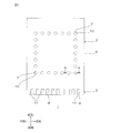
- FIG. 1 is a bottom view of an image sensor mounting substrate which is an embodiment of a flexible printed circuit board according to the present invention.
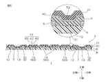
- FIG. 2 is a cross-sectional view taken along the line AA of the image sensor mounting substrate shown in FIG. 3A to 3D show manufacturing process diagrams of the image sensor mounting substrate shown in FIG. 2.
- FIG. 3A shows a metal support preparation process and a base insulating layer formation process
- FIG. 3B shows a conductor pattern formation process
- FIG. 3D shows the metal support removing step.
- FIG. 4 shows an imaging apparatus including the imaging element mounting substrate shown in FIG.
- FIG. 5 shows a cross-sectional view of a modified example of the image pickup device mounting substrate shown in FIG.
- FIG. 6A and 6B are front views of a warpage evaluation method in the example
- FIG. 6A is a step of preparing a substrate assembly sheet including a plurality of mounting substrates
- FIG. 6B is a diagram of apexes in the substrate assembly sheet. The process of measuring the height of a lower end part is shown.
- the vertical direction of the paper is the front-back direction (first direction)
- the upper side of the paper is the front side (one side in the first direction)
- the lower side of the paper surface is the rear side (the other side in the first direction).
- the left and right direction on the paper surface is the left and right direction (second direction orthogonal to the first direction), the left side on the paper surface is the left side (second side in the second direction), and the right side on the paper surface is the right side (the other side in the second direction). is there.
- the paper thickness direction is the vertical direction (an example of the thickness direction, a third direction orthogonal to the first direction and the second direction), and the back side of the paper is the upper side (an example of one side in the thickness direction, third One side in the direction) and the front side in the drawing are the lower side (an example of the other side in the thickness direction, the other side in the third direction).
- Imaging Element Mounting Board An imaging element mounting board 1 (hereinafter also simply referred to as a mounting board 1) that is an embodiment of the flexible printed circuit board of the present invention will be described.
- the mounting substrate 1 is a flexible printed circuit board (FPC) for mounting an image sensor 21 (see FIG. 4 to be described later), and does not include the image sensor 21 yet.
- the mounting substrate 1 has a substantially rectangular (rectangular) flat plate shape (sheet shape) in plan view extending in the front-rear direction and the left-right direction (plane direction).
- the mounting substrate 1 includes a housing arrangement portion 2 and an external component connection portion 3.
- the housing arrangement portion 2 is a portion where the housing 22 (see FIG. 4 described later) and the image sensor 21 are arranged. Specifically, when the housing 22 is disposed on the mounting substrate 1, it is a portion overlapping with the housing 22 when projected in the thickness direction.
- a plurality of image sensor connection terminals 10 as an example of terminals for electrical connection with the image sensor 21 are arranged at a substantially central portion of the housing arrangement portion 2.
- the external component connecting portion 3 is an area other than the housing arrangement portion 2 and is a portion for connecting to an external component.
- the external component connection portion 3 is arranged on the rear side of the housing arrangement portion 2 such that the front end edge of the external component connection portion 3 is continuous with the rear end edge of the housing arrangement portion 2.
- a plurality of external component connection terminals 11 as an example of terminals for electrical connection with external components are arranged at the rear end edge of the external component connection portion 3.
- the mounting substrate 1 has a base insulating layer 4 as an example of a first insulating layer, a conductor pattern 5, and a cover insulating layer 6 as an example of a second insulating layer on the upper side (thickness direction). It prepares in order toward an example of one side.
- the base insulating layer 4 has an outer shape of the mounting substrate 1 and is formed in a substantially rectangular shape in bottom view.
- the base insulating layer 4 forms a lower layer of the mounting substrate 1.
- the lower surface (an example of the other surface in the thickness direction) of the insulating base layer 4 is formed to be flat. Further, the entire lower surface of the base insulating layer 4 is exposed downward (an example of the other side in the thickness direction).
- the base insulating layer 4 is located in the lowermost layer of the mounting substrate 1, and the lower surface of the base insulating layer 4 is a metal support as described in Patent Document 1 (see reference numeral 19 in FIGS. 3A to 3C). Therefore, the mounting substrate 1 does not include the metal support 19 (metal support layer).
- the base insulating layer 4 is formed with a plurality of image sensor openings 7 and a plurality of external component openings 8 (see FIG. 1).
- the plurality of external component openings 8 are openings for exposing the external component connection terminals 11 from the lower surface.
- the external component openings 8 are aligned and arranged at the rear end edge of the external component connection portion 3 at intervals in the left-right direction.
- Each of the plurality of external component openings 8 penetrates the base insulating layer 4 in the vertical direction and has a substantially rectangular shape (rectangular shape) when viewed from the bottom.
- the external component opening 8 is formed so as to extend from the rear end edge of the external component connection portion 3 toward the front side in a bottom view.
- the base insulating layer 4 contains an insulating material.
- insulating material a material that satisfies the hygroscopic expansion coefficient (CHE) described below is selected.
- insulating materials include those having a desired hygroscopic expansion coefficient from synthetic resins such as polyimide, polyamideimide, acrylic, polyethernitrile, polyethersulfone, polyethylene terephthalate, polyethylene naphthalate, and polyvinyl chloride.
- synthetic resins such as polyimide, polyamideimide, acrylic, polyethernitrile, polyethersulfone, polyethylene terephthalate, polyethylene naphthalate, and polyvinyl chloride.
- a polyimide is mentioned from a viewpoint of insulation, heat resistance, and chemical resistance.
- Polyimide is, for example, a reaction product (cured product) obtained by reacting an acid dianhydride component and a diamine component.
- aromatic dianhydride examples include pyromellitic dianhydride such as 3,3 ′, 4,4′-benzophenonetetracarboxylic dianhydride, 2,2 ′, 3,3′-benzophenonetetra Benzophenone tetracarboxylic dianhydrides such as carboxylic dianhydrides such as 3,3 ′, 4,4′-biphenyltetracarboxylic dianhydride (BPDA), 2,2 ′, 3,3′-biphenyltetra Biphenyltetracarboxylic dianhydrides such as carboxylic dianhydrides, 2,3,3 ′, 4′-biphenyltetracarboxylic dianhydrides, 2,2 ′, 6,6′-biphenyltetracarboxylic dianhydrides
- BPDA 4,4′-biphenyltetracarboxylic dianhydride
- aliphatic acid dianhydride examples include ethylene tetracarboxylic dianhydride, butane tetracarboxylic dianhydride, cyclobutane tetracarboxylic dianhydride, cyclopentane tetracarboxylic dianhydride, and the like.
- the acid dianhydride component is preferably an aromatic acid dianhydride from the viewpoint of obtaining excellent heat resistance, and more preferably, from the viewpoint of reducing the hygroscopic expansion coefficient, biphenyltetracarboxylic dianhydride is More preferably, BPDA is mentioned.
- diamine component examples include aromatic diamines and aliphatic diamines.
- aromatic diamine examples include phenylene diamines such as p-phenylene diamine (PPD), m-phenylene diamine, and o-phenylene diamine, such as 3,3′-diaminodiphenyl ether, 3,4′-diaminodiphenyl ether, 4, Diaminodiphenyl ethers such as 4'-diaminodiphenyl ether, for example 3,3'-diaminodiphenyl sulfide, 3,4'-diaminodiphenyl sulfide, diaminodiphenyl sulfide such as 4,4'-diaminodiphenyl sulfide, for example 3,3 ' -Diaminodiphenyl sulfones such as diaminodiphenyl sulfone, 3,4'-diaminodiphenyl sulfone, 4,4'-diaminodiphenyl sulf
- a is 0 or a natural number of 1 or more, and the amino group is bonded to the meta position or the para position with respect to the bond between the benzene rings.
- aromatic diamine represented by the formula (A) include benzidine.
- a represents a natural number of 0 or 1 or more, and R represents a substituent. However, the amino group is bonded to the meta position or the para position with respect to the bond between benzene rings.
- the substituent represented by R is a monovalent organic group, but they may be bonded to each other. Examples of the substituent represented by R include an alkyl group having 3 or less carbon atoms such as methyl, and a haloalkyl group having 3 or less carbon atoms such as trifluoromethyl, perfluoroethyl, and perfluoropropyl (preferably a fluoroalkyl group). Examples thereof include halogen atoms such as chloro and fluoro.
- the substituent represented by R is preferably a haloalkyl group, more preferably a fluoroalkyl group.
- Specific examples of the aromatic diamine having a substituent and represented by the formula (B) include, for example, 2,2′-dimethyl-4,4′-diaminobiphenyl, 2,2′-ditrifluoromethyl-4, 4′-diaminobiphenyl (also known as 2,2′-bis (trifluoromethyl, TFMB) -4,4′-diaminobiphenyl), 3,3′-dichloro-4,4′-diaminobiphenyl, 3,3 ′ -Dimethoxy-4,4'-diaminobiphenyl, 3,3'-dimethyl-4,4'-diaminobiphenyl.
- Examples of the aliphatic diamine include bis (aminomethyl) ether, bis (2-aminoethyl) ether, bis (3-aminopropyl) ether, bis (2-aminomethoxy) ethyl] ether, bis [2- (2- Aminoethoxy) ethyl] ether, bis [2- (3-aminoprotoxy) ethyl] ether, 1,2-bis (aminomethoxy) ethane, 1,2-bis (2-aminoethoxy) ethane, 1,2- Bis [2- (aminomethoxy) ethoxy] ethane, 1,2-bis [2- (2-aminoethoxy] ethane, ethylene glycol bis (3-aminopropyl) ether, diethylene glycol bis (3-aminopropyl) ether , Triethylene glycol bis (3-aminopropyl) ether, ethylenediamine, 1,3-di Minopropane, 1,
- the diamine component is preferably an aromatic diamine from the viewpoint of obtaining excellent heat resistance, and more preferably a substituent having a fluorine atom (specifically, fluorocarbon from the viewpoint of further reducing the hygroscopic expansion coefficient).
- An aromatic diamine having an alkyl group or a halogen atom more preferably an aromatic diamine having a fluoroalkyl group as a substituent, and particularly preferably TFMB.
- the diamine component can be used alone or in combination.
- a plurality of different types of aromatic diamines are preferable, and a combination of phenylenediamine and a diamine having a fluoroalkyl group is more preferable.
- Such a combination is described in detail in, for example, Japanese Patent Application Laid-Open No. 2013-100441.
- the molar ratio of the aromatic diamine having a fluoroalkyl group is, for example, 15% or more, preferably 20% or more, and, for example, 80%, relative to the total number of moles of phenylenediamine and diamine having a fluoroalkyl group. Hereinafter, it is preferably 50% or less.
- the acid dianhydride component and the diamine component are appropriately selected from the above examples so that the insulating material has a desired hygroscopic expansion coefficient.
- the acid dianhydride component contains 3,3 ′, 4,4′-biphenyltetracarboxylic dianhydride (BPDA), and the diamine component is 2,2′-ditrifluoromethyl-4,4′-diamino.
- BPDA 4,4′-biphenyltetracarboxylic dianhydride
- TFMB 2,2′-ditrifluoromethyl-4,4′-diamino.
- the polyimide includes a structural unit represented by the following formula (1).
- the polyimide contains the structural unit represented by the formula (1), it is possible to suppress warpage of the mounting substrate 1 while ensuring a low hygroscopic expansion coefficient while being excellent in heat resistance.
- x is 15 or more and 80 or less.
- x is preferably 20 or more, and preferably 50 or less.
- x is not less than the above lower limit, a low hygroscopic expansion coefficient can be ensured. If x is below the above-mentioned upper limit, when preparing a varnish, it can be easily dissolved in a solvent.
- the hygroscopic expansion coefficient of the insulating material is 15 ⁇ 10 ⁇ 6 /% RH or less, preferably 13 ⁇ 10 ⁇ 6 /% RH or less, for example, 0 ⁇ 10 ⁇ 6 /% RH or more, preferably It is 1 ⁇ 10 ⁇ 6 /% RH or more.
- the warp of the base insulating layer 4 and consequently the warp of the mounting substrate 1 cannot be suppressed.
- the hygroscopic expansion coefficient of the insulating material is equal to or less than the above upper limit, the warp of the base insulating layer 4 can be suppressed, and consequently the warp of the mounting substrate 1 can be suppressed.
- the hygroscopic expansion coefficient of the insulating material for forming the base insulating layer 4 is, for example, the same as the hygroscopic expansion coefficient of the base insulating layer 4 after curing in the mounting substrate 1.
- the hygroscopic expansion coefficient of the insulating material is measured according to the description in the examples of JP 2013-100441 A.
- the thickness T1 of the insulating base layer 4 is, for example, 12 ⁇ m or less, preferably 8 ⁇ m or less, and for example, 1 ⁇ m or more, preferably 3 ⁇ m or more.
- the thickness T1 of the insulating base layer 4 is adjusted so that the total of the thickness T1 of the insulating base layer 4 and the thickness T2 of the insulating cover layer 6 to be described later falls within a desired range.
- the conductor pattern 5 is provided on the upper side of the insulating base layer 4 so as to be in contact with the upper surface of the insulating base layer 4.
- the conductor pattern 5 includes a plurality of image sensor connection terminals 10, a plurality of external component connection terminals 11 (see FIG. 2), and a plurality of wirings 9.
- the plurality of image sensor connection terminals 10 are arranged at intervals in the center of the housing arrangement portion 2 so as to form a rectangular frame. That is, as shown in FIG. 2, the plurality of image sensor connection terminals 10 are provided so as to correspond to the plurality of terminals 25 (see FIG. 4) of the image sensor 21 to be mounted. In addition, the plurality of image sensor connection terminals 10 are provided corresponding to the plurality of image sensor openings 7.
- the image sensor connection terminal 10 has a substantially circular shape in bottom view.
- the image sensor connection terminal 10 is formed so as to protrude downward in a cross-sectional view (a side cross-sectional view and a normal cross-sectional view).
- the image pickup device connection terminal 10 includes an outer peripheral portion 12 arranged on the outer periphery of the image pickup device opening portion 7, and an inner portion 13 arranged in the image pickup device opening portion 7 so as to be recessed inward from the outer peripheral portion 12. Is integrally provided.
- the lower surface (exposed surface) of the inner portion 13 is exposed from the image sensor opening 7 and is formed to be flat. Further, the lower surface of the inner portion 13 is formed so as to be flush with the lower surface of the base insulating layer 4.
- the plurality of external component connection terminals 11 are arranged at the rear end edge of the external component connection portion 3 so as to be spaced apart from each other in the left-right direction. That is, it is provided so as to correspond to a plurality of terminals (not shown) of the external component.
- the plurality of external component connection terminals 11 are provided corresponding to the plurality of external component openings 8.
- the external component connection terminal 11 has a substantially rectangular shape (rectangular shape) in plan view.
- the external component connection terminal 11 is disposed in the external component opening 8 and its lower surface is exposed from the external component opening 8.
- the plurality of wirings 9 include a plurality of connection wirings 14 and a plurality of ground wirings 15 as shown in FIG.
- connection wiring 14 are provided so as to correspond to the plurality of image sensor connection terminals 10 and the plurality of external component connection terminals 11.
- the connection wiring 14 is integrally formed with the image sensor connection terminal 10 and the external component connection terminal 11 so as to connect them. That is, one end of the connection wiring 14 is continuous with the image sensor connection terminal 10, and the other end of the connection wiring 14 is continuous with the external component connection terminal 11 to electrically connect them.
- the plurality of ground wirings 15 are provided so as to correspond to the plurality of connection wirings 14. Specifically, the plurality of ground wirings 15 are provided outside the plurality of connection wirings 14 along these. A ground terminal (not shown) is integrally connected to one end of the ground wiring 15.
- Examples of the material of the conductive pattern 5 include metal materials such as copper, silver, gold, nickel, alloys containing them, and solder. Preferably, copper is used.
- the thickness of the conductor pattern 5 is, for example, 1 ⁇ m or more, preferably 3 ⁇ m or more, and for example, 15 ⁇ m or less, preferably 10 ⁇ m or less.
- the width of the wiring 9 is, for example, 5 ⁇ m or more, preferably 10 ⁇ m or more, and for example, 100 ⁇ m or less, preferably 50 ⁇ m or less.
- the insulating cover layer 6 is provided on the upper side of the insulating base layer 4 and the conductive pattern 5 so as to cover the conductive pattern 5. That is, the insulating cover layer 6 is disposed so as to contact the upper surface and side surfaces of the conductor pattern 5 and the upper surface of the insulating base layer 4 exposed from the conductive pattern 5.
- the insulating cover layer 6 forms the upper layer of the mounting substrate 1.
- the outer shape of the insulating cover layer 6 is formed to be the same as that of the insulating base layer 4 except for the portion where the external component connection terminals 11 are formed.
- the insulating cover layer 6 contains an insulating material similar to the insulating material described above for the insulating base layer 4.
- the hygroscopic expansion coefficient of the insulating material for forming the insulating cover layer 6 is, for example, the same as the hygroscopic expansion coefficient of the insulating material for forming the insulating base layer 4.
- the hygroscopic expansion coefficient of the insulating material is measured according to the description in the examples of JP 2013-100441 A.
- the hygroscopic expansion coefficient of the insulating material for forming the insulating cover layer 6 is 15 ⁇ 10 ⁇ 6 /% RH or less, preferably 13 ⁇ 10 ⁇ 6 /% RH or less. 0 ⁇ 10 ⁇ 6 /% RH or more, preferably 1 ⁇ 10 ⁇ 6 /% RH or more.
- the hygroscopic expansion coefficient of the insulating material exceeds the upper limit described above, the warp of the cover insulating layer 6 and consequently the warp of the mounting substrate 1 cannot be suppressed.
- the hygroscopic expansion coefficient of the insulating material is equal to or less than the above upper limit, the warp of the cover insulating layer 6 can be suppressed, and consequently the warp of the mounting substrate 1 can be suppressed.
- the thickness T2 of the insulating cover layer 6 is, for example, 6 ⁇ m or less, preferably 4 ⁇ m or less, and for example, 1 ⁇ m or more, preferably 2 ⁇ m or more.
- the thickness T2 of the insulating cover layer 6 is adjusted so that the total of the thickness T1 of the insulating base layer 4 and the thickness T2 of the insulating cover layer 6 described below is within a desired range.
- the total of the thickness T1 of the base insulating layer 4 and the thickness T2 of the cover insulating layer 6 is 16 ⁇ m or less, preferably 13 ⁇ m or less, more preferably 10 ⁇ m or less. It is 1 ⁇ m or more, preferably 5 ⁇ m or more.
- the total thickness of the base insulating layer 4 and the cover insulating layer 6 is the thickness of the base insulating layer 4 and the cover insulating layer 6 that are in contact with each other in the thickness direction in the region where the conductor pattern 5 is not formed.
- the problem that the mounting substrate 1 tends to warp does not occur.
- the total thickness of the insulating base layer 4 and the insulating cover layer 6 is equal to or less than the above-described upper limit, a problem (the problem of the present invention) that the mounting substrate 1 is easily warped occurs.
- the base insulating layer 4 contains an insulating material having a hygroscopic expansion coefficient of 15 ⁇ 10 ⁇ 6 /% RH or less. Warpage can be suppressed.
- the ratio (T1 / T2) of the thickness T1 of the base insulating layer 4 to the thickness T2 of the cover insulating layer 6 is, for example, 5 or less, preferably 1.8 or less, and for example, 1 or more, preferably 1 .3 or more.
- the thickness of the mounting substrate 1 (total thickness of the base insulating layer 4, the conductor pattern 5, and the cover insulating layer 6) is, for example, 50 ⁇ m or less, preferably 30 ⁇ m or less, more preferably 20 ⁇ m or less, and for example, 1 ⁇ m. As mentioned above, Preferably, it is 5 micrometers or more.
- the mounting board 1 includes, for example, a metal support preparing process, a base insulating layer forming process, a conductor pattern forming process, a cover insulating layer forming process, and a metal It is obtained by carrying out the support removing step in order.
- a metal support 19 is prepared in the metal support preparation step.
- the metal support 19 has a flat plate shape (sheet shape) having a substantially rectangular shape (rectangular shape) in plan view extending in the surface direction.
- the metal support 19 is made of a metal material such as stainless steel, 42 alloy, or aluminum. Preferably, it is formed from stainless steel.
- the thickness of the metal support 19 is, for example, 5 ⁇ m or more, preferably 10 ⁇ m or more, for example, 50 ⁇ m or less, preferably 30 ⁇ m or less.
- the upper surface of the metal support 19 is formed to be flat (smooth).
- the base insulating layer 4 is formed on the upper surface of the metal support 19. That is, the base insulating layer 4 having the image sensor opening 7 and the external component opening 8 is formed on the upper surface of the metal support 19.
- a photosensitive insulating material varnish is prepared.
- the varnish can contain a solvent capable of dissolving the above acid dianhydride component and diamine in an appropriate ratio, and further, a photosensitizer, a sensitizer, a polymerization terminator, Additives such as chain transfer agents, leveling agents, plasticizers, surfactants and antifoaming agents can be contained in appropriate proportions.
- varnish is applied to the entire upper surface of the metal support 19 and then the solvent is dried. Thereby, a base film is formed. Thereafter, the base film is exposed through a photomask having a pattern corresponding to the image sensor opening 7 and the external component opening 8. Thereafter, the base film is developed, and then heat-cured as necessary.
- the conductor pattern 5 is formed in the above-described pattern by using the upper surface of the base insulating layer 4 and the upper surface of the mounting substrate 1 exposed from the imaging element opening 7 and the external component opening 8. And form.
- the conductor pattern 5 is formed by, for example, an additive method.
- the insulating cover layer 6 is disposed on the upper surfaces of the conductor pattern 5 and the insulating base layer 4.
- the cover insulating layer forming step is performed in the same manner as the base insulating layer forming step.
- the mounting substrate 1 including the base insulating layer 4, the conductor pattern 5, and the cover insulating layer 6 is obtained while being supported by the metal support 19.
- the mounting substrate 1 includes a metal support 19 and has not been removed yet. Therefore, the mounting substrate 1 is not included in the flexible printed circuit board of the present invention.
- the metal support 19 is removed.
- the metal support 19 is exposed from the lower surface of the base insulating layer 4, the lower surface of the image sensor connection terminal 10 exposed from the image sensor opening 7, and the external component opening 8.
- a method of peeling from the lower surface of the external component connection terminal 11, for example, a method of performing etching such as dry etching or wet etching on the metal support 19 is exemplified. Etching is preferable, and wet etching is more preferable. In the wet etching, there is a chemical etching method in which a ferric chloride aqueous solution or the like is used as an etching solution and sprayed or immersed.
- the mounting substrate 1 does not include the metal support 19 and preferably includes only the insulating base layer 4, the conductor pattern 5, and the insulating cover layer 6.
- the mounting substrate 1 can be used for the application described below and can exhibit operational effects by removing the metal support 19.
- Such a mounting substrate 1 is used, for example, as an image sensor mounting substrate for mounting an image sensor. That is, the mounting substrate 1 is provided in an imaging device such as a camera module.
- the mounting substrate 1 is not an imaging device described below, but is a component of the imaging device, that is, a component for manufacturing the imaging device, does not include an imaging element, and specifically, the component alone is distributed. However, it is an industrially available device.
- Imaging Device 20 including the mounting substrate 1 will be described as an example of the imaging device of the present invention.
- the imaging device 20 includes a mounting substrate 1, an imaging element 21, a housing 22, an optical lens 23, and a filter 24.
- the mounting substrate 1 is provided in the imaging device 20 by turning the mounting substrate 1 shown in FIG. 2 upside down. That is, the mounting substrate 1 is arranged so that the insulating base layer 4 is on the upper side (the other side in the thickness direction) and the insulating cover layer 6 is on the lower side (the one side in the thickness direction).
- the imaging element 21 is a semiconductor element that converts light into an electrical signal, and examples thereof include solid-state imaging elements such as a CMOS sensor and a CCD sensor.
- the imaging element 21 is formed in a substantially rectangular flat plate shape in plan view, and includes a silicon such as a Si substrate, a photodiode (photoelectric conversion element), and a color filter arranged on the silicon substrate (not shown).
- a plurality of terminals 25 corresponding to the image sensor connection terminals 10 of the mounting substrate 1 are provided on the lower surface of the image sensor 21.
- the thickness of the imaging element 21 is, for example, 10 ⁇ m or more, preferably 50 ⁇ m or more, and for example, 1000 ⁇ m or less, preferably 500 ⁇ m or less.
- the image sensor 21 is mounted on the mounting substrate 1. Specifically, the terminals 25 of the image sensor 21 are flip-chip mounted via the corresponding image sensor connection terminals 10 of the mounting substrate 1 and solder bumps 26. As a result, the image sensor 21 is arranged at the center of the housing arrangement part 2 of the mounting substrate 1 and is electrically connected to the image sensor connection terminal 10 and the external component connection terminal 11 of the mounting substrate 1.
- the imaging element 21 constitutes an imaging unit 27 by being mounted on the mounting substrate 1. That is, the imaging unit 27 includes the mounting substrate 1 and the imaging element 21 mounted thereon.
- the housing 22 is arranged in the housing arrangement portion 2 of the image pickup device 21 so as to surround the image pickup device 21 with an interval.
- the housing 22 has a substantially rectangular tube shape in plan view.
- a fixing portion for fixing the optical lens 23 is provided at the upper end of the housing 22.
- the optical lens 23 is disposed on the upper side of the mounting substrate 1 with a distance from the mounting substrate 1 and the imaging element 21.
- the optical lens 23 is formed in a substantially circular shape in plan view, and is fixed by a fixing portion so that light from the outside reaches the image sensor 21.
- the filter 24 is disposed at the center of the imaging element 21 and the optical lens 23 in the vertical direction with a space therebetween and is fixed to the housing 22.
- the total thickness (T1 + T2) of the base insulating layer 4 and the cover insulating layer 6 is as thin as 16 ⁇ m or less, it can be reduced in thickness.
- the entire lower surface of the base insulating layer 4 is exposed downward, and the base insulating layer 4 is 15 ⁇ 10 ⁇ 6 /% RH or less. Since an insulating material having a low hygroscopic expansion coefficient is contained, warping can be suppressed.
- the mounting substrate 1 includes the metal support 19
- the rigidity of the metal support 19 is high.
- the base insulating layer 4 and the cover insulating layer 6 are excessively restrained, and on the contrary, a warp defect becomes apparent.
- the base insulating layer 4 and the cover insulating layer 6 can be released from the restraint of the metal support 19. This also exposes the entire bottom surface of the base insulating layer 4, but the base insulating layer 4 is made of an insulating material having a low hygroscopic expansion coefficient. Therefore, warpage can be suppressed.
- the insulating material is a polyimide containing the structural unit represented by the formula (1), it is possible to suppress warpage of the mounting substrate 1 while ensuring a low hygroscopic expansion coefficient while being excellent in heat resistance.
- the conductor pattern 5 includes the image sensor connection terminal 10 and the external component connection terminal 11 exposed downward from the base insulating layer 4, so that they are reliably electrically connected to the image sensor 21 and the external component. Can be connected to.
- the mounting substrate 1 is the image sensor mounting substrate 1 on which the image sensor 21 is mounted, it is possible to provide an imaging device with a reduced thickness, and the warping of the mounting substrate 1 is suppressed. Therefore, in the imaging device 20, the connection reliability between the mounting substrate 1 and the imaging element 21 can be improved.
- the hygroscopic expansion coefficient of the insulating material for forming the insulating cover layer 6 is set to be the same as the hygroscopic expansion coefficient of the insulating material for forming the base insulating layer 4, but the present invention is not limited to this.
- the hygroscopic expansion coefficient of the insulating material for forming the insulating cover layer 6 may be outside the range of the hygroscopic expansion coefficient of the insulating material for forming the insulating base layer 4. In short, it is sufficient that at least the insulating material for forming the insulating base layer 4 has a desired hygroscopic expansion coefficient.
- the flexible wiring circuit board of the present invention is described as the imaging element mounting board 1 (mounting board 1) for mounting the imaging element 21, but the use of the flexible wiring circuit board is limited to this. Not. For example, it is suitably used for various applications that require reduction in thickness and warpage, specifically, mounting substrates such as pressure sensors, acceleration sensors, gyro sensors, ultrasonic sensors, and fingerprint authentication sensors.
- the wiring 9 includes the ground wiring 15, but for example, although not illustrated, the ground wiring 15 may not be provided. That is, the wiring 9 can also be configured only from the connection wiring 14.
- the imaging element 21 is flip-chip mounted on the mounting substrate 1.
- the imaging element 21 is mounted on the mounting substrate 1. It can also be mounted by wire bonding.
- the mounting substrate 1 includes only the base insulating layer 4, the conductor pattern 5, and the cover insulating layer 6.
- the substrate 1 further includes a shield layer 40 and a second cover insulating layer 31 as an example of a third insulating layer.
- the mounting substrate 1 includes a base insulating layer 4, a conductor pattern 5, a cover insulating layer (first cover insulating layer) 6, a shield layer 40, and a second cover insulating layer 31 in order toward the upper side. .
- the shield layer 40 is disposed on the upper side of the insulating cover layer 6 so as to be in contact with the upper surface of the insulating cover layer 6.
- the shield layer 40 is a layer that shields electromagnetic waves from the outside, and is formed in a sheet shape extending in the plane direction (front-rear direction and left-right direction).
- the shield layer 40 is electrically connected to the ground wiring 15. That is, the shield layer 40 is continuous with the ground wiring 15. Specifically, the shield layer 40 includes a contact portion 41 having a convex shape on the lower side and in contact with the upper surface of the ground wiring 15 at a portion facing the ground wiring 15.
- the contact portion 41 includes a flat portion 42 that directly contacts the ground wiring 15 and an inclined portion 43 that is integrally disposed so as to be continuous around the flat portion 42.
- the flat part 42 is formed in a flat plate shape extending in the surface direction.
- the inclined portion 43 extends in an inclination direction that intersects (inclines) the vertical direction and the surface direction.
- the shield layer 40 is grounded via the ground wiring 15.
- the shield layer 40 is made of a conductor, and for example, a metal material such as copper, chromium, nickel, gold, silver, platinum, palladium, titanium, tantalum, solder, or an alloy thereof is used. Preferably, copper is used.
- the thickness of the shield layer 40 is, for example, 0.05 ⁇ m or more, preferably 0.1 ⁇ m or more, and for example, 3 ⁇ m or less, preferably 1 ⁇ m or less.
- the second cover insulating layer 31 is provided on the upper side of the shield layer 40 so as to cover the shield layer 40.
- the outer shape of the second insulating cover layer 31 is formed to be the same as that of the insulating cover layer 6.
- the second cover insulating layer 31 contains an insulating material similar to the insulating material described above for the base insulating layer 4.
- the hygroscopic expansion coefficient of the insulating material for forming the second cover insulating layer 31 is the same as the hygroscopic expansion coefficient of the insulating material for forming the base insulating layer 4.
- the hygroscopic expansion coefficient of the insulating material for forming the second cover insulating layer 31 is 15 ⁇ 10 ⁇ 6 /% RH or less, preferably 13 ⁇ 10 ⁇ 6 /% RH or less.
- it is 0 ⁇ 10 ⁇ 6 /% RH or more, preferably 1 ⁇ 10 ⁇ 6 /% RH or more.
- the warp of the second cover insulating layer 31 and consequently the warp of the mounting substrate 1 cannot be suppressed.
- the hygroscopic expansion coefficient of the insulating material is equal to or less than the upper limit described above, the warp of the second cover insulating layer 31 can be suppressed, and consequently the warp of the mounting substrate 1 can be suppressed.
- the thickness T3 of the second cover insulating layer 31 is, for example, 3 ⁇ m or less, preferably 2 ⁇ m or less, for example, 0.1 ⁇ m or more, preferably 1 ⁇ m or more.
- the total of the thickness T1 of the insulating base layer 4, the thickness T2 of the insulating cover layer 6, and the thickness T3 of the second insulating cover layer 31 (total thickness of the insulating layer, T1 + T2 + T3) is 16 ⁇ m or less, preferably 13 ⁇ m or less, more preferably For example, it is 1 ⁇ m or more, preferably 5 ⁇ m or more. If the total thickness of the base insulating layer 4, the cover insulating layer 6, and the second cover insulating layer 31 is equal to or less than the above upper limit, warpage of the second cover insulating layer 31 can be suppressed.
- the second cover insulating layer 31 contains an insulating material having a hygroscopic expansion coefficient of 15 ⁇ 10 ⁇ 6 /% RH or less.
- the mounting substrate 1 shown in FIG. 5 is obtained in a state where the mounting substrate 1 of the embodiment is supported by the metal support 19, and then the shield layer 40 and the second cover insulating layer 31 are provided in this order in the first cover insulation. It can be produced by forming on the top surface of the layer 6 and subsequently removing the metal support 19.
- a part of the conductor pattern 5 can be exposed from the insulating cover layer 6.
- a plurality of mounting boards 1 can be configured as a board assembly sheet 50.
- the board assembly sheet 50 includes a plurality of mounting boards 1 that are aligned in the plane direction.
- this invention is not limited to a manufacture example, a comparative manufacture example, an Example, and a comparative example.
- specific numerical values such as a blending ratio (content ratio), physical property values, and parameters used in the following description are described in the above-mentioned “Mode for Carrying Out the Invention”, and a blending ratio corresponding to them ( It may be replaced with the upper limit (numerical values defined as “less than” or “less than”) or lower limit (numerical values defined as “greater than” or “exceeded”) such as content ratio), physical property values, parameters, etc. it can.
- nifedipine photosensitive agent
- Comparative production example 1 instead of 4.0 g (20 mmol) of 2,2′-bis (trifluoromethyl) -4,4′-diaminobiphenyl (TFMB) and 8.65 g (80 mmol) of p-phenylenediamine (PPD), 4,4 Except for changing to 3.0 g (15 mmol) of '-diaminodiphenyl ether (ODA, 4,4'-oxybis (benzeneamine), aromatic diamine) and 9.19 g (85 mmol) of paraphenylenediamine (PPD, aromatic diamine) Were processed in the same manner as in Production Example 1 to prepare a polyimide precursor solution B and then a photosensitive polyimide precursor solution B.
- ODA '-diaminodiphenyl ether
- PPD paraphenylenediamine
- Example 1 As shown in FIG. 3A, a metal support 19 made of stainless steel having a thickness of 18 ⁇ m was prepared.
- the polyimide precursor solution A of Production Example 1 was applied to the upper surface of the metal support 19, and then dried at 80 ° C. for 10 minutes to form a base film (polyimide precursor film). Subsequently, the base film was exposed through a photomask and subsequently developed. Thereafter, the base film was heated (cured) at 360 ° C. for 1 hour in a nitrogen atmosphere to form a base insulating layer 4 made of polyimide and having an imaging element opening 7 and an external part opening 8 having a thickness of 10 ⁇ m. .
- the conductor pattern 5 made of copper and having a thickness of 8 ⁇ m is formed on the upper surface of the base insulating layer 4 and the upper surface of the metal support 19 exposed from the imaging element opening 7 and the external component opening 8. It was formed by the additive method.
- the polyimide precursor solution of Production Example 1 was applied to the upper surfaces of the base insulating layer 4 and the conductor pattern 5, and then dried at 80 ° C. for 10 minutes to obtain a cover film (polyimide precursor film). ) was formed. Subsequently, the cover film was exposed through a photomask and subsequently developed. Then, the cover insulating layer 6 made of polyimide and having a thickness of 5 ⁇ m was obtained by heating the cover film at 360 ° C. for 1 hour in a nitrogen atmosphere.
- the metal support 19 was removed by a chemical etching method in which an etching solution comprising a ferric chloride aqueous solution was sprayed from below. As a result, the entire lower surface of the base insulating layer 4 was exposed.
- the mounting substrate 1 including the base insulating layer 4, the conductor pattern 5, and the cover insulating layer 6 in which the entire lower surface is exposed was obtained.
- Both the base insulating layer 4 and the cover insulating layer 6 have a structural unit represented by the formula (2).
- Formula (2) :
- Examples 2 and 3 and Comparative Example 1 A mounting substrate 1 was obtained in the same manner as in Example 1 except that the formulation, thickness, heating temperature, and the like of each layer were changed based on the description in Table 1.
- Example 4 The mounting substrate 1 including the base insulating layer 4, the conductor pattern 5, the cover insulating layer 6, the shield layer 40, and the second cover insulating layer 31 in order was obtained.
- the base insulating layer 4, the conductor pattern 5, and the cover insulating layer 6 were formed in the same manner as in Example 3.
- a shield layer 40 made of copper having a thickness of 0.1 ⁇ m is formed by sputtering, In the same manner as the base insulating layer 4, the second cover insulating layer 31 was formed from polyimide having a thickness of 2 ⁇ m.
- Comparative Example 2 The processing was performed in the same manner as in Example 2 except that the mounting substrate 1 including the metal support 19 was manufactured without removing the metal support 19.
- the entire lower surface of the base insulating layer 4 is covered with a metal support 19.
- Comparative Example 3 The same treatment as in Comparative Example 1 was performed except that the mounting substrate 1 including the metal support 19 was manufactured without removing the metal support 19.
- the entire lower surface of the base insulating layer 4 is covered with a metal support 19.
- Table 1 shows the layer configuration and thickness of each example and each comparative example.
- the sample was sufficiently dried, and then the sample was placed in a chamber of a humidity type thermomechanical analyzer (HC-TMA4000SA, manufactured by Bruker AXS) at 30 ° C. in an environment of 5% RH for 3 hours.
- HC-TMA4000SA a humidity type thermomechanical analyzer
- a load 196 mN
- the relative humidity was changed to 75% RH and held for 3 hours to stabilize.
- the hygroscopic expansion coefficient was obtained from the sample elongation and the amount of change in relative humidity (70% RH) by the arithmetic processing of the humidity type thermomechanical analyzer.
- a substrate assembly sheet 50 including nine mounting substrates 1 was prepared.
- the external size of each mounting substrate 1 was 15 mm ⁇ 15 mm, and the external size of the substrate assembly sheet 50 was 45 mm ⁇ 45 mm.
- the substrate assembly sheet 50 was placed on the surface of the flat plate 45 in an environment of a temperature of 25 ° C. and a humidity of 60% RH.
- the heights (h1, h2, h3, h4) of the respective lower ends at the four vertices of the substrate assembly sheet 50 and the surface of the flat plate 45 are measured.
- the average value ([h1 + h2 + h3 + h4] / 4) was calculated as the warp.
- the flexible printed circuit board is provided in the imaging device.
- Mounting substrate (Imaging device mounting substrate) 4 Base insulating layer 5 Conductor pattern 6 Cover insulating layer 10 Image sensor connection terminal 11 External component connection terminal 20 Imaging device 21 Image sensor 31 Second cover insulating layer 40 Shield layer 50 Substrate assembly sheet T1 Base insulating layer thickness T2 Cover insulation Layer thickness T3 Thickness of the second cover insulating layer
Landscapes
- Engineering & Computer Science (AREA)
- Microelectronics & Electronic Packaging (AREA)
- Chemical & Material Sciences (AREA)
- Medicinal Chemistry (AREA)
- Health & Medical Sciences (AREA)
- Chemical Kinetics & Catalysis (AREA)
- Manufacturing & Machinery (AREA)
- Polymers & Plastics (AREA)
- Organic Chemistry (AREA)
- Physics & Mathematics (AREA)
- Electromagnetism (AREA)
- Structure Of Printed Boards (AREA)
- Non-Metallic Protective Coatings For Printed Circuits (AREA)
- Macromolecular Compounds Obtained By Forming Nitrogen-Containing Linkages In General (AREA)
Abstract
実装基板は、ベース絶縁層と、導体パターンと、カバー絶縁層とを厚み方向一方側に向かって順に備える。ベース絶縁層の下面の全ては、下方に向かって露出する。ベース絶縁層およびカバー絶縁層の総厚みが、16μm以下である。ベース絶縁層は、15×10-6/%RH以下の吸湿膨張係数を有する絶縁材料を含有する。
Description
本発明は、フレキシブル配線回路基板、その製造方法および撮像装置に関する。
従来、絶縁層、配線層および被覆層が、この順に積層された配線回路基板が知られている。また、このような配線回路基板としては、絶縁層の裏面に金属支持体が設けられているものが知られている(例えば、特許文献1参照。)。
しかるに、配線回路基板の厚み、例えば、絶縁層および被覆層の総厚みが薄くなると、反りが発生し易くなるという不具合がある。
一方、上記した配線回路基板は、金属支持体を絶縁層の裏面に備えるので、金属支持体によって上記した反りを抑制できると考えられる。しかし、絶縁層および被覆層の総厚みが薄い場合には、逆に、上記した反りが顕在化するという不具合を生じる。
本発明の目的は、薄型化を図りながら、反りを抑制することのできるフレキシブル配線回路基板、その製造方法および撮像装置を提供することにある。
本発明(1)は、第1絶縁層と、導体パターンと、第2絶縁層とを厚み方向一方側に向かって順に備え、前記第1絶縁層の厚み方向他方面の全ては、厚み方向他方側に向かって露出し、前記第1絶縁層および前記第2絶縁層の総厚みが、16μm以下であり、少なくとも前記第1絶縁層は、15×10-6/%RH以下の吸湿膨張係数を有する絶縁材料を含有するフレキシブル配線回路基板を含む。
本発明(2)は、前記絶縁材料は、下記式(1)で示される構造単位を含むポリイミドである(1)に記載のフレキシブル配線回路基板を含む。
式(1):
式(1):

本発明(3)は、前記導体パターンは、前記第1絶縁層から厚み方向他方側に露出する端子を有する(1)または(2)に記載のフレキシブル配線回路基板を含む。
本発明(4)は、前記導体パターンの一部は、前記第2絶縁層から厚み方向一方側に露出する(1)~(3)のいずれか一項に記載のフレキシブル配線回路基板を含む。
本発明(5)は、シールド層と、第3絶縁層とをさらに備え、前記第1絶縁層と、前記導体パターンと、前記第2絶縁層と、前記シールド層と、前記第3絶縁層とを、厚み方向一方側に向かって順に備え、前記第1絶縁層、前記第2絶縁層および前記第3絶縁層の総厚みが、16μm以下である(1)~(4)のいずれか一項に記載のフレキシブル配線回路基板を含む。
本発明(6)は、前記第3絶縁層は、15×10-6/%RH以下の吸湿膨張係数を有する絶縁材料を含有する(5)に記載のフレキシブル配線回路基板を含む。
本発明(7)は、撮像素子を実装するための撮像素子実装基板である(1)~(6)のいずれか一項に記載のフレキシブル配線回路基板を含む。
本発明(8)は、(7)に記載される撮像素子実装基板と、前記撮像素子実装基板に実装される撮像素子とを備える、撮像装置を含む。
本発明(9)は、(1)~(7)のいずれか一項に記載のフレキシブル配線回路基板の製造方法であって、金属支持基板を用意する工程、前記金属支持基板の厚み方向一方側に、第1絶縁層と、導体パターンと、第2絶縁層とを順に形成する工程、および、前記金属支持基板を除去する工程を備えるフレキシブル配線回路基板の製造方法を含む。
本発明のフレキシブル配線回路基板では、第1絶縁層および第2絶縁層の総厚みが、16μm以下と薄いので、薄型化を図ることができる。
また、本発明のフレキシブル配線回路基板では、第1絶縁層の厚み方向他方面の全ては、厚み方向他方側に向かって露出し、かつ、少なくとも第1絶縁層は、15×10-6/%RH以下の低い吸湿膨張係数を有する絶縁材料を含有するので、反りを抑制することができる。
本発明の撮像装置は、上記したフレキシブル配線回路基板を撮像素子実装基板として備えるので、薄型化を図ることができ、接続信頼性を向上させることができる。
本発明のフレキシブル配線回路基板の製造方法によれば、薄型化が図られ、反りが抑制されたフレキシブル配線回路基板を得ることができる。
図1において、紙面上下方向は、前後方向(第1方向)であって、紙面上側が前側(第1方向一方側)、紙面下側が後側(第1方向他方側)である。
図1において、紙面左右方向は、左右方向(第1方向と直交する第2方向)であって、紙面左側が左側(第2方向一方側)、紙面右側が右側(第2方向他方側)である。
図1において、紙面紙厚方向は、上下方向(厚み方向の一例、第1方向および第2方向と直交する第3方向)であって、紙面奥側が上側(厚み方向一方側の一例、第3方向一方側)、紙面手前側が下側(厚み方向他方側の一例、第3方向他方側)である。
具体的には、各図の方向矢印に準拠する。
<一実施形態>
1.撮像素子実装基板
本発明のフレキシブル配線回路基板の一実施形態である撮像素子実装基板1(以下、単に実装基板1とも略する。)を説明する。
1.撮像素子実装基板
本発明のフレキシブル配線回路基板の一実施形態である撮像素子実装基板1(以下、単に実装基板1とも略する。)を説明する。
図1に示すように、実装基板1は、撮像素子21(後述、図4参照)を実装するためのフレキシブル配線回路基板(FPC)であって、撮像素子21を未だ備えていない。実装基板1は、前後方向および左右方向(面方向)に延びる平面視略矩形(長方形状)の平板形状(シート形状)を有している。
実装基板1は、ハウジング配置部2、および、外部部品接続部3を備える。
ハウジング配置部2は、ハウジング22(後述、図4参照)や撮像素子21が配置される部分である。具体的には、ハウジング22が実装基板1に配置された場合において、厚み方向に投影したときに、ハウジング22と重複する部分である。ハウジング配置部2の略中央部には、撮像素子21と電気的に接続するための端子の一例としての撮像素子接続端子10(後述)が複数配置されている。
外部部品接続部3は、ハウジング配置部2以外の領域であって、外部部品と接続するための部分である。外部部品接続部3は、外部部品接続部3の前端縁がハウジング配置部2の後端縁と連続するように、ハウジング配置部2の後側に配置されている。外部部品接続部3の後端縁には、外部部品と電気的に接続するための端子の一例としての外部部品接続端子11(後述)が複数配置されている。
実装基板1は、図2に示すように、第1絶縁層の一例としてのベース絶縁層4と、導体パターン5と、第2絶縁層の一例としてのカバー絶縁層6とを、上側(厚み方向一方側の一例)に向かって順に備える。
ベース絶縁層4は、実装基板1の外形をなし、底面視略矩形状に形成されている。ベース絶縁層4は、実装基板1の下層を形成する。ベース絶縁層4の下面(厚み方向他方面の一例)は、平坦となるように形成されている。また、ベース絶縁層4の下面の全ては、下方(厚み方向他方側の一例)に向かって露出している。詳しくは、ベース絶縁層4は、実装基板1の最下層に位置し、ベース絶縁層4の下面は、特許文献1に記載されるような金属支持体(図3A~図3Cの符号19参照)に支持されておらず、従って、実装基板1は、金属支持体19(金属支持層)を備えない。
ベース絶縁層4には、複数の撮像素子開口部7、および、複数の外部部品開口部8(図1参照)が形成されている。
複数の撮像素子開口部7は、撮像素子接続端子10を下面から露出するための開口部である。複数の撮像素子開口部7は、図1に示すように、ハウジング配置部2の中央部に、矩形枠状となるように、互いに間隔を隔てて整列配置されている。複数の撮像素子開口部7のそれぞれは、図2に示すように、ベース絶縁層4を上下方向に貫通し、底面視略円形状を有している。撮像素子開口部7は、下側に向かうに従って開口断面積が小さくなるテーパ形状を有している。
複数の外部部品開口部8は、外部部品接続端子11を下面から露出するための開口部である。外部部品開口部8は、外部部品接続部3の後端縁に、左右方向に互いに間隔を隔てて整列配置されている。複数の外部部品開口部8のそれぞれは、ベース絶縁層4を上下方向に貫通し、底面視略矩形状(長方形状)を有している。外部部品開口部8は、底面視において、外部部品接続部3の後端縁から前側に向かって延びるように、形成されている。
ベース絶縁層4は、絶縁材料を含有する。
絶縁材料としては、次に説明する吸湿膨張係数(CHE)を満足する材料が選択される。そのような絶縁材料として、例えば、ポリイミド、ポリアミドイミド、アクリル、ポリエーテルニトリル、ポリエーテルスルホン、ポリエチレンテレフタレート、ポリエチレンナフタレート、ポリ塩化ビニルなどの合成樹脂などから、所望の吸湿膨張係数を有するものが挙げられる。絶縁材料として、好ましくは、絶縁性、耐熱性および耐薬品性の観点から、ポリイミドが挙げられる。
ポリイミドは、例えば、酸二無水物成分とジアミン成分とを反応させてなる反応物(硬化物)である。
酸二無水物成分として、例えば、芳香族酸二無水物、脂肪族酸二無水物などが挙げられる。
芳香族酸二無水物としては、例えば、ピロメリット酸二無水物、例えば、3,3’,4,4’-ベンゾフェノンテトラカルボン酸二無水物、2,2’,3,3’-ベンゾフェノンテトラカルボン酸二無水物などのベンゾフェノンテトラカルボン酸二無水物、例えば、3,3’,4,4’-ビフェニルテトラカルボン酸二無水物(BPDA)、2,2’,3,3’-ビフェニルテトラカルボン酸二無水物、2,3,3’,4’-ビフェニルテトラカルボン酸二無水物、2,2’,6,6’-ビフェニルテトラカルボン酸二無水物などのビフェニルテトラカルボン酸二無水物、例えば、2,2-ビス(3,4-ジカルボキシフェニル)プロパン二無水物、2,2-ビス(2,3-ジカルボキシフェニル)プロパン二無水物、ビス(3,4-ジカルボキシフェニル)エーテル二無水物、ビス(3,4-ジカルボキシフェニル)スルホン二無水物、1,1-ビス(2,3-ジカルボキシフェニル)エタン二無水物、ビス(2,3-ジカルボキシフェニル)メタン二無水物、ビス(3,4-ジカルボキシフェニル)メタン二無水物、2,2-ビス(3,4-ジカルボキシフェニル)-1,1,1,3,3,3-ヘキサフルオロプロパン二無水物、2,2-ビス(2,3-ジカルボキシフェニル)-1,1,1,3,3,3-ヘキサフルオロプロパン二無水物、1,3-ビス〔(3,4-ジカルボキシ)ベンゾイル〕ベンゼン二無水物、1,4-ビス〔(3,4-ジカルボキシ)ベンゾイル〕ベンゼン二無水物、2,2-ビス{4-〔4-(1,2-ジカルボキシ)フェノキシ〕フェニル}プロパン二無水物、2,2-ビス{4-〔3-(1,2-ジカルボキシ)フェノキシ〕フェニル}プロパン二無水物、ビス{4-〔4-(1,2-ジカルボキシ)フェノキシ〕フェニル}ケトン二無水物、ビス{4-〔3-(1,2-ジカルボキシ)フェノキシ〕フェニル}ケトン二無水物、4,4’-ビス〔4-(1,2-ジカルボキシ)フェノキシ〕ビフェニル二無水物、4,4’-ビス〔3-(1,2-ジカルボキシ)フェノキシ〕ビフェニル二無水物、ビス{4-〔4-(1,2-ジカルボキシ)フェノキシ〕フェニル}ケトン二無水物、ビス{4-〔3-(1,2-ジカルボキシ)フェノキシ〕フェニル}ケトン二無水物、ビス{4-〔4-(1,2-ジカルボキシ)フェノキシ〕フェニル}スルホン二無水物、ビス{4-〔3-(1,2-ジカルボキシ)フェノキシ〕フェニル}スルホン二無水物、ビス{4-〔4-(1,2-ジカルボキシ)フェノキシ〕フェニル}スルフィド二無水物、ビス{4-〔3-(1,2-ジカルボキシ)フェノキシ〕フェニル}スルフィド二無水物、2,2-ビス{4-〔4-(1,2-ジカルボキシ)フェノキシ〕フェニル}-1,1,1,3,3,3-ヘキサフルプロパン二無水物、2,2-ビス{4-〔3-(1,2-ジカルボキシ)フェノキシ〕フェニル}-1,1,1,3,3,3-プロパン二無水物、2,3,6,7-ナフタレンテトラカルボン酸二無水物、1,4,5,8-ナフタレンテトラカルボン酸二無水物、1,2,5,6-ナフタレンテトラカルボン酸二無水物、1,2,3,4-ベンゼンテトラカルボン酸二無水物、3,4,9,10-ぺリレンテトラカルボン酸二無水物、2,3,6,7-アントラセンテトラカルボン酸二無水物、1,2,7,8-フェナントレンテトラカルボン酸二無水物などが挙げられる。
脂肪族酸二無水物として、例えば、エチレンテトラカルボン酸二無水物、ブタンテトラカルボン酸二無水物、シクロブタンテトラカルボン酸二無水物、シクロペンタンテトラカルボン酸二無水物などが挙げられる。
酸二無水物成分として、好ましくは、優れた耐熱性を得る観点から、芳香族酸二無水物が挙げられ、より好ましくは、吸湿膨張係数を低減させる観点から、ビフェニルテトラカルボン酸二無水物が挙げられ、さらに好ましくは、BPDAが挙げられる。
ジアミン成分としては、芳香族ジアミン、脂肪族ジアミンが挙げられる。
芳香族ジアミンとしては、例えば、p-フェニレンジアミン(PPD)、m-フェニレンジアミン、o-フェニレンジアミンなどのフェニレンジアミン、例えば、3,3’-ジアミノジフェニルエーテル、3,4’-ジアミノジフェニルエーテル、4,4’-ジアミノジフェニルエーテルなどのジアミノジフェニルエーテル、例えば、3,3’-ジアミノジフェニルスルフィド、3,4’-ジアミノジフェニルスルフィド、4,4’-ジアミノジフェニルスルフィドなどのジアミノジフェニルスルフィド、例えば、3,3’-ジアミノジフェニルスルホン、3,4’-ジアミノジフェニルスルホン、4,4’-ジアミノジフェニルスルホンなどのジアミノジフェニルスルホン、例えば、3,3’-ジアミノベンゾフェノン、4,4’-ジアミノベンゾフェノン、3,4’-ジアミノベンゾフェノンなどのジアミノベンゾフェノン、例えば、3,3’-ジアミノジフェニルメタン、4,4’-ジアミノジフェニルメタン、3,4’-ジアミノジフェニルメタン、2,2-ジ(3-アミノフェニル)プロパン、2,2-ジ(4-アミノフェニル)プロパン、2-(3-アミノフェニル)-2-(4-アミノフェニル)プロパン、2,2-ジ(3-アミノフェニル)-1,1,1,3,3,3-ヘキサフルオロプロパン、2,2-ジ(4-アミノフェニル)-1,1,1,3,3,3-ヘキサフルオロプロパン、2-(3-アミノフェニル)-2-(4-アミノフェニル)-1,1,1,3,3,3-ヘキサフルオロプロパン、1,1-ジ(3-アミノフェニル)-1-フェニルエタン、1,1-ジ(4-アミノフェニル)-1-フェニルエタン、1-(3-アミノフェニル)-1-(4-アミノフェニル)-1-フェニルエタンなどのジアミノジフェニルアルカン、例えば、1,3-ビス(3-アミノフェノキシ)ベンゼン、1,3-ビス(4-アミノフェノキシ)ベンゼン、1,4-ビス(3-アミノフェノキシ)ベンゼン、1,4-ビス(4-アミノフェノキシ)ベンゼン、1,3-ビス(3-アミノベンゾイル)ベンゼン、1,3-ビス(4-アミノベンゾイル)ベンゼン、1,4-ビス(3-アミノベンゾイル)ベンゼン、1,4-ビス(4-アミノベンゾイル)ベンゼン、1,3-ビス(3-アミノ-α,α-ジメチルベンジル)ベンゼン、1,3-ビス(4-アミノ-α,α-ジメチルベンジル)ベンゼン、1,4-ビス(3-アミノ-α,α-ジメチルベンジル)ベンゼン、1,4-ビス(4-アミノ-α,α-ジメチルベンジル)ベンゼン、1,3-ビス(3-アミノ-α,α-ジトリフルオロメチルベンジル)ベンゼン、1,3-ビス(4-アミノ-α,α-ジトリフルオロメチルベンジル)ベンゼン、1,4-ビス(3-アミノ-α,α-ジトリフルオロメチルベンジル)ベンゼン、1,4-ビス(4-アミノ-α,α-ジトリフルオロメチルベンジル)ベンゼン、2,6-ビス(3-アミノフェノキシ)ベンゾニトリル、2,6-ビス(3-アミノフェノキシ)ピリジン、4,4’-ビス(3-アミノフェノキシ)ビフェニル、4,4’-ビス(4-アミノフェノキシ)ビフェニル、ビス[4-(3-アミノフェノキシ)フェニル]ケトン、ビス[4-(4-アミノフェノキシ)フェニル]ケトン、ビス[4-(3-アミノフェノキシ)フェニル]スルフィド、ビス[4-(4-アミノフェノキシ)フェニル]スルフィド、ビス[4-(3-アミノフェノキシ)フェニル]スルホン、ビス[4-(4-アミノフェノキシ)フェニル]スルホン、ビス[4-(3-アミノフェノキシ)フェニル]エーテル、ビス[4-(4-アミノフェノキシ)フェニル]エーテル、2,2-ビス[4-(3-アミノフェノキシ)フェニル]プロパン、2,2-ビス[4-(4-アミノフェノキシ)フェニル]プロパン、2,2-ビス[3-(3-アミノフェノキシ)フェニル]-1,1,1,3,3,3-ヘキサフルオロプロパン、2,2-ビス[4-(4-アミノフェノキシ)フェニル]-1,1,1,3,3,3-ヘキサフルオロプロパン、1,3-ビス[4-(3-アミノフェノキシ)ベンゾイル]ベンゼン、1,3-ビス[4-(4-アミノフェノキシ)ベンゾイル]ベンゼン、1,4-ビス[4-(3-アミノフェノキシ)ベンゾイル]ベンゼン、1,4-ビス[4-(4-アミノフェノキシ)ベンゾイル]ベンゼン、1,3-ビス[4-(3-アミノフェノキシ)-α,α-ジメチルベンジル]ベンゼン、1,3-ビス[4-(4-アミノフェノキシ)-α,α-ジメチルベンジル]ベンゼン、1,4-ビス[4-(3-アミノフェノキシ)-α,α-ジメチルベンジル]ベンゼン、1,4-ビス[4-(4-アミノフェノキシ)-α,α-ジメチルベンジル]ベンゼン、4,4’-ビス[4-(4-アミノフェノキシ)ベンゾイル]ジフェニルエーテル、4,4’-ビス[4-(4-アミノ-α,α-ジメチルベンジル)フェノキシ]ベンゾフェノン、4,4’-ビス[4-(4-アミノ-α,α-ジメチルベンジル)フェノキシ]ジフェニルスルホン、4,4’-ビス[4-(4-アミノフェノキシ)フェノキシ]ジフェニルスルホン、3,3’-ジアミノ-4,4’-ジフェノキシベンゾフェノン、3,3’-ジアミノ-4,4’-ジビフェノキシベンゾフェノン、3,3’-ジアミノ-4-フェノキシベンゾフェノン、3,3’-ジアミノ-4-ビフェノキシベンゾフェノン、6,6’-ビス(3-アミノフェノキシ)-3,3,3’,3’-テトラメチル-1,1’-スピロビインダン、6,6’-ビス(4-アミノフェノキシ)-3,3,3’,3’-テトラメチル-1,1’-スピロビインダンなどが挙げられる。また、芳香環上水素原子の一部または全てをフルオロ基、メチル基、メトキシ基、トリフルオロメチル基、またはトリフルオロメトキシ基から選ばれた置換基で置換した芳香族ジアミンも挙げられる。また、2つ以上の芳香族環が単結合により結合し、2つ以上のアミノ基がそれぞれ別々の芳香族環上に直接または置換基の一部として結合している芳香族ジアミンも挙げられ、そのような芳香族ジアミンは、例えば、下記式(A)で示される。(式A):

(式中、aは0または1以上の自然数、アミノ基はベンゼン環同士の結合に対して、メタ位または、パラ位に結合する。)
式(A)で示される芳香族ジアミンとして、例えば、ベンジジンなどが挙げられる。
式(A)で示される芳香族ジアミンとして、例えば、ベンジジンなどが挙げられる。
さらに、上記式(A)において、他のベンゼン環との結合に関与せず、ベンゼン環上のアミノ基が置換していない位置に置換基を有する芳香族ジアミンも挙げられ、そのような芳香族ジアミンは、下記式(B)により示される。
(式B):

(式B):
(式中、aは0または1以上の自然数、Rは、置換基を示す。ただし、アミノ基はベンゼン環同士の結合に対して、メタ位または、パラ位に結合する。)
Rで示される置換基は、1価の有機基であるがそれらは互いに結合していてもよい。Rで示される置換基としては、例えば、メチルなどの炭素数3以下のアルキル基、トリフルオロメチル、パーフルオロエチル、パーフルオロプロピルなどの炭素数3以下のハロアルキル基(好ましくは、フルオロアルキル基)、例えば、クロロ、フルオロなどのハロゲン原子などが挙げられる。Rで示される置換基として、好ましくは、ハロアルキル基、より好ましくは、フルオロアルキル基が挙げられる。置換基を有し、式(B)で示される芳香族ジアミンの具体例としては、例えば、2,2’-ジメチル-4,4’-ジアミノビフェニル、2,2’-ジトリフルオロメチル-4,4’-ジアミノビフェニル(別称:2,2’-ビス(トリフルオロメチル、TFMB)-4,4’-ジアミノビフェニル)、3,3’-ジクロロ-4,4’-ジアミノビフェニル、3,3’-ジメトキシ-4,4’-ジアミノビフェニル、3,3’-ジメチル-4,4’-ジアミノビフェニルが挙げられる。
Rで示される置換基は、1価の有機基であるがそれらは互いに結合していてもよい。Rで示される置換基としては、例えば、メチルなどの炭素数3以下のアルキル基、トリフルオロメチル、パーフルオロエチル、パーフルオロプロピルなどの炭素数3以下のハロアルキル基(好ましくは、フルオロアルキル基)、例えば、クロロ、フルオロなどのハロゲン原子などが挙げられる。Rで示される置換基として、好ましくは、ハロアルキル基、より好ましくは、フルオロアルキル基が挙げられる。置換基を有し、式(B)で示される芳香族ジアミンの具体例としては、例えば、2,2’-ジメチル-4,4’-ジアミノビフェニル、2,2’-ジトリフルオロメチル-4,4’-ジアミノビフェニル(別称:2,2’-ビス(トリフルオロメチル、TFMB)-4,4’-ジアミノビフェニル)、3,3’-ジクロロ-4,4’-ジアミノビフェニル、3,3’-ジメトキシ-4,4’-ジアミノビフェニル、3,3’-ジメチル-4,4’-ジアミノビフェニルが挙げられる。
脂肪族ジアミンとして、例えば、ビス(アミノメチル)エーテル、ビス(2-アミノエチル)エーテル、ビス(3-アミノプロピル)エーテル、ビス(2-アミノメトキシ)エチル]エーテル、ビス[2-(2-アミノエトキシ)エチル]エーテル、ビス[2-(3-アミノプロトキシ)エチル]エーテル、1,2-ビス(アミノメトキシ)エタン、1,2-ビス(2-アミノエトキシ)エタン、1,2-ビス[2-(アミノメトキシ)エトキシ]エタン、1,2-ビス[2-(2-アミノエトキシ)エトキシ]エタン、エチレングリコールビス(3-アミノプロピル)エーテル、ジエチレングリコールビス(3-アミノプロピル)エーテル、トリエチレングリコールビス(3-アミノプロピル)エーテル、エチレンジアミン、1,3-ジアミノプロパン、1,4-ジアミノブタン、1,5-ジアミノペンタン、1,6-ジアミノヘキサン、1,7-ジアミノヘプタン、1,8-ジアミノオクタン、1,9-ジアミノノナン、1,10-ジアミノデカン、1,11-ジアミノウンデカン、1,12-ジアミノドデカン、1,2-ジアミノシクロヘキサン、1,3-ジアミノシクロヘキサン、1,4-ジアミノシクロヘキサン、1,2-ジ(2-アミノエチル)シクロヘキサン、1,3-ジ(2-アミノエチル)シクロヘキサン、1,4-ジ(2-アミノエチル)シクロヘキサン、ビス(4-アミノシクロへキシル)メタン、2,6-ビス(アミノメチル)ビシクロ[2.2.1]ヘプタン、2,5-ビス(アミノメチル)ビシクロ[2.2.1]ヘプタンなどが挙げられる。
ジアミン成分として、好ましくは、優れた耐熱性を得る観点から、芳香族ジアミンが挙げられ、より好ましくは、吸湿膨張係数をより低減する観点から、フッ素原子を有する置換基(具体的には、フルオロアルキル基やハロゲン原子)を有する芳香族ジアミンが挙げられ、さらに好ましくは、フルオロアルキル基を置換基として有する芳香族ジアミンが挙げられ、とりわけ好ましくは、TFMBが挙げられる。
ジアミン成分は、単独使用または併用することができる。好ましくは、種類の異なる複数の芳香族ジアミンが挙げられ、より好ましくは、フェニレンジアミンとフルオロアルキル基を有するジアミンとの組合せが挙げられる。このような組合せは、例えば、特開2013-100441号公報に詳述されている。
フルオロアルキル基を有する芳香族ジアミンのモル割合は、フェニレンジアミンとフルオロアルキル基を有するジアミンとの総モル数に対して、例えば、15%以上、好ましくは、20%以上、また、例えば、80%以下、好ましくは、50%以下である。
酸二無水物成分とジアミン成分とは、絶縁材料が所望の吸湿膨張係数を有するように、上記した例示から適宜選択される。
また、酸二無水物成分が3,3’,4,4’-ビフェニルテトラカルボン酸二無水物(BPDA)を含有し、ジアミン成分が2,2’-ジトリフルオロメチル-4,4’-ジアミノビフェニル(TFMB)を含有する場合には、ポリイミドは、下記式(1)で示される構造単位を含む。
式(1):
式(1):
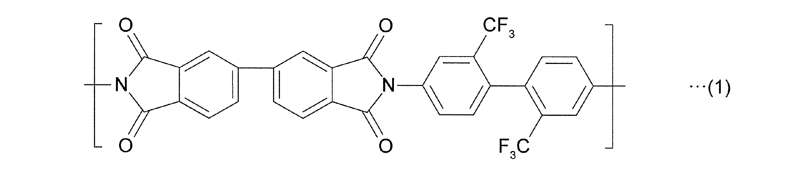
ポリイミドが式(1)で示される構造単位を含む場合には、耐熱性に優れながら、低い吸湿膨張係数を確保して、実装基板1の反りを抑制することができる。
より具体的には、酸二無水物成分がBPDAを含有し、ジアミン成分がTFMBを含有する場合には、下記式(2)で示される構造単位を含む。
式(2):
式(2):

(式中、xは、15以上、80以下である。)
xは、好ましくは、20以上、また、好ましくは、50以下である。
xは、好ましくは、20以上、また、好ましくは、50以下である。
xが、上記した下限以上であれば、低い吸湿膨張係数を確保することができる。xが、上記した上限以下であれば、ワニスを調製する際に、溶剤に容易に溶解させることができる。
絶縁材料の吸湿膨張係数は、15×10-6/%RH以下、好ましくは、13×10-6/%RH以下であり、また、例えば、0×10-6/%RH以上、好ましくは、1×10-6/%RH以上である。
絶縁材料の吸湿膨張係数が上記した上限を超えれば、ベース絶縁層4の反り、ひいては、実装基板1の反りを抑制することができない。一方、絶縁材料の吸湿膨張係数が上記した上限以下であれば、ベース絶縁層4の反りを抑制し、ひいては、実装基板1の反りを抑制することができる。
ベース絶縁層4を形成するための絶縁材料の吸湿膨張係数は、例えば、実装基板1における硬化後のベース絶縁層4の吸湿膨張係数と同一である。
絶縁材料の吸湿膨張係数は、特開2013-100441号公報の実施例の記載に従って測定される。
ベース絶縁層4の厚みT1は、例えば、12μm以下、好ましくは、8μm以下であり、また、例えば、1μm以上、好ましくは、3μm以上である。なお、ベース絶縁層4の厚みT1は、後述するベース絶縁層4の厚みT1およびカバー絶縁層6の厚みT2の総計が所望範囲となるように、調整される。
導体パターン5は、ベース絶縁層4の上面と接触するように、ベース絶縁層4の上側に設けられている。導体パターン5は、複数の撮像素子接続端子10、複数の外部部品接続端子11(図2参照)、および、複数の配線9を備える。
複数の撮像素子接続端子10は、図1に示すように、ハウジング配置部2の中央部に、矩形枠状となるように、互いに間隔を隔てて整列配置されている。すなわち、複数の撮像素子接続端子10は、図2に示すように、実装される撮像素子21の複数の端子25(図4参照)に対応するように、設けられている。また、複数の撮像素子接続端子10は、複数の撮像素子開口部7に対応して設けられている。撮像素子接続端子10は、底面視略円形状を有している。撮像素子接続端子10は、断面視(側断面視および正断面視)において、下側に凸となるように形成されている。具体的には、撮像素子接続端子10は、撮像素子開口部7の外周に配置される外周部12と、外周部12から内側に窪むように撮像素子開口部7内に配置される内側部13とを一体的に備える。内側部13の下面(露出面)は、撮像素子開口部7から露出しており、平坦となるように形成されている。また、内側部13の下面は、ベース絶縁層4の下面と面一となるように形成されている。
複数の外部部品接続端子11は、図1に示すように、外部部品接続部3の後端縁に、左右方向に互いに間隔を隔てて整列配置されている。すなわち、外部部品の複数の端子(図示せず)と対応するように設けられている。また、複数の外部部品接続端子11は、複数の外部部品開口部8に対応して設けられている。外部部品接続端子11は、平面視略矩形状(長方形状)を有している。外部部品接続端子11は、外部部品開口部8内に配置され、その下面は、外部部品開口部8から露出している。
複数の配線9は、図2に示すように、複数の接続配線14および複数のグランド配線15を備える。
複数の接続配線14は、複数の撮像素子接続端子10および複数の外部部品接続端子11に対応するように設けられている。具体的には、接続配線14は、図1において図示しないが、撮像素子接続端子10と外部部品接続端子11とを接続するように、これらと一体的に形成されている。すなわち、接続配線14の一端は、撮像素子接続端子10と連続し、接続配線14の他端は、外部部品接続端子11と連続して、これらを電気的に接続している。
複数のグランド配線15は、複数の接続配線14に対応するように設けられている。具体的には、複数のグランド配線15は、複数の接続配線14の外側に、これらに沿うように設けられている。グランド配線15の一端には、図示しないグランド端子が一体的に接続されている。
導体パターン5の材料としては、例えば、銅、銀、金、ニッケルまたはそれらを含む合金、半田などの金属材料が挙げられる。好ましくは、銅が挙げられる。
導体パターン5の厚みは、例えば、1μm以上、好ましくは、3μm以上であり、また、例えば、15μm以下、好ましくは、10μm以下である。配線9の幅は、例えば、5μm以上、好ましくは、10μm以上であり、また、例えば、100μm以下、好ましくは、50μm以下である。
カバー絶縁層6は、図2に示すように、導体パターン5を被覆するように、ベース絶縁層4および導体パターン5の上側に設けられている。すなわち、カバー絶縁層6は、導体パターン5の上面および側面、および、導体パターン5から露出するベース絶縁層4の上面と接触するように、配置されている。カバー絶縁層6は、実装基板1の上層を形成する。カバー絶縁層6の外形は、外部部品接続端子11の形成部分を除いて、ベース絶縁層4と同一となるように形成されている。
カバー絶縁層6は、ベース絶縁層4で上記した絶縁材料と同様の絶縁材料を含有する。
カバー絶縁層6を形成するための絶縁材料の吸湿膨張係数は、例えば、ベース絶縁層4を形成するための絶縁材料の吸湿膨張係数と同一である。絶縁材料の吸湿膨張係数は、特開2013-100441号公報の実施例の記載に従って測定される。具体的には、カバー絶縁層6を形成するための絶縁材料の吸湿膨張係数は、15×10-6/%RH以下、好ましくは、13×10-6/%RH以下であり、また、例えば、0×10-6/%RH以上、好ましくは、1×10-6/%RH以上である。絶縁材料の吸湿膨張係数が上記した上限を超えれば、カバー絶縁層6の反り、ひいては、実装基板1の反りを抑制することができない。一方、絶縁材料の吸湿膨張係数が上記した上限以下であれば、カバー絶縁層6の反りを抑制し、ひいては、実装基板1の反りを抑制することができる。
カバー絶縁層6の厚みT2は、例えば、6μm以下、好ましくは、4μm以下であり、また、例えば、1μm以上、好ましくは、2μm以上である。
なお、カバー絶縁層6の厚みT2は、次に説明するベース絶縁層4の厚みT1およびカバー絶縁層6の厚みT2の総計が所望範囲となるように、調整される。
ベース絶縁層4の厚みT1およびカバー絶縁層6の厚みT2の総計(絶縁層の総厚み、T1+T2)は、16μm以下、好ましくは、13μm以下、より好ましくは、10μm以下であり、また、例えば、1μm以上、好ましくは、5μm以上である。なお、ベース絶縁層4およびカバー絶縁層6の総厚みは、導体パターン5が形成されていない領域において、厚み方向において互いに接触するベース絶縁層4およびカバー絶縁層6の厚みである。
ベース絶縁層4およびカバー絶縁層6の総厚みが上記した上限を超えれば、実装基板1が反り易いという不具合(本発明の課題)を生じない。
一方、ベース絶縁層4およびカバー絶縁層6の総厚みが上記した上限以下であれば、実装基板1が反り易くなるという不具合(本発明の課題)を生じる。しかし、ベース絶縁層4の下面の全てが下方に露出し、かつ、ベース絶縁層4は、15×10-6/%RH以下の吸湿膨張係数を有する絶縁材料を含有するので、実装基板1の反りを抑制することができる。
ベース絶縁層4の厚みT1のカバー絶縁層6の厚みT2に対する比(T1/T2)は、例えば、5以下、好ましくは、1.8以下であり、また、例えば、1以上、好ましくは、1.3以上である。
実装基板1の厚み(ベース絶縁層4、導体パターン5およびカバー絶縁層6の総厚み)は、例えば、50μm以下、好ましくは、30μm以下、より好ましくは、20μm以下であり、また、例えば、1μm以上、好ましくは、5μm以上である。
2.撮像素子実装基板の製造方法
実装基板1は、図3A~図3Dに示すように、例えば、金属支持体用意工程、ベース絶縁層形成工程、導体パターン形成工程、カバー絶縁層形成工程、および、金属支持体除去工程を順に実施することにより、得られる。
実装基板1は、図3A~図3Dに示すように、例えば、金属支持体用意工程、ベース絶縁層形成工程、導体パターン形成工程、カバー絶縁層形成工程、および、金属支持体除去工程を順に実施することにより、得られる。
図3Aに示すように、金属支持体用意工程では、金属支持体19を用意する。
金属支持体19は、面方向に延びる平面視略矩形(長方形状)の平板形状(シート形状)を有する。
金属支持体19は、例えば、ステンレス、42アロイ、アルミニウムなどの金属材料から形成されている。好ましくは、ステンレスから形成されている。
金属支持体19の厚みは、例えば、5μm以上、好ましくは、10μm以上であり、例えば、50μm以下、好ましくは、30μm以下である。
金属支持体19の上面は、平坦(平滑)となるように形成されている。
続いて、ベース絶縁層形成工程では、ベース絶縁層4を、金属支持体19の上面に形成する。すなわち、撮像素子開口部7および外部部品開口部8を有するベース絶縁層4を、金属支持体19の上面に形成する。
具体的には、まず、感光性の絶縁材料のワニスを調製する。絶縁材料がポリイミドであれば、ワニスは、上記した酸二無水物成分とジアミンとを溶解できる溶剤を適宜の割合で含有することができ、さらには、感光剤、増感剤、重合停止剤、連鎖移動剤、レベリング剤、可塑剤、界面活性剤、消泡剤などの添加剤を適宜の割合で含有することができる。
続いて、ワニスを金属支持体19の上面全面に塗布して、次いで、溶剤を乾燥させる。これによって、ベース皮膜を形成する。その後、ベース皮膜を、撮像素子開口部7および外部部品開口部8に対応するパターンを有するフォトマスクを介して露光する。その後、ベース皮膜を現像し、その後、必要により加熱硬化させる。
図3Bに示すように、導体パターン形成工程では、導体パターン5を、上記したパターンで、ベース絶縁層4の上面と、撮像素子開口部7および外部部品開口部8から露出する実装基板1の上面とに、形成する。導体パターン5を、例えば、アディティブ法などによって、形成する。
図3Cに示すように、カバー絶縁層形成工程では、カバー絶縁層6を、導体パターン5およびベース絶縁層4の上面に配置する。カバー絶縁層形成工程は、ベース絶縁層形成工程と同様に実施する。
これにより、ベース絶縁層4と、導体パターン5と、カバー絶縁層6とを備える実装基板1を、金属支持体19に支持された状態で得る。なお、この実装基板1は、金属支持体19を備え、未だ除去されていない。そのため、この実装基板1は、本発明のフレキシブル配線回路基板に包含されない。
図3Dに示すように、金属支持体除去工程では、金属支持体19を除去する。
金属支持体19の除去方法としては、例えば、金属支持体19を、ベース絶縁層4の下面と、撮像素子開口部7から露出する撮像素子接続端子10の下面および外部部品開口部8から露出する外部部品接続端子11の下面とから剥離する方法、例えば、金属支持体19に対して、例えば、ドライエッチング、ウェットエッチングなどのエッチングを施す方法などが挙げられる。好ましくは、エッチング、より好ましくは、ウエットエッチングが挙げられる。ウエットエッチングでは、塩化第二鉄水溶液などをエッチング液として用いて、スプレーまたは浸漬する化学エッチング法が挙げられる。
これにより、金属支持体19が除去され、ベース絶縁層4と、導体パターン5と、カバー絶縁層6とを備える実装基板1を得る。実装基板1は、金属支持体19を備えず、好ましくは、ベース絶縁層4と、導体パターン5と、カバー絶縁層6とのみからなる。この実装基板1は、金属支持体19が除去されることによって、次に説明する用途に用いることができるとともに、作用効果を奏することができる。
このような実装基板1は、例えば、撮像素子を実装するための撮像素子実装基板に用いられる。すなわち、実装基板1は、カメラモジュールなどの撮像装置に備えられる。なお、実装基板1は、次に説明する撮像装置ではなく、撮像装置の一部品、すなわち、撮像装置を作製するための部品であり、撮像素子を含まず、具体的には、部品単独で流通し、産業上利用可能なデバイスである。
3.撮像装置
次に、本発明の撮像装置の一例として、実装基板1を備える撮像装置20を説明する。
次に、本発明の撮像装置の一例として、実装基板1を備える撮像装置20を説明する。
図4に示すように、撮像装置20は、実装基板1、撮像素子21、ハウジング22、光学レンズ23、および、フィルター24を備える。
実装基板1は、図2に示される実装基板1を上下反転して撮像装置20に備えられる。すなわち、実装基板1は、ベース絶縁層4を上側(厚み方向他方側)とし、カバー絶縁層6を下側(厚み方向一方側)となるように、配置される。
撮像素子21は、光を電気信号に変換する半導体素子であって、例えば、CMOSセンサ、CCDセンサなどの固体撮像素子が挙げられる。撮像素子21は、平面視略矩形の平板形状に形成されており、図示しないが、Si基板などのシリコンと、その上に配置されるフォトダイオード(光電変換素子)およびカラーフィルターとを備える。撮像素子21の下面には、実装基板1の撮像素子接続端子10と対応する端子25が複数設けられている。撮像素子21の厚みは、例えば、10μm以上、好ましくは、50μm以上であり、また、例えば、1000μm以下、好ましくは、500μm以下である。
撮像素子21は、実装基板1に実装されている。具体的には、撮像素子21の端子25は、対応する実装基板1の撮像素子接続端子10と、ソルダーバンプ26などを介して、フリップチップ実装されている。これにより、撮像素子21は、実装基板1のハウジング配置部2の中央部に配置され、実装基板1の撮像素子接続端子10および外部部品接続端子11と電気的に接続されている。
撮像素子21は、実装基板1に実装されることにより、撮像ユニット27を構成する。すなわち、撮像ユニット27は、実装基板1と、それに実装される撮像素子21とを備える。
ハウジング22は、撮像素子21のハウジング配置部2に、撮像素子21と間隔を隔てて囲むように、配置されている。ハウジング22は、平面視略矩形状の筒状を有している。ハウジング22の上端には、光学レンズ23を固定するための固定部が設けられている。
光学レンズ23は、実装基板1の上側に、実装基板1および撮像素子21と間隔を隔てて配置されている。光学レンズ23は、平面視略円形状に形成され、外部からの光が、撮像素子21に到達するように、固定部によって固定されている。
フィルター24は、撮像素子21および光学レンズ23の上下方向中央に、これらと間隔を隔てて配置され、ハウジング22に固定されている。
そして、この実装基板1では、ベース絶縁層4およびカバー絶縁層6の総厚み(T1+T2)が、16μm以下と薄いので、薄型化を図ることができる。
また、この実装基板1では、図2に示すように、ベース絶縁層4の下面の全ては、下方に向かって露出し、かつ、ベース絶縁層4は、15×10-6/%RH以下の低い吸湿膨張係数を有する絶縁材料を含有するので、反りを抑制することができる。
とりわけ、実装基板1が金属支持体19を備える場合において、ベース絶縁層4およびカバー絶縁層6の総厚みが、金属支持体19の厚みに対して薄い場合には、金属支持体19の剛性がベース絶縁層4およびカバー絶縁層6を過度に拘束し、却って、反りの不具合が顕在化される。しかし、この一実施形態では、ベース絶縁層4の下面の全ては、下方に向かって露出している(実装基板1に金属支持体19が備えられない)ため、ベース絶縁層4およびカバー絶縁層6を金属支持体19の拘束から解放することができる。また、これにより、ベース絶縁層4の下面の全ては、露出されるが、ベース絶縁層4は、低い吸湿膨張係数を有する絶縁材料からなるので、それらの総厚みが薄くても、湿度の影響を受けにくく、よって、反りを抑制することができる。
さらに、絶縁材料は、式(1)で示される構造単位を含むポリイミドであれば、耐熱性に優れながら、低い吸湿膨張係数を確保して、実装基板1の反りを抑制することができる。
また、この実装基板1では、導体パターン5は、ベース絶縁層4から下方に露出する撮像素子接続端子10および外部部品接続端子11を備えるので、それらを撮像素子21および外部部品と確実に電気的に接続することができる。
また、この実装基板1は、撮像素子21を実装する撮像素子実装基板1であるので、薄型化が図られた撮像装置を提供することができるとともに、実装基板1の反りが抑制されている。そのため、撮像装置20では、実装基板1と撮像素子21との接続信頼性を向上させることができる。
上記した図3A~図3Dに示す実装基板1の製造方法によれば、薄型化が図られ、反りが抑制された実装基板1を得ることができる。
<変形例>
変形例において、一実施形態と同様の部材および工程については、同一の参照符号を付し、その詳細な説明を省略する。
変形例において、一実施形態と同様の部材および工程については、同一の参照符号を付し、その詳細な説明を省略する。
一実施形態では、カバー絶縁層6を形成するための絶縁材料の吸湿膨張係数を、ベース絶縁層4を形成するための絶縁材料の吸湿膨張係数と同一に設定しているが、これに限定されず、例えば、カバー絶縁層6を形成するための絶縁材料の吸湿膨張係数を、ベース絶縁層4を形成するための絶縁材料の吸湿膨張係数の範囲外であってもよい。要するに、少なくともベース絶縁層4を形成するための絶縁材料が、所望の吸湿膨張係数であれば、よい。
一実施形態では、本発明のフレキシブル配線回路基板として、撮像素子21を実装するための撮像素子実装基板1(実装基板1)として説明しているが、フレキシブル配線回路基板の用途は、これに限定されない。例えば、薄型化および反りの抑制が要求される各種用途、具体的には、圧力センサ、加速度センサ、ジャイロセンサ、超音波センサ、指紋認証センサなどの実装基板などに好適に用いられる。
一実施形態の実装基板1では、図2に示すように、配線9は、グランド配線15を備えるが、例えば、図示しないが、グランド配線15を備えなくてもよい。すなわち、配線9を、接続配線14のみから構成することもできる。
また、一実施形態の撮像装置20では、図4に示すように、撮像素子21は、実装基板1にフリップチップ実装されているが、例えば、図示しないが、撮像素子21は、実装基板1にワイヤボンディングによって実装することもできる。
一実施形態では、図2に示すように、実装基板1は、ベース絶縁層4、導体パターン5およびカバー絶縁層6のみを備えるが、例えば、この変形例では、図5に示すように、実装基板1は、シールド層40、および、第3絶縁層の一例としての第2カバー絶縁層31をさらに備える。
この実装基板1は、ベース絶縁層4と、導体パターン5と、カバー絶縁層(第1カバー絶縁層)6と、シールド層40と、第2カバー絶縁層31とを、上側に向かって順に備える。
シールド層40は、カバー絶縁層6の上面と接触するように、カバー絶縁層6の上側に配置されている。シールド層40は、外部からの電磁波を遮蔽する層であって、面方向(前後方向および左右方向)に延びるシート状に形成されている。
シールド層40は、グランド配線15と電気的に接続されている。すなわち、シールド層40は、グランド配線15と連続している。具体的には、シールド層40は、グランド配線15と対向する部分において、下側に凸形状を有し、グランド配線15の上面に接触する接触部41を備える。
接触部41は、グランド配線15に直接接触する平坦部42と、平坦部42の周囲に連続するように一体的に配置される傾斜部43とを備える。
平坦部42は、面方向に延びる平板状に形成されている。傾斜部43は、上下方向および面方向に交差(傾斜)する傾斜方向に延びている。
これにより、シールド層40は、グランド配線15を介して、接地されている。
シールド層40は、導体からなり、例えば、銅、クロム、ニッケル、金、銀、白金、パラジウム、チタン、タンタル、はんだ、またはこれらの合金などの金属材料が用いられる。好ましくは、銅が挙げられる。シールド層40の厚みは、例えば、0.05μm以上、好ましくは、0.1μm以上であり、また、例えば、3μm以下、好ましくは、1μm以下である。
第2カバー絶縁層31は、シールド層40を被覆するように、シールド層40の上側に設けられている。第2カバー絶縁層31の外形は、カバー絶縁層6と同一となるように形成されている。
第2カバー絶縁層31は、ベース絶縁層4で上記した絶縁材料と同様の絶縁材料を含有する。第2カバー絶縁層31を形成するための絶縁材料の吸湿膨張係数は、ベース絶縁層4を形成するための絶縁材料の吸湿膨張係数と同一である。具体的には、第2カバー絶縁層31を形成するための絶縁材料の吸湿膨張係数は、15×10-6/%RH以下、好ましくは、13×10-6/%RH以下であり、また、例えば、0×10-6/%RH以上、好ましくは、1×10-6/%RH以上である。絶縁材料の吸湿膨張係数が上記した上限を超えれば、第2カバー絶縁層31の反り、ひいては、実装基板1の反りを抑制することができない。一方、絶縁材料の吸湿膨張係数が上記した上限以下であれば、第2カバー絶縁層31の反りを抑制し、ひいては、実装基板1の反りを抑制することができる。
第2カバー絶縁層31の厚みT3は、例えば、3μm以下、好ましくは、2μm以下であり、また、例えば、0.1μm以上、好ましくは、1μm以上である。
ベース絶縁層4の厚みT1、カバー絶縁層6の厚みT2および第2カバー絶縁層31の厚みT3の総計(絶縁層の総厚み、T1+T2+T3)は、16μm以下、好ましくは、13μm以下、より好ましくは、10μm以下であり、また、例えば、1μm以上、好ましくは、5μm以上である。ベース絶縁層4、カバー絶縁層6および第2カバー絶縁層31の総厚みが上記した上限以下であれば、第2カバー絶縁層31の反りを抑制できる。
さらに、第2カバー絶縁層31は、15×10-6/%RH以下の吸湿膨張係数を有する絶縁材料を含有する。
図5に示す実装基板1は、一実施形態の実装基板1を金属支持体19で支持された状態で得た後に、シールド層40および第2カバー絶縁層31をこの順で、第1カバー絶縁層6の上面に形成し、続いて、金属支持体19を除去することにより、製造することができる。
また、図2において図示しないが、導体パターン5の一部が、カバー絶縁層6から露出することもできる。
さらに、図6Aに示すように、複数の実装基板1を基板集合体シート50として構成することもできる。基板集合体シート50は、面方向において整列状態の、複数の実装基板1を備える。
上記した各変形例についても、一実施形態と同様の作用効果を奏する。
以下に製造例、比較製造例、実施例および比較例を示し、本発明をさらに具体的に説明する。なお、本発明は、何ら製造例、比較製造例、実施例および比較例に限定されない。また、以下の記載において用いられる配合割合(含有割合)、物性値、パラメータなどの具体的数値は、上記の「発明を実施するための形態」において記載されている、それらに対応する配合割合(含有割合)、物性値、パラメータなど該当記載の上限(「以下」、「未満」として定義されている数値)または下限(「以上」、「超過」として定義されている数値)に代替することができる。
製造例1
2,2’-ビス(トリフルオロメチル)-4,4’-ジアミノビフェニル(TFMB、ハロアルキル基を置換基として有する芳香族ジアミン)4.0g(20mmol)とp-フェニレンジアミン(PPD、芳香族ジアミン)8.65g(80mmol)とを500mlのセパラブルフラスコに投入し、200gの脱水されたN-メチル-2-ピロリドン(NMP)に溶解させ窒素気流下、オイルバスによって液温が50℃になるように熱電対でモニターし加熱しながら撹拌した。それらが完全に溶解したことを確認した後、そこへ、30分かけて3,3’、4,4’-ビフェニルテトラカルボン酸二無水物(BPDA、芳香族酸二無水物)29.4g(100mmol)をセパラブルフラスコに配合した後、50℃で5時間撹拌した、その後室温まで冷却し、ポリイミド前駆体溶液Aを得た。
2,2’-ビス(トリフルオロメチル)-4,4’-ジアミノビフェニル(TFMB、ハロアルキル基を置換基として有する芳香族ジアミン)4.0g(20mmol)とp-フェニレンジアミン(PPD、芳香族ジアミン)8.65g(80mmol)とを500mlのセパラブルフラスコに投入し、200gの脱水されたN-メチル-2-ピロリドン(NMP)に溶解させ窒素気流下、オイルバスによって液温が50℃になるように熱電対でモニターし加熱しながら撹拌した。それらが完全に溶解したことを確認した後、そこへ、30分かけて3,3’、4,4’-ビフェニルテトラカルボン酸二無水物(BPDA、芳香族酸二無水物)29.4g(100mmol)をセパラブルフラスコに配合した後、50℃で5時間撹拌した、その後室温まで冷却し、ポリイミド前駆体溶液Aを得た。
続いて、ポリイミド前駆体溶液Aの固形分100質量部に対して、ニフェジピン(感光剤)30質量部を配合して、感光性ポリイミド前駆体溶液Aを調製した。
比較製造例1
2,2’-ビス(トリフルオロメチル)-4,4’-ジアミノビフェニル(TFMB)4.0g(20mmol)とp-フェニレンジアミン(PPD)8.65g(80mmol)とに代えて、4,4’-ジアミノジフェニルエーテル(ODA、4,4'-オキシビス(ベンゼンアミン)、芳香族ジアミン)3.0g(15mmol)とパラフェニレンジアミン(PPD、芳香族ジアミン)9.19g(85mmol)とに変更した以外は、製造例1と同様に処理して、ポリイミド前駆体溶液B、続いて、感光性ポリイミド前駆体溶液Bを調製した。
2,2’-ビス(トリフルオロメチル)-4,4’-ジアミノビフェニル(TFMB)4.0g(20mmol)とp-フェニレンジアミン(PPD)8.65g(80mmol)とに代えて、4,4’-ジアミノジフェニルエーテル(ODA、4,4'-オキシビス(ベンゼンアミン)、芳香族ジアミン)3.0g(15mmol)とパラフェニレンジアミン(PPD、芳香族ジアミン)9.19g(85mmol)とに変更した以外は、製造例1と同様に処理して、ポリイミド前駆体溶液B、続いて、感光性ポリイミド前駆体溶液Bを調製した。
実施例1
図3Aに示すように、厚み18μmのステンレスからなる金属支持体19を用意した。
図3Aに示すように、厚み18μmのステンレスからなる金属支持体19を用意した。
次いで、製造例1のポリイミド前駆体溶液Aを金属支持体19の上面に塗布し、次いで、80℃で10分乾燥させて、ベース皮膜(ポリイミド前駆体皮膜)を形成した。続いて、ベース皮膜を、フォトマスクを介して露光し、続いて、現像した。その後、窒素雰囲気下、360℃1時間、ベース皮膜を加熱する(硬化させる)ことにより、ポリイミドからなり、撮像素子開口部7および外部部品開口部8を有する厚み10μmのベース絶縁層4を形成した。
図3Bに示すように、その後、銅からなる厚み8μmの導体パターン5を、ベース絶縁層4の上面と、撮像素子開口部7および外部部品開口部8から露出する金属支持体19の上面に、アディティブ法で形成した。
図3Cに示すように、その後、製造例1のポリイミド前駆体溶液をベース絶縁層4および導体パターン5の上面に塗布し、次いで、80℃で10分乾燥させて、カバー皮膜(ポリイミド前駆体皮膜)を形成した。続いて、カバー皮膜を、フォトマスクを介して露光し、続いて、現像した。その後、窒素雰囲気下、360℃1時間、カバー皮膜を加熱することにより、ポリイミドからなる、厚み5μmのカバー絶縁層6を得た。
その後、図3Dに示すように、金属支持体19を、塩化第二鉄水溶液からなるエッチング液を下方からスプレーする化学エッチング法によって、除去した。これによって、ベース絶縁層4の下面の全てを露出させた。
これにより、下面の全てを露出するベース絶縁層4、導体パターン5およびカバー絶縁層6を順に備える実装基板1を得た。
なお、ベース絶縁層4およびカバー絶縁層6のポリイミドは、ともに、式(2)に示す構造単位を有する。
式(2):
式(2):
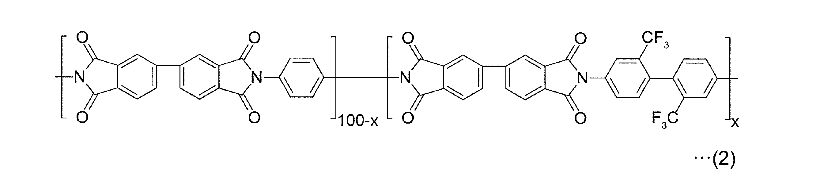
(式中、xは、20である。)
実施例2、3および比較例1
各層の処方、厚み、加熱温度等を表1に記載に基づいて変更した以外は、実施例1と同様にして、実装基板1を得た。
実施例2、3および比較例1
各層の処方、厚み、加熱温度等を表1に記載に基づいて変更した以外は、実施例1と同様にして、実装基板1を得た。
但し、比較例1のベース絶縁層4およびカバー絶縁層6のポリイミドは、ともに、下記式(3)に示す構造単位を有する。
式(3):
式(3):
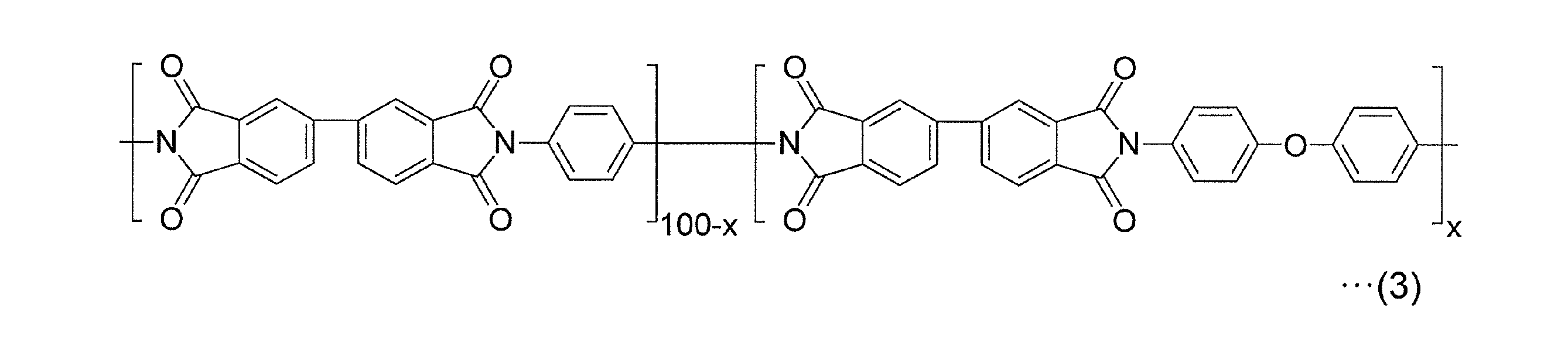
(式中、xは、15である。)
実施例4
ベース絶縁層4、導体パターン5、カバー絶縁層6、シールド層40および第2カバー絶縁層31を順に備える実装基板1を得た。
実施例4
ベース絶縁層4、導体パターン5、カバー絶縁層6、シールド層40および第2カバー絶縁層31を順に備える実装基板1を得た。
ベース絶縁層4、導体パターン5およびカバー絶縁層6は、実施例3と同様にして形成した。
スパッタによって、厚み0.1μmの銅からなるシールド層40を形成し、続いて、
ベース絶縁層4と同様にして、厚み2μmのポリイミドから第2カバー絶縁層31を形成した。
ベース絶縁層4と同様にして、厚み2μmのポリイミドから第2カバー絶縁層31を形成した。
比較例2
金属支持体19を除去させず、金属支持体19を備える実装基板1を製造した以外は、実施例2と同様に処理した。
金属支持体19を除去させず、金属支持体19を備える実装基板1を製造した以外は、実施例2と同様に処理した。
この実装基板1において、ベース絶縁層4の下面の全ては、金属支持体19によって被覆されている。
比較例3
金属支持体19を除去させず、金属支持体19を備える実装基板1を製造した以外は、比較例1と同様に処理した。
金属支持体19を除去させず、金属支持体19を備える実装基板1を製造した以外は、比較例1と同様に処理した。
この実装基板1において、ベース絶縁層4の下面の全ては、金属支持体19によって被覆されている。
各実施例および各比較例の層構成および厚みを表1に記載する。
[評価]
各実施例および各比較例の実装基板1について、以下の項目を評価した。その結果を表1に記載する。
各実施例および各比較例の実装基板1について、以下の項目を評価した。その結果を表1に記載する。
<湿度膨張係数>
各実施例および各比較例の実装基板1のベース絶縁層4およびカバー絶縁層6の湿度膨張係数を測定した。
各実施例および各比較例の実装基板1のベース絶縁層4およびカバー絶縁層6の湿度膨張係数を測定した。
具体的には、まず、実装基板1のベース絶縁層4およびカバー絶縁層6の積層部分を試料として採取した。
続いて、試料を充分に乾燥させ、その後、試料を、湿度型熱機械分析装置(HC-TMA4000SA、ブルカー・エイエックスエス社製)のチャンバー内30℃で5%RHの環境下にて3時間保持させて安定させた後、試料に荷重(196mN)を負荷し、続いて、相対湿度を75%RHに変化させ、3時間保持させて安定させた。そして、湿度型熱機械分析装置の演算処理によって、吸湿膨張係数を、試料伸びと相対湿度の変化量(70%RH)とから取得した。
<反り>
実装基板1の反りを測定した。
実装基板1の反りを測定した。
具体的には、図6Aに示すように、まず、9個の実装基板1を備える基板集合体シート50を用意した。各実装基板1の外形サイズは、15mm×15mmであり、また、基板集合体シート50の外形サイズは、45mm×45mmであった。
続いて、基板集合体シート50を、温度25℃、湿度60%RHの環境下において、平板45の表面に載置した。
24時間経過後、図6Bに示すように、基板集合体シート50の4つの頂点における各下端部と、平板45の表面との高さ(h1、h2、h3、h4)を測定し、それらの平均値([h1+h2+h3+h4]/4)を反りとして算出した。
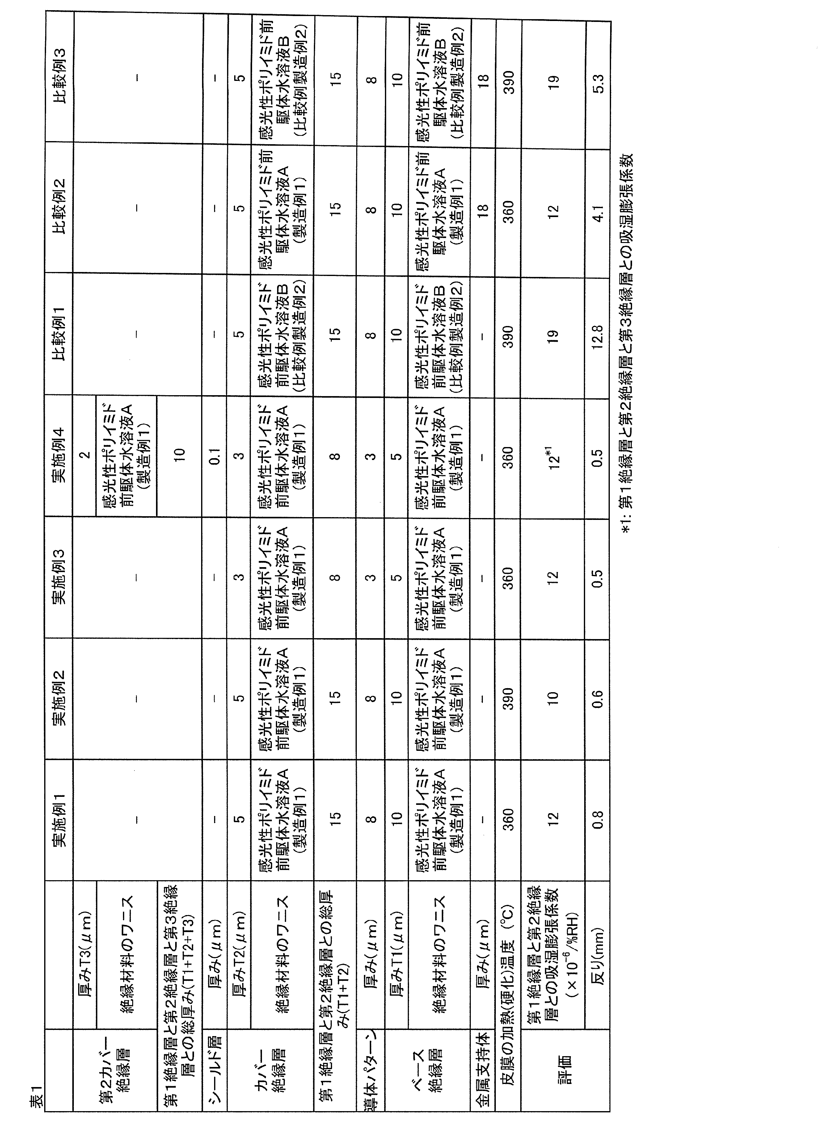
なお、上記発明は、本発明の例示の実施形態として提供したが、これは単なる例示に過ぎず、限定的に解釈してはならない。当該技術分野の当業者によって明らかなら本発明の変形例は、後記請求の範囲に含まれる。
フレキシブル配線回路基板は、撮像装置に備えられる。
1 実装基板(撮像素子実装基板)
4 ベース絶縁層
5 導体パターン
6 カバー絶縁層
10 撮像素子接続端子
11 外部部品接続端子
20 撮像装置
21 撮像素子
31 第2カバー絶縁層
40 シールド層
50 基板集合体シート
T1 ベース絶縁層の厚み
T2 カバー絶縁層の厚み
T3 第2カバー絶縁層の厚み
4 ベース絶縁層
5 導体パターン
6 カバー絶縁層
10 撮像素子接続端子
11 外部部品接続端子
20 撮像装置
21 撮像素子
31 第2カバー絶縁層
40 シールド層
50 基板集合体シート
T1 ベース絶縁層の厚み
T2 カバー絶縁層の厚み
T3 第2カバー絶縁層の厚み
Claims (9)
- 第1絶縁層と、導体パターンと、第2絶縁層とを厚み方向一方側に向かって順に備え、
前記第1絶縁層の厚み方向他方面の全ては、厚み方向他方側に向かって露出し、
前記第1絶縁層および前記第2絶縁層の総厚みが、16μm以下であり、
少なくとも前記第1絶縁層は、15×10-6/%RH以下の吸湿膨張係数を有する絶縁材料を含有することを特徴とする、フレキシブル配線回路基板。 - 前記絶縁材料は、下記式(1)で示される構造単位を含むポリイミドであることを特徴とする、請求項1に記載のフレキシブル配線回路基板。
式(1):

- 前記導体パターンは、前記第1絶縁層から厚み方向他方側に露出する端子を有することを特徴とする、請求項1に記載のフレキシブル配線回路基板。
- 前記導体パターンの一部は、前記第2絶縁層から厚み方向一方側に露出することを特徴とする、請求項1に記載のフレキシブル配線回路基板。
- シールド層と、第3絶縁層とをさらに備え、
前記第1絶縁層と、前記導体パターンと、前記第2絶縁層と、前記シールド層と、前記第3絶縁層とを、厚み方向一方側に向かって順に備え、
前記第1絶縁層、前記第2絶縁層および前記第3絶縁層の総厚みが、16μm以下であることを特徴とする、請求項1に記載のフレキシブル配線回路基板。 - 前記第3絶縁層は、15×10-6/%RH以下の吸湿膨張係数を有する絶縁材料を含有することを特徴とする、請求項5に記載のフレキシブル配線回路基板。
- 撮像素子を実装するための撮像素子実装基板であることを特徴とする、請求項1に記載のフレキシブル配線回路基板。
- 請求項7に記載される撮像素子実装基板と、
前記撮像素子実装基板に実装される撮像素子と
を備えることを特徴とする、撮像装置。 - 請求項1に記載のフレキシブル配線回路基板の製造方法であって、
金属支持基板を用意する工程、
前記金属支持基板の厚み方向一方側に、第1絶縁層と、導体パターンと、第2絶縁層とを順に形成する工程、および、
前記金属支持基板を除去する工程
を備えることを特徴とする、フレキシブル配線回路基板の製造方法。
Priority Applications (3)
| Application Number | Priority Date | Filing Date | Title |
|---|---|---|---|
| KR1020197031449A KR102548537B1 (ko) | 2017-04-28 | 2018-04-25 | 플렉시블 배선 회로 기판, 그의 제조 방법 및 촬상 장치 |
| US16/607,616 US10813221B2 (en) | 2017-04-28 | 2018-04-25 | Flexible wiring circuit board, producing method thereof, and imaging device |
| CN201880027870.4A CN110547052B (zh) | 2017-04-28 | 2018-04-25 | 柔性布线电路基板、其制造方法及成像装置 |
Applications Claiming Priority (2)
| Application Number | Priority Date | Filing Date | Title |
|---|---|---|---|
| JP2017-090243 | 2017-04-28 | ||
| JP2017090243A JP6990987B2 (ja) | 2017-04-28 | 2017-04-28 | フレキシブル配線回路基板、その製造方法および撮像装置 |
Publications (1)
| Publication Number | Publication Date |
|---|---|
| WO2018199129A1 true WO2018199129A1 (ja) | 2018-11-01 |
Family
ID=63919125
Family Applications (1)
| Application Number | Title | Priority Date | Filing Date |
|---|---|---|---|
| PCT/JP2018/016723 Ceased WO2018199129A1 (ja) | 2017-04-28 | 2018-04-25 | フレキシブル配線回路基板、その製造方法および撮像装置 |
Country Status (6)
| Country | Link |
|---|---|
| US (1) | US10813221B2 (ja) |
| JP (1) | JP6990987B2 (ja) |
| KR (1) | KR102548537B1 (ja) |
| CN (1) | CN110547052B (ja) |
| TW (1) | TWI763835B (ja) |
| WO (1) | WO2018199129A1 (ja) |
Cited By (2)
| Publication number | Priority date | Publication date | Assignee | Title |
|---|---|---|---|---|
| WO2021005864A1 (ja) * | 2019-07-09 | 2021-01-14 | 日東電工株式会社 | 配線回路基板および配線回路基板の製造方法 |
| WO2021005863A1 (ja) * | 2019-07-09 | 2021-01-14 | 日東電工株式会社 | 配線回路基板および配線回路基板の製造方法 |
Families Citing this family (1)
| Publication number | Priority date | Publication date | Assignee | Title |
|---|---|---|---|---|
| JP2020120106A (ja) * | 2019-01-23 | 2020-08-06 | キヤノン株式会社 | 電子モジュール、電子機器、撮像センサモジュール、撮像装置及び表示装置 |
Citations (3)
| Publication number | Priority date | Publication date | Assignee | Title |
|---|---|---|---|---|
| JPS62242384A (ja) * | 1986-04-14 | 1987-10-22 | 旭化成株式会社 | フレキシブル配線基板およびその製造方法 |
| JP2009184131A (ja) * | 2008-02-04 | 2009-08-20 | Nippon Steel Chem Co Ltd | 多層積層体及びフレキシブル銅張積層板の製造方法 |
| JP2013100441A (ja) * | 2011-11-10 | 2013-05-23 | Nitto Denko Corp | ポリイミド前駆体組成物およびそれを用いた配線回路基板 |
Family Cites Families (10)
| Publication number | Priority date | Publication date | Assignee | Title |
|---|---|---|---|---|
| JP2000133896A (ja) * | 1998-10-28 | 2000-05-12 | Olympus Optical Co Ltd | 配線板 |
| US7550194B2 (en) * | 2005-08-03 | 2009-06-23 | E. I. Du Pont De Nemours And Company | Low color polyimide compositions useful in optical type applications and methods and compositions relating thereto |
| KR20070058812A (ko) * | 2005-12-05 | 2007-06-11 | 주식회사 코오롱 | 폴리이미드 필름 |
| JP5099509B2 (ja) | 2007-05-11 | 2012-12-19 | 大日本印刷株式会社 | サスペンション用基板、その製造方法、磁気ヘッドサスペンションおよびハードディスクドライブ |
| JP5383343B2 (ja) * | 2008-06-26 | 2014-01-08 | 新日鉄住金化学株式会社 | 白色ポリイミドフィルム |
| JP5807369B2 (ja) * | 2010-04-19 | 2015-11-10 | 大日本印刷株式会社 | 回路基板、サスペンション用基板、サスペンション、素子付サスペンションおよびハードディスクドライブ |
| KR20140037650A (ko) * | 2012-09-19 | 2014-03-27 | 삼성전기주식회사 | 패키지 기판용 수지 조성물, 및 이를 코어 절연재와 프리프레그로 포함하는 패키지 기판 |
| JP6067419B2 (ja) * | 2013-02-28 | 2017-01-25 | 新日鉄住金化学株式会社 | 積層部材の製造方法 |
| JP2014172978A (ja) * | 2013-03-08 | 2014-09-22 | Sumitomo Bakelite Co Ltd | 共重合ポリイミド前駆体および共重合ポリイミド |
| JP2018181433A (ja) * | 2017-04-04 | 2018-11-15 | 株式会社ジャパンディスプレイ | 有機エレクトロルミネッセンス表示装置及びその製造方法 |
-
2017
- 2017-04-28 JP JP2017090243A patent/JP6990987B2/ja active Active
-
2018
- 2018-04-25 US US16/607,616 patent/US10813221B2/en active Active
- 2018-04-25 CN CN201880027870.4A patent/CN110547052B/zh active Active
- 2018-04-25 KR KR1020197031449A patent/KR102548537B1/ko active Active
- 2018-04-25 WO PCT/JP2018/016723 patent/WO2018199129A1/ja not_active Ceased
- 2018-04-27 TW TW107114436A patent/TWI763835B/zh active
Patent Citations (3)
| Publication number | Priority date | Publication date | Assignee | Title |
|---|---|---|---|---|
| JPS62242384A (ja) * | 1986-04-14 | 1987-10-22 | 旭化成株式会社 | フレキシブル配線基板およびその製造方法 |
| JP2009184131A (ja) * | 2008-02-04 | 2009-08-20 | Nippon Steel Chem Co Ltd | 多層積層体及びフレキシブル銅張積層板の製造方法 |
| JP2013100441A (ja) * | 2011-11-10 | 2013-05-23 | Nitto Denko Corp | ポリイミド前駆体組成物およびそれを用いた配線回路基板 |
Cited By (9)
| Publication number | Priority date | Publication date | Assignee | Title |
|---|---|---|---|---|
| WO2021005864A1 (ja) * | 2019-07-09 | 2021-01-14 | 日東電工株式会社 | 配線回路基板および配線回路基板の製造方法 |
| WO2021005863A1 (ja) * | 2019-07-09 | 2021-01-14 | 日東電工株式会社 | 配線回路基板および配線回路基板の製造方法 |
| JP2021012984A (ja) * | 2019-07-09 | 2021-02-04 | 日東電工株式会社 | 配線回路基板および配線回路基板の製造方法 |
| JP2021012983A (ja) * | 2019-07-09 | 2021-02-04 | 日東電工株式会社 | 配線回路基板および配線回路基板の製造方法 |
| CN114127141A (zh) * | 2019-07-09 | 2022-03-01 | 日东电工株式会社 | 布线电路基板、以及布线电路基板的制造方法 |
| JP7317604B2 (ja) | 2019-07-09 | 2023-07-31 | 日東電工株式会社 | 配線回路基板および配線回路基板の製造方法 |
| JP7325250B2 (ja) | 2019-07-09 | 2023-08-14 | 日東電工株式会社 | 配線回路基板および配線回路基板の製造方法 |
| TWI855060B (zh) * | 2019-07-09 | 2024-09-11 | 日商日東電工股份有限公司 | 配線電路基板及配線電路基板之製造方法 |
| TWI855061B (zh) * | 2019-07-09 | 2024-09-11 | 日商日東電工股份有限公司 | 配線電路基板及配線電路基板之製造方法 |
Also Published As
| Publication number | Publication date |
|---|---|
| JP6990987B2 (ja) | 2022-01-12 |
| US10813221B2 (en) | 2020-10-20 |
| CN110547052B (zh) | 2023-05-23 |
| TWI763835B (zh) | 2022-05-11 |
| US20200077520A1 (en) | 2020-03-05 |
| KR102548537B1 (ko) | 2023-06-27 |
| KR20200002848A (ko) | 2020-01-08 |
| JP2018190787A (ja) | 2018-11-29 |
| TW201907763A (zh) | 2019-02-16 |
| CN110547052A (zh) | 2019-12-06 |
Similar Documents
| Publication | Publication Date | Title |
|---|---|---|
| TWI501039B (zh) | 感光性樹脂組成物、感光性樹脂組成物薄膜及使用其之半導體裝置 | |
| CN102290054B (zh) | 悬浮臂用基板、其制备方法、磁头悬浮臂和硬盘驱动器 | |
| KR102515701B1 (ko) | 촬상 소자 실장 기판, 그 제조 방법 및 실장 기판 집합체 | |
| TWI763835B (zh) | 可撓配線電路基板、其製造方法及攝像裝置 | |
| US20180066107A1 (en) | Photosensitive resin composition | |
| KR100969014B1 (ko) | 포지티브형 감광성 수지 조성물 및 패턴 형성방법 | |
| JP7070406B2 (ja) | 樹脂組成物 | |
| JP6007510B2 (ja) | 感光性樹脂組成物、保護膜および半導体装置 | |
| JP7586944B2 (ja) | 撮像素子実装基板、その製造方法、および、実装基板集合体 | |
| JP3523952B2 (ja) | ポリイミド−金属箔複合フィルム | |
| JP5592740B2 (ja) | ハードディスクドライブのスライダ用回路付きサスペンション基板 | |
| TWI855060B (zh) | 配線電路基板及配線電路基板之製造方法 | |
| JP4178934B2 (ja) | 耐熱性積層フィルムおよび金属層付き積層フィルム、ならびにこれらを用いた半導体装置 | |
| JP6094137B2 (ja) | 回路基板、サスペンション用基板、サスペンション、素子付サスペンションおよびハードディスクドライブ | |
| JP5390964B2 (ja) | 感光性樹脂組成物及びそれを用いた感光性フィルム | |
| JP2001044583A (ja) | 回路基板、および回路基板の製造方法 | |
| JP5807369B2 (ja) | 回路基板、サスペンション用基板、サスペンション、素子付サスペンションおよびハードディスクドライブ | |
| JP2000096010A (ja) | 半導体装置用接着テープ | |
| WO2018199128A1 (ja) | フレキシブル配線回路基板および撮像装置 | |
| JP2000026722A (ja) | ポリイミド前駆体を含む樹脂組成物とポジ型感光性樹脂組成物およびそれを用いた電子装置とそのパターン形成方法 | |
| JP2006210482A (ja) | 光電子回路用プリント基板 |
Legal Events
| Date | Code | Title | Description |
|---|---|---|---|
| 121 | Ep: the epo has been informed by wipo that ep was designated in this application |
Ref document number: 18791561 Country of ref document: EP Kind code of ref document: A1 |
|
| ENP | Entry into the national phase |
Ref document number: 20197031449 Country of ref document: KR Kind code of ref document: A |
|
| NENP | Non-entry into the national phase |
Ref country code: DE |
|
| 122 | Ep: pct application non-entry in european phase |
Ref document number: 18791561 Country of ref document: EP Kind code of ref document: A1 |