WO2018181049A1 - El表示パネルの製造方法、el表示パネルの製造装置、el表示パネル、およびel表示装置 - Google Patents
El表示パネルの製造方法、el表示パネルの製造装置、el表示パネル、およびel表示装置 Download PDFInfo
- Publication number
- WO2018181049A1 WO2018181049A1 PCT/JP2018/011863 JP2018011863W WO2018181049A1 WO 2018181049 A1 WO2018181049 A1 WO 2018181049A1 JP 2018011863 W JP2018011863 W JP 2018011863W WO 2018181049 A1 WO2018181049 A1 WO 2018181049A1
- Authority
- WO
- WIPO (PCT)
- Prior art keywords
- emitting layer
- light emitting
- light
- pixel
- color
- Prior art date
Links
Images


Classifications
-
- H—ELECTRICITY
- H10—SEMICONDUCTOR DEVICES; ELECTRIC SOLID-STATE DEVICES NOT OTHERWISE PROVIDED FOR
- H10K—ORGANIC ELECTRIC SOLID-STATE DEVICES
- H10K59/00—Integrated devices, or assemblies of multiple devices, comprising at least one organic light-emitting element covered by group H10K50/00
- H10K59/30—Devices specially adapted for multicolour light emission
- H10K59/35—Devices specially adapted for multicolour light emission comprising red-green-blue [RGB] subpixels
-
- H—ELECTRICITY
- H10—SEMICONDUCTOR DEVICES; ELECTRIC SOLID-STATE DEVICES NOT OTHERWISE PROVIDED FOR
- H10K—ORGANIC ELECTRIC SOLID-STATE DEVICES
- H10K59/00—Integrated devices, or assemblies of multiple devices, comprising at least one organic light-emitting element covered by group H10K50/00
- H10K59/30—Devices specially adapted for multicolour light emission
-
- G—PHYSICS
- G09—EDUCATION; CRYPTOGRAPHY; DISPLAY; ADVERTISING; SEALS
- G09F—DISPLAYING; ADVERTISING; SIGNS; LABELS OR NAME-PLATES; SEALS
- G09F9/00—Indicating arrangements for variable information in which the information is built-up on a support by selection or combination of individual elements
- G09F9/30—Indicating arrangements for variable information in which the information is built-up on a support by selection or combination of individual elements in which the desired character or characters are formed by combining individual elements
-
- H—ELECTRICITY
- H05—ELECTRIC TECHNIQUES NOT OTHERWISE PROVIDED FOR
- H05B—ELECTRIC HEATING; ELECTRIC LIGHT SOURCES NOT OTHERWISE PROVIDED FOR; CIRCUIT ARRANGEMENTS FOR ELECTRIC LIGHT SOURCES, IN GENERAL
- H05B33/00—Electroluminescent light sources
- H05B33/10—Apparatus or processes specially adapted to the manufacture of electroluminescent light sources
-
- H—ELECTRICITY
- H10—SEMICONDUCTOR DEVICES; ELECTRIC SOLID-STATE DEVICES NOT OTHERWISE PROVIDED FOR
- H10K—ORGANIC ELECTRIC SOLID-STATE DEVICES
- H10K50/00—Organic light-emitting devices
- H10K50/10—OLEDs or polymer light-emitting diodes [PLED]
- H10K50/11—OLEDs or polymer light-emitting diodes [PLED] characterised by the electroluminescent [EL] layers
- H10K50/125—OLEDs or polymer light-emitting diodes [PLED] characterised by the electroluminescent [EL] layers specially adapted for multicolour light emission, e.g. for emitting white light
- H10K50/13—OLEDs or polymer light-emitting diodes [PLED] characterised by the electroluminescent [EL] layers specially adapted for multicolour light emission, e.g. for emitting white light comprising stacked EL layers within one EL unit
-
- H—ELECTRICITY
- H10—SEMICONDUCTOR DEVICES; ELECTRIC SOLID-STATE DEVICES NOT OTHERWISE PROVIDED FOR
- H10K—ORGANIC ELECTRIC SOLID-STATE DEVICES
- H10K50/00—Organic light-emitting devices
- H10K50/10—OLEDs or polymer light-emitting diodes [PLED]
- H10K50/14—Carrier transporting layers
- H10K50/15—Hole transporting layers
-
- H—ELECTRICITY
- H10—SEMICONDUCTOR DEVICES; ELECTRIC SOLID-STATE DEVICES NOT OTHERWISE PROVIDED FOR
- H10K—ORGANIC ELECTRIC SOLID-STATE DEVICES
- H10K50/00—Organic light-emitting devices
- H10K50/80—Constructional details
- H10K50/805—Electrodes
- H10K50/82—Cathodes
- H10K50/828—Transparent cathodes, e.g. comprising thin metal layers
-
- H—ELECTRICITY
- H10—SEMICONDUCTOR DEVICES; ELECTRIC SOLID-STATE DEVICES NOT OTHERWISE PROVIDED FOR
- H10K—ORGANIC ELECTRIC SOLID-STATE DEVICES
- H10K50/00—Organic light-emitting devices
- H10K50/80—Constructional details
- H10K50/85—Arrangements for extracting light from the devices
- H10K50/852—Arrangements for extracting light from the devices comprising a resonant cavity structure, e.g. Bragg reflector pair
-
- H—ELECTRICITY
- H10—SEMICONDUCTOR DEVICES; ELECTRIC SOLID-STATE DEVICES NOT OTHERWISE PROVIDED FOR
- H10K—ORGANIC ELECTRIC SOLID-STATE DEVICES
- H10K50/00—Organic light-emitting devices
- H10K50/80—Constructional details
- H10K50/85—Arrangements for extracting light from the devices
- H10K50/856—Arrangements for extracting light from the devices comprising reflective means
-
- H—ELECTRICITY
- H10—SEMICONDUCTOR DEVICES; ELECTRIC SOLID-STATE DEVICES NOT OTHERWISE PROVIDED FOR
- H10K—ORGANIC ELECTRIC SOLID-STATE DEVICES
- H10K50/00—Organic light-emitting devices
- H10K50/80—Constructional details
- H10K50/86—Arrangements for improving contrast, e.g. preventing reflection of ambient light
-
- H—ELECTRICITY
- H10—SEMICONDUCTOR DEVICES; ELECTRIC SOLID-STATE DEVICES NOT OTHERWISE PROVIDED FOR
- H10K—ORGANIC ELECTRIC SOLID-STATE DEVICES
- H10K71/00—Manufacture or treatment specially adapted for the organic devices covered by this subclass
-
- H—ELECTRICITY
- H10—SEMICONDUCTOR DEVICES; ELECTRIC SOLID-STATE DEVICES NOT OTHERWISE PROVIDED FOR
- H10K—ORGANIC ELECTRIC SOLID-STATE DEVICES
- H10K71/00—Manufacture or treatment specially adapted for the organic devices covered by this subclass
- H10K71/10—Deposition of organic active material
- H10K71/16—Deposition of organic active material using physical vapour deposition [PVD], e.g. vacuum deposition or sputtering
- H10K71/166—Deposition of organic active material using physical vapour deposition [PVD], e.g. vacuum deposition or sputtering using selective deposition, e.g. using a mask
-
- H—ELECTRICITY
- H10—SEMICONDUCTOR DEVICES; ELECTRIC SOLID-STATE DEVICES NOT OTHERWISE PROVIDED FOR
- H10K—ORGANIC ELECTRIC SOLID-STATE DEVICES
- H10K71/00—Manufacture or treatment specially adapted for the organic devices covered by this subclass
- H10K71/40—Thermal treatment, e.g. annealing in the presence of a solvent vapour
- H10K71/421—Thermal treatment, e.g. annealing in the presence of a solvent vapour using coherent electromagnetic radiation, e.g. laser annealing
-
- H—ELECTRICITY
- H10—SEMICONDUCTOR DEVICES; ELECTRIC SOLID-STATE DEVICES NOT OTHERWISE PROVIDED FOR
- H10K—ORGANIC ELECTRIC SOLID-STATE DEVICES
- H10K2101/00—Properties of the organic materials covered by group H10K85/00
- H10K2101/30—Highest occupied molecular orbital [HOMO], lowest unoccupied molecular orbital [LUMO] or Fermi energy values
Definitions
- the present invention relates to an EL display panel, and in particular, an EL display panel and an EL display device that have an organic electroluminescence (Organic (Electro-Luminescence; hereinafter referred to as organic EL) element and are suitable for color image display,
- organic EL Organic electroluminescence
- the present invention relates to an EL display panel manufacturing method and an EL display panel manufacturing apparatus.
- FIG. 30 is a structural diagram of a conventional EL display panel.
- a bank (bank) 95 is formed in the periphery of the pixel electrode 15. The bank 95 prevents the fine vapor deposition mask 251 from contacting the pixel electrode 15 and the like.
- the EL display panel has EL elements 22 arranged in a matrix on a display screen 36 (see FIG. 2).
- the EL element 22 has a laminated structure of organic materials such as a hole transport layer (HTLT: hole transport layer) 16, a light emitting layer (EML: emitter layer) 17, an electron transport layer (ETL: electron transport layer) 18,
- the pixel electrode 15 (15R, 15B, 15G) sandwiching the laminated structure and a cathode electrode 19 having light transmittance are configured.
- the EL display panel is configured by mounting the source driver circuit 32 (see FIG. 2) and the gate driver circuit 31 (see FIG. 2) on the EL display panel.
- FIG. 31 is an explanatory diagram of a conventional method for manufacturing an EL display panel.
- fine vapor deposition masks 251 (251R, 251G, 251B) are used to deposit red (R), green (G), and blue (B) EL materials on the corresponding pixels.
- the fine vapor deposition mask 251 is a mask made of metal or resin in which holes corresponding to corresponding pixel shapes are opened.
- the hole transport layer 16 is formed on the pixel electrode 15.
- a red fine vapor deposition mask 251R is arranged.
- the red fine vapor deposition mask 251R has an opening corresponding to the red pixel electrode 15R.
- the portions corresponding to the pixel electrodes of other colors (green pixel electrode 15G, blue pixel electrode 15B) are not opened.
- the red light emitting layer material 172R is evaporated from the evaporation source in the state where the fine vapor deposition mask 251R is arranged, and the red light emitting layer material 172R is evaporated from the opening of the mask 251R to the red pixel 37R. Is done.
- the red light emitting layer 17R is formed from the deposited red light emitting layer material.
- the green pixel is provided with a green fine vapor deposition mask 251G as shown in FIG. 31C, and the green light emitting layer 17G is formed on the green pixel 37G through the opening of the mask 251G.
- the blue pixel is also provided with a blue fine vapor deposition mask 251B as shown in FIG. 31D, and the blue light emitting layer 17B is formed on the blue pixel 37B through the opening of the mask 251B.
- FIG. 31E is an explanatory view showing the next step of FIG. 31D.
- An electron transport layer 18 is deposited above the red, green, and blue light-emitting layers 17.
- a cathode electrode (cathode) 19 made of magnesium / silver (MgAg) or the like is formed on the electron transport layer 18.
- the sealing film 20 is formed on the cathode electrode 19.
- red, green, and blue fine vapor deposition masks 251 are used when the light emitting layer 17 of the red, green, and blue EL elements is formed.
- the fine vapor deposition mask 251 is displaced, color mixture occurs in the pixel 37.
- the price of the deposition mask positioning mechanism and apparatus is high.
- the manufacturing tact time becomes long.
- the present invention provides a continuous light emission of one color in common with a plurality of color pixels 37 (see FIG. 2) in a step of forming a light emitting layer of at least one color such as red, green, and blue.
- Layer 17 is formed.
- the light emitting layer is mainly formed by co-evaporation of a guest (dopant) material and a host material.
- the formed light emitting layer 17 is irradiated with laser light for “modifying” the light emitting layer 17.
- Modification means that the light emitting layer 17 is quenched, does not emit light, or hardly emits light.
- “Modification” means that the band gap of the guest material is larger than the band gap of the host material, and the relative arrangement of the guest material and the host material is HOMO (Highest Occupied Molecular Orbital) and LUMO (Lowest Unoccupied Molecular Orbital). Is that at least one of the following relationships occurs: HOMO is lower in the guest material than the host material and LUMO is higher in the guest material than the host material.
- “Modification” means that the guest material absorbs light such as ultraviolet rays so that the band gap of the guest material is larger than the energy gap region that emits visible light.
- modification means that the film layer constituting the EL element 22 or at least part of the components constituting the light emitting layer 17, such as a guest material or a host material, undergoes decomposition or polymerization, or has a molecular structure. It causes changes and changes in physical properties.
- Modification means that a film layer constituting the EL element 22, for example, a guest material or a host material of the light emitting layer 17 evaporates and is removed from a deposited position. Alternatively, the film layer constituting the EL element is altered or removed by evaporation.
- Modification in the case where the light emitting layer 17 is made of a single material that is not formed by co-evaporation of a guest material or a host material means that at least a part of the components constituting the EL element 22 or the light emitting layer 17 is It can result in degradation or polymerization, or a change in molecular structure that changes physical properties. Further, the light emitting layer material is evaporated and removed from the deposited position. Alternatively, the film layer constituting the EL element 22 is removed by being decomposed, altered, or evaporated.
- the light emitting layer 17 is formed without using the fine vapor deposition mask 251.
- the light emitting layer 17 is continuously formed in common for pixels of a plurality of colors.
- the light emitting layer 17 corresponding to the position of the pixel electrode 15 is irradiated with laser light 59 or the like to modify the light emitting layer 17 and change the emission color of the light emitting layer 17 of the pixel 37.
- the fine vapor deposition mask 251 is not used, the problem of positional deviation of the fine vapor deposition mask does not occur, and thus no color mixing occurs in the pixel 37.
- the positioning mechanism and apparatus of the fine vapor deposition mask 251 are unnecessary, the cost of the manufacturing apparatus can be reduced. In addition, there is no positioning time for the fine vapor deposition mask, and the manufacturing tact can be shortened.
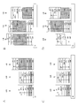
- FIG. 1 is a cross-sectional structure diagram of an EL display panel according to a first embodiment of the present invention. It is an equivalent circuit diagram of a block and a pixel of an EL display panel of the present invention. It is explanatory drawing of the manufacturing method of EL display panel of this invention. It is explanatory drawing of the vapor deposition apparatus and laser apparatus in manufacture of EL display panel of this invention. It is explanatory drawing of the laser apparatus in manufacture of the EL display panel of this invention. It is explanatory drawing of the laser apparatus in manufacture of the EL display panel of this invention. It is explanatory drawing of the manufacturing method of EL display panel of this invention. It is explanatory drawing of the manufacturing method of EL display panel of this invention. It is explanatory drawing of the manufacturing method of EL display panel of this invention.
- FIG. 47 is an explanatory diagram of a display device using an EL display panel of the present invention. It is sectional drawing of the conventional EL display panel. It is explanatory drawing of the manufacturing process of the conventional EL display panel.
- red pixels 37R, green pixels 37G, and blue pixels 37B are arranged in a matrix on a display screen 36.
- the EL display panel and EL display device of the present invention are not limited to those in which pixels are arranged in a matrix. If the display screen 36 has a plurality of color portions, it is within the technical scope of the present invention. For example, a display panel in which yellow pixels 37Y and blue pixels 37B are formed in a matrix may be used. Further, the display panel is not limited to a display panel in which pixels are arranged in a matrix, and may be an EL display panel that displays predetermined characters and shapes.
- Any EL display panel having a first color display portion and a second color first display portion may be used.
- the present invention modifies the light emitting layer material by irradiating a part of the display region with laser light or the like, an EL display panel having a region that emits light and a region that is modified and does not emit light is also used. This is a technical category of the invention.
- “reforming” means that the formed EL element 22 and a part of the light emitting layer 17 are irradiated with light, and the portion irradiated with the light is “modified”.
- the technical idea of the present invention can be applied.
- the present invention can also be applied to an EL display panel displaying a single color character.
- the light emitting layer 17 is formed by a process such as vapor deposition, and then the light emitting layer 17 is irradiated with a laser beam or the like to “modify” the light emitting layer 17.
- the present invention is not limited to this.
- the light emitting layer 17 may be “modified” by irradiating the light emitting layer 17 with laser light or the like while forming the EL element 22 and the light emitting layer 17 in a process such as vapor deposition.
- Irradiation of the laser light 59 to the light emitting layer 17 and the like is performed in a vacuum.
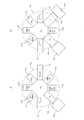
- FIG. 2 is a structural diagram of an EL display panel of the present invention and an equivalent circuit diagram of a pixel.
- red pixels 37R, green pixels 37G, and blue pixels 37B are arranged in a matrix.
- a pixel electrode 15R and a reflective film 12R are formed or arranged on the red pixel 37R
- a pixel electrode 15G and a reflective film 12G are formed or arranged on the green pixel 37G
- a pixel electrode 15B and a reflective film 12B are formed on the blue pixel 37B. Or have been placed.
- FIG. 2A is a structural diagram of the EL display panel of the present invention
- FIGS. 2B and 2C are equivalent circuit diagrams of the pixel 37.
- FIG. FIG. 2B is an equivalent circuit diagram in the case where the transistor 21 configuring the pixel 37 is configured by a P-channel transistor.
- FIG. 2C is an equivalent circuit diagram in the case where the transistor 21 configuring the pixel 37 is configured by an N-channel transistor.
- the pixel 37 may be configured using both an N-channel transistor and a P-channel transistor.
- TFTs 21a and 21b In the pixel 37, thin film transistors (TFTs) 21a and 21b, capacitors 23, and EL elements 22 are formed.
- the switching transistor 21a functions as a switching element that supplies the video signal output from the source driver circuit 32 to the gate terminal of the driving transistor 21b.
- the driving transistor 21 b functions as a driving transistor that supplies current to the EL element 22.
- the gate terminal of the switching transistor 21a of each pixel 37 is connected to the gate signal line 34, and the source terminal or drain terminal of the switching transistor 21a is connected to the source signal line 35 or the gate terminal of the driving transistor 21b. .
- the source terminal or drain terminal of the driving transistor 21 b is connected to the electrode to which the anode voltage Vdd is applied or the anode terminal of the EL element 22.
- the anode terminal of the EL element 22 is connected to the drain terminal or the source terminal of the driving transistor 21b, and the cathode terminal of the EL element 22 is connected to the cathode electrode 19 to which the cathode voltage Vss is applied.
- the driving transistor 21b and the switching transistor 21a are described as thin film transistors, but are not limited to thin film transistors, and may be transistors formed on a silicon wafer.
- the transistor 21 may be a FET, a MOS-FET, a MOS transistor, or a bipolar transistor.
- the anode electrode (pixel electrode) 15 constituting the EL element 22 is made of ITO which is a transparent electrode.
- a reflective film 12 is formed below the pixel electrode 15.
- the capacitor 23 may be formed using the reflective film 12 and the pixel electrode 15 as electrodes.
- the reflective film 12 does not need to be an electrode, and may be a film that reflects light.
- a reflective film made of a multilayer film is exemplified as a dichroic mirror.
- the storage capacitors C can be made different for the red, green, and blue pixels 37.
- the pixel electrode 15 is not limited to a transparent electrode, and may be formed of a metal material such as aluminum or silver. In this case, the pixel electrode 15 becomes a reflective film. Further, the reflective film 12 and the pixel electrode 15 may be laminated.
- the insulating film 14 is formed between the pixel electrode 15 and the reflective film 12, but the present invention is not limited to this. 14 may be any material as long as it has optical transparency as a function. For example, you may have electroconductivity.
- the pixel electrode 15R corresponds to the pixel 37R in FIG. 2, and similarly, the pixel electrode 15G corresponds to the pixel 37G, and the pixel electrode 15B corresponds to the pixel 37B.
- the technical idea of the manufacturing apparatus, the manufacturing method, the EL display panel, etc. of the present invention is that a bottom emission type EL element having no reflective film 12 and having a cathode 19 as a reflective film and taking out light only from the lower electrode side. 22 is also applicable.
- the TFT substrate 52 is a glass substrate on which the transistor 21, the pixel electrode 15 and the like are formed.
- a substrate made of resin may be used instead of the glass substrate.
- substrate formed with the polyimide resin may be sufficient.
- coated and hardened the varnish on the plane may be sufficient.
- substrate consisting of a metal material and a ceramic material may be sufficient.
- an example in which the light emitting layer 17 and the like are formed on the TFT substrate 52 will be described as an example.
- the present invention is not limited to an EL display panel using the TFT substrate 52.
- a simple matrix EL display panel in which TFTs are not formed or a character display EL display panel that displays fixed characters may be used.
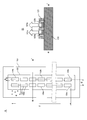
- FIG. 1 is a cross-sectional configuration diagram of an EL display panel of the present invention.
- a pixel 37 made of the transistor 21 or the like is formed on the TFT substrate 52, and a planarizing film 28 made of a photosensitive resin is provided thereon as an example.
- the reflective film 12 may be formed below the planarizing film 28 or may be formed above the planarizing film 28.
- a transparent conductive film made of ITO or IZO is formed on the planarization film 28, and the transparent conductive film is patterned to form a red pixel electrode 15R, a green pixel electrode 15G, and a blue pixel electrode 15B. .
- the pixel electrode 15 is electrically connected to one terminal of the driving transistor 21b through a contact hole (not shown) of the planarizing film 28.
- the insulating film 14 formed below each pixel electrode 15 has a film thickness for adjusting the optical distance L of the EL element.
- the present invention has a configuration in which the thickness of one of the insulating films 14 is different in the insulating film 14 below the pixel electrodes 15 of a plurality of colors.
- the optical distance (Optical Path Length) is also called an optical path length.
- the distance (physical distance) that light actually travels is multiplied by the refractive index.
- the refractive index of the substance of each layer which comprises the EL element of each color does not have a large difference, the optical distance L and the physical distance of the EL element of each color are relatively proportional. Therefore, the optical distance L may be replaced with a physical distance or read.
- a plurality of light-emitting layers are formed on at least one EL element, which is different from the light-emitting layer 17 of the other color EL element, and the optical distance L
- the optical distance L of at least one EL element is different from the optical distance L of the EL elements of other colors.
- the main wavelength ⁇ 1 nm of light emitted from the light emitting layer 17R is longer than the main wavelength ⁇ 2 nm of light emitted from the light emitting layer 17G (second light emitting layer).
- the main wavelength ⁇ 2 is longer than the main wavelength ⁇ 3 nm of light emitted from the light emitting layer 17B (third light emitting layer).
- the emission color of the light emitting layer 17R is red
- the emission color of the light emitting layer 17G is green
- the emission color of the light emitting layer 17B is blue.
- a light emitting layer 17R, a light emitting layer 17G, and a light emitting layer 17B are formed on the red pixel electrode 15R.
- a distance L1 between the reflective film 12R and the cathode electrode 19R is an optical distance of the red EL element 22.
- a light emitting layer 17G and a light emitting layer 17B are formed on the green pixel electrode 15G.
- a distance L2 between the reflective film 12G and the cathode electrode 19G is an optical distance of the green EL element 22.
- a light emitting layer 17G and a light emitting layer 17B are formed on the blue pixel electrode 15B.
- a distance L3 between the reflective film 12B and the cathode electrode 19 is an optical distance of the blue EL element 22.
- a light emitting layer 17R, a light emitting layer 17G, and a light emitting layer 17B are formed in common above the red pixel electrode 15R, the green pixel electrode 15G, and the blue pixel electrode 15B.
- the light emitting layer 17R is formed as a continuous film in common with a plurality of color pixels (a red pixel 37R, a green pixel 37G, and a blue pixel 37B).
- the light emitting layer 17G is formed as a common and continuous film for a plurality of color pixels
- the light emitting layer 17B is formed as a common and continuous film for a plurality of color pixels. .
- the light emitting layer 17R, the light emitting layer 17G, and the light emitting layer 17B are formed on the entire display screen 36 using a rough vapor deposition mask (not shown).
- the rough vapor deposition mask is a mask having an opening on the display screen 36 and not having an opening for each pixel.
- the red wavelength has the longest wavelength
- the blue wavelength has the shortest wavelength
- the green wavelength is intermediate between the red and blue wavelengths. Therefore, the optimum optical distance L for each color is red optical distance L1> green optical distance L2> blue optical distance L3.
- the interference orders are the same order for red, green and blue.
- a transparent metal film (MgAg19) is formed on the light extraction side electrode, and a reflection film 12 is formed on the opposite side to the light extraction side.
- Silver (Ag) which is a highly reflective metal, is used as the reflective film.
- the interference order m 0 or 1 is selected.
- the film thickness constituting the EL element is thin, and the amount of organic material to be used can be reduced, so that the cost can be reduced.
- the color change due to the viewing angle direction hardly occurs.
- a hole transport layer 16 is formed on the pixel electrode 15.
- a hole injection layer (HIL: Hole injection layer, not shown) may be formed between the pixel electrode 15 and the hole transport layer 16.
- the film thickness of the hole transport layer 16 of the pixel electrode 15 may be different for the red, green, and blue pixels 37.
- the hole transport layer 16R is formed on the pixel electrode 15R
- the hole transport layer 16G is formed on the pixel electrode 15G
- the hole transport layer 16B is formed on the pixel electrode 15B
- each hole transport layer is formed.
- the film thickness of 16 is varied.
- a red light emitting layer 17R, a green light emitting layer 17G, and a blue light emitting layer 17B are formed above the pixel electrode 15. ing.
- the light emitting layer 17R and the light emitting layer 17G are different in at least one of the host material and the guest material and have different emission colors.
- the absorption spectrum of the guest material contained in the light emitting layer 17R at least partially overlaps the light emission spectrum of the light emitting layer 17G.
- the absorption spectrum of the guest material contained in the light emitting layer 17G at least partially overlaps the light emission spectrum of the light emitting layer 17B.
- the light emitting layer 17R above the pixel electrode 15G and the pixel electrode 15B is modified.
- the light emitting layer 17G above the pixel electrode 15B is also modified.
- the light emitting layer 17R above the pixel electrode 15R in FIG. 1 emits red light.
- the light emitting layer 17R above the pixel electrode 15G and the pixel electrode 15B does not emit light.
- the light emitting layer 17G above the pixel electrode 15G emits green light.
- the light emitting layer 17G above the pixel electrode 15B does not emit light.
- the light emitting layer 17R above the pixel electrode 15R in FIG. 1 contains a guest material that emits light at a higher concentration than the light emitting layer 17R above the pixel electrode 15G and the pixel electrode 15B. Most of the guest material included in the light emitting layer 17R above the pixel electrode 15R in FIG. 1 can emit light, and most of the guest material included in the light emitting layer 17R above the pixel electrode 15G and the pixel electrode 15B is quenched. Or not excited. Alternatively, the light emitting layer 17R above the pixel electrode 15R has at least one of hole mobility and hole injection efficiency smaller than the light emitting layer 17R above the pixel electrode 15G and the pixel electrode 15B.
- the light emitting layer 17G above the pixel electrode 15R and the pixel electrode 15G contains a guest material that emits light at a higher concentration than the light emitting layer 17G above the pixel electrode 15B. Most of the guest material of the light emitting layer 17G above the pixel electrode 15B is quenched or not excited. Alternatively, the light emitting layer 17G above the pixel electrode 15R and the pixel electrode 15G has an electrical characteristic different from that of the light emitting layer 17G above the pixel electrode 15B.
- the light emitting layer 17G above the pixel electrode 15R and the pixel electrode 15G has at least one of hole mobility and hole injection efficiency smaller than the light emitting layer 17G above the pixel electrode 15B.
- Most of the guest material included in the light emitting layer 17G above the pixel electrode 15R and the pixel electrode 15G can emit light, and most of the guest material of the light emitting layer 17G included in the light emitting layer 17G above the pixel electrode 15B is quenched. Or not excited.
- the light emitting layer 17R above the pixel electrode 15G and the pixel electrode 15B has at least one of the hole mobility and the hole injection efficiency of the light emitting layer 17R larger than the light emitting layer 17R above the pixel electrode 15R. .
- the light emitting layer 17G above the pixel electrode 15B is larger in at least one of the hole mobility and the hole injection efficiency of the light emitting layer 17G than the pixel electrode 15R and the light emitting layer 17G above the pixel electrode 15G. .
- an EL display panel having an EL element 22 having a structure in which a hole transport layer 16, a light emitting layer 17, and an electron transport layer 18 are formed above a pixel electrode 15 and a cathode electrode 19 as a common electrode is formed.
- An EL display panel having an EL element 22 having a reverse structure in which an electron transport layer 18, a light emitting layer 17, and a hole transport layer 16 are formed above the pixel electrode 15 and a cathode electrode 19 as a common electrode is formed may be used.
- the EL element 22 having an inverted structure it is necessary to replace the hole transport layer with an electron transport layer in the drawings of the present invention, the present specification, and the description thereof. In addition, it is necessary to replace the hole injection layer with an electron injection layer.
- the light emitting layer 17R above the pixel electrode 15G and the pixel electrode 15B is irradiated with laser light 59 in the ultraviolet light region, the violet light region, or the blue light region by the manufacturing method of the present invention.
- the laser light 59 is mainly absorbed by the guest material of the light emitting layer 17R.
- UV light is electromagnetic waves of invisible light having a wavelength of 10 nm to 400 nm, that is, shorter than visible light and longer than soft X-rays.
- Infrared rays are electromagnetic waves that have a longer wavelength (lower frequency) than visible red light and a shorter wavelength than radio waves.
- the covalent bond chain is broken by the absorption of the laser beam 59.
- the radical of the covalent bond chain generates a double bond.
- the atoms of other covalent bond chains are extracted and bonded.
- a cross-linked structure is generated with another covalent bond chain, resulting in a change in the structure.
- the laser light 59 has narrow directivity and good straightness. For this reason, the light emitting layer 17 of the predetermined pixel 37 can be selected and irradiated with the laser light 59.
- the light emitting layer 17 of the predetermined pixel 37 can be selected and irradiated with the laser light 59.
- pixels 37 of the same color are arranged in the vertical direction (from the top to the bottom of the screen) as shown in FIG.
- the material of the light emitting layer 17 is also deposited between the adjacent pixel electrodes 15, but a source signal line 35 and the like are formed between the adjacent pixel electrodes 15.
- there is a predetermined interval between adjacent pixels 37 Therefore, even if the size of the laser spot 91 of the laser beam 59 is large, the light emitting layer 17 of the pixel adjacent in the lateral direction is not irradiated.
- the scanning direction of the laser light 59 can be controlled with high speed and accuracy by controlling the galvanometer mirror 62. Further, since the laser device 58 is disposed outside the vapor deposition chamber 56, maintenance is easy. The laser light 59 is generated outside the vapor deposition chamber 56, and the generated laser light 59 is guided into the vacuum inside the vapor deposition chamber 56 through the laser window 63. Therefore, the vacuum state in the vapor deposition chamber 56 can be maintained satisfactorily. Note that the laser device 58 may be disposed in the vapor deposition chamber 56. If the wavelength of the irradiated light is short, the light absorption rate to the material increases.
- the laser beam 59 having a short wavelength can narrow the spot diameter to near the diffraction limit, it is possible to reduce the thermal influence on the surroundings when processed, suitable for fine processing, and processing an ultra-high-definition EL display panel. be able to.
- the light emitting layer 17 and the like can be modified well in accordance with the shape of the pixel electrode 15.
- the laser device 58 is preferably a continuous oscillation mode device.
- the pulse oscillation type laser device 58 has strong laser light pulse energy.
- pixels that irradiate laser light 59 are discretely arranged like an EL display panel in which pixels are arranged in a matrix, it is preferable to use a pulse oscillation type laser device 58. Since the laser beam 59 output from the pulse oscillation type laser device 58 is on / off controlled by a Q switch, variations in pulse intensity are likely to occur. Therefore, it is desirable to modify the light emitting layer 17 and the like by irradiating a portion to be modified with a plurality of laser pulses.
- the laser pulse irradiation interval is preferably 50 nsec or more and 5 ⁇ sec or less.
- the irradiation interval of the laser pulse is such that the first laser pulse makes the light emitting layer 17 in a semi-dissolved state, and the next laser pulse is irradiated with the laser pulse before the light emitting layer 17 becomes a solid state.
- the same spot is irradiated multiple times with laser light.
- the energy of the laser beam applied to the same location is averaged, and the modified state becomes uniform.
- the irradiation interval of the laser light 59 is preferably 50 nsec or more and 5 ⁇ sec or less.
- the irradiation interval of the laser beam 59 is set so that the light emitting layer 17 is in a semi-dissolved state by the first laser beam 59 irradiation, and the next laser beam 59 is irradiated before the light emitting layer 17 is in a solid state. It is preferable to do.
- a laser device of a laser lift-off (LLO) device commercialized by Optopia Corporation can be used.
- the laser wavelength of the laser device of the laser lift-off device is 343 nm, and the line beam length is 750 mm.
- the line width is 30 ⁇ m, the energy density is 250 mJ / cm 2 , and the pulse width is 15 ns. Therefore, even in a large EL display panel, it is possible to irradiate laser light 59 to one pixel column with one laser spot 91 on one pixel column (from the upper end to the lower end of the screen).
- the appropriate pulse width of the laser beam 59 is not less than 10 nsec and not more than 80 nsec.
- examples of the laser device 58 include those using a solid-state laser having a wavelength of 355 nm and those using an excimer laser having 308 nm.
- the pixel 37 can be selected with high accuracy and the predetermined light emitting layer 17 can be modified.
- the laser light 59 has a high light intensity per unit area. Therefore, the light emitting layer 17 and the like can be modified in a short time.
- the fine vapor deposition mask 251 is not used unlike the conventional manufacturing method. Therefore, there is no problem of color mixture of emitted colors due to the positional deviation of the fine vapor deposition mask 251. Moreover, the cost of a vapor deposition manufacturing apparatus can be reduced. Since the fine vapor deposition mask 251 is not used, positioning of the fine vapor deposition mask 251 is not necessary, so that the manufacturing tact can be shortened.
- the combination of the guest material and the host material of the light emitting layer 17 is changed by the irradiation of the laser beam 59.
- the laser light 59 preferably uses light having a wavelength in the ultraviolet region.
- the manufacturing method / manufacturing apparatus of the present invention irradiates the film layer constituting the EL element 22, the light emitting layer 17, etc. with a laser beam or the like to modify it.
- the EL element 22 and the light emitting layer 17 irradiated with the laser light 59 are quenched, do not emit light, or hardly emit light.
- the pixel 37R recombination of electrons and holes is mainly generated in the light emitting layer 17R.
- the pixel 37G recombination of electrons and holes occurs mainly in the light emitting layer 17G.
- the pixel 37B it is generated mainly in the light emitting layer 17B.
- the pixel 37R recombination of electrons and holes mainly occurs in the light emitting layer 17R, but recombination may also occur in the light emitting layers 17G and 17B.
- each of the light emitting layers 17R, 17G, and 17B may emit light.
- the guest material included in the light emitting layer 17R absorbs energy excited by the light emitting layer 17G and the light emitting layer 17B and emits light.
- the guest material contained in the light emitting layer 17G is excited by absorbing light emitted from the light emitting layer 17B, but hardly absorbs light excited by the light emitting layer 17R. Further, the guest material included in the light emitting layer 17B hardly emits light by absorbing energy excited by the light emitting layer 17R or 17G.
- the emission color of the pixel 37R is substantially equal to the emission color of the light emitting layer 17R, and the pixel 37R emits red light.
- the pixel 37G recombination of electrons and holes mainly occurs in the light emitting layer 17G, but recombination may also occur in the light emitting layers 17R and 17B.
- the light emitting layer 17R above the pixel electrode 15G does not contain a guest material that emits light when irradiated with the laser light 59. Since the light emitting layer 17R of the pixel 37G does not contain a guest material that emits light, color conversion does not occur in the light emitting layer 17R. In the light emitting layer 17B, the above color conversion occurs. Therefore, the emission color of the pixel electrode 15G is substantially equal to the emission color of the light emitting layer 17G, and the pixel electrode 15G emits green light.
- the pixel 37B recombination of electrons and holes mainly occurs in the light emitting layer 17B, but recombination may also occur in the light emitting layers 17R and 17G.
- the light emitting layers 17R and 17G above the pixel electrode 15B do not contain a guest material that emits light when irradiated with the laser light 59, only the light emitting layer 17B emits light. Since the light emitting layer 17R and the light emitting layer 17G of the pixel 37B do not contain a guest material that emits light, color conversion does not occur in the light emitting layers 17R and 17G. Therefore, the emission color of the pixel 37B is substantially equal to the emission color of the light emitting layer 17B, and the pixel electrode 15B emits blue light.
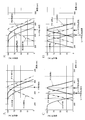
- the host material is difficult to absorb the laser light 59, and the guest material is a material that easily absorbs the laser light 59.
- the wavelength of the laser light 59 is selected such that the host material is less likely to be absorbed and the guest (dopant) material is more likely to be absorbed.
- the host material and guest material are selected such that when the guest material absorption rate is 75% or more, the host material absorption rate is 25% or less.
- the light absorptance (%) of the guest material and the host material is normalized and illustrated with the maximum light absorptance being 100%.
- guest material A is an example of a material having a characteristic of increasing the absorption rate (%) at a wavelength of 400 nm or less and having an absorption rate of 75% or more at the wavelength of laser light 59.
- the guest material B is an example of a material having a good absorption rate near the wavelength of the laser light 59.
- the wavelength of the laser light and the guest material so that the light absorption rate of the guest material and the light absorption rate of the host material are 3 times or more, preferably 4 times or more, at the wavelength of the laser light 59.
- the hole transport layer 16 has an absorptance of the laser beam 59 of the host material when the absorptivity of the laser beam 59 of the guest material is 75% or more, like the host material. It is preferable to select the hole transport layer 16 material that has a relationship of 25% or less.
- the present invention is not limited to the configuration in which the light emitting layer 17 is formed from a guest material and a host material.
- the light emitting layer 17 may be formed of a single material.
- the single material is modified.
- the technical idea of the present invention is to irradiate the organic film forming the EL element 22 with laser light 59 or the like to modify the light emitting layer 17 or the like. In this case, the relationship between the light-emitting layer 17 and the absorption rate of the laser light 59 of the hole transport layer material is required. That is, as shown in FIG.
- the wavelength of the laser light 59 needs to have a relationship between the light absorption rate (%) of the hole transport layer and the light absorption rate (%) of the light emitting layer 17. Therefore, as shown in FIG. 3B, when the absorption rate of the laser beam 59 of the material of the light emitting layer 17 is 75% or more, the absorption rate of the laser beam 59 of the hole transport layer material is 25% or less. It is preferable to select an appropriate hole transport layer material.
- the light emitting layer material A is an example of a material having a characteristic of increasing the absorption rate (%) at a wavelength of 400 nm or less and having an absorption rate of 75% or more at the wavelength of the laser beam 59.
- the light emitting layer material B is an example of a material having a good absorption rate near the wavelength of the laser light 59.
- the hole transport layer material has a light absorption rate of 25% or less at the wavelength of the laser beam 59.
- the rate difference Preferably, the difference in light absorption rate is 4 times or more.
- the red light emitting layer 17R emits red light in the light emitting layer above the pixel electrode 15R.
- the green light emitting layer 17G and the blue light emitting layer 17B do not emit light.
- the red light emitting layer 17R is “light emitting”, the green light emitting layer 17G is “quenched”, and the blue light emitting layer 17B is “quenched”.
- the green light emitting layer 17G emits green light.
- the red light emitting layer 17R and the blue light emitting layer 17B do not emit light.
- the red light-emitting layer 17R is “quenched”, the green light-emitting layer 17G is “light-emitting”, and the blue light-emitting layer 17B is “quenched”.
- the blue light emitting layer 17B emits blue light.
- the red light emitting layer 17R and the blue light emitting layer 17B do not emit light.
- the red light-emitting layer 17R is “quenched”, the green light-emitting layer 17G is “quenched”, and the blue light-emitting layer 17B is “light-emitting”.
- the hole transport layer 16 functions to transport holes to the light emitting layer 17 and is in contact with the light emitting layer so that excitation energy does not move from the light emitting layer 17 and further interacts with other layers to form an exciplex. Therefore, a material having an energy band gap larger than that of the light emitting layer 17 is used.
- a material having an energy band gap larger than that of the light emitting layer 17 is used.
- TPD, ⁇ -NPD, NBP, and TCTA are exemplified.
- the hole injection layer has a HOMO level between the HOMO level of the hole transport layer 16 and the work function of the anode, and functions to lower an injection barrier dug from the anode to the organic layer.
- An electron transport layer 18 is formed above the light emitting layer 17.
- An electron injection layer (EIL: Electron injection layer not shown) may be formed between the electron transport layer 18 and the cathode electrode 19.
- the type of the electron transport layer 18 may be different for the red pixel 37R, the green pixel 37G, and the blue pixel 37B.
- the electron transport layer 18 has a function of injecting and transporting electrons from the cathode electrode (cathode) 19.
- a material having a wide band gap is preferable. Examples of the material for the electron transport layer 18 include tris (8-hydroxyquinolinato) aluminium (Alq3), or derivatives or metal complexes thereof.
- the light emitting layer 17 is a region where holes injected from the anode side and electrons injected from the cathode side are recombined when a voltage is applied to the pixel electrode (anode) 15 and the cathode electrode (cathode) 19.
- the light emitting layer may be composed of one layer composed of one or more of these light emitting materials, or a layer in which a light emitting layer composed of a compound different from the light emitting layer is laminated. It may be.
- the EL element 22 has a resonator structure, multiple interference is caused between the light reflecting surface of the cathode 19 and the light reflecting surface of the reflecting film 12 which are configured to be semi-transmissive and semi-reflective.
- the optical distance L between the light reflecting surface of the reflecting film 12 and the light reflecting surface on the cathode 19 side is defined by the wavelength of light to be extracted, and the film thickness and interference conditions of each layer so as to satisfy this optical distance L. Is set.
- the insulating film 14 of the red pixel 37R, the green pixel 37G, and the blue pixel 37B is adjusted, and the optical distance L between the red pixel 37R, the green pixel 37G, and the blue pixel 37B is adjusted. It was formed so as to maximize the cavity effect.
- the present invention is not limited to this.
- FIG. 28A shows an embodiment in which the interference order of red (R) pixels and green (G) pixels is 0th order, and the interference order of blue (B) pixels is 1st order.
- the insulating film 14 is formed with different thicknesses for red (R) pixels and green (G) pixels.
- the hole transport layer (HTL) of the blue (B) pixel is formed thick.
- the hole transport layer is not formed by one deposition but formed by a plurality of depositions. Moreover, you may form the hole transport layer formed by multiple times of vapor deposition with the material of a different hole transport layer.
- the optical distance L that exhibits the cavity effect is proportional to the emission wavelength.
- the red wavelength is longer than the green wavelength
- the green wavelength is longer than the blue wavelength.
- the red optical distance L1 is longer than the green optical distance L2, and the green optical distance L2 is longer than the blue optical distance L3.
- the film thickness of the EL element 22 is about 100 nm.
- the film thickness of the blue pixel 37B is the thinnest. If the optical distance L is thin, defects due to dust during manufacturing tend to occur. Therefore, more defects are generated in the blue pixel 37B than in the red pixel 37R, and the yield of the EL display panel is lowered due to the defect in the blue pixel 37B.
- the yield of the EL display panel can be improved by setting the interference order of the blue pixel 37B to be the first order and making the film thickness of the EL element 22 larger than that of the other color pixels.
- the red (R) pixel, the green (G) pixel, and the blue (B) pixel can realize the optimum optical distance L corresponding to the emission wavelength, thereby exhibiting the cavity effect and good color reproducibility. Can be realized.
- the interference order of the blue (B) pixel among the three colors is set to the first order, but the present invention is not limited to this, and as shown in FIG.
- the red (R) pixel, All the interference orders of the green (G) pixel and the blue (B) pixel may be primary.
- the configuration in which the film thicknesses of the red (R) pixel, the green (G) pixel, and the blue (B) pixel are not limited is not limited to the common film layer.
- the transport layer (HTL), the green (G) pixel may be the light emitting layer (EML), and the blue (B) pixel may be the insulating film 14B.
- the interference order may be the same for the red (R) pixel, the green (G) pixel, and the blue (B) pixel, and the optical distance L may be adjusted with a common film layer.
- the interference order of the red (R) pixel, the green (G) pixel, and the blue (B) pixel is made common with the 0th order, and the red (R) pixel, the green (G) pixel, and the blue (B) pixel are insulated. This is an example in which an optimum cavity effect is realized by using different films and good color reproducibility is realized.
- the blue (B) pixel may not have an insulating film.
- the reflective film 12B and the pixel electrode 15B are stacked.
- the interference order may be different for the red (R) pixel, the green (G) pixel, and the blue (B) pixel, and the interference order may be the primary for a plurality of colors.
- the red (R) pixel has an interference order of 0th order
- the green (G) pixel and blue (B) pixel has an interference order of 1st order.
- the light emitting layer 17G is formed thick
- the blue (B) pixel the insulating film 14B is formed thick.
- a bank (bank) 95 is formed around the pixel electrode 15.
- the bank 95 mainly prevents the fine vapor deposition mask 251 from coming into contact with the pixel electrode 15 and the like when the fine vapor deposition mask 251 is disposed, and prevents the light emitting layer 17 from being mixed between adjacent pixels. Formed as a purpose.
- the fine vapor deposition mask 251 when the fine vapor deposition mask 251 is not used, when the light emitting layer 17 is modified by irradiating narrow directivity light such as the laser light 59, or when no color mixture occurs between the pixels, Needless to say, the bank 95 does not need to be formed as shown in FIGS. 26 and 27, for example, when color mixing between pixels can be prevented or suppressed.
- the manufacturing apparatus, manufacturing method, EL display panel, and the like of the present invention exemplify a top emission type EL panel that forms the reflective film 12 and extracts light generated in the light emitting layer 17 from the transparent cathode electrode 19 side. I will explain. However, the present invention is not limited to this, and can be applied to a bottom emission type EL display panel in which the cathode 19 is used as a reflection film so that light is extracted only from the lower electrode side.
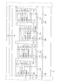
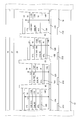
- FIG. 4 is a configuration diagram and an explanatory diagram of a vapor deposition apparatus of an EL display panel manufacturing apparatus according to the present invention.
- the EL display panel deposition apparatus of the present invention includes a deposition chamber 56 having a metal evaporation source 65 and an organic evaporation source 66.
- the vapor deposition chamber 56 includes a moving stage 51 for holding the TFT substrate 52, a temperature adjusting plate 53 for holding or adjusting the TFT substrate 52 at a predetermined temperature, a vacuum pump (vacuum exhaust device) 54, a vacuum pump 54, and a vapor deposition chamber.
- An exhaust duct 55 that connects to 56 is provided.
- the vacuum degree of the vapor deposition chamber 56, the transfer device chamber 117, and the laser device chamber 118 of the film forming apparatus 116 is preferably maintained at a vacuum degree of 1 ⁇ 10 ⁇ 3 Pa or more. More preferably, the degree of vacuum is 1 ⁇ 10 ⁇ 4 Pa or more.
- a plurality of vapor deposition power supplies and film thickness meters are installed for the host material and guest material so that two kinds of organic materials can be formed by the co-evaporation method.
- the intensity of the laser beam 59 generated by the laser device 58 is adjusted by the light amount adjustment filter 60.
- the laser light 59 for modifying the light emitting layer 17 is mainly a laser light 59 in the ultraviolet wavelength region. The matters relating to the laser device 58 described with reference to FIG. 4 and the like can be applied to the deposit 201 removal device or the deposit 201 reforming device illustrated in FIG.
- the transmittance (reflectance) is changed by rotating the ⁇ / 2 wavelength plate in front of the polarizing beam splitter.
- the laser beam 59 generated by the laser device 58 is shaped into a rectangle or an ellipse by the cylindrical lens 61 as necessary. Further, it is shaped into a substantially rectangular or circular shape so as to substantially match the pixel shape with a slit mask.
- the laser light 59 whose intensity has been adjusted by the light amount adjustment filter 60 enters the galvanometer mirror 62.
- the galvanometer mirror 62 scans the laser beam 59 in the XY two-dimensional area (TFT substrate 52 or donor film 197).
- the galvanometer mirror 62 uses two motors (rotary encoders) that scan the laser beam 59 in the X and Y axis directions.
- the laser beam 59 enters the vapor deposition chamber 56 through a laser window 63 disposed in the vapor deposition chamber 56.
- the laser beam 59 is applied to the TFT substrate 52 in a high vacuum state.
- the laser window 63 is made of quartz glass.
- the laser device 58 is disposed in the atmosphere outside the vapor deposition chamber 56, and a laser beam 59 is incident from the laser window 63 into the vacuum of the vapor deposition chamber 56. Therefore, the operation and maintenance of the laser device 58 are easy.
- an f ⁇ (F-theta) lens 64 is provided as a lens for forming an image of the laser beam 59 on the TFT substrate 52.
- the f ⁇ lens 64 is designed so that the scanning speed is constant at the lens peripheral part and the central part by changing the curvature of the lens surface of the lens.
- the laser light 59 generated by the laser device 58 is changed in the direction of the laser light by the galvanometer mirror 62 and is irradiated on the surface of the TFT substrate 52 or the donor film 197 by the f ⁇ lens 64.
- the position of the f ⁇ lens 64 is changed between the f ⁇ lens 64a and the f ⁇ lens 64b as necessary.
- the focus position of the laser light 59 can be changed.
- the position of the moving stage 51 is changed from the moving stage 51a to the moving stage 51b.
- the focus position of the laser beam 59 can be changed.
- the focus position is changed, the irradiation range of the laser beam 59 and the size of the laser spot 91 can be changed.
- FIG. 5 and 6 are explanatory diagrams for explaining a method for modifying the light emitting layer 17 and the like by the laser device 58.
- the apparatus for performing the modification includes a light detection device 77 and a light control device 78.
- the laser device 58 generates laser light 59.
- the laser beam 59 is incident on the light separation mirror 72b.
- the light separation mirror 72b has a half mirror function in order to monitor the intensity of the laser light 59 generated by the laser device 58.
- the light separation mirror 72 b reflects a predetermined proportion of the laser light 59.
- the laser beam 59b reflected by the light separation mirror 72b is reflected by the mirror 73b, is condensed by the lens 74c, and enters the optical amplifier circuit 76b.
- FIG. 6B is a circuit diagram of the optical amplifier circuit 76.
- the optical amplifier circuit 76 includes a photodiode (PD), an operational amplifier 81, a resistor R, a capacitor C, and the like.
- the optical amplifying circuit 76 is a photodiode (PD) and photoelectrically converts the laser light 59b.
- the laser light subjected to the photoelectric conversion is amplified and becomes an analog signal voltage V2.
- the analog signal voltage V2 is converted into a digital signal by the A / D conversion circuit 80b and input to the laser control circuit 79.
- the laser control circuit 79 detects the intensity of the laser light 59 and feedback-controls the laser device 58 so as to be within a predetermined intensity value or intensity range. By the feedback control, the intensity of the laser beam 59 is set within a predetermined value range.
- Laser light 59a from the laser device 58 passes through the light separation mirror 72b and the light separation mirror 72a, is guided from the laser window 63 of the vapor deposition chamber 56 to the vapor deposition chamber 56, and enters the light emitting layer 17 to be modified.
- the light separation mirror 72a functions as a wavelength separation mirror.
- An optical multilayer film is formed on the surface of the light separation mirror 72a, and has a function of transmitting a wavelength in a specific band and reflecting a wavelength in a specific band.
- the light separation mirror 72 a transmits the laser light 59 a and reflects the light 71 having the fluorescence / phosphorescence wavelength excited by the light emitting layer 17.
- Light 71 having a fluorescent / phosphorescent wavelength is collected by a lens 74a, bent in a direction by a mirror 73a, and collected by a lens 74b.
- the optical filter 75 transmits only wavelengths within a certain range of the collected light 71.
- the optical filter 75 is excited and used to detect the generated light intensity of a wavelength within a predetermined band range.
- the optical amplifier circuit 76a is a photodiode (PD) and photoelectrically converts the light 71.
- the light-electrically converted light 71 is amplified and becomes an analog signal voltage V1.
- the analog signal voltage V1 is converted into a digital signal by the A / D conversion circuit 80a and input to the laser control circuit 79.
- the laser control circuit 79 detects the intensity of the light 71 having the fluorescence or phosphorescence wavelength, detects whether it is within a predetermined intensity value or intensity range.
- the irradiation position of the laser beam 59a is changed or moved. Further, the intensity of the laser beam 59a is changed.
- the light emitting layer 17 on which the laser light 59a is deposited is irradiated, and the light emitting layer 17 is excited to emit fluorescence / phosphorescence 71.
- the laser light 59a modifies the irradiated light emitting layer 17.
- the intensity of the fluorescence / phosphorescence 71 generated by the light emitting layer 17 decreases. Therefore, the laser beam 59 a has both a function of exciting the light emitting layer 17 and a function of modifying the light emitting layer 17. In particular, since the laser beam 59a is light in the ultraviolet region, the light emitting layer 17 is easily excited.
- the light detection device 77 includes an optical filter 75 for separating the fluorescence / phosphorescence 71 and a light separation mirror 72a, so that detection is easy.
- the transmission wavelength of the optical filter 75 is switched according to the wavelength of the fluorescence / phosphorescence 71 generated by the light emitting layer 17. This is because the amplification factor of the optical amplifier circuit 76a differs depending on the wavelength and intensity of the fluorescence / phosphorescence 71 emitted from the light emitting layer 17.
- the wavelength / intensity of the fluorescent / phosphorescent light 71 emitted from the light emitting layer and the light emitting layer 17R, the wavelength / intensity of the fluorescent / phosphorescent light 71 emitted from the light emitting layer 17G, and the wavelength / intensity of the fluorescent / phosphorescent light 71 emitted from the light emitting layer 17B. Are different from each other, so that the optimum value is controlled in accordance with the fluorescence / phosphorescence 71 of each light emitting layer 17.
- the modified state of the light emitting layer 17 can be grasped.
- the reformed state exceeds a predetermined set value, it is determined that the modification of the pixel 37 to be irradiated with the laser beam 59a is completed, and the laser beam 59a is positioned to the next pixel to be modified.
- the light detection device 77 and the light control device 78 are attached to the same member. Therefore, as the irradiation position of the laser beam 59 moves, the light detection device 77 also moves at the same time. Needless to say, the light detection device 77 may be installed inside the vapor deposition chamber 56 and the light control device 78 may be installed outside the vapor deposition chamber 56.
- the optical amplifier circuit 76 may be disposed on the back surface of the TFT substrate 52.
- the laser light 59c is detected by an optical amplifier circuit 76c disposed on the back surface of the TFT substrate 52.
- the fluorescence / phosphorescence 71 a is detected by an optical amplifier circuit 76 c disposed on the back surface of the TFT substrate 52.
- the photodetection device 77 is configured so that the angle ⁇ of the lens 74 that detects the fluorescence / phosphorescence 71 can be varied, as shown in FIG. 6C.
- the angle ⁇ is changed by a control device installed outside the vapor deposition chamber 56.
- the angle ⁇ is automatically adjusted to an angle at which the fluorescence / phosphorescence 71 can be detected most strongly.
- the positions of the lenses 74a to 74b and the light detection devices 77a to 77b are changed or set so that the intensity of the fluorescence / phosphorescence 71 can be detected most strongly.
- the light detection device 77 is preferably configured so that not only the intensity of the fluorescence / phosphorescence 71 but also the wavelength can be discriminated.
- the ratio or amount of change of the red emission wavelength to the green emission wavelength is detected. If the light emission wavelength changes to green, the red light emission wavelength eventually becomes a “quenched” state, and it can be detected that no light is emitted.
- light for exciting the light emitting layer 17 may be separately generated and the light emitted to the light emitting layer 17G.
- a configuration in which a generator for the laser light 59 for fluorescence / phosphorescence emission is separately installed and the light emitting layer 17 to be modified is irradiated with the laser light 59 is exemplified.
- the light emitting layer 17 When the intensity of the generated fluorescence / phosphorescence 71 becomes a predetermined value or less, the light emitting layer 17 is in a quenching state. When the light is extinguished, it is determined that the modification of the light emitting layer 17G is completed, and the irradiation position of the laser light 59a is moved to the next pixel. Further, the time required for the modification is measured, and the intensity of the laser beam 59a is controlled. By monitoring the intensity / wavelength of the fluorescence / phosphorescence 71 with the photodetection device 77, the light emitting layer 17 of the pixel to be modified can be accurately extinguished.
- the intensity of the laser light applied to the light emitting layer 17 can be set to a stable and constant value.
- the light emitting layer 17 of the pixel can be accurately extinguished.
- the laser device 58 has a function of generating light having a wavelength of 310 nm to 400 nm in the vicinity of A ultraviolet (UV-A) and irradiating the generated pixel electrode 15 with the generated light. Since a laser device that generates ultraviolet rays has a large energy of photons, it can perform photolytic processing that directly dissociates molecular bonds when irradiated with materials (mainly organic substances) having weakly bonded portions. In photolytic processing, the energy that hits the work is not heated but mainly used for disassembling, so the processed surface becomes extremely sharp. Examples of laser devices that generate light having a wavelength in the ultraviolet region include ultraviolet lasers (third and fourth harmonics of YAG lasers), solid ultraviolet lasers, and excimer lasers.
- the organic material or the like at the processing position can be easily modified or evaporated. Since the organic material is evaporated in a vacuum, the organic material is not carbonized and does not affect the peripheral portion of the position irradiated with the laser light.
- the laser beam 59 is preferably configured so that it can be irradiated from above the TFT substrate 52. Even when the guest material is heated by the laser beam 59 and the heated guest material is sublimated, adhesion to the peripheral portion can be suppressed.
- the laser device 58 may be a femtosecond laser device.
- the femtosecond laser device is a pulse laser, and its pulse width is a femtosecond level laser device.
- the femtosecond laser device is characterized by non-thermal processing, unlike a CO 2 laser device and a YAG laser device used for normal processing. When a CO 2 laser beam or YAG laser beam is applied to an object to be processed, the molecules absorb the light energy, vibrate, are converted into thermal energy, and are processed by melting and evaporating.
- processing can be performed by a phenomenon called “ablation” in which molecular bonds are cut by light energy and molecules are removed without thermal diffusion to the peripheral portion. Therefore, only the portion irradiated with the laser beam 59 is modified and the peripheral portion is not thermally affected.
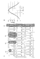
- the size of the laser spot of the laser beam 59 may be smaller than the pixel electrode 15 as illustrated in the laser spot 91a in FIG. This is because the entire region of the pixel electrode 15 can be irradiated with the laser beam 59a by moving the laser spot 91a within the pixel electrode 15.
- the intensity distribution of the laser beam 59a is a Gaussian distribution.
- the range W1 of the intensity 63% of the Gaussian distribution of the laser beam 59a be the width of the light emitting layer 17 to be modified.
- the width W2 of the intensity 80% of the Gaussian distribution of the laser light 59a is set to the width of the light emitting layer 17 to be modified.
- the guest material of the light emitting layer 17 is modified or evaporated is generated by the laser device 58 and can be easily realized by controlling the intensity of the laser light 59 applied to the TFT substrate 52.
- the intensity of the laser beam 59a is changed by the light quantity adjustment filter 60.
- the light amount adjustment filter 60 is preferably configured so that the intensity of the laser beam 59a can be changed in units of pulses of the laser beam 59a.
- the laser spot 91b has a shape that irradiates one pixel electrode 15 over the entire range.
- the laser spot 91c has a shape in which a plurality of pixel electrodes 15 are irradiated simultaneously.
- a stripe-shaped laser spot may be used, and the TFT substrate 52 may be irradiated with a line-shaped laser beam 59.
- the laser spot 91 of the laser light 59 is applied to the pixel 37 to be modified, and the position of the laser spot 91 is moved to modify the guest material or the host material of the light emitting layer of the pixel 37.
- the host material and guest material for forming the light emitting layer 17 are evaporated.
- the adjacent column of pixels 37 may be irradiated with the laser beam.
- a slit mask 92 is used so that the adjacent pixel columns are not irradiated with the laser light 59.
- the laser spot 59 is irradiated from the slit of the slit mask 92 to the light emitting layer 17 in the laser spot 91a.
- the laser spot 91a is scanned in the a direction, and the pixels in the pixel column direction are sequentially modified.
- the laser spot 91b is irradiated with the laser light 59 from the slit of the slit mask 92.
- the laser spot 91a is scanned in the b direction, and the pixels in the pixel column direction are sequentially modified.
- the laser beam 59 is irradiated to the light emitting layer 17 from the slit of the slit mask 92 in the rectangular laser spot 91c.
- the rectangular laser spot 91c illuminates one pixel row of the display screen 36 at the same time.
- the light emitting layer 17 of the pixel example irradiated with the laser light 59 the light emitting layer 17 in one pixel column is simultaneously modified.
- the slit mask 92 moves in accordance with the movement of the laser spot 91 and modifies the light emitting layer 17 of a pixel of a predetermined color on the display screen 36.
- the laser spot 91 moves according to the hole position of the slit mask, and modifies the light emitting layer 17 of a pixel of a predetermined color on the display screen 36.
- the slit mask 92 is formed of a thin metal film or resin film. For this reason, the slit mask 92 needs to be held in a planar shape under tension in order to be arranged corresponding to the position of the pixel 37.
- a transparent substrate 94 having a slit pattern 93 formed of a metal material or the like may be used.
- a substrate that transmits light having a wavelength in the ultraviolet region such as the laser beam 59 is used.
- the transparent substrate 94 include quartz glass and soda lime glass.
- the laser light 59 is applied to the light emitting layer 17 from the slit holes of the slit pattern 93.
- the laser beam 59 transmitted through the slit hole has a rectangular shape and illuminates one pixel column of the display screen 36 at the same time.
- the light emitting layer 17 in one pixel column is simultaneously modified.
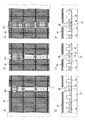
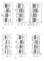
- FIG. 10 is an explanatory diagram of a method of manufacturing an EL display panel according to the present invention in the first embodiment.
- FIG. 11 is explanatory drawing of the manufacturing apparatus of EL display panel of this invention.
- the TFT substrate 52 is disposed in a vacuum state such as the vapor deposition chamber 56.
- Each organic film constituting the EL element 22 is formed by vapor deposition.
- the TFT substrate 52 is carried into the film forming apparatus 116 from the carry-in chamber 113.
- the inside of the film forming apparatus 116 is maintained in an ultra vacuum state.
- a central chamber 115 is provided at the central portion of the film forming apparatus 116, and a transfer robot (not shown) that carries TFTs into or out of the chamber chambers 111 is installed in the central chamber 115. ing.
- the transfer robot unloads the moving stage 51 and the like from the chamber chamber 111, changes the direction, and loads it into the chamber chamber 111 of the next process.
- the laser device 58 for modifying the light emitting layer 17 and the like is installed in the laser device chamber 118, and the TFT substrate 52 is carried into the laser device chamber 118 via a load lock chamber (LL). .
- the TFT substrate 52 is unloaded from the unloading chamber 114 after the cathode electrode 19 is formed or after sealing with the sealing film 20 and the sealing film 27.
- the TFT substrate 52 is carried in from the carry-in chamber 113 and carried into a chamber (HTL) 111 c in which the hole transport layer 16 is deposited. In the chamber chamber 111c, the hole transport layer 16 is formed above the pixel electrode 15 of the TFT substrate 52 as shown in FIGS. 10A and 11A.
- the TFT substrate 52 is carried into a chamber chamber (EML (R)) 111d for depositing the light emitting layer (EML) R.
- EML chamber chamber
- the light emitting layer 17R is laminated on the hole transport layer 16 by a vapor deposition method.
- the light emitting layer 17R is formed by co-evaporating a host material and a red guest material.
- the fine vapor deposition mask 251R in which the opening is provided at the position corresponding to the pixel 37R is not used.
- the light emitting layer 17R is formed as a continuous film on the entire display screen 36 by using a vapor deposition method.
- the light emitting layer 17R is formed continuously and continuously in common with the pixel electrode 15R, the pixel electrode 15G, and the pixel electrode 15B.
- a rough vapor deposition mask (not shown) having an opening in the display screen 36 is used so that the light emitting layer 17R is vapor deposited in the display screen 36.
- a bank 95 is shown in the EL display panel, but the bank 95 is not necessarily a necessary component.
- the bank 95 is formed on the source signal line 35, the gate signal line 34, and the periphery of the pixel electrode 15, and exhibits an electric field shielding effect.
- the bank is made of a material that adds pigments and dyes that absorb visible light.
- the direction of the TFT substrate 52 is changed by the transfer robot in the central chamber 115 and is carried into the laser device chamber 118 via the load lock chamber 112. In the laser device chamber 118, as shown in FIG. 10B, the light emitting layer 17 of the TFT substrate 52 is irradiated with laser light 59a.
- the laser light 59a is applied to the light emitting layer 17R above the pixel electrode 15G and the pixel electrode 15B.
- the laser light 59a is not applied to the light emitting layer 17R above the pixel electrode 15R.
- the light emitting layer 17R is modified by the irradiated portion of the laser beam 59a to become a modified portion 96a.
- the guest material of the light emitting layer 17R above the pixel electrode 15G and the pixel electrode 15B absorbs the laser light 59a, and the covalent bond chain is cut.
- the radical of the covalent chain generates a double bond, pulls out and bonds an atom of another covalent chain, or crosslinks with another covalent chain.
- the structure changes.
- the guest material of the light emitting layer 17R corresponding to the pixel electrode 15R is not irradiated with the laser beam 59a. Therefore, the performance as a guest material that emits light is maintained.
- each organic film forming the EL element 22 is described as being formed by a vapor deposition method, but the present invention is not limited to this.
- the electron transport layer 18, the hole transport layer 16, the light emitting layer 17, and the like may be formed by an ink jet method or a printing method.
- the light emitting layer 17 is formed as the light emitting layer 17 above the pixel electrode 15 by an inkjet method in which a host material and a guest material are dissolved in a solvent.
- a method of forming the light emitting layer 17R by the ink jet method and modifying the light emitting layer 17R by irradiating the light emitting layer 17R or a configuration of an EL display panel (device) is also a technical category of the present invention.
- the guest material mainly absorbs light and the light emitting layer 17 is modified.
- the present invention is not limited to this.
- the light-emitting layer 17 is formed of a single organic film such as Alq 3
- a method for irradiating the single organic film with light to modify the single organic film or an EL display panel The configuration of (apparatus) is also a technical category of the present invention.
- a method or an EL display panel (device) in which a hole transport layer or the like is irradiated with a laser beam 59 for modification is also a technical category of the present invention.
- the laser beam 59 is ultraviolet light having a wavelength ⁇ of 300 nm or more and 420 nm or less. More preferably, the laser light 59 is ultraviolet light having a wavelength ⁇ of 310 nm or more and 400 nm or less.
- the TFT substrate 52 is carried into the central chamber 115 via the load lock chamber 112 and carried into the chamber chamber (EML (G)) 111b.
- the chamber chamber 111b as shown in FIG. 10C, the light emitting layer 17G is laminated on the light emitting layer 17R by a vapor deposition method.
- the fine vapor deposition mask 251 is not used in the vacuum vapor deposition step of the light emitting layer 17G.
- the light emitting layer 17G is vapor-deposited on the display screen 36 of the display panel using a rough vapor deposition mask (not shown). Accordingly, the light emitting layer 17G is formed in common above the pixel electrode 15R, the pixel electrode 15G, and the pixel electrode 15B.
- the direction of the TFT substrate 52 is changed by the transfer robot in the central chamber 115 and is carried into the laser device chamber 118 via the load lock chamber 112.
- the light emitting layer 17G of the TFT substrate 52 is irradiated with laser light 59b.
- the laser light 59b irradiates the light emitting layer 17G above the pixel electrode 15B.
- the laser light 59b is not applied to the light emitting layer 17G above the pixel electrode 15R and the pixel electrode 15G.
- the light emitting layer 17G is modified by the irradiated portion of the laser beam 59b to become a modified portion 96b.
- the guest material of the light emitting layer 17G often has higher excitation energy than the guest material of the light emitting layer 17R.
- a guest material having a large excitation energy may have a short wavelength to be absorbed.
- a laser beam having a shorter wavelength than the laser beam 59a is selected as the wavelength of the laser beam 59b.
- the laser beam 59b is ultraviolet light having a wavelength ⁇ of 300 nm to 380 nm.
- the laser beam 59a is ultraviolet light having a wavelength ⁇ of 310 nm to 400 nm.
- the wavelengths of the laser light 59a and the laser light 59b are the same, and the intensities per unit area of the laser light 59a and the laser light 59b are made different.
- the light emitting layer 17G above the pixel 37B absorbs and modifies the laser light 59b.
- the light emitting layer 17G above the pixel 37B serves as a modified portion 96b. Therefore, the guest material of the light emitting layer 17G is modified and cannot be excited.
- the light emitting layer 17G functions as a host material.
- the light emitting layer 17R above the pixel electrode 15G is described as a modified portion 96a
- the light emitting layer 17G above the pixel electrode 15B is described as a modified portion 96b.
- the modified portion 96a and the modified portion 96b are different in guest materials and often have different physical or physical properties. However, the reforming part 96a and the reforming part 96b often have the same or similar physical properties. Accordingly, the reforming unit 96a and the reforming unit 96b may be the same as the reforming unit 96.
- the TFT substrate 52 is carried into the chamber chamber (EML (B) ETL) 111e via the central chamber 115.
- the light emitting layer 17B is stacked above the light emitting layer 17G.
- the light emitting layer 17B material is vapor deposited by laminating a host material and a blue light emitting guest material on the light emitting layer 17G by vacuum vapor deposition in vacuum.
- the fine vapor deposition mask 251 is not used in the vacuum vapor deposition step of the light emitting layer 17B.
- the light emitting layer 17B is deposited on the entire display screen 36 of the display panel using a rough deposition mask (not shown). Therefore, the light emitting layer 17B is formed in common above the pixel electrode 15R, the pixel electrode 15G, and the pixel electrode 15B.
- an electron transport layer 18 is formed above the light emitting layer 17B, and subsequently, LiF or Liq or the like as an electron injection layer is formed, and the cathode electrode 19 is placed on the electron transport layer 18. Laminate to.
- the cathode electrode 19 is made of aluminum, silver, a silver / magnesium (MgAg) alloy, calcium, or the like.
- the cathode electrode 19 is laminated above the light emitting layer 17B by, for example, vacuum deposition. In this vacuum deposition, a rough deposition mask is used so that the cathode electrode material is deposited on the display area of the EL display panel. As a result, the cathode electrode 19 is formed as a continuous film over the entire display area.
- the cathode electrode (cathode) 19 is formed, a film forming method in which the energy of the film forming particles is small enough not to affect the base, such as vapor deposition or CVD.
- the sealing film 20 is formed by the method.
- the film forming temperature is set to a range of 15 ° C. to 25 ° C., which is close to normal temperature.
- an acrylic or epoxy organic material or the like may be formed to form the sealing film 20. It is preferable to stick a sealing film 27 on the sealing film 20 and take a moisture-proof measure.
- the TFT substrate 52 and the sealing substrate are bonded to each other through the sealing layer so that the EL display element is surrounded by the TFT substrate 52, the sealing substrate, and the sealing layer.
- the TFT substrate 52 is sealed with a thin film sealing technique. In the thin film sealing technique, an extremely thin inorganic film and organic film are laminated on the TFT substrate 52 in a multilayer manner.
- the inorganic film mainly protects the EL element 22 by preventing intrusion of oxygen and moisture.
- the TFT substrate 25 is unloaded from the film forming apparatus 116 via the unloading chamber 114.
- a circularly polarizing plate (circularly polarizing film) 29 is attached or disposed on the light emission side of the EL display panel in order to improve the display contrast.
- the laser device that generates the laser light 59a and the laser device 58 that generates the laser light 59b are installed, but the present invention is not limited to this.
- the laser beam 59a and the laser beam 59b may be generated by a single laser device 58 that generates light having a variable wavelength. Needless to say, a plurality of laser devices 58 that generate either the laser beam 59a or the laser beam 59b may be installed.
- the laser beam 59a and the laser beam 59b may have different wavelengths.
- the light emitting layer 17 is formed and then the laser light 59 is irradiated to modify the light emitting layer 17, but the present invention is not limited to this.
- the light emitting layer 17 may be modified or removed by irradiating the laser beam 59 while forming the light emitting layer 17 by vapor deposition.
- pixels 37 of a plurality of colors are arranged in a matrix.
- a light emitting layer 17a of the first color is formed on a pixel of at least one color, and a light emitting layer 17b of the second color is formed thereon.
- the emission wavelength of the first color emission layer 17a is longer than the emission wavelength of the second color emission layer 17b.
- the guest material of the light emitting layer 17a of the first color absorbs energy excited by the light emitting layer 17b of the second color and emits light.
- the light emitting layer 17a of the first color is formed on at least one color pixel, and the light emitting layer 17b of the second color is formed thereon.
- the light emitting layer 17a of the first color is irradiated with light having a narrow directivity such as a laser beam 59 to modify the light emitting layer 17a of the first color to make a non-light emitting layer.
- the light emitting layer 17b of the second color emits light.
- the red light emitting layer 17R is modified by modifying the red light emitting layer 17R. No light is emitted, only the green light emitting layer 17G emits light, and the pixel 37 having the pixel electrode 15 emits green light.
- the present invention is not limited to an EL display panel in which a plurality of color pixels 37 are arranged in a matrix.
- a plurality of light emitting portions are formed on the display portion or the display screen 36, and a plurality of light emitting layers 17 are laminated on the light emitting portions.
- the long wavelength light emitting layer 17 is irradiated with narrow directivity light such as laser light 59 without using the fine vapor deposition mask 251, so that the long wavelength light emitting layer 17 is modified. It is characterized by being quality.
- the fine vapor deposition mask 251 is not used when forming at least one of the light emitting layers 17 in order to form the light emitting layer 17R, the light emitting layer 17G, and the light emitting layer 17B.
- at least one of the light emitting layers 17 is irradiated with light having a narrow directivity ultraviolet wavelength such as the laser light 59.
- the irradiation position of the laser beam 59 can be controlled with high accuracy by the galvanometer mirror 62 or a moving stage (linear stage or the like).
- the positioning can be easily set in correspondence with the position of the pixel 37 on the TFT substrate 52. Therefore, EL display panels having different shapes of the pixels 37, the arrangement of the pixels 37, and the number of the pixels 37 can be easily manufactured by changing the product type. In addition, the equipment cost of the manufacturing apparatus is very low.
- the vapor deposition hole (mask opening) of the fine vapor deposition mask 251 becomes small, so that it is difficult to process the vapor deposition hole of the fine vapor deposition mask 251. is there. Further, there is a problem that it is difficult to position the fine vapor deposition mask 251 in accordance with the position of the pixel 37 of the EL display panel. In addition, the fine vapor deposition mask 251 used for manufacturing a large EL display panel for a television has a large area and is heavy. Accordingly, there is a problem that the transfer robot for positioning the fine vapor deposition mask 251 is also large.
- the emission color of the light emitting layer 17 is determined by irradiating the pixel 37 with the laser beam 59.
- the spot size of the laser light 59 having the ultraviolet wavelength can be 10 ⁇ m or less.
- the laser beam 59 can be positioned at high speed by the control of the galvanometer mirror 62. Even if the EL display panel size is a large area, the laser light 59 is controlled by the galvano mirror 62 or by moving the moving stage 51 etc. Even at the position, it can be positioned at high speed. Further, since positioning of the fine vapor deposition mask 251 is unnecessary and only the control of the laser beam 59 is required, the manufacturing equipment is inexpensive and the manufacturing tact time can be shortened. From the above, in the manufacturing method of the present invention, the EL display panel can be manufactured at low cost even if the pixel 37 has high definition and the EL display panel has a large area. Also, excellent display quality and high manufacturing yield can be realized.
- the light emitting layer 17 is modified by irradiating the light emitting layer 17 with the laser beam 59.
- the continuous light emitting layer 17 may be formed on the adjacent pixel 37, and the light emitting layer 17 may be removed by irradiating the light emitting layer 17 of the corresponding pixel 37 with the laser light 59.
- the light emitting layer 17R is laminated on the hole transport layer 16 on the TFT substrate 52.
- the light emitting layer 17R is formed as a light emitting layer 17R continuous to the red pixel 37R, the green pixel 37G, and the blue pixel 37B.
- the laser light 59a is irradiated to the light emitting layer 17R above the green pixel electrode 15G and the blue pixel electrode 15B.
- the light emitting layer 17R is heated and evaporated by irradiation with the laser beam 59a.
- the light emitting layer 17R is removed by evaporation.
- the light emitting layer 17G above the blue pixel electrode 15B is irradiated with laser light 59b.
- the light emitting layer 17G absorbs the laser beam 59b and is heated and evaporated.
- the light emitting layer 17G is removed from the hole transport layer 16 by evaporating.
- the three light emitting layers of the light emitting layer 17R, the light emitting layer 17G, and the light emitting layer 17G are stacked above the red pixel electrode 15R.
- Two light emitting layers of a light emitting layer 17G and a light emitting layer 17G are stacked above the green pixel electrode 15G.
- a light emitting layer 17G is stacked above the blue pixel electrode 15B.
- the light emitting layer 17R is evaporated and removed, but a part of the light emitting layer 17R may remain. However, since the remaining light emitting layer 17R is modified by the laser light 59a, it does not contribute to light emission.
- the light emitting layer 17G is removed by evaporation, but part of the light emitting layer 17G may remain. However, since the remaining light emitting layer 17G is modified by the laser light 59b, it does not contribute to light emission.
- the emission color of the pixel 37R is substantially equal to the emission color of the light emitting layer 17R, and the pixel 37R emits red light.
- recombination of electrons and holes mainly occurs in the light emitting layer 17G, but the recombination may also emit light in the light emitting layer 17B.
- the emission color of the pixel electrode 15G is substantially equal to the emission color of the light emitting layer 17G, and the pixel electrode 15G emits green light.
- the pixel 37B recombination of electrons and holes mainly occurs in the light emitting layer 17B. Since the light emitting layer 17 of the other color is removed, the pixel 37B emits blue light. Therefore, by removing the light emitting layer 17 with the laser light 59, an EL display panel having three primary colors of red, green, and blue can be manufactured.
- the laser device 58 is used to modify the light emitting layer 17.
- the present invention is not limited to this.
- an LED light-emitting diode
- an LED has a small light emitting element, it can generate light having a narrow directivity.
- FIG. 12 is an explanatory diagram of a light generator using the LED 122.
- FIG. 13 is explanatory drawing of the modification
- the substrate 123 of the light generator uses a metal plate or a ceramic plate as a base material in order to dissipate heat generated by the LEDs 122.
- a heat sink (not shown) is attached to the back surface of the substrate.
- An LED 122 that generates ultraviolet light is attached to the substrate 123.
- the size (vertical length c, horizontal length b) of the light emitting portion of the LED 122 is substantially matched with the size of the region of the pixel 37 to be modified.
- the size of the light emitting portion (vertical length c, horizontal length b) is made smaller than the size of the region of the pixel 37 to be modified.
- a lens (not shown) or the like may be disposed in front of the light emitting portion of the LED 122 so that substantially the entire pixel 37 can be irradiated with ultraviolet light generated by the LED 122.
- the LED 122 emits light
- the light emitting layer 17 formed above the pixel electrode 15 of the predetermined color of the pixel 37 can be modified.
- the mounting position E in the vertical direction of the LEDs 122 is matched with the pitch of the pixels 37.
- the mounting position d of the LED 122 in the horizontal direction is substantially matched with the column pitch of the pixels 37.
- the vertical mounting position e of the LED 122 and the horizontal mounting position d of the LED are set to N times the pixel pitch (N is a positive number of 1 or more).
- the length F in which the LEDs are mounted is the length from the first row to the last pixel row of the EL display panel. Therefore, the number of LEDs mounted on the length F matches the number of pixel rows of the EL display panel.
- the length F is set to 1 / N (N is a positive number of 1 or more) of the length from the first row to the last pixel row of the EL display panel.
- the LED 122 is mounted in two rows, but the present invention is not limited to this.
- the mounting rows of the LEDs 122 may be three or more.
- the number of mounting columns or mounting rows of the LEDs 122 may be the number of pixel columns or pixel rows of the display panel. In this case, it is not necessary to move the light generator in the direction a as shown in FIG. A light generator may be positioned on the EL display panel to cause the LED 122 to emit light.
- the wavelengths of light generated by the LEDs 122a and the LEDs 122b may be different.
- the LED 122a may generate light having the main wavelength of the laser light 59a described in FIG. 10
- the LED 122b may generate light having the main wavelength of the laser light 59b.
- FIG. 12B is a cross-sectional view taken along the line aa ′ of FIG. 12A.
- a light absorbing material 121 that absorbs the ultraviolet light generated by the LED 122 is formed around the LED 122.
- the LED 122a generates ultraviolet light 141a
- the LED 122b generates ultraviolet light 141b.
- Examples of the light absorbing material 121 include those obtained by adding carbon to acrylic or epoxy resin.
- the light generator is arranged so as to coincide with the position of the pixel electrode 15 of the TFT substrate 52.
- the light generator moves at a pixel column or pixel row pitch, and the LED 122 emits light at the moved position, thereby modifying the light emitting layer 17 of the pixel 37.
- both the LED 122a and the LED 122b emit light.
- one of the LEDs 122a or the LEDs 122b emits light.
- the light generating means for generating the ultraviolet light 59 is not limited to the laser device 58. Any means may be used as long as it is a light generating means capable of irradiating light such as ultraviolet light corresponding to the position of the pixel 37 without using the fine vapor deposition mask 251. Needless to say, the light generating means can be applied as a light generating source 58 of the thermal transfer apparatus shown in FIG. 18 or the like by using infrared light generating means.
- the LED 122 of the light generator can be used as the light generation source 58 of the thermal transfer apparatus shown in FIG. 18, FIG. 19, and FIG.
- the donor film 197 is disposed between the TFT substrate 52 and the light generator, and the transfer organic film 195 of the donor film 197 is overheated with the light generated by the light emitting LED 122 of the light generator,
- the light emitting layer 17 may be formed.
- the LED 122a of the light generator shown in FIG. 12A is an infrared light emitting LED and the LED 122b is an ultraviolet light emitting LED
- the light generator is configured as a device that combines the modification of the constituent material of the light emitting layer 17 and the thermal transfer. it can. Moreover, it can be used as a light generator for removing the deposit 201 described in FIG.
- the light generated by the LED 122 has a fixed wavelength band instead of a single wavelength like laser light. Therefore, as the light generated by the LED 122, light that generates ultraviolet light having a dominant wavelength of 310 nm to 400 nm is employed.
- FIG. 14 and 15 are a cross-sectional view of an EL display panel and an explanatory diagram of a manufacturing method according to the second embodiment of the present invention.
- a light emitting layer (EML (R)) 17R and a light emitting layer (EML (GB)) 17GB are formed above the red pixel electrode 15R.
- a light emitting layer (EML (R)) 17R and a light emitting layer (EML (GB)) 17GB are formed above the green pixel electrode 15G and the blue pixel electrode 15B.
- the light emitting layer (EML (GB)) 17 GB contains a blue guest material and a green guest material. The blue guest material and the green guest material have different wavelengths of light to be absorbed.
- the light emitting layer (EML (R)) 17R is modified by being irradiated with the laser light 59a. Further, the light emitting layer (EML (GB)) 17GB is irradiated with the laser beam 59b, and the blue guest material of the light emitting layer (EML (GB)) 17GB is modified.
- the blue pixel electrode 15B the light emitting layer (EML (R)) 17R is modified by being irradiated with the laser beam 59a. Further, the light emitting layer (EML (GB)) 17GB is irradiated with the laser light 59c, and the green guest material of the light emitting layer (EML (GB)) 17GB is modified.
- the TFT substrate 52 is carried in from the carry-in chamber 113 of FIG. 11A and carried into the chamber (HTL) 111c.
- the hole transport layer 16 is formed above the pixel electrode 15 of the TFT substrate 52.
- the TFT substrate 52 is carried into a chamber chamber (EML (R)) 111d for depositing the light emitting layer (EML) R.
- EML (R) chamber chamber
- the light emitting layer 17R is laminated on the hole transport layer 16 by a vapor deposition method.
- the light emitting layer 17R is formed by co-evaporating a host material and a red guest material.
- the light emitting layer 17R is formed as a continuous film on the entire display screen.
- the TFT substrate 52 is carried into the laser device chamber 118.
- the light emitting layer 17R of the TFT substrate 52 is irradiated with laser light 59a.
- the laser light 59a is applied to the light emitting layer 17R above the pixel electrode 15G and the pixel electrode 15B.
- the laser light 59a is not applied to the light emitting layer 17R above the pixel electrode 15R.
- the light emitting layer 17R is modified by the irradiated portion of the laser beam 59a to become a modified portion 96a.
- the TFT substrate 52 is carried into the central chamber 115 via the load lock chamber 112 and carried into the chamber chamber (EML (G)) 111b.
- a light emitting layer (EML (GB)) 17GB is stacked above the light emitting layer 17R.
- the light emitting layer (EML (GB)) 17 GB contains a blue guest material and a green guest material.
- the wavelength of the laser beam 59 to be absorbed is different between the blue guest material and the green guest material.
- a material that hardly absorbs the laser beam 59a, the laser beam 59b, and the laser beam 59c is selected as the host material.
- a material that transmits the laser beam 59 is selected.
- the concept that the material is difficult to absorb light such as laser light is that the material does not absorb the light, reflects light such as the laser light, or transmits light such as the laser light. To include. Further, it also includes that the material or its component does not change even when light such as laser light is absorbed.
- the guest material R a material that easily absorbs the laser beam 59a is selected.
- the guest material B a material that easily absorbs the laser beam 59b and hardly absorbs the laser beam 59c is selected.
- the guest material G a material that easily absorbs the laser beam 59c and hardly absorbs the laser beam 59b is selected.
- the material of the guest material G is selected so that the absorption rate of the guest material G is 25% or less when the absorption rate of the guest material B is 100% at the wavelength of the laser beam 59b. To do.
- the guest material B having an absorptivity of the guest material B of 25% or less is selected.
- the absorptance of the guest material B is 100% at the wavelength of the laser beam 59b
- a host material having an absorptivity of the host material of 25% or less is selected.
- An absorptivity of 100% may be read as 0% of transmittance, an absorptivity of 0% as 100% of transmittance, an absorptivity of 75% as 25% of transmittance, and an absorptivity of 25% as 75%.
- a light emitting layer (EML (GB)) 17GB is formed above the green pixel electrode 15G.
- the light emitting layer (EML (GB)) 17GB contains a guest material B that contributes to blue light emission and a guest material G that contributes to green light emission.
- the wavelength of the laser beam 59b is shorter than the wavelength of the laser beam 59c.
- the guest material B absorbs light having a shorter wavelength than the guest material G better.
- the guest material G of the light emitting layer (EML (GB)) 17 GB does not absorb the laser beam 59 b. Since the light emitting layer (EML (GB)) 17GB maintains the state in which the guest material G can emit light, the light emitting layer (EML (GB)) 17GB becomes the light emitting layer 17G that emits green light.
- a light emitting layer (EML (GB)) 17GB is formed above the blue pixel electrode 15B.
- the guest material G of the light emitting layer (EML (GB)) 17GB absorbs the laser light 59c and is modified.
- the guest material B does not absorb the laser beam 59b. Since the light emitting layer (EML (GB)) 17GB maintains the state in which the guest material B can emit light, the light emitting layer (EML (GB)) 17GB becomes the light emitting layer 17B that emits blue light.
- an electron transport layer 18 is formed above the light emitting layers 17G and B, subsequently, LiF or Liq is formed as an electron injection layer, and the cathode electrode 19 is replaced with the electron transport layer 18. Laminate on top. A cathode electrode 19 is formed on the electron transport layer 18.
- Most of the guest material included in the light emitting layer 17R above R of the pixel electrode 15R can emit light.
- the red guest material R included in the light emitting layer 17R above the pixel electrode 15G and the pixel electrode 15B is hardly quenched or excited.
- the blue guest material B included in the light emitting layer 17GB above the pixel electrode 15G is hardly quenched or excited by irradiation with the laser light 59b.
- the green guest material G included in the light emitting layer 17GB above the pixel electrode 15B is hardly quenched or excited by irradiation with the laser light 59c.
- the green guest material G and the blue guest material B can also be excited.
- the green guest material G of the light emitting layer 17GB absorbs energy for exciting the blue guest material B.
- the red guest material R included in the light emitting layer 17R above the pixel electrode 15R absorbs energy that excites the green guest material G and emits light.
- the contained red guest material R is not excited because it is irradiated with the laser beam 59a.
- the blue guest material B of the light emitting layer 17GB is not excited because it is irradiated with the laser beam 59b. Therefore, the light emitting layer 17GB emits green light. Therefore, the pixel 37 of the pixel electrode 15G emits green light.
- the green guest material G of the light emitting layer 17GB is a material that absorbs energy that excites the blue guest material B satisfactorily, or the EL element 22 has a configuration of the pixel electrode 15G.
- the green guest material G included in the upper light emitting layer 17GB absorbs the energy excited by the blue guest material B and emits light. Therefore, the light emitting layer 17GB emits green light. In this case, the step of irradiating the light emitting layer 17GB above the pixel electrode 15G with the laser light 59b in FIG. 15D can be eliminated.
- the contained red guest material R is not excited because it is irradiated with the laser light 59a.
- the green guest material G of the light emitting layer 17GB is not excited because it is irradiated with the laser beam 59c. Therefore, the light emitting layer 17GB emits blue light. Therefore, the pixel 37 of the pixel electrode 15B emits blue light.
- 16 and 17 are a cross-sectional view of an EL display panel and an explanatory view of a manufacturing method according to the third embodiment of the present invention.
- a light emitting layer 17R, a light emitting layer 17G, and a light emitting layer 17B are formed above the red pixel electrode 15R.
- a light emitting layer 17G and a light emitting layer 17B are formed above the green pixel electrode 15G and the blue pixel electrode 15B.
- the light emitting layer 17G above the blue pixel electrode 15B is irradiated with light to modify the green guest material of the light emitting layer 17G.
- the hole transport layer 16 is formed on the TFT substrate 52 above the pixel electrode 15.
- the TFT substrate 52 is carried into a chamber chamber (EML (R)) 111d for depositing the light emitting layer (EML) R.
- EML chamber chamber
- a fine vapor deposition mask 251R is disposed on the TFT substrate 52 in order to form the red light emitting layer 17R.
- the fine vapor deposition mask 251R is a mask having an opening at a red pixel position.
- the red light emitting layer material 172R is evaporated, and the light emitting layer 17R is laminated on the hole transport layer 16.
- the light emitting layer 17R is formed by co-evaporating a host material and a red guest material. Co-evaporation is performed in a vacuum process.
- the TFT substrate 52 is carried into the chamber chamber 111b.
- the light emitting layer 17G is laminated.
- the light emitting layer 17G contains a green guest material.
- the TFT substrate 52 is carried into the laser device chamber 118 shown in FIG. 11A.
- the light emitting layer 17G above the blue pixel electrode 15B is irradiated with the laser light 59.
- the guest material G of the light emitting layer 17G absorbs the laser beam 59 and is modified. Since the light emitting layer 17G above the green pixel electrode 15G is not irradiated with the laser light 59, the guest material G of the light emitting layer 17G is in a state capable of emitting light.
- a light emitting layer 17B is formed. Since the light emitting layer 17B maintains the state in which the guest material B can emit light, the light emitting layer 17B becomes a light emitting layer that emits blue light.
- the electron transport layer 18 is formed above the light emitting layer 17 GB, then the electron injection layer is formed, and the cathode electrode 19 is stacked on the electron transport layer 18.
- the light emitting layer 17 is formed using the fine vapor deposition mask 251, but the present invention is not limited to this.
- other layers such as the hole transport layer 16 may be formed using the fine vapor deposition mask 251.
- the step of forming the insulating film 14B is exemplified.
- recombination of electrons and holes mainly occurs in the red guest material R of the light emitting layer 17R, but the recombination occurs in the green guest material G and the light emission of the light emitting layer 17G. It may also occur in the blue guest material B of the layer 17B.
- the green guest material G of the light emitting layer 17G absorbs energy that excites the blue guest material B of the light emitting layer 17B.
- the red guest material R included in the light emitting layer 17R above the pixel electrode 15R absorbs energy that excites the green guest material G and emits light.
- the light emitting layer 17 of the pixel electrode 15R of the EL display panel of the present invention shown in FIG. 16 emits red light.
- the green guest material G of the light emitting layer 17G above the pixel electrode 15G absorbs energy that excites the blue guest material B of the light emitting layer 17B.
- the light emitting layer 17 of the pixel electrode 15G of the EL display panel of the present invention shown in FIG. 16 emits green light.
- the contained green guest material G is not excited by being irradiated with the laser light 59.
- the light emitting layer 17B emits blue light. Therefore, the pixel 37 of the pixel electrode 15B emits blue light.
- the formation of the light emitting layer 17 ⁇ / b> R with the fine vapor deposition mask 251 is described as an example, but the present invention is not limited to this.
- the light emitting layer 17R may be formed by a laser thermal transfer method, an ink jet method, or a printing method. It is also a technical category of the present invention to form other light emitting layers such as the light emitting layer 17G and the light emitting layer 17B with a fine vapor deposition mask.
- FIG. By forming the hole transport layer 16 using the fine vapor deposition mask 251, for example, as shown in FIG. 1, the film thicknesses of the hole transport layer 16R, the hole transport layer 16G, and the hole transport layer 16B are increased. Can be easily modified and formed.
- FIG. 18 is an explanatory diagram of a laser thermal transfer apparatus which is one of the EL display panel manufacturing apparatuses of the present invention. Items related to the laser device 58 of the laser thermal transfer device, the control device, the control method, the operation, and the like have been described with reference to FIGS.
- the laser light 59 generated by the laser device 58 is light in the ultraviolet region when modifying the light emitting layer 17 and the like, whereas it is different from light in the infrared region in the case of laser thermal transfer.
- FIG. 11B is an explanatory diagram of an EL display panel manufacturing apparatus according to the fourth embodiment of the present invention.
- the laser thermal transfer device is disposed in the transfer device chamber 117 of FIG. 11B.
- the TFT substrate 52 is carried into the transfer device chamber 117 via the load lock chamber 112a.
- 11A and 11B is that the chamber chamber 111d is a load lock chamber 112a and a transfer device 117.
- the transfer device for the transfer organic film 195 includes a laser device 58 that generates a laser beam 59d that irradiates the donor film 197.
- FIG. 19 is an explanatory diagram for explaining the operation of irradiating the donor film 197 with the laser beam 59d by the laser device 58 in the transfer process.
- the laser thermal transfer apparatus includes a moving stage 182 on which the TFT substrate 52 is placed and a control mechanism 185.
- the support mechanism 183 of the control mechanism 185 holds the donor film 197 disposed on the TFT substrate 52.
- the support mechanism 183 includes an elevating mechanism 184 so that the distance between the TFT substrate 52 and the donor film 197 can be adjusted.
- the moving stage 182 has an exhaust port 181 for exhausting the gas existing between the TFT substrate 52 and the donor film 197 to the outside.
- the control mechanism 185a includes a support mechanism 183a that supports one end of the donor film 197 and an elevating mechanism 184a.
- the control mechanism 185b includes a support mechanism 183b that supports the other end of the donor film 197 and an elevating mechanism 184b.
- the support mechanism 183a and the support mechanism 183b can move the donor film 197 up and down on the moving stage 182 independently.
- the elevating mechanism 184a moves up and down on the moving stage 182.
- the support mechanism 183b fixes the other end of the donor film 197.
- the elevating mechanism 184 b moves the donor film 197 up and down on the moving stage 182.
- the support mechanism 183 supports the donor film 197 so that the donor film 197 is disposed on the TFT substrate 52.
- the support mechanism 183 and the elevating mechanism 184 can support both ends of the donor film 197 and move the donor film 197 up and down with respect to the TFT substrate 52.
- the moving stage 182 includes two exhaust ports 181a and 181b.
- the exhaust port 181 is a passage that connects the inside and outside of the transfer device chamber 117.
- the gas existing between the TFT substrate 52 placed on the moving stage 182 and the donor film 197 disposed on the TFT substrate 52 through the exhaust port 181 is exhausted to the outside of the transfer device chamber 117.
- the moving stage 182 further includes driving means (not shown) for moving. For example, when the laser beam 59 is irradiated in the normal direction of the TFT substrate 52, a driving unit (mechanism) for moving the moving stage 182 in the lateral direction is provided.
- the support mechanism 183 can be raised or lowered in the normal direction of the TFT substrate 52 by the lifting mechanism 184.
- the control mechanism 185a and the control mechanism 185b can be independently controlled in operation, and can be controlled to rise and fall independently.
- the pressure roller 186 is disposed on the donor film 197 and can apply pressure on the donor film 197 toward the TFT substrate 52.
- the pressure roller 186 applies pressure to the donor film 197 toward the TFT substrate 52 during the bonding process between the donor film 197 and the TFT substrate 52, thereby bringing the donor film 197 and the TFT substrate 52 into close contact with each other.
- the pressure roller 186 can prevent the transfer organic film 195 transferred to the TFT substrate 52 from being peeled off during the peeling process between the donor film 197 and the TFT substrate 52.
- the support mechanism 183 moves the donor film 197 so as to be separated from the TFT substrate 52 before the bonding step between the TFT substrate 52 and the donor film 197.
- the exhaust port 181 exhausts gas existing in the space between the TFT substrate 52 and the donor film 197 to the outside.
- the support mechanism 183 pulls in a direction extending from one end and the other end of the donor film 197 to the outside. By pulling the donor film 197, the support mechanism 183 prevents the donor film 197 from sagging toward the TFT substrate 52.
- the support mechanism 183 a lifts one end of the donor film 197, so that the pressure roller 186 is opposed to one end from one end of the donor film 197. Move along. By applying pressure to the donor film 197 by the pressure roller 186, it is possible to prevent the transfer organic film 195 transferred to the TFT substrate 52 from being peeled off during the peeling process.
- the support mechanism 183a is raised while the support mechanism 183b is stopped.
- the TFT substrate 52 is separated from one end of the donor film 197 from the side close to the support mechanism 183a.
- the support mechanism 183b starts to rise.
- the donor film 197 the donor film 197 closer to the support mechanism 183b is raised, and the donor film 197 and the TFT substrate 52 are separated.
- the manufacturing method of the EL display panel in the fourth embodiment of the present invention uses a laser thermal transfer method.
- the step of disposing the TFT substrate 52 on the moving stage 182, the step of removing the gas existing between the TFT substrate 52 and the donor film 197, and the bonding of the donor film 197 and the TFT substrate 52 are performed.
- a step, a step of transferring the transfer organic film 195 of the donor film 197 to the TFT substrate 52, and a step of peeling the donor film 197 and the TFT substrate 52 are performed.
- FIG. 19 is an explanatory diagram for explaining a configuration of a donor film 197 used in the fourth embodiment of the present invention and a manufacturing method using the donor film 197.
- the base film 191 of the donor film 197 is made of a transparent polymer material. As the base film 191, it is particularly preferable to use a polyethylene terephthalate film. The thickness of the base film 191 is preferably 10 ⁇ m to 500 ⁇ m.
- the base film 191 which comprises the donor film 197 is demonstrated as a film which consists of resin materials, this invention is not limited to this. Needless to say, the base film 191 may be formed of an inorganic material plate such as glass. Therefore, the donor film is not limited to a film, and may be any component as long as it is a sheet-like material on which the optical conversion film 192 and the transfer organic film 195 are formed.
- An optical conversion film 192 is formed on the base film 191.
- the optical conversion film 192 is a layer that absorbs the laser light 59d in the infrared-visible light region and converts part of the light into heat.
- Examples of the optical conversion film 192 include a metal film containing aluminum oxide and aluminum sulfide as a light-absorbing substance, carbon black, and graphite.
- An intermediate film 193 can be formed on the optical conversion film 192.
- the intermediate film 193 serves to prevent the light-absorbing substance contained in the optical conversion film 192, such as carbon black, from contaminating the transfer organic film 195 formed in the subsequent process.
- the intermediate film 193 can be formed of an acrylic resin or an alkyd resin.
- the intermediate film 193 is formed on the optical conversion film 192, it is preferable to further form a buffer film 194 on the intermediate film 193.
- the buffer film 194 is formed to prevent damage to the organic film formed on the transfer organic film 195 and to effectively adjust the adhesive force between the intermediate film 193 and the transfer organic film 195.
- the buffer film 194 is made of metal or metal oxide having a laser beam transmittance of 20% or less, and the thickness of the buffer film 194 is 0.05 ⁇ m or more and 1 ⁇ m or less.
- a transfer organic film 195 is formed on the buffer film 194.
- the transfer organic film 195 is an organic material for forming the light emitting layer 17, the hole injection layer, the hole transport layer 16, the electron injection layer, the electron transport layer 18, and the like.
- the transfer organic film 195 is manufactured by coating an organic thin film forming material. As the transfer organic film 195, two or more organic layers can be laminated as needed instead of one organic layer.
- the donor film 197 is irradiated with laser light 59d having an infrared wavelength or a visible wavelength.
- the light emitting layer 17R of the pixel 37R is exemplified and described by thermal transfer, but the present invention is not limited to this. Needless to say, the light emitting layers 17 of the pixels 37 of other colors may be formed.
- the formation by thermal transfer is not limited to the light emitting layer 17, and it goes without saying that another organic film such as the hole transport layer 16 may be formed.
- a donor film 197 is disposed on the TFT substrate 52.
- the alignment between the TFT substrate 52 and the donor film 197 is performed by a control mechanism 185 or the like.
- the laser beam 59d passes through the base film 191 and heats the optical conversion film 192.
- the optical conversion film 192 emits heat by the laser beam 59d.
- the optical conversion film 192 expands, and the transfer organic film 195 peels from the donor film 197.
- the peeled transfer organic film 195a is laminated as the light emitting layer 17R above the pixel electrode 15 of the TFT substrate 52.
- the thickness of the laminated light emitting layer 17 is proportional to the thickness of the transfer organic film 195.
- the thickness of the transfer organic film 195 can be defined.
- a plurality of donor films 197 may be used and the transfer organic film 195 may be transferred onto the hole transport layer 16 a plurality of times.
- the film thickness of the light-emitting layer 17 can be accurately formed to a prescribed film thickness by transferring a plurality of times.
- the laser beam 59d all general-purpose laser beams such as solid, gas, semiconductor, and dye can be used. Among these, it is preferable to use laser light having a wavelength in the infrared region having a wavelength of 800 nm or more.
- a YAG laser, a glass laser, and a carbon dioxide laser are exemplified.
- a helium neon (He—Ne) laser can also be employed.
- FIG. 11B and FIG. 21 are explanatory views of the EL display panel manufacturing method and manufacturing apparatus in the fourth embodiment.
- the TFT substrate 52 is carried into the film forming apparatus 116 from the carry-in chamber 113.
- a thermal transfer device that thermally transfers the light emitting layer 17 is installed in the transfer device chamber 117.
- the TFT substrate 52 is carried into the transfer device chamber 117 via the load lock chamber 112a.
- the TFT substrate 52 is carried into a chamber (HTL) chamber 111 c in which the hole transport layer 16 is deposited.
- the hole transport layer 16 is formed above the pixel electrode 15 of the TFT substrate 52.
- the TFT substrate 52 is carried into a transfer device chamber 117 to which the light emitting layer R is transferred.
- the donor film 197 is irradiated with laser light 59d having a wavelength in the infrared region or the visible light region.
- the laser beam 59d passes through the base film 191 and heats the optical conversion film 192.
- the released heat causes the optical conversion film 192 of the donor film 197 to expand, and the transfer organic film 195a peels from the donor film 197.
- the peeled transfer organic film 195 is transferred onto the hole transport layer 16 of the TFT substrate 52 to a desired pattern and thickness as the light emitting layer 17R.
- the transfer organic film 195a becomes the light emitting layer 17R.
- the transfer organic film 195 is thermally transferred to the TFT substrate 52 as the light emitting layer 17R.
- the transfer organic film 195 may adhere as an adherent 201b on the bank 95 as well as above the red pixel electrode 15R.
- the adhering material 201a is attached not only to the red pixel electrode 15R but also above the green pixel electrode 15G and above the blue pixel electrode 15B.
- the deposit 201b adhering to the bank 95 peels off and adheres to the pixel electrode 15 to cause a defect.
- the adhering material 201a attached above the green pixel electrode 15G and above the blue pixel electrode 15B emits light, which may cause a color mixing problem.
- FIG. 20 is an explanatory view of a method for modifying or removing the deposit 201 generated in the manufacturing process of the EL display panel of the present invention.
- the deposit 201 adhered to unnecessary portions by thermal transfer is irradiated with a laser beam 59a to be modified.
- the deposit 201 is irradiated with laser light 59a in the ultraviolet band.
- the guest material of the deposit 201 is modified by irradiation with laser light 59a having an ultraviolet wavelength. Due to the modification, the deposit 201 does not emit light or is removed.
- the laser beam 59a can be the same as the laser beam 59 in FIG.
- the same laser device 58 can be used.
- the wavelength of the laser beam 59a is in the ultraviolet region.
- the deposit 201 is modified by the irradiation of the laser beam 59a. Alternatively, the deposit 201 is heated and evaporated by irradiation with the laser beam 59 a, and is removed from above the pixel electrode 15.
- the TFT substrate 52 is carried into the chamber chamber (EML (G)) 111b.
- the chamber chamber 111b as shown in FIG. 21C, the light emitting layer 17G is laminated above the light emitting layer 17R by a vapor deposition method.
- the fine vapor deposition mask 251 is not used in the vacuum vapor deposition step of the light emitting layer 17G.
- the light emitting layer 17G is deposited on the entire display screen 36 of the display panel using a rough deposition mask (not shown). Accordingly, the light emitting layer 17G is formed in common above the pixel electrode 15R, the pixel electrode 15G, and the pixel electrode 15B.
- the TFT substrate 52 is carried into the laser device chamber 118 via the load lock chamber 112b.
- the light emitting layer 17G of the TFT substrate 52 is irradiated with laser light 59a.
- the laser light 59a irradiates the light emitting layer 17G above the pixel electrode 15B.
- the laser light 59a is not applied to the light emitting layer 17G above the pixel electrode 15R and the pixel electrode 15G.
- the light emitting layer 17G is modified by the irradiated portion of the laser light 59a to become a modified portion 96b. Since the light emitting layer 17G corresponding to the pixel electrode 15R and the pixel electrode 15G is not irradiated with the laser light 59a, the performance as the light emitting layer is maintained.
- the TFT substrate 52 is carried into a chamber chamber (EML (B) ETL) 111e.
- EML (B) ETL a chamber chamber
- the light emitting layer 17B is laminated above the light emitting layer 17G by a vapor deposition method.
- the fine vapor deposition mask 251 is not used in the vacuum vapor deposition step of the light emitting layer 17B.
- the light emitting layer 17B is deposited on the entire display screen 36 of the display panel using a rough deposition mask (not shown). Therefore, the light emitting layer 17B is formed in common above the pixel electrode 15R, the pixel electrode 15G, and the pixel electrode 15B.
- the electron transport layer 18 is formed above the light emitting layer 17 ⁇ / b> B, and then the electron injection layer is formed, and the cathode electrode 19 is stacked on the electron transport layer 18.
- the panel structure manufactured by the EL display panel manufacturing method described in FIG. 21 is the same as that in FIG. Since the structure and operation of the EL display panel in FIG. 16 have been described, description thereof will be omitted.
- the fourth embodiment is different in that the light emitting layer 17 of FIG. 16 is formed by a thermal transfer method.
- the formation of the light emitting layer 17R using the donor film 197 or the like has been described as an example.
- the present invention is not limited to this.
- it is also a technical category of the present invention to form other light emitting layers such as the light emitting layer 17G and the light emitting layer 17B with the donor film 197 or the like.
- FIG. By forming the insulating film 14 using the donor film 197 or the like, for example, as shown in FIG. 1, the thicknesses of the insulating film 14R, the insulating film 14G, and the insulating film 14B can be easily set.
- FIG. 22 and 23 are a cross-sectional view of an EL display panel and an explanatory view of a manufacturing method according to the fifth embodiment of the present invention.
- a light emitting layer 17R and a light emitting layer EML (GB) are formed above the red pixel electrode 15R.
- a light emitting layer EML (GB) is formed above the green pixel electrode 15G and the blue pixel electrode 15B.
- the light emitting layer EML (GB) is formed by co-evaporating a host material, a green light emitting guest material, and a blue light emitting guest material.
- the hole transport layer 16 is formed on the TFT substrate 52 above the pixel electrode 15.
- a fine vapor deposition mask 251R is disposed on the TFT substrate 52 in order to form the red light emitting layer 17R.
- the red light emitting layer material 172R is evaporated, and the light emitting layer 17R is laminated on the hole transport layer 16.
- the light emitting layer 17R is formed by co-evaporating a host material and a red guest material.
- a light emitting layer EML (GB) is stacked.
- the light emitting layer EML (GB) contains a green light emitting guest material and a blue light emitting guest material.
- the light emitting layer EML (GB) is formed by co-evaporating a host material, a green light emitting guest material, and a blue light emitting guest material.
- the TFT substrate 52 is carried into the laser device chamber 118, and as shown in FIG. 23D, the light emitting layer EML (GB) above the blue pixel electrode 15B is irradiated with the laser light 59c.
- the green guest material G in the light emitting layer EML (GB) absorbs the laser beam 59 c and becomes the modified portion 96.
- a material that hardly absorbs the laser beam 59c is selected as the host material and the green guest material B.
- the green guest material G a material that easily absorbs the laser light 59c is selected.
- the guest material B is selected such that the absorption rate of the guest material B is 25% or less when the absorption rate of the guest material G is 100% at the wavelength of the laser beam 59c.
- the material is selected so that the difference between the absorption rate of the guest material G and the absorption rate of the guest material B is three times or more. Since the light emitting layer 17G above the green pixel electrode 15G is not irradiated with the laser light 59c, the guest material G of the light emitting layer 17G is in a state capable of emitting light.
- the electron transport layer 18 is formed above the light emitting layer EML (GB), the electron injection layer is formed as illustrated in FIG. 23F, and the cathode electrode 19 is connected to the electron transport layer. 18 is laminated.
- the absorption spectrum of the red guest material R included in the light emitting layer 17R above the pixel electrode 15R in FIG. 22 at least partially overlaps the emission spectrum of the green guest material in the light emitting layer EML (GB). Further, the emission spectrum of the green guest material of the light emitting layer EML (GB) at least partially overlaps the emission spectrum of the blue guest material B of the light emitting layer EML (GB).
- recombination of electrons and holes mainly occurs in the red guest material R of the light emitting layer 17R, but recombination occurs in the green guest material G and blue of the light emitting layer EML (GB). This may also occur in the guest material B.
- the green guest material G of the light emitting layer EML (GB) absorbs energy for exciting the blue guest material B.
- the red guest material R included in the light emitting layer 17R above the pixel electrode 15R absorbs energy that excites the green guest material G and emits light.
- the light emitting layer 17R of the pixel electrode 15R of the EL display panel of the present invention shown in FIG. 22 emits red light.
- recombination of electrons and holes mainly occurs in the green guest material G of the light emitting layer 17G, but recombination occurs in the blue guest material of the light emitting layer EML (GB). It may also occur in the blue guest material B of B.
- the green guest material G of the light emitting layer EML (GB) absorbs energy that excites the blue guest material B of the light emitting layer EML (GB).
- the light emitting layer EML (GB) of the pixel electrode 15G of the EL display panel of the present invention shown in FIG. 22 emits green light.
- the contained green guest material G is not excited by being irradiated with the laser beam 59c.
- the blue guest material B emits light. Therefore, the pixel 37 of the pixel electrode 15B emits blue light.
- an emission layer EML is formed above the red, green, and blue pixel electrodes 15.
- the light emitting layer EML is formed by co-evaporating a host material, a red light emitting guest material, a green light emitting guest material, and a blue light emitting guest material.
- the hole transport layer 16 is formed on the TFT substrate 52 above the pixel electrode 15.
- the light emitting layer 17RGB is laminated on the hole transport layer 16 on the TFT substrate 52.
- the light emitting layer 17RGB is formed by co-evaporating a host material, a red light emitting guest material, a green light emitting guest material, and a blue light emitting guest material.
- the TFT substrate 52 is carried into the laser device chamber 118, and as shown in FIG. 25C, the laser light 59a is applied to the light emitting layer EML (RGB) above the green pixel electrode 15G and the blue pixel electrode 15B. Irradiated.
- the red guest material R in the light emitting layer EML (RGB) absorbs the laser beam 59a and becomes the modified portion 96a.
- a material that easily absorbs the laser light 59a is selected as the red guest material R.
- the green guest material G and the blue guest material B materials that hardly absorb the laser light 59a are selected.
- FIG. 25C the laser light 59a is applied to the light emitting layer EML (RGB) above the green pixel electrode 15G and the blue pixel electrode 15B. Irradiated.
- the red guest material R in the light emitting layer EML (RGB) absorbs the laser beam 59a and becomes the modified portion 96a.
- a material that easily absorbs the laser light 59a is selected
- the guest material G is selected such that the absorption rate of the guest material G is 25% or less when the absorption rate of the guest material R is 100% at the wavelength of the laser beam 59a. Further, the material is selected so that the difference between the absorption rate of the guest material R and the absorption rate of the guest material G is three times or more. The material is preferably selected so as to be 4 times or more. Since the light emitting layer 17R above the red pixel electrode 15R is not irradiated with the laser light 59a, the guest material R, the guest material G, and the guest material B of the light emitting layer 17RGB are in a state capable of emitting light.
- laser light 59b is applied to the light emitting layer EML (RGB) above the blue pixel electrode 15B.
- the green guest material G of the light emitting layer EML (RGB) absorbs the laser beam 59b and becomes the modified portion 96b.
- a green guest material G is selected as a material that easily absorbs the laser light 59b.
- a material that hardly absorbs the laser beam 59b is selected.
- the guest material B is selected such that the absorptance of the guest material B is 25% or less when the absorptivity of the guest material G is 100% at the wavelength of the laser beam 59b. Further, the material is selected so that the difference between the absorption rate of the guest material G and the absorption rate of the guest material B is three times or more.
- an electron transport layer 18 is formed above the light emitting layer EML (RGB), an electron injection layer is formed as shown in FIG. 25F, and the cathode electrode 19 is connected to the electron transport layer. 18 is laminated.
- EML light emitting layer
- EML red guest material
- EML light emitting layer
- the red guest material R included in the light emitting layer EML (RGB) above the pixel electrode 15R emits light by absorbing energy excited by the green guest material G.
- the light emitting layer 17R of the pixel electrode 15R of the EL display panel of the present invention shown in FIG. 24 emits red light.
- the green guest material G of the light emitting layer EML (RGB) above the pixel electrode 15G absorbs energy that excites the blue guest material B of the light emitting layer EML (RGB).
- the light emitting layer EML (RGB) of the pixel electrode 15G of the EL display panel of the present invention shown in FIG. 24 emits green light.
- the green guest material G contained in the light emitting layer EML (RGB) above the pixel electrode 15B is not excited by being irradiated with the laser light 59b.
- the red guest material R contained in the light emitting layer EML (RGB) is not excited by being irradiated with the laser light 59a.
- the blue guest material B emits light. Therefore, the pixel 37 of the pixel electrode 15B emits blue light.
- the light emitting layer 17 and the like above the pixel electrode 15 are irradiated with the laser light 59 to modify the light emitting layer 17 and the like.
- the present invention is not limited to this.
- the light emitting layers 17 of different colors overlap between adjacent pixels, color mixing occurs.
- the overlapping light emitting layer may generate red light and green light, and mixed color light may be generated.
- the light emitting layer 17 and the like may be modified or removed by irradiating laser light 59 between the pixels 37.
- FIG. 26 and FIG. 27 are a cross-sectional view of an EL display panel according to a seventh embodiment of the present invention and an explanatory diagram of a manufacturing method.
- laser light 59 is irradiated between adjacent pixels to modify the light emitting layer 17 and the like between adjacent pixels.
- the pixel 37 is irradiated with the laser light 59c and the irradiated light emitting layer 17 is modified to form a non-light emitting layer in the first embodiment described with reference to FIGS. Is illustrated.
- the light emitting layer 17 between the pixel electrodes 15 and the hole transport layer 16 are irradiated with a laser beam 59c to form a modified portion 96c.
- 1 illustrates the embodiment of FIG. 1, the bank 95 of FIG. 1 is eliminated, the portion of the bank 95 of FIG. 1 is irradiated with the laser beam 59c, and the portion irradiated with the laser beam 59c is the modified portion 96c. It is.
- the step of forming the bank 95 can be omitted, and the manufacturing cost can be reduced.
- the aperture ratio of the pixel 37 can be increased, the current concentration in the pixel 37 is eliminated, and the life of the EL element 22 can be increased.
- by irradiating the laser light 59c between the pixels 37 color mixing due to overlapping of the light emitting layers 17 of different colors between adjacent pixels 37 is eliminated, and mixed color light emission is eliminated.
- the hole transport layer 16 is formed above the pixel electrode 15 of the TFT substrate 52.
- the light emitting layer 17R is laminated on the hole transport layer 16 by a vapor deposition method. Further, the light emitting layer 17 of the TFT substrate 52 is irradiated with a laser beam 59a. The laser light 59a is applied to the light emitting layer 17R above the pixel electrode 15G and the pixel electrode 15B.
- the light emitting layer 17R is modified by the irradiated portion of the laser beam 59a to become a modified portion 96a.
- the light emitting layer 17G is laminated on the light emitting layer 17R by a vapor deposition method.
- the light emitting layer 17G of the TFT substrate 52 is irradiated with a laser beam 59b.
- the laser light 59b irradiates the light emitting layer 17G above the pixel electrode 15B.
- the light emitting layer 17G is modified by the irradiated portion of the laser beam 59b to become a modified portion 96b.
- FIG. 27C the light emitting layer 17R is modified by the irradiated portion of the laser beam 59a to become a modified portion 96a.
- the light emitting material between the pixels 37 is modified by irradiating laser light 59c between adjacent pixels.
- a slit mask 92 or the like is used, and the laser beam 59c is irradiated from the opening (light transmission portion) of the slit mask 92c.
- the gap can be modified.
- the electron transport layer 18 is formed above the light emitting layer 17B, and the cathode electrode 19 is laminated on the electron transport layer 18.
- the technical idea of the present invention is to irradiate a laser beam or the like to modify or remove the light emitting layer 17 or the like to make it non-light emitting.
- the contents (or part of the contents) described in each drawing of the embodiment can be applied to various electronic devices. Specifically, it can be applied to a display portion of an electronic device.
- Such electronic devices include video cameras, digital cameras, goggles-type displays, navigation systems, sound playback devices (car audio, audio components, etc.), computers, game devices, portable information terminals (mobile computers, mobile phones, portable games) And an image reproducing apparatus (specifically, an apparatus having a display capable of reproducing a recording medium such as Digital Versatile Disc (DVD) and displaying the image).
- DVD Digital Versatile Disc
- FIG. 29A is a perspective view of a display using the EL display panel 271 of the present invention.
- the EL display panel 271 is attached to the housing 272.
- the display illustrated in FIG. 29A has a function of displaying various information (still images, moving images, text images, and the like) on the display portion.
- FIG. 29B is a perspective view of a smartphone using the EL display panel 271 of the present invention.
- the EL display panel 271 is attached to the housing 272.
- the EL display device using the EL display panel according to the present embodiment is a concept including a system device such as an information device.
- the concept of a display device includes system equipment such as information equipment.
- the present disclosure is useful for EL display devices and EL display panels.
- it is useful for an active organic EL flat panel display.
- it is useful as a manufacturing method and manufacturing apparatus of the EL display panel of the present invention.
Abstract
蒸着方式で作製するEL表示パネルでは、ファイン蒸着マスク(251)を使用して赤、緑、青色画素を形成する。しかし、ファイン蒸着マスク(251)の位置ずれが発生し、製造歩留まりを低下させていた。 TFT基板(52)には、赤色、緑色、青色の画素電極がマトリックス状に形成されている。TFT基板(52)は真空蒸着室(56)に搬入される。真空中で、有機蒸発源(66)を使用してホスト材料と赤のゲスト材料からなる発光層が、TFT基板の表示画面に共蒸着される。レーザ装置(58)は紫外線のレーザ光(59)を発生させ、発生したレーザ光(59)は、レーザ窓(63)を介して、真空蒸着室(56)に導光され、緑色および青色の画素電極上に形成された発光層に照射される。緑色および青色の画素の位置選択は、ガルバノミラー(62)を制御して行う。
Description
本発明は、EL表示パネルに関し、特に、有機エレクトロルミネッセンス(Organic Electro-Luminescence。以下、有機ELと呼ぶことがある。)素子などを有し、カラー画像表示に適するEL表示パネルとEL表示装置、EL表示パネルの製造方法およびEL表示パネルの製造装置に関するものである。
マトリックス状に有機EL素子が配置されたEL表示パネルが、スマートフォン、テレビの表示パネルとして商品化されている。
図30は、従来のEL表示パネルの構造図である。画素電極15の周辺部には土手(バンク)95が形成されている。土手95は、ファイン蒸着マスク251が画素電極15等に接触することを防止する。
図30は、従来のEL表示パネルの構造図である。画素電極15の周辺部には土手(バンク)95が形成されている。土手95は、ファイン蒸着マスク251が画素電極15等に接触することを防止する。
EL表示パネルは、EL素子22が表示画面36(図2参照)にマトリックス状に配置されている。EL素子22は、正孔輸送層(HTL : hole transport layer)16、発光層(EML : emitter layer)17、電子輸送層(ETL : electron transport layer)18などの有機材料の積層構造を有し、この積層構造を挟持する画素電極15(15R,15B,15G)と、光透過性を有するカソード電極19で構成される。EL表示パネルにソースドライバ回路32(図2参照)、ゲートドライバ回路31(図2参照)を実装してEL表示パネルが構成される。
図31は、従来のEL表示パネルの製造方法の説明図である。蒸着の際、赤(R)色、緑(G)色、青(B)色のEL材料を、対応する画素に蒸着させるために、ファイン蒸着マスク251(251R,251G,251B)が使用される。ファイン蒸着マスク251は、対応する画素形状にあわせた穴が開口された金属または樹脂からなるマスクである。
図31Aに図示するように、画素電極15には、正孔輸送層16が形成される。次に、図31Bに示すように、赤色のファイン蒸着マスク251Rが配置される。赤色のファイン蒸着マスク251Rは、赤色の画素電極15Rに対応する箇所が、開口されている。他の色の画素電極(緑色の画素電極15G、青色の画素電極15B)に対応する箇所は開口されていない。
以上のように、ファイン蒸着マスク251Rが配置された状態で、蒸発源から赤色の発光層材料172Rが蒸発され、マスク251Rの開口部から、赤色の画素37Rに、赤色の発光層材料172Rが蒸着される。蒸着された赤色の発光層材料で、赤色の発光層17Rが形成される。
以上のように、ファイン蒸着マスク251Rが配置された状態で、蒸発源から赤色の発光層材料172Rが蒸発され、マスク251Rの開口部から、赤色の画素37Rに、赤色の発光層材料172Rが蒸着される。蒸着された赤色の発光層材料で、赤色の発光層17Rが形成される。
緑色画素も赤色画素と同様に、図31Cに図示するように、緑色のファイン蒸着マスク251Gが配置され、マスク251Gの開口部を介して、緑色画素37Gに緑色の発光層17Gが形成される。
青色画素も赤色画素と同様に、図31Dに図示するように、青色のファイン蒸着マスク251Bが配置され、マスク251Bの開口部を介して、青色画素37Bに青色の発光層17Bが形成される。
青色画素も赤色画素と同様に、図31Dに図示するように、青色のファイン蒸着マスク251Bが配置され、マスク251Bの開口部を介して、青色画素37Bに青色の発光層17Bが形成される。
図31Eは図31Dの次の工程を示す説明図である。赤、緑、青の発光層17の上方に、電子輸送層18が蒸着される。また、電子輸送層18上にマグネシウム・銀(MgAg)などからなるカソード電極(陰極)19が形成される。図31Fに図示するように、カソード電極19上には、封止膜20が形成される。
従来のEL表示パネルでは、赤色、緑色、青色のEL素子の発光層17の形成時に、赤色、緑色、青色のファイン蒸着マスク251を使用する。
しかし、ファイン蒸着マスク251の位置ずれが発生すると、画素37に混色が発生する。また、蒸着マスクの位置決め機構および装置の価格が高いという課題があった。また、蒸着マスクの位置決めに長時間を必要とするため製造タクトが長くなるという課題があった。
しかし、ファイン蒸着マスク251の位置ずれが発生すると、画素37に混色が発生する。また、蒸着マスクの位置決め機構および装置の価格が高いという課題があった。また、蒸着マスクの位置決めに長時間を必要とするため製造タクトが長くなるという課題があった。
本発明は、EL表示パネルの製造において、赤色、緑色、青色等の少なくとも1つの色の発光層の形成工程において、複数の色の画素37(図2参照)と共通に、連続した一色の発光層17を形成する。発光層は主として、ゲスト(ドーパント)材料とホスト材料の共蒸着により形成される。形成した発光層17に、発光層17を「改質」させるレーザ光を照射する。
「改質」とは発光層17が消光するか、非発光となるか、もしくは、ほとんど発光しなくなることである。
また、「改質」とは、ゲスト材料のバンドギャップはホスト材料のバンドギャップよりも大きく、ゲスト材料とホスト材料のHOMO(Highest Occupied Molecular Orbital)およびLUMO(Lowest Unoccupied Molecular Orbital)の相対的な配置は、HOMOはゲスト材料のほうがホスト材料よりも低く、LUMOはゲスト材料のほうがホスト材料よりも高い、のうち少なくとも1つ以上の関係が発生することである。
また、「改質」とは、ゲスト材料に紫外線等の光を吸収させ、ゲスト材料のバンドギャップを、可視光を発光するエネルギーギャップ領域よりも大きくすることである。
また、「改質」とは、EL素子22を構成する膜層、または発光層17を構成する成分の少なくとも一部、例えばゲスト材料あるいはホスト材料が、分解または重合を生じるか、または分子構造に変化を生じ、物理的性質が変化することである。
また、「改質」とは、EL素子22を構成する膜層、例えば発光層17のゲスト材料あるいはホスト材料が蒸発等し、蒸着された箇所から除去することである。あるいは、EL素子を構成する膜層が、変質すること、蒸発することにより除去することである。
また、「改質」とは、EL素子22を構成する膜層、例えば発光層17のゲスト材料あるいはホスト材料が蒸発等し、蒸着された箇所から除去することである。あるいは、EL素子を構成する膜層が、変質すること、蒸発することにより除去することである。
発光層17が、ゲスト材料あるいはホスト材料の共蒸着で形成されない単一の材料で構成される場合の「改質」とは、EL素子22または発光層17を構成する成分の少なくとも一部が、分解または重合を生じるか、または分子構造に変化を生じ、物理的性質が変化することである。また、発光層材料が蒸発等し、蒸着された箇所から除去されることである。あるいは、EL素子22を構成する膜層が、分解すること、または変質すること、または蒸発することにより除去されることである。
本発明は、ファイン蒸着マスク251を使用せずに発光層17を形成する。発光層17は、複数の色の画素に連続して共通に形成する。画素電極15の位置に対応した発光層17にレーザ光59等を照射し、発光層17を改質して、画素37の発光層17の発光色を変化させる。
ファイン蒸着マスク251を使用しないため、ファイン蒸着マスクの位置ずれ課題が発生しないため、画素37に混色の発生がない。また、ファイン蒸着マスク251の位置決め機構および装置が不要であるため、製造装置のコストを削減できる。また、ファイン蒸着マスクの位置決め時間がなく、製造タクトを短くできるという効果がある。
ファイン蒸着マスク251を使用しないため、ファイン蒸着マスクの位置ずれ課題が発生しないため、画素37に混色の発生がない。また、ファイン蒸着マスク251の位置決め機構および装置が不要であるため、製造装置のコストを削減できる。また、ファイン蒸着マスクの位置決め時間がなく、製造タクトを短くできるという効果がある。
本明細書、図面において、同様または類似した機能を発揮する構成要素には、同一あるいは類似の参照符号を付加する。また、各実施例で重複する説明は省略する場合がある。
本明細書の実施例の説明では、他の実施例との差異事項あるいは異なる個所を中心として説明をする。本発明の実施例で記載された事項は、本明細書で記載する他の実施例に適用することができる。また、本明細書で記載する他の実施例と組み合わせることができる。
本明細書の実施例の説明では、他の実施例との差異事項あるいは異なる個所を中心として説明をする。本発明の実施例で記載された事項は、本明細書で記載する他の実施例に適用することができる。また、本明細書で記載する他の実施例と組み合わせることができる。
本発明のEL表示パネルおよび表示装置は、表示画面36に、赤色画素37R、緑色画素37G、青色画素37Bがマトリックス状に配置されている。しかし、本発明のEL表示パネルおよびEL表示装置は、マトリックス状に画素が配置されたものに限定するものではない。表示画面36に、複数の色の部分を有していれば本発明の技術的範疇である。たとえば、黄色画素37Y、青色画素37Bがマトリックス状に形成された表示パネルでもよい。また、画素がマトリックス状に配置された表示パネルに限定されるものではなく、所定の文字、形状を表示するEL表示パネルであっても良い。第1の色の表示部と、第2の色の第1の表示部とを有するEL表示パネルであればよい。
また、本発明は、表示領域の一部にレーザ光等を照射して発光層材料等を改質するものであるから、発光する領域と改質され発光しない領域を有するEL表示パネル等も本発明の技術的範疇である。
また、本発明は、表示領域の一部にレーザ光等を照射して発光層材料等を改質するものであるから、発光する領域と改質され発光しない領域を有するEL表示パネル等も本発明の技術的範疇である。
本発明のEL表示パネルの製造装置または製造方法において、「改質」は、形成したEL素子22、発光層17の一部に光を照射し、光を照射した箇所を「改質」するものであれば、どんなパネル構造、形態あっても、本発明の技術的思想は適用できる。たとえば、単色のキャラクタ表示のEL表示パネルにも適用できることは言うまでもない。
本発明は、蒸着等の工程により発光層17を形成した後に、レーザ光などを発光層17に照射し、発光層17を「改質」するとして説明するが、これに限定するものではない。たとえば、蒸着等の工程でEL素子22、発光層17を形成しつつ、レーザ光などを発光層17に照射して、発光層17を「改質」してもよい。
本発明は、蒸着等の工程により発光層17を形成した後に、レーザ光などを発光層17に照射し、発光層17を「改質」するとして説明するが、これに限定するものではない。たとえば、蒸着等の工程でEL素子22、発光層17を形成しつつ、レーザ光などを発光層17に照射して、発光層17を「改質」してもよい。
発光層17等へのレーザ光59の照射は、真空中で実施する。なお、20ppm以上200ppm以下の酸素を含む窒素あるいはアルゴン雰囲気中で実施してもよい。20以上200ppm以下の酸素中で改質を実施することにより、改質時間が短時間になる。
図2は、本発明のEL表示パネルの構造図、および画素の等価回路図である。表示画面36には、赤色画素37R、緑色画素37G、青色画素37Bがマトリックス状に配置されている。
赤色画素37Rには画素電極15R、反射膜12Rが形成または配置され、緑色画素37Gには画素電極15G、反射膜12Gが形成または配置され、青色画素37Bには画素電極15B、反射膜12Bが形成または配置されている。
赤色画素37Rには画素電極15R、反射膜12Rが形成または配置され、緑色画素37Gには画素電極15G、反射膜12Gが形成または配置され、青色画素37Bには画素電極15B、反射膜12Bが形成または配置されている。
図2Aは、本発明のEL表示パネルの構造図であり、図2B、Cは、画素37の等価回路図である。図2Bは、画素37を構成するトランジスタ21をPチャンネルトランジスタで構成した場合の等価回路図である。図2Cは、画素37を構成するトランジスタ21をNチャンネルトランジスタで構成した場合の等価回路図である。画素37は、NチャンネルのトランジスタとPチャンネルのトランジスタの両方を用いて構成してもよい。
画素37には、薄膜トランジスタ(TFT:Thin film transistor)21a,b、コンデンサ23、EL素子22が形成されている。スイッチ用トランジスタ21aはソースドライバ回路32が出力する映像信号を、駆動用トランジスタ21bのゲート端子に供給するスイッチ素子として機能する。駆動用トランジスタ21bはEL素子22に電流を供給する駆動用トランジスタとして機能する。
各画素37のスイッチ用トランジスタ21aのゲート端子はゲート信号線34に接続され、スイッチ用トランジスタ21aのソース端子またはドレイン端子は、ソース信号線35、または駆動用トランジスタ21bのゲート端子と接続されている。
駆動用トランジスタ21bのソース端子またはドレイン端子は、アノード電圧Vddが印加されている電極、またはEL素子22のアノード端子と接続されている。
EL素子22のアノード端子は、駆動用トランジスタ21bのドレイン端子またはソース端子と接続され、EL素子22のカソード端子はカソード電圧Vssが印加されたカソード電極19と接続されている。
駆動用トランジスタ21bのソース端子またはドレイン端子は、アノード電圧Vddが印加されている電極、またはEL素子22のアノード端子と接続されている。
EL素子22のアノード端子は、駆動用トランジスタ21bのドレイン端子またはソース端子と接続され、EL素子22のカソード端子はカソード電圧Vssが印加されたカソード電極19と接続されている。
本明細書では、駆動用トランジスタ21b、スイッチ用トランジスタ21aは、薄膜トランジスタとして説明するが、薄膜トランジスタに限定するものではなく、シリコンウエハに形成したトランジスタでもよい。トランジスタ21は、FET、MOS-FET、MOSトランジスタ、バイポーラトランジスタでもよい。
図1で図示するように、EL素子22を構成するアノード電極(画素電極)15は、透明電極であるITOで形成される。画素電極15の下層には反射膜12が形成されている。反射膜12と画素電極15を電極として、コンデンサ23を形成してもよい。反射膜12は電極である必要はなく、光を反射する膜であればよい。たとえば、ダイクロイックミラーのように、多層膜からなる反射膜が例示される。
赤、緑、青色画素37で絶縁膜14の膜厚を異ならせることにより、赤、緑、青色画素37で保持容量Cを異ならせることができる。
なお、画素電極15は、透明電極に限定するものでなく、アルミニウム、銀などの金属材料で形成しても良い。この場合、画素電極15が反射膜となる。また、反射膜12と画素電極15は積層して形成してもよい。
赤、緑、青色画素37で絶縁膜14の膜厚を異ならせることにより、赤、緑、青色画素37で保持容量Cを異ならせることができる。
なお、画素電極15は、透明電極に限定するものでなく、アルミニウム、銀などの金属材料で形成しても良い。この場合、画素電極15が反射膜となる。また、反射膜12と画素電極15は積層して形成してもよい。
本明細書では、絶縁膜14を、画素電極15と反射膜12間に形成するとしたがこれに限定するものではない。14は光透過性を機能として有すれば、いずれの材料であってもよい。たとえば、導電性を有していてもよい。
画素電極15Rは、図2の画素37Rが対応し、同様に、画素電極15Gは画素37Gが対応し、画素電極15Bは画素37Bが対応する。
本発明の製造装置、製造方法、EL表示パネル等の技術的思想は、反射膜12がなく、陰極19を反射膜とし、下部電極側からのみ光を取り出すようにした、下面発光型のEL素子22にも適用可能である。
TFT基板52は、トランジスタ21、画素電極15等が形成されたガラス基板である。なお、ガラス基板の代わりに樹脂からなる基板の場合もある。たとえば、ポリイミド樹脂で形成された基板であってもよい。また、ワニスを平面上に塗布し、硬化させた基板であってもよい。また、金属材料、セラミック材料からなる基板であってもよい。
なお、本明細書では、TFT基板52に発光層17などを形成する例を例示して説明するが、本発明は、TFT基板52を用いたEL表示パネルに限定するものではない。たとえば、TFTが形成されていない単純マトリックス型EL表示パネルであっても良いし、固定の文字を表示するキャラクタ表示のEL表示パネルであっても良い。
なお、本明細書では、TFT基板52に発光層17などを形成する例を例示して説明するが、本発明は、TFT基板52を用いたEL表示パネルに限定するものではない。たとえば、TFTが形成されていない単純マトリックス型EL表示パネルであっても良いし、固定の文字を表示するキャラクタ表示のEL表示パネルであっても良い。
図1は、本発明のEL表示パネルの断面構成図である。TFT基板52の上にトランジスタ21などからなる画素37を形成し、その上に、一例として感光性樹脂よりなる平坦化膜28を設ける。反射膜12は、平坦化膜28の下層に形成しても良いし、平坦化膜28の上方に形成してもよい。
平坦化膜28の上に、ITOまたはIZOからなる透明導電膜を形成し、この透明導電膜をパターニングすることにより、赤色の画素電極15R、緑色の画素電極15G、青色の画素電極15Bを形成する。画素電極15は、平坦化膜28のコンタクトホール(図示せず)を介して駆動用トランジスタ21bの一端子と導通させる。
平坦化膜28の上に、ITOまたはIZOからなる透明導電膜を形成し、この透明導電膜をパターニングすることにより、赤色の画素電極15R、緑色の画素電極15G、青色の画素電極15Bを形成する。画素電極15は、平坦化膜28のコンタクトホール(図示せず)を介して駆動用トランジスタ21bの一端子と導通させる。
各画素電極15の下層に形成される絶縁膜14は、EL素子の光学的距離Lを調整するための膜厚を有する。本発明は、複数色の画素電極15の下層の絶縁膜14において、いずれかの絶縁膜14の膜厚を異ならせた構成である。
光学的距離(Optical Path Length)とは、光路長とも呼ぶ。実際に光が進む距離(物理的距離)に屈折率をかけたものである。なお、各色のEL素子を構成する各層の物質の屈折率は大きくは差がないため、各色のEL素子の光学的距離Lと物理的距離は相対的に比例する。したがって、光学的距離Lを物理的距離に置き換え、あるいは読み替えても良い。
光学的距離(Optical Path Length)とは、光路長とも呼ぶ。実際に光が進む距離(物理的距離)に屈折率をかけたものである。なお、各色のEL素子を構成する各層の物質の屈折率は大きくは差がないため、各色のEL素子の光学的距離Lと物理的距離は相対的に比例する。したがって、光学的距離Lを物理的距離に置き換え、あるいは読み替えても良い。
本発明は、複数色を発光するEL表示パネルにおいて、少なくも1つの色のEL素子に、複数の発光層を形成し、他の色のEL素子の発光層17と異ならせ、光学的距離Lを異ならせた構成である。また、本発明は、複数色を発光するEL表示パネルにおいて、少なくも1つの色のEL素子の光学的距離Lを、他の色のEL素子の光学的距離Lと異ならせた構成である。
発光層17R(第1の発光層)が放出する光の主波長λ1nmは、発光層17G(第2の発光層)が放出する光の主波長λ2nmに比較してより長い。この主波長λ2は、発光層17B(第3の発光層)が放出する光の主波長λ3nmに比較してより長い。一例として、発光層17Rの発光色は赤色であり、発光層17Gの発光色は緑色であり、発光層17Bの発光色は青色であるとする。
図1に図示する実施例では、赤の画素電極15R上には、発光層17R、発光層17G、発光層17Bが形成されている。反射膜12Rとカソード電極19Rとの間の距離L1が赤色のEL素子22の光学的距離である。緑の画素電極15G上には、発光層17G、発光層17Bが形成されている。反射膜12Gとカソード電極19Gとの間の距離L2が緑色のEL素子22の光学的距離である。青の画素電極15B上には、発光層17G、発光層17Bが形成されている。反射膜12Bとカソード電極19との間の距離L3が青色のEL素子22の光学的距離である。
赤の画素電極15R、緑の画素電極15G、青の画素電極15Bの上方には、発光層17R、発光層17G、発光層17Bが共通に形成されている。発光層17Rは、複数の色の画素(赤色の画素37R、緑色の画素37G、青色の画素37B)に、共通に、かつ連続した膜として形成されている。同様に、発光層17Gは、複数の色の画素に、共通に、かつ連続した膜として形成され、発光層17Bは、複数の色の画素に、共通に、かつ連続した膜として形成されている。発光層17R、発光層17G、発光層17Bは、ラフ蒸着マスク(図示せず)を使用して、表示画面36の全体に形成されている。なお、ラフ蒸着マスクは、表示画面36に開口部を有し、画素単位の開口部を有さないマスクである。
赤色の波長は波長が最も長く、青色の波長は波長が最も短く、緑色の波長は、赤色と青色の波長の中間である。したがって、各色で最適な光学的距離Lは、赤色の光学的距離L1>緑色の光学的距離L2>青色の光学的距離L3となる。ただし、干渉次数は、赤色、緑色、青色で同一次数としている。
本発明のEL表示パネルは、光取り出し側の電極には、透過性の金属膜(MgAg19)を形成し、光取り出し側と逆側には反射膜12を形成する。反射膜として高反射金属である銀(Ag)を用いる。また、光学的距離Lに関して、L=(2m-(φ/π))×(λ/4)を満たすことで、取り出したい波長λの光を正面方向に集光させている。φは反射膜における反射時の位相シフト[rad]、干渉次数mは0又は正の整数であり、m=0の時に光学的距離Lは式を満足する正の最小値をとる。λは発光波長である。
干渉次数mは、0又は1を選択する。干渉次数0の場合は、EL素子を構成する膜厚が薄く、使用する有機材料量を削減できるため、低コスト化を実現できる。また、視角方向による色変わりが発生しにくい。
干渉次数mは、0又は1を選択する。干渉次数0の場合は、EL素子を構成する膜厚が薄く、使用する有機材料量を削減できるため、低コスト化を実現できる。また、視角方向による色変わりが発生しにくい。
画素電極15上には、正孔輸送層16が形成されている。画素電極15と正孔輸送層16間に正孔注入層(HIL:Hole injection layer、図示せず)を形成してもよい。
画素電極15の正孔輸送層16の膜厚は、赤色、緑色、青色の画素37で異ならせてもよい。たとえば、画素電極15R上に正孔輸送層16Rを形成し、画素電極15G上に正孔輸送層16Gを形成し、画素電極15B上に正孔輸送層16Bを形成し、それぞれの正孔輸送層16の膜厚を異ならせる。
画素電極15の正孔輸送層16の膜厚は、赤色、緑色、青色の画素37で異ならせてもよい。たとえば、画素電極15R上に正孔輸送層16Rを形成し、画素電極15G上に正孔輸送層16Gを形成し、画素電極15B上に正孔輸送層16Bを形成し、それぞれの正孔輸送層16の膜厚を異ならせる。
本発明の第1の実施例のEL表示パネルは、図1に図示するように、画素電極15の上方には、赤色の発光層17R、緑色の発光層17G、青色の発光層17Bが形成されている。
「改質」する発光層17、たとえば、発光層17R、発光層17Gは、ホスト材料とゲスト材料との混合物を含んでいる。発光層17R、発光層17Gは、少なくとも、ホスト材料またはゲスト材料のいずれかが異なっており、発光色が互いに異なっている。
発光層17Rが含んでいるゲスト材料の吸収スペクトルは、発光層17Gの発光スペクトルと少なくとも部分的に重なり合っている。発光層17Gが含んでいるゲスト材料の吸収スペクトルは、発光層17Bの発光スペクトルと少なくとも部分的に重なり合っている。
「改質」する発光層17、たとえば、発光層17R、発光層17Gは、ホスト材料とゲスト材料との混合物を含んでいる。発光層17R、発光層17Gは、少なくとも、ホスト材料またはゲスト材料のいずれかが異なっており、発光色が互いに異なっている。
発光層17Rが含んでいるゲスト材料の吸収スペクトルは、発光層17Gの発光スペクトルと少なくとも部分的に重なり合っている。発光層17Gが含んでいるゲスト材料の吸収スペクトルは、発光層17Bの発光スペクトルと少なくとも部分的に重なり合っている。
図1において、画素電極15Gおよび画素電極15Bの上方の発光層17Rは改質されている。また、画素電極15Bの上方の発光層17Gも改質されている。
図1の画素電極15Rの上方の発光層17Rは、赤色で発光する。画素電極15Gおよび画素電極15Bの上方の発光層17Rは発光しない。画素電極15Gの上方の発光層17Gは、緑色で発光する。画素電極15Bの上方の発光層17Gは発光しない。
図1の画素電極15Rの上方の発光層17Rは、赤色で発光する。画素電極15Gおよび画素電極15Bの上方の発光層17Rは発光しない。画素電極15Gの上方の発光層17Gは、緑色で発光する。画素電極15Bの上方の発光層17Gは発光しない。
図1の画素電極15Rの上方の発光層17Rは、画素電極15Gおよび画素電極15Bの上方の発光層17Rと比較して、発光するゲスト材料をより高い濃度で含有している。
図1の画素電極15Rの上方の発光層17Rが含んでいるゲスト材料の多くは発光可能であり、画素電極15Gおよび画素電極15Bの上方の発光層17Rが含んでいるゲスト材料のほとんどは消光するか、または励起されない。または、画素電極15Rの上方の発光層17Rは、画素電極15Gおよび画素電極15Bの上方の発光層17Rと比較して、正孔移動度と正孔注入効率のうち少なくとも一方が小さい。
図1の画素電極15Rの上方の発光層17Rが含んでいるゲスト材料の多くは発光可能であり、画素電極15Gおよび画素電極15Bの上方の発光層17Rが含んでいるゲスト材料のほとんどは消光するか、または励起されない。または、画素電極15Rの上方の発光層17Rは、画素電極15Gおよび画素電極15Bの上方の発光層17Rと比較して、正孔移動度と正孔注入効率のうち少なくとも一方が小さい。
画素電極15Rおよび画素電極15Gの上方の発光層17Gは、画素電極15Bの上方の発光層17Gと比較して、発光するゲスト材料を、より高い濃度で含有している。画素電極15Bの上方の発光層17Gのゲスト材料のほとんどは消光するかまたは励起されない。
または、画素電極15Rおよび画素電極15Gの上方の発光層17Gは、画素電極15Bの上方の発光層17Gと電気的特性が異なっている。画素電極15Rおよび画素電極15Gの上方の発光層17Gは、画素電極15Bの上方の発光層17Gと比較して、正孔移動度と正孔注入効率のうち少なくとも一方がより小さい。
画素電極15Rおよび画素電極15Gの上方の発光層17Gが含んでいるゲスト材料の多くは発光可能であり、画素電極15Bの上方の発光層17Gが含んでいる発光層17Gのゲスト材料のほとんどは消光するか、または励起されない。
または、画素電極15Rおよび画素電極15Gの上方の発光層17Gは、画素電極15Bの上方の発光層17Gと電気的特性が異なっている。画素電極15Rおよび画素電極15Gの上方の発光層17Gは、画素電極15Bの上方の発光層17Gと比較して、正孔移動度と正孔注入効率のうち少なくとも一方がより小さい。
画素電極15Rおよび画素電極15Gの上方の発光層17Gが含んでいるゲスト材料の多くは発光可能であり、画素電極15Bの上方の発光層17Gが含んでいる発光層17Gのゲスト材料のほとんどは消光するか、または励起されない。
画素電極15Gおよび画素電極15Bの上方の発光層17Rは、画素電極15Rの上方の発光層17Rと比較して、発光層17Rの正孔移動度と正孔注入効率がのうち少なくとも一方がより大きい。画素電極15Bの上方の発光層17Gは、画素電極15Rおよび画素電極15Gの上方の発光層17Gと比較して、発光層17Gの正孔移動度と正孔注入効率がのうち少なくとも一方がより大きい。
本明細書では、画素電極15の上方に正孔輸送層16、発光層17、電子輸送層18を形成し、共通電極としてのカソード電極19が形成された構造のEL素子22を有するEL表示パネルを例示して説明するが、これに限定するものではない。画素電極15の上方に電子輸送層18、発光層17、正孔輸送層16を形成し、共通電極としてのカソード電極19が形成された逆構造のEL素子22を有するEL表示パネルでもよい。
逆構造のEL素子22の場合は、本発明の図面および本明細書とその説明において、正孔輸送層を電子輸送層と置き換える必要がある。また、正孔注入層を電子注入層と置き換える必要がある。
逆構造のEL素子22の場合は、本発明の図面および本明細書とその説明において、正孔輸送層を電子輸送層と置き換える必要がある。また、正孔注入層を電子注入層と置き換える必要がある。
逆構造のEL素子22の場合は、図1、図10、図14、図15、図16、図17、図19、図21、図22、図23、図24、図25、図26、図27、図28などの本発明のEL表示パネルの構造断面図、製造方法の説明図において、正孔輸送層16は電子輸送層18に、電子輸送層18は正孔輸送層16に図を変更する必要がある。
画素電極15Gおよび画素電極15Bの上方の発光層17Rは、本発明の製造方法により、紫外線光領域または紫色光領域または青色光領域のレーザ光59が照射される。レーザ光59は、主として、発光層17Rのゲスト材料が吸収する。
画素電極15Gおよび画素電極15Bの上方の発光層17Rは、本発明の製造方法により、紫外線光領域または紫色光領域または青色光領域のレーザ光59が照射される。レーザ光59は、主として、発光層17Rのゲスト材料が吸収する。
紫外線とは、波長が10nm以上400nm以下、すなわち、可視光線より短く軟X線より長い不可視光線の電磁波である。赤外線は、可視光線の赤色より波長が長く(周波数が低い)、電波より波長の短い電磁波のことである。
発光層17Rのゲスト材料は、レーザ光59の吸収によって共有結合鎖が切断される。酸素の無い蒸着室56で共有結合鎖が切断されると、共有結合鎖のラジカルは二重結合を生成する。または、他の共有結合鎖の原子を引き抜き結合する。あるいは、他の共有結合鎖と架橋構造を生成し、構造に変化が生じる。また、共有結合鎖が切断されることで他の物質へも変化する。したがって、発光層17Rのゲスト材料のHOMO、LUMO電位が変化し、レーザ光59を照射された発光層17Rのゲスト材料は発光しなくなる。
レーザ光59は、狭指向性があり直進性がよい。そのため、所定の画素37の発光層17を選択してレーザ光59を照射することができる。本発明等のEL表示パネルは、図7等に図示するように同一色の画素37が縦方向(画面の上から下方向)に配列されている。隣接した画素電極15間にも、発光層17の材料が蒸着されているが、隣接した画素電極15間には、ソース信号線35などが形成されている。また、隣接した画素37間には所定の間隔がある。したがって、レーザ光59のレーザスポット91のサイズが大きくとも、横方向に隣接した画素の発光層17に照射されることはない。
レーザ光59の走査方向は、ガルバノミラー62を制御することにより、高速かつ精度よく制御できる。また、レーザ装置58は、蒸着室56外に配置しているため、メンテナンスが容易である。レーザ光59は蒸着室56外で発生させ、発生したレーザ光59は、レーザ窓63を介して、蒸着室56内の真空中に導光させる。したがって、蒸着室56内の真空状態を良好に維持できる。なお、レーザ装置58は、蒸着室56内に配置してもよい。
照射する光の波長が短いと材料への光吸収率が高まる。光の波長が短いレーザ光59は回折限界近くまでスポット径を絞ることができるので、加工したときに周囲への熱影響を小さくでき、微細加工に適し、超高精細のEL表示パネルを加工することができる。
また、1つの画素電極15領域内を、レーザ光59で走査することにより、画素電極15の形状に一致させて、良好に発光層17などを改質させることができる。
照射する光の波長が短いと材料への光吸収率が高まる。光の波長が短いレーザ光59は回折限界近くまでスポット径を絞ることができるので、加工したときに周囲への熱影響を小さくでき、微細加工に適し、超高精細のEL表示パネルを加工することができる。
また、1つの画素電極15領域内を、レーザ光59で走査することにより、画素電極15の形状に一致させて、良好に発光層17などを改質させることができる。
レーザ装置58は、連続発振モードの装置を使用することが好ましい。しかし、パルス発振方式のレーザ装置58は、レーザ光パルスのエネルギーが強い。マトリックス状に画素が配置されたEL表示パネルのように、レーザ光59を照射する画素が離散的に配置されている場合は、パルス発振方式のレーザ装置58を用いることが好ましい。
パルス発振方式のレーザ装置58が出力するレーザ光59は、Qスイッチでオンオフ制御されるため、パルス強度のバラツキが発生しやすい。そのため、改質させる箇所に、複数のレーザパルスを照射して発光層17等を改質させることが望ましい。
パルス発振方式のレーザ装置58が出力するレーザ光59は、Qスイッチでオンオフ制御されるため、パルス強度のバラツキが発生しやすい。そのため、改質させる箇所に、複数のレーザパルスを照射して発光層17等を改質させることが望ましい。
パルス発振レーザの場合は、同一箇所に複数のパルスを照射する。同一箇所に複数のパルスを照射することにより、同一箇所に照射されるレーザ光59のエネルギーが平均化され、改質状態が均一になる。なお、レーザパルスの照射間隔は、50nsec以上5μsec以下にすることが好ましい。また、レーザパルスの照射間隔は、第1番目のレーザパルスにより、発光層17を半溶解状態にし、次のレーザパルスは発光層17が固体状態になる前にレーザパルスを照射することが好ましい。
連続発振レーザの場合は、同一箇所に複数回のレーザ光を照射する。同一箇所に複数回のレーザ光59を照射することにより、同一箇所に照射されるレーザ光のエネルギーが平均化され、改質状態が均一になる。なお、レーザ光59の照射間隔は、50nsec以上5μsec以下にすることが好ましい。また、レーザ光59の照射間隔は、第1番目のレーザ光59の照射により、発光層17を半溶解状態にし、次のレーザ光59の照射は、発光層17が固体状態になる前に実施することが好ましい。
レーザ装置58としては、一例として、オプトピア株式会社が製品化しているレーザ・リフト・オフ(LLO)装置のレーザ装置を使用することができる。レーザ・リフト・オフ装置のレーザ装置のレーザ波長は343nm、ラインビーム長は750mmである。ライン幅は30μm、エネルギー密度は250mJ/cm2 、パルス幅は15nsである。したがって、大型のEL表示パネルであっても、1画素列(画面の上端から下端)に、一つのレーザスポット91で、1画素列にレーザ光59を照射することができる。レーザ光59のパルス幅は10nsec以上80nsec以下が適正である。
その他、レーザ装置58として、波長が355nmの固体レーザを用いたもの、308nmのエキシマレーザを用いたものも例示される。
その他、レーザ装置58として、波長が355nmの固体レーザを用いたもの、308nmのエキシマレーザを用いたものも例示される。
本発明のEL表示装置の製造方法は、レーザ装置58を用いることにより、精度よく画素37を選択して、所定の発光層17を改質することができる。また、レーザ光59は単位面積あたりの光強度が大きい。したがって、発光層17等を短時間で改質することができる。
本発明は、少なくとも、一つの色の発光層17を形成する工程では、従来の製造方法のように、ファイン蒸着マスク251は使用しない。そのため、ファイン蒸着マスク251の位置ずれによる発光色の混色問題は発生しない。また、蒸着製造装置のコストを低減できる。ファイン蒸着マスク251を使用しないため、ファイン蒸着マスク251の位置決めも不要であるから、製造タクトを短縮することができる。
本発明は、レーザ光59の照射により、発光層17のゲスト材料とホスト材料の組み合わせ状態に変化を発生させる。レーザ光59は紫外線領域の波長の光を使用することが好ましい。
本発明の製造方法・製造装置は、EL素子22を構成する膜層、発光層17等にレーザ光等を照射し、改質させる。
したがって、レーザ光59を照射されたEL素子22、発光層17は消光するか、非発光となるか、もしくはほとんど発光しなくなる。
電子と正孔との再結合は、画素37Rでは、主に発光層17Rにおいて生じさせる。画素37Gでは電子と正孔との再結合は、主に発光層17Gにおいて生じさせる。画素37Bでは主に発光層17Bにおいて生じさせる。
電子と正孔との再結合は、画素37Rでは、主に発光層17Rにおいて生じさせる。画素37Gでは電子と正孔との再結合は、主に発光層17Gにおいて生じさせる。画素37Bでは主に発光層17Bにおいて生じさせる。
本発明の第一の実施例におけるEL表示パネルでは、画素37Rでは、電子と正孔との再結合は主に発光層17Rにおいて生じるが、再結合は発光層17Gおよび17Bにおいても発生する可能性がある。すなわち、画素電極15Rでは、発光層17R、17G、17Bの各々が発光する可能性がある。
画素37Rでは、発光層17Rが含んでいるゲスト材料は、発光層17Gおよび発光層17Bが励起されるエネルギーを吸収して発光する。発光層17Gが含んでいるゲスト材料は、発光層17Bが放出する光を吸収して励起するが、発光層17Rが放出する光を吸収して励起することはほとんどない。また、発光層17Bが含んでいるゲスト材料は、発光層17Rまたは17Gが励起されるエネルギーを吸収して発光することはほとんどない。
画素37Rでは、発光層17Rが含んでいるゲスト材料は、発光層17Gおよび発光層17Bが励起されるエネルギーを吸収して発光する。発光層17Gが含んでいるゲスト材料は、発光層17Bが放出する光を吸収して励起するが、発光層17Rが放出する光を吸収して励起することはほとんどない。また、発光層17Bが含んでいるゲスト材料は、発光層17Rまたは17Gが励起されるエネルギーを吸収して発光することはほとんどない。
画素37Rでは、発光層17Bが放出する励起エネルギーのうち少なくとも一部は、発光層17Rが含んでいるゲスト材料の発光スペクトルを有している光へと変換される。発光層17Gが励起されるエネルギーの少なくとも一部は、発光層17Rが含んでいるゲスト材料の発光スペクトルを有している光へと変換される。したがって、画素37Rの発光色は、発光層17Rの発光色とほぼ等しく、画素37Rは、赤色光を放出する。
画素37Gでは、電子と正孔との再結合は主に発光層17Gにおいて生じるが、再結合は発光層17Rおよび17Bにおいても発生する可能性がある。画素電極15Gの上方の発光層17Rは、レーザ光59の照射により、発光するゲスト材料を含有していない。
画素37Gの発光層17Rは発光するゲスト材料を含有していないので、発光層17Rにおいて、色変換は生じない。発光層17Bでは、上記の色変換を生じる。したがって、画素電極15Gの発光色は、発光層17Gの発光色とほぼ等しく、画素電極15Gは、緑色光を放出する。
画素37Gの発光層17Rは発光するゲスト材料を含有していないので、発光層17Rにおいて、色変換は生じない。発光層17Bでは、上記の色変換を生じる。したがって、画素電極15Gの発光色は、発光層17Gの発光色とほぼ等しく、画素電極15Gは、緑色光を放出する。
画素37Bでは、電子と正孔との再結合は、主に発光層17Bにおいて生じるが、再結合は発光層17Rおよび17Gにおいても発生する可能性がある。しかし、画素電極15Bの上方の発光層17Rおよび17Gは、レーザ光59の照射により、発光するゲスト材料を含有していないので、発光層17Bのみが発光する。
画素37Bの発光層17Rおよび発光層17Gは、発光するゲスト材料を含有していないので、発光層17Rおよび17Gにおいて色変換は生じない。したがって、画素37Bの発光色は、発光層17Bの発光色とほぼ等しく、画素電極15Bは、青色光を放出する。
画素37Bの発光層17Rおよび発光層17Gは、発光するゲスト材料を含有していないので、発光層17Rおよび17Gにおいて色変換は生じない。したがって、画素37Bの発光色は、発光層17Bの発光色とほぼ等しく、画素電極15Bは、青色光を放出する。
図3Aに図示するように、ホスト材料は、レーザ光59を吸収しにくく、ゲスト材料は、レーザ光59を吸収しやすい材料を選定する。もしくは、レーザ光59の波長は、ホスト材料が吸収しにくく、ゲスト(ドーパント)材料が吸収しやすい波長を選定する。
好ましくは、図3Aに図示するように、ゲスト材料の吸収率が75%以上の時、ホスト材料の吸収率が25%以下の関係となるようなホスト材料、ゲスト材料を選定する。なお、図3において、ゲスト材料およびホスト材料の光吸収率(%)は、光吸収率の最大時を100%として規格化して図示している。
図3Aにおいて、ゲスト材料Aは、波長400nm以下で吸収率(%)が増加する特性を有し、レーザ光59の波長で、75%以上の吸収率を有する材料の例である。ゲスト材料Bは、レーザ光59の波長近傍で良好な吸収率を有する材料の例である。
レーザ光59の波長で、ゲスト材料の光吸収率と、ホスト材料の光吸収率は3倍以上の関係となるように、好ましくは4倍以上の関係となるように、レーザ光波長、ゲスト材料、ホスト材料を選定する。
たとえば、レーザ光59でのゲスト材料の光吸収率75%、ホスト材料の光吸収率25%とすれば、75%/25%=3倍である。レーザ光59でのゲスト材料の光吸収率50%、ホスト材料の光吸収率10%とすれば、50%/10%=5倍である。
図3で説明する事項は、本発明の他の実施例においても適用されることは言うまでもない。
レーザ光59の波長は、正孔輸送層の光吸収率(%)も考慮する必要がある。正孔輸送層16の上方に発光層17が形成され、発光層17にレーザ光59を照射する。その際、発光層17を透過したレーザ光59が正孔輸送層16に照射される場合がある。正孔輸送層16がレーザ光59を吸収すると正孔輸送層16が特性変化する可能性がある。
したがって、図3Bに図示するように、正孔輸送層16材料は、ホスト材料と同様に、ゲスト材料のレーザ光59の吸収率が、75%以上の時、ホスト材料のレーザ光59の吸収率が25%以下の関係となるような正孔輸送層16材料を選定することが好ましい。
したがって、図3Bに図示するように、正孔輸送層16材料は、ホスト材料と同様に、ゲスト材料のレーザ光59の吸収率が、75%以上の時、ホスト材料のレーザ光59の吸収率が25%以下の関係となるような正孔輸送層16材料を選定することが好ましい。
本発明は、発光層17がゲスト材料とホスト材料から形成される構成に限定するものではない。発光層17は、単一の材料で形成される場合もある。発光層17が単一の材料で形成される場合は、前記単一の材料を改質させる。
本発明は、レーザ光59などを、EL素子22を形成する有機膜に照射し、発光層17などを改質させることを技術的思想とするものである。この場合、発光層17と正孔輸送層材料のレーザ光59の吸収率の関係が必要になる。つまり、図3Bに図示するように、レーザ光59の波長は、正孔輸送層の光吸収率(%)と発光層17の光吸収率(%)の関係が必要である。
したがって、図3Bに図示するように、発光層17の材料のレーザ光59の吸収率が75%以上の時、正孔輸送層材料のレーザ光59の吸収率が25%以下の関係となるような正孔輸送層材料を選定することが好ましい。
本発明は、レーザ光59などを、EL素子22を形成する有機膜に照射し、発光層17などを改質させることを技術的思想とするものである。この場合、発光層17と正孔輸送層材料のレーザ光59の吸収率の関係が必要になる。つまり、図3Bに図示するように、レーザ光59の波長は、正孔輸送層の光吸収率(%)と発光層17の光吸収率(%)の関係が必要である。
したがって、図3Bに図示するように、発光層17の材料のレーザ光59の吸収率が75%以上の時、正孔輸送層材料のレーザ光59の吸収率が25%以下の関係となるような正孔輸送層材料を選定することが好ましい。
図3Bにおいて、発光層材料Aは、波長400nm以下で吸収率(%)が増加する特性を有し、レーザ光59の波長で、75%以上の吸収率を有する材料の例である。発光層材料Bは、レーザ光59の波長近傍で良好な吸収率を有する材料の例である。正孔輸送層材料は、レーザ光59の波長で、光吸収率25%以下となる。
以上のように、発光層17を構成する材料と、正孔輸送層を構成する材料は、改質させる光(レーザ光59等)の波長において、75%/25%=3倍以上の光吸収率差とする。好ましくは、4倍以上の光吸収率差とすることが好ましい。
以上のように、発光層17を構成する材料と、正孔輸送層を構成する材料は、改質させる光(レーザ光59等)の波長において、75%/25%=3倍以上の光吸収率差とする。好ましくは、4倍以上の光吸収率差とすることが好ましい。
レーザ光59の波長で、発光層17の光吸収率と、正孔輸送層の光吸収率は3倍以上の関係となるように、レーザ光波長、発光層材料、正孔輸送層材料を選定する。
たとえば、レーザ光59での発光層17の光吸収率75%、正孔輸送層材料の光吸収率25%とすれば、75%/25%=3倍である。レーザ光59での発光層17の光吸収率50%、正孔輸送層の光吸収率10%とすれば、50%/10%=5倍である。
たとえば、レーザ光59での発光層17の光吸収率75%、正孔輸送層材料の光吸収率25%とすれば、75%/25%=3倍である。レーザ光59での発光層17の光吸収率50%、正孔輸送層の光吸収率10%とすれば、50%/10%=5倍である。
図1の実施例において、画素電極15Rの上方の発光層は、赤色の発光層17Rが赤色で発光する。緑色の発光層17G、青色の発光層17Bは発光しない。赤色の発光層17Rは、“発光”、緑色の発光層17Gは“消光”、青色の発光層17Bは“消光”となっている。
画素電極15Gの上方の発光層は、緑色の発光層17Gが緑色で発光する。赤色の発光層17Rおよび青色の発光層17Bは発光しない。赤色の発光層17Rは、“消光”、緑色の発光層17Gは“発光”、青色の発光層17Bは“消光”となっている。
画素電極15Bの上方の発光層は、青色の発光層17Bが青色で発光する。赤色の発光層17Rおよび青色の発光層17Bは発光しない。赤色の発光層17Rは、“消光”、緑色の発光層17Gは“消光”、青色の発光層17Bは“発光”となっている。
画素電極15Gの上方の発光層は、緑色の発光層17Gが緑色で発光する。赤色の発光層17Rおよび青色の発光層17Bは発光しない。赤色の発光層17Rは、“消光”、緑色の発光層17Gは“発光”、青色の発光層17Bは“消光”となっている。
画素電極15Bの上方の発光層は、青色の発光層17Bが青色で発光する。赤色の発光層17Rおよび青色の発光層17Bは発光しない。赤色の発光層17Rは、“消光”、緑色の発光層17Gは“消光”、青色の発光層17Bは“発光”となっている。
正孔輸送層16は、発光層17へ正孔を輸送する働きをし、発光層と接するため発光層17から励起エネルギーが移動せず、さらには他の層と相互作用してエキサイプレックスを形成しないように、発光層17よりもエネルギーバンドギャップが大きな材料が用いられる。たとえば、TPD、α―NPD、NBP、TCTAが例示される。
正孔注入層は、正孔輸送層16のHOMO準位と陽極の仕事関数との間にHOMO準位を有し、陽極から有機層への掘る注入障壁を下げる働きをする。
正孔注入層は、正孔輸送層16のHOMO準位と陽極の仕事関数との間にHOMO準位を有し、陽極から有機層への掘る注入障壁を下げる働きをする。
発光層17の上方には、電子輸送層18を形成されている。電子輸送層18とカソード電極19との間に電子注入層(EIL:Electron injection layer 図示せず)を形成してもよい。電子輸送層18の種類は、赤色画素37R、緑色画素37G、青色画素37Bで異ならせてもよい。
電子輸送層18は、カソード電極(陰極)19から電子を注入し輸送する機能を持つ。正孔輸送層16と同様に、バンドギャップが広い材料が好ましい。電子輸送層18の材料としては、tris(8-hydroxyquinolinato)aluminium (Alq3)、またはこれらの誘導体や金属錯体が挙げられる。
電子輸送層18は、カソード電極(陰極)19から電子を注入し輸送する機能を持つ。正孔輸送層16と同様に、バンドギャップが広い材料が好ましい。電子輸送層18の材料としては、tris(8-hydroxyquinolinato)aluminium (Alq3)、またはこれらの誘導体や金属錯体が挙げられる。
発光層17は、画素電極(陽極)15とカソード電極(陰極)19とに対する電圧印加時に、陽極側から注入された正孔と、陰極側から注入された電子とが再結合する領域である。具体的には、この発光層は、これらの発光材料の1種または2種以上からなる1層で構成されてもよいし、あるいは該発光層とは別種の化合物からなる発光層を積層したものであってもよい。
EL素子22が、共振器構造となっている場合、半透過、半反射性を有して構成された陰極19の光反射面と、反射膜12の光反射面との間で多重干渉させた発光が陰極19側から取り出される。反射膜12の光反射面と陰極19側の光反射面との間の光学的距離Lは、取り出したい光の波長によって規定され、この光学的距離Lを満たすように各層の膜厚および干渉条件が設定される。
EL素子22が、共振器構造となっている場合、半透過、半反射性を有して構成された陰極19の光反射面と、反射膜12の光反射面との間で多重干渉させた発光が陰極19側から取り出される。反射膜12の光反射面と陰極19側の光反射面との間の光学的距離Lは、取り出したい光の波長によって規定され、この光学的距離Lを満たすように各層の膜厚および干渉条件が設定される。
図1の実施例では、赤色の画素37R、緑色の画素37G、青色の画素37Bの絶縁膜14を調整して、赤色の画素37R、緑色の画素37G、青色の画素37Bの光学的距離Lをキャビティ効果が最大に発揮されるように形成したものであった。しかし、本発明は、これに限定するものではない。
図28Aは、赤(R)画素、緑(G)画素の干渉次数を0次、青(B)画素の干渉次数を1次に形成した実施例である。
絶縁膜14の膜厚を、赤(R)画素、緑(G)画素で異ならせて形成している。また、青(B)画素の正孔輸送層(HTL)を厚く形成している。正孔輸送層は、1回の蒸着による形成ではなく、複数回の蒸着により形成している。また、複数回の蒸着で形成する正孔輸送層は異なる正孔輸送層の材料で形成してもよい。
キャビティ効果を発揮する光学的距離Lは、発光波長に比例させる。赤の波長は緑の波長より長く、緑の波長は青の波長より長い。したがって、干渉次数が同一の場合、赤の光学的距離L1は緑の光学的距離L2より長く、緑の光学的距離L2は青の光学的距離L3より長い。
EL素子22の膜厚は、100nm程度である。干渉次数が0次の場合、青の画素37Bの膜厚が最も薄くなる。光学的距離Lが薄いと製造時のダストなどによる欠陥が発生しやすい。したがって、赤の画素37Rに比較して、青の画素37Bの欠陥の発生が多く、青の画素37Bの欠陥でEL表示パネルの歩留まりを低下させる。
図28Aの実施例のように、青の画素37Bの干渉次数を1次とし、他の色の画素よりもEL素子22の膜厚を厚くすることにより、EL表示パネルの歩留まりを向上できる。また、赤(R)画素、緑(G)画素、青(B)画素で、発光する波長に対応して最適な光学的距離Lを実現できるので、キャビティ効果を発揮し、良好な色再現性を実現できる。
なお、図28Aでは、3色のうち、青(B)の画素の干渉次数を1次としたが、本発明はこれに限定するものではなく、図28Bのように、赤(R)画素、緑(G)画素、青(B)画素のすべての干渉次数を1次してもよい。また、赤(R)画素、緑(G)画素、青(B)画素の膜厚を異ならせる構成は、共通の膜層に限定するものではなく、たとえば、赤(R)画素は、正孔輸送層(HTL)とし、緑(G)画素は発光層(EML)とし、青(B)画素は絶縁膜14Bとしてもよい。
なお、図28Aでは、3色のうち、青(B)の画素の干渉次数を1次としたが、本発明はこれに限定するものではなく、図28Bのように、赤(R)画素、緑(G)画素、青(B)画素のすべての干渉次数を1次してもよい。また、赤(R)画素、緑(G)画素、青(B)画素の膜厚を異ならせる構成は、共通の膜層に限定するものではなく、たとえば、赤(R)画素は、正孔輸送層(HTL)とし、緑(G)画素は発光層(EML)とし、青(B)画素は絶縁膜14Bとしてもよい。
また、図28Cに図示するように、赤(R)画素、緑(G)画素、青(B)画素で干渉次数を同一とし、共通の膜層で光学的距離Lを調整してもよい。図28Cは、赤(R)画素、緑(G)画素、青(B)画素の干渉次数を0次と共通にし、赤(R)画素、緑(G)画素、青(B)画素で絶縁膜を異ならせることにより、最適なキャビティ効果を実現し、良好な色再現性を実現した実施例である。青(B)画素では絶縁膜が無くとも良い。反射膜12Bと画素電極15Bとを積層させる。
また、図28Dに図示するように、赤(R)画素、緑(G)画素、青(B)画素で干渉次数を異ならせ、複数の色で、干渉次数を1次としてよいことは言うまでもない。赤(R)画素は干渉次数を0次とし、緑(G)画素および青(B)画素で干渉次数を1次としている。緑(G)画素では発光層17Gを厚く形成し、青(B)画素では、絶縁膜14Bを厚く形成している。
画素電極15の周囲には土手(バンク)95が形成されている。土手95は、主として、ファイン蒸着マスク251を配置する際、ファイン蒸着マスク251が画素電極15などと接触することを防止すること、発光層17が隣接した画素間に混入することを防止することを目的として形成される。
本発明のように、ファイン蒸着マスク251を使用しない場合、レーザ光59などの狭指向性の光を照射して発光層17を改質する場合、また、画素間に混色が発生しない場合、また、画素間の混色を防止または抑制できる場合など等は、図26、図27に図示するように、土手95は形成しなくともよいことは言うまでもない。
なお、本発明の製造装置、製造方法、EL表示パネル等は、反射膜12を形成し、透明なカソード電極19側から、発光層17で発生した光を取り出す上面発光型のELパネルを例示して説明する。しかし、本発明はこれに限定するものではなく、陰極19を反射膜として、下部電極側からのみ光を取り出すようにした、下面発光型のEL表示パネルにも適用できる。
図4は、本発明のEL表示パネルの製造装置の蒸着装置の構成図および説明図である。本発明のEL表示パネルの蒸着装置は、金属蒸発源65、有機蒸発源66を備えた蒸着室56を有する。蒸着室56には、TFT基板52を保持するための移動ステージ51と、TFT基板52を所定温度に保持あるいは調整する温度調整板53、真空ポンプ(真空排気装置)54、真空ポンプ54と蒸着室56とを結ぶ排気ダクト55を備えている。
成膜装置116(図11参照)の蒸着室56、転写装置室117およびレーザ装置室118の真空度は、1×10⁻³Pa以上の真空度に保つことが好ましい。さらに好ましくは1×10⁻⁴Pa以上の真空度に保つことが好ましい。
高真空下では沸点降下現象により沸点(昇華点)は低下するが、有機分子を構成するC-C結合などの化学結合を解離・分解するエネルギーは影響を受けない。そのため、大気中で分解することなく昇華(蒸発)することができない有機材料も、酸素も取り除かれた高真空状態で加熱することによって、容易に昇華させ基板上へ薄膜を製膜することが可能となる。
また、蒸着された有機材料にレーザ光を照射しても、酸素も取り除かれた高真空状態であるため、有機材料は必要な化学的変化が促進される。したがって、レーザ光を照射しても、酸化反応が進み炭化してしまうことがない。
また、蒸着された有機材料にレーザ光を照射しても、酸素も取り除かれた高真空状態であるため、有機材料は必要な化学的変化が促進される。したがって、レーザ光を照射しても、酸化反応が進み炭化してしまうことがない。
2種類の有機材料を共蒸着法により製膜できるように、複数の蒸着用電源および膜厚計がホスト材料用とゲスト材料用に設置されている。
図4に図示するように、レーザ装置58が発生したレーザ光59は、光量調整フィルタ60でレーザ光59の強度が調整される。発光層17を改質させるレーザ光59は、主として紫外線波長領域のレーザ光59を採用する。
図4等で説明するレーザ装置58に関する事項は、図20で説明する付着物201の除去装置、あるいは付着物201の改質装置として適用できる。
図4等で説明するレーザ装置58に関する事項は、図20で説明する付着物201の除去装置、あるいは付着物201の改質装置として適用できる。
光量調整フィルタ60として、偏光ビームスプリッターを用いたバリアブルアッテネータが例示される。偏光ビームスプリッターの手前でλ/2波長板を回転させる事により、透過率(反射率)を変化させる。
レーザ装置58が発生したレーザ光59は必要に応じて、シリンドリカルレンズ61で矩形あるいは楕円形に整形する。また、スリットマスクで画素形状に略一致させるように略矩形あるいは円形状に整形する。
レーザ装置58が発生したレーザ光59は必要に応じて、シリンドリカルレンズ61で矩形あるいは楕円形に整形する。また、スリットマスクで画素形状に略一致させるように略矩形あるいは円形状に整形する。
光量調整フィルタ60で強度が調整されたレーザ光59は、ガルバノミラー62に入射する。ガルバノミラー62は、XYの2次元エリア(TFT基板52あるいはドナーフィルム197)にレーザ光59を走査させる。ガルバノミラー62ではXおよびY軸方向にレーザ光59を走査させる2つのモーター(ロータリーエンコーダー)を使用している。
レーザ光59は、蒸着室56に配置されたレーザ窓63を介して、蒸着室56に入射する。レーザ光59は、高真空状態でTFT基板52を照射される。レーザ窓63は石英ガラスで形成されている。
レーザ装置58は蒸着室56外部の大気中に配置され、レーザ光59がレーザ窓63から、蒸着室56の真空中に入射させる。したがって、レーザ装置58の操作、保守が容易である。
レーザ光59をTFT基板52に結像するためのレンズとして、fθ(エフシータ)レンズ64を具備している。fθレンズ64は、レンズのレンズ面の曲率をかえることにより、レンズ周辺部と中心部で走査速度が一定になるように設計されている。
レーザ装置58が発生したレーザ光59は、ガルバノミラー62でレーザ光の方向を変化させられ、fθレンズ64により、TFT基板52あるいはドナーフィルム197の表面に照射される。
図5に図示するように、必要に応じて、fθレンズ64の位置を、fθレンズ64aからfθレンズ64b間で変化させる。fθレンズ64の位置を変化させることにより、レーザ光59のフォーカス位置を変更できる。また、移動ステージ51の位置を、移動ステージ51aから移動ステージ51bまでの間で変化させる。移動ステージ51の位置を変化させることにより、レーザ光59のフォーカス位置を変更できる。フォーカス位置を変化させると、レーザ光59の照射範囲、レーザスポット91の大きさを変更できる。
図5、図6は、レーザ装置58による発光層17等の改質方法を説明する説明図である。図6に図示するように、改質を実施する装置は、光検出装置77と光制御装置78を有する。
レーザ装置58はレーザ光59を発生する。レーザ光59は光分離ミラー72bに入射する。光分離ミラー72bは、レーザ装置58が発生したレーザ光59の強度をモニターするため、ハーフミラー的な機能を有する。光分離ミラー72bは、レーザ光59の所定割合のレーザ光を反射する。
光分離ミラー72bで反射したレーザ光59bは、ミラー73bで反射し、レンズ74cで集光されて光増幅回路76bに入射する。
レーザ装置58はレーザ光59を発生する。レーザ光59は光分離ミラー72bに入射する。光分離ミラー72bは、レーザ装置58が発生したレーザ光59の強度をモニターするため、ハーフミラー的な機能を有する。光分離ミラー72bは、レーザ光59の所定割合のレーザ光を反射する。
光分離ミラー72bで反射したレーザ光59bは、ミラー73bで反射し、レンズ74cで集光されて光増幅回路76bに入射する。
図6Bは、光増幅回路76の回路図である。光増幅回路76は、ホトダイオード(PD)、オペアンプ81、抵抗R、コンデンサCなどで構成する。光増幅回路76は、ホトダイオード(PD)で、レーザ光59bを光-電気変換する。光-電気変換されたレーザ光は、増幅され、アナログ信号電圧V2となる。アナログ信号電圧V2はA/D変換回路80bでデジタル信号に変換され、レーザ制御回路79に入力される。
レーザ制御回路79は、レーザ光59の強弱を検出し、所定の強度値あるいは強度範囲内となるように、レーザ装置58をフィードバック制御する。フィードバック制御により、レーザ光59の強度は所定値範囲内に設定される。
レーザ装置58からのレーザ光59aは光分離ミラー72b、光分離ミラー72aを透過し、蒸着室56のレーザ窓63から、蒸着室56に導光され、改質対象の発光層17に入射する。
光分離ミラー72aは、波長分離ミラーとして機能する。光分離ミラー72aは表面に光学的多層膜が形成され、特定の帯域の波長を透過し、特定の帯域の波長を反射する機能を有する。光分離ミラー72aはレーザ光59aを透過し、発光層17で励起された蛍光・燐光波長の光71を反射する。
蛍光・燐光波長の光71はレンズ74aで集光され、ミラー73aで方向を曲げられ、レンズ74bで集光される。光フィルタ75は、集光された光71のうち、一定の範囲内の波長のみを透過させる。光フィルタ75は、励起され、発生した所定帯域範囲内の波長の光強度を検出するために使用される。
光フィルタ75を透過した蛍光・燐光波長の光71は、光増幅回路76aに入射する。光増幅回路76aは、ホトダイオード(PD)で、光71を光-電気変換する。光-電気変換された光71は、増幅され、アナログ信号電圧V1となる。アナログ信号電圧V1はA/D変換回路80aでデジタル信号に変換され、レーザ制御回路79に入力される。
レーザ制御回路79は、蛍光または燐光波長の光71の強弱を検出し、所定の強度値あるいは強度範囲内かを検出し、所定の強度値あるいは強度範囲内である場合、レーザ装置58が照射するレーザ光59aの照射位置を変化あるいは移動させる。また、レーザ光59aの強度を変化させる。
レーザ光59aが蒸着された発光層17に照射され、発光層17は励起されて蛍光・燐光71を発光する。レーザ光59aは照射された発光層17を改質させる。発光層17が改質されると、発光層17が発生する蛍光・燐光71の強度は低下する。
したがって、レーザ光59aは、発光層17を励起する機能と、発光層17を改質する機能の2つを併せ持つ。特に、レーザ光59aは、紫外線領域の光であるため、発光層17を励起しやすい。
レーザ光59aが蒸着された発光層17に照射され、発光層17は励起されて蛍光・燐光71を発光する。レーザ光59aは照射された発光層17を改質させる。発光層17が改質されると、発光層17が発生する蛍光・燐光71の強度は低下する。
したがって、レーザ光59aは、発光層17を励起する機能と、発光層17を改質する機能の2つを併せ持つ。特に、レーザ光59aは、紫外線領域の光であるため、発光層17を励起しやすい。
レーザ光59aは波長が固定波長のため、発生する蛍光・燐光71の波長と分離しやすい。したがって、蛍光・燐光71の光の検出が容易である。また、図6で示すように、光検出装置77は、蛍光・燐光71を分離する光フィルタ75、光分離ミラー72aを具備するため、検出は容易である。
光フィルタ75の透過波長は、発光層17が発生する蛍光・燐光71の波長に対応させて切り替える。光増幅回路76aの増幅率は、発光層17が発光する蛍光・燐光71の波長・強度で異なるからである。
発光層、発光層17Rが発光する蛍光・燐光71の波長・強度と、発光層17Gが発光する蛍光・燐光71の波長・強度と、発光層17Bが発光する蛍光・燐光71の波長・強度とは異なるので、それぞれの発光層17の蛍光・燐光71に対応して最適値に制御する。
発光層、発光層17Rが発光する蛍光・燐光71の波長・強度と、発光層17Gが発光する蛍光・燐光71の波長・強度と、発光層17Bが発光する蛍光・燐光71の波長・強度とは異なるので、それぞれの発光層17の蛍光・燐光71に対応して最適値に制御する。
蛍光・燐光71の強度を測定あるいは検出することにより、発光層17の改質状態を把握できる。改質状態が所定の設定値を越えた場合、レーザ光59aの照射対象の画素37の改質が完了したと判断し、改質させる次の画素にレーザ光59aを位置決め動作させる。
光検出装置77と光制御装置78は、同一の部材に取り付けられている。したがって、レーザ光59の照射位置の移動にともない、光検出装置77も、同時に移動する。なお、光検出装置77を蒸着室56内に設置し、光制御装置78は蒸着室56外に設置してもよいことは言うまでもない。
光増幅回路76はTFT基板52の裏面に配置してもよい。レーザ光59cをTFT基板52の裏面に配置した光増幅回路76cなどで検出する。また、蛍光・燐光71aをTFT基板52の裏面に配置した光増幅回路76cなどで検出する。
光増幅回路76はTFT基板52の裏面に配置してもよい。レーザ光59cをTFT基板52の裏面に配置した光増幅回路76cなどで検出する。また、蛍光・燐光71aをTFT基板52の裏面に配置した光増幅回路76cなどで検出する。
光検出装置77は、図6Cに図示するように、蛍光・燐光71を検出するレンズ74の角度θを可変できるように構成する。角度θの変更は、蒸着室56外に設置した制御装置で行う。角度θは、蛍光・燐光71が最も強く検出できる角度に自動調整される。
蛍光・燐光71の強度を最も強く検出できるように、レンズ74a~74b、光検出装置77a~77bの位置を変更あるいは設定する。
光検出装置77は、蛍光・燐光71の強度だけでなく、波長も判別できるように構成しておくことが好ましい。たとえば、赤色の発光波長が、緑色の発光波長に変化した割合、あるいは変化量を検出する。緑色の発光波長に変化すれば、結果的に、赤色の発光波長は「消光」状態となり、非発光になったと検出できる。
なお、発光層17に照射するレーザ光59aとは別に、発光層17を励起させる光を別途発生させ、前記光を発光層17Gに照射させてもよい。たとえば、蛍光・燐光発光用のレーザ光59の発生装置を別途設置し、前記レーザ光59を改質する発光層17に照射する構成が例示される。
発生する蛍光・燐光71の強度が所定値以下となれば、発光層17が消光状態となる。消光状態になると、発光層17Gの改質が完了したと判断し、レーザ光59aの照射位置を次の画素に移動させる。また、改質に要する時間を計測し、レーザ光59aの強度を制御する。
蛍光・燐光71の強度・波長を、光検出装置77でモニターすることにより、改質対象の画素の発光層17を精度よく消光状態にすることができる。また、光制御装置78でレーザ装置58が出力するレーザ光59の強度をモニターすることにより、発光層17に照射するレーザ光強度を、安定した一定値にすることができるため、改質対象の画素の発光層17を精度よく消光状態にすることができる。
蛍光・燐光71の強度・波長を、光検出装置77でモニターすることにより、改質対象の画素の発光層17を精度よく消光状態にすることができる。また、光制御装置78でレーザ装置58が出力するレーザ光59の強度をモニターすることにより、発光層17に照射するレーザ光強度を、安定した一定値にすることができるため、改質対象の画素の発光層17を精度よく消光状態にすることができる。
レーザ装置58は、A紫外線(UV-A)近傍の310nm以上400nm以下の波長の光を発生し、発生した光を所定の画素電極15上に照射する機能を有する。
紫外線を発生するレーザ装置は、光子の持つエネルギーが大きいため、結合の弱い部分を持つ材料(主に有機物)に照射すると分子結合を直接解離する光分解加工が行える。光分解加工はワークに当たったエネルギーが加熱ではなく、分解に主に使われるので加工面が極めてシャープとなる。紫外線領域の波長の光を発生するレーザ装置として、紫外線レーザ(YAGレーザの3倍波、4倍波)、固体紫外線レーザ、エキシマレーザなどが例示される。
レーザ光59を集光させて加工位置に照射することができるため、加工位置の有機材料などを容易に改質または蒸発させることができる。有機材料などを蒸発させる際は、真空中で行うため、有機材料は炭化することがなく、レーザ光を照射した位置の周辺部に影響を与えない。
レーザ光59は、TFT基板52の上方から照射できるように構成することが好ましい。レーザ光59によりゲスト材料が加熱され、加熱されたゲスト材料が昇華しても、周辺部に付着することを抑制することができる。
レーザ装置58はフェムト秒レーザ装置を用いてもよい。フェムト秒レーザ装置はパルスレーザで、そのパルス幅がフェムト秒レベルのレーザ装置である。
レーザ強度はI=E/(S・t)で表される。Eはパルスエネルギー、Sはビームスポットの面積、tはレーザパルスの時間幅である。
フェムト秒レーザ装置は、通常の加工に用いられるCO2レーザ装置やYAGレーザ装置などと違い、非熱加工であることに特徴がある。加工対象物にCO2レーザ光やYAGレーザ光を当てると、分子が光エネルギーを吸収して振動し、熱エネルギーに変換されて溶融・蒸発することで加工される。フェムト秒レーザの場合は光エネルギーで分子結合を切断し、周辺部分に熱拡散せずに分子を除去する「アブレーション」という現象で加工することができる。したがって、レーザ光59を照射した箇所のみを改質し、周辺部には熱的影響などを与えない。
レーザ光59のレーザスポットのサイズは、図7のレーザスポット91aに図示するように、画素電極15より小さくとも良い。レーザスポット91aを画素電極15内で移動させることにより、画素電極15の全領域にレーザ光59aを照射することができるからである。
レーザ光59aの強度分布はガウス分布となる。改質する箇所の全体にレーザ光59を照射する場合、図7Bに図示するように、レーザ光59aのガウス分布の強度63%の範囲W1を改質させる発光層17の幅にすることが好ましい。さらに好ましくは、レーザ光59aのガウス分布の強度80%の範囲W2を改質させる発光層17の幅に設定することが好ましい。
発光層17のゲスト材料を改質させるか、蒸発させるかはレーザ装置58が発生し、TFT基板52に照射するレーザ光59の強度を制御することにより容易に実現できる。レーザ光59aの強度の可変は光量調整フィルタ60で行う。なお、光量調整フィルタ60は、レーザ光59aのパルス単位でレーザ光59aの強度を変更できるように構成することが好ましい。
図7のレーザスポット91b、91cのように、画素電極15の全体を囲うように楕円形あるいは矩形としてもよい。レーザ光59aを楕円形あるいは矩形にすることは、シリンドルカルレンズ61を使用することにより容易に実現できる。レーザスポット91bは1つの画素電極15に全範囲に照射する形状である。レーザスポット91cは複数の画素電極15を同時に照射する形状である。
図7のレーザスポット91dのように、ストライプ状のレーザスポットとし、TFT基板52に、ライン状のレーザ光59を照射してもよい。
図7のレーザスポット91dのように、ストライプ状のレーザスポットとし、TFT基板52に、ライン状のレーザ光59を照射してもよい。
レーザ光59のレーザスポット91は、改質させる画素37に照射され、レーザスポット91の位置を移動させて、画素37の発光層のゲスト材料、あるいはホスト材料を改質させる。もしくは、発光層17を形成するホスト材料とゲスト材料を蒸発させる。
画素37の横幅が30μm以下と狭く、レーザ光59のレーザスポット91を画素37に照射すると、隣接した画素37列にレーザ光が照射される場合がある。この場合は、図8に図示するように、スリットマスク92を使用して、隣接した画素列にレーザ光59が照射されないようにする。
図8A、Bの平面図および断面図に図示するように、レーザスポット91aは、スリットマスク92のスリットから、レーザ光59が発光層17に照射される。レーザスポット91aはa方向に走査され、画素列方向の画素が順次、改質される。
図8C、Dの平面図および断面図に図示するように、レーザスポット91bは、スリットマスク92のスリットから、レーザ光59が発光層17に照射される。レーザスポット91aはb方向に走査され、画素列方向の画素が順次、改質される。
図8E、Fの平面図および断面図に図示するように、矩形状のレーザスポット91cは、スリットマスク92のスリットから、レーザ光59が発光層17に照射される。矩形状のレーザスポット91cは、表示画面36の1画素列に同時に照明する。レーザ光59が照射された画素例の発光層17は、1画素列の発光層17が同時に改質される。
スリットマスク92は、レーザスポット91の移動に合わせて、移動し、表示画面36の所定の色の画素の発光層17を改質させる。もしくは、レーザスポット91は、スリットマスクの穴位置に合わせて移動し、表示画面36の所定の色の画素の発光層17を改質させる。
スリットマスク92は、薄い金属膜あるいは樹脂膜で形成させる。そのため、画素37位置に対応させて配置するため、スリットマスク92は張力をかけて平面状に保持する必要がある。
スリットマスク92は、薄い金属膜あるいは樹脂膜で形成させる。そのため、画素37位置に対応させて配置するため、スリットマスク92は張力をかけて平面状に保持する必要がある。
図9に図示するように、透明基板94に金属材料などでスリットパターン93を形成したものを使用してもよい。透明基板94は、レーザ光59などの紫外線領域の波長の光を、透過する基板を使用する。透明基板94として、石英ガラス、ソーダライムガラスなどが例示される。
図9A、Bの平面図および断面図に図示するように、レーザ光59は、スリットパターン93のスリット穴から、発光層17に照射される。スリット穴を透過したレーザ光59は、矩形状であり、表示画面36の1画素列に同時に照明する。レーザ光59が照射された画素例の発光層17は、1画素列の発光層17が同時に改質される。
図9A、Bの平面図および断面図に図示するように、レーザ光59は、スリットパターン93のスリット穴から、発光層17に照射される。スリット穴を透過したレーザ光59は、矩形状であり、表示画面36の1画素列に同時に照明する。レーザ光59が照射された画素例の発光層17は、1画素列の発光層17が同時に改質される。
第1の実施例における本発明のEL表示パネルの製造方法について説明をする。図10は、第1の実施例における本発明のEL表示パネルの製造方法の説明図である。また、図11は、本発明のEL表示パネルの製造装置の説明図である。図4に図示するように、本発明の製造方法は、蒸着室56のような真空状態中にTFT基板52を配置する。EL素子22を構成する各有機膜は、蒸着により形成する。
図11において、TFT基板52は搬入室113から成膜装置116に搬入される。成膜装置116内は、超真空状態に維持されている。成膜装置116の中央部には中央室115があり、中央室115内には、各チャンバー室111にTFTを搬入、あるいは、各チャンバー室111から搬出する搬送ロボット(図示せず)が設置されている。搬送ロボットは、チャンバー室111から移動ステージ51等を搬出し、方向を変更して、次の工程のチャンバー室111に搬入する。
発光層17などを改質させるレーザ装置58は、レーザ装置室118内に設置されており、TFT基板52はロードロック室(LL:load lock chamber)を経由してレーザ装置室118に搬入される。TFT基板52は、カソード電極19を形成後、あるいは、封止膜20、封止フィルム27による封止後、搬出室114から搬出される。
搬入室113からTFT基板52は搬入され、正孔輸送層16を蒸着するチャンバー(HTL)111cに搬入される。チャンバー室111cで、図10A、図11Aに図示するように、TFT基板52の画素電極15の上方に正孔輸送層16が形成される。
搬入室113からTFT基板52は搬入され、正孔輸送層16を蒸着するチャンバー(HTL)111cに搬入される。チャンバー室111cで、図10A、図11Aに図示するように、TFT基板52の画素電極15の上方に正孔輸送層16が形成される。
次に、TFT基板52は、発光層(EML)Rを蒸着するチャンバー室(EML(R))111dに搬入される。図10Bに図示するように、発光層17Rを、蒸着工法により、正孔輸送層16上に積層させる。発光層17Rはホスト材料と赤色のゲスト材料を共蒸着させて形成する。
発光層17Rの形成工程では、従来の製造方法のように、画素37Rに対応した位置に開口が設けられたファイン蒸着マスク251Rは使用しない。発光層17Rは、表示画面36全体に、蒸着工法を使用して、連続膜として形成される。つまり、画素電極15R、画素電極15G、画素電極15Bに共通に、かつ連続して発光層17Rが形成される。発光層17Rの形成には、発光層17Rが表示画面36内に蒸着されるように、表示画面36に開口部を有するラフ蒸着マスク(図示せず)を使用する。
発光層17Rの形成工程では、従来の製造方法のように、画素37Rに対応した位置に開口が設けられたファイン蒸着マスク251Rは使用しない。発光層17Rは、表示画面36全体に、蒸着工法を使用して、連続膜として形成される。つまり、画素電極15R、画素電極15G、画素電極15Bに共通に、かつ連続して発光層17Rが形成される。発光層17Rの形成には、発光層17Rが表示画面36内に蒸着されるように、表示画面36に開口部を有するラフ蒸着マスク(図示せず)を使用する。
図10などの本発明の実施例において、EL表示パネルに、土手95を図示しているが、土手95は必ずしも必要な構成物ではない。土手95は、ソース信号線35上、ゲート信号線34上、画素電極15の周辺部に形成され、電界の遮蔽効果を発揮する。土手は可視光を吸収する色素、染料を添加した材料で形成する。
TFT基板52は、中央室115で搬送ロボットにより方向転換され、ロードロック室112を経由して、レーザ装置室118に搬入される。
レーザ装置室118では、図10Bに図示するように、TFT基板52の発光層17にレーザ光59aの照射を行う。レーザ光59aは、画素電極15Gおよび画素電極15Bの上方の発光層17Rに照射する。レーザ光59aは、画素電極15Rの上方の発光層17Rには照射されない。レーザ光59aの照射部で、発光層17Rは改質され、改質部96aとなる。
TFT基板52は、中央室115で搬送ロボットにより方向転換され、ロードロック室112を経由して、レーザ装置室118に搬入される。
レーザ装置室118では、図10Bに図示するように、TFT基板52の発光層17にレーザ光59aの照射を行う。レーザ光59aは、画素電極15Gおよび画素電極15Bの上方の発光層17Rに照射する。レーザ光59aは、画素電極15Rの上方の発光層17Rには照射されない。レーザ光59aの照射部で、発光層17Rは改質され、改質部96aとなる。
画素電極15Gおよび画素電極15Bの上方の発光層17Rのゲスト材料は、レーザ光59aを吸収し、共有結合鎖が切断される。酸素の無い蒸着室56で共有結合鎖が切断されると、共有結合鎖のラジカルは二重結合を生成したり、他の共有結合鎖の原子を引き抜き結合したり、他の共有結合鎖と架橋構造を生成したりと構造に変化が生じる。
画素電極15Rに対応した発光層17Rのゲスト材料は、レーザ光59aが照射されていない。したがって、発光するゲスト材料としての性能を維持する。
画素電極15Rに対応した発光層17Rのゲスト材料は、レーザ光59aが照射されていない。したがって、発光するゲスト材料としての性能を維持する。
本発明の実施例では、EL素子22を形成する各有機膜は、蒸着工法で形成するとして説明するが、これに限定するものではない。インクジェット方式あるいは印刷方式により、電子輸送層18、正孔輸送層16、発光層17などを形成してもよいことは言うまでもない。たとえば、発光層17はホスト材料とゲスト材料とが溶剤に溶解されて、インクジェット方式で画素電極15の上方に発光層17として形成される。インクジェット方式で発光層17Rを形成し、発光層17Rにレーザ光59を照射して改質させる方式あるいはEL表示パネル(装置)の構成も本発明の技術的範疇である。
また、本発明は、理解を容易にするため、主としてゲスト材料が光を吸収し、発光層17が改質するとしたが、これに限定するものではない。たとえば、発光層17が、Alq3のような単一の有機膜で形成されている場合、この単一の有機膜に光を照射し、単一の有機膜を改質させる方式あるいはEL表示パネル(装置)の構成も本発明の技術的範疇である。また、正孔輸送層などにレーザ光59を照射し、改質させる方式あるいはEL表示パネル(装置)も本発明の技術的範疇である。
レーザ光59は、波長λが300nm以上420nm以下の紫外光である。さらに好ましくは、レーザ光59は、波長λが310nm以上400nm以下の紫外光である。
次に、TFT基板52は、ロードロック室112を経由して中央室115に搬入され、チャンバー室(EML(G))111bに搬入される。チャンバー室111bでは、図10Cに図示するように、発光層17Rの上方に、発光層17Gを蒸着工法により積層させる。
発光層17Gの真空蒸着工程は、ファイン蒸着マスク251は使用しない。発光層17Gはラフ蒸着マスク(図示せず)を用いて、表示パネルの表示画面36に蒸着する。したがって、画素電極15R、画素電極15G、画素電極15Bの上方に、共通に発光層17Gが形成される。
発光層17Gの真空蒸着工程は、ファイン蒸着マスク251は使用しない。発光層17Gはラフ蒸着マスク(図示せず)を用いて、表示パネルの表示画面36に蒸着する。したがって、画素電極15R、画素電極15G、画素電極15Bの上方に、共通に発光層17Gが形成される。
TFT基板52は、中央室115で搬送ロボットにより、方向転換され、ロードロック室112を経由して、レーザ装置室118に搬入される。
レーザ装置室118では、図10Dに図示するように、TFT基板52の発光層17Gにレーザ光59bの照射を行う。レーザ光59bは、画素電極15Bの上方の発光層17Gに照射する。レーザ光59bは、画素電極15Rおよび画素電極15Gの上方の発光層17Gには照射されない。レーザ光59bの照射部で、発光層17Gは改質され、改質部96bとなる。
発光層17Gのゲスト材料は、発光層17Rのゲスト材料に比較して励起エネルギーが大きい場合が多い。励起エネルギーが大きいゲスト材料は、吸収する波長が短波長になる場合がある。その場合は、レーザ光59bの波長は、レーザ光59aより波長が短いレーザ光を選定する。たとえば、レーザ光59bは、波長λが300nm以上380nm以下の紫外光である。レーザ光59aは、波長λが310nm以上400nm以下の紫外光である。または、レーザ光59aとレーザ光59bの波長を同一とし、レーザ光59aとレーザ光59bとの単位面積あたりの強度を異ならせる。
画素37B(画素電極15B)の上方の発光層17Gは、レーザ光59bを吸収し、改質する。画素37B(画素電極15B)の上方の発光層17Gは改質部96bとなる。したがって、前記発光層17Gのゲスト材料は改質されて励起できない。発光層17Gはホスト材料として機能する。
画素電極15Gの上方の発光層17Rは改質部96aとし、画素電極15Bの上方の発光層17Gは改質部96bと記載している。改質部96aと改質部96bはゲスト材料などが異なり、物理的あるいは物性的性質が異なることが多い。しかし、改質部96aと改質部96bは物性的性質が同一である、あるいは類似することも多い。したがって、改質部96aと改質部96bは、同一だとして改質部96としてもよい。
画素電極15Gの上方の発光層17Rは改質部96aとし、画素電極15Bの上方の発光層17Gは改質部96bと記載している。改質部96aと改質部96bはゲスト材料などが異なり、物理的あるいは物性的性質が異なることが多い。しかし、改質部96aと改質部96bは物性的性質が同一である、あるいは類似することも多い。したがって、改質部96aと改質部96bは、同一だとして改質部96としてもよい。
図11Aに図示するように、TFT基板52は、中央室115を経由して、チャンバー室(EML(B) ETL)111eに搬入される。図10Eに図示するように、発光層17Bを、発光層17Gの上方に積層させる。発光層17B材料の蒸着は、ホスト材料と青色発光のゲスト材料を真空中で、真空蒸着により発光層17G上に共蒸着させて積層させる。
発光層17Bの真空蒸着工程は、ファイン蒸着マスク251は使用しない。発光層17Bはラフ蒸着マスク(図示せず)を用いて、表示パネルの表示画面36の全体に蒸着する。したがって、画素電極15R、画素電極15G、画素電極15Bの上方に、共通に発光層17Bが形成される。
発光層17Bの真空蒸着工程は、ファイン蒸着マスク251は使用しない。発光層17Bはラフ蒸着マスク(図示せず)を用いて、表示パネルの表示画面36の全体に蒸着する。したがって、画素電極15R、画素電極15G、画素電極15Bの上方に、共通に発光層17Bが形成される。
次に、図10Fに図示するように、発光層17Bの上方に電子輸送層18を形成し、続いて、電子注入層としてのLiFあるいはLiqなどを形成し、カソード電極19を電子輸送層18上に積層する。カソード電極19には、アルミニウム、銀、銀・マグネシウム(MgAg)合金、カルシウムなどを用いる。
カソード電極19は、例えば真空蒸着により発光層17Bの上方に積層させる。この真空蒸着では、EL表示パネルの表示領域にカソード電極材料が蒸着されるように、ラフ蒸着マスクを使用する。これにより、カソード電極19は、表示領域全体に連続膜として形成される。
カソード電極19は、例えば真空蒸着により発光層17Bの上方に積層させる。この真空蒸着では、EL表示パネルの表示領域にカソード電極材料が蒸着されるように、ラフ蒸着マスクを使用する。これにより、カソード電極19は、表示領域全体に連続膜として形成される。
次に図10Fに図示するように、カソード電極(陰極)19を形成したのち、下地に対して影響を及ぼすことのない程度に、成膜粒子のエネルギーが小さい成膜方法、例えば蒸着法やCVD法により、封止膜20を形成する。
例えば、アモルファス窒化シリコンからなる封止膜20を形成する場合には、CVD法によって2~3μmの膜厚に形成する。この際、有機層の劣化による輝度の低下を防止するため、成膜温度を常温に近い、摂氏15℃以上25℃の範囲に設定する。
例えば、アモルファス窒化シリコンからなる封止膜20を形成する場合には、CVD法によって2~3μmの膜厚に形成する。この際、有機層の劣化による輝度の低下を防止するため、成膜温度を常温に近い、摂氏15℃以上25℃の範囲に設定する。
また、SiONなどをCVDで形成した後、アクリル系、エポキシ系の有機材料などを形成して、封止膜20としてもよい。封止膜20上には、封止フィルム27を貼り付け、防湿対策をすることが好ましい。次に、EL表示素子がTFT基板52と封止基板とシール層とによって取り囲まれるように、TFT基板52と封止基板とをシール層を介して貼り合わせる。
または、TFT基板52は薄膜封止技術で封止する。薄膜封止技術は、TFT基板52上に極めて薄い無機膜と有機膜を多層に積層して形成する。無機膜(通常厚さ1μm未満)と有機膜(通常厚さ6μm以上)が交互に重なったマルチレイヤー構造を持つ。無機膜は主に酸素や水分の侵入を防いでEL素子22を保護する。
または、TFT基板52は薄膜封止技術で封止する。薄膜封止技術は、TFT基板52上に極めて薄い無機膜と有機膜を多層に積層して形成する。無機膜(通常厚さ1μm未満)と有機膜(通常厚さ6μm以上)が交互に重なったマルチレイヤー構造を持つ。無機膜は主に酸素や水分の侵入を防いでEL素子22を保護する。
TFT基板25は搬出室114を経由して、成膜装置116から搬出される。なお、EL表示パネルの光出射側には、表示コントラストを良好なものとするため、円偏光板(円偏光フィルム)29を貼り付け、あるいは配置する。
図10の実施例では、レーザ光59aを発生するレーザ装置、レーザ光59bを発生するレーザ装置58を設置すると説明したが、本発明はこれに限定するものではない。可変波長の光を発生させる1台のレーザ装置58で、レーザ光59aとレーザ光59bを発生させてもよい。また、レーザ光59aまたはレーザ光59bのいずれかのレーザ光を発生する複数台のレーザ装置58を設置してもよいことは言うまでもない。レーザ光59aとレーザ光59bとは波長を異ならせても良い。
以上の実施例では、発光層17を形成後、レーザ光59を照射して発光層17を改質するとして説明したが、本発明はこれに限定するものではない。たとえば、蒸着により発光層17を形成しつつ、レーザ光59を照射して、前記発光層17を改質または除去してもよい。
以上の実施例では、発光層17を形成後、レーザ光59を照射して発光層17を改質するとして説明したが、本発明はこれに限定するものではない。たとえば、蒸着により発光層17を形成しつつ、レーザ光59を照射して、前記発光層17を改質または除去してもよい。
本発明のEL表示パネルは、複数色の画素37がマトリックス状に配置されている。EL表示パネルは、少なくも一色の画素に、第1の色の発光層17aが成膜され、その上に第2の色の発光層17bが成膜されている。第1の色の発光層17aの発光波長は、第2の色の発光層17bの発光波長よりも長い。前記第1の色の発光層17aのゲスト材料は、前記第2の色の発光層17bが励起されるエネルギーを吸収して発光する。
また、本発明のEL表示パネルは、少なくも一色の画素に、第1の色の発光層17aが成膜され、その上に第2の色の発光層17bが成膜されている。前記第1の色の発光層17aに、レーザ光59などの狭指向性の光を照射し、前記第1の色の発光層17aを改質させて非発光層にする。前記第2の色の発光層17bが発光する。
たとえば、画素電極15の上方に赤色の発光層17Rと緑色の発光層17Gの2層の発光層が積層されている場合、赤色の発光層17Rを改質することにより、赤色の発光層17Rは発光せず、緑色の発光層17Gのみが発光し、前記画素電極15を有する画素37は緑色で発光する。
また、本発明のEL表示パネルは、少なくも一色の画素に、第1の色の発光層17aが成膜され、その上に第2の色の発光層17bが成膜されている。前記第1の色の発光層17aに、レーザ光59などの狭指向性の光を照射し、前記第1の色の発光層17aを改質させて非発光層にする。前記第2の色の発光層17bが発光する。
たとえば、画素電極15の上方に赤色の発光層17Rと緑色の発光層17Gの2層の発光層が積層されている場合、赤色の発光層17Rを改質することにより、赤色の発光層17Rは発光せず、緑色の発光層17Gのみが発光し、前記画素電極15を有する画素37は緑色で発光する。
本発明は、複数色の画素37がマトリックス状に配置されたEL表示パネルに限定されるものではない。本発明の表示パネルは、表示部あるいは表示画面36に複数個所の発光する部分が形成されており、前記発光する部分に複数の発光層17が積層されている。前記複数の発光層17のうち、長波長の発光層17に、ファイン蒸着マスク251などを使用せず、レーザ光59などの狭指向性の光が照射され、前記長波長の発光層17が改質されていることを特徴とするものである。
本発明の製造方法、製造装置では、発光層17R、発光層17G、発光層17Bを形成するために、少なくともいずれかの発光層17の形成時に、ファイン蒸着マスク251を使用しない。本発明では、発光する発光層17R、発光層17G、発光層17Bを形成するために、少なくともいずれかの発光層17にレーザ光59などの狭指向性の紫外線波長の光を照射する。
レーザ光59の照射位置の制御は、ガルバノミラー62あるいは、移動ステージ(リニアステージなど)により高精度に位置決めを行うことができる。また、位置決めは、TFT基板52の画素37の位置に対応させて容易に設定することができる。したがって、画素37の形状、画素37の配置、画素37の数が異なるEL表示パネルを、容易に品種変更して製造することができる。また、製造装置の設備コストも非常に安価である。
レーザ光59の照射位置の制御は、ガルバノミラー62あるいは、移動ステージ(リニアステージなど)により高精度に位置決めを行うことができる。また、位置決めは、TFT基板52の画素37の位置に対応させて容易に設定することができる。したがって、画素37の形状、画素37の配置、画素37の数が異なるEL表示パネルを、容易に品種変更して製造することができる。また、製造装置の設備コストも非常に安価である。
従来のファイン蒸着マスク251を使用する製造方式では、画素37が高精細の場合は、ファイン蒸着マスク251の蒸着穴(マスク開口部)が小さくなるためファイン蒸着マスク251の蒸着穴の加工が困難である。また、ファイン蒸着マスク251を、EL表示パネルの画素37の位置に合わせて位置決めすることが困難であるという課題があった。また、テレビ用の大型EL表示パネルの製造に使用するファイン蒸着マスク251は、大面積となり、重量が重い。したがって、ファイン蒸着マスク251を位置決めする搬送ロボットも大型になるという課題があった。
本発明の製造方式、製造装置では、レーザ光59を画素37に照射することにより、発光層17の発光色を決定する。紫外線波長のレーザ光59のスポットサイズは、直径10μ以下が実現可能である。また、レーザ光59は、ガルバノミラー62の制御により、高速に位置決めできる。また、EL表示パネルサイズが広面積であっても、レーザ光59は、ガルバノミラー62の制御により、また、移動ステージ51などを移動させることにより、EL表示パネルの周辺部から中央部のいずれの位置にでも、高速に位置決めできる。また、ファイン蒸着マスク251の位置決めが不要であり、レーザ光59の制御だけであるので、製造設備は安価であり、製造タクトも短くすることができる。
以上の事項から、本発明の製造方式では、画素37が高精細であっても、EL表示パネルサイズが広面積であっても、EL表示パネルを低コストで製造することができる。また、優れた表示品位と高い製造歩留まりとを実現できる。
以上の事項から、本発明の製造方式では、画素37が高精細であっても、EL表示パネルサイズが広面積であっても、EL表示パネルを低コストで製造することができる。また、優れた表示品位と高い製造歩留まりとを実現できる。
図1、図10で説明した実施例は、発光層17にレーザ光59を照射して発光層17を改質するものであった。しかし、本発明はこれに限定するものではない。
隣接した画素37に連続した発光層17を形成し、該当の画素37の発光層17にレーザ光59を照射して、前記発光層17を除去してもよい。
たとえば、図10Bにおいて、TFT基板52に、発光層17Rを正孔輸送層16上に積層させる。発光層17Rは、赤色の画素37R、緑色の画素37G、青色の画素37Bに連続した発光層17Rとして形成される。次に、緑色の画素電極15Gおよび青色の画素電極15Bの上方の発光層17Rに、レーザ光59aを照射する。レーザ光59aの照射により、発光層17Rを過熱し蒸発させる。発光層17Rは蒸発することにより除去される。
隣接した画素37に連続した発光層17を形成し、該当の画素37の発光層17にレーザ光59を照射して、前記発光層17を除去してもよい。
たとえば、図10Bにおいて、TFT基板52に、発光層17Rを正孔輸送層16上に積層させる。発光層17Rは、赤色の画素37R、緑色の画素37G、青色の画素37Bに連続した発光層17Rとして形成される。次に、緑色の画素電極15Gおよび青色の画素電極15Bの上方の発光層17Rに、レーザ光59aを照射する。レーザ光59aの照射により、発光層17Rを過熱し蒸発させる。発光層17Rは蒸発することにより除去される。
また、図10Dに図示するように、青色の画素電極15Bの上方の発光層17Gに、レーザ光59bを照射する。レーザ光59bの照射により、発光層17Gはレーザ光59bを吸収し、過熱されて蒸発する。発光層17Gは蒸発することにより正孔輸送層16上から除去される。
以上の工程により、赤色の画素電極15Rの上方には、発光層17R、発光層17G、発光層17Gの3つの発光層が積層される。緑色の画素電極15Gの上方には、発光層17G、発光層17Gの2つの発光層が積層される。青色の画素電極15Bの上方には、発光層17Gが積層される。
なお、図10Bの工程で、発光層17Rは蒸発して除去されるが、発光層17Rの一部は残存する場合がある。しかし、残存した発光層17Rはレーザ光59aにより改質されているため、発光に寄与しない。また、図10Dの工程で、発光層17Gは蒸発して除去されるが、発光層17Gの一部は残存する場合がある。しかし、残存した発光層17Gはレーザ光59bにより改質されているため、発光に寄与しない。
画素37Rでは、発光層17Bが放出する励起エネルギーうち少なくとも一部は、発光層17Rが含んでいるゲスト材料の発光スペクトルを有している光へと変換される。発光層17Gが励起されるエネルギーの少なくとも一部は、発光層17Rが含んでいるゲスト材料の発光スペクトルを有している光へと変換される。したがって、画素37Rの発光色は、発光層17Rの発光色とほぼ等しく、画素37Rは、赤色光を放出する。
画素37Gでは、電子と正孔との再結合は主に発光層17Gにおいて生じるが、再結合は発光層17Bにおいても発光する可能性がある。発光層17Bが放出する励起エネルギーうち少なくとも一部は、発光層17Gが含んでいるゲスト材料の発光スペクトルを有している光へと変換される。したがって、画素電極15Gの発光色は、発光層17Gの発光色とほぼ等しく、画素電極15Gは、緑色光を放出する。
画素37Bでは、電子と正孔との再結合は、主に発光層17Bにおいて生じる。他の色の発光層17は、除去されているため、画素37Bは青色光を放出する。
したがって、レーザ光59で発光層17を除去することにより、赤色、緑色、青色の3原色を有するEL表示パネルを製造できる。
以上の実施例では、発光層17を改質には、レーザ装置58を使用するとして説明をした。しかし、本発明は、これに限定するものではない。たとえば、改質させる光として、紫外線光を発生するLED(light‐emitting diode)を使用してもよい。LEDは、発光素子が小さいため狭指向性の光を発生することができる。
図12は、LED122を用いた光発生器の説明図である。また、図13は、図12の光発生器を用いた発光層17の改質方法の説明図である。
光発生器の基板123は、LED122が発生する熱を放熱するため、金属板またはセラミック板を基材として使用されている。基板の裏面には、放熱板(図示せず)を取り付ける。
基板123には、紫外線光を発生するLED122が取り付けられている。LED122の発光部のサイズ(縦長さc、横長さb)は、画素37の改質させる領域のサイズと略一致させている。あるいは、発光部のサイズ(縦長さc、横長さb)は、画素37の改質させる領域のサイズよりも小さくしている。
また、LED122の発光部の前にレンズ(図示せず)などを配置し、LED122が発生した紫外線光を画素37の略全体に照射できるように構成してもよい。LED122が発光すると、画素37の所定色の画素電極15の上方に形成された発光層17を改質できる。
LED122の縦方向の実装位置Eは、画素37のピッチと一致させている。LED122の横方向の実装位置dは、画素37の列ピッチと略一致させている。あるいは、LED122の縦方向の実装位置e、LEDの横方向の実装位置dは、画素ピッチのN倍(Nは1以上の正数)としている。
LEDの実装されている長さFは、EL表示パネルの第1行目から最終画素行目の長さである。したがって、長さFに実装させているLEDの個数は、EL表示パネルの画素行数と一致する。あるいは、長さFは、EL表示パネルの第1行目から最終画素行目の長さの1/N(Nは1以上の正数)にしている。
LEDの実装されている長さFは、EL表示パネルの第1行目から最終画素行目の長さである。したがって、長さFに実装させているLEDの個数は、EL表示パネルの画素行数と一致する。あるいは、長さFは、EL表示パネルの第1行目から最終画素行目の長さの1/N(Nは1以上の正数)にしている。
図12では、図示を容易にするため、LED122の実装列は2列としたが、本発明はこれに限定するものではない。たとえば、LED122の実装列を3列以上にしてもよい。また、LED122の実装列または実装行数は、表示パネルの画素列または画素行数としてもよい。この場合は、図13に図示するように、光発生器はa方向に移動させる必要はない。EL表示パネルに光発生器を位置決めして、LED122を発光させればよい。
図12に図示するように、LED122aとLED122bが発生する光の波長を異ならせてもよい。たとえば、LED122aが図10で説明したレーザ光59aの主波長の光を発生させ、LED122bがレーザ光59bの主波長の光を発生させるように構成してもよい。
図12に図示するように、LED122aとLED122bが発生する光の波長を異ならせてもよい。たとえば、LED122aが図10で説明したレーザ光59aの主波長の光を発生させ、LED122bがレーザ光59bの主波長の光を発生させるように構成してもよい。
図12Bは、図12Aのaa’線での断面図である。LED122の周囲には、LED122が発生した紫外線光を吸収する光吸収材121が形成されている。LED122aは、紫外線光141aを発生させ、LED122bは、紫外線光141bを発生させる。光吸収材121として、アクリルあるいはエポキシ樹脂にカーボンを添加したものが例示される。
図13A、Bに図示するように、光発生器はTFT基板52の画素電極15の位置に一致させて配置される。また、光発生器は、画素列または画素行ピッチで移動し、移動した位置で、LED122が発光し、画素37の発光層17を改質させる。
2画素列または2画素行を同時に改質させる場合は、LED122aとLED122bの両方が発光する。1画素列または1画素行を改質させる場合は、LED122aまたはLED122bの一方が発光する。
2画素列または2画素行を同時に改質させる場合は、LED122aとLED122bの両方が発光する。1画素列または1画素行を改質させる場合は、LED122aまたはLED122bの一方が発光する。
以上のように、本発明は、紫外線光59を発生する光発生手段は、レーザ装置58に限定するものではない。ファイン蒸着マスク251を介さず、画素37位置に対応させて、紫外線光等の光を照射できる光発生手段であればいずれの手段であってもよい。また、光発生手段を、赤外光を発生する手段とすることにより、図18等の熱転写装置の光発生源58としても適用できることは言うまでもない。
光発生器のLED122を赤外発光のLEDとすることにより、図18、図19、図21で図示する熱転写装置の光発生源58として使用できることは言うまでもない。図13と同様に、TFT基板52と光発生器間にドナーフィルム197を配置し、光発生器の赤外発光のLED122が発生する光で、ドナーフィルム197の転写有機膜195を過熱して、発光層17を形成すればよい。
図12Aに図示する光発生器のLED122aを赤外線発光のLEDとし、LED122bを紫外線発光のLEDとすれば、光発生器は発光層17の構成材料の改質と熱転写用とを兼用した装置として構成できる。また、図20で説明する付着物201を除去する光発生器として使用することができる。
LED122が発生する光は、レーザ光のように単一波長ではなく一定の波長帯域を有している。したがって、LED122が発生する光は、主波長が310nm以上400nm以下の紫外線光を発生するものを採用する。
LED122が発生する光は、レーザ光のように単一波長ではなく一定の波長帯域を有している。したがって、LED122が発生する光は、主波長が310nm以上400nm以下の紫外線光を発生するものを採用する。
以下、図面を参照しながら、本発明の第2の実施例について説明をする。図14、図15は本発明の第2の実施例におけるEL表示パネルの断面構成図および製造方法の説明図である。
図14において、赤色の画素電極15Rの上方には、発光層(EML(R))17Rおよび発光層(EML(GB))17GBが形成されている。緑色の画素電極15Gおよび青色の画素電極15Bの上方には、発光層(EML(R))17Rおよび発光層(EML(GB))17GBが形成されている。
図14において、赤色の画素電極15Rの上方には、発光層(EML(R))17Rおよび発光層(EML(GB))17GBが形成されている。緑色の画素電極15Gおよび青色の画素電極15Bの上方には、発光層(EML(R))17Rおよび発光層(EML(GB))17GBが形成されている。
発光層(EML(GB))17GBは、青色のゲスト材料と緑色のゲスト材料を含有している。青色のゲスト材料と緑色のゲスト材料とは、吸収する光の波長が異なる。
緑色の画素電極15G上方には、発光層(EML(R))17Rは、レーザ光59aが照射されて改質されている。また、発光層(EML(GB))17GBにレーザ光59bが照射されて、発光層(EML(GB))17GBの青色のゲスト材料が改質されている。
青色の画素電極15B上方には、発光層(EML(R))17Rは、レーザ光59aが照射されて改質されている。また、発光層(EML(GB))17GBにレーザ光59cが照射されて、発光層(EML(GB))17GBの緑色のゲスト材料が改質されている。
緑色の画素電極15G上方には、発光層(EML(R))17Rは、レーザ光59aが照射されて改質されている。また、発光層(EML(GB))17GBにレーザ光59bが照射されて、発光層(EML(GB))17GBの青色のゲスト材料が改質されている。
青色の画素電極15B上方には、発光層(EML(R))17Rは、レーザ光59aが照射されて改質されている。また、発光層(EML(GB))17GBにレーザ光59cが照射されて、発光層(EML(GB))17GBの緑色のゲスト材料が改質されている。
以下、図面を参照しながら、本発明の第2の実施例の製造方法について説明をする。図11Aの搬入室113からTFT基板52は搬入され、チャンバー(HTL)111cに搬入される。図15Aに図示するように、TFT基板52の画素電極15の上方に正孔輸送層16が形成される。
次に、TFT基板52は、発光層(EML)Rを蒸着するチャンバー室(EML(R))111dに搬入される。図10Bに図示するように、発光層17Rを、蒸着工法により、正孔輸送層16上に積層させる。発光層17Rはホスト材料と赤色のゲスト材料を共蒸着させて形成する。発光層17Rは、表示画面36全体に、連続膜として形成される。
次に、TFT基板52は、発光層(EML)Rを蒸着するチャンバー室(EML(R))111dに搬入される。図10Bに図示するように、発光層17Rを、蒸着工法により、正孔輸送層16上に積層させる。発光層17Rはホスト材料と赤色のゲスト材料を共蒸着させて形成する。発光層17Rは、表示画面36全体に、連続膜として形成される。
次に、TFT基板52は、レーザ装置室118に搬入される。レーザ装置室118では、図15Bに図示するように、TFT基板52の発光層17Rにレーザ光59aの照射を行う。レーザ光59aは、画素電極15Gおよび画素電極15Bの上方の発光層17Rに照射する。レーザ光59aは、画素電極15Rの上方の発光層17Rには照射しない。レーザ光59aの照射部で、発光層17Rは改質され、改質部96aとなる。画素電極15Rの上方の発光層17Rは、レーザ光59aが照射されていないため、発光するゲスト材料としての性能を維持する。
次に、TFT基板52は、ロードロック室112を経由して中央室115に搬入され、チャンバー室(EML(G))111bに搬入される。チャンバー室111bでは、図15Cに図示するように、発光層17Rの上方に、発光層(EML(GB))17GBを積層させる。
発光層(EML(GB))17GBは、青色のゲスト材料と緑色のゲスト材料とを含有している。青色のゲスト材料と緑色のゲスト材料とは、吸収するレーザ光59の波長が異なる。発光層(EML(GB))17GBに照射するレーザ光59の波長を変更することにより、青色のゲスト材料と緑色のゲスト材料を選択して改質することができる。
次に、TFT基板52は、ロードロック室112を経由して中央室115に搬入され、チャンバー室(EML(G))111bに搬入される。チャンバー室111bでは、図15Cに図示するように、発光層17Rの上方に、発光層(EML(GB))17GBを積層させる。
発光層(EML(GB))17GBは、青色のゲスト材料と緑色のゲスト材料とを含有している。青色のゲスト材料と緑色のゲスト材料とは、吸収するレーザ光59の波長が異なる。発光層(EML(GB))17GBに照射するレーザ光59の波長を変更することにより、青色のゲスト材料と緑色のゲスト材料を選択して改質することができる。
図3Cに図示するように、ホスト材料は、レーザ光59a、レーザ光59b、レーザ光59cを吸収しにくい材料を選定する。あるいは、レーザ光59を透過する材料を選択する。
当該材料がレーザ光などの光を「吸収しにくい」という概念は、当該材料が前記光を吸収しないことの他、前記レーザ光などの光を反射すること、あるいは前記レーザ光などの光を透過することをも含む。また、レーザ光などの光を吸収しても、当該材料あるいはその構成物が変化しないことをも含む。
ゲスト材料Rは、レーザ光59aを吸収しやすい材料を選定する。ゲスト材料Bは、レーザ光59bを吸収しやすく、レーザ光59cを吸収しにくい材料を選定する。ゲスト材料Gは、レーザ光59cを吸収しやすく、レーザ光59bを吸収しにくい材料を選定する。
好ましくは、図3Cに図示するように、レーザ光59bの波長で、ゲスト材料Bの吸収率が100%とした時、ゲスト材料Gの吸収率が25%以下となるゲスト材料Gの材料を選定する。また、レーザ光59cの波長で、ゲスト材料Gの吸収率が100%とした時、ゲスト材料Bの吸収率が25%以下となるゲスト材料Bを選定する。また、レーザ光59bの波長で、ゲスト材料Bの吸収率が100%とした時、ホスト材料の吸収率が25%以下となるホスト材料を選定する。
吸収率が100%は透過率0%、吸収率が0%は透過率100%、吸収率75%は透過率25%、吸収率25%は透過率75%と読み替えてもよい。
図15Dに図示するように、緑色の画素電極15G上方には、発光層(EML(GB))17GBが形成されている。発光層(EML(GB))17GBには、青色の発光に寄与するゲスト材料Bと、緑色の発光に寄与するゲスト材料Gを含有している。図3(c)に図示するように、レーザ光59bの波長は、レーザ光59cの波長よりも短波長である。ゲスト材料Bは、ゲスト材料Gよりも短波長の光をよく吸収する。
緑色の画素電極15G上方の発光層(EML(GB))17GBに、レーザ光59bを照射すると、発光層(EML(GB))17GBのゲスト材料Bは、レーザ光59bを吸収し改質される。発光層(EML(GB))17GBのゲスト材料Gはレーザ光59bを吸収しない。発光層(EML(GB))17GBは、ゲスト材料Gが発光可能な状態を維持されるため、発光層(EML(GB))17GBは、緑発光する発光層17Gとなる。
緑色の画素電極15G上方の発光層(EML(GB))17GBに、レーザ光59bを照射すると、発光層(EML(GB))17GBのゲスト材料Bは、レーザ光59bを吸収し改質される。発光層(EML(GB))17GBのゲスト材料Gはレーザ光59bを吸収しない。発光層(EML(GB))17GBは、ゲスト材料Gが発光可能な状態を維持されるため、発光層(EML(GB))17GBは、緑発光する発光層17Gとなる。
図15Eに図示するように、青色の画素電極15B上方には、発光層(EML(GB))17GBが形成されている。発光層(EML(GB))17GBに、レーザ光59cを照射すると、発光層(EML(GB))17GBのゲスト材料Gは、レーザ光59cを吸収し改質される。ゲスト材料Bはレーザ光59bを吸収しない。発光層(EML(GB))17GBは、ゲスト材料Bが発光可能な状態を維持されるため、発光層(EML(GB))17GBは、青発光する発光層17Bとなる。
次に、図15Fに図示するように、発光層17G,Bの上方に電子輸送層18を形成し、続いて、電子注入層としてのLiFまたはLiqを形成し、カソード電極19を電子輸送層18上に積層する。また、電子輸送層18上にカソード電極19を形成する。
画素電極15RのR上方の発光層17Rが含んでいるゲスト材料の多くは発光可能である。画素電極15Gおよび画素電極15Bの上方の発光層17Rが含んでいる赤ゲスト材料Rはほとんど消光するか、または励起されない。
画素電極15Gの上方の発光層17GBが含んでいる青ゲスト材料Bは、レーザ光59bの照射により、ほとんど消光するか、または励起されない。画素電極15Bの上方の発光層17GBが含んでいる緑ゲスト材料Gは、レーザ光59cの照射により、ほとんど消光するか、または励起されない。
画素電極15Gの上方の発光層17GBが含んでいる青ゲスト材料Bは、レーザ光59bの照射により、ほとんど消光するか、または励起されない。画素電極15Bの上方の発光層17GBが含んでいる緑ゲスト材料Gは、レーザ光59cの照射により、ほとんど消光するか、または励起されない。
画素電極15Rの上方の発光層17GBでは、緑ゲスト材料G、青ゲスト材料Bも励起することが可能である。発光層17GBの緑ゲスト材料Gは、青ゲスト材料Bが励起されるエネルギーを吸収する。画素電極15Rの上方の発光層17Rが含んでいる赤ゲスト材料Rは、緑ゲスト材料Gが励起されるエネルギーを吸収して発光する。
画素電極15Gの上方の発光層17Rでは、含有する赤ゲスト材料Rは、レーザ光59aが照射されているため励起しない。また、発光層17GBの青ゲスト材料Bはレーザ光59bが照射されているため励起しない。そのため、発光層17GBは、緑で発光する。したがって、画素電極15Gの画素37は、緑で発光する。
なお、画素電極15Gの上方の発光層17GBでは、発光層17GBの緑ゲスト材料Gが、青ゲスト材料Bが励起されるエネルギーを良好に吸収する材料あるいはEL素子22の構成では、画素電極15Gの上方の発光層17GBが含んでいる緑ゲスト材料Gは、青ゲスト材料Bが励起されるエネルギーを吸収して発光する。したがって、発光層17GBは、緑で発光する。この場合は、図15Dにおいて、画素電極15Gの上方の発光層17GBにレーザ光59bを照射する工程を削除することができる。
なお、画素電極15Gの上方の発光層17GBでは、発光層17GBの緑ゲスト材料Gが、青ゲスト材料Bが励起されるエネルギーを良好に吸収する材料あるいはEL素子22の構成では、画素電極15Gの上方の発光層17GBが含んでいる緑ゲスト材料Gは、青ゲスト材料Bが励起されるエネルギーを吸収して発光する。したがって、発光層17GBは、緑で発光する。この場合は、図15Dにおいて、画素電極15Gの上方の発光層17GBにレーザ光59bを照射する工程を削除することができる。
画素電極15Bの上方の発光層17Rでは、含有する赤ゲスト材料Rは、レーザ光59aが照射されているため励起しない。また、発光層17GBの緑ゲスト材料Gはレーザ光59cが照射されているため励起しない。そのため、発光層17GBは、青で発光する。したがって、画素電極15Bの画素37は、青で発光する。
以下、図面を参照しながら、本発明の第3の実施例について説明をする。図16、図17は本発明の第3の実施例におけるEL表示パネルの断面構成図および製造方法の説明図である。
図16において、赤色の画素電極15Rの上方には、発光層17R、発光層17G、発光層17Bが形成されている。緑色の画素電極15Gおよび青色の画素電極15Bの上方には、発光層17Gおよび発光層17Bが形成されている。
青色の画素電極15Bの上方の発光層17Gには、光が照射されて、発光層17Gの緑色のゲスト材料が改質されている。
図16において、赤色の画素電極15Rの上方には、発光層17R、発光層17G、発光層17Bが形成されている。緑色の画素電極15Gおよび青色の画素電極15Bの上方には、発光層17Gおよび発光層17Bが形成されている。
青色の画素電極15Bの上方の発光層17Gには、光が照射されて、発光層17Gの緑色のゲスト材料が改質されている。
以下、図面を参照しながら、本発明の第3の実施例の製造方法について説明をする。図17Aに図示するように、TFT基板52は、画素電極15の上方に正孔輸送層16が形成される。次に、TFT基板52は、発光層(EML)Rを蒸着するチャンバー室(EML(R))111dに搬入される。
図17Bに図示するように、TFT基板52に、赤色の発光層17Rを形成するために、ファイン蒸着マスク251Rを配置する。ファイン蒸着マスク251Rは、赤の画素位置に開口部を有するマスクである。
赤色の発光層材料172Rを蒸発させ、発光層17Rを正孔輸送層16上に積層させる。発光層17Rはホスト材料と赤色のゲスト材料を共蒸着させて形成する。共蒸着は真空工程で実施される。
図17Bに図示するように、TFT基板52に、赤色の発光層17Rを形成するために、ファイン蒸着マスク251Rを配置する。ファイン蒸着マスク251Rは、赤の画素位置に開口部を有するマスクである。
赤色の発光層材料172Rを蒸発させ、発光層17Rを正孔輸送層16上に積層させる。発光層17Rはホスト材料と赤色のゲスト材料を共蒸着させて形成する。共蒸着は真空工程で実施される。
次に、TFT基板52は、チャンバー室111bに搬入される。チャンバー室111bでは、図17Cに図示するように、発光層17Gを積層させる。発光層17Gには、緑色のゲスト材料が含有されている。
次に、TFT基板52は、図11Aで示すレーザ装置室118に搬入される。図17Dに図示するように、青色の画素電極15Bの上方の発光層17Gに、レーザ光59が照射される。レーザ光59を照射すると、発光層17Gのゲスト材料Gは、レーザ光59を吸収し改質される。
緑色の画素電極15Gの上方の発光層17Gにはレーザ光59が照射されていないため、発光層17Gのゲスト材料Gが発光可能な状態が維持されている。
次に、TFT基板52は、図11Aで示すレーザ装置室118に搬入される。図17Dに図示するように、青色の画素電極15Bの上方の発光層17Gに、レーザ光59が照射される。レーザ光59を照射すると、発光層17Gのゲスト材料Gは、レーザ光59を吸収し改質される。
緑色の画素電極15Gの上方の発光層17Gにはレーザ光59が照射されていないため、発光層17Gのゲスト材料Gが発光可能な状態が維持されている。
次に、図17Eに図示するように、発光層17Bが形成される。発光層17Bは、ゲスト材料Bが発光可能な状態を維持されるため、発光層17Bは、青発光する発光層となる。
次に、図17Fに図示するように、発光層17GBの上方に電子輸送層18を形成し、続いて、電子注入層を形成し、カソード電極19を電子輸送層18上に積層する。
図17の実施例では、ファイン蒸着マスク251を使用して発光層17を形成するとして説明したが、本発明はこれに限定するものではない。たとえば、ファイン蒸着マスク251を使用して、正孔輸送層16などの他の層を形成しても良いことはいうまでもない。たとえば、図28Aの青色の画素37Bの正孔輸送層(HTL)を形成する工程、図28Bの赤色の画素37Rの正孔輸送層(HTL)を形成する工程、図28Dの青色の画素37Bの絶縁膜14Bを形成する工程が例示される。
図17の実施例では、ファイン蒸着マスク251を使用して発光層17を形成するとして説明したが、本発明はこれに限定するものではない。たとえば、ファイン蒸着マスク251を使用して、正孔輸送層16などの他の層を形成しても良いことはいうまでもない。たとえば、図28Aの青色の画素37Bの正孔輸送層(HTL)を形成する工程、図28Bの赤色の画素37Rの正孔輸送層(HTL)を形成する工程、図28Dの青色の画素37Bの絶縁膜14Bを形成する工程が例示される。
図16の画素電極15Rの上方の発光層17Rでは、電子と正孔との再結合は主に発光層17Rの赤ゲスト材料Rにおいて生じるが、再結合は発光層17Gの緑ゲスト材料Gおよび発光層17Bの青ゲスト材料Bにおいても生じる可能性がある。
発光層17Gの緑ゲスト材料Gは、発光層17Bの青ゲスト材料Bが励起されるエネルギーを吸収する。画素電極15Rの上方の発光層17Rが含んでいる赤ゲスト材料Rは、緑ゲスト材料Gが励起されるエネルギーを吸収して発光する。図16の本発明のEL表示パネルの画素電極15Rの発光層17は、赤色で発光する。
発光層17Gの緑ゲスト材料Gは、発光層17Bの青ゲスト材料Bが励起されるエネルギーを吸収する。画素電極15Rの上方の発光層17Rが含んでいる赤ゲスト材料Rは、緑ゲスト材料Gが励起されるエネルギーを吸収して発光する。図16の本発明のEL表示パネルの画素電極15Rの発光層17は、赤色で発光する。
画素電極15Gの上方の発光層17Gの緑ゲスト材料Gは、発光層17Bの青ゲスト材料Bが励起されるエネルギーを吸収する。図16の本発明のEL表示パネルの画素電極15Gの発光層17は、緑色で発光する。
画素電極15Bの上方の発光層17Gでは、含有する緑ゲスト材料Gは、レーザ光59が照射されて励起しない。発光層17Bは、青で発光する。したがって、画素電極15Bの画素37は、青で発光する。
画素電極15Bの上方の発光層17Gでは、含有する緑ゲスト材料Gは、レーザ光59が照射されて励起しない。発光層17Bは、青で発光する。したがって、画素電極15Bの画素37は、青で発光する。
なお、図17の本発明の製造方法では、ファイン蒸着マスク251で、発光層17Rを形成することを例示して説明したが、これに限定するものではない。たとえば、発光層17Rをレーザ熱転写方式、インクジェット方式あるいは印刷方式で形成してもよい。
また、発光層17G、発光層17Bなどの他の発光層をファイン蒸着マスクで形成することも、本発明の技術的範疇である。また、発光層17に限定されるものでなく、たとえば、正孔輸送層16を形成してもよい。ファイン蒸着マスク251を使用して正孔輸送層16を形成することにより、たとえば、図1に図示するように、正孔輸送層16R、正孔輸送層16G、正孔輸送層16Bの膜厚を容易に変更して形成できる。
また、発光層17G、発光層17Bなどの他の発光層をファイン蒸着マスクで形成することも、本発明の技術的範疇である。また、発光層17に限定されるものでなく、たとえば、正孔輸送層16を形成してもよい。ファイン蒸着マスク251を使用して正孔輸送層16を形成することにより、たとえば、図1に図示するように、正孔輸送層16R、正孔輸送層16G、正孔輸送層16Bの膜厚を容易に変更して形成できる。
以下、図面を参照しながら、本発明の第4の実施例について説明をする。まず、本発明のEL表示パネルの製造装置の1つであるレーザ熱転写装置について説明する。
図18は、本発明のEL表示パネルの製造装置の1つであるレーザ熱転写装置の説明図である。レーザ熱転写装置のレーザ装置58の関連部材、制御装置、制御方法、動作等などに関する事項は、図4、図5、図6などを用いて説明しているので説明を省略する。
レーザ装置58が発生するレーザ光59は、発光層17などを改質させる場合は、紫外線領域の光であるのに対して、レーザ熱転写の場合は、赤外線領域の光であることが異なる。
図18は、本発明のEL表示パネルの製造装置の1つであるレーザ熱転写装置の説明図である。レーザ熱転写装置のレーザ装置58の関連部材、制御装置、制御方法、動作等などに関する事項は、図4、図5、図6などを用いて説明しているので説明を省略する。
レーザ装置58が発生するレーザ光59は、発光層17などを改質させる場合は、紫外線領域の光であるのに対して、レーザ熱転写の場合は、赤外線領域の光であることが異なる。
図11Bは、本発明の第4の実施例におけるEL表示パネルの製造装置の説明図である。レーザ熱転写装置は、図11Bの転写装置室117に配置されている。TFT基板52は、ロードロック室112aを介して、転写装置室117に搬入される。なお、図11Aと図11Bの差異は、チャンバー室111dが、ロードロック室112aおよび転写装置117となっている点である。
転写有機膜195の転写装置は、図18に図示するように、ドナーフィルム197に照射するレーザ光59dを発生させるレーザ装置58を具備する。図19は転写工程において、レーザ装置58により、ドナーフィルム197にレーザ光59dを照射する動作を説明する説明図である。
レーザ熱転写装置は、TFT基板52が置かれる移動ステージ182と制御機構185を具備する。制御機構185の支持機構183は、TFT基板52上に配置されるドナーフィルム197を保持する。支持機構183は、TFT基板52とドナーフィルム197との間隔を調節できるように、昇降機構184を具備する。また、移動ステージ182には、TFT基板52とドナーフィルム197間に存在するガスを外部に排出させる排気口181を有する。
制御機構185aはドナーフィルム197の一端部を支持する支持機構183aと昇降機構184aを備える。制御機構185bはドナーフィルム197の他端部を支持する支持機構183bと昇降機構184bを備える。支持機構183aと支持機構183bとは、独立して、移動ステージ182上で、ドナーフィルム197を昇降させることができる。
制御機構185aはドナーフィルム197の一端部を支持する支持機構183aと昇降機構184aを備える。制御機構185bはドナーフィルム197の他端部を支持する支持機構183bと昇降機構184bを備える。支持機構183aと支持機構183bとは、独立して、移動ステージ182上で、ドナーフィルム197を昇降させることができる。
昇降機構184aは、移動ステージ182上で上下に移動させる。支持機構183bは、ドナーフィルム197の他端部を固定する。昇降機構184bは、移動ステージ182上でドナーフィルム197を上下に移動させる。
支持機構183は、ドナーフィルム197がTFT基板52上に配置されるようにドナーフィルム197を支持する。支持機構183、昇降機構184は、ドナーフィルム197の両端部を支持してドナーフィルム197をTFT基板52に対して上下に移動させることができる。
支持機構183は、ドナーフィルム197がTFT基板52上に配置されるようにドナーフィルム197を支持する。支持機構183、昇降機構184は、ドナーフィルム197の両端部を支持してドナーフィルム197をTFT基板52に対して上下に移動させることができる。
移動ステージ182は、2つの排気口181a、排気口181bを備える。排気口181は、転写装置室117内部と外部とを連結する通路である。排気口181を通じて移動ステージ182上に置かれるTFT基板52と、TFT基板52上に配されるドナーフィルム197との間に存在するガスが、転写装置室117の外部に排出される。
移動ステージ182は、移動するための駆動手段(図示せず)をさらに備えている。例えば、レーザ光59がTFT基板52の法線方向に照射される場合、横方向に移動ステージ182を移動させる駆動手段(機構)を有する。
移動ステージ182は、移動するための駆動手段(図示せず)をさらに備えている。例えば、レーザ光59がTFT基板52の法線方向に照射される場合、横方向に移動ステージ182を移動させる駆動手段(機構)を有する。
支持機構183は昇降機構184により、TFT基板52の法線方向に、上昇または下降できる。制御機構185aと制御機構185bは、独立して動作制御することができ、また、独立して上昇、降下の制御をすることができる。
加圧ローラー186は、ドナーフィルム197上に配置され、TFT基板52に向かってドナーフィルム197上に圧力を加えることができる。加圧ローラー186は、ドナーフィルム197とTFT基板52との接着工程時、ドナーフィルム197にTFT基板52に向かって圧力を加えて、ドナーフィルム197とTFT基板52とを密着させる。加圧ローラー186は、ドナーフィルム197とTFT基板52との剥離工程時、TFT基板52に転写された転写有機膜195がはがれることを防止できる。
加圧ローラー186は、ドナーフィルム197上に配置され、TFT基板52に向かってドナーフィルム197上に圧力を加えることができる。加圧ローラー186は、ドナーフィルム197とTFT基板52との接着工程時、ドナーフィルム197にTFT基板52に向かって圧力を加えて、ドナーフィルム197とTFT基板52とを密着させる。加圧ローラー186は、ドナーフィルム197とTFT基板52との剥離工程時、TFT基板52に転写された転写有機膜195がはがれることを防止できる。
支持機構183は、TFT基板52とドナーフィルム197との接着工程前に、TFT基板52と離隔されるようにドナーフィルム197を移動させる。排気口181は、TFT基板52とドナーフィルム197との空間に存在するガスを外部に排出させる。
支持機構183は、ドナーフィルム197の一端部および他端部から外部に延びる方向に引っ張る。ドナーフィルム197を引っ張ることにより、支持機構183は、ドナーフィルム197がTFT基板52に向かって垂れ下がることを防止する。
支持機構183は、ドナーフィルム197の一端部および他端部から外部に延びる方向に引っ張る。ドナーフィルム197を引っ張ることにより、支持機構183は、ドナーフィルム197がTFT基板52に向かって垂れ下がることを防止する。
図18に図示するように、剥離工程時には、まず、支持機構183aがドナーフィルム197の一端部を持ち上げることによって、加圧ローラー186は、ドナーフィルム197の一端部から一端部に対向する他端部に沿って移動する。加圧ローラー186によりドナーフィルム197に圧力を加えることによって、TFT基板52に転写された転写有機膜195が剥離工程中にはがれることを防止できる。
ドナーフィルム197とTFT基板52との剥離工程時は、支持機構183bが停止した状態で、支持機構183aが上昇する。ドナーフィルム197は支持機構183aに近い側からドナーフィルム197の一端部からTFT基板52が分離される。
支持機構183aの上昇が完了すると、支持機構183bが上昇を開始する。ドナーフィルム197は支持機構183bに近い側のドナーフィルム197が上昇し、ドナーフィルム197とTFT基板52とが分離される。
ドナーフィルム197とTFT基板52との剥離工程時は、支持機構183bが停止した状態で、支持機構183aが上昇する。ドナーフィルム197は支持機構183aに近い側からドナーフィルム197の一端部からTFT基板52が分離される。
支持機構183aの上昇が完了すると、支持機構183bが上昇を開始する。ドナーフィルム197は支持機構183bに近い側のドナーフィルム197が上昇し、ドナーフィルム197とTFT基板52とが分離される。
本発明の第4の実施例におけるEL表示パネルの製造方法は、レーザ熱転写法を利用する。レーザ熱転写法は、移動ステージ182上にTFT基板52を配置する工程と、TFT基板52とドナーフィルム197との間に存在するガスを除去する工程と、ドナーフィルム197とTFT基板52とを接着する工程と、ドナーフィルム197の転写有機膜195をTFT基板52に転写する工程と、ドナーフィルム197とTFT基板52とを剥離する工程とを実施する。
図19は、本発明の第4の実施例で使用するドナーフィルム197の構成、およびドナーフィルム197を用いた製造方法を説明するための説明図である。
ドナーフィルム197のベースフィルム191は透明性高分子材料から構成されている。ベースフィルム191として、特に、ポリエチレンテレフタルレートフィルムを用いることが好ましい。ベースフィルム191の厚さは10μm~500μmであることが好ましい。
なお、ドナーフィルム197を構成するベースフィルム191は、樹脂材料からなるフィルムとして説明するが、本発明はこれに限定するものではない。ベースフィルム191は、ガラスのように無機材料の板で構成してもよいことは言うまでもない。したがって、ドナーフィルムは、フィルムに限定されるものではなく、光学変換膜192、転写有機膜195が形成されたシート状のものであれば、いずれの構成物であってもよい。
ベースフィルム191に光学変換膜192が形成される。光学変換膜192は、赤外線-可視光線領域のレーザ光59dを吸収して光の一部を熱に変換させる層である。光学変換膜192として、例えば、アルミニウム酸化物、アルミニウム硫化物を光吸収性物質に含む金属膜、カーボンブラック、黒鉛がある。
光学変換膜192上に中間膜193を形成することができる。中間膜193は、光学変換膜192に含まれた光吸収性物質、例えば、カーボンブラックが、後続の工程で形成される転写有機膜195を汚染することを防止する役割をする。中間膜193はアクリル樹脂またはアルキド樹脂で形成することができる。光学変換膜192上に中間膜193を形成する場合は、中間膜193上にさらにバッファ膜194を形成することが好ましい。
バッファ膜194は、転写有機膜195に形成される有機膜などの損傷を防止し、中間膜193と転写有機膜195との接着力を効果的に調節するために形成される。バッファ膜194は、レーザビーム透過率が20%以下の金属または金属酸化物を用いており、また、バッファ膜194の厚さは0.05μm以上1μm以下に形成する。
バッファ膜194上に転写有機膜195が形成される。転写有機膜195は、発光層17、正孔注入層、正孔輸送層16、電子注入層、電子輸送層18などを形成するための有機材料である。
一実施態様として、転写有機膜195は、有機薄膜形成用物質をコーティングして製造する。転写有機膜195としては、1つの有機層ではなく2つ以上の有機層を、必要に応じて積層することができる。
一実施態様として、転写有機膜195は、有機薄膜形成用物質をコーティングして製造する。転写有機膜195としては、1つの有機層ではなく2つ以上の有機層を、必要に応じて積層することができる。
図19に図示するように、TFT基板52と所定間隔分に離隔された位置にドナーフィルム197を配置した後、ドナーフィルム197に赤外波長あるいは可視波長のレーザ光59dを照射する。
本発明の実施例において、画素37Rの発光層17Rを熱転写により形成することを例示して説明をするが、本発明はこれに限定するものではない。他の色の画素37の発光層17を形成してもよいことは言うまでもない。また、熱転写で形成するのは、発光層17に限定されるものではなく、たとえば、正孔輸送層16などの他の有機膜を形成してもよいことは言うまでもない。
本発明の実施例において、画素37Rの発光層17Rを熱転写により形成することを例示して説明をするが、本発明はこれに限定するものではない。他の色の画素37の発光層17を形成してもよいことは言うまでもない。また、熱転写で形成するのは、発光層17に限定されるものではなく、たとえば、正孔輸送層16などの他の有機膜を形成してもよいことは言うまでもない。
図19に図示するように、TFT基板52にドナーフィルム197を配置する。TFT基板52とドナーフィルム197との位置合わせは、図18に図示するように、制御機構185等により実施する。
レーザ光59dは、ベースフィルム191を通過して光学変換膜192を加熱する。レーザ光59dにより光学変換膜192は、熱を放出する。光学変換膜192は膨張し、転写有機膜195がドナーフィルム197から剥離する。剥離した転写有機膜195aは、TFT基板52の画素電極15の上方に、発光層17Rとして積層される。
積層した発光層17の厚みは、転写有機膜195の厚みに比例する。したがって、転写有機膜195の厚みを規定することにより、発光層17の膜厚を規定することができる。
また、複数のドナーフィルム197を使用し、複数回、転写有機膜195を正孔輸送層16上に転写してもよい。複数回の転写により、発光層17の膜厚を規定の膜厚に精度よく形成できる。
レーザ光59dは、固体、ガス、半導体、染料などのすべての汎用のレーザ光を使用することができる。中でも、波長が800nm以上の赤外線領域の波長のレーザ光を用いることが好ましい。たとえば、YAGレーザ、ガラスレーザ、炭酸ガスレーザが例示される。ヘリウムネオン(He-Ne)レーザも採用することができる。
図11B、図21は、第4の実施例におけるEL表示パネルの製造方法および製造装置の説明図である。図11Bにおいて、TFT基板52は搬入室113から成膜装置116に搬入される。
発光層17を熱転写する熱転写装置は、転写装置室117内に設置されている。TFT基板52はロードロック室112aを経由して転写装置室117に搬入される。TFT基板52は正孔輸送層16を蒸着するチャンバー(HTL)室111cに搬入される。チャンバー室111cで、図21Aに図示するように、TFT基板52の画素電極15の上方に正孔輸送層16が形成される。
発光層17を熱転写する熱転写装置は、転写装置室117内に設置されている。TFT基板52はロードロック室112aを経由して転写装置室117に搬入される。TFT基板52は正孔輸送層16を蒸着するチャンバー(HTL)室111cに搬入される。チャンバー室111cで、図21Aに図示するように、TFT基板52の画素電極15の上方に正孔輸送層16が形成される。
次に、TFT基板52は、発光層Rを転写する転写装置室117に搬入される。図21Bに図示するように、TFT基板52と離隔された位置にドナーフィルム197を配置した後、ドナーフィルム197に赤外領域あるいは可視光領域の波長のレーザ光59dを照射する。レーザ光59dは、ベースフィルム191を通過して光学変換膜192を加熱する。
放出された熱によって、ドナーフィルム197の光学変換膜192が膨張され、転写有機膜195aがドナーフィルム197から剥離する。剥離した転写有機膜195がTFT基板52の正孔輸送層16上に、発光層17Rとして所望するパターンと厚さに転写される。転写有機膜195aが発光層17Rとなる。
放出された熱によって、ドナーフィルム197の光学変換膜192が膨張され、転写有機膜195aがドナーフィルム197から剥離する。剥離した転写有機膜195がTFT基板52の正孔輸送層16上に、発光層17Rとして所望するパターンと厚さに転写される。転写有機膜195aが発光層17Rとなる。
図21Bに図示するように、転写有機膜195が発光層17Rとして、TFT基板52に熱転写される。しかし、図20に図示するように、転写有機膜195は、赤色の画素電極15Rの上方だけでなく、土手95上に付着物201bとして付着することがある。また、赤色の画素電極15Rだけでなく、緑色の画素電極15Gの上方、青色の画素電極15Bの上方に付着物201aとして付着する場合がある。
土手95上に付着した付着物201bは剥離し、画素電極15上に付着して不良原因になる場合がある。また、緑色の画素電極15Gの上方、青色の画素電極15Bの上方に付着した付着物201aは発光し、混色問題となる場合がある。
土手95上に付着した付着物201bは剥離し、画素電極15上に付着して不良原因になる場合がある。また、緑色の画素電極15Gの上方、青色の画素電極15Bの上方に付着した付着物201aは発光し、混色問題となる場合がある。
図20は、本発明のEL表示パネルの製造工程で発生する付着物201を改質あるいは除去する方法の説明図である。
熱転写により、不要な箇所に付着した付着物201には、レーザ光59aを照射して改質させる。付着物201に紫外線帯域のレーザ光59aを照射する。紫外線波長のレーザ光59aの照射により付着物201のゲスト材料は改質される。改質により、付着物201は発光しなくなるか、除去される。
レーザ光59aは、図4のレーザ光59と同様のものを使用できる。また、レーザ装置58も同様のものを使用できる。レーザ光59aの波長は紫外線領域の波長を使用する。
レーザ光59aの照射により、付着物201は改質される。あるいは、レーザ光59aの照射により、付着物201は加熱され、蒸発し、画素電極15の上方から除去される。
熱転写により、不要な箇所に付着した付着物201には、レーザ光59aを照射して改質させる。付着物201に紫外線帯域のレーザ光59aを照射する。紫外線波長のレーザ光59aの照射により付着物201のゲスト材料は改質される。改質により、付着物201は発光しなくなるか、除去される。
レーザ光59aは、図4のレーザ光59と同様のものを使用できる。また、レーザ装置58も同様のものを使用できる。レーザ光59aの波長は紫外線領域の波長を使用する。
レーザ光59aの照射により、付着物201は改質される。あるいは、レーザ光59aの照射により、付着物201は加熱され、蒸発し、画素電極15の上方から除去される。
次に、TFT基板52は、チャンバー室(EML(G))111bに搬入される。チャンバー室111bでは、図21Cに図示するように、発光層17Rの上方に、発光層17Gを蒸着工法により積層させる。
発光層17Gの真空蒸着工程は、ファイン蒸着マスク251は使用しない。発光層17Gはラフ蒸着マスク(図示せず)を用いて、表示パネルの表示画面36の全体に蒸着する。したがって、画素電極15R、画素電極15G、画素電極15Bの上方に、共通に発光層17Gが形成される。
発光層17Gの真空蒸着工程は、ファイン蒸着マスク251は使用しない。発光層17Gはラフ蒸着マスク(図示せず)を用いて、表示パネルの表示画面36の全体に蒸着する。したがって、画素電極15R、画素電極15G、画素電極15Bの上方に、共通に発光層17Gが形成される。
TFT基板52は、ロードロック室112bを経由して、レーザ装置室118に搬入される。レーザ装置室118では、図21Dに図示するように、TFT基板52の発光層17Gにレーザ光59aの照射を行う。レーザ光59aは、画素電極15Bの上方の発光層17Gに照射する。レーザ光59aは、画素電極15Rおよび画素電極15Gの上方の発光層17Gには照射されない。レーザ光59aの照射部で、発光層17Gは改質され、改質部96bとなる。
画素電極15Rおよび画素電極15Gに対応した発光層17Gは、レーザ光59aが照射されていないため、発光層としての性能を維持している。
画素電極15Rおよび画素電極15Gに対応した発光層17Gは、レーザ光59aが照射されていないため、発光層としての性能を維持している。
次に、TFT基板52は、チャンバー室(EML(B) ETL)111eに搬入される。チャンバー室111eでは、図21Eに図示するように、発光層17Gの上方に、発光層17Bを蒸着工法により積層させる。
発光層17Bの真空蒸着工程は、ファイン蒸着マスク251は使用しない。発光層17Bはラフ蒸着マスク(図示せず)を用いて、表示パネルの表示画面36の全体に蒸着する。したがって、画素電極15R、画素電極15G、画素電極15Bの上方に、共通に発光層17Bが形成される。
発光層17Bの真空蒸着工程は、ファイン蒸着マスク251は使用しない。発光層17Bはラフ蒸着マスク(図示せず)を用いて、表示パネルの表示画面36の全体に蒸着する。したがって、画素電極15R、画素電極15G、画素電極15Bの上方に、共通に発光層17Bが形成される。
次に、図21Fに図示するように、発光層17Bの上方に電子輸送層18を形成し、続いて、電子注入層を形成し、カソード電極19を電子輸送層18上に積層する。
図21で説明したEL表示パネルの製造方法で製造されたパネル構造は、図16と同様である。図16のEL表示パネルの構造、動作については、説明しているので説明を省略する。第4の実施例では、図16の発光層17が、熱転写方法で形成されている点が異なる。
図21で説明したEL表示パネルの製造方法で製造されたパネル構造は、図16と同様である。図16のEL表示パネルの構造、動作については、説明しているので説明を省略する。第4の実施例では、図16の発光層17が、熱転写方法で形成されている点が異なる。
図21の本発明の製造方法では、ドナーフィルム197等を用いて、発光層17Rを形成することを例示して説明したが、これに限定するものではない。たとえば、発光層17G、発光層17Bなどの他の発光層をドナーフィルム197等で形成することも本発明の技術的範疇である。また、発光層17に限定されるものではなく、たとえば、絶縁膜14を形成してもよい。ドナーフィルム197等を使用して絶縁膜14を形成することにより、たとえば、図1に図示するように、絶縁膜14R、絶縁膜14G、絶縁膜14Bの膜厚を容易に設定できる。
図22、図23は本発明の第5の実施例におけるEL表示パネルの断面構成図および製造方法の説明図である。
図22において、赤色の画素電極15Rの上方には、発光層17R、発光層EML(GB)が形成されている。緑色の画素電極15Gおよび青色の画素電極15Bの上方には、発光層EML(GB)が形成されている。
発光層EML(GB)は、ホスト材料と、緑発光のゲスト材料と青色発光のゲスト材料とが共蒸着されて形成される。
図22において、赤色の画素電極15Rの上方には、発光層17R、発光層EML(GB)が形成されている。緑色の画素電極15Gおよび青色の画素電極15Bの上方には、発光層EML(GB)が形成されている。
発光層EML(GB)は、ホスト材料と、緑発光のゲスト材料と青色発光のゲスト材料とが共蒸着されて形成される。
以下、図面を参照しながら、本発明の第5の実施例の製造方法について説明をする。図23Aに図示するように、TFT基板52は、画素電極15の上方に正孔輸送層16が形成される。次に、図23Bに図示するように、TFT基板52に、赤色の発光層17Rを形成するために、ファイン蒸着マスク251Rを配置する。赤色の発光層材料172Rを蒸発させ、発光層17Rを正孔輸送層16上に積層させる。発光層17Rはホスト材料と赤色のゲスト材料を共蒸着させて形成する。
次に、図23Cに図示するように、発光層EML(GB)を積層させる。発光層EML(GB)は緑色発光のゲスト材料と青色発光のゲスト材料とを含有している。発光層EML(GB)は、ホスト材料、緑色発光のゲスト材料、青色発光のゲスト材料を共蒸着して形成する。
次に、TFT基板52は、レーザ装置室118に搬入され、図23Dに図示するように、青色の画素電極15Bの上方の発光層EML(GB)に、レーザ光59cが照射される。レーザ光59cを照射すると、発光層EML(GB)の緑色のゲスト材料Gは、レーザ光59cを吸収し、改質部96となる。
次に、TFT基板52は、レーザ装置室118に搬入され、図23Dに図示するように、青色の画素電極15Bの上方の発光層EML(GB)に、レーザ光59cが照射される。レーザ光59cを照射すると、発光層EML(GB)の緑色のゲスト材料Gは、レーザ光59cを吸収し、改質部96となる。
図3Cに図示するように、ホスト材料および緑色のゲスト材料Bは、レーザ光59cを吸収しにくい材料を選定する。緑色のゲスト材料Gは、レーザ光59cを吸収しやすい材料を選定する。
好ましくは、図3Cに図示するように、レーザ光59cの波長で、ゲスト材料Gの吸収率が100%とした時、ゲスト材料Bの吸収率が25%以下となるゲスト材料Bを選定する。また、ゲスト材料Gの吸収率とゲスト材料Bの吸収率の差が3倍以上となるように材料を選定する。
緑色の画素電極15Gの上方の発光層17Gにはレーザ光59cが照射されていないため、発光層17Gのゲスト材料Gが発光可能な状態が維持されている。
好ましくは、図3Cに図示するように、レーザ光59cの波長で、ゲスト材料Gの吸収率が100%とした時、ゲスト材料Bの吸収率が25%以下となるゲスト材料Bを選定する。また、ゲスト材料Gの吸収率とゲスト材料Bの吸収率の差が3倍以上となるように材料を選定する。
緑色の画素電極15Gの上方の発光層17Gにはレーザ光59cが照射されていないため、発光層17Gのゲスト材料Gが発光可能な状態が維持されている。
次に、図23Eに図示するように、発光層EML(GB)の上方に電子輸送層18を形成し、図23Fに図示するように、電子注入層を形成し、カソード電極19を電子輸送層18上に積層する。
図22の画素電極15Rの上方の発光層17Rが含んでいる赤ゲスト材料Rの吸収スペクトルは、発光層EML(GB)の緑ゲスト材料の発光スペクトルと少なくとも部分的に重なり合っている。また、発光層EML(GB)の緑ゲスト材料の発光スペクトルは、発光層EML(GB)の青ゲスト材料Bの発光スペクトルと少なくとも部分的に重なり合っている。
画素電極15Rの上方の発光層17Rでは、電子と正孔との再結合は主に発光層17Rの赤ゲスト材料Rにおいて生じるが、再結合は発光層EML(GB)の緑ゲスト材料Gおよび青ゲスト材料Bにおいても生じる可能性がある。
画素電極15Rの上方の発光層17Rでは、電子と正孔との再結合は主に発光層17Rの赤ゲスト材料Rにおいて生じるが、再結合は発光層EML(GB)の緑ゲスト材料Gおよび青ゲスト材料Bにおいても生じる可能性がある。
発光層EML(GB)の緑ゲスト材料Gは、青ゲスト材料Bが励起されるエネルギーを吸収する。画素電極15Rの上方の発光層17Rが含んでいる赤ゲスト材料Rは、緑ゲスト材料Gが励起されるエネルギーを吸収して発光する。図22の本発明のEL表示パネルの画素電極15Rの発光層17Rは、赤色で発光する。
画素電極15Gの上方の発光層EML(GB)では、電子と正孔との再結合は主に発光層17Gの緑ゲスト材料Gにおいて生じるが、再結合は発光層EML(GB)の青ゲスト材料Bの青ゲスト材料Bにおいても生じる可能性がある。
発光層EML(GB)の緑ゲスト材料Gは、発光層EML(GB)の青ゲスト材料Bが励起されるエネルギーを吸収する。図22の本発明のEL表示パネルの画素電極15Gの発光層EML(GB)は、緑色で発光する。
画素電極15Bの上方の発光層EML(GB)では、含有する緑ゲスト材料Gは、レーザ光59cが照射されて励起しない。画素電極15Bの上方の発光層EML(GB)では、青ゲスト材料Bが発光する。したがって、画素電極15Bの画素37は、青色で発光する。
図24、図25は本発明の第6の実施例におけるEL表示パネルの断面構成図および製造方法の説明図である。
図24において、赤色、緑色および青色の画素電極15の上方には、発光層EML(RGB)が形成されている。発光層EML(RGB)は、ホスト材料と、赤発光のゲスト材料、緑発光のゲスト材料、青色発光のゲスト材料とが共蒸着されて形成されている。
図24において、赤色、緑色および青色の画素電極15の上方には、発光層EML(RGB)が形成されている。発光層EML(RGB)は、ホスト材料と、赤発光のゲスト材料、緑発光のゲスト材料、青色発光のゲスト材料とが共蒸着されて形成されている。
以下、本発明の第6の実施例の製造方法について説明をする。図25Aに図示するように、TFT基板52は、画素電極15の上方に正孔輸送層16が形成される。次に、図25Bに図示するように、TFT基板52に、発光層17RGBを正孔輸送層16上に積層させる。発光層17RGBは、ホスト材料と、赤発光のゲスト材料、緑発光のゲスト材料、青色発光のゲスト材料を共蒸着させて形成する。
次に、TFT基板52は、レーザ装置室118に搬入され、図25Cに図示するように、緑色の画素電極15Gおよび青色の画素電極15Bの上方の発光層EML(RGB)に、レーザ光59aが照射される。レーザ光59aを照射すると、発光層EML(RGB)の赤色のゲスト材料Rは、レーザ光59aを吸収し、改質部96aとなる。
図3Dに図示するように、赤色のゲスト材料Rは、レーザ光59aを吸収しやすい材料を選定する。緑色のゲスト材料Gおよび青色のゲスト材料Bは、レーザ光59aを吸収しにくい材料を選定する。
好ましくは、図3Dに図示するように、レーザ光59aの波長で、ゲスト材料Rの吸収率が100%とした時、ゲスト材料Gの吸収率が25%以下となるゲスト材料Gを選定する。また、ゲスト材料Rの吸収率とゲスト材料Gの吸収率の差が3倍以上となるように材料を選定する。好ましくは4倍以上となるように材料を選定する。
赤色の画素電極15Rの上方の発光層17Rにはレーザ光59aが照射されていないため、発光層17RGBのゲスト材料R、ゲスト材料G、ゲスト材料Bが発光可能な状態が維持されている。
次に、図25Dに図示するように、青色の画素電極15Bの上方の発光層EML(RGB)に、レーザ光59bが照射される。レーザ光59bを照射すると、発光層EML(RGB)の緑色のゲスト材料Gは、レーザ光59bを吸収し、改質部96bとなる。
図3Dに図示するように、緑色のゲスト材料Gは、レーザ光59bを吸収しやすい材料を選定する。青色のゲスト材料Bは、レーザ光59bを吸収しにくい材料を選定する。
好ましくは、図3Dに図示するように、レーザ光59bの波長で、ゲスト材料Gの吸収率が100%とした時、ゲスト材料Bの吸収率が25%以下となるゲスト材料Bを選定する。また、ゲスト材料Gの吸収率とゲスト材料Bの吸収率の差が3倍以上となるように材料を選定する。
図3Dに図示するように、緑色のゲスト材料Gは、レーザ光59bを吸収しやすい材料を選定する。青色のゲスト材料Bは、レーザ光59bを吸収しにくい材料を選定する。
好ましくは、図3Dに図示するように、レーザ光59bの波長で、ゲスト材料Gの吸収率が100%とした時、ゲスト材料Bの吸収率が25%以下となるゲスト材料Bを選定する。また、ゲスト材料Gの吸収率とゲスト材料Bの吸収率の差が3倍以上となるように材料を選定する。
次に、図25Eに図示するように、発光層EML(RGB)の上方に電子輸送層18を形成し、図25Fに図示するように、電子注入層を形成し、カソード電極19を電子輸送層18上に積層する。
図24の画素電極15Rの上方の発光層EML(RGB)は、電子と正孔との再結合は主に発光層17Rの赤ゲスト材料Rにおいて生じるが、再結合は発光層EML(RGB)の緑ゲスト材料Gおよび青ゲスト材料Bにおいても生じる可能性がある。
発光層EML(RGB)の緑ゲスト材料Gは、青ゲスト材料Bが励起されるエネルギーを吸収する。画素電極15Rの上方の発光層EML(RGB)が含んでいる赤ゲスト材料Rは、緑ゲスト材料Gが励起されるエネルギーを吸収して発光する。図24の本発明のEL表示パネルの画素電極15Rの発光層17Rは、赤色で発光する。
図24の画素電極15Rの上方の発光層EML(RGB)は、電子と正孔との再結合は主に発光層17Rの赤ゲスト材料Rにおいて生じるが、再結合は発光層EML(RGB)の緑ゲスト材料Gおよび青ゲスト材料Bにおいても生じる可能性がある。
発光層EML(RGB)の緑ゲスト材料Gは、青ゲスト材料Bが励起されるエネルギーを吸収する。画素電極15Rの上方の発光層EML(RGB)が含んでいる赤ゲスト材料Rは、緑ゲスト材料Gが励起されるエネルギーを吸収して発光する。図24の本発明のEL表示パネルの画素電極15Rの発光層17Rは、赤色で発光する。
画素電極15Gの上方の発光層EML(RGB)の緑ゲスト材料Gは、発光層EML(RGB)の青ゲスト材料Bが励起されるエネルギーを吸収する。図24の本発明のEL表示パネルの画素電極15Gの発光層EML(RGB)は、緑色で発光する。
画素電極15Bの上方の発光層EML(RGB)が含有する緑ゲスト材料Gは、レーザ光59bが照射されて励起しない。また、発光層EML(RGB)が含有する赤ゲスト材料Rは、レーザ光59aが照射されて励起しない。画素電極15Bの上方の発光層EML(RGB)では、青ゲスト材料Bが発光する。したがって、画素電極15Bの画素37は、青色で発光する。
画素電極15Bの上方の発光層EML(RGB)が含有する緑ゲスト材料Gは、レーザ光59bが照射されて励起しない。また、発光層EML(RGB)が含有する赤ゲスト材料Rは、レーザ光59aが照射されて励起しない。画素電極15Bの上方の発光層EML(RGB)では、青ゲスト材料Bが発光する。したがって、画素電極15Bの画素37は、青色で発光する。
以上の実施例では、画素電極15の上方の発光層17等にレーザ光59を照射し、発光層17等を改質するものであった。しかし、本発明はこれに限定するものではない。隣接した画素間で異なる色の発光層17が重なると、混色が発生する。たとえば、赤色の発光層17Rと緑色の発光層17Gとが重なると、重なった部分の発光層が赤色光と緑色光を発生し、混色光が発生することがある。
図20に図示するように、画素37間にレーザ光59を照射して、発光層17等を改質あるいは除去してもよい。
図20に図示するように、画素37間にレーザ光59を照射して、発光層17等を改質あるいは除去してもよい。
図26、図27は本発明の第7の実施例におけるEL表示パネルの断面構成図および製造方法の説明図である。第7の実施例は、隣接した画素間に、レーザ光59を照射し、隣接した画素間の発光層17等を改質させた実施例である。第7の実施例は、図1、図10で説明した第1の実施例に、画素37にレーザ光59cを照射し、照射した発光層17を改質させて、非発光層とした実施例を例示している。
第7の実施例では、図27に図示するように、画素電極15間の発光層17および正孔輸送層16にレーザ光59cを照射し、改質部96cにしている。断面構造は図1の実施例を例示し、図1の土手95をなくし、図1の土手95部にレーザ光59cを照射して、レーザ光59cを照射した箇所を改質部96cとした構造である。
土手95を形成しないことにより、土手95を形成する工程が省略でき、製造コストを低減できる。また、画素37の開口率を高くでき、画素37での電流集中がなくなり、EL素子22を高寿命化できる。
また、画素37間にレーザ光59cを照射することにより、隣接した画素37間に異なる色の発光層17が重なることによる混色がなくなり、混色発光がなくなる。
土手95を形成しないことにより、土手95を形成する工程が省略でき、製造コストを低減できる。また、画素37の開口率を高くでき、画素37での電流集中がなくなり、EL素子22を高寿命化できる。
また、画素37間にレーザ光59cを照射することにより、隣接した画素37間に異なる色の発光層17が重なることによる混色がなくなり、混色発光がなくなる。
図27Aに図示するように、TFT基板52の画素電極15の上方に正孔輸送層16が形成される。
次に、図27Bに図示するように、発光層17Rを、蒸着工法により、正孔輸送層16上に積層させる。また、TFT基板52の発光層17にレーザ光59aの照射を行う。レーザ光59aは、画素電極15Gおよび画素電極15Bの上方の発光層17Rに照射する。
次に、図27Bに図示するように、発光層17Rを、蒸着工法により、正孔輸送層16上に積層させる。また、TFT基板52の発光層17にレーザ光59aの照射を行う。レーザ光59aは、画素電極15Gおよび画素電極15Bの上方の発光層17Rに照射する。
図27Cに図示するように、レーザ光59aの照射部で、発光層17Rは改質され、改質部96aとなる。次に、図27Cに図示するように、発光層17Rの上方に、発光層17Gを蒸着工法により積層させる。
次に、図27Dに図示するように、TFT基板52の発光層17Gにレーザ光59bの照射を行う。レーザ光59bは、画素電極15Bの上方の発光層17Gに照射する。レーザ光59bの照射部で、発光層17Gは改質され、改質部96bとなる。
図27Eに図示するように、隣接した画素間に、レーザ光59cを照射することにより、画素37間の発光材料等が改質される。
なお、図27Eで図示するように、レーザ光59cの照射時に、スリットマスク92等を使用し、スリットマスク92cの開口部(光透過部)からレーザ光59cを照射すれば、位置精度よく画素37間を改質することができる。
次に、図27Dに図示するように、TFT基板52の発光層17Gにレーザ光59bの照射を行う。レーザ光59bは、画素電極15Bの上方の発光層17Gに照射する。レーザ光59bの照射部で、発光層17Gは改質され、改質部96bとなる。
図27Eに図示するように、隣接した画素間に、レーザ光59cを照射することにより、画素37間の発光材料等が改質される。
なお、図27Eで図示するように、レーザ光59cの照射時に、スリットマスク92等を使用し、スリットマスク92cの開口部(光透過部)からレーザ光59cを照射すれば、位置精度よく画素37間を改質することができる。
次に、図27Fに図示するように、発光層17Bの上方に電子輸送層18を形成し、カソード電極19を電子輸送層18上に積層する。
以上のように、本発明は、レーザ光などを照射し、発光層17などを改質あるいは除去させて非発光状態とすることを技術思想としている。
実施の形態の各々の図で述べた内容(一部でもよい)を様々な電子機器に適用することができる。具体的には、電子機器の表示部に適用することができる。
そのような電子機器として、ビデオカメラ、デジタルカメラ、ゴーグル型ディスプレイ、ナビゲーションシステム、音響再生装置(カーオーディオ、オーディオコンポ等)、コンピュータ、ゲーム機器、携帯情報端末(モバイルコンピュータ、携帯電話、携帯型ゲーム機又は電子書籍等)、記録媒体を備えた画像再生装置(具体的にはDigital Versatile Disc(DVD)等の記録媒体を再生し、その画像を表示しうるディスプレイを備えた装置)などが例示される。
実施の形態の各々の図で述べた内容(一部でもよい)を様々な電子機器に適用することができる。具体的には、電子機器の表示部に適用することができる。
そのような電子機器として、ビデオカメラ、デジタルカメラ、ゴーグル型ディスプレイ、ナビゲーションシステム、音響再生装置(カーオーディオ、オーディオコンポ等)、コンピュータ、ゲーム機器、携帯情報端末(モバイルコンピュータ、携帯電話、携帯型ゲーム機又は電子書籍等)、記録媒体を備えた画像再生装置(具体的にはDigital Versatile Disc(DVD)等の記録媒体を再生し、その画像を表示しうるディスプレイを備えた装置)などが例示される。
図29Aは、本発明のEL表示パネル271を用いたディスプレイの斜視図である。EL表示パネル271は筐体272に取り付けられている。図29Aに示すディスプレイは様々な情報(静止画、動画、テキスト画像など)を表示部に表示する機能を有する。
図29Bは、本発明のEL表示パネル271を用いたスマートフォンの斜視図である。EL表示パネル271は筐体272に取り付けられている。
図29Bは、本発明のEL表示パネル271を用いたスマートフォンの斜視図である。EL表示パネル271は筐体272に取り付けられている。
本実施の形態に係るEL表示パネルを用いたEL表示装置とは、情報機器などのシステム機器を含む概念である。表示装置の概念は、情報機器などのシステム機器を含む。
以上のように、本開示における技術の例示として、実施の形態を説明した。そのために、添付図面および詳細な説明を提供した。
また、上述の実施の形態は、本開示における技術を例示するためのものであるから、特許請求の範囲またはその均等の範囲において種々の変更、置き換え、付加、省略などを行うことができる。
また、上述の実施の形態は、本開示における技術を例示するためのものであるから、特許請求の範囲またはその均等の範囲において種々の変更、置き換え、付加、省略などを行うことができる。
本開示は、EL表示装置、EL表示パネルに有用である。特に、アクティブ型の有機ELフラットパネルディスプレイに有用である。また、本発明のEL表示パネルの製造方法、製造装置として有用である。
12 反射膜
14 絶縁膜
15 画素電極
16 正孔輸送層(HTL)
17 発光層(EML)
18 電子輸送層(ETL)
19 カソード電極
20 封止層
21 TFT(トランジスタ)
22 EL素子
23 コンデンサ
27 封止フィルム
28 平坦化膜
29 円偏光板(円偏光フィルム)
31 ゲートドライバIC(回路)
32 ソースドライバIC(回路)
34 ゲート信号線
35 ソース信号線
36 表示画面
37 画素
51 移動ステージ
52 TFT基板
53 温度調整板
54 真空ポンプ
55 排気ダクト
56 蒸着室
58 レーザ装置
59 レーザ光
60 光量調整フィルタ
61 シリンドリカルレンズ
62 ガルバノミラー
63 レーザ窓
64 fθレンズ
65 金属蒸発源
66 有機蒸発源
71 蛍光・燐光
72 光分離ミラー
73 ミラー
74 レンズ
75 フィルタ
76 光増幅回路
77 光検出装置
78 光制御装置
79 レーザ制御回路
80 ホトダイオード(光センサ)
91 レーザスポット
92 スリットマスク
94 透明基板
95 土手
111 チャンバー室
112 ロードロック室
113 搬入室
114 搬出室
115 中央室
116 成膜装置
117 転写装置室
118 レーザ装置室
121 黒色樹脂
122 LED
123 ベース基板
181 排気口
182 移動ステージ
183 支持機構
184 昇降機構
185 制御機構
186 加圧ローラー
191 ベースフィルム
192 光学変換膜
193 中間膜
194 バッファ膜
195 転写有機膜
197 ドナーフィルム
271 EL表示パネル
272 筐体
Claims (20)
- 第1の色の表示部と、第2の色の第1の表示部と、第2の色の第2の表示部とを有する、EL表示パネルの製造方法であって、
前記第1の色の表示部と、前記第2の色の第1の表示部と、前記第2の色の第2の表示部に、連続した第1の発光層を形成する第1の層形成工程と、
前記第2の色の第1の表示部に形成された前記第1の発光層に光を照射し、次に、前記第2の色の第2の表示部に形成された前記第1の発光層に光を照射する光照射工程と、
前記第1の色の表示部と、前記第2の色の第1の表示部と、前記第2の色の第2の表示部に、連続した第2の発光層を形成する第2の層形成工程を行うことを特徴とするEL表示パネルの製造方法。 - 第1の色の画素と、第2の色の画素と、第3の色の画素が、マトリックス状に配置されたEL表示パネルの製造方法であって、
前記第1の色の画素を選択して、第1の発光層を形成する第1の工程と、
前記第1の色の画素と、第2の色の画素と、第3の色の画素に、連続した第2の発光層を形成する第2の工程と、
前記第3の色の画素に形成された前記第2の発光層に、光を照射する第3の工程と、
前記第1の色の画素と、第2の色の画素と、第3の色の画素に、連続した第3の発光層を形成する第4の工程と行うことを特徴とするEL表示パネルの製造方法。 - 第1の色の画素と、第2の色の画素と、第3の色の画素が、マトリックス状に配置されたEL表示パネルの製造方法であって、
前記第1の色の画素と、第2の色の画素と、第3の色の画素に、連続した第2の発光層を形成する第1の工程と、
前記第2の色の画素に形成された前記第2の発光層に、順次、第1の光を照射する第3の工程と、
前記第3の色の画素に形成された前記第2の発光層に、順次、第2の光を照射する第4の工程と行うことを特徴とするEL表示パネルの製造方法。 - 前記光は、レーザ光であることを特徴とする請求項1から3までのいずれか1項に記載のEL表示パネルの製造方法。
- 前記第1の発光層と、第2の発光層のうち、少なくとも一方の発光層は、ホスト材料とゲスト材料とを共蒸着することにより形成されていることを特徴とする請求項1または請求項2記載のEL表示パネルの製造方法。
- 前記第2の発光層は、ホスト材料と、第1のゲスト材料と、第2のゲスト材料とを共蒸着することにより形成されていることを特徴とする請求項3記載のEL表示パネルの製造方法。
- 複数の第2の色の表示部と、複数の第3の色の表示部を有するEL表示パネルの製造装置であって、
前記複数の第2の色の表示部と、前記複数の第3の色の表示部に、連続した第2の発光層を形成する発光層形成手段と、
前記複数の第3の色の表示部の前記第2の発光層に、順次、第1の光を照射する光発生手段を具備することを特徴とするEL表示パネルの製造装置。 - 第1の色の画素と、第2の色の画素と、第3の画素がマトリックス状に配置されたEL表示パネルの製造装置であって、
前記第1の色の画素を選択して、第1の発光層を形成する第1の発光層形成手段と、
前記第1の色の画素と、第2の色の画素と、第3の色の画素に、連続した第2の発光層を形成する第2の発光層形成手段と、
前記第2の色の画素と、第3の色の画素のうち、少なくとも一方の色の画素を選択し、前記選択した色の画素の前記第2の発光層に、順次第1の光を照射する光発生手段を具備することを特徴とするEL表示パネルの製造装置。 - 前記第1の光を透過させる部分を有する真空状態を保持する保持容器を、更に具備し、
前記EL表示パネルは、前記保持容器内に配置され、
前記光発生手段が発生する前記第1の光は、レーザ光であり、
前記レーザ光は、前記光を透過させる部分を介して、前記保持容器内に導光され、前記第2の発光層に照射されることを特徴とする請求項7または請求項8記載のEL表示パネルの製造装置。 - 第1の発光層を形成する第1の発光層形成手段は、レーザ熱転写装置を有し、
前記レーザ熱転写装置は、赤外線領域のレーザ光を発生することを特徴とする請求項8記載のEL表示パネルの製造装置。 - 前記光発生手段はLEDを有し、
前記LEDは、前記EL表示パネルの表示部または画素位置に対応して配置されていることを特徴とする請求項7または請求項8記載のEL表示パネルの製造装置。 - 前記第2の発光層に、前記光発生手段が前記第1の光を照射することにより発生する第2の光を検出する光検出手段を、更に具備することを特徴とする請求項7または請求項8記載のEL表示パネルの製造装置。
- 前記第2の発光層は、ホスト材料とゲスト材料とを共蒸着することにより形成され、
前記第1の光の照射により、前記第2の発光層の前記ゲスト材料が変化することを特徴とする請求項7または請求項8記載のEL表示パネルの製造装置。 - 前記第1の光は、マスクを介して、前記第1の色の画素の位置に照射されることを特徴とする請求項8記載のEL表示パネルの製造装置。
- 前記光発生手段が発生する前記第1の光は、レーザ光であり、
前記第1の光は、ガルバノミラーにより、前記第2の発光層の位置に照射されることを特徴とする請求項7または請求項8記載のEL表示パネルの製造装置。 - 第1の色の画素と、第2の色の画素と、第3の色の画素がマトリックス状に配置されたEL表示パネルであって、
前記第1の色の画素と第2の色の画素と第3の色の画素に、連続した第1の発光層と、連続した第2の発光層と、連続した第3の発光層とが形成され、
前記第2の色の画素と第3の色の画素の第2の発光層が改質されており、
前記第3の色の画素の第3の発光層が改質されていることを特徴とするEL表示パネル。 - 第1の色の画素と、第2の色の画素と、第3の色の画素がマトリックス状に配置されたEL表示パネルであって、
前記第1の色の画素に、第1の発光層が形成され、
前記第1の色の画素と第2の色の画素と第3の色の画素に、連続した第2の発光層と連続した第3の発光層が形成され、
前記第3の色の画素の第2の発光層が改質されていることを特徴とするEL表示パネル。 - 前記第1の色の画素と第2の色の画素と第3の色の画素は、反射膜と画素電極とを有し、
前記第1の色の画素の反射膜と画素電極間には、第1の絶縁膜が形成され、
前記第2の色の画素の反射膜と画素電極間には、第2の絶縁膜が形成され、
前記第1の絶縁膜と、前記第2の絶縁膜との膜厚が異なっていることを特徴とする請求項16または請求項17記載のEL表示パネル。 - 前記第1の色の画素と第2の色の画素と第3の色の画素は、共通の光透過性を有する電極が形成され、
前記第1の色の画素と第2の色の画素と第3の色の画素は、反射膜が形成され、
前記第1の色の画素と第2の色の画素と第3の色の画素の前記光透過性を有する電極と前記反射膜間の光学的距離が、異なっていることを特徴とする請求項16または請求項17記載のEL表示パネル。 - 請求項17または請求項18記載のEL表示パネルを用いたEL表示装置。
Priority Applications (2)
| Application Number | Priority Date | Filing Date | Title |
|---|---|---|---|
| US16/499,868 US20200111846A1 (en) | 2017-03-30 | 2018-03-23 | EL Display-Panel Manufacturing Method, EL Display-Panel Manufacturing Apparatus, EL Display panel, and EL Display Device |
| US17/546,010 US20220208872A1 (en) | 2017-03-30 | 2021-12-08 | Electroluminescent Display-Panel Manufacturing Method |
Applications Claiming Priority (8)
| Application Number | Priority Date | Filing Date | Title |
|---|---|---|---|
| JP2017069113 | 2017-03-30 | ||
| JP2017-069113 | 2017-03-30 | ||
| JP2017-096359 | 2017-05-15 | ||
| JP2017096359 | 2017-05-15 | ||
| JP2017-152128 | 2017-08-07 | ||
| JP2017152128 | 2017-08-07 | ||
| JP2017209417 | 2017-10-30 | ||
| JP2017-209417 | 2017-10-30 |
Related Child Applications (2)
| Application Number | Title | Priority Date | Filing Date |
|---|---|---|---|
| US16/499,868 A-371-Of-International US20200111846A1 (en) | 2017-03-30 | 2018-03-23 | EL Display-Panel Manufacturing Method, EL Display-Panel Manufacturing Apparatus, EL Display panel, and EL Display Device |
| US17/546,010 Division US20220208872A1 (en) | 2017-03-30 | 2021-12-08 | Electroluminescent Display-Panel Manufacturing Method |
Publications (1)
| Publication Number | Publication Date |
|---|---|
| WO2018181049A1 true WO2018181049A1 (ja) | 2018-10-04 |
Family
ID=63675939
Family Applications (1)
| Application Number | Title | Priority Date | Filing Date |
|---|---|---|---|
| PCT/JP2018/011863 WO2018181049A1 (ja) | 2017-03-30 | 2018-03-23 | El表示パネルの製造方法、el表示パネルの製造装置、el表示パネル、およびel表示装置 |
Country Status (3)
| Country | Link |
|---|---|
| US (2) | US20200111846A1 (ja) |
| JP (2) | JP7029769B2 (ja) |
| WO (1) | WO2018181049A1 (ja) |
Cited By (5)
| Publication number | Priority date | Publication date | Assignee | Title |
|---|---|---|---|---|
| JP2020042115A (ja) * | 2018-09-07 | 2020-03-19 | 株式会社Joled | 表示パネル製造装置および表示パネル製造方法 |
| JP2020077612A (ja) * | 2018-10-27 | 2020-05-21 | 株式会社クオルテック | El表示パネルとel表示装置およびel表示パネルの製造方法およびel表示パネルの製造装置。 |
| US20220004103A1 (en) * | 2018-11-16 | 2022-01-06 | Lam Research Corporation | Bubble defect reduction |
| WO2022263968A1 (ja) * | 2021-06-17 | 2022-12-22 | 株式会社半導体エネルギー研究所 | 表示装置、電子機器 |
| WO2023132345A1 (ja) * | 2022-01-06 | 2023-07-13 | ソニーセミコンダクタソリューションズ株式会社 | 発光装置及び電子機器 |
Families Citing this family (4)
| Publication number | Priority date | Publication date | Assignee | Title |
|---|---|---|---|---|
| KR102627073B1 (ko) * | 2016-11-30 | 2024-01-19 | 삼성디스플레이 주식회사 | 백라이트 유닛, 표시 장치 및 표시 장치의 제조 방법 |
| WO2018181049A1 (ja) * | 2017-03-30 | 2018-10-04 | 株式会社クオルテック | El表示パネルの製造方法、el表示パネルの製造装置、el表示パネル、およびel表示装置 |
| JP7060633B2 (ja) * | 2020-01-29 | 2022-04-26 | キヤノントッキ株式会社 | 成膜装置及び電子デバイス製造装置 |
| CN117676688A (zh) * | 2022-08-26 | 2024-03-08 | 大唐移动通信设备有限公司 | 测量上报方法、装置、终端及网络设备 |
Citations (11)
| Publication number | Priority date | Publication date | Assignee | Title |
|---|---|---|---|---|
| WO1997043874A1 (fr) * | 1996-05-15 | 1997-11-20 | Chemipro Kasei Kaisha, Limited | Element organique multicolore 'el', procede de fabrication associe et affichage mettant en oeuvre cet element |
| JP2002001555A (ja) * | 2000-06-22 | 2002-01-08 | Ishikawajima Harima Heavy Ind Co Ltd | レーザ加工装置 |
| JP2008270782A (ja) * | 2007-03-29 | 2008-11-06 | Toshiba Matsushita Display Technology Co Ltd | 有機elディスプレイ及びその製造方法 |
| JP2010080738A (ja) * | 2008-09-26 | 2010-04-08 | Toshiba Mobile Display Co Ltd | 有機el表示装置及びその製造方法 |
| JP2010113171A (ja) * | 2008-11-07 | 2010-05-20 | Toppan Printing Co Ltd | 感光性樹脂凸版の製造方法、有機電子デバイスの製造方法及び有機エレクトロルミネッセンス表示素子の製造方法 |
| JP2010226055A (ja) * | 2009-03-25 | 2010-10-07 | Toshiba Mobile Display Co Ltd | 有機el表示装置 |
| JP2011003558A (ja) * | 2010-10-07 | 2011-01-06 | Hitachi Displays Ltd | 表示装置の製造方法 |
| JP2011529250A (ja) * | 2008-07-24 | 2011-12-01 | コーニンクレッカ フィリップス エレクトロニクス エヌ ヴィ | 照明装置及び方法 |
| JP2012124104A (ja) * | 2010-12-10 | 2012-06-28 | Canon Inc | 有機el表示装置の製造方法 |
| JP2015015076A (ja) * | 2013-07-03 | 2015-01-22 | 株式会社ジャパンディスプレイ | 有機el表示装置、及びその製造方法 |
| JP2015115178A (ja) * | 2013-12-11 | 2015-06-22 | 株式会社ジャパンディスプレイ | 有機el表示装置及び有機el表示装置の製造方法 |
Family Cites Families (11)
| Publication number | Priority date | Publication date | Assignee | Title |
|---|---|---|---|---|
| JP2001131434A (ja) * | 1999-11-08 | 2001-05-15 | Chemiprokasei Kaisha Ltd | 光変性可能な発光性有機色素およびそれを用いたマルチカラー有機el素子 |
| JP3723845B2 (ja) * | 2002-03-26 | 2005-12-07 | 国立大学法人富山大学 | 有機エレクトロルミネッセンス素子に使用される有機薄膜の膜厚測定法および測定装置 |
| JP2005307254A (ja) * | 2004-04-20 | 2005-11-04 | Canon Inc | 蒸着方法 |
| JP2007239098A (ja) * | 2006-02-10 | 2007-09-20 | Semiconductor Energy Lab Co Ltd | 成膜装置および成膜方法、発光素子の作製方法 |
| JP2009063711A (ja) * | 2007-09-05 | 2009-03-26 | Canon Inc | 有機el素子及び有機el表示装置の検査方法、並びに生産システム |
| JP4544645B2 (ja) * | 2008-04-25 | 2010-09-15 | 東芝モバイルディスプレイ株式会社 | 有機el表示装置の製造方法 |
| JP2011191739A (ja) * | 2010-02-16 | 2011-09-29 | Toshiba Mobile Display Co Ltd | 有機エレクトロルミネッセンス装置 |
| JP5842917B2 (ja) * | 2011-05-27 | 2016-01-13 | 株式会社Joled | 有機発光素子の製造方法、有機発光素子のエージング方法、有機発光素子、有機発光装置、有機表示パネル、および有機表示装置 |
| WO2014185228A1 (ja) * | 2013-05-16 | 2014-11-20 | コニカミノルタ株式会社 | 有機エレクトロルミネッセンス素子のパターン形成装置 |
| JP6512833B2 (ja) * | 2015-01-16 | 2019-05-15 | 株式会社ジャパンディスプレイ | 表示装置 |
| WO2018181049A1 (ja) * | 2017-03-30 | 2018-10-04 | 株式会社クオルテック | El表示パネルの製造方法、el表示パネルの製造装置、el表示パネル、およびel表示装置 |
-
2018
- 2018-03-23 WO PCT/JP2018/011863 patent/WO2018181049A1/ja active Application Filing
- 2018-03-23 US US16/499,868 patent/US20200111846A1/en not_active Abandoned
- 2018-03-27 JP JP2018059299A patent/JP7029769B2/ja active Active
-
2021
- 2021-12-08 US US17/546,010 patent/US20220208872A1/en active Pending
-
2022
- 2022-02-11 JP JP2022020013A patent/JP7266920B2/ja active Active
Patent Citations (11)
| Publication number | Priority date | Publication date | Assignee | Title |
|---|---|---|---|---|
| WO1997043874A1 (fr) * | 1996-05-15 | 1997-11-20 | Chemipro Kasei Kaisha, Limited | Element organique multicolore 'el', procede de fabrication associe et affichage mettant en oeuvre cet element |
| JP2002001555A (ja) * | 2000-06-22 | 2002-01-08 | Ishikawajima Harima Heavy Ind Co Ltd | レーザ加工装置 |
| JP2008270782A (ja) * | 2007-03-29 | 2008-11-06 | Toshiba Matsushita Display Technology Co Ltd | 有機elディスプレイ及びその製造方法 |
| JP2011529250A (ja) * | 2008-07-24 | 2011-12-01 | コーニンクレッカ フィリップス エレクトロニクス エヌ ヴィ | 照明装置及び方法 |
| JP2010080738A (ja) * | 2008-09-26 | 2010-04-08 | Toshiba Mobile Display Co Ltd | 有機el表示装置及びその製造方法 |
| JP2010113171A (ja) * | 2008-11-07 | 2010-05-20 | Toppan Printing Co Ltd | 感光性樹脂凸版の製造方法、有機電子デバイスの製造方法及び有機エレクトロルミネッセンス表示素子の製造方法 |
| JP2010226055A (ja) * | 2009-03-25 | 2010-10-07 | Toshiba Mobile Display Co Ltd | 有機el表示装置 |
| JP2011003558A (ja) * | 2010-10-07 | 2011-01-06 | Hitachi Displays Ltd | 表示装置の製造方法 |
| JP2012124104A (ja) * | 2010-12-10 | 2012-06-28 | Canon Inc | 有機el表示装置の製造方法 |
| JP2015015076A (ja) * | 2013-07-03 | 2015-01-22 | 株式会社ジャパンディスプレイ | 有機el表示装置、及びその製造方法 |
| JP2015115178A (ja) * | 2013-12-11 | 2015-06-22 | 株式会社ジャパンディスプレイ | 有機el表示装置及び有機el表示装置の製造方法 |
Cited By (7)
| Publication number | Priority date | Publication date | Assignee | Title |
|---|---|---|---|---|
| JP2020042115A (ja) * | 2018-09-07 | 2020-03-19 | 株式会社Joled | 表示パネル製造装置および表示パネル製造方法 |
| JP7117773B2 (ja) | 2018-09-07 | 2022-08-15 | 株式会社Joled | 表示パネル製造装置および表示パネル製造方法 |
| JP2020077612A (ja) * | 2018-10-27 | 2020-05-21 | 株式会社クオルテック | El表示パネルとel表示装置およびel表示パネルの製造方法およびel表示パネルの製造装置。 |
| JP7281811B2 (ja) | 2018-10-27 | 2023-05-26 | 株式会社クオルテック | El表示パネルの製造装置 |
| US20220004103A1 (en) * | 2018-11-16 | 2022-01-06 | Lam Research Corporation | Bubble defect reduction |
| WO2022263968A1 (ja) * | 2021-06-17 | 2022-12-22 | 株式会社半導体エネルギー研究所 | 表示装置、電子機器 |
| WO2023132345A1 (ja) * | 2022-01-06 | 2023-07-13 | ソニーセミコンダクタソリューションズ株式会社 | 発光装置及び電子機器 |
Also Published As
| Publication number | Publication date |
|---|---|
| JP2019071267A (ja) | 2019-05-09 |
| JP2022065074A (ja) | 2022-04-26 |
| JP7029769B2 (ja) | 2022-03-04 |
| US20220208872A1 (en) | 2022-06-30 |
| US20200111846A1 (en) | 2020-04-09 |
| JP7266920B2 (ja) | 2023-05-01 |
Similar Documents
| Publication | Publication Date | Title |
|---|---|---|
| WO2018181049A1 (ja) | El表示パネルの製造方法、el表示パネルの製造装置、el表示パネル、およびel表示装置 | |
| KR101152943B1 (ko) | 액티브 매트릭스형 표시장치 및 액티브 매트릭스형 발광장치 | |
| US8173453B2 (en) | Laser patterning of encapsulated organic light emitting diodes | |
| KR100932940B1 (ko) | 유기 발광 디스플레이 장치 | |
| WO2010113357A1 (ja) | ドナー基板、転写膜の製造方法、及び、有機電界発光素子の製造方法 | |
| US10872940B2 (en) | Display substrate, manufacturing method thereof, and display device | |
| KR20090041314A (ko) | 증착용 기판 및 발광장치의 제조방법 | |
| KR20090071397A (ko) | 증착용 기판, 증착용 기판의 제조방법, 및 발광장치의 제조방법 | |
| WO2011001596A1 (ja) | 有機層の形成方法、有機電界発光素子の製造方法、有機電界発光素子、及び有機電界発光表示装置 | |
| KR20120113747A (ko) | 도너 기판, 패터닝 방법 및 디바이스의 제조 방법 | |
| JP6963163B2 (ja) | El表示パネルの製造方法およびel表示装置 | |
| JP2011034751A (ja) | 電気光学装置の製造方法 | |
| JP7281811B2 (ja) | El表示パネルの製造装置 | |
| JP2009245870A (ja) | 有機el表示装置及びその製造方法 | |
| JP2020140956A (ja) | El表示パネルおよびel表示パネルの製造方法。 | |
| JP5413180B2 (ja) | パターニング方法及びそれを用いたデバイスの製造方法 | |
| JP5621624B2 (ja) | 蒸発源およびこれを用いた蒸着装置ならびに蒸着方法 | |
| Vergyris | Laser Induced Forward Transfer of Stacked layers for Organic Light Emitting Diodes | |
| JP2010040355A (ja) | 基板の処理方法、成膜方法及び有機el装置の製造方法 |
Legal Events
| Date | Code | Title | Description |
|---|---|---|---|
| 121 | Ep: the epo has been informed by wipo that ep was designated in this application |
Ref document number: 18775336 Country of ref document: EP Kind code of ref document: A1 |
|
| NENP | Non-entry into the national phase |
Ref country code: DE |
|
| 122 | Ep: pct application non-entry in european phase |
Ref document number: 18775336 Country of ref document: EP Kind code of ref document: A1 |