WO2018159753A1 - スパッタリングターゲット及びスパッタリングターゲットの製造方法 - Google Patents
スパッタリングターゲット及びスパッタリングターゲットの製造方法 Download PDFInfo
- Publication number
- WO2018159753A1 WO2018159753A1 PCT/JP2018/007754 JP2018007754W WO2018159753A1 WO 2018159753 A1 WO2018159753 A1 WO 2018159753A1 JP 2018007754 W JP2018007754 W JP 2018007754W WO 2018159753 A1 WO2018159753 A1 WO 2018159753A1
- Authority
- WO
- WIPO (PCT)
- Prior art keywords
- sputtering
- cuo
- target
- copper oxide
- copper
- Prior art date
- Legal status (The legal status is an assumption and is not a legal conclusion. Google has not performed a legal analysis and makes no representation as to the accuracy of the status listed.)
- Ceased
Links
Images


Classifications
-
- B—PERFORMING OPERATIONS; TRANSPORTING
- B22—CASTING; POWDER METALLURGY
- B22F—WORKING METALLIC POWDER; MANUFACTURE OF ARTICLES FROM METALLIC POWDER; MAKING METALLIC POWDER; APPARATUS OR DEVICES SPECIALLY ADAPTED FOR METALLIC POWDER
- B22F3/00—Manufacture of workpieces or articles from metallic powder characterised by the manner of compacting or sintering; Apparatus specially adapted therefor ; Presses and furnaces
- B22F3/10—Sintering only
-
- C—CHEMISTRY; METALLURGY
- C04—CEMENTS; CONCRETE; ARTIFICIAL STONE; CERAMICS; REFRACTORIES
- C04B—LIME, MAGNESIA; SLAG; CEMENTS; COMPOSITIONS THEREOF, e.g. MORTARS, CONCRETE OR LIKE BUILDING MATERIALS; ARTIFICIAL STONE; CERAMICS; REFRACTORIES; TREATMENT OF NATURAL STONE
- C04B35/00—Shaped ceramic products characterised by their composition; Ceramics compositions; Processing powders of inorganic compounds preparatory to the manufacturing of ceramic products
- C04B35/01—Shaped ceramic products characterised by their composition; Ceramics compositions; Processing powders of inorganic compounds preparatory to the manufacturing of ceramic products based on oxide ceramics
- C04B35/45—Shaped ceramic products characterised by their composition; Ceramics compositions; Processing powders of inorganic compounds preparatory to the manufacturing of ceramic products based on oxide ceramics based on copper oxide or solid solutions thereof with other oxides
-
- C—CHEMISTRY; METALLURGY
- C22—METALLURGY; FERROUS OR NON-FERROUS ALLOYS; TREATMENT OF ALLOYS OR NON-FERROUS METALS
- C22C—ALLOYS
- C22C29/00—Alloys based on carbides, oxides, nitrides, borides, or silicides, e.g. cermets, or other metal compounds, e.g. oxynitrides, sulfides
- C22C29/12—Alloys based on carbides, oxides, nitrides, borides, or silicides, e.g. cermets, or other metal compounds, e.g. oxynitrides, sulfides based on oxides
-
- C—CHEMISTRY; METALLURGY
- C23—COATING METALLIC MATERIAL; COATING MATERIAL WITH METALLIC MATERIAL; CHEMICAL SURFACE TREATMENT; DIFFUSION TREATMENT OF METALLIC MATERIAL; COATING BY VACUUM EVAPORATION, BY SPUTTERING, BY ION IMPLANTATION OR BY CHEMICAL VAPOUR DEPOSITION, IN GENERAL; INHIBITING CORROSION OF METALLIC MATERIAL OR INCRUSTATION IN GENERAL
- C23C—COATING METALLIC MATERIAL; COATING MATERIAL WITH METALLIC MATERIAL; SURFACE TREATMENT OF METALLIC MATERIAL BY DIFFUSION INTO THE SURFACE, BY CHEMICAL CONVERSION OR SUBSTITUTION; COATING BY VACUUM EVAPORATION, BY SPUTTERING, BY ION IMPLANTATION OR BY CHEMICAL VAPOUR DEPOSITION, IN GENERAL
- C23C14/00—Coating by vacuum evaporation, by sputtering or by ion implantation of the coating forming material
- C23C14/22—Coating by vacuum evaporation, by sputtering or by ion implantation of the coating forming material characterised by the process of coating
- C23C14/34—Sputtering
Definitions
- the present invention relates to a sputtering target used for forming a copper oxide film and a method for manufacturing the sputtering target.
- a conductive film used for a touch sensor or the like one having a transparent conductor layer formed on both surfaces of the film and a metal layer formed on the surface of each transparent conductor layer is known.
- a transparent conductor layer formed on both surfaces of the film and a metal layer formed on the surface of each transparent conductor layer.
- adjacent conductive films are in close contact with each other, and when the close conductive film is peeled off, the transparent conductor layer is scratched. There was a problem.
- Patent Document 1 proposes a film in which an inorganic nanocoating layer is formed on a film substrate.
- the adhesion between adjacent films can be suppressed by the inorganic nanocoating layer.
- a copper oxide film can be applied as the inorganic nanocoating layer.
- Examples of a method for forming a copper oxide film on the surface of a substrate such as a film include sputtering using a copper oxide target, and sputtering in the presence of oxygen gas using an oxygen-free copper target (reactivity A method of performing sputtering) is disclosed.
- Patent Document 2 proposes an oxygen-containing copper target for forming an oxygen-containing copper film.
- Patent Document 3 discloses a sputtering target made of Ni, Cu, and CuO.
- the formed oxygen-containing copper film has the same characteristics as the metal copper film, and as a copper oxide film The characteristics of were insufficient.
- sintering is carried out by an electric current sintering method.
- the content of CuO increases, the reaction between Cu and CuO does not proceed sufficiently, and the strength of the sintered body is insufficient. As a result, cracks may occur during production.
- Ni when Ni is contained, the etching property of the film is deteriorated, and it may be difficult to form a wiring pattern or the like with high accuracy.
- Ni may be mixed into the etching solution in addition to Cu, and it may be difficult to reuse the etching solution.
- the present invention has been made in view of the above-mentioned circumstances, and can stably perform DC sputtering, and can suppress the generation of cracks during the production of the target and can be produced with a high yield. It aims at providing the manufacturing method of this sputtering target.
- the sputtering target of the present invention has a metallic copper phase and a copper oxide phase, and the volume fraction of the copper oxide phase is in the range of more than 80 vol% and 90 vol% or less.
- the ratio IP1 / IP2 between the peak intensity IP1 of CuO and the peak intensity IP2 of Cu and Cu 2 O is in the range of 0.03 to 0.4. It is said.
- the sputtering target of the present invention since the volume fraction of the copper oxide phase exceeds 80 vol%, the copper oxide phase is sufficiently present, and the copper oxide film can be obtained without performing sputtering in the presence of oxygen gas. Can be formed. Moreover, since the volume ratio of the copper oxide phase is in the range of 90 vol% or less, the specific resistance is lowered, and a copper oxide film can be formed by DC sputtering. As a result of X-ray photoelectron spectroscopy, the ratio IP1 / IP2 between the peak intensity IP1 of CuO and the peak intensity IP2 of Cu and Cu 2 O is 0.03 or more, and CuO is present in the copper oxide phase.
- the strength of the sintered body is improved and the occurrence of cracks during production can be suppressed.
- the ratio IP1 / IP2 between the peak intensity IP1 of CuO and the peak intensity IP2 of Cu and Cu 2 O is set to 0.4 or less, the abundance ratio of CuO in the copper oxide phase does not increase so much. The variation in resistance value can be suppressed. Therefore, DC sputtering can be performed stably.
- the ratio IR1 / IR2 between the diffraction intensity IR1 of CuO and the diffraction intensity IR2 of Cu 2 O is preferably 0.15 or less.
- the existing ratio of CuO is small in the copper oxide phase, and the existing ratio of Cu 2 O is high.
- CuO reacts with metallic copper to produce Cu 2 O, when the abundance ratio of CuO is high, metallic copper and CuO are not sufficiently reacted. For this reason, Cu 2 O is uniformly dispersed by setting the abundance ratio of CuO in the copper oxide phase to 0.15 or less, and variation in resistance value in the target can be suppressed.
- the manufacturing method of the sputtering target of this invention is a manufacturing method of the sputtering target which has a metallic copper phase and a copper oxide phase, and the volume fraction of the said copper oxide phase was made into the range of 90 vol% or less exceeding 80 vol%.
- the average particle size is 3 ⁇ m or more, and the sintering temperature is 720 ° C. or more.
- the sintering temperature in the sintering process is set to 720 ° C. or higher.
- the ratio IP1 / IP2 between the peak intensity IP1 of CuO and the peak intensity IP2 of Cu and Cu 2 O can be adjusted to be in the range of 0.03 or more and 0.4 or less. Therefore, the strength of the sintered body can be ensured and the occurrence of cracks during production can be suppressed. Moreover, variation in specific resistance can be suppressed and DC sputtering can be performed stably.
- a sputtering target capable of stably performing DC sputtering, capable of suppressing cracking during manufacturing of the target, and manufacturing with high yield, and a method of manufacturing the sputtering target. it can.
- FIG. 1 It is a flowchart which shows the manufacturing method of the sputtering target which is this embodiment. It is a figure which shows an example of the XPS result in the example 13 of this invention. It is a figure which shows an example of the XRD result in this invention example 2 and the comparative example 1.
- FIG. 1 shows the manufacturing method of the sputtering target which is this embodiment. It is a figure which shows an example of the XPS result in the example 13 of this invention. It is a figure which shows an example of the XRD result in this invention example 2 and the comparative example 1.
- the sputtering target which is one Embodiment of this invention and the manufacturing method of a sputtering target are demonstrated.
- the sputtering target which is this embodiment is used when forming a copper oxide film.
- the sputtering target which is this embodiment has a metallic copper phase and a copper oxide phase, and the volume ratio of the copper oxide phase is in the range of more than 80 vol% and 90 vol% or less.
- the Cu content is in the range of 70 atomic% to 74 atomic%.
- the ratio IP1 / IP2 between the peak intensity IP1 of CuO and the peak intensity IP2 of Cu and Cu 2 O is 0.03 or more. It is within the range of 0.4 or less. That is, in the present embodiment, the copper oxide phase is mainly Cu 2 O, and CuO is present in part.
- the ratio IR1 / IR2 between the diffraction intensity IR1 of CuO and the diffraction intensity IR2 of Cu 2 O is 0.15 or less. Yes. That is, in this embodiment, the existing ratio of CuO in the copper oxide phase is not increased more than necessary, and Cu 2 O is sufficiently present.
- the sputtering target which is this embodiment it has the property of a p-type semiconductor as the whole target.
- the resistance value of the sputtering target which is this embodiment is 10 ⁇ ⁇ cm or less.
- the variation with respect to the average value of the resistance value on the target sputtering surface is set to 50% or less.
- the metallic copper phase is disperse
- the volume ratio of the copper oxide phase in the sputtering target of the present embodiment the diffraction intensity of X-ray diffraction analysis (XRD), the peak intensity of X-ray photoelectron spectroscopy (XPS), the variation in resistance value, the metal copper phase
- XRD X-ray diffraction analysis
- XPS X-ray photoelectron spectroscopy
- the copper oxide film is formed by DC sputtering, and the abundance ratio of the metal copper phase and the copper oxide phase is particularly important.
- the volume fraction of the copper oxide phase is 80 vol% or less, a relatively large amount of metallic copper is present in the formed copper oxide film, and a copper oxide film having characteristics as copper oxide can be formed. There is a risk of disappearing.
- the volume ratio of the copper oxide phase exceeds 90 vol%, the resistance value of the entire target increases, and there is a possibility that DC sputtering cannot be performed.
- the metal copper phase is dispersed in islands, and the copper oxide phase existing between them acts as a p-type semiconductor that reacts with the metal copper phase and degenerates. If it is not dispersed, the resistance value of the entire target will increase.
- the volume ratio of the copper oxide phase is set in the range of more than 80 vol% and 90 vol% or less. In order to reliably form a copper oxide film having excellent characteristics, the volume ratio of the copper oxide phase is preferably 85 vol% or more. On the other hand, in order to further suppress the resistance value of the sputtering target, the volume ratio of the copper oxide phase is preferably 85 vol% or less. That is, it is preferable to appropriately adjust the volume ratio of the copper oxide phase in consideration of required characteristics or resistance values within the range of 80 vol% and 90 vol% or less of the volume ratio of the copper oxide phase.
- the ratio IP1 / IP2 between the peak intensity IP1 of CuO and the peak intensity IP2 of Cu and Cu 2 O in the X-ray photoelectron spectroscopy (XPS) is 0.03 or more and 0.4 or less. It is set within the range.
- the above lower limit of IP1 / IP2 is preferably 0.05 or more, more preferably 0.1 or more. .
- the upper limit of IP1 / IP2 is preferably set to 0.3 or less, and more preferably set to 0.2 or less.
- the peak intensities IP2 of Cu and Cu 2 O are used. The CuO abundance ratio is specified.
- the ratio IR1 / IR2 between the diffraction intensity IR1 of CuO and the diffraction intensity IR2 of Cu 2 O is set to 0.15 or less.
- the ratio IR1 / IR2 between the diffraction intensity IR1 of CuO and the diffraction intensity IR2 of Cu 2 O should be 0.1 or less. Is preferable, and it is more preferable to set it as 0.05 or less.
- the resistance value is preferably 10 ⁇ ⁇ cm or less, and more preferably 1 ⁇ ⁇ cm or less.
- the resistance value of the sputtering target in this embodiment be the average value of the measured value in the several measurement point mentioned later.
- the variation with respect to the average resistance value on the target sputtering surface is set to 50% or less.
- the variation of the resistance value on the target sputtering surface is preferable to set to 40% or less, preferably 30% or less. More preferably.
- the shape of the sputtering target when the shape of the sputtering target is a flat plate and the target sputtering surface is circular, as shown in FIG. 1, it passes through the center (1) of the circle and the center of the circle.
- the resistance value is measured at five points (2), (3), (4), and (5) on the outer peripheral portions (2), (3), (4), and (5) on the two straight lines that are orthogonal to each other. The variation with respect to is calculated
- outer peripheral part (2), (3), (4), (5) was made into the range within 10% of a diameter toward an inner side from an outer periphery.
- the metallic copper phase is relatively uniformly dispersed.
- the metal copper phase is dispersed in the form of islands, and the copper oxide phase existing between these acts as a p-type semiconductor. By being uniformly dispersed, conductivity can be ensured over the entire target, and DC sputtering can be performed stably.
- the average particle diameter of the metallic copper phase is set within the range of 10 ⁇ m or more and 200 ⁇ m or less.
- the upper limit of the average particle diameter of the metallic copper phase is preferably 150 ⁇ m or less, and more preferably 100 ⁇ m or less.
- the lower limit of the average particle diameter of the metal copper phase is preferably 20 ⁇ m or more, and more preferably 30 ⁇ m or more.
- raw material powder containing metal copper powder and copper oxide powder is prepared (raw material powder preparation step S01).
- a metal copper powder having a mass ratio of 99.99% or more (4N) or more it is preferable to use a metal copper powder having a mass ratio of 99.99% or more (4N) or more.
- the particle size of this metallic copper powder it becomes possible by controlling the particle size of this metallic copper powder to control the average particle size of the metallic copper phase in the sputtering target.
- the average particle diameter of the metal copper powder is in the range of 10 ⁇ m to 200 ⁇ m.
- the copper oxide powder CuO powder and mixed powder of CuO powder and Cu 2 O powder are used.
- the CuO powder and the Cu 2 O powder it is preferable to use those in which the purity of Cu in the metal component is 99% or more (2N) or more by mass ratio.
- the average particle diameter of the Cu 2 O powder is preferably in the range of 1 ⁇ m or more 30 ⁇ m or less. And the average particle diameter of CuO powder shall be 3 micrometers or more.
- flour it will be 100 micrometers or less substantially.
- the compounding quantity of each powder when using CuO powder for copper oxide powder, the compounding quantity of CuO powder is preferably in the range of 36 mol% or more and 44 mol% or less, and CuO powder and Cu 2 O powder are used for copper oxide powder. In this case, the total amount of CuO powder and Cu 2 O powder is preferably less than 50 mol%.
- the weighed metal copper powder and copper oxide powder are mixed by a mixing device such as a ball mill, a Henschel mixer, a rocking mixer or the like to obtain a raw material powder.
- the atmosphere in the mixing apparatus is preferably an inert gas atmosphere such as Ar.
- the raw material powder is used to sinter by hot pressing or the like to obtain a sintered body (sintering step S02).
- the sintering temperature at this time is preferably 720 ° C. or more and 900 ° C. or less
- the holding time is within the range of 30 min or more and 600 min or less
- the pressing pressure is preferably within the range of 10 MPa or more and 50 MPa or less.
- the sintering temperature is set to 720 ° C. or higher, CuO and Cu react to form Cu 2 O.
- the particle diameter of the CuO powder is 3 ⁇ m or more, a part of CuO remains even when Cu 2 O is formed by reaction of CuO and Cu.
- the obtained sintered body is machined (machining step S03). Thereby, the sputtering target which is this embodiment is manufactured.
- the volume fraction of the copper oxide phase exceeds 80 vol%, the copper oxide phase is sufficiently present and sputtered in the presence of oxygen gas. Even if it does not perform, a copper oxide film can be formed. Moreover, since the volume ratio of the copper oxide phase is 90 vol% or less, the conductivity of the entire target is ensured, and a copper oxide film can be formed by DC sputtering.
- the ratio IP1 / IP2 between the peak intensity IP1 of CuO and the peak intensity IP2 of Cu and Cu 2 O is 0.03 or more.
- IP1 / IP2 is set to 0.4 or less, the CuO abundance ratio is reduced in the copper oxide phase, resistance value variation in the target can be suppressed, and stable DC sputtering can be performed. it can.
- the ratio IR1 / IR2 between the diffraction intensity IR1 of CuO and the diffraction intensity IR2 of Cu 2 O is 0.15 or less.
- Cu 2 O is uniformly dispersed as a copper phase, and variation in resistance value in the target can be suppressed. Therefore, a copper oxide film can be stably formed by DC sputtering.
- the metal copper phase is dispersed in an island shape, and the copper oxide phase existing between these metal copper phases reacts with the metal copper phase to act as a degenerate p-type semiconductor,
- the target as a whole has the properties of a p-type semiconductor, and it is considered that conductivity is ensured. Therefore, a copper oxide film can be formed by DC sputtering.
- the resistance value of the sputtering target is 10 ⁇ ⁇ cm or less, DC sputtering can be reliably performed. Furthermore, in this embodiment, since the variation with respect to the average value of the specific resistance value on the target sputtering surface is 50% or less, sufficient conductivity is ensured as a whole target, which is stabilized by DC sputtering. Thus, a copper oxide film can be formed.
- the density is 5.5 g / cm 3 or more, the occurrence of abnormal discharge during sputtering can be suppressed.
- the density is 7.5 g / cm 3 or less, workability is ensured, and this sputtering target can be molded well.
- the metallic copper phase is finely dispersed in the target, and the entire target is conductive. Can be secured. Thereby, DC sputtering can be performed stably.
- the average particle diameter of the metallic copper phase is 10 ⁇ m or more, it is not necessary to excessively reduce the particle diameter of the metallic copper powder at the time of target production, and the oxidation of the metallic copper powder can be suppressed. Good ligation can be performed.
- the average particle diameter of the CuO powder contained in the raw material powder is 3 ⁇ m or more, Cu and CuO react with each other in the sintering step S02.
- CuO can remain, and the ratio IP1 / IP2 between the peak intensity IP1 of CuO and the peak intensity IP2 of Cu and Cu 2 O can be adjusted to the above range. That is, since the particle diameter of the CuO powder is relatively large, the reaction between Cu and CuO does not proceed in a short time, and CuO can remain.
- setting the sintering temperature in the sintering step S02 above 720 ° C. allowed to reliably reacting Cu and CuO can generate Cu 2 O.
- volume ratio of the copper oxide phase in the target The concentration (atomic%) of copper in the target is measured by a titration method, and the remainder is calculated as oxygen. The volume fraction with copper was calculated on the assumption that the calculated oxygen was present as the total amount of Cu 2 O. In addition, since it does not consider about a void
- the size of the metal copper phase particles in the structure of the sputtering target was confirmed from the IQ map obtained by EBSD.
- the IQ map observed the cross-sectional range of 500 micrometers x 750 micrometers, and measured the particle size quantitatively.
- EBSD collected the pattern using OIM Data Collection of TSL Solutions, Inc., and calculated the particle size using OIM Analysis 5.31 manufactured by the company.
- the density was calculated from the weight and dimensions of the sputtering target.
- X-ray photoelectron spectroscopy X-ray photoelectron spectroscopy
- XPS X-ray photoelectron spectroscopy
- ULVAC-PHI PHI5000 VersaProbeII X-ray source Monochromated AlK ⁇ 50W Path energy: 187.85 eV (Survey), 46.95, 58.7 eV (Profile) Measurement interval: 0.8 eV / step (Survey), 0.1, 0.125 eV / step (Profile) Photoelectron extraction angle with respect to sample surface: 45 deg Analysis area: About 200 ⁇ m ⁇
- X-ray diffraction analysis X-ray diffraction analysis
- XRD X-ray diffraction analysis
- pn determination About the sputtering target, pn determination was performed with the pn determination device. If it is a flat plate shape, about one measurement point (1) in the target sputtering surface as shown in FIGS. 1 and 2, if it is a cylindrical shape, 1 in the target sputtering surface as shown in FIG. The pn determination was made for the measurement point at the location (1). The determination results are shown in Table 2. In this measurement, a pn determination device (MODEL PN-01) manufactured by NP Corporation was used as the pn determination device, and the pn determination was performed using a thermoelectromotive force probe. The measurement temperature was 23 ⁇ 5 ° C., and the humidity was 50 ⁇ 20%.
- the obtained sputtering target was bonded to a backing plate if it was a flat plate type, or bonded to a backing tube if it was a cylindrical type, and the number of abnormal discharge occurrences during sputtering was measured by the following procedure.
- a film formation test was performed under the following film formation conditions.
- Target size 126mm x 178mm x 6mm
- Total pressure: 0.4Pa Sputtering gas: Ar 50 sccm
- a film formation test was performed on the cylindrical sputtering target under the following film formation conditions.
- Target size ( ⁇ 155mm- ⁇ 135mm) ⁇ 150mmL (4 divisions)
- Power supply DC2000W
- Total pressure: 0.4Pa Sputtering gas: Ar 160 sccm
- a sheet resistance ( ⁇ / ⁇ (square)) was measured by a four-probe method using a low resistivity meter (Loresta-GP) manufactured by Mitsubishi Chemical Corporation as a resistance measuring device.
- the measurement temperature was 23 ⁇ 5 ° C., and the humidity was 50 ⁇ 20%.
- the sample used for the measurement was produced under the above sputtering conditions.
- the film was formed on a glass substrate with a target film thickness of 200 nm.
- Comparative Example 1 and Comparative Example 3 in which the volume fraction of the copper oxide phase exceeded 90 vol%, the resistance value was high and DC sputtering could not be performed.
- Comparative Example 2 and Comparative Example 4 in which the volume ratio of the copper oxide phase was 80 vol% or less, the resistance value of the formed copper oxide film was low, and the characteristics as the copper oxide film were insufficient.
- Comparative Example 5 in which the ratio IP1 / IP2 between the peak intensity IP1 of CuO and the peak intensity IP2 of Cu and Cu 2 O exceeded 0.4, the variation in resistance value was large. Further, the number of occurrences of abnormal discharge was large, and stable DC sputtering could not be performed.
- the sintering temperature in the sintering process is as low as 580 ° C., so it is assumed that the reaction between Cu and CuO was insufficient.
- the ratio IP1 / IP2 between the peak intensity IP1 of CuO and the peak intensity IP2 of Cu and Cu 2 O is in the range of 0.03 to 0.4. According to Invention Example 1-14, it was confirmed that cracking during production was suppressed. Further, it was confirmed that a copper oxide film having a low resistance value, DC sputtering, and excellent characteristics can be formed.
Landscapes
- Chemical & Material Sciences (AREA)
- Engineering & Computer Science (AREA)
- Materials Engineering (AREA)
- Mechanical Engineering (AREA)
- Organic Chemistry (AREA)
- Metallurgy (AREA)
- Manufacturing & Machinery (AREA)
- Ceramic Engineering (AREA)
- Chemical Kinetics & Catalysis (AREA)
- Structural Engineering (AREA)
- Physical Vapour Deposition (AREA)
Abstract
このスパッタリングターゲットは、金属銅相と酸化銅相とを有し、前記酸化銅相の体積率が80vol%を超えて90vol%以下の範囲内とされており、X線光電子分光分析の結果、CuOのピーク強度IP1とCu及びCu2Oのピーク強度IP2との比IP1/IP2が、0.03以上0.4以下の範囲内とされていることを特徴とする。
Description
本発明は、酸化銅膜を形成する際に用いられるスパッタリングターゲット及びスパッタリングターゲットの製造方法に関するものである。
本願は、2017年3月1日に、日本に出願された特願2017-038578号及び2018年2月14日に、日本に出願された特願2018-024510号に基づき優先権を主張し、その内容をここに援用する。
本願は、2017年3月1日に、日本に出願された特願2017-038578号及び2018年2月14日に、日本に出願された特願2018-024510号に基づき優先権を主張し、その内容をここに援用する。
一般に、タッチセンサ等に用いられる導電性フィルムとしては、フィルムの両面に形成された透明導電体層と、各透明導電体層の表面に形成された金属層と、を有するものが知られている。
ここで、上述の導電性フィルムにおいては、ロール状に巻いた際に、隣接する導電性フィルム同士が密着してしまい、密着した導電性フィルムを剥がした際に、透明導電体層に傷が生じるといった問題があった。
ここで、上述の導電性フィルムにおいては、ロール状に巻いた際に、隣接する導電性フィルム同士が密着してしまい、密着した導電性フィルムを剥がした際に、透明導電体層に傷が生じるといった問題があった。
そこで、特許文献1には、フィルム基材に無機ナノコーティング層を形成したフィルムが提案されている。このフィルムにおいては、無機ナノコーティング層によって隣接するフィルム同士の密着を抑制することが可能となる。なお、この無機ナノコーティング層として、酸化銅膜を適用することができる。
フィルム等の基材の表面に酸化銅膜を形成する方法としては、例えば、酸化銅ターゲットを用いてスパッタリングを行う方法、や、無酸素銅ターゲットを用いて酸素ガスの存在下でスパッタリング(反応性スパッタ)を行う方法が開示されている。
例えば、特許文献2には、酸素含有銅膜を成膜するための酸素含有銅ターゲットが提案されている。
また、特許文献3には、NiとCuとCuOとからなるスパッタリングターゲットが開示されている。
例えば、特許文献2には、酸素含有銅膜を成膜するための酸素含有銅ターゲットが提案されている。
また、特許文献3には、NiとCuとCuOとからなるスパッタリングターゲットが開示されている。
ところで、無酸素銅ターゲットを用いて酸素ガスの存在下でスパッタリングを行う場合には、銅と酸素との反応を十分に制御することができず、均一な酸化銅膜を成膜することが困難であった。
また、酸化銅ターゲットを用いた場合には、ターゲット自体の抵抗が非常に高く、DC(直流)スパッタが困難であることから、通常、RF(高周波)スパッタを行っている。このRF(高周波)スパッタにおいては、成膜速度が遅く、生産性が低下するといった問題があった。
また、酸化銅ターゲットを用いた場合には、ターゲット自体の抵抗が非常に高く、DC(直流)スパッタが困難であることから、通常、RF(高周波)スパッタを行っている。このRF(高周波)スパッタにおいては、成膜速度が遅く、生産性が低下するといった問題があった。
さらに、特許文献2に記載された酸素含有銅ターゲットにおいては、酸素の含有量が少ないため、成膜された酸素含有銅膜が金属銅膜と同様の特性を有しており、酸化銅膜としての特性が不十分であった。
また、特許文献3においては、通電焼結法によって焼結を実施しているが、CuOの含有量が多くなると、CuとCuOの反応が十分に進行せず、焼結体の強度が不足してしまい、製造時に割れが生じるおそれがあった。また、焼結体内において比抵抗のばらつきが生じるおそれがあった。さらに、Niを含有すると、膜のエッチング性が劣化し、配線パターン等を精度良く形成することが困難となるおそれがあった。また、エッチング液にCu以外にNiが混入し、エッチング液の再利用が困難となるおそれがあった。
また、特許文献3においては、通電焼結法によって焼結を実施しているが、CuOの含有量が多くなると、CuとCuOの反応が十分に進行せず、焼結体の強度が不足してしまい、製造時に割れが生じるおそれがあった。また、焼結体内において比抵抗のばらつきが生じるおそれがあった。さらに、Niを含有すると、膜のエッチング性が劣化し、配線パターン等を精度良く形成することが困難となるおそれがあった。また、エッチング液にCu以外にNiが混入し、エッチング液の再利用が困難となるおそれがあった。
この発明は、前述した事情に鑑みてなされたものであって、安定してDCスパッタが可能であり、ターゲットの製造時における割れの発生を抑制して歩留り良く製造することが可能なスパッタリングターゲット及びこのスパッタリングターゲットの製造方法を提供することを目的とする。
上記課題を解決するために、本発明のスパッタリングターゲットは、金属銅相と酸化銅相とを有し、前記酸化銅相の体積率が80vol%を超えて90vol%以下の範囲内とされており、X線光電子分光分析の結果、CuOのピーク強度IP1とCu及びCu2Oのピーク強度IP2との比IP1/IP2が、0.03以上0.4以下の範囲内とされていることを特徴としている。
本発明のスパッタリングターゲットによれば、酸化銅相の体積率が80vol%を超えているので、酸化銅相が十分に存在しており、酸素ガス存在下でスパッタを行わなくても、酸化銅膜を成膜することができる。また、酸化銅相の体積率が90vol%以下の範囲内とされているので、比抵抗が低くなり、DCスパッタによって酸化銅膜を成膜することが可能となる。
そして、X線光電子分光分析の結果、CuOのピーク強度IP1とCu及びCu2Oのピーク強度IP2との比IP1/IP2が0.03以上とされており、酸化銅相においてCuOが存在しているので、焼結体の強度が向上し、製造時における割れの発生を抑制することができる。一方、CuOのピーク強度IP1とCu及びCu2Oのピーク強度IP2との比IP1/IP2が0.4以下とされているので、酸化銅相においてCuOの存在比率が多くなり過ぎず、ターゲット内における抵抗値のばらつきを抑えることができる。よって、安定してDCスパッタを行うことができる。
そして、X線光電子分光分析の結果、CuOのピーク強度IP1とCu及びCu2Oのピーク強度IP2との比IP1/IP2が0.03以上とされており、酸化銅相においてCuOが存在しているので、焼結体の強度が向上し、製造時における割れの発生を抑制することができる。一方、CuOのピーク強度IP1とCu及びCu2Oのピーク強度IP2との比IP1/IP2が0.4以下とされているので、酸化銅相においてCuOの存在比率が多くなり過ぎず、ターゲット内における抵抗値のばらつきを抑えることができる。よって、安定してDCスパッタを行うことができる。
ここで、本発明のスパッタリングターゲットにおいては、X線回折分析の結果、CuOの回折強度IR1とCu2Oの回折強度IR2との比IR1/IR2が0.15以下であることが好ましい。
この場合、酸化銅相においてCuOの存在比率が少なく、Cu2Oの存在比率が高い。ここで、CuOは金属銅と反応してCu2Oを生成することから、CuOの存在比率が高い場合には、金属銅とCuOとが十分に反応していないことになる。このため、酸化銅相においてCuOの存在比率を0.15以下とすることにより、均一にCu2Oが分散していることになり、ターゲット内における抵抗値のばらつきを抑えることができる。
この場合、酸化銅相においてCuOの存在比率が少なく、Cu2Oの存在比率が高い。ここで、CuOは金属銅と反応してCu2Oを生成することから、CuOの存在比率が高い場合には、金属銅とCuOとが十分に反応していないことになる。このため、酸化銅相においてCuOの存在比率を0.15以下とすることにより、均一にCu2Oが分散していることになり、ターゲット内における抵抗値のばらつきを抑えることができる。
本発明のスパッタリングターゲットの製造方法は、金属銅相と酸化銅相とを有し、前記酸化銅相の体積率が80vol%を超えて90vol%以下の範囲内とされたスパッタリングターゲットの製造方法であって、少なくともCu粉とCuO粉とを含有する原料粉を準備する原料粉準備工程と、前記原料粉を焼結して焼結体を得る焼結工程と、を備えており、前記CuO粉の平均粒径を3μm以上とし、焼結温度を720℃以上とすること特徴としている。
本発明のスパッタリングターゲットの製造方法によれば、原料粉としてCu粉と平均粒径3μm以上のCuO粉を用いており、焼結工程における焼結温度を720℃以上に設定しているので、焼結工程においてCuとCuOとが反応してCu2Oが生成する際に、CuOが一部残存することになる。これにより、CuOのピーク強度IP1とCu及びCu2Oのピーク強度IP2との比IP1/IP2が0.03以上0.4以下の範囲内となるように調整することができる。よって、焼結体の強度を確保することができ、製造時における割れの発生を抑制することができる。また、比抵抗のばらつきを抑制し、安定してDCスパッタを行うことができる。
本発明によれば、安定してDCスパッタが可能であり、ターゲットの製造時における割れの発生を抑制して歩留り良く製造することが可能なスパッタリングターゲット及びこのスパッタリングターゲットの製造方法を提供することができる。
以下に、本発明の一実施形態であるスパッタリングターゲット及びスパッタリングターゲットの製造方法について説明する。なお、本実施形態であるスパッタリングターゲットは、酸化銅膜を成膜する際に用いられるものである。
本実施形態であるスパッタリングターゲットは、金属銅相と酸化銅相とを有し、酸化銅相の体積率が80vol%を超えて90vol%以下の範囲内とされている。なお、本実施形態では、Cuの含有量が70原子%以上74原子%以下の範囲内とされている。
本実施形態であるスパッタリングターゲットは、金属銅相と酸化銅相とを有し、酸化銅相の体積率が80vol%を超えて90vol%以下の範囲内とされている。なお、本実施形態では、Cuの含有量が70原子%以上74原子%以下の範囲内とされている。
そして、本実施形態であるスパッタリングターゲットにおいては、X線光電子分光分析(XPS)の結果、CuOのピーク強度IP1とCu及びCu2Oのピーク強度IP2との比IP1/IP2が、0.03以上0.4以下の範囲内とされている。すなわち、本実施形態においては、酸化銅相は、Cu2Oを主体としており、一部にCuOが存在していることになる。
また、本実施形態であるスパッタリングターゲットにおいては、X線回折分析(XRD)の結果、CuOの回折強度IR1と、Cu2Oの回折強度IR2との比IR1/IR2が0.15以下とされている。すなわち、本実施形態においては、酸化銅相におけるCuOの存在比率が必要以上に多くなっておらず、Cu2Oが十分に存在していることになる。
そして、本実施形態であるスパッタリングターゲットにおいては、ターゲット全体としてp型半導体の性質を有している。
また、本実施形態であるスパッタリングターゲットの抵抗値は、10Ω・cm以下とされている。
さらに、本実施形態であるスパッタリングターゲットにおいては、ターゲットスパッタ面における抵抗値の平均値に対するばらつきが50%以下とされている。
また、本実施形態であるスパッタリングターゲットにおいては、金属銅相は、ターゲット中に島状に分散しており、金属銅相の平均粒径は、10μm以上200μm以下の範囲内とされている。
また、本実施形態であるスパッタリングターゲットの抵抗値は、10Ω・cm以下とされている。
さらに、本実施形態であるスパッタリングターゲットにおいては、ターゲットスパッタ面における抵抗値の平均値に対するばらつきが50%以下とされている。
また、本実施形態であるスパッタリングターゲットにおいては、金属銅相は、ターゲット中に島状に分散しており、金属銅相の平均粒径は、10μm以上200μm以下の範囲内とされている。
以下に、本実施形態であるスパッタリングターゲットにおける酸化銅相の体積率、X線回折分析(XRD)の回折強度、X線光電子分光分析(XPS)のピーク強度、抵抗値のばらつき、金属銅相の平均粒径を、上述のように規定した理由について説明する。
(酸化銅相の体積率:80vol%超え、90vol%以下)
本実施形態であるスパッタリングターゲットにおいては、酸化銅膜をDCスパッタによって成膜するものであり、金属銅相と酸化銅相の存在比が特に重要となる。
ここで、酸化銅相の体積率が80vol%以下では、成膜された酸化銅膜中に金属銅が比較的多く存在し、酸化銅としての特性を有する酸化銅膜を成膜することができなくなるおそれがある。
一方、酸化銅相の体積率が90vol%を超えると、ターゲット全体の抵抗値が上昇し、DCスパッタを行うことができなくなるおそれがある。本実施形態では、金属銅相が島状に分散しており、これらの間に存在する酸化銅相が金属銅相と反応して縮退したp型半導体として作用することから、金属銅相が十分に分散していないとターゲット全体での抵抗値が上昇してしまうと考えられる。
このような理由から、本実施形態では、酸化銅相の体積率を80vol%超え、90vol%以下の範囲内に設定している。
なお、特性に優れた酸化銅膜を確実に成膜するためには、酸化銅相の体積率を85vol%以上とすることが好ましい。一方、スパッタリングターゲットの抵抗値をさらに低く抑えるためには、酸化銅相の体積率を85vol%以下とすることが好ましい。すなわち、酸化銅相の体積率を80vol%超え、90vol%以下の範囲内において、要求される特性又は抵抗値を考慮して、酸化銅相の体積率を適宜調整することが好ましい。
本実施形態であるスパッタリングターゲットにおいては、酸化銅膜をDCスパッタによって成膜するものであり、金属銅相と酸化銅相の存在比が特に重要となる。
ここで、酸化銅相の体積率が80vol%以下では、成膜された酸化銅膜中に金属銅が比較的多く存在し、酸化銅としての特性を有する酸化銅膜を成膜することができなくなるおそれがある。
一方、酸化銅相の体積率が90vol%を超えると、ターゲット全体の抵抗値が上昇し、DCスパッタを行うことができなくなるおそれがある。本実施形態では、金属銅相が島状に分散しており、これらの間に存在する酸化銅相が金属銅相と反応して縮退したp型半導体として作用することから、金属銅相が十分に分散していないとターゲット全体での抵抗値が上昇してしまうと考えられる。
このような理由から、本実施形態では、酸化銅相の体積率を80vol%超え、90vol%以下の範囲内に設定している。
なお、特性に優れた酸化銅膜を確実に成膜するためには、酸化銅相の体積率を85vol%以上とすることが好ましい。一方、スパッタリングターゲットの抵抗値をさらに低く抑えるためには、酸化銅相の体積率を85vol%以下とすることが好ましい。すなわち、酸化銅相の体積率を80vol%超え、90vol%以下の範囲内において、要求される特性又は抵抗値を考慮して、酸化銅相の体積率を適宜調整することが好ましい。
(X線光電子分光分析(XPS)におけるCuOのピーク強度IP1とCu及びCu2Oのピーク強度IP2との比IP1/IP2:0.03以上0.4以下)
スパッタリングターゲットを焼結によって製造する場合、CuOと金属銅とが反応してCu2Oが生成する。ここで、X線光電子分光分析(XPS)におけるCuOのピーク強度IP1とCu及びCu2Oのピーク強度IP2との比IP1/IPが0.03未満である場合には、焼結体の強度が低くなり、製造時に割れが発生するおそれがある。一方、IP1/IPが0.4を超える場合には、金属銅とCuOとが十分に反応しておらず、ターゲット内において抵抗値のばらつきが大きくなり、安定してDCスパッタを行うことができなくなるおそれがある。
以上のことから、本実施形態では、X線光電子分光分析(XPS)におけるCuOのピーク強度IP1とCu及びCu2Oのピーク強度IP2との比IP1/IP2を0.03以上0.4以下の範囲内に設定している。なお、焼結体の強度を向上させて製造時の割れを抑制するためには、上述のIP1/IP2の下限を0.05以上とすることが好ましく、0.1以上とすることがさらに好ましい。また、抵抗値のばらつきを抑え、異常放電の発生を抑制するためには、上述のIP1/IP2の上限を0.3以下とすることが好ましく、0.2以下とすることがさらに好ましい。
なお、図5に示すように、X線光電子分光分析(XPS)におけるCuのピークとCu2Oのピークとを分離することが困難であることから、Cu及びCu2Oのピーク強度IP2を用いてCuOの存在比率を規定している。
スパッタリングターゲットを焼結によって製造する場合、CuOと金属銅とが反応してCu2Oが生成する。ここで、X線光電子分光分析(XPS)におけるCuOのピーク強度IP1とCu及びCu2Oのピーク強度IP2との比IP1/IPが0.03未満である場合には、焼結体の強度が低くなり、製造時に割れが発生するおそれがある。一方、IP1/IPが0.4を超える場合には、金属銅とCuOとが十分に反応しておらず、ターゲット内において抵抗値のばらつきが大きくなり、安定してDCスパッタを行うことができなくなるおそれがある。
以上のことから、本実施形態では、X線光電子分光分析(XPS)におけるCuOのピーク強度IP1とCu及びCu2Oのピーク強度IP2との比IP1/IP2を0.03以上0.4以下の範囲内に設定している。なお、焼結体の強度を向上させて製造時の割れを抑制するためには、上述のIP1/IP2の下限を0.05以上とすることが好ましく、0.1以上とすることがさらに好ましい。また、抵抗値のばらつきを抑え、異常放電の発生を抑制するためには、上述のIP1/IP2の上限を0.3以下とすることが好ましく、0.2以下とすることがさらに好ましい。
なお、図5に示すように、X線光電子分光分析(XPS)におけるCuのピークとCu2Oのピークとを分離することが困難であることから、Cu及びCu2Oのピーク強度IP2を用いてCuOの存在比率を規定している。
(CuOの回折強度IR1とCu2Oの回折強度IR2との比IR1/IR2:0.15以下)
上述のようにスパッタリングターゲットを焼結によって製造する場合、CuOと金属銅とが反応してCu2Oが生成する。ここで、CuOの回折強度IR1とCu2Oの回折強度IR2との比IR1/IR2が0.15以下である場合には、CuOの存在比率が低く、金属銅とCuOとが十分に反応していることになる。このため、ターゲット内において抵抗値のばらつきが抑えられ、異常放電の発生が抑制される。
以上のことから、本実施形態では、CuOの回折強度IR1とCu2Oの回折強度IR2との比IR1/IR2を0.15以下に設定している。なお、抵抗値のばらつきを確実に抑制して異常放電の発生を抑制するためには、CuOの回折強度IR1とCu2Oの回折強度IR2との比IR1/IR2を0.1以下とすることが好ましく、0.05以下とすることがさらに好ましい。
上述のようにスパッタリングターゲットを焼結によって製造する場合、CuOと金属銅とが反応してCu2Oが生成する。ここで、CuOの回折強度IR1とCu2Oの回折強度IR2との比IR1/IR2が0.15以下である場合には、CuOの存在比率が低く、金属銅とCuOとが十分に反応していることになる。このため、ターゲット内において抵抗値のばらつきが抑えられ、異常放電の発生が抑制される。
以上のことから、本実施形態では、CuOの回折強度IR1とCu2Oの回折強度IR2との比IR1/IR2を0.15以下に設定している。なお、抵抗値のばらつきを確実に抑制して異常放電の発生を抑制するためには、CuOの回折強度IR1とCu2Oの回折強度IR2との比IR1/IR2を0.1以下とすることが好ましく、0.05以下とすることがさらに好ましい。
(抵抗値:10Ω・cm以下)
DCスパッタを安定して行うために、本実施形態であるスパッタリングターゲットにおいては、抵抗値を10Ω・cm以下とすることが好ましく、1Ω・cm以下とすることがさらに好ましい。
なお、本実施形態におけるスパッタリングターゲットの抵抗値は、後述する複数の測定点における測定値の平均値とする。
DCスパッタを安定して行うために、本実施形態であるスパッタリングターゲットにおいては、抵抗値を10Ω・cm以下とすることが好ましく、1Ω・cm以下とすることがさらに好ましい。
なお、本実施形態におけるスパッタリングターゲットの抵抗値は、後述する複数の測定点における測定値の平均値とする。
(ターゲットスパッタ面における抵抗値の平均値に対するばらつき:50%以下)
本実施形態であるスパッタリングターゲットにおいては、金属銅相が分散することによって導電性が確保され、DCスパッタが可能となる。ここで、ターゲットスパッタ面における抵抗値の平均値に対するばらつきを50%以下とすることにより、金属銅相が均一に分散していることになり、DCスパッタを安定して行うことが可能となる。また、スパッタ時における異常放電の発生を抑制することができる。
このような理由から、本実施形態では、ターゲットスパッタ面における抵抗値の平均値に対するばらつきを50%以下に設定している。なお、金属銅相を均一に分散させてDCスパッタを確実に実施可能とするためには、ターゲットスパッタ面における抵抗値の平均値に対するばらつきを40%以下とすることが好ましく、30%以下とすることがさらに好ましい。
本実施形態であるスパッタリングターゲットにおいては、金属銅相が分散することによって導電性が確保され、DCスパッタが可能となる。ここで、ターゲットスパッタ面における抵抗値の平均値に対するばらつきを50%以下とすることにより、金属銅相が均一に分散していることになり、DCスパッタを安定して行うことが可能となる。また、スパッタ時における異常放電の発生を抑制することができる。
このような理由から、本実施形態では、ターゲットスパッタ面における抵抗値の平均値に対するばらつきを50%以下に設定している。なお、金属銅相を均一に分散させてDCスパッタを確実に実施可能とするためには、ターゲットスパッタ面における抵抗値の平均値に対するばらつきを40%以下とすることが好ましく、30%以下とすることがさらに好ましい。
ここで、本実施形態においては、スパッタリングターゲットの形状が平板で、ターゲットスパッタ面が円形をなす場合には、図1に示すように、円の中心(1)、及び、円の中心を通過するとともに互いに直交する2本の直線上の外周部分(2)、(3)、(4)、(5)の5点で抵抗値を測定し、下記式により、ターゲットスパッタ面における抵抗値の平均値に対するばらつきを求めている。なお、外周部分(2)、(3)、(4)、(5)は、外周縁から内側に向かって直径の10%以内の範囲内とした。
また、スパッタリングターゲットの形状が平板で、ターゲットスパッタ面が矩形をなす場合には、図2に示すように、対角線が交差する交点(1)と、各対角線上の角部(2)、(3)、(4)、(5)の5点で抵抗値を測定し、下記式により、ターゲットスパッタ面における抵抗値の平均値に対するばらつきを求めている。なお、角部(2)、(3)、(4)、(5)は、角部から内側に向かって対角線全長の10%以内の範囲内とした。
さらに、スパッタリングターゲットの形状が円筒で、ターゲットスパッタ面が円筒外周面である場合は、図3に示すように、軸線O方向に半分の地点から外周方向に90°間隔の(1)、(2)、(3)、(4)の4点で抵抗値を測定し、下記式により、ターゲットスパッタ面における抵抗値の平均値に対するばらつきを求めている。
(ばらつき)%= 標準偏差/平均値×100
また、スパッタリングターゲットの形状が平板で、ターゲットスパッタ面が矩形をなす場合には、図2に示すように、対角線が交差する交点(1)と、各対角線上の角部(2)、(3)、(4)、(5)の5点で抵抗値を測定し、下記式により、ターゲットスパッタ面における抵抗値の平均値に対するばらつきを求めている。なお、角部(2)、(3)、(4)、(5)は、角部から内側に向かって対角線全長の10%以内の範囲内とした。
さらに、スパッタリングターゲットの形状が円筒で、ターゲットスパッタ面が円筒外周面である場合は、図3に示すように、軸線O方向に半分の地点から外周方向に90°間隔の(1)、(2)、(3)、(4)の4点で抵抗値を測定し、下記式により、ターゲットスパッタ面における抵抗値の平均値に対するばらつきを求めている。
(ばらつき)%= 標準偏差/平均値×100
(金属銅相の平均粒径:10μm以上200μm以下)
本実施形態では、金属銅相の平均粒径が200μm以下と比較的微細であるので、金属銅相が比較的均一に分散していることになる。ここで、本実施形態では、上述のように、金属銅相が島状に分散しており、これらの間に存在する酸化銅相がp型半導体として作用することから、金属銅相が比較的均一に分散していることで、ターゲット全体で導電性を確保でき、DCスパッタを安定して行うことができる。
また、本実施形態であるスパッタリングターゲットを製造する場合、金属銅粉末を用いることになるが、金属銅相の平均粒径を10μm以上に規定することにより、金属銅粉末の粒径を過度に微細にする必要がなく、金属銅粉末の酸化を抑制することができる。
以上のことから、本実施形態では、金属銅相の平均粒径を10μm以上200μm以下の範囲内に設定している。なお、ターゲット全体で導電性を確保し、DCスパッタをさらに安定して行うためには、金属銅相の平均粒径の上限を150μm以下とすることが好ましく、100μm以下とすることがさらに好ましい。また、原料の金属銅粉末の酸化を確実に抑制するためには、金属銅相の平均粒径の下限を20μm以上とすることが好ましく、30μm以上とすることがさらに好ましい。
本実施形態では、金属銅相の平均粒径が200μm以下と比較的微細であるので、金属銅相が比較的均一に分散していることになる。ここで、本実施形態では、上述のように、金属銅相が島状に分散しており、これらの間に存在する酸化銅相がp型半導体として作用することから、金属銅相が比較的均一に分散していることで、ターゲット全体で導電性を確保でき、DCスパッタを安定して行うことができる。
また、本実施形態であるスパッタリングターゲットを製造する場合、金属銅粉末を用いることになるが、金属銅相の平均粒径を10μm以上に規定することにより、金属銅粉末の粒径を過度に微細にする必要がなく、金属銅粉末の酸化を抑制することができる。
以上のことから、本実施形態では、金属銅相の平均粒径を10μm以上200μm以下の範囲内に設定している。なお、ターゲット全体で導電性を確保し、DCスパッタをさらに安定して行うためには、金属銅相の平均粒径の上限を150μm以下とすることが好ましく、100μm以下とすることがさらに好ましい。また、原料の金属銅粉末の酸化を確実に抑制するためには、金属銅相の平均粒径の下限を20μm以上とすることが好ましく、30μm以上とすることがさらに好ましい。
(スパッタリングターゲットの製造方法)
次に、本実施形態であるスパッタリングターゲットの製造方法について、図4のフロー図を参照して説明する。
まず、金属銅粉及び酸化銅粉を含む原料粉を準備する(原料粉準備工程S01)。ここで、金属銅粉としては、質量比で純度99.99%以上(4N)以上のものを使用することが好ましい。また、この金属銅粉の粒径を調整することにより、スパッタリングターゲット中の金属銅相の平均粒径を制御することが可能となる。具体的には、金属銅粉の平均粒径を10μm以上200μm以下の範囲内とすることが好ましい。
酸化銅粉としては、CuO粉、及び、CuO粉とCu2O粉の混合粉末を用いる。CuO粉及びCu2O粉は、金属成分中のCuの純度が質量比で99%以上(2N)以上のものを使用することが好ましい。なお、Cu2O粉の平均粒径は1μm以上30μm以下の範囲内とすることが好ましい。
そして、CuO粉の平均粒径は3μm以上とする。なお、CuO粉の平均粒径の上限に制限はないが、実質的には100μm以下となる。
また、各粉末の配合量に関して、酸化銅粉にCuO粉を用いる場合、CuO粉の配合量は36mol%以上44mol%以下の範囲内が好ましく、酸化銅粉にCuO粉とCu2O粉を用いる場合、CuO粉とCu2O粉の合計配合量は50mol%未満であることが好ましい。
秤量された金属銅粉及び酸化銅粉を、ボールミル、ヘンシェルミキサー、ロッキングミキサー等の混合装置によって混合し、原料粉とする。このとき、金属銅粉の酸化を防ぐために、混合装置内の雰囲気をAr等の不活性ガス雰囲気とすることが好ましい。
次に、本実施形態であるスパッタリングターゲットの製造方法について、図4のフロー図を参照して説明する。
まず、金属銅粉及び酸化銅粉を含む原料粉を準備する(原料粉準備工程S01)。ここで、金属銅粉としては、質量比で純度99.99%以上(4N)以上のものを使用することが好ましい。また、この金属銅粉の粒径を調整することにより、スパッタリングターゲット中の金属銅相の平均粒径を制御することが可能となる。具体的には、金属銅粉の平均粒径を10μm以上200μm以下の範囲内とすることが好ましい。
酸化銅粉としては、CuO粉、及び、CuO粉とCu2O粉の混合粉末を用いる。CuO粉及びCu2O粉は、金属成分中のCuの純度が質量比で99%以上(2N)以上のものを使用することが好ましい。なお、Cu2O粉の平均粒径は1μm以上30μm以下の範囲内とすることが好ましい。
そして、CuO粉の平均粒径は3μm以上とする。なお、CuO粉の平均粒径の上限に制限はないが、実質的には100μm以下となる。
また、各粉末の配合量に関して、酸化銅粉にCuO粉を用いる場合、CuO粉の配合量は36mol%以上44mol%以下の範囲内が好ましく、酸化銅粉にCuO粉とCu2O粉を用いる場合、CuO粉とCu2O粉の合計配合量は50mol%未満であることが好ましい。
秤量された金属銅粉及び酸化銅粉を、ボールミル、ヘンシェルミキサー、ロッキングミキサー等の混合装置によって混合し、原料粉とする。このとき、金属銅粉の酸化を防ぐために、混合装置内の雰囲気をAr等の不活性ガス雰囲気とすることが好ましい。
次に、上述の原料粉を用いて、ホットプレス等によって焼結して焼結体を得る(焼結工程S02)。なお、このときの焼結温度は720℃以上900℃以下、保持時間は30min以上600min以下の範囲内、加圧圧力は10MPa以上50MPa以下の範囲内とすることが好ましい。この焼結工程S02においては、焼結温度を720℃以上としているので、CuOとCuとが反応してCu2Oが形成される。また、本実施形態では、CuO粉末の粒径が3μm以上とされているので、CuOとCuとが反応してCu2Oが形成されてもCuOの一部が残存することになる。
次に、得られた焼結体を機械加工する(機械加工工程S03)。これにより、本実施形態であるスパッタリングターゲットが製造される。
以上のような構成とされた本実施形態であるスパッタリングターゲットにおいては、酸化銅相の体積率が80vol%を超えているので、酸化銅相が十分に存在しており、酸素ガス存在下でスパッタを行わなくても、酸化銅膜を成膜することができる。また、酸化銅相の体積率が90vol%以下とされているので、ターゲット全体として導電性が確保されることになり、DCスパッタによって酸化銅膜を成膜することができる。
そして、本実施形態であるスパッタリングターゲットにおいては、X線光電子分光分析の結果、CuOのピーク強度IP1とCu及びCu2Oのピーク強度IP2との比IP1/IP2が、0.03以上とされているので、焼結体の強度が向上し、製造時における割れの発生を抑制することができる。また、IP1/IP2が0.4以下とされているので、酸化銅相においてCuOの存在比率が少なくなり、ターゲット内における抵抗値のばらつきを抑えることができ、安定してDCスパッタを行うことができる。
また、本実施形態では、X線回折分析(XRD)の結果、CuOの回折強度IR1と、Cu2Oの回折強度IR2との比IR1/IR2が0.15以下とされていることから、酸化銅相として均一にCu2Oが分散していることになり、ターゲット内における抵抗値のばらつきを抑えることができる。よって、安定してDCスパッタにより酸化銅膜を成膜することができる。
さらに、本実施形態では、金属銅相が島状に分散されており、これら金属銅相の間に存在する酸化銅相が金属銅相と反応して縮退したp型半導体として作用することにより、ターゲット全体としてp型半導体の性質を有しており、導電性が確保されていると考えられる。よって、DCスパッタによって酸化銅膜を成膜することができる。
また、本実施形態では、スパッタリングターゲットの抵抗値が10Ω・cm以下とされているので、確実にDCスパッタを行うことができる。
さらに、本実施形態では、ターゲットスパッタ面における比抵抗値の平均値に対するばらつきが50%以下とされていることから、ターゲット全体として導電性が十分に確保されることになり、DCスパッタによって安定して酸化銅膜を成膜することが可能となる。
さらに、本実施形態では、ターゲットスパッタ面における比抵抗値の平均値に対するばらつきが50%以下とされていることから、ターゲット全体として導電性が十分に確保されることになり、DCスパッタによって安定して酸化銅膜を成膜することが可能となる。
さらに、本実施形態であるスパッタリングターゲットにおいては、密度が5.5g/cm3以上とされているので、スパッタ時における異常放電の発生を抑制することができる。一方、密度が7.5g/cm3以下とされているので、加工性が確保されており、このスパッタリングターゲットを良好に成形することができる。
また、本実施形態であるスパッタリングターゲットにおいては、金属銅相の平均粒径が200μm以下とされているので、金属銅相がターゲット中に微細に分散していることになり、ターゲット全体で導電性を確保することができる。これにより、DCスパッタを安定して行うことができる。一方、金属銅相の平均粒径が10μm以上とされているので、ターゲット製造時において金属銅粉末の粒径を過度に小さくする必要がなく、金属銅粉末の酸化を抑制することができ、焼結を良好に行うことができる。
さらに、本実施形態であるスパッタリングターゲットの製造方法によれば、原料粉に含まれるCuO粉の平均粒径が3μm以上とされているので、焼結工程S02においてCuとCuOとが反応してCu2Oが生成された際にCuOを残存させることができ、CuOのピーク強度IP1とCu及びCu2Oのピーク強度IP2との比IP1/IP2を上述の範囲に調整することができる。すなわち、CuO粉末の粒径が比較的大きいため、CuとCuOとの反応が短時間で進行せず、CuOを残存させることが可能となる。
また、焼結工程S02における焼結温度を720℃以上に設定しているので、CuとCuOとを確実に反応させてCu2Oを生成することができる。
また、焼結工程S02における焼結温度を720℃以上に設定しているので、CuとCuOとを確実に反応させてCu2Oを生成することができる。
以上、本発明の実施形態について説明したが、本発明はこれに限定されることはなく、その発明の技術的思想を逸脱しない範囲で適宜変更可能である。
以下に、本発明の有効性を確認するために行った確認実験の結果について説明する。
(スパッタリングターゲット)
原料粉として、金属銅粉(純度:99.9mass%以上、平均粒径は表1に記載)、CuO粉(金属成分中のCuの純度:99mass%以上,平均粒径は表1に記載)、Cu2O粉末(金属成分中のCuの純度:99mass%以上,平均粒径3μm)を準備した。
これらの原料を、表1に記載のmol比となるように秤量し、Arガス雰囲気とされたボールミル装置の容器内に、秤量した原料と、この原料の3倍の重量のジルコニアボール(直径:5mm)を投入し、3時間混合した。
得られた原料粉末を篩分けした後、ホットプレスの平板及び円筒形状用の成形型に充填し、20MPaの加圧下で、表1に示す焼結温度で平板形状は3時間、円筒形状は5時間保持した。
得られた焼結体を機械加工し、評価用のスパッタリングターゲット(平板形状:126mm×178mm×6mm、円筒形状:(φ155mm-φ135mm)×150mmL)を製造した。そして、以下の項目について評価した。評価結果を表1、表2に示す。
原料粉として、金属銅粉(純度:99.9mass%以上、平均粒径は表1に記載)、CuO粉(金属成分中のCuの純度:99mass%以上,平均粒径は表1に記載)、Cu2O粉末(金属成分中のCuの純度:99mass%以上,平均粒径3μm)を準備した。
これらの原料を、表1に記載のmol比となるように秤量し、Arガス雰囲気とされたボールミル装置の容器内に、秤量した原料と、この原料の3倍の重量のジルコニアボール(直径:5mm)を投入し、3時間混合した。
得られた原料粉末を篩分けした後、ホットプレスの平板及び円筒形状用の成形型に充填し、20MPaの加圧下で、表1に示す焼結温度で平板形状は3時間、円筒形状は5時間保持した。
得られた焼結体を機械加工し、評価用のスパッタリングターゲット(平板形状:126mm×178mm×6mm、円筒形状:(φ155mm-φ135mm)×150mmL)を製造した。そして、以下の項目について評価した。評価結果を表1、表2に示す。
(ターゲット中の酸化銅相の体積率)
ターゲット中の銅の濃度(原子%)を滴定法により測定し、残を酸素として算出する。算出した酸素が全量Cu2Oとして存在すると仮定して銅との体積率を算出した。なお、空孔については考慮していないため、ここでの体積率は空孔を除いたものである。
ターゲット中の銅の濃度(原子%)を滴定法により測定し、残を酸素として算出する。算出した酸素が全量Cu2Oとして存在すると仮定して銅との体積率を算出した。なお、空孔については考慮していないため、ここでの体積率は空孔を除いたものである。
(ターゲット中の金属銅相の平均粒径)
スパッタリングターゲットの組織中における金属銅相の粒子についてEBSDで得られたIQマップから、その大きさを確認した。なお、IQマップは500μm×750μmの断面範囲を観察し粒子サイズを定量測定した。
なお、EBSDは株式会社TSLソリューションズのOIM Data Collectionを用いてパターンを収集し、同社製OIM Analysis 5.31を用いて粒子の大きさを算出した。
スパッタリングターゲットの組織中における金属銅相の粒子についてEBSDで得られたIQマップから、その大きさを確認した。なお、IQマップは500μm×750μmの断面範囲を観察し粒子サイズを定量測定した。
なお、EBSDは株式会社TSLソリューションズのOIM Data Collectionを用いてパターンを収集し、同社製OIM Analysis 5.31を用いて粒子の大きさを算出した。
(密度)
スパッタリングターゲットの重量と寸法より密度を算出した。
スパッタリングターゲットの重量と寸法より密度を算出した。
(X線光電子分光分析)
X線光電子分光分析(XPS)は、以下の条件で行った。なお、測定試料の測定面を研磨紙♯2000で表面研磨し、最表面からArスパッタを行い分析した。なお、スパッタ開始から20分後に本測定を行い、Cu2p3/2スペクトルのデータを用いた。分析結果の一例を図5に示す。
装置:ULVAC-PHI PHI5000 VersaProbeII
X線源:Monochromated AlKα 50W
パスエネルギー:187.85eV(Survey)、46.95、58.7eV(Profile)
測定間隔:0.8eV/step(Survey)、0.1、0.125eV/step(Profile)
試料面に対する光電子取り出し角:45deg
分析エリア:約200μmφ
X線光電子分光分析(XPS)は、以下の条件で行った。なお、測定試料の測定面を研磨紙♯2000で表面研磨し、最表面からArスパッタを行い分析した。なお、スパッタ開始から20分後に本測定を行い、Cu2p3/2スペクトルのデータを用いた。分析結果の一例を図5に示す。
装置:ULVAC-PHI PHI5000 VersaProbeII
X線源:Monochromated AlKα 50W
パスエネルギー:187.85eV(Survey)、46.95、58.7eV(Profile)
測定間隔:0.8eV/step(Survey)、0.1、0.125eV/step(Profile)
試料面に対する光電子取り出し角:45deg
分析エリア:約200μmφ
(X線回折分析)
X線回折分析(XRD)は、以下の条件で行った。なお、強度比の算出はCuOの111面の強度をIR1、Cu2Oの200面の強度をIR2として算出した。分析結果の一例を図6に示す。
試料の準備:試料はSiC-Paper(grit 180)にて研磨の後、測定試料とした。
装置:理学電気社製(RINT-Ultima/PC)
管球:Cu
管電圧:40kV
管電流:40mA
走査範囲(2θ):5°~80°
スリットサイズ:発散(DS)2/3度、散乱(SS)2/3度、受光(RS)0.8mm
測定ステップ幅:2θで0.02度
スキャンスピード:毎分2度
試料台回転スピード:30rpm
X線回折分析(XRD)は、以下の条件で行った。なお、強度比の算出はCuOの111面の強度をIR1、Cu2Oの200面の強度をIR2として算出した。分析結果の一例を図6に示す。
試料の準備:試料はSiC-Paper(grit 180)にて研磨の後、測定試料とした。
装置:理学電気社製(RINT-Ultima/PC)
管球:Cu
管電圧:40kV
管電流:40mA
走査範囲(2θ):5°~80°
スリットサイズ:発散(DS)2/3度、散乱(SS)2/3度、受光(RS)0.8mm
測定ステップ幅:2θで0.02度
スキャンスピード:毎分2度
試料台回転スピード:30rpm
(製造時の割れ)
上述の条件でスパッタリングターゲットを20枚作成し、その際に割れが生じた枚数をカウントした。
上述の条件でスパッタリングターゲットを20枚作成し、その際に割れが生じた枚数をカウントした。
(ターゲットの抵抗値)
スパッタリングターゲットについて、抵抗測定装置により、抵抗率を測定した。平板形状であれば、図1および図2に示したようなターゲットスパッタ面内の5箇所(1~5)の測定点について、円筒形状であれば、図3に示したようなターゲットスパッタ面内の4箇所(1~4)の測定点について、抵抗率を測定した。測定された面内の抵抗率の平均値を、表2に示した。この測定においては、抵抗測定装置として、三菱化学株式会社製の低抵抗率計(Loresta-GP)を用い、四探針法で、抵抗率(Ω・cm)測定した。測定時の温度は23±5℃、湿度は50±20%にて測定した。
(ばらつき)%= 標準偏差/平均値×100
スパッタリングターゲットについて、抵抗測定装置により、抵抗率を測定した。平板形状であれば、図1および図2に示したようなターゲットスパッタ面内の5箇所(1~5)の測定点について、円筒形状であれば、図3に示したようなターゲットスパッタ面内の4箇所(1~4)の測定点について、抵抗率を測定した。測定された面内の抵抗率の平均値を、表2に示した。この測定においては、抵抗測定装置として、三菱化学株式会社製の低抵抗率計(Loresta-GP)を用い、四探針法で、抵抗率(Ω・cm)測定した。測定時の温度は23±5℃、湿度は50±20%にて測定した。
(ばらつき)%= 標準偏差/平均値×100
(pn判定)
スパッタリングターゲットについて、pn判定器により、pn判定を行った。平板形状であれば、図1および図2に示したようなターゲットスパッタ面内の1箇所(1)の測定点について、円筒形状であれば、図3に示したようなターゲットスパッタ面内の1箇所(1)の測定点について、pn判定した。判定した結果を、表2に示した。この測定においては、pn判定器として、エヌピイエス株式会社製のpn判定器(MODEL PN-01)を用い、熱起電力方式プローブにて、pn判定した。測定時の温度は23±5℃、湿度は50±20%にて測定した。
スパッタリングターゲットについて、pn判定器により、pn判定を行った。平板形状であれば、図1および図2に示したようなターゲットスパッタ面内の1箇所(1)の測定点について、円筒形状であれば、図3に示したようなターゲットスパッタ面内の1箇所(1)の測定点について、pn判定した。判定した結果を、表2に示した。この測定においては、pn判定器として、エヌピイエス株式会社製のpn判定器(MODEL PN-01)を用い、熱起電力方式プローブにて、pn判定した。測定時の温度は23±5℃、湿度は50±20%にて測定した。
(異常放電回数)
得られたスパッタリングターゲットについて、平板型であればバッキングプレートに、円筒型であればバッキングチューブにボンディングし、スパッタリング時の異常放電発生回数を以下の手順で測定した。
平板状のスパッタリングターゲットにおいては、以下の成膜条件により、成膜試験を行った。
ターゲットサイズ:126mm×178mm×6mm
電源:DC600W
全圧:0.4Pa
スパッタリングガス:Ar=50sccm
ターゲット-基板(TS)距離:70mm
また、円筒形状のスパッタリングターゲットにおいては、以下の成膜条件により、成膜試験を行った。
ターゲットサイズ:(φ155mm-φ135mm)×150mmL(4分割)
電源:DC2000W
全圧:0.4Pa
スパッタリングガス:Ar=160sccm
ターゲット-基板(TS)距離:60mm
上記成膜条件において1時間のスパッタリングを行い、異常放電の発生回数をスパッタ電源装置に付属したアーキングカウンターにて自動的にその回数を計測した。
得られたスパッタリングターゲットについて、平板型であればバッキングプレートに、円筒型であればバッキングチューブにボンディングし、スパッタリング時の異常放電発生回数を以下の手順で測定した。
平板状のスパッタリングターゲットにおいては、以下の成膜条件により、成膜試験を行った。
ターゲットサイズ:126mm×178mm×6mm
電源:DC600W
全圧:0.4Pa
スパッタリングガス:Ar=50sccm
ターゲット-基板(TS)距離:70mm
また、円筒形状のスパッタリングターゲットにおいては、以下の成膜条件により、成膜試験を行った。
ターゲットサイズ:(φ155mm-φ135mm)×150mmL(4分割)
電源:DC2000W
全圧:0.4Pa
スパッタリングガス:Ar=160sccm
ターゲット-基板(TS)距離:60mm
上記成膜条件において1時間のスパッタリングを行い、異常放電の発生回数をスパッタ電源装置に付属したアーキングカウンターにて自動的にその回数を計測した。
(膜の抵抗値)
この測定においては、抵抗測定装置として、三菱化学株式会社製の低抵抗率計(Loresta-GP)を用い、四探針法で、シート抵抗(Ω/□(square))を測定した。測定時の温度は23±5℃、湿度は50±20%にて測定した。
測定に使用したサンプルは、上述のスパッタ条件にて作製した。膜はガラス基板上に狙い膜厚を200nmとして成膜した。
この測定においては、抵抗測定装置として、三菱化学株式会社製の低抵抗率計(Loresta-GP)を用い、四探針法で、シート抵抗(Ω/□(square))を測定した。測定時の温度は23±5℃、湿度は50±20%にて測定した。
測定に使用したサンプルは、上述のスパッタ条件にて作製した。膜はガラス基板上に狙い膜厚を200nmとして成膜した。
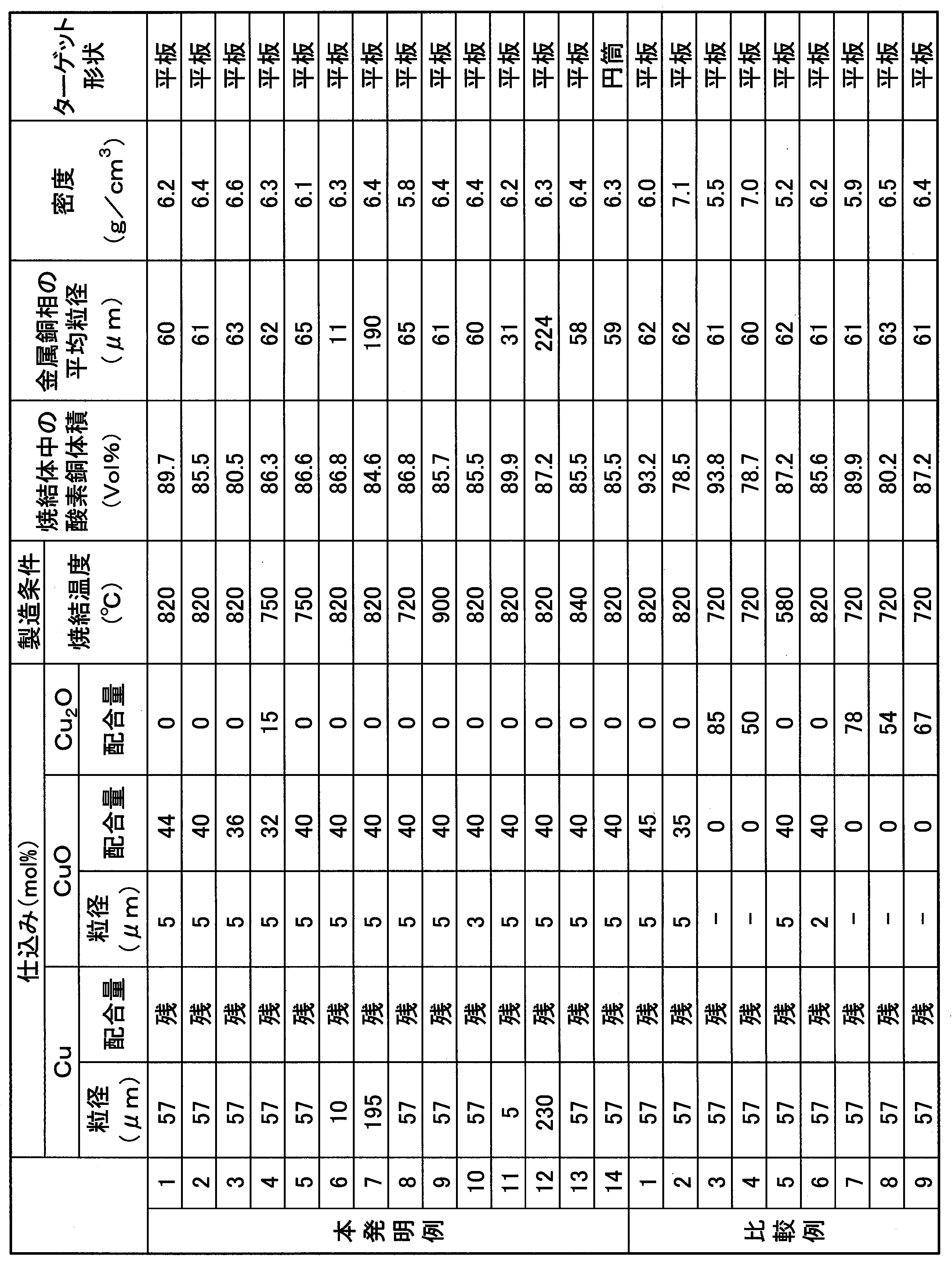
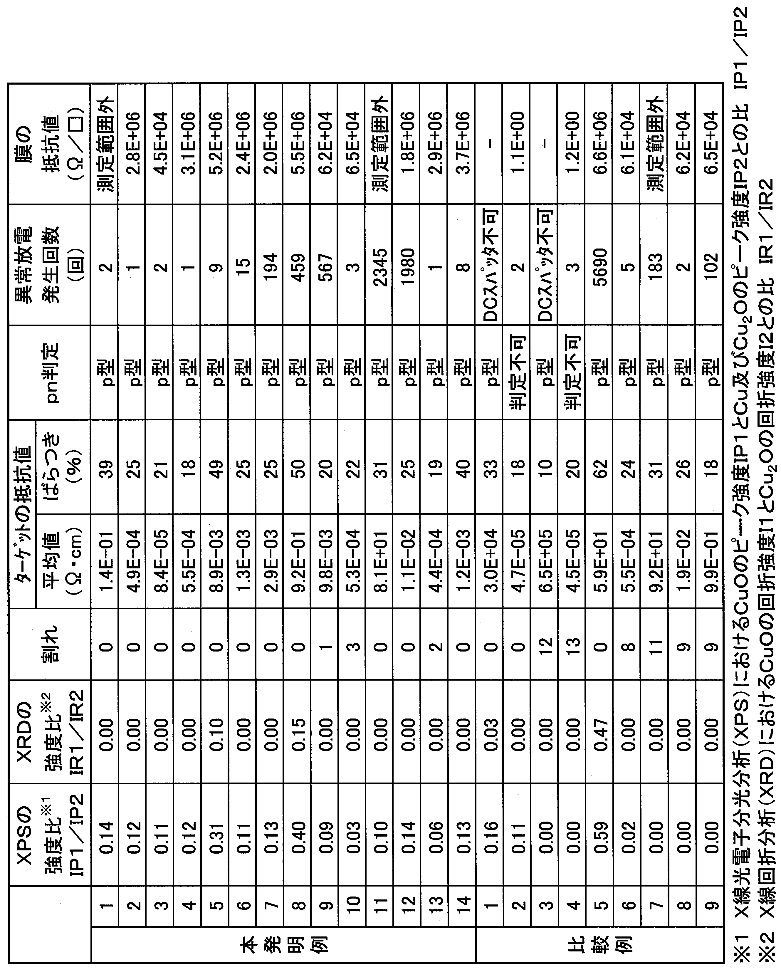
酸化銅相の体積率が90vol%を超えた比較例1及び比較例3においては、抵抗値が高く、DCスパッタができなかった。
酸化銅相の体積率が80vol%以下とされた比較例2及び比較例4においては、成膜された酸化銅膜の抵抗値が低く、酸化銅膜としての特性が不十分であった。
酸化銅相の体積率が80vol%以下とされた比較例2及び比較例4においては、成膜された酸化銅膜の抵抗値が低く、酸化銅膜としての特性が不十分であった。
また、X線光電子分光分析の結果、CuOのピーク強度IP1とCu及びCu2Oのピーク強度IP2との比IP1/IP2が0.03未満とされた比較例3,4,6-9においては、製造時における割れの発生回数が多かった。なお、比較例3,4、7-9では、原料としてCuO粉を用いていないため、IP1/IP2が0であった。また、比較例6においては、CuO粉の平均粒径が2μmと小さいため、CuOが十分に残存せず、IP1/IP2が0.02であった。
さらに、CuOのピーク強度IP1とCu及びCu2Oのピーク強度IP2との比IP1/IP2が0.4を超える比較例5においては、抵抗値のばらつきが大きくなった。また、異常放電の発生回数が多く、安定してDCスパッタすることができなかった。この比較例5においては、焼結工程における焼結温度が580℃と低いため、CuとCuOとの反応が不十分であったためと推測される。
これに対して、X線光電子分光分析の結果、CuOのピーク強度IP1とCu及びCu2Oのピーク強度IP2との比IP1/IP2が0.03以上0.4以下の範囲内とされた本発明例1-14によれば、製造時の割れの発生が抑制されていることが確認された。また、抵抗値が低く、DCスパッタが可能であり、特性に優れた酸化銅膜を成膜可能であることが確認された。
Claims (3)
- 金属銅相と酸化銅相とを有し、前記酸化銅相の体積率が80vol%を超えて90vol%以下の範囲内とされており、
X線光電子分光分析の結果、CuOのピーク強度IP1とCu及びCu2Oのピーク強度IP2との比IP1/IP2が、0.03以上0.4以下の範囲内とされていることを特徴とするスパッタリングターゲット。 - X線回折分析の結果、CuOの回折強度IR1とCu2Oの回折強度IR2との比IR1/IR2が0.15以下であることを特徴とする請求項1に記載のスパッタリングターゲット。
- 金属銅相と酸化銅相とを有し、前記酸化銅相の体積率が80vol%を超えて90vol%以下の範囲内とされたスパッタリングターゲットの製造方法であって、
少なくともCu粉とCuO粉とを含有する原料粉を準備する原料粉準備工程と、前記原料粉を焼結して焼結体を得る焼結工程と、を備えており、
前記CuO粉の平均粒径を3μm以上とし、焼結温度を720℃以上とすることを特徴とするスパッタリングターゲットの製造方法。
Priority Applications (1)
| Application Number | Priority Date | Filing Date | Title |
|---|---|---|---|
| KR1020197019671A KR102302021B1 (ko) | 2017-03-01 | 2018-03-01 | 스퍼터링 타깃 및 스퍼터링 타깃의 제조 방법 |
Applications Claiming Priority (4)
| Application Number | Priority Date | Filing Date | Title |
|---|---|---|---|
| JP2017-038578 | 2017-03-01 | ||
| JP2017038578 | 2017-03-01 | ||
| JP2018024510A JP6447761B2 (ja) | 2017-03-01 | 2018-02-14 | スパッタリングターゲット及びスパッタリングターゲットの製造方法 |
| JP2018-024510 | 2018-02-14 |
Publications (1)
| Publication Number | Publication Date |
|---|---|
| WO2018159753A1 true WO2018159753A1 (ja) | 2018-09-07 |
Family
ID=63370434
Family Applications (1)
| Application Number | Title | Priority Date | Filing Date |
|---|---|---|---|
| PCT/JP2018/007754 Ceased WO2018159753A1 (ja) | 2017-03-01 | 2018-03-01 | スパッタリングターゲット及びスパッタリングターゲットの製造方法 |
Country Status (1)
| Country | Link |
|---|---|
| WO (1) | WO2018159753A1 (ja) |
Citations (4)
| Publication number | Priority date | Publication date | Assignee | Title |
|---|---|---|---|---|
| JP2008280545A (ja) * | 2007-05-08 | 2008-11-20 | Mitsubishi Materials Corp | 酸素含有銅ターゲット |
| JP2011084754A (ja) * | 2009-10-13 | 2011-04-28 | Hitachi Metals Ltd | スパッタリングターゲットの製造方法 |
| WO2015170534A1 (ja) * | 2014-05-08 | 2015-11-12 | 三井金属鉱業株式会社 | スパッタリングターゲット材 |
| JP2017172039A (ja) * | 2016-03-22 | 2017-09-28 | 三菱マテリアル株式会社 | スパッタリングターゲット |
-
2018
- 2018-03-01 WO PCT/JP2018/007754 patent/WO2018159753A1/ja not_active Ceased
Patent Citations (4)
| Publication number | Priority date | Publication date | Assignee | Title |
|---|---|---|---|---|
| JP2008280545A (ja) * | 2007-05-08 | 2008-11-20 | Mitsubishi Materials Corp | 酸素含有銅ターゲット |
| JP2011084754A (ja) * | 2009-10-13 | 2011-04-28 | Hitachi Metals Ltd | スパッタリングターゲットの製造方法 |
| WO2015170534A1 (ja) * | 2014-05-08 | 2015-11-12 | 三井金属鉱業株式会社 | スパッタリングターゲット材 |
| JP2017172039A (ja) * | 2016-03-22 | 2017-09-28 | 三菱マテリアル株式会社 | スパッタリングターゲット |
Similar Documents
| Publication | Publication Date | Title |
|---|---|---|
| JP6876268B2 (ja) | スパッタリングターゲット | |
| JP5808513B1 (ja) | スパッタリングターゲット材 | |
| TWI488826B (zh) | An indium oxide sintered body, an indium oxide transparent conductive film, and a method for producing the transparent conductive film | |
| JP5624977B2 (ja) | 鉛フリー抵抗体組成物 | |
| US20170178876A1 (en) | Cu-Ga ALLOY SPUTTERING TARGET AND METHOD FOR MANUFACTURING SAME | |
| TWI554627B (zh) | Sputtering target and high resistance transparent film manufacturing method | |
| TW201118058A (en) | Indium oxide sintered body and indium oxide transparent conductive film | |
| JP6447761B2 (ja) | スパッタリングターゲット及びスパッタリングターゲットの製造方法 | |
| JP2017025348A (ja) | Mo−W酸化物スパッタリングターゲット、及び、Mo−W酸化物スパッタリングターゲットの製造方法 | |
| TWI572722B (zh) | W-Ti濺鍍靶 | |
| WO2014122120A1 (en) | (ga) zn sn oxide sputtering target | |
| WO2018159753A1 (ja) | スパッタリングターゲット及びスパッタリングターゲットの製造方法 | |
| JP6233233B2 (ja) | スパッタリングターゲット及びその製造方法 | |
| WO2017164168A1 (ja) | スパッタリングターゲット | |
| JPWO2006095733A1 (ja) | 非晶質透明導電膜、ターゲット及び非晶質透明導電膜の製造方法 | |
| WO2003082769A1 (en) | Silicon monoxide sintered product and sputtering target comprising the same | |
| Pogodin et al. | Microstructural, mechanical properties and electrical conductivity of Ag7 (Si1-xGex) S5I-based ceramics | |
| JP7711462B2 (ja) | 抵抗体の製造方法 | |
| JP7711439B2 (ja) | 抵抗体の製造方法 | |
| JP7711440B2 (ja) | 抵抗体の製造方法 | |
| TWI837462B (zh) | Cu-W-O濺鍍靶及氧化物薄膜 | |
| TWI789698B (zh) | 氧化銅糊料及電子零件之製造方法 | |
| JP2020007627A (ja) | スパッタリングターゲットの製造方法 | |
| JP2015074789A (ja) | 酸化ニオブ系スパッタリングターゲット及びその製造方法 | |
| JP2017171986A (ja) | スパッタリングターゲットおよびその製造方法 |
Legal Events
| Date | Code | Title | Description |
|---|---|---|---|
| 121 | Ep: the epo has been informed by wipo that ep was designated in this application |
Ref document number: 18761365 Country of ref document: EP Kind code of ref document: A1 |
|
| ENP | Entry into the national phase |
Ref document number: 20197019671 Country of ref document: KR Kind code of ref document: A |
|
| NENP | Non-entry into the national phase |
Ref country code: DE |
|
| 122 | Ep: pct application non-entry in european phase |
Ref document number: 18761365 Country of ref document: EP Kind code of ref document: A1 |