WO2018154874A1 - シリコン単結晶の製造方法、整流部材、および、単結晶引き上げ装置 - Google Patents
シリコン単結晶の製造方法、整流部材、および、単結晶引き上げ装置 Download PDFInfo
- Publication number
- WO2018154874A1 WO2018154874A1 PCT/JP2017/040890 JP2017040890W WO2018154874A1 WO 2018154874 A1 WO2018154874 A1 WO 2018154874A1 JP 2017040890 W JP2017040890 W JP 2017040890W WO 2018154874 A1 WO2018154874 A1 WO 2018154874A1
- Authority
- WO
- WIPO (PCT)
- Prior art keywords
- single crystal
- silicon single
- crucible
- dopant
- rectifying member
- Prior art date
- Legal status (The legal status is an assumption and is not a legal conclusion. Google has not performed a legal analysis and makes no representation as to the accuracy of the status listed.)
- Ceased
Links
Images




Classifications
-
- H—ELECTRICITY
- H10—SEMICONDUCTOR DEVICES; ELECTRIC SOLID-STATE DEVICES NOT OTHERWISE PROVIDED FOR
- H10P—GENERIC PROCESSES OR APPARATUS FOR THE MANUFACTURE OR TREATMENT OF DEVICES COVERED BY CLASS H10
- H10P14/00—Formation of materials, e.g. in the shape of layers or pillars
- H10P14/20—Formation of materials, e.g. in the shape of layers or pillars of semiconductor materials
- H10P14/27—Formation of materials, e.g. in the shape of layers or pillars of semiconductor materials using selective deposition, e.g. simultaneous growth of monocrystalline and non-monocrystalline semiconductor materials
-
- C—CHEMISTRY; METALLURGY
- C30—CRYSTAL GROWTH
- C30B—SINGLE-CRYSTAL GROWTH; UNIDIRECTIONAL SOLIDIFICATION OF EUTECTIC MATERIAL OR UNIDIRECTIONAL DEMIXING OF EUTECTOID MATERIAL; REFINING BY ZONE-MELTING OF MATERIAL; PRODUCTION OF A HOMOGENEOUS POLYCRYSTALLINE MATERIAL WITH DEFINED STRUCTURE; SINGLE CRYSTALS OR HOMOGENEOUS POLYCRYSTALLINE MATERIAL WITH DEFINED STRUCTURE; AFTER-TREATMENT OF SINGLE CRYSTALS OR A HOMOGENEOUS POLYCRYSTALLINE MATERIAL WITH DEFINED STRUCTURE; APPARATUS THEREFOR
- C30B15/00—Single-crystal growth by pulling from a melt, e.g. Czochralski method
- C30B15/14—Heating of the melt or the crystallised materials
-
- C—CHEMISTRY; METALLURGY
- C30—CRYSTAL GROWTH
- C30B—SINGLE-CRYSTAL GROWTH; UNIDIRECTIONAL SOLIDIFICATION OF EUTECTIC MATERIAL OR UNIDIRECTIONAL DEMIXING OF EUTECTOID MATERIAL; REFINING BY ZONE-MELTING OF MATERIAL; PRODUCTION OF A HOMOGENEOUS POLYCRYSTALLINE MATERIAL WITH DEFINED STRUCTURE; SINGLE CRYSTALS OR HOMOGENEOUS POLYCRYSTALLINE MATERIAL WITH DEFINED STRUCTURE; AFTER-TREATMENT OF SINGLE CRYSTALS OR A HOMOGENEOUS POLYCRYSTALLINE MATERIAL WITH DEFINED STRUCTURE; APPARATUS THEREFOR
- C30B15/00—Single-crystal growth by pulling from a melt, e.g. Czochralski method
- C30B15/20—Controlling or regulating
-
- C—CHEMISTRY; METALLURGY
- C30—CRYSTAL GROWTH
- C30B—SINGLE-CRYSTAL GROWTH; UNIDIRECTIONAL SOLIDIFICATION OF EUTECTIC MATERIAL OR UNIDIRECTIONAL DEMIXING OF EUTECTOID MATERIAL; REFINING BY ZONE-MELTING OF MATERIAL; PRODUCTION OF A HOMOGENEOUS POLYCRYSTALLINE MATERIAL WITH DEFINED STRUCTURE; SINGLE CRYSTALS OR HOMOGENEOUS POLYCRYSTALLINE MATERIAL WITH DEFINED STRUCTURE; AFTER-TREATMENT OF SINGLE CRYSTALS OR A HOMOGENEOUS POLYCRYSTALLINE MATERIAL WITH DEFINED STRUCTURE; APPARATUS THEREFOR
- C30B15/00—Single-crystal growth by pulling from a melt, e.g. Czochralski method
- C30B15/10—Crucibles or containers for supporting the melt
-
- C—CHEMISTRY; METALLURGY
- C30—CRYSTAL GROWTH
- C30B—SINGLE-CRYSTAL GROWTH; UNIDIRECTIONAL SOLIDIFICATION OF EUTECTIC MATERIAL OR UNIDIRECTIONAL DEMIXING OF EUTECTOID MATERIAL; REFINING BY ZONE-MELTING OF MATERIAL; PRODUCTION OF A HOMOGENEOUS POLYCRYSTALLINE MATERIAL WITH DEFINED STRUCTURE; SINGLE CRYSTALS OR HOMOGENEOUS POLYCRYSTALLINE MATERIAL WITH DEFINED STRUCTURE; AFTER-TREATMENT OF SINGLE CRYSTALS OR A HOMOGENEOUS POLYCRYSTALLINE MATERIAL WITH DEFINED STRUCTURE; APPARATUS THEREFOR
- C30B27/00—Single-crystal growth under a protective fluid
- C30B27/02—Single-crystal growth under a protective fluid by pulling from a melt
-
- C—CHEMISTRY; METALLURGY
- C30—CRYSTAL GROWTH
- C30B—SINGLE-CRYSTAL GROWTH; UNIDIRECTIONAL SOLIDIFICATION OF EUTECTIC MATERIAL OR UNIDIRECTIONAL DEMIXING OF EUTECTOID MATERIAL; REFINING BY ZONE-MELTING OF MATERIAL; PRODUCTION OF A HOMOGENEOUS POLYCRYSTALLINE MATERIAL WITH DEFINED STRUCTURE; SINGLE CRYSTALS OR HOMOGENEOUS POLYCRYSTALLINE MATERIAL WITH DEFINED STRUCTURE; AFTER-TREATMENT OF SINGLE CRYSTALS OR A HOMOGENEOUS POLYCRYSTALLINE MATERIAL WITH DEFINED STRUCTURE; APPARATUS THEREFOR
- C30B29/00—Single crystals or homogeneous polycrystalline material with defined structure characterised by the material or by their shape
- C30B29/02—Elements
- C30B29/06—Silicon
-
- H—ELECTRICITY
- H10—SEMICONDUCTOR DEVICES; ELECTRIC SOLID-STATE DEVICES NOT OTHERWISE PROVIDED FOR
- H10P—GENERIC PROCESSES OR APPARATUS FOR THE MANUFACTURE OR TREATMENT OF DEVICES COVERED BY CLASS H10
- H10P14/00—Formation of materials, e.g. in the shape of layers or pillars
- H10P14/20—Formation of materials, e.g. in the shape of layers or pillars of semiconductor materials
- H10P14/29—Formation of materials, e.g. in the shape of layers or pillars of semiconductor materials characterised by the substrates
- H10P14/2901—Materials
- H10P14/2902—Materials being Group IVA materials
- H10P14/2905—Silicon, silicon germanium or germanium
-
- H—ELECTRICITY
- H10—SEMICONDUCTOR DEVICES; ELECTRIC SOLID-STATE DEVICES NOT OTHERWISE PROVIDED FOR
- H10P—GENERIC PROCESSES OR APPARATUS FOR THE MANUFACTURE OR TREATMENT OF DEVICES COVERED BY CLASS H10
- H10P14/00—Formation of materials, e.g. in the shape of layers or pillars
- H10P14/20—Formation of materials, e.g. in the shape of layers or pillars of semiconductor materials
- H10P14/32—Formation of materials, e.g. in the shape of layers or pillars of semiconductor materials characterised by intermediate layers between substrates and deposited layers
- H10P14/3242—Structure
- H10P14/3256—Microstructure
-
- H—ELECTRICITY
- H10—SEMICONDUCTOR DEVICES; ELECTRIC SOLID-STATE DEVICES NOT OTHERWISE PROVIDED FOR
- H10P—GENERIC PROCESSES OR APPARATUS FOR THE MANUFACTURE OR TREATMENT OF DEVICES COVERED BY CLASS H10
- H10P14/00—Formation of materials, e.g. in the shape of layers or pillars
- H10P14/20—Formation of materials, e.g. in the shape of layers or pillars of semiconductor materials
- H10P14/34—Deposited materials, e.g. layers
- H10P14/3451—Structure
- H10P14/3452—Microstructure
- H10P14/3458—Monocrystalline
Definitions
- the present invention relates to a method for producing a silicon single crystal, a rectifying member, and a single crystal pulling apparatus.
- Patent Document 1 Conventionally, a method of manufacturing a silicon single crystal using a Czochralski (CZ) method is known (for example, see Patent Document 1).
- the single crystal pulling device of Patent Document 1 includes a tubular body that coaxially surrounds a silicon single crystal, and a gas rectifying member that is provided at the lower end of the tubular body and has a truncated conical surface that extends downward. .
- An opening is provided in the vicinity of the coupling portion between the tubular body and the gas rectifying member.
- the inner diameter of the gas rectifying member is smaller than the inner diameter of the tubular body.
- Patent Document 1 is not sufficient in reducing the dopant evaporation.
- An object of the present invention is to provide a method for producing a silicon single crystal, a rectifying member, and a single crystal pulling apparatus capable of reducing evaporation of dopant.
- the method for producing a silicon single crystal of the present invention includes a crucible, a crucible driving unit that moves the crucible up and down, and a heating unit that heats the crucible and generates a dopant-added melt in which a dopant is added to a silicon melt.
- a single crystal pulling apparatus including a body, a chamber for housing the crucible, the heating unit, and the heat shield, and an introduction unit provided at an upper portion of the chamber for introducing an inert gas into the chamber.
- a method for producing a silicon single crystal comprising: a rectifying member including an annular plate-shaped main body surrounding the silicon single crystal below the thermal shield; During the growth of the recon single crystal, the pressure inside the chamber is controlled to 20 kPa or more, and while maintaining the state where the rectifying member is separated from the dopant-added melt, the silicon single crystal and the thermal shield.
- the inert gas is introduced from above, and the inert gas is separated from the silicon single crystal along the first flow path between the thermal shield and the rectifying member; and It separates into the 2nd distribution gas which separates from the silicon single crystal along the 2nd channel between the baffle member and the dopant addition melt surface.
- the present invention by controlling the pressure inside the chamber to 20 kPa or higher and higher than the conventional pressure, the partial pressure of the dopant volatilized inside the chamber is lowered, and evaporation of the dopant from the dopant-added melt surface can be reduced. Further, by separating the inert gas into a first flow gas flowing between the heat shield and the flow straightening member and a second flow gas flowing between the flow straightening member and the dopant-added melt surface by the flow straightening member, Since the flow rate of the second flow gas decreases, the evaporation of the dopant from the dopant-added melt surface can be reduced.
- the rectifying member having an inner diameter of the main body portion smaller than an inner diameter of the lower end of the thermal shield is disposed, and the inner side of the lower end of the thermal shield in the main body is disposed.
- Forming a gas receiving portion positioned, and introducing the inert gas into the first flow path along the upper surface of the gas receiving portion; and the silicon single crystal side from the gas receiving portion. It is preferable to separate into the second circulation gas that passes through and is guided to the second flow path.
- the flow rate of the first circulation gas can be increased by forming the gas receiving portion located inside the lower end of the heat shield in the main body portion.
- the flow rate of the second flow gas decreases, it is possible to further reduce the evaporation of the dopant from the dopant-added melt surface.
- the method for producing a silicon single crystal of the present invention it is preferable to grow the silicon single crystal while maintaining a state in which the height of the first flow path is higher than the height of the second flow path.
- the flow rate of the first circulation gas can be increased by maintaining the state where the height of the first flow path is higher than the height of the second flow path.
- the flow rate of the second flow gas decreases, it is possible to further reduce the evaporation of the dopant from the dopant-added melt surface.
- the rectifying member including an extending portion extending obliquely upward and outward from an outer edge of the main body portion is disposed, and the first flow gas is guided obliquely upward and outward. Is preferred.
- the first flow gas can be moved away from the vicinity of the dopant-added melt surface at the extending portion, and the inert gas flowing on the dopant-added melt surface can be reduced.
- the evaporation of the dopant from the surface of the dopant-added melt can be further reduced.
- the outside of the straightening member is bent upward, even if the growth of the silicon single crystal progresses and the dopant-added melt decreases, the outside extension of the straightening member is rounded. The pulling can be continued without contacting the inner surface of the bottom-shaped crucible whose diameter is reduced toward the bottom, such as the bottom.
- the rectifying member is disposed so that an upper end of the extension portion is located above a lower end of the thermal shield, and the dopant-added melt, the crucible, and the crucible It is preferable that the extending portion suppresses radiant heat from at least one of the heating portions from reaching the silicon single crystal via the first flow path.
- the radiant heat from at least one of the dopant-added melt, the crucible, and the heating portion is reduced by the lower end of the heat shield. And reaching the silicon single crystal through the first flow path between the main body portion of the rectifying member. As a result, the temperature gradient in the pulling direction of the silicon single crystal can be increased.
- the rectifying member having a heat insulating material provided therein is disposed, and radiant heat from at least one of the dopant-added melt, the crucible, and the heating unit is generated by the silicon. It is preferable to suppress the single crystal from reaching the single crystal.
- the present invention by providing a heat insulating material inside the rectifying member, it is possible to effectively suppress radiation heat from at least one of the dopant-added melt, the crucible, and the heating unit from reaching the silicon single crystal. can do.
- the rectifying member of the present invention includes a crucible, a crucible driving unit that raises and lowers and rotates the crucible, a heating unit that heats the crucible and generates a dopant-added melt in which a dopant is added to a silicon melt, and a seed crystal Is pulled after contacting the dopant-added melt, a pulling portion for growing a silicon single crystal, a cylindrical heat shield provided so as to surround the silicon single crystal above the crucible, A rectifying member attached to a single crystal pulling apparatus provided with a crucible, a chamber containing the heating unit and the thermal shield, and an introduction unit provided at an upper portion of the chamber for introducing an inert gas into the chamber.
- a body portion forming a second flow path between the dopant addition the melt surface, characterized in that it comprises a extending portion which extends obliquely upwardly outwardly from an outer edge of the main body portion.
- a heat insulating material is provided in at least one of the main body portion and the extending portion.
- the single crystal pulling apparatus of the present invention includes a crucible, a crucible driving unit that raises and lowers and rotates the crucible, a heating unit that heats the crucible and generates a dopant-added melt in which a dopant is added to a silicon melt, A pulling part for growing a silicon single crystal by pulling the seed crystal after bringing it into contact with the dopant-added melt, and a cylindrical heat shield provided so as to surround the silicon single crystal above the crucible
- the crucible, the heating unit and the chamber for housing the thermal shield, the upper part of the chamber, an introduction part for introducing an inert gas into the chamber, and the thermal shield are provided below the thermal shield It has the above-mentioned rectifying member.
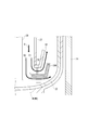
- Sectional drawing of the single crystal pulling apparatus which concerns on one Embodiment of this invention.
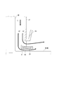
- Explanatory drawing which shows the flow of the inert gas of the dopant addition melt surface vicinity in case a rectification
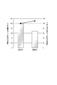
- the graph which shows the relationship between the presence or absence of the rectification
- the single crystal pulling apparatus 1 includes a chamber 21, a crucible 22 disposed inside the chamber 21, a crucible driving unit 23, a heating unit 24, a heat insulating cylinder 25, a pulling unit 26, The rectifying cylinder 27, the heat shield 28, and the rectifying member 29 are provided.
- an introduction part 21 ⁇ / b> A for introducing an inert gas such as Ar gas into the chamber 21 is provided in the upper part of the chamber 21.
- An exhaust port 21 ⁇ / b> B that exhausts gas inside the chamber 21 by driving a vacuum pump (not shown) is provided at the lower portion of the chamber 21.
- An inert gas is introduced into the chamber 21 from the introduction portion 21A in a predetermined gas amount.
- the introduced inert gas is discharged from the exhaust port 21 ⁇ / b> B at the lower part of the chamber 21, so that the inert gas flows downward from the inside of the chamber 21.
- the crucible 22 melts polycrystalline silicon, which is a raw material of the silicon single crystal SM, to form a silicon melt M.
- the crucible drive unit 23 moves the crucible 22 up and down at a predetermined speed, and rotates the crucible 22 at a predetermined speed around a support shaft 23 ⁇ / b> A connected to the lower end of the crucible 22.
- the heating unit 24 is disposed outside the crucible 22, and heats the crucible 22 to generate a dopant-added melt MD in which a dopant is added to the silicon melt M.
- the heat insulating cylinder 25 is disposed so as to surround the crucible 22 and the heating unit 24.
- the pulling unit 26 includes a pulling drive unit 26A and a pulling cable 26B having one end connected to the pulling drive unit 26A.
- the pulling drive unit 26A moves the pulling cable 26B up and down and rotates at a predetermined speed.
- a seed holder 26C for holding a seed crystal or a doping device (not shown) is attached.
- the doping apparatus is for doping the silicon melt M in the crucible 22 with the dopant to generate the dopant-added melt MD.
- the rectifying cylinder 27 is provided in a cylindrical shape surrounding the silicon single crystal SM, and guides an inert gas flowing from above to below.
- the heat shield 28 is formed in the shape of a truncated cone surrounding the lower part of the rectifying cylinder 27 and the silicon single crystal SM above the crucible 22, and the lower end thereof is connected to the lower end of the rectifying cylinder 27.
- the heat shield 28 blocks radiant heat radiated upward from the heating unit 24.
- the rectifying member 29 includes a main body portion 29A formed in an annular plate shape, an extending portion 29B extending obliquely upward and outward from the outer edge of the main body portion 29A, and a protruding portion 29C protruding upward from the inner edge of the main body portion 29A. And.
- the inner diameter D2 of the main body 29A is smaller than the inner diameter D1 of the lower end of the heat shield 28.
- a heat insulating material 29D is provided inside the main body 29A and the extension 29B.
- the rectifying member 29 is disposed below the heat shield 28 via the support member 30 and so as to surround the silicon single crystal SM.
- the support member 30 has a rod-like shape, and connects the heat shield 28 and the rectifying member 29 at two to four positions so as to be substantially equidistant in the circumferential direction of the silicon single crystal SM.
- an annular gas receiving portion 29 ⁇ / b> E is formed inside the lower end of the heat shield 28.
- the gas receiving portion 29E is a part of the inner region of the main body portion 29A, and extends from the inner peripheral surface of the main body portion 29A and the extension line of the inner surface of the rectifying cylinder 27 indicated by the dotted line in FIG. The region up to the intersection with the upper surface of the portion 29A.
- the upper surface of the main body portion 29A of the rectifying member 29 and the upper surface of the extending portion 29B are arranged so as to be parallel to the bottom surface 28A of the heat shield 28 and the outer peripheral side surface 28B of the heat shield 28, respectively. Between these, the 1st flow path R1 is formed. In addition, a second flow path R2 is formed between the rectifying member 29 and the dopant-added melt MD surface. Further, the rectifying member 29 is disposed so that the upper end of the extending portion 29 ⁇ / b> B is located above the bottom surface 28 ⁇ / b> A of the heat shield 28.
- silicon single crystal SM having a set diameter of the straight body portion of 200 mm is illustrated, but silicon single crystals SM having other set diameters such as 150 mm, 300 mm, and 450 mm may be manufactured.
- the electrical resistivity is preferably 1.2 m ⁇ ⁇ cm to 5.0 m ⁇ ⁇ cm when the dopant is arsenic, and 0.5 m ⁇ ⁇ cm to 2.0 m ⁇ ⁇ cm when red phosphorus is used.
- antimony it is preferably 10 m ⁇ ⁇ cm or more and 30 m ⁇ ⁇ cm or less.
- the inert gas flow rate, the pressure inside the chamber 21, the crucible 22, The rotational speed of the silicon single crystal SM, the heating conditions of the heating unit 24, and the like are set.
- the heating unit 24 is controlled based on the set value, and the crucible 22 is heated, so that polycrystalline silicon (silicon raw material) and the dopant in the crucible 22 are melted to generate a dopant-added melt MD.
- an inert gas is introduced into the chamber 21 from the introduction portion 21A at a predetermined flow rate, and the pressure inside the chamber 21 is maintained at 20 kPa or more.
- the pressure inside the chamber 21 is preferably 80 kPa or less.
- the pulling cable 26B is lowered to immerse the seed crystal in the dopant-added melt MD, and the silicon single crystal SM is pulled and grown while rotating the crucible 22 and the pulling cable 26B in a predetermined direction.
- the inert gas G flowing downward is separated into the first flow gas G ⁇ b> 1 and the second flow gas G ⁇ b> 2 by the rectifying member 29.
- the inert gas G is guided to the first flow path R1 by the gas receiving portion 29E, and the flow rate of the first flow gas G1 increases, so that the flow rate of the second flow gas G2 can be decreased.
- evaporation of the dopant can be reduced by setting the pressure inside the chamber 21 to 20 kPa or higher, which is higher than the conventional pressure, lowering the partial pressure of the dopant, and reducing the flow rate of the second flow gas G2.
- the crucible 22 has a height H1 of the first flow path R1 that is maintained higher than a height H2 of the second flow path R2 in accordance with the speed at which the liquid level of the dopant-added melt MD decreases.
- the ascent rate is controlled. Therefore, the flow rate of the first flow gas G1 can be increased and the flow rate of the second flow gas G2 can be decreased.
- the first flowing gas G1 is further guided obliquely upward and outward by the extending portion 29B, and hardly flows into the dopant added melt MD surface vicinity region P surrounded by the dotted line in FIG. For this reason, evaporation of the dopant can be reduced.
- a silicon single crystal SM having a desired electrical resistivity can be manufactured by suppressing the evaporation of the dopant.
- the rectifying member 29 since the outer side of the rectifying member 29 is bent upward, as shown in FIG. 3, even if the growth of the silicon single crystal SM progresses and the dopant-added melt MD decreases, the rectification is performed.
- the extending portion 29B outside the member 29 can continue to be pulled up without contacting the inner surface of the bottom-shaped crucible 22 whose diameter is reduced toward the bottom, such as a round bottom.
- the radiant heat from at least one of the dopant-added melt MD, the crucible 22 and the heating part 24 is the first. Reaching the silicon single crystal SM via the flow path R1 can be suppressed by the extending portion 29B, and the temperature gradient in the pulling direction of the silicon single crystal SM can be increased. Furthermore, since the radiant heat can be more effectively insulated by the heat insulating material 29D inside the rectifying member 29, the temperature gradient in the pulling direction of the silicon single crystal SM can be further increased.
- the present invention is not limited to the above-described embodiment, and various improvements and design changes can be made without departing from the scope of the present invention.
- the general procedure, structure, and the like may be other structures as long as the object of the present invention can be achieved.
- the silicon single crystal SM can be manufactured by reducing the evaporation of the dopant as in the above embodiment.
- the inner diameter D2 of the main body portion 29A may be the same as the inner diameter D1 at the lower end of the heat shield 28 or may be larger than the inner diameter D1.
- the height H1 of the first flow path R1 may be the same as the height H2 of the second flow path R2, or may be lower than the height H2. Furthermore, as illustrated in FIG. 4, the extending portion 29 ⁇ / b> B may not be provided in the rectifying member 29. Even when the extending portion 29B is provided, the main body portion 29A and the extending portion 29B may not be provided so as to be parallel to the bottom surface 28A of the heat shield 28 and the outer peripheral side surface 28B of the heat shield 28.
- the upper end of the protruding portion 29B may be the same height as the lower end of the heat shield 28 or lower than the lower end of the heat shield 28, or the heat insulating material 29D may not be provided inside.
- the dopant concentration taken into the silicon single crystal SM was calculated, and the amount of evaporation from the dopant-added melt MD was calculated based on the taken-in dopant concentration.
- the amount of evaporation calculated in this way increases as the electrical resistivity of the silicon single crystal SM increases with respect to a desired value.
- Example 2 A single crystal pulling apparatus 1 provided with a rectifying member 29 as shown in FIG. 1 in the single crystal pulling apparatus used in Experimental Example 1 was prepared.
- the configuration of each part of the single crystal pulling apparatus 1 was set as follows. ⁇ Configuration of each part of single crystal pulling device> Inner diameter D2 of main body 29A of rectifying member 29: 250 mm First flow path R1 height H1: 10 mm Gas receiving part 29E width: 15 mm
- FIG. 5 shows the dopant evaporation amount ratio of Experimental Examples 2 to 5 when the dopant evaporation amount of Experimental Example 1 is 100%. Comparing Experimental Example 1 and Experimental Example 2, it was found that the amount of evaporation of the dopant can be reduced by providing the rectifying member 29, but the amount of decrease is not sufficient. Comparing Experimental Examples 2 to 5, in Experimental Example 3, the amount of dopant evaporation can be greatly reduced compared to Experimental Example 2. From the results of Experimental Examples 4 and 5, the amount of dopant evaporation increases as the pressure inside the chamber 21 increases. It was found that can be greatly reduced.
- Example 2 Investigation of the relationship between the presence or absence of rectifying members and electrical resistivity
- a silicon single crystal was manufactured under the same conditions as in Experimental Example 1 and Experimental Example 5, and the electrical resistivity of each solidification rate in the straight body portion was measured.
- FIG. 6 shows the measurement results.
- the upper end of a straight body part is a solidification rate 0%, and a lower end is 100%.
- the dopant evaporation amount of Experimental Example 5 was reduced to about 70% of Experimental Example 6. From this, it was found that by providing the extending portion 29B on the rectifying member 29, the first flow gas G1 can be guided obliquely upward and outward, and evaporation of the dopant can be reduced. Further, the temperature gradient of Experimental Example 5 increased to about 110% of Experimental Example 6. From this, by providing the extension part 29B in the rectifying member 29, the radiant heat from at least one of the dopant-added melt MD, the crucible 22 and the heating part 24 is transmitted through the first flow path R1 to the silicon single crystal. It was found that it can be suppressed to reach.
Landscapes
- Chemical & Material Sciences (AREA)
- Crystallography & Structural Chemistry (AREA)
- Engineering & Computer Science (AREA)
- Materials Engineering (AREA)
- Metallurgy (AREA)
- Organic Chemistry (AREA)
- Crystals, And After-Treatments Of Crystals (AREA)
Abstract
シリコン単結晶の製造方法は、熱遮蔽体(28)の下方においてシリコン単結晶(SM)を囲む円環板状の本体部(29A)を備えた整流部材を配置し、シリコン単結晶(SM)の育成中に、チャンバ内部の圧力を20kPa以上に制御し、整流部材をドーパント添加融液(MD)から離間させた状態を維持し、シリコン単結晶(SM)と熱遮蔽体(28)との間に不活性ガス(G)を導入し、不活性ガス(G)を第1流通ガス(G1)と、第2流通ガス(G2)とに分離する。
Description
本発明は、シリコン単結晶の製造方法、整流部材、および、単結晶引き上げ装置に関する。
従来、チョクラルスキー(CZ)法を利用して、シリコン単結晶を製造する方法が知られている(例えば、特許文献1参照)。
特許文献1の単結晶引き上げ装置は、シリコン単結晶を同軸に包囲する管状体と、この管状体の下端に設けられ、下方に拡がる截頭円錐状の面を有するガス整流部材とを備えている。管状体とガス整流部材の結合部近傍には、開口部が設けられている。ガス整流部材の内径は、管状体の内径より小さくなっている。
アンチモン(Sb)をドーパントとしてシリコン単結晶を製造する際、100mbar(約10kPa)の減圧下において、下方に向かう不活性ガスの大部分を開口部からガス整流部材の截頭円錐状の面に沿って流し、管状体内部を介して溶融体表面の結晶固化部近傍に到達する不活性ガスを少なくすることにより、SiOやSb2O3の蒸発を抑制し、シリコン結晶中の酸素濃度を高くしている。
特許文献1の単結晶引き上げ装置は、シリコン単結晶を同軸に包囲する管状体と、この管状体の下端に設けられ、下方に拡がる截頭円錐状の面を有するガス整流部材とを備えている。管状体とガス整流部材の結合部近傍には、開口部が設けられている。ガス整流部材の内径は、管状体の内径より小さくなっている。
アンチモン(Sb)をドーパントとしてシリコン単結晶を製造する際、100mbar(約10kPa)の減圧下において、下方に向かう不活性ガスの大部分を開口部からガス整流部材の截頭円錐状の面に沿って流し、管状体内部を介して溶融体表面の結晶固化部近傍に到達する不活性ガスを少なくすることにより、SiOやSb2O3の蒸発を抑制し、シリコン結晶中の酸素濃度を高くしている。
しかしながら、特許文献1の方法は、ドーパント蒸発の低減効果は十分なものではなかった。
本発明の目的は、ドーパントの蒸発を低減可能な、シリコン単結晶の製造方法、整流部材、および、単結晶引き上げ装置を提供することにある。
本発明のシリコン単結晶の製造方法は、坩堝と、前記坩堝を昇降および回転させる坩堝駆動部と、前記坩堝を加熱してシリコン融液にドーパントが添加されたドーパント添加融液を生成する加熱部と、種子結晶を前記ドーパント添加融液に接触させた後に引き上げることで、シリコン単結晶を育成する引き上げ部と、前記坩堝の上方において前記シリコン単結晶を囲むように設けられた筒状の熱遮蔽体と、前記坩堝、前記加熱部および前記熱遮蔽体を収容するチャンバと、前記チャンバの上部に設けられ、前記チャンバ内部に不活性ガスを導入する導入部とを備える単結晶引き上げ装置を用いたシリコン単結晶の製造方法であって、前記熱遮蔽体の下方において前記シリコン単結晶を囲む円環板状の本体部を備えた整流部材を配置し、前記シリコン単結晶の育成中に、前記チャンバ内部の圧力を20kPa以上に制御するとともに、前記整流部材を前記ドーパント添加融液から離間させた状態を維持しつつ、前記シリコン単結晶と前記熱遮蔽体との間に上方から前記不活性ガスを導入し、この不活性ガスを前記熱遮蔽体と前記整流部材との間の第1流路に沿って前記シリコン単結晶から離れる第1流通ガスと、前記整流部材と前記ドーパント添加融液表面との間の第2流路に沿って前記シリコン単結晶から離れる第2流通ガスとに分離することを特徴とする。
本発明によれば、チャンバ内部の圧力を20kPa以上と従来よりも高圧に制御することによって、チャンバ内部で揮発するドーパントの分圧が下がり、ドーパント添加融液表面からのドーパントの蒸発を低減できる。また、整流部材により、不活性ガスを、熱遮蔽体と整流部材の間を流れる第1流通ガスと、整流部材とドーパント添加融液表面との間を流れる第2流通ガスに分離したことにより、第2流通ガスの流量が減少するため、ドーパント添加融液表面からのドーパントの蒸発を低減できる。
本発明のシリコン単結晶の製造方法は、前記本体部の内径が前記熱遮蔽体の下端の内径よりも小さい前記整流部材を配置して、前記本体部における前記熱遮蔽体の下端よりも内側に位置するガス受部を形成し、前記不活性ガスを前記ガス受部の上面に沿って前記第1流路に導かれる前記第1流通ガスと、前記ガス受部よりも前記シリコン単結晶側を通過して前記第2流路に導かれる前記第2流通ガスとに分離することが好ましい。
本発明によれば、本体部における熱遮蔽体の下端よりも内側に位置するガス受部を形成することより、第1流通ガスの流量を増加させることができる。その結果、第2流通ガスの流量が減少するため、ドーパント添加融液表面からのドーパントの蒸発をさらに低減できる。
本発明のシリコン単結晶の製造方法は、前記第1流路の高さが前記第2流路の高さよりも高い状態を維持しつつ、前記シリコン単結晶を育成することが好ましい。
本発明によれば、第1流路の高さが第2流路の高さよりも高い状態を維持することにより、第1流通ガスの流量を増加させることができる。その結果、第2流通ガスの流量が減少するため、ドーパント添加融液表面からのドーパントの蒸発をさらに低減できる。
本発明のシリコン単結晶の製造方法は、前記本体部の外縁から斜め上方外側に延出する延出部を備える前記整流部材を配置して、前記第1流通ガスを前記斜め上方外側に導くことが好ましい。
本発明によれば、延出部で第1流通ガスをドーパント添加融液表面近傍から遠ざけることができ、ドーパント添加融液表面を流れる不活性ガスを低減することができる。その結果、ドーパント添加融液表面からのドーパントの蒸発をさらに低減できる。また、整流部材全体としてみた場合、その外側は上方に屈曲しているので、シリコン単結晶の育成が進行してドーパント添加融液が減少しても、整流部材の外側の延出部が、丸底など、底部に向かって縮径した底形状の坩堝の内面に接触することなく引き上げを続行することができる。
本発明のシリコン単結晶の製造方法は、前記延出部の上端が前記熱遮蔽体の下端よりも上側に位置するように前記整流部材を配置して、前記ドーパント添加融液、前記坩堝および前記加熱部のうち少なくとも1つからの輻射熱が、前記第1流路を介して前記シリコン単結晶に到達することを、前記延出部で抑制することが好ましい。
本発明によれば、延出部の上端が熱遮蔽体の下端よりも上側に位置することにより、ドーパント添加融液、坩堝および加熱部のうち少なくとも1つからの輻射熱が、熱遮蔽体の下端と整流部材の本体部の間の第1流路を介して、シリコン単結晶に到達することを抑制できる。その結果、シリコン単結晶の引き上げ方向の温度勾配を大きくすることができる。
本発明のシリコン単結晶の製造方法は、内部に断熱材が設けられた前記整流部材を配置して、前記ドーパント添加融液、前記坩堝および前記加熱部のうち少なくとも1つからの輻射熱が前記シリコン単結晶に到達することを、前記断熱材により抑制することが好ましい。
本発明によれば、整流部材内部に断熱材が設けられていることにより、ドーパント添加融液、坩堝および加熱部のうち少なくとも1つからの輻射熱がシリコン単結晶に到達することを効果的に抑制することができる。
本発明の整流部材は、坩堝と、前記坩堝を昇降および回転させる坩堝駆動部と、前記坩堝を加熱してシリコン融液にドーパントが添加されたドーパント添加融液を生成する加熱部と、種子結晶を前記ドーパント添加融液に接触させた後に引き上げることで、シリコン単結晶を育成する引き上げ部と、前記坩堝の上方において前記シリコン単結晶を囲むように設けられた筒状の熱遮蔽体と、前記坩堝、前記加熱部および前記熱遮蔽体を収容するチャンバと、前記チャンバの上部に設けられ、前記チャンバ内部に不活性ガスを導入する導入部とを備える単結晶引き上げ装置に取り付けられる整流部材であって、前記熱遮蔽体の下方において前記シリコン単結晶を囲む円環板状に形成され、前記熱遮蔽体との間に第1流路を形成するとともに、前記ドーパント添加融液表面との間に第2流路を形成する本体部と、前記本体部の外縁から斜め上方外側に延出する延出部とを備えることを特徴とする。
また、本発明の整流部材は、前記本体部および前記延出部のうち少なくとも一方の内部には、断熱材が設けられていることが好ましい。
本発明の単結晶引き上げ装置は、坩堝と、前記坩堝を昇降および回転させる坩堝駆動部と、前記坩堝を加熱してシリコン融液にドーパントが添加されたドーパント添加融液を生成する加熱部と、種子結晶を前記ドーパント添加融液に接触させた後に引き上げることで、シリコン単結晶を育成する引き上げ部と、前記坩堝の上方において前記シリコン単結晶を囲むように設けられた筒状の熱遮蔽体と、前記坩堝、前記加熱部および前記熱遮蔽体を収容するチャンバと、前記チャンバの上部に設けられ、前記チャンバ内部に不活性ガスを導入する導入部と、前記熱遮蔽体の下方に設けられた上述の整流部材とを備えることを特徴とする。
[実施形態]
以下、本発明の一実施形態として、CZ法によるシリコン単結晶SMの製造方法について図1から図3を参照して説明する。
まず、シリコン単結晶SMの製造方法に用いる単結晶引き上げ装置1の構成について説明する。
図1に示すように、単結晶引き上げ装置1は、チャンバ21と、このチャンバ21内部に配置された坩堝22と、坩堝駆動部23と、加熱部24と、断熱筒25と、引き上げ部26と、整流筒27と、熱遮蔽体28と、整流部材29とを備えている。
以下、本発明の一実施形態として、CZ法によるシリコン単結晶SMの製造方法について図1から図3を参照して説明する。
まず、シリコン単結晶SMの製造方法に用いる単結晶引き上げ装置1の構成について説明する。
図1に示すように、単結晶引き上げ装置1は、チャンバ21と、このチャンバ21内部に配置された坩堝22と、坩堝駆動部23と、加熱部24と、断熱筒25と、引き上げ部26と、整流筒27と、熱遮蔽体28と、整流部材29とを備えている。
チャンバ21の上部には、チャンバ21内部にArガスなどの不活性ガスを導入する導入部21Aが備えられている。チャンバ21の下部には、図示しない真空ポンプの駆動により、チャンバ21内部の気体を排出する排気口21Bが設けられている。
チャンバ21内部には、導入部21Aから不活性ガスが所定のガス量で導入される。そして、導入された不活性ガスが、チャンバ21下部の排気口21Bから排出されることで、不活性ガスがチャンバ21内部の上方から下方に向かって流れる構成となっている。
坩堝22は、シリコン単結晶SMの原料である多結晶のシリコンを融解し、シリコン融液Mとするものである。
坩堝駆動部23は、坩堝22を所定の速度で昇降させるとともに、坩堝22の下端に接続された支持軸23Aを中心にして所定の速度で回転させる。
加熱部24は、坩堝22の外側に配置されており、坩堝22を加熱して、シリコン融液Mにドーパントが添加されたドーパント添加融液MDを生成する。
断熱筒25は、坩堝22および加熱部24の周囲を取り囲むように配置されている。
チャンバ21内部には、導入部21Aから不活性ガスが所定のガス量で導入される。そして、導入された不活性ガスが、チャンバ21下部の排気口21Bから排出されることで、不活性ガスがチャンバ21内部の上方から下方に向かって流れる構成となっている。
坩堝22は、シリコン単結晶SMの原料である多結晶のシリコンを融解し、シリコン融液Mとするものである。
坩堝駆動部23は、坩堝22を所定の速度で昇降させるとともに、坩堝22の下端に接続された支持軸23Aを中心にして所定の速度で回転させる。
加熱部24は、坩堝22の外側に配置されており、坩堝22を加熱して、シリコン融液Mにドーパントが添加されたドーパント添加融液MDを生成する。
断熱筒25は、坩堝22および加熱部24の周囲を取り囲むように配置されている。
引き上げ部26は、引き上げ駆動部26Aと、一端が引き上げ駆動部26Aに接続された引き上げケーブル26Bとを備えている。引き上げ駆動部26Aは、引き上げケーブル26Bを所定の速度で昇降および回転させる。引き上げケーブル26Bの他端には、種子結晶を保持するシードホルダ26C、または、図示しないドーピング装置が取り付けられる。ドーピング装置は、ドーパントを坩堝22内のシリコン融液Mにドープさせてドーパント添加融液MDを生成するためのものである。
整流筒27は、シリコン単結晶SMを囲む円筒状に設けられ、上方から流れる不活性ガスを下方に導く。
熱遮蔽体28は、坩堝22の上方において整流筒27の下部およびシリコン単結晶SMを囲む円錐台筒状に形成され、その下端が整流筒27の下端に連結されている。熱遮蔽体28は、加熱部24から上方に向かって放射される輻射熱を遮断する。
整流筒27は、シリコン単結晶SMを囲む円筒状に設けられ、上方から流れる不活性ガスを下方に導く。
熱遮蔽体28は、坩堝22の上方において整流筒27の下部およびシリコン単結晶SMを囲む円錐台筒状に形成され、その下端が整流筒27の下端に連結されている。熱遮蔽体28は、加熱部24から上方に向かって放射される輻射熱を遮断する。
整流部材29は、円環板状に形成された本体部29Aと、本体部29Aの外縁から斜め上方外側に延出する延出部29Bと、本体部29Aの内縁から上方に突き出た突起部29Cとを備えている。本体部29Aの内径D2は、熱遮蔽体28の下端の内径D1よりも小さくなっている。本体部29Aおよび延出部29Bの内部には、断熱材29Dが設けられている。
整流部材29は、支持材30を介して、熱遮蔽体28の下方に離間し、かつ、シリコン単結晶SMを囲むように配置されている。また支持材30は、棒状の形状であり、シリコン単結晶SMの周方向に概ね等間隔となるよう2~4箇所で熱遮蔽体28と整流部材29とを接続する。整流部材29と熱遮蔽体28とがこれらの中心と一致するように配置されることによって、熱遮蔽体28の下端よりも内側に、円環状のガス受部29Eが形成されている。ここで、ガス受部29Eは、本体部29Aの内側領域の一部のことであって、本体部29Aの内周面から、図2の点線で示した整流筒27の内面の延長線と本体部29A上面との交線までの領域をいう。また、整流部材29の本体部29Aの上面、延出部29Bの上面が、それぞれ、熱遮蔽体28の底面28A、熱遮蔽体28の外周側面28Bと平行となるように配置されることで、これらの間に第1流路R1が形成されている。また、整流部材29とドーパント添加融液MD表面との間に、第2流路R2が形成されている。さらに、整流部材29は、延出部29Bの上端が熱遮蔽体28の底面28Aよりも上側に位置するように配置されている。
整流部材29は、支持材30を介して、熱遮蔽体28の下方に離間し、かつ、シリコン単結晶SMを囲むように配置されている。また支持材30は、棒状の形状であり、シリコン単結晶SMの周方向に概ね等間隔となるよう2~4箇所で熱遮蔽体28と整流部材29とを接続する。整流部材29と熱遮蔽体28とがこれらの中心と一致するように配置されることによって、熱遮蔽体28の下端よりも内側に、円環状のガス受部29Eが形成されている。ここで、ガス受部29Eは、本体部29Aの内側領域の一部のことであって、本体部29Aの内周面から、図2の点線で示した整流筒27の内面の延長線と本体部29A上面との交線までの領域をいう。また、整流部材29の本体部29Aの上面、延出部29Bの上面が、それぞれ、熱遮蔽体28の底面28A、熱遮蔽体28の外周側面28Bと平行となるように配置されることで、これらの間に第1流路R1が形成されている。また、整流部材29とドーパント添加融液MD表面との間に、第2流路R2が形成されている。さらに、整流部材29は、延出部29Bの上端が熱遮蔽体28の底面28Aよりも上側に位置するように配置されている。
次に、シリコン単結晶SMの製造方法について説明する。
なお、本実施形態では、直胴部の設定直径が200mmのシリコン単結晶SMを製造する場合を例示するが、150mm、300mm、450mmなど、他の設定直径のシリコン単結晶SMを製造してもよい。
電気抵抗率は、ドーパントが砒素の場合、1.2mΩ・cm以上5.0mΩ・cm以下にすることが好ましく、赤燐の場合、0.5mΩ・cm以上2.0mΩ・cm以下にすることが好ましく、アンチモンの場合、10mΩ・cm以上30mΩ・cm以下にすることが好ましい。
なお、本実施形態では、直胴部の設定直径が200mmのシリコン単結晶SMを製造する場合を例示するが、150mm、300mm、450mmなど、他の設定直径のシリコン単結晶SMを製造してもよい。
電気抵抗率は、ドーパントが砒素の場合、1.2mΩ・cm以上5.0mΩ・cm以下にすることが好ましく、赤燐の場合、0.5mΩ・cm以上2.0mΩ・cm以下にすることが好ましく、アンチモンの場合、10mΩ・cm以上30mΩ・cm以下にすることが好ましい。
まず、単結晶引き上げ装置1において、シリコン単結晶SMに要求される品質、例えば電気抵抗率、酸素濃度を満足するための引き上げ条件である不活性ガスの流量、チャンバ21内部の圧力、坩堝22やシリコン単結晶SMの回転数、加熱部24の加熱条件などを設定する。
次に、設定値に基づき加熱部24を制御し、坩堝22を加熱することで、当該坩堝22内の多結晶のシリコン(シリコン原料)およびドーパントを融解させ、ドーパント添加融液MDを生成する。その後、導入部21Aからチャンバ21内部に不活性ガスを所定の流量で導入するとともに、チャンバ21内部の圧力を20kPa以上に維持する。このチャンバ21内部の圧力は、80kPa以下とすることが好ましい。
次に引き上げケーブル26Bを下降させることで種子結晶をドーパント添加融液MDに浸漬して、坩堝22および引き上げケーブル26Bを所定の方向に回転させながら、シリコン単結晶SMを引き上げて育成する。
次に、設定値に基づき加熱部24を制御し、坩堝22を加熱することで、当該坩堝22内の多結晶のシリコン(シリコン原料)およびドーパントを融解させ、ドーパント添加融液MDを生成する。その後、導入部21Aからチャンバ21内部に不活性ガスを所定の流量で導入するとともに、チャンバ21内部の圧力を20kPa以上に維持する。このチャンバ21内部の圧力は、80kPa以下とすることが好ましい。
次に引き上げケーブル26Bを下降させることで種子結晶をドーパント添加融液MDに浸漬して、坩堝22および引き上げケーブル26Bを所定の方向に回転させながら、シリコン単結晶SMを引き上げて育成する。
シリコン単結晶SMの育成中、図2に示すように、下方に向けて流れる不活性ガスGは、整流部材29によって、第1流通ガスG1と第2流通ガスG2とに分離される。
このとき、不活性ガスGは、ガス受部29Eによって第1流路R1に導かれ、第1流通ガスG1の流量が増加するため、第2流通ガスG2の流量を減少させることができる。このように、チャンバ21内部の圧力を20kPa以上と従来よりも高圧にして、ドーパントの分圧を下げるとともに、第2流通ガスG2の流量を減少させることで、ドーパントの蒸発を低減できる。
このとき、不活性ガスGは、ガス受部29Eによって第1流路R1に導かれ、第1流通ガスG1の流量が増加するため、第2流通ガスG2の流量を減少させることができる。このように、チャンバ21内部の圧力を20kPa以上と従来よりも高圧にして、ドーパントの分圧を下げるとともに、第2流通ガスG2の流量を減少させることで、ドーパントの蒸発を低減できる。
また、第1流路R1の高さH1が、第2流路R2の高さH2よりも高い状態に維持されるように、ドーパント添加融液MDの液面が下がる速度に合わせて坩堝22の上昇速度が制御されている。そのため、第1流通ガスG1の流量が増加し、第2流通ガスG2の流量を減少させることができる。
第1流通ガスG1は、延出部29Bによってさらに斜め上方外側へと導かれ、図2の点線で囲まれたドーパント添加融液MD表面近傍領域Pには流れにくくなる。このため、ドーパントの蒸発を低減することができる。以上のように、ドーパントの蒸発を抑制することにより、所望の電気抵抗率のシリコン単結晶SMを製造できる。
第1流通ガスG1は、延出部29Bによってさらに斜め上方外側へと導かれ、図2の点線で囲まれたドーパント添加融液MD表面近傍領域Pには流れにくくなる。このため、ドーパントの蒸発を低減することができる。以上のように、ドーパントの蒸発を抑制することにより、所望の電気抵抗率のシリコン単結晶SMを製造できる。
また、整流部材29全体としてみた場合、その外側は上方に屈曲しているので、図3に示すように、シリコン単結晶SMの育成が進行してドーパント添加融液MDが減少しても、整流部材29の外側の延出部29Bが、丸底など、底部に向かって縮径した底形状の坩堝22の内面に接触することなく引き上げを続行することができる。
さらに、延出部29Bの上端が熱遮蔽体28の底面28Aよりも上側に位置しているため、ドーパント添加融液MD、坩堝22および加熱部24のうち少なくとも1つからの輻射熱が、第1流路R1を介してシリコン単結晶SMに到達することを、延出部29Bにより抑制でき、シリコン単結晶SMの引き上げ方向の温度勾配を大きくすることができる。さらに、整流部材29内部の断熱材29Dにより、上記の輻射熱をより効果的に断熱することができるため、シリコン単結晶SMの引き上げ方向の温度勾配をさらに大きくすることができる。
[変形例]
なお、本発明は上記実施形態にのみ限定されるものではなく、本発明の要旨を逸脱しない範囲内において種々の改良ならびに設計の変更などが可能であり、その他、本発明の実施の際の具体的な手順、および構造などは本発明の目的を達成できる範囲で他の構造などとしてもよい。
例えば、整流筒27は設けなくとも、チャンバ21内部の圧力を20kPa以上に制御すれば、上記実施形態と同様に、ドーパントの蒸発を低減してシリコン単結晶SMを製造できる。
また、本体部29Aの内径D2は、熱遮蔽体28の下端の内径D1と同じでもよいし、内径D1より大きくてもよい。第1流路R1の高さH1は、第2流路R2の高さH2と同じでもよいし、高さH2より低くてもよい。
さらに、図4に示すように、整流部材29に延出部29Bを設けなくてもよい。延出部29Bを設ける場合も、本体部29Aや、延出部29Bが、熱遮蔽体28の底面28A、熱遮蔽体28の外周側面28Bと平行となるように設けなくてもよいし、延出部29Bの上端が熱遮蔽体28の下端と同じ高さ、あるいは熱遮蔽体28の下端より低い高さとしてもよいし、内部に断熱材29Dを設けなくてもよい。
なお、本発明は上記実施形態にのみ限定されるものではなく、本発明の要旨を逸脱しない範囲内において種々の改良ならびに設計の変更などが可能であり、その他、本発明の実施の際の具体的な手順、および構造などは本発明の目的を達成できる範囲で他の構造などとしてもよい。
例えば、整流筒27は設けなくとも、チャンバ21内部の圧力を20kPa以上に制御すれば、上記実施形態と同様に、ドーパントの蒸発を低減してシリコン単結晶SMを製造できる。
また、本体部29Aの内径D2は、熱遮蔽体28の下端の内径D1と同じでもよいし、内径D1より大きくてもよい。第1流路R1の高さH1は、第2流路R2の高さH2と同じでもよいし、高さH2より低くてもよい。
さらに、図4に示すように、整流部材29に延出部29Bを設けなくてもよい。延出部29Bを設ける場合も、本体部29Aや、延出部29Bが、熱遮蔽体28の底面28A、熱遮蔽体28の外周側面28Bと平行となるように設けなくてもよいし、延出部29Bの上端が熱遮蔽体28の下端と同じ高さ、あるいは熱遮蔽体28の下端より低い高さとしてもよいし、内部に断熱材29Dを設けなくてもよい。
次に、実施例によりさらに詳細に説明するが、本発明はこれらの例によってなんら限定されるものではない。
[実験1:整流部材の有無およびチャンバ内部の圧力とドーパント蒸発量との関係調査]
〔実験例1〕
図1に示す単結晶引き上げ装置1とは、整流部材29を設けない点のみが異なる単結晶引き上げ装置を準備した。なお、熱遮蔽体28の下端の内径D1を280mmとした。
そして、チャンバ21内部の圧力を80kPaにして、以下の製造条件で、以下の特性を有するシリコン単結晶SMを製造し、このときのドーパントの蒸発量を測定した。
このときのシリコン単結晶SMの電気抵抗率に基づきシリコン単結晶SMに取り込まれたドーパント濃度を算出し、この取り込まれたドーパント濃度に基づきドーパント添加融液MDからの蒸発量を算出した。このように算出された蒸発量は、シリコン単結晶SMの電気抵抗率が所望の値に対して高くなるほど多くなる。
<製造条件>
不活性ガスの流量:150L/min
熱遮蔽体28の下端とドーパント添加融液MD表面との距離(製造時一定):10mm
<シリコン単結晶の特性>
ドーパント:赤燐
電気抵抗率:0.6mΩ・cm以上1.2mΩ・cm以下
直胴部の直径:200mm
〔実験例1〕
図1に示す単結晶引き上げ装置1とは、整流部材29を設けない点のみが異なる単結晶引き上げ装置を準備した。なお、熱遮蔽体28の下端の内径D1を280mmとした。
そして、チャンバ21内部の圧力を80kPaにして、以下の製造条件で、以下の特性を有するシリコン単結晶SMを製造し、このときのドーパントの蒸発量を測定した。
このときのシリコン単結晶SMの電気抵抗率に基づきシリコン単結晶SMに取り込まれたドーパント濃度を算出し、この取り込まれたドーパント濃度に基づきドーパント添加融液MDからの蒸発量を算出した。このように算出された蒸発量は、シリコン単結晶SMの電気抵抗率が所望の値に対して高くなるほど多くなる。
<製造条件>
不活性ガスの流量:150L/min
熱遮蔽体28の下端とドーパント添加融液MD表面との距離(製造時一定):10mm
<シリコン単結晶の特性>
ドーパント:赤燐
電気抵抗率:0.6mΩ・cm以上1.2mΩ・cm以下
直胴部の直径:200mm
〔実験例2〕
実験例1で用いた単結晶引き上げ装置に、図1に示すような整流部材29を設けた単結晶引き上げ装置1を準備した。この単結晶引き上げ装置1の各部の構成を以下のように設定した。
<単結晶引き上げ装置各部の構成>
整流部材29の本体部29Aの内径D2:250mm
第1流路R1の高さH1:10mm
ガス受部29Eの幅:15mm
実験例1で用いた単結晶引き上げ装置に、図1に示すような整流部材29を設けた単結晶引き上げ装置1を準備した。この単結晶引き上げ装置1の各部の構成を以下のように設定した。
<単結晶引き上げ装置各部の構成>
整流部材29の本体部29Aの内径D2:250mm
第1流路R1の高さH1:10mm
ガス受部29Eの幅:15mm
そして、チャンバ21内部の圧力を10kPaにして、以下の製造条件で実験例1と同じ特性を有するシリコン単結晶を製造し、このときのドーパントの蒸発量を測定した。
<製造条件>
不活性ガスの流量:150L/min
第2流路R2の高さH2(製造時一定):12.5mm
<製造条件>
不活性ガスの流量:150L/min
第2流路R2の高さH2(製造時一定):12.5mm
〔実験例3~5〕
チャンバ21内部の圧力をそれぞれ20kPa(実験例3)、40kPa(実験例4)、80kPa(実験例5)にしたこと以外は、実験例2と同じ構成、条件で実験例1と同じ特性を有するシリコン単結晶を製造し、このときのドーパントの蒸発量を測定した。
チャンバ21内部の圧力をそれぞれ20kPa(実験例3)、40kPa(実験例4)、80kPa(実験例5)にしたこと以外は、実験例2と同じ構成、条件で実験例1と同じ特性を有するシリコン単結晶を製造し、このときのドーパントの蒸発量を測定した。
〔評価〕
実験例1のドーパント蒸発量を100%とした場合における実験例2~5のドーパント蒸発量比率を図5に示す。
実験例1と実験例2とを比べると、整流部材29を設けることでドーパント蒸発量を減らせるが、その減少量が十分ではないことがわかった。
実験例2~5を比べると、実験例3では実験例2と比べてドーパント蒸発量を大きく減らすことができ、実験例4,5の結果から、チャンバ21内部の圧力が大きくなるほど、ドーパント蒸発量を大きく減らせることがわかった。
以上のことから、単結晶引き上げ装置1に整流部材29を設け、シリコン単結晶の育成中に、チャンバ21内部の圧力を20kPa以上(80kPa以下)に制御することで、ドーパントの蒸発を低減できることがわかった。
実験例1のドーパント蒸発量を100%とした場合における実験例2~5のドーパント蒸発量比率を図5に示す。
実験例1と実験例2とを比べると、整流部材29を設けることでドーパント蒸発量を減らせるが、その減少量が十分ではないことがわかった。
実験例2~5を比べると、実験例3では実験例2と比べてドーパント蒸発量を大きく減らすことができ、実験例4,5の結果から、チャンバ21内部の圧力が大きくなるほど、ドーパント蒸発量を大きく減らせることがわかった。
以上のことから、単結晶引き上げ装置1に整流部材29を設け、シリコン単結晶の育成中に、チャンバ21内部の圧力を20kPa以上(80kPa以下)に制御することで、ドーパントの蒸発を低減できることがわかった。
[実験2:整流部材の有無と電気抵抗率との関係調査]
実験例1と実験例5と同じ条件でシリコン単結晶を製造し、その直胴部における各固化率の電気抵抗率を測定した。図6に測定結果を示す。なお、直胴部の上端が固化率0%であり、下端が100%である。
実験例1と実験例5と同じ条件でシリコン単結晶を製造し、その直胴部における各固化率の電気抵抗率を測定した。図6に測定結果を示す。なお、直胴部の上端が固化率0%であり、下端が100%である。
実験例5の電気抵抗率は、実験例1と比べて全体的に低くなっていることが確認できた。これは、実験1で説明したように、実験例5は、実験例1と比べてドーパントの蒸発が低減されたためと考えられる。
[実験3:整流部材の形状とドーパント蒸発量およびシリコン単結晶の引き上げ方向の温度勾配比率との関係調査]
〔実験例6〕
図1に示す整流部材29の代わりに、図4に示す本体部29Aのみで構成された整流部材を設けたこと以外は、実験例5と同じ単結晶引き上げ装置を準備した。そして、実験例5と同じ構成、条件で実験例5と同じ特性を有するシリコン単結晶を製造し、このときのドーパントの蒸発量を測定した。また、シリコン単結晶における引き上げ方向の温度勾配を調べた。
〔実験例6〕
図1に示す整流部材29の代わりに、図4に示す本体部29Aのみで構成された整流部材を設けたこと以外は、実験例5と同じ単結晶引き上げ装置を準備した。そして、実験例5と同じ構成、条件で実験例5と同じ特性を有するシリコン単結晶を製造し、このときのドーパントの蒸発量を測定した。また、シリコン単結晶における引き上げ方向の温度勾配を調べた。
〔評価〕
実験例5と同じ条件でシリコン単結晶を製造し、ドーパント蒸発量およびシリコン単結晶における引き上げ方向の温度勾配を調べた。
実験例6のドーパント蒸発量を100%とした場合における実験例5のドーパント蒸発量比率(棒グラフ)と、実験例6の温度勾配を100%とした場合における実験例5の温度勾配比率(折れ線グラフ)とをそれぞれ図7に示す。なお、温度勾配比率を求めるに際し、熱伝導解析ソフト(シミュレーション)によって、シリコン単結晶SMの軸心における、ドーパント添加融液MDとシリコン単結晶SMとの境界面からの距離と温度との関係を求め、その傾きを温度勾配とした。
実験例5のドーパント蒸発量は、実験例6の約70%に減少した。このことから、整流部材29に延出部29Bを設けることで、第1流通ガスG1を斜め上方外側に導き、ドーパントの蒸発を低減できることがわかった。
また、実験例5の温度勾配は、実験例6の約110%に増加した。このことから、整流部材29に延出部29Bを設けることで、ドーパント添加融液MD、坩堝22および加熱部24のうち少なくとも1つからの輻射熱が、第1流路R1を介してシリコン単結晶に到達することを抑制できることがわかった。
実験例5と同じ条件でシリコン単結晶を製造し、ドーパント蒸発量およびシリコン単結晶における引き上げ方向の温度勾配を調べた。
実験例6のドーパント蒸発量を100%とした場合における実験例5のドーパント蒸発量比率(棒グラフ)と、実験例6の温度勾配を100%とした場合における実験例5の温度勾配比率(折れ線グラフ)とをそれぞれ図7に示す。なお、温度勾配比率を求めるに際し、熱伝導解析ソフト(シミュレーション)によって、シリコン単結晶SMの軸心における、ドーパント添加融液MDとシリコン単結晶SMとの境界面からの距離と温度との関係を求め、その傾きを温度勾配とした。
実験例5のドーパント蒸発量は、実験例6の約70%に減少した。このことから、整流部材29に延出部29Bを設けることで、第1流通ガスG1を斜め上方外側に導き、ドーパントの蒸発を低減できることがわかった。
また、実験例5の温度勾配は、実験例6の約110%に増加した。このことから、整流部材29に延出部29Bを設けることで、ドーパント添加融液MD、坩堝22および加熱部24のうち少なくとも1つからの輻射熱が、第1流路R1を介してシリコン単結晶に到達することを抑制できることがわかった。
1…単結晶引き上げ装置、21…チャンバ、22…坩堝、23…坩堝駆動部、24…加熱部、25…断熱筒、26…引き上げ部、27…整流筒、28…熱遮蔽体、29…整流部材、SM…シリコン単結晶。
Claims (9)
- 坩堝と、
前記坩堝を昇降および回転させる坩堝駆動部と、
前記坩堝を加熱してシリコン融液にドーパントが添加されたドーパント添加融液を生成する加熱部と、
種子結晶を前記ドーパント添加融液に接触させた後に引き上げることで、シリコン単結晶を育成する引き上げ部と、
前記坩堝の上方において前記シリコン単結晶を囲むように設けられた筒状の熱遮蔽体と、
前記坩堝、前記加熱部および前記熱遮蔽体を収容するチャンバと、
前記チャンバの上部に設けられ、前記チャンバ内部に不活性ガスを導入する導入部とを備える単結晶引き上げ装置を用いたシリコン単結晶の製造方法であって、
前記熱遮蔽体の下方において前記シリコン単結晶を囲む円環板状の本体部を備えた整流部材を配置し、
前記シリコン単結晶の育成中に、前記チャンバ内部の圧力を20kPa以上に制御するとともに、前記整流部材を前記ドーパント添加融液から離間させた状態を維持しつつ、前記シリコン単結晶と前記熱遮蔽体との間に上方から前記不活性ガスを導入し、この不活性ガスを前記熱遮蔽体と前記整流部材との間の第1流路に沿って前記シリコン単結晶から離れる第1流通ガスと、前記整流部材と前記ドーパント添加融液表面との間の第2流路に沿って前記シリコン単結晶から離れる第2流通ガスとに分離することを特徴とするシリコン単結晶の製造方法。 - 請求項1に記載のシリコン単結晶の製造方法において、
前記本体部の内径が前記熱遮蔽体の下端の内径よりも小さい前記整流部材を配置して、前記本体部における前記熱遮蔽体の下端よりも内側に位置するガス受部を形成し、前記不活性ガスを前記ガス受部の上面に沿って前記第1流路に導かれる前記第1流通ガスと、前記ガス受部よりも前記シリコン単結晶側を通過して前記第2流路に導かれる前記第2流通ガスとに分離することを特徴とするシリコン単結晶の製造方法。 - 請求項1または請求項2に記載のシリコン単結晶の製造方法において、
前記第1流路の高さが前記第2流路の高さよりも高い状態を維持しつつ、前記シリコン単結晶を育成することを特徴とするシリコン単結晶の製造方法。 - 請求項1から請求項3のいずれか一項に記載のシリコン単結晶の製造方法において、
前記本体部の外縁から斜め上方外側に延出する延出部を備える前記整流部材を配置して、前記第1流通ガスを前記斜め上方外側に導くことを特徴とするシリコン単結晶の製造方法。 - 請求項4に記載のシリコン単結晶の製造方法において、
前記延出部の上端が前記熱遮蔽体の下端よりも上側に位置するように前記整流部材を配置して、前記ドーパント添加融液、前記坩堝および前記加熱部のうち少なくとも1つからの輻射熱が、前記第1流路を介して前記シリコン単結晶に到達することを、前記延出部で抑制することを特徴とするシリコン単結晶の製造方法。 - 請求項1から請求項5のいずれか一項に記載のシリコン単結晶の製造方法において、
内部に断熱材が設けられた前記整流部材を配置して、前記ドーパント添加融液、前記坩堝および前記加熱部のうち少なくとも1つからの輻射熱が前記シリコン単結晶に到達することを、前記断熱材により抑制することを特徴とするシリコン単結晶の製造方法。 - 坩堝と、
前記坩堝を昇降および回転させる坩堝駆動部と、
前記坩堝を加熱してシリコン融液にドーパントが添加されたドーパント添加融液を生成する加熱部と、
種子結晶を前記ドーパント添加融液に接触させた後に引き上げることで、シリコン単結晶を育成する引き上げ部と、
前記坩堝の上方において前記シリコン単結晶を囲むように設けられた筒状の熱遮蔽体と、
前記坩堝、前記加熱部および前記熱遮蔽体を収容するチャンバと、
前記チャンバの上部に設けられ、前記チャンバ内部に不活性ガスを導入する導入部とを備える単結晶引き上げ装置に取り付けられる整流部材であって、
前記熱遮蔽体の下方において前記シリコン単結晶を囲む円環板状に形成され、前記熱遮蔽体との間に第1流路を形成するとともに、前記ドーパント添加融液表面との間に第2流路を形成する本体部と、
前記本体部の外縁から斜め上方外側に延出する延出部とを備えることを特徴とする整流部材。 - 請求項7に記載の整流部材において、
前記本体部および前記延出部のうち少なくとも一方の内部には、断熱材が設けられていることを特徴とする整流部材。 - 坩堝と、
前記坩堝を昇降および回転させる坩堝駆動部と、
前記坩堝を加熱してシリコン融液にドーパントが添加されたドーパント添加融液を生成する加熱部と、
種子結晶を前記ドーパント添加融液に接触させた後に引き上げることで、シリコン単結晶を育成する引き上げ部と、
前記坩堝の上方において前記シリコン単結晶を囲むように設けられた筒状の熱遮蔽体と、
前記坩堝、前記加熱部および前記熱遮蔽体を収容するチャンバと、
前記チャンバの上部に設けられ、前記チャンバ内部に不活性ガスを導入する導入部と、
前記熱遮蔽体の下方に設けられた請求項7または請求項8に記載の整流部材とを備えることを特徴とする単結晶引き上げ装置。
Priority Applications (4)
| Application Number | Priority Date | Filing Date | Title |
|---|---|---|---|
| US16/484,619 US10916425B2 (en) | 2017-02-24 | 2017-11-14 | Method for manufacturing silicon single crystal, flow straightening member, and single crystal pulling device |
| DE112017007122.4T DE112017007122B4 (de) | 2017-02-24 | 2017-11-14 | Verfahren zur Herstellung von Silizium-Monokristall, Strömungsausrichtungselement und Monokristall-Ziehvorrichtung |
| CN201780087254.3A CN110573661B (zh) | 2017-02-24 | 2017-11-14 | 单晶硅的制造方法、整流部件及单晶提拉装置 |
| KR1020197025087A KR102256991B1 (ko) | 2017-02-24 | 2017-11-14 | 실리콘 단결정의 제조 방법, 정류 부재 및, 단결정 인상 장치 |
Applications Claiming Priority (2)
| Application Number | Priority Date | Filing Date | Title |
|---|---|---|---|
| JP2017034116A JP6760128B2 (ja) | 2017-02-24 | 2017-02-24 | シリコン単結晶の製造方法、整流部材、および、単結晶引き上げ装置 |
| JP2017-034116 | 2017-02-24 |
Publications (1)
| Publication Number | Publication Date |
|---|---|
| WO2018154874A1 true WO2018154874A1 (ja) | 2018-08-30 |
Family
ID=63253200
Family Applications (1)
| Application Number | Title | Priority Date | Filing Date |
|---|---|---|---|
| PCT/JP2017/040890 Ceased WO2018154874A1 (ja) | 2017-02-24 | 2017-11-14 | シリコン単結晶の製造方法、整流部材、および、単結晶引き上げ装置 |
Country Status (6)
| Country | Link |
|---|---|
| US (1) | US10916425B2 (ja) |
| JP (1) | JP6760128B2 (ja) |
| KR (1) | KR102256991B1 (ja) |
| CN (1) | CN110573661B (ja) |
| DE (1) | DE112017007122B4 (ja) |
| WO (1) | WO2018154874A1 (ja) |
Cited By (1)
| Publication number | Priority date | Publication date | Assignee | Title |
|---|---|---|---|---|
| CN110205675A (zh) * | 2019-06-26 | 2019-09-06 | 西安奕斯伟硅片技术有限公司 | 惰性气体的稳流调节方法、单晶硅的制造方法及单晶硅 |
Families Citing this family (6)
| Publication number | Priority date | Publication date | Assignee | Title |
|---|---|---|---|---|
| JP6881560B1 (ja) | 2019-12-24 | 2021-06-02 | 株式会社Sumco | シリコン単結晶の製造方法、シリコン単結晶 |
| CN114197034B (zh) * | 2020-09-02 | 2024-08-16 | 西安奕斯伟材料科技股份有限公司 | 一种单晶炉的组合套筒及单晶炉 |
| JP7442650B2 (ja) * | 2020-09-02 | 2024-03-04 | 西安奕斯偉材料科技股▲ふん▼有限公司 | 単結晶炉の組立スリーブ及び単結晶炉 |
| JP7501340B2 (ja) * | 2020-12-10 | 2024-06-18 | 信越半導体株式会社 | 単結晶製造装置 |
| DE112021005336T5 (de) | 2020-12-10 | 2023-07-20 | Shin-Etsu Handotai Co., Ltd. | Vorrichtung zur herstellung eines einkristalls |
| CN116043329B (zh) * | 2023-03-31 | 2023-05-30 | 苏州晨晖智能设备有限公司 | 一种具有氩气定位导向功能的单晶炉 |
Citations (5)
| Publication number | Priority date | Publication date | Assignee | Title |
|---|---|---|---|---|
| JPH037637B2 (ja) * | 1985-03-30 | 1991-02-04 | Shinetsu Handotai Kk | |
| JP2000281479A (ja) * | 1999-04-01 | 2000-10-10 | Komatsu Electronic Metals Co Ltd | 単結晶インゴット製造装置及び方法 |
| JP2007091493A (ja) * | 2005-09-27 | 2007-04-12 | Sumco Techxiv株式会社 | 単結晶シリコン引き上げ装置、シリコン融液の汚染防止方法及びシリコン融液の汚染防止装置 |
| JP2010018446A (ja) * | 2008-07-08 | 2010-01-28 | Covalent Materials Corp | 単結晶の製造方法及び単結晶引上装置 |
| JP2010037114A (ja) * | 2008-07-31 | 2010-02-18 | Sumco Corp | シリコン単結晶の育成方法および温度推定方法 |
Family Cites Families (7)
| Publication number | Priority date | Publication date | Assignee | Title |
|---|---|---|---|---|
| JPH037637A (ja) | 1989-06-05 | 1991-01-14 | Mitsuo Kimura | 車両の駐車時の前後の間隔を設ける装置 |
| JP2783049B2 (ja) | 1992-02-28 | 1998-08-06 | 信越半導体株式会社 | 単結晶シリコン棒の製造方法及び製造装置 |
| JP2007204305A (ja) * | 2006-02-01 | 2007-08-16 | Toshiba Ceramics Co Ltd | 単結晶引上装置 |
| JP5942931B2 (ja) * | 2013-06-27 | 2016-06-29 | 信越半導体株式会社 | 単結晶製造装置及び単結晶製造方法 |
| KR101530274B1 (ko) * | 2013-08-27 | 2015-06-23 | 주식회사 엘지실트론 | 잉곳성장장치 및 잉곳성장방법 |
| JP6257483B2 (ja) * | 2014-09-05 | 2018-01-10 | グローバルウェーハズ・ジャパン株式会社 | シリコン単結晶製造方法 |
| JP6610529B2 (ja) | 2016-12-22 | 2019-11-27 | 株式会社Sumco | 蒸発抑制部材、単結晶引き上げ装置、および、シリコン単結晶の製造方法 |
-
2017
- 2017-02-24 JP JP2017034116A patent/JP6760128B2/ja active Active
- 2017-11-14 CN CN201780087254.3A patent/CN110573661B/zh active Active
- 2017-11-14 KR KR1020197025087A patent/KR102256991B1/ko active Active
- 2017-11-14 DE DE112017007122.4T patent/DE112017007122B4/de active Active
- 2017-11-14 WO PCT/JP2017/040890 patent/WO2018154874A1/ja not_active Ceased
- 2017-11-14 US US16/484,619 patent/US10916425B2/en active Active
Patent Citations (5)
| Publication number | Priority date | Publication date | Assignee | Title |
|---|---|---|---|---|
| JPH037637B2 (ja) * | 1985-03-30 | 1991-02-04 | Shinetsu Handotai Kk | |
| JP2000281479A (ja) * | 1999-04-01 | 2000-10-10 | Komatsu Electronic Metals Co Ltd | 単結晶インゴット製造装置及び方法 |
| JP2007091493A (ja) * | 2005-09-27 | 2007-04-12 | Sumco Techxiv株式会社 | 単結晶シリコン引き上げ装置、シリコン融液の汚染防止方法及びシリコン融液の汚染防止装置 |
| JP2010018446A (ja) * | 2008-07-08 | 2010-01-28 | Covalent Materials Corp | 単結晶の製造方法及び単結晶引上装置 |
| JP2010037114A (ja) * | 2008-07-31 | 2010-02-18 | Sumco Corp | シリコン単結晶の育成方法および温度推定方法 |
Cited By (2)
| Publication number | Priority date | Publication date | Assignee | Title |
|---|---|---|---|---|
| CN110205675A (zh) * | 2019-06-26 | 2019-09-06 | 西安奕斯伟硅片技术有限公司 | 惰性气体的稳流调节方法、单晶硅的制造方法及单晶硅 |
| US11629985B2 (en) | 2019-06-26 | 2023-04-18 | Xi'an ESWIN Material Technology Co., Ltd. | Method for regulating inert gas flow, method for preparing monocrystalline silicon, and monocrystalline silicon |
Also Published As
| Publication number | Publication date |
|---|---|
| CN110573661A (zh) | 2019-12-13 |
| JP2018140882A (ja) | 2018-09-13 |
| DE112017007122B4 (de) | 2022-05-25 |
| KR20190108613A (ko) | 2019-09-24 |
| US10916425B2 (en) | 2021-02-09 |
| DE112017007122T5 (de) | 2019-11-07 |
| US20200027732A1 (en) | 2020-01-23 |
| JP6760128B2 (ja) | 2020-09-23 |
| KR102256991B1 (ko) | 2021-05-26 |
| CN110573661B (zh) | 2021-07-06 |
Similar Documents
| Publication | Publication Date | Title |
|---|---|---|
| WO2018154874A1 (ja) | シリコン単結晶の製造方法、整流部材、および、単結晶引き上げ装置 | |
| US8123855B2 (en) | Device and process for growing Ga-doped single silicon crystals suitable for making solar cells | |
| JP4567192B2 (ja) | 結晶成長装置用電気抵抗ヒータ及びその使用方法 | |
| JP5240191B2 (ja) | シリコン単結晶引上装置 | |
| JP6471492B2 (ja) | 単結晶の製造方法 | |
| US9534314B2 (en) | Single crystal ingot, apparatus and method for manufacturing the same | |
| JP5595318B2 (ja) | 単結晶引上装置及び単結晶引き上げ方法 | |
| KR20180101586A (ko) | 실리콘 단결정의 제조 방법 | |
| JP6958632B2 (ja) | シリコン単結晶及びその製造方法並びにシリコンウェーハ | |
| JP2017031004A (ja) | シリコン単結晶の製造方法 | |
| JP2017222551A (ja) | シリコン単結晶の製造方法 | |
| JP6601057B2 (ja) | n型シリコン単結晶インゴットの製造方法、および、n型シリコンウェーハの製造方法 | |
| KR102422843B1 (ko) | 실리콘 단결정의 산소 농도 추정 방법 및 실리콘 단결정의 제조 방법 | |
| TWI635199B (zh) | 單晶矽的製造方法 | |
| JP2022067701A (ja) | シリコン単結晶の製造方法 | |
| JP6610529B2 (ja) | 蒸発抑制部材、単結晶引き上げ装置、および、シリコン単結晶の製造方法 | |
| JP3642174B2 (ja) | シリコン単結晶の引上げ装置及びその引上げ方法 | |
| KR101446717B1 (ko) | 단결정 잉곳, 그 잉곳의 제조 장치 및 방법 | |
| JP6809568B2 (ja) | n型シリコン単結晶インゴットの製造方法、および、n型シリコンウェーハの製造方法 | |
| JPH09278581A (ja) | 単結晶製造装置および単結晶製造方法 | |
| CN114616361A (zh) | 硅单晶的制造方法 | |
| KR20120024141A (ko) | 단결정 잉곳 제조방법 | |
| JPH08319190A (ja) | 熱遮蔽体 | |
| JP2020050547A (ja) | シリコン単結晶の製造方法 |
Legal Events
| Date | Code | Title | Description |
|---|---|---|---|
| 121 | Ep: the epo has been informed by wipo that ep was designated in this application |
Ref document number: 17897852 Country of ref document: EP Kind code of ref document: A1 |
|
| ENP | Entry into the national phase |
Ref document number: 20197025087 Country of ref document: KR Kind code of ref document: A |
|
| 122 | Ep: pct application non-entry in european phase |
Ref document number: 17897852 Country of ref document: EP Kind code of ref document: A1 |