WO2018135127A1 - 表示装置 - Google Patents
表示装置 Download PDFInfo
- Publication number
- WO2018135127A1 WO2018135127A1 PCT/JP2017/041959 JP2017041959W WO2018135127A1 WO 2018135127 A1 WO2018135127 A1 WO 2018135127A1 JP 2017041959 W JP2017041959 W JP 2017041959W WO 2018135127 A1 WO2018135127 A1 WO 2018135127A1
- Authority
- WO
- WIPO (PCT)
- Prior art keywords
- insulating
- wiring
- film thickness
- region
- display device
- Prior art date
- Legal status (The legal status is an assumption and is not a legal conclusion. Google has not performed a legal analysis and makes no representation as to the accuracy of the status listed.)
- Ceased
Links
Images





Classifications
-
- H—ELECTRICITY
- H10—SEMICONDUCTOR DEVICES; ELECTRIC SOLID-STATE DEVICES NOT OTHERWISE PROVIDED FOR
- H10K—ORGANIC ELECTRIC SOLID-STATE DEVICES
- H10K59/00—Integrated devices, or assemblies of multiple devices, comprising at least one organic light-emitting element covered by group H10K50/00
- H10K59/10—OLED displays
- H10K59/12—Active-matrix OLED [AMOLED] displays
- H10K59/131—Interconnections, e.g. wiring lines or terminals
-
- G—PHYSICS
- G09—EDUCATION; CRYPTOGRAPHY; DISPLAY; ADVERTISING; SEALS
- G09F—DISPLAYING; ADVERTISING; SIGNS; LABELS OR NAME-PLATES; SEALS
- G09F9/00—Indicating arrangements for variable information in which the information is built-up on a support by selection or combination of individual elements
-
- G—PHYSICS
- G09—EDUCATION; CRYPTOGRAPHY; DISPLAY; ADVERTISING; SEALS
- G09F—DISPLAYING; ADVERTISING; SIGNS; LABELS OR NAME-PLATES; SEALS
- G09F9/00—Indicating arrangements for variable information in which the information is built-up on a support by selection or combination of individual elements
- G09F9/30—Indicating arrangements for variable information in which the information is built-up on a support by selection or combination of individual elements in which the desired character or characters are formed by combining individual elements
-
- H—ELECTRICITY
- H05—ELECTRIC TECHNIQUES NOT OTHERWISE PROVIDED FOR
- H05B—ELECTRIC HEATING; ELECTRIC LIGHT SOURCES NOT OTHERWISE PROVIDED FOR; CIRCUIT ARRANGEMENTS FOR ELECTRIC LIGHT SOURCES, IN GENERAL
- H05B33/00—Electroluminescent light sources
- H05B33/02—Details
-
- H—ELECTRICITY
- H05—ELECTRIC TECHNIQUES NOT OTHERWISE PROVIDED FOR
- H05B—ELECTRIC HEATING; ELECTRIC LIGHT SOURCES NOT OTHERWISE PROVIDED FOR; CIRCUIT ARRANGEMENTS FOR ELECTRIC LIGHT SOURCES, IN GENERAL
- H05B33/00—Electroluminescent light sources
- H05B33/12—Light sources with substantially two-dimensional [2D] radiating surfaces
-
- H—ELECTRICITY
- H05—ELECTRIC TECHNIQUES NOT OTHERWISE PROVIDED FOR
- H05B—ELECTRIC HEATING; ELECTRIC LIGHT SOURCES NOT OTHERWISE PROVIDED FOR; CIRCUIT ARRANGEMENTS FOR ELECTRIC LIGHT SOURCES, IN GENERAL
- H05B33/00—Electroluminescent light sources
- H05B33/12—Light sources with substantially two-dimensional [2D] radiating surfaces
- H05B33/22—Light sources with substantially two-dimensional [2D] radiating surfaces characterised by the chemical or physical composition or the arrangement of auxiliary dielectric or reflective layers
-
- H—ELECTRICITY
- H10—SEMICONDUCTOR DEVICES; ELECTRIC SOLID-STATE DEVICES NOT OTHERWISE PROVIDED FOR
- H10K—ORGANIC ELECTRIC SOLID-STATE DEVICES
- H10K59/00—Integrated devices, or assemblies of multiple devices, comprising at least one organic light-emitting element covered by group H10K50/00
- H10K59/10—OLED displays
- H10K59/12—Active-matrix OLED [AMOLED] displays
- H10K59/124—Insulating layers formed between TFT elements and OLED elements
-
- H—ELECTRICITY
- H10—SEMICONDUCTOR DEVICES; ELECTRIC SOLID-STATE DEVICES NOT OTHERWISE PROVIDED FOR
- H10K—ORGANIC ELECTRIC SOLID-STATE DEVICES
- H10K77/00—Constructional details of devices covered by this subclass and not covered by groups H10K10/80, H10K30/80, H10K50/80 or H10K59/80
- H10K77/10—Substrates, e.g. flexible substrates
- H10K77/111—Flexible substrates
-
- H—ELECTRICITY
- H10—SEMICONDUCTOR DEVICES; ELECTRIC SOLID-STATE DEVICES NOT OTHERWISE PROVIDED FOR
- H10K—ORGANIC ELECTRIC SOLID-STATE DEVICES
- H10K2102/00—Constructional details relating to the organic devices covered by this subclass
- H10K2102/301—Details of OLEDs
- H10K2102/311—Flexible OLED
-
- H—ELECTRICITY
- H10—SEMICONDUCTOR DEVICES; ELECTRIC SOLID-STATE DEVICES NOT OTHERWISE PROVIDED FOR
- H10K—ORGANIC ELECTRIC SOLID-STATE DEVICES
- H10K59/00—Integrated devices, or assemblies of multiple devices, comprising at least one organic light-emitting element covered by group H10K50/00
- H10K59/10—OLED displays
- H10K59/12—Active-matrix OLED [AMOLED] displays
-
- Y—GENERAL TAGGING OF NEW TECHNOLOGICAL DEVELOPMENTS; GENERAL TAGGING OF CROSS-SECTIONAL TECHNOLOGIES SPANNING OVER SEVERAL SECTIONS OF THE IPC; TECHNICAL SUBJECTS COVERED BY FORMER USPC CROSS-REFERENCE ART COLLECTIONS [XRACs] AND DIGESTS
- Y02—TECHNOLOGIES OR APPLICATIONS FOR MITIGATION OR ADAPTATION AGAINST CLIMATE CHANGE
- Y02E—REDUCTION OF GREENHOUSE GAS [GHG] EMISSIONS, RELATED TO ENERGY GENERATION, TRANSMISSION OR DISTRIBUTION
- Y02E10/00—Energy generation through renewable energy sources
- Y02E10/50—Photovoltaic [PV] energy
- Y02E10/549—Organic PV cells
Definitions
- the present invention relates to a display device.
- Flat panel displays such as organic electroluminescence (EL) displays have a display panel in which thin film transistors (TFTs) and organic light emitting diodes (OLEDs) are formed on a substrate.
- TFTs thin film transistors
- OLEDs organic light emitting diodes
- a glass substrate has been used as a base material of a display panel, but in recent years, a flexible display capable of bending the display panel using a resin film or the like such as a polyimide film as the base material is under development .
- a narrow frame is formed by bending a mounting portion of an integrated circuit (IC) or a flexible printed circuit (FPC) provided outside the image display area of a display panel to the back side of the display area.
- IC integrated circuit
- FPC flexible printed circuit
- Patent Document 1 discloses a configuration in which a plurality of wirings with different potentials is provided on the upper surface of the insulating sheet in a curved region formed by bending the mounting portion to the back surface side of the display region.
- the suppression of the short circuit between the plurality of wires having different potentials is not sufficient. That is, since it is necessary to lower the rigidity of the insulating sheet in the above-mentioned curved region, it is desirable to reduce the film thickness of the insulating sheet. However, if the film thickness of the insulating sheet is reduced stepwise, a step portion connecting the plurality of wires may occur. In the step portion, when the wiring layer is formed on the upper surface of the insulating sheet and then processed into a wiring shape by dry etching or the like, unnecessary wiring layers may not be removed and remain. . As a result, there is a possibility that a short circuit may occur due to the remaining part of the wiring layer electrically connecting a plurality of wirings having different potentials.
- the present invention has been made in view of the above problems, and an object thereof is to suppress a short circuit between a plurality of wirings having different potentials in a curved region.
- a display device includes a display area having a pixel array section, a drive section forming area provided on the back side of the display area and having a drive section for driving the pixel array section, and the display area And a display panel having a curved area connecting the drive section forming area, wherein the display panel is provided from the display area to the drive section forming area, and in the curved area, a film of the display area
- a first film thickness area having a first film thickness thinner than a thickness and a film thickness of the drive section formation area; and a first film disposed between the display area and the first film thickness area
- An insulating sheet having a step portion, a second step portion disposed between the drive portion forming region and the first film thickness region, and the first sheet above the insulating sheet Traversing the step portion and the second step portion, and From the first step portion between the first wiring and the second wiring electrically connecting the pixel array portion and the driving portion, and the first wiring and the second wiring; And an insulating wall extending to the second insul
- the upper surface of the insulating wall may be continuous with the upper surface of the insulating sheet in the display region and the drive portion formation region.
- the display device in the above (1) to (2) may include a first conductor disposed in the first stepped portion and the second stepped portion.
- the insulating sheet has a second film thickness thinner than the first film thickness at the center side of the first film thickness region. It has a second film thickness area, and at least one of the first wiring and the second wiring is disposed between the first film thickness area and the second film thickness area. It may be arranged to cross the third step.
- the display device in the above (4) may include the second conductor disposed in the third stepped portion.
- the insulating sheet includes an insulating base, and a first insulating film provided on the insulating base, In the film thickness region of 2, the upper surface of the insulating base material may be exposed from at least a part of the first insulating film.
- the insulating substrate may be made of polyimide.
- the first insulating film may be a stacked body of a silicon oxide layer and a silicon nitride layer.
- the insulating sheet is formed between the first insulating film and the first wiring in the display area, and the first insulating film and the second A second insulating film may be further included between the wiring and the wiring.
- a step reduction layer may be provided between the second insulating film and the first insulating film.
- At least a part of the insulating wall may be made of the same material as the second insulating film.
- the first wiring and the second wiring may be signal lines having different potentials.
- the display device includes a display area having a pixel array section, a drive section formation area provided on the back side of the display area and having a drive section for driving the pixel array section, and the display area And a curved region connecting the driving portion forming region, wherein the display panel is provided on an insulating base made of an organic material, and on the insulating base, and an inorganic insulating material
- the display region to the drive portion formation region, and having a first film thickness smaller than the film thickness of the display region and the film thickness of the drive portion formation region in the curved region A first step portion having a film thickness area of 1 and disposed between the display area and the first film thickness area, and between the drive section formation area and the first film thickness area
- An inorganic insulating film having a second step portion disposed in the First wiring which crosses the first step and the second step above the inorganic insulating film and which electrically connects the pixel array portion and the driving portion; And an insulating wall extending from the first stepped portion to
- the upper surface of the insulating wall may be continuous with the upper surface of the inorganic insulating film in the display region and the drive portion formation region.
- the display according to (13) or (14) may include the first conductor disposed in the first stepped portion and the second stepped portion.
- the inorganic insulating film has a second film thickness thinner than the first film thickness at the center side of the first film thickness region. It has a second film thickness area, and at least one of the first wiring and the second wiring is disposed between the first film thickness area and the second film thickness area. It may be arranged to cross the third step.
- the inorganic insulating film may be a first insulating film disposed between the insulating base and the first wiring and the second wiring;
- the semiconductor device may include a second insulating film disposed between the first insulating film and the first wiring and the second wiring.
- a step reduction layer may be provided between the second insulating film and the first insulating film.
- At least a part of the insulating wall may be made of the same material as the second insulating film.
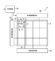
- FIG. 1 is a schematic view showing a schematic configuration of a display device according to the present embodiment.
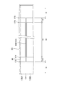
- FIG. 2 is a schematic plan view of the display panel in the display device according to the present embodiment.
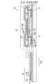
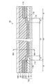
- FIG. 3 is a schematic vertical sectional view of the display panel at a position along the line III-III shown in FIG.
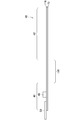
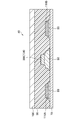
- FIG. 4 is a schematic vertical cross-sectional view of the display panel in the display device according to the present embodiment.
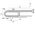
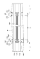
- FIG. 5 is a schematic vertical sectional view of a display panel having a curved region according to the present embodiment.
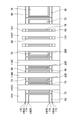
- FIG. 6 is a schematic vertical cross-sectional view of the vicinity of the curved region of the display device according to the present embodiment.
- FIG. 7 is a schematic plan view showing the manufacturing process of the display device according to the present embodiment.
- FIG. 8 is a schematic plan view showing the manufacturing process of the display device according to the present embodiment.
- FIG. 9 is a schematic plan view showing the manufacturing process of the display device according to the present embodiment.
- FIG. 10 is a schematic vertical sectional view of the display panel at a position along line XX shown in FIG.
- FIG. 11 is a schematic vertical cross-sectional view of the vicinity of the curved region of the display device according to the present embodiment.
- FIG. 12 is a schematic vertical cross-sectional view of the display panel at a position along line XII-XII shown in FIG.
- FIG. 13 is a schematic vertical cross-sectional view of the vicinity of the curved region of the display device according to the present embodiment.
- FIG. 10 is a schematic vertical sectional view of the display panel at a position along line XX shown in FIG.
- FIG. 11 is a schematic vertical cross-sectional view of the vicinity of the curved region of the display device according to the present embodiment.
- FIG. 12 is a schematic vertical
- FIG. 14 is a schematic vertical sectional view of the display panel at a position along line XIV-XIV shown in FIG.
- FIG. 15 is a schematic vertical cross-sectional view of the vicinity of the curved region of the display device according to the present embodiment.
- FIG. 16 is a schematic plan view showing the manufacturing process of the display device according to the present embodiment.
- FIG. 17 is a schematic plan view showing the manufacturing process of the display device according to the present embodiment.
- FIG. 18 is a schematic vertical cross-sectional view in the curved region of the display device according to the present embodiment.
- FIG. 19 is a schematic plan view showing the manufacturing process of the display device according to the present embodiment.
- FIG. 20 is a schematic vertical sectional view of the display panel at a position along the line XX-XX shown in FIG.
- the display device 2 is, for example, an organic electroluminescence display device, and is mounted on a television, a personal computer, a portable terminal, a mobile phone or the like.
- FIG. 1 is a schematic view showing a schematic configuration of a display device 2 according to the present embodiment.
- the display device 2 includes a pixel array unit 4 that displays an image, and a drive unit that drives the pixel array unit 4.
- the display device 2 is a flexible display, and has a wiring layer including a base made of a flexible resin film or the like, and a wiring provided inside or above the base.
- organic light emitting diodes 6 and pixel circuits 8 are arranged in a matrix corresponding to the pixels.
- the pixel circuit 8 includes a light film transistor (thin film transistor) 10, a drive TFT 12, a capacitor 14, and the like.
- the driving unit includes the scanning line driving circuit 20, the video line driving circuit 22, the driving power supply circuit 24, and the control device 26, drives the pixel circuit 8, and controls light emission of the organic light emitting diode 6.
- the scanning line driving circuit 20 is connected to a scanning signal line 28 provided for each horizontal row (pixel row) of pixels.
- the scanning line drive circuit 20 sequentially selects the scanning signal line 28 in accordance with the timing signal input from the control device 26, and applies a voltage for turning on the lighting TFT 10 to the selected scanning signal line 28.
- the video line drive circuit 22 is connected to a video signal line 30 provided for each vertical row (pixel column) of pixels.
- the video line drive circuit 22 receives a video signal from the control device 26, and in accordance with the selection of the scanning signal line 28 by the scanning line drive circuit 20, a voltage corresponding to the video signal of the selected pixel row is input to each video signal line 30. Output to The voltage is written to the capacitor 14 via the lighting TFT 10 in the selected pixel row.
- the driving TFT 12 supplies a current corresponding to the written voltage to the organic light emitting diode 6, whereby the organic light emitting diode 6 of the pixel corresponding to the selected scanning signal line 28 emits light.
- the drive power supply circuit 24 is connected to a drive power supply line 32 provided for each pixel column, and supplies a current to the organic light emitting diode 6 through the drive power supply line 32 and the drive TFT 12 of the selected pixel row.
- the lower electrode of the organic light emitting diode 6 is connected to the drive TFT 12.
- the upper electrode of each organic light emitting diode 6 is formed of an electrode common to the organic light emitting diodes 6 of all the pixels.
- the lower electrode is configured as an anode (anode)
- a high potential is input
- the upper electrode is a cathode (cathode)
- a low potential is input
- the upper electrode is an anode (anode)
- a high potential is input.
- FIG. 2 is a schematic plan view of the display panel 40 of the display device 2.
- the pixel array unit 4 shown in FIG. 1 is provided in the display area 42 of the display panel 40, and the organic light emitting diodes 6 are arranged in the pixel array unit 4 as described above.
- the upper electrode 104 constituting the organic light emitting diode 6 is formed in common to each pixel and covers substantially the entire display area 42.
- a drive portion formation region 46 is provided on one side of the display panel 40 which is a rectangle, and a wire connected to the display region 42 is disposed. Further, a driver IC 48 constituting a drive unit is mounted in the drive unit formation region 46, or an FPC (Flexible Printed Circuits) 50 is connected.
- the FPC 50 is connected to the scanning line drive circuit 20, the video line drive circuit 22, the drive power supply circuit 24, the control device 26 and the like, and an IC is mounted thereon.
- FIG. 3 is a schematic vertical sectional view of the display panel 40 at a position along the line III-III shown in FIG.
- the display panel 40 has a structure in which a circuit layer composed of a TFT 72 or the like, an organic light emitting diode 6, and a sealing layer 106 for sealing the organic light emitting diode 6 are laminated on an insulating base 70 made of a resin film. .
- a polyimide film can be used as the insulating substrate 70.
- a protective film 114 can be formed on the sealing layer 106.
- the pixel array unit 4 is a top emission type, and the light generated by the organic light emitting diode 6 is emitted on the opposite side to the insulating base 70, that is, upward in FIG.
- a color filter is disposed between the sealing layer 106 and the protective film 114 or on the opposite substrate side, and the organic light emitting diode 6 emits white light.
- the organic light emitting diode 6 emits white light.
- a color filter By generating the white light and passing the white light through a color filter, light of a color such as red (R), green (G) and blue (B) is produced.
- the pixel circuit 8 In the circuit layer of the display area 42, the pixel circuit 8, the scanning signal line 28, the video signal line 30, the driving power supply line 32, and the like described above are formed.
- at least a part of the drive unit can be formed on the insulating base 70 as a circuit layer in an area adjacent to the display area 42.
- the driver IC 48 and the FPC 50 which constitute the drive unit can be connected to the wiring 116 of the circuit layer in the drive unit formation region 46.
- polysilicon is formed on the insulating base material 70 via the first insulating film 80 as an underlayer formed of an inorganic insulating material such as silicon nitride (SiNy) or silicon oxide (SiOx).
- a film is formed, and the p-Si film is patterned to selectively leave the p-Si film at the portion used in the circuit layer.
- a semiconductor region 82 to be a channel portion and a source / drain portion of the top gate type TFT 72 is formed using a p-Si film.
- a gate electrode 86 is disposed on the channel portion of the TFT 72 via the gate insulating film 84.
- the gate electrode 86 is formed by patterning a metal film formed by sputtering or the like. Thereafter, an interlayer insulating film 88 covering the gate electrode 86 is stacked. Impurities are introduced into p-Si to be a source part and a drain part of the TFT 72 by ion implantation, and a source electrode 90a and a drain electrode 90b electrically connected to them are formed. After the TFT 72 is formed in this manner, the interlayer insulating film 92 is stacked.
- the metal film formed by sputtering or the like can be patterned on the surface of the interlayer insulating film 92 to form the wiring 94 and the like, which are used to form the metal film and the gate electrode 86, the source electrode 90a, and the drain electrode 90b.
- the wiring 116, and the scanning signal line 28, the video signal line 30, and the driving power supply line 32 shown in FIG. 1 can be formed in a multilayer wiring structure.
- an organic material such as an acrylic resin is laminated thereon to form a planarizing film 96, whereby the organic light emitting diode 6 is formed on the surface of the display area 42 planarized.
- the organic light emitting diode 6 is composed of a lower electrode 100, an organic material layer 102 and an upper electrode 104, and the lower electrode 100, the organic material layer 102 and the upper electrode 104 are sequentially stacked from the insulating base 70 side.
- the lower electrode 100 is an anode (anode) of the organic light emitting diode 6
- the upper electrode 104 is a cathode (cathode).
- the organic material layer 102 includes a hole transport layer, a light emitting layer, an electron transport layer, and the like.
- the lower electrode 100 is connected to the source electrode 90 a of the TFT 72. Specifically, after the formation of the planarizing film 96 described above, the contact hole 110 for connecting the lower electrode 100 to the TFT 72 is formed, and the conductive film formed on the surface of the planarizing film 96 and in the contact hole 110 is patterned. Then, the lower electrode 100 connected to the TFT 72 is formed for each pixel.
- a bank 112 is formed at the pixel boundary.
- the lower electrode 100 is exposed in the effective area of the pixel surrounded by the bank 112.
- the layers constituting the organic material layer 102 are sequentially stacked on the lower electrode 100.
- An upper electrode 104 is formed on the organic material layer 102 using a transparent electrode material.
- a SiNy film is formed as a sealing layer 106 on the surface of the upper electrode 104 by the CVD method.
- the protective film 114 is laminated on the surface of the display area.
- the protective film 114 is not provided in the drive portion formation region 46 in order to facilitate connection of the IC and the FPC.
- the wiring of the FPC 50 and the terminal of the driver IC 48 are electrically connected to, for example, the wiring 116.
- a display function layer including a circuit layer such as the organic light emitting diode 6 or the TFT 72 as a display element is formed on one main surface of the flexible film-like insulating substrate 70 using FIG.
- the structure of the display panel 40 has been described.
- the display panel 40 is manufactured with the entire insulating substrate 70 kept flat as shown in FIG. 3, but when stored in the housing of the display device 2, the display panel 40 is curved outward from the display area 42 of the display panel 40.
- the area 120 can be provided, and the drive portion formation area 46 can be folded back to the back side of the display area 42.
- FIGS. 4 and 5 are schematic vertical cross-sectional views of the display panel 40 corresponding to the formation of the curved region 120, and show a cross-section at a position along the line III-III shown in FIG.
- the laminated structure such as the display functional layer on the insulating substrate 70 is used as the upper structural layer 118, and in FIGS.
- FIG. 4 is a cross section in a state in which the display panel 40 is kept flat
- FIG. 5 is a sectional view in which a curved area 120 is provided between the drive area 46 and the display area 42 to which the FPC 50 and driver IC 48 are attached. Is a cross section of the display area 42 in the state of being folded back.
- the display area 42 has the pixel array section 4, and the drive section formation area 46 has a drive section for driving the pixel array section 4.
- a plurality of wirings 116 electrically connecting the pixel array unit 4 and the drive unit are disposed in the upper structural layer 118 in the curved region 120 connecting the display region 42 and the drive unit formation region 46. .
- the display panel 40 includes a spacer 256, a front reinforcing film 254, a back reinforcing film 258, an FPC 50, and a driver IC 48. .
- the front reinforcing film 254 and the back reinforcing film 258 are provided to protect and reinforce the insulating base 70 and the upper structural layer 118.
- the spacers 256 are provided to guide the curvature of the insulating substrate 70 and the upper structural layer 118.
- a display area 42 for displaying an image, a curved area 120, and a drive portion forming area 46 are provided side by side in this order.
- the curved region 120 has a curved shape along the shape of the guide portion 256A of the spacer 256.
- the drive portion forming area 46 is disposed on the back side of the spacer 256 by the bending of the curved area 120.
- the front reinforcing film 254 is provided on the display surface side of the display area 42 of the display panel 40 so as not to overlap with the curved area 120.
- the back reinforcing film 258 is provided between the insulating base 70 and the spacer 256 in the display area 42, and is driven with a first reinforcing portion 258A attached to the insulating base 70, and a drive.
- the second reinforcing portion 258B provided between the insulating base 70 and the spacer 256 in the portion forming area 46 and attached to the insulating base 70, and the insulating base 70 and the spacer 256 in the curved area 120.
- a curved reinforcing portion 258C attached to the insulating substrate 70.
- the second reinforcing portion 258B of the back reinforcing film 258 is attached to the surface on the back side of the spacer 256 by the bonding member 266, and the first reinforcing portion 258A of the back reinforcing film 258 is
- the adhesive member 262 is attached to the surface on the display surface side of the spacer 256.
- the adhesive member 262 and the adhesive member 266 may be made of an adhesive resin or the like, or may be a double-sided tape or the like.
- the curved reinforcing portion 258C is not bonded to the spacer 256 by an adhesive member, but an adhesive member may be provided also on the guide portion 256A of the spacer 256.
- a resin having adhesiveness as an adhesive member may be filled in the space between the curved reinforcing portion 258C and the spacer 256, and the curved reinforcing portion 258C and the guide portion 256A of the spacer 256 may be directly bonded.
- the spacer 256 has a shape in which a guide portion 256A for guiding the curvature of the curved area 120 of the display panel 40 is rounded in a cross sectional view. With such a shape, disconnection or breakage of the wiring 116 and the like in the curved region 120 of the display panel 40 is unlikely to occur.
- the back reinforcing film 258 is provided on the inner surface side of the curvature of the curved region 120, the stress generated in the display panel 40 can be alleviated, and the disconnection of the wiring 116 of the display panel 40 is suppressed. be able to.
- the stress is most likely to occur in the curved region, since the curved reinforcing portion 258C is provided in the curved region 120, the stress is more easily relaxed.
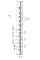
- FIG. 6 is a schematic vertical cross-sectional view of the vicinity of the curved region 120 of the display device 2 according to the present embodiment.
- a first laminate of silicon nitride (SiNy) and silicon oxide (SiOx) or the like is formed on the upper surface of the insulating base 70 made of polyimide or the like.
- the insulating film 80 is formed.
- a second insulating film 134 is formed on the upper surface of the first insulating film 80.
- the second insulating film 134 corresponds to, for example, the gate insulating film 84 or the interlayer insulating film 88 shown in FIG. Similar to the first insulating film 80, the second insulating film 134 can be formed using silicon nitride (SiNy), silicon oxide (SiOx), or the like.
- the insulating substrate 70, the first insulating film 80, and the second insulating film 134 constitute an insulating sheet 132.
- the first insulating film 80 and the second insulating film 134 are inorganic insulating films, and the insulating base 70 is an organic insulating film.
- FIG. 7 is a top view showing a state after the second insulating film 134 is formed.
- the second insulating film 134 is not provided in most of the curved region 120, but is provided only between the two wiring formation regions 136A and 136B where the wiring 116 is formed.
- the second insulating film 134 provided between the two wiring formation regions 136A and 136B serves as the insulating wall 200.
- the second insulating film 134 is not provided in most of the curved region 120 except the region where the insulating wall 200 is formed, whereby the insulating sheet 132 shown in FIG. Stiffness can be reduced.
- the film thickness of the insulating sheet 132 is a first film thickness thinner than the film thickness of the display region 42 and the film thickness of the drive portion formation region 46. This region is defined as a first film thickness region 126.
- a first stepped portion 170 is formed between the first film thickness region 126 and the display region 42, and a second stepped portion between the first film thickness region 126 and the drive portion formation region 46. 172 is formed.
- the insulating wall 200 extends from the first stepped portion 170 to the second stepped portion 172.
- the top surface of the second insulating film 134 and the top surface of the insulating wall 200 are continuous. That is, the upper surface of the insulating wall 200 is continuous with the upper surface of the insulating sheet 132 in the display area 42 and the drive portion forming area 46. This is because, in the process of forming the second insulating film 134, the insulating wall 200 and the second insulating film 134 are simultaneously formed using the same material.
- the insulating sheet 132 is a second film thickness region having a second film thickness thinner than the first film thickness on the center side of the first film thickness region 126. It has 128.
- the curved region 120 can realize a further decrease in the rigidity of the insulating sheet 132 by having a thinner second film thickness region 128.
- a third step portion 174 is formed at the boundary between the first film thickness region 126 and the second film thickness region 128.
- the wiring 116 is provided on the upper surface of the second insulating film 134 and the upper surface of the first insulating film 80 in the curved region 120.
- the wiring 116 is processed into the shape of the wiring 116 by dry etching after the wiring layer is formed on the entire surface of the insulating sheet 132 by sputtering, for example.
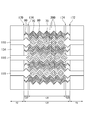
- FIG. 8 is a top view showing a state in which the first wiring 116A and the second 116B are formed by dry etching after the wiring layer is formed.
- the first wires 116A and the second wires 116B run parallel to each other, and electrically connect the pixel array unit 4 provided in the display area 42, and the driver IC 48 and the like constituting the drive unit provided in the drive unit formation area 46.
- Connected to The first wiring 116A and the second wiring 116B cross the first step portion 170 and the second step portion 172, respectively. Further, in the present embodiment, the first wiring 116A and the second wiring 116B both cross the third step portion 174.
- first wiring 116A and the second wiring 116B are formed only in the portions scheduled for the wiring formation regions 136A and 136B described above with reference to FIG.
- first step 170 and the second step 172 there is a possibility that the first conductor 140A which could not be removed in the dry etching step may remain. is there.
- the second conductor 140B that could not be removed in the dry etching step may remain.
- the display panel 40 since the display panel 40 has the insulating wall 200 formed before the formation of the conductor 140, the first conductor 140A which can not be completely removed in the dry etching process, It can be suppressed that the second conductor 140B electrically connects the first wiring 116A and the second wiring 116B.
- the third conductor 140C which can not be completely removed in the dry etching step remains even in the step portion at the boundary between the insulating wall 200 forming portion and the insulating wall 200 non-forming portion.
- the insulating wall 200 is configured to extend from the first stepped portion 170 to the second stepped portion 172 between the first wiring 116A and the second wiring 116B, the third conductor 140C
- the first conductor 140A remaining on one side of the insulating wall 200 and the first conductor 140A remaining on the other side of the insulating wall 200 can be prevented from being electrically connected, and as a result thereof It is possible to suppress the electrical connection between the first first wiring 116A and the second wiring 116B.
- the first wiring 116A and the second wiring 116B are formed, as shown in FIG. 9, the first wiring 116A of the first insulating film 80 in the second film thickness region 128, the second The region where the wiring 116B is not formed may be etched to expose the upper surface of the insulating base 70 from a part or the entire surface of the first insulating film 80. With such a configuration, it is possible to realize a further reduction in the rigidity of the insulating sheet 132.
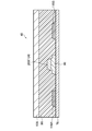
- an inorganic insulating film 150 is formed covering the top and side surfaces of the first wiring 116A and the second wiring 116B.
- the inorganic insulating film 150 is formed using, for example, silicon nitride or the like.
- planarizing film 96 is formed on the exposed upper surface of the display region 42 and the inorganic insulating film 150 in the drive portion formation region 46, and the first insulating film 80 and the second insulating film 134.
- the planarization film 96 is formed using, for example, polyimide.
- a sealing layer 106 which seals the entire top surface of the display panel 40 is formed.
- the sealing layer 106 is formed using, for example, a silicon nitride film as described above.
- the planarizing film 96 may be provided in all the regions 42, the curved region 120, and the drive portion formation region 46.
- the inorganic insulating film 150 is provided in all of the display region 42, the curved region 120, and the drive portion forming region 46 , but as shown in FIGS. It may be formed only in the display area 42, and the inorganic insulating film 150 may not be provided in the curved area 120 and the drive part formation area 46. Since the planarization film 96, the sealing layer 106, and the like cover the upper surfaces and the side surfaces of the plurality of wirings 116, the insulating film between the planarization film 96 and the sealing layer 106 has a plurality of wirings 116 without providing the inorganic insulating film 150. Can be secured. In the embodiment shown in FIGS.
- the upper surface of the insulating base 70 is exposed from the entire surface of the first insulating film 80 in the second film thickness region 128, and the second film thickness region 128 is exposed.
- the wiring 116 is provided on the upper surface of the insulating base 70. That is, the film thickness of the insulating sheet 132 in the second film thickness region 128 is only the thickness of the insulating base material 70. With such a configuration, the rigidity in the curved region 120 can be further reduced.
- the step reduction layer 160 is interposed between the second insulating film 134 and the first insulating film 80. It is desirable to provide it.
- the step difference relaxation layer 160 is formed on the upper surface of the first insulating film 80, and is formed so that a part thereof protrudes from the lower surface of the second insulating film 134.
- Step reduction layer 160 can be formed using, for example, a polysilicon film or the like.
- the first insulating film 80 is not provided below the wiring 116, whereby the risk of the wiring 116 being broken can be reduced. That is, generally, the inorganic insulating film has a high risk of being broken as it is bent. Therefore, there is a risk that the first insulating film 80 which is an inorganic insulating film is broken when the curved region 120 is bent.
- the first insulating film 80 since the first insulating film 80 is not provided below the wiring 116 in the curved region 120, the bending of the curved region 120 is caused. It is possible to suppress the first insulating film 80 from being broken. As a result, it is possible to reduce the risk that the wiring 116 is broken due to the impact accompanying the crack of the first insulating film 80.
- the configuration in which the insulating wall 200 is integrally formed with the second insulating film 134 is described as an example, but the insulating wall 200 and the second insulating film 134 are separately configured. It may be However, as shown in this embodiment, the manufacturing cost can be reduced by integrally forming the insulating wall 200 and the second insulating film 134 with the same material.
- the possibility of the first wiring 116A and the second wiring 116B being electrically connected is further reduced. be able to. That is, the highest risk that the first wiring 116A and the second wiring 116B are electrically connected is because the first conductor 140A may remain due to the difference in level that has arisen in the vicinity of the insulating wall 200.
- the boundary region between the first insulating film 80 and the second insulating film 134 which is the boundary region between the first insulating film 80 and the second insulating film 134, corresponds to the second insulating film 134 and the insulating wall 200.
- the stress applied at the time of forming the curved region 120 causes the second insulating film 134 and the insulating wall 200 to split.
- the possibility of electrically connecting the first wiring 116A and the second wiring 116B can be further reduced.
- the above-described insulating wall 200 is provided between the plurality of signal lines 116C, 116D, and 116E having different potentials, whereby the signal line 116C, the signal line 116D, and the signal lines It is desirable that electrical connection between the signal line 116D and the signal line 116E can be suppressed by the first conductor 140A and the second conductor 140B that can not be removed in the dry etching step.
- the signal line 116E and the power supply line 116F can be the first conductor 140A and the second conductor 140B. Is desirable because it can suppress electrical connection.
- the power supply line 116F in the case where an opening is provided in the power supply line 116F in order to reduce the rigidity of the curved region 120, it is necessary to provide the insulating wall 200 in the opening formation region. There is no. The potential of the power supply line 116F does not change between the right side and the left side of the opening, and there is no problem even if it is electrically connected by the first conductor 140A and the second conductor 140B that could not be removed in the dry etching process. It is. Further, by not providing the insulating wall 200 in the opening formation region, the power supply line 116F can be formed with a limited area, and the area reduction of the display device 2 can be achieved.
- each wire 116 has a shape in which a plurality of rhombuses are combined
- a curve according to the apex of the rhombus It is desirable to have a zigzag shape having a portion. With such a configuration, the wirings 116 and the insulating wall 200 can be disposed closer to each other. Furthermore, the bending resistance of each wire 116 itself is also increased.
- the conductor is removed by etching or the like on the inner side of the rhombus shape in each wiring 116 to form an opening and expose the first insulating film 80 and the insulating base 70.
Landscapes
- Engineering & Computer Science (AREA)
- Microelectronics & Electronic Packaging (AREA)
- Physics & Mathematics (AREA)
- General Physics & Mathematics (AREA)
- Theoretical Computer Science (AREA)
- Devices For Indicating Variable Information By Combining Individual Elements (AREA)
- Electroluminescent Light Sources (AREA)
Abstract
本開示に係る表示装置は、表示領域(42)から駆動部形成領域(46)にまで設けられ、且つ湾曲領域(120)において、表示領域(42)の膜厚及び駆動部形成領域(46)の膜厚よりも薄い第1の膜厚を有する第1の膜厚領域(126)を有し、表示領域(42)と第1の膜厚領域(126)との間に配置された第1の段差部(170)と、駆動部形成領域(46)と第1の膜厚領域(126)との間に配置された第2の段差部(172)とを有する絶縁性シート(134)と、絶縁性シート(134)の上方において、第1の段差部(170)と、第2の段差部(172)とを横切り、且つ表示領域(42)と駆動部形成領域(46)とを電気的に接続する第1の配線(116A)、及び第2の配線(116B)と、第1の配線(116A)と第2の配線(116B)との間において、第1の段差部(170)から第2の段差部(172)まで延伸する絶縁壁(200)と、を含む。
Description
本発明は、表示装置に関する。
有機エレクトロルミネッセンス(electroluminescence:EL)表示装置などのフラットパネルディスプレイは基板上に薄膜トランジスタ(thin film transistor:TFT)や有機発光ダイオード(organic light-emitting diode:OLED)などが形成された表示パネルを有する。表示パネルの基材には従来、ガラス基板が用いられていたが近年、当該基材にポリイミド膜などの樹脂フィルム等を用いて、表示パネルを曲げることができるフレキシブルディスプレイの開発が進められている。
フレキシブルディスプレイの用途として、表示パネルの画像表示領域より外側に設けられる、集積回路(integrated circuit:IC)やフレキシブルプリント基板(flexible printed circuit:FPC)の実装部を表示領域の裏側に折り曲げて狭額縁化を図ることが考えられている。
下記特許文献1においては、実装部を表示領域の裏面側に折り曲げることにより形成される湾曲領域において、絶縁性シートの上面に電位の異なる複数の配線を設ける構成が開示されている。
しかし、上記従来の構成においては、電位の異なる複数の配線間におけるショート抑制が十分ではなかった。即ち、上記湾曲領域においては、絶縁性シートの剛性を下げる必要があるため、絶縁性シートの膜厚を薄くすることが望ましい。しかし、絶縁性シートの膜厚を段階的に薄くすると、複数の配線間を連絡する段差部が生じうる。この段差部においては、絶縁性シートの上面に配線層を形成した後にドライエッチング等により当該配線層を配線形状に加工する際に、不要な配線層が除去されず残存してしまう可能性がある。その結果として、この配線層の残存部が、電位の異なる複数の配線間を電気的に接続してしまうことによってショートが発生する恐れがあった。
本発明は、上記問題点に鑑みてなされたものであり、その目的は、湾曲領域における電位の異なる複数の配線間のショート抑制を図ることである。
(1)本開示に係る表示装置は、画素アレイ部を有する表示領域と、前記表示領域の裏面側に設けられ、前記画素アレイ部を駆動する駆動部を有する駆動部形成領域と、前記表示領域と駆動部形成領域とを連結する湾曲領域と、を有する表示パネルを含み、前記表示パネルは、前記表示領域から前記駆動部形成領域にまで設けられ、且つ前記湾曲領域において、前記表示領域の膜厚及び前記駆動部形成領域の膜厚よりも薄い第1の膜厚を有する第1の膜厚領域を有し、前記表示領域と前記第1の膜厚領域との間に配置された第1の段差部と、前記駆動部形成領域と前記第1の膜厚領域との間に配置された第2の段差部とを有する絶縁性シートと、前記絶縁性シートの上方において、前記第1の段差部と、前記第2の段差部とを横切り、且つ前記画素アレイ部と前記駆動部とを電気的に接続する第1の配線、及び第2の配線と、前記第1の配線と前記第2の配線との間において、前記第1の段差部から前記第2の段差部まで延伸する絶縁壁と、を含む。
(2)上記(1)における表示装置において、前記絶縁壁の上面が、前記表示領域、及び前記駆動部形成領域における前記絶縁性シートの上面と連続してもよい。
(3)上記(1)~(2)における表示装置が、前記第1の段差部と前記第2の段差部に配置された第1の導体を含んでよい。
(4)上記(1)~(3)における表示装置において、前記絶縁性シートが、前記第1の膜厚領域の中央側において、前記第1の膜厚よりも薄い第2の膜厚を有する第2の膜厚領域を有し、前記第1の配線と前記第2の配線の内の少なくとも一方が、前記第1の膜厚領域と前記第2の膜厚領域との間に配置された第3の段差部を横切るよう配置されてもよい。
(5)上記(4)における表示装置が、前記第3の段差部に配置された第2の導体を含んでもよい。
(6)上記(4)、(5)における表示装置において、前記絶縁性シートは、絶縁性基材と、前記絶縁性基材上に設けられた第1の絶縁膜と、を含み、前記第2の膜厚領域において、前記第1の絶縁膜の少なくとも一部から前記絶縁性基材の上面が露出されてもよい。
(7)上記(6)における表示装置において、前記絶縁性基材はポリイミドからなってもよい。
(8)上記(6)における表示装置において、記第1の絶縁膜は酸化シリコン層と窒化シリコン層との積層体からなってもよい。
(9)上記(6)における表示装置において、前記絶縁性シートは、前記表示領域における前記第1の絶縁膜と前記第1の配線との間、及び前記第1の絶縁膜と前記第2の配線との間に、第2の絶縁膜を更に含んでもよい。
(10)上記(9)における表示装置において、前記第2の絶縁膜と前記第1の絶縁膜との間に、段差緩和層が設けられてもよい。
(11)上記(9)、(10)における表示装置において、前記絶縁壁の少なくとも一部が、前記第2の絶縁膜と同一材料で構成されてもよい。
(12)上記(1)~(11)における表示装置において、前記第1の配線と前記第2の配線とは電位が異なる信号線であってもよい。
(13)本開示に係る表示装置は、画素アレイ部を有する表示領域と、前記表示領域の裏面側に設けられ、前記画素アレイ部を駆動する駆動部を有する駆動部形成領域と、前記表示領域と駆動部形成領域とを連結する湾曲領域と、を有する表示パネルを含み、前記表示パネルは、有機材料で構成された絶縁性基材と、前記絶縁性基材上に設けられ、無機絶縁材料で構成され、前記表示領域から前記駆動部形成領域にまで設けられ、且つ前記湾曲領域において、前記表示領域の膜厚及び前記駆動部形成領域の膜厚よりも薄い第1の膜厚を有する第1の膜厚領域を有し、前記表示領域と前記第1の膜厚領域との間に配置された第1の段差部と、前記駆動部形成領域と前記第1の膜厚領域との間に配置された第2の段差部とを有する無機絶縁膜と、前記無機絶縁膜の上方において、前記第1の段差部と、前記第2の段差部とを横切り、且つ前記画素アレイ部と前記駆動部とを電気的に接続する第1の配線、及び第2の配線と、前記第1の配線と前記第2の配線との間において、前記第1の段差部から前記第2の段差部まで延伸する絶縁壁と、を含む。
(14)上記(13)における表示装置において、前記絶縁壁の上面が、前記表示領域、及び前記駆動部形成領域における前記無機絶縁膜の上面と連続してもよい。
(15)上記(13)、(14)における表示装置において、前記第1の段差部と前記第2の段差部に配置された第1の導体を含んでもよい。
(16)上記(13)~(15)における表示装置において、前記無機絶縁膜が、前記第1の膜厚領域の中央側において、前記第1の膜厚よりも薄い第2の膜厚を有する第2の膜厚領域を有し、前記第1の配線と前記第2の配線の内の少なくとも一方が、前記第1の膜厚領域と前記第2の膜厚領域との間に配置された第3の段差部を横切るよう配置されてもよい。
(17)上記(13)における表示装置において、前記無機絶縁膜は、前記絶縁性基材と前記第1の配線および第2の配線との間に配置された第1の絶縁膜と、前記第1の絶縁膜と前記第1の配線および第2の配線との間に配置された第2の絶縁膜を含んでもよい。
(18)上記(17)における表示装置において、前記第2の絶縁膜と前記第1の絶縁膜との間に、段差緩和層が設けられてもよい。
(19)上記(17)、(18)における表示装置において、前記絶縁壁の少なくとも一部が、前記第2の絶縁膜と同一材料で構成されてもよい。
[第1の実施形態]
以下、本発明の実施の形態について、図面に基づいて説明する。
以下、本発明の実施の形態について、図面に基づいて説明する。
なお、本開示はあくまで一例にすぎず、当業者において、発明の主旨を保っての適宜変更について容易に想到し得るものについては、当然に本発明の範囲に含有されるものである。また、図面は説明をより明確にするため、実際の態様に比べ、各部の幅、厚さ、形状等について模式的に表される場合があるが、あくまで一例であって、本発明の解釈を限定するものではない。また、本明細書と各図において、既出の図に関して前述したものと同様の要素には、同一の符号を付して、詳細な説明を適宜省略することがある。さらに特に断りのない限り、本発明の実施形態同士は互いに組み合わせることが可能である。
本実施形態に係る表示装置2は、例えば有機エレクトロルミネッセンス表示装置であり、テレビ、パソコン、携帯端末、携帯電話等に搭載される。図1は本実施形態に係る表示装置2の概略の構成を示す模式図である。表示装置2は、画像を表示する画素アレイ部4と、当該画素アレイ部4を駆動する駆動部とを備える。表示装置2はフレキシブルディスプレイであり、可撓性を有した樹脂フィルムなどからなる基材と、当該基材の内部又は上方に設けられた配線と、を含む配線層を有する。
画素アレイ部4には画素に対応して有機発光ダイオード6及び画素回路8がマトリクス状に配置される。画素回路8は、点灯TFT(thin film transistor)10、駆動TFT12、及びキャパシタ14などを含む。
一方、駆動部は、走査線駆動回路20、映像線駆動回路22、駆動電源回路24及び制御装置26を含み、画素回路8を駆動し、有機発光ダイオード6の発光を制御する。
走査線駆動回路20は画素の水平方向の並び(画素行)ごとに設けられた走査信号線28に接続されている。走査線駆動回路20は制御装置26から入力されるタイミング信号に応じて走査信号線28を順番に選択し、選択した走査信号線28に、点灯TFT10をオンする電圧を印加する。
映像線駆動回路22は画素の垂直方向の並び(画素列)ごとに設けられた映像信号線30に接続されている。映像線駆動回路22は制御装置26から映像信号を入力され、走査線駆動回路20による走査信号線28の選択に合わせて、選択された画素行の映像信号に応じた電圧を各映像信号線30に出力する。当該電圧は、選択された画素行にて点灯TFT10を介してキャパシタ14に書き込まれる。駆動TFT12は書き込まれた電圧に応じた電流を有機発光ダイオード6に供給し、これにより、選択された走査信号線28に対応する画素の有機発光ダイオード6が発光する。
駆動電源回路24は画素列ごとに設けられた駆動電源線32に接続され、駆動電源線32及び選択された画素行の駆動TFT12を介して有機発光ダイオード6に電流を供給する。
ここで、有機発光ダイオード6の下部電極は駆動TFT12に接続される。一方、各有機発光ダイオード6の上部電極は、全画素の有機発光ダイオード6に共通の電極で構成される。下部電極を陽極(アノード)として構成する場合は、高電位が入力され、上部電極は陰極(カソード)となって低電位が入力される。下部電極を陰極(カソード)として構成する場合は、低電位が入力され、上部電極は陽極(アノード)となって高電位が入力される。
図2は表示装置2の表示パネル40の模式的な平面図である。表示パネル40の表示領域42に図1に示した画素アレイ部4が設けられ、上述したように画素アレイ部4には有機発光ダイオード6が配列される。上述したように有機発光ダイオード6を構成する上部電極104は各画素に共通に形成され、表示領域42の略全体を覆う。
矩形である表示パネル40の一辺には駆動部形成領域46が設けられ、表示領域42につながる配線が配置される。さらに駆動部形成領域46には駆動部を構成するドライバIC48が搭載されたり、FPC(Flexible Printed Circuits)50が接続されたりする。FPC50は走査線駆動回路20、映像線駆動回路22、駆動電源回路24及び制御装置26等に接続されたり、その上にICを搭載されたりする。
図3は図2に示すIII-III線に沿った位置での表示パネル40の模式的な垂直断面図である。表示パネル40は、樹脂フィルムからなる絶縁性基材70の上にTFT72などからなる回路層、有機発光ダイオード6、及び有機発光ダイオード6を封止する封止層106などが積層された構造を有する。絶縁性基材70として例えば、ポリイミド膜を用いることができる。封止層106の上には保護膜114を形成することができる。本実施形態において画素アレイ部4はトップエミッション型であり、有機発光ダイオード6で生じた光は絶縁性基材70とは反対側、つまり図3において上向きに出射される。なお、表示装置2におけるカラー化方式をカラーフィルタ方式とする場合には封止層106と保護膜114との間、あるいは対向基板側にカラーフィルタが配置され、有機発光ダイオード6にて白色光を生成し、当該白色光をカラーフィルタに通すことで例えば、赤(R)、緑(G)、青(B)などの色の光を作る。
表示領域42の回路層には、上述した画素回路8、走査信号線28、映像信号線30、駆動電源線32などが形成される。また、駆動部の少なくとも一部分は絶縁性基材70上に回路層として表示領域42に隣接する領域に形成することができる。また上述したように駆動部を構成するドライバIC48やFPC50を駆動部形成領域46にて、回路層の配線116に接続することができる。
具体的には絶縁性基材70の上に窒化シリコン(SiNy)や酸化シリコン(SiOx)などの無機絶縁材料からなる下地層としての第1の絶縁膜80を介してポリシリコン(p-Si)膜が形成され、当該p-Si膜をパターニングし、回路層で用いる箇所のp-Si膜を選択的に残す。例えば、p-Si膜を用いてトップゲート型のTFT72のチャネル部及びソース・ドレイン部となる半導体領域82が形成される。TFT72のチャネル部の上にはゲート絶縁膜84を介してゲート電極86が配置される。ゲート電極86はスパッタリング等で形成した金属膜をパターニングして形成される。この後、ゲート電極86を覆う層間絶縁膜88を積層する。TFT72のソース部、ドレイン部となるp-Siにはイオン注入により不純物が導入され、さらにそれらに電気的に接続されたソース電極90a及びドレイン電極90bが形成される。このようにしてTFT72を形成した後、層間絶縁膜92を積層する。層間絶縁膜92の表面には、スパッタリング等で形成した金属膜をパターニングして配線94等を形成することができ、当該金属膜とゲート電極86、ソース電極90a及びドレイン電極90bの形成に用いた金属膜とで例えば、配線116、及び図1に示した走査信号線28、映像信号線30、駆動電源線32を多層配線構造で形成することができる。この上に例えば、アクリル樹脂等の有機材料を積層して平坦化膜96が形成され、これにより平坦化された表示領域42の表面に有機発光ダイオード6が形成される。
有機発光ダイオード6は下部電極100、有機材料層102及び上部電極104で構成され、これら下部電極100、有機材料層102及び上部電極104は絶縁性基材70側から順に積層される。本実施形態では下部電極100が有機発光ダイオード6の陽極(アノード)であり、上部電極104が陰極(カソード)である。有機材料層102は正孔輸送層、発光層、電子輸送層等を含んで構成される。
図3に示すTFT72がnチャネルを有した駆動TFT12であるとすると、下部電極100はTFT72のソース電極90aに接続される。具体的には、上述した平坦化膜96の形成後、下部電極100をTFT72に接続するためのコンタクトホール110が形成され、平坦化膜96表面及びコンタクトホール110内に形成した導電体膜をパターニングして、TFT72に接続された下部電極100が画素ごとに形成される。
下部電極100の形成後、画素境界にバンク112を形成する。バンク112で囲まれた画素の有効領域には下部電極100が露出する。バンク112の形成後、有機材料層102を構成する各層が下部電極100の上に順番に積層される。有機材料層102の上に上部電極104が透明電極材料を用いて形成される。
上部電極104の表面に封止層106として例えば、SiNy膜がCVD法によって成膜される。また、表示パネル40の表面の機械的な耐性を確保するため、表示領域42の表面に保護膜114が積層される。一方、駆動部形成領域46にはICやFPCを接続し易くするため保護膜114を設けない。FPC50の配線やドライバIC48の端子は例えば、配線116に電気的に接続される。
以上、図3を用いて、可撓性を備えたフィルム状の絶縁性基材70の一方の主面上に表示素子である有機発光ダイオード6やTFT72などの回路層を含む表示機能層を形成した表示パネル40の構造を説明した。
表示パネル40は図3に示すように絶縁性基材70全体を平面に保って製造されるが、表示装置2の筐体に格納する際には、表示パネル40の表示領域42より外側に湾曲領域120を設けて駆動部形成領域46を表示領域42の裏側に折り返した状態とすることができる。図4、図5はこの湾曲領域120の形成に対応した表示パネル40の模式的な垂直断面図であり、図2に示すIII-III線に沿った位置での断面を示している。図3に示した表示パネル40の積層構造のうち絶縁性基材70上の表示機能層などの積層構造を上部構造層118として、図4、5では図3の構造を絶縁性基材70と上部構造層118との2層構造に簡略化して示している。図4は表示パネル40が平面に保たれた状態での断面であり、図5はFPC50やドライバIC48を取り付ける駆動部形成領域46と表示領域42との間に湾曲領域120を設けて、FPC50などを表示領域42の裏側に折り返した状態の断面である。
上述したとおり、表示領域42は画素アレイ部4を有し、駆動部形成領域46はこの画素アレイ部4を駆動する駆動部を有する。そして、表示領域42と駆動部形成領域46とを連結する湾曲領域120には、画素アレイ部4と駆動部とを電気的に接続する複数の配線116が上部構造層118内に配置されている。
図5に示すように、表示パネル40は、絶縁性基材70、上部構造層118に加えて、スペーサ256と、表補強フィルム254と、裏補強フィルム258と、FPC50と、ドライバIC48とを有する。表補強フィルム254、及び裏補強フィルム258は、絶縁性基材70、及び上部構造層118を保護、補強するために設けられる。スペーサ256は、絶縁性基材70、及び上部構造層118の湾曲をガイドするために設けられる。
表示パネル40には、画像表示を行う表示領域42と、湾曲領域120と、駆動部形成領域46とが、この順で並んで設けられる。湾曲領域120は、スペーサ256のガイド部256Aの形状に沿うように湾曲した形状となっている。駆動部形成領域46は、湾曲領域120が湾曲することにより、スペーサ256の背面側に配置されている。
表補強フィルム254は、図5に示すように、表示パネル40の、表示領域42の表示面側に、湾曲領域120に重ならないように設けられる。
裏補強フィルム258は、図5に示すように、表示領域42における絶縁性基材70とスペーサ256との間に設けられ、絶縁性基材70に貼り付けられた第1補強部258Aと、駆動部形成領域46における絶縁性基材70とスペーサ256との間に設けられ、絶縁性基材70に張り付けられた第2補強部258Bと、湾曲領域120における絶縁性基材70とスペーサ256との間に設けられ、絶縁性基材70に張り付けられた湾曲補強部258Cとを有する。
また、図5に示すように、裏補強フィルム258の第2補強部258Bは、接着部材266によりスペーサ256の背面側の表面に貼り付けられており、裏補強フィルム258の第1補強部258Aは、接着部材262によりスペーサ256の表示面側の表面に貼り付けられている。なお、接着部材262及び接着部材266は、粘着性を有する樹脂等からなるものでもよいし、両面テープ等でもよい。なお、図5に示す例においては、湾曲補強部258Cはスペーサ256に対して接着部材により接着されていないが、スペーサ256のガイド部256Aにも接着部材を設けてもよい。また、例えば、接着部材として粘着性を有する樹脂を湾曲補強部258Cとスペーサ256との間の空間に充填し、湾曲補強部258Cとスペーサ256のガイド部256Aとを直接接着してもよい。
スペーサ256は、図5に示すように、断面視において、表示パネル40の湾曲領域120の湾曲をガイドするガイド部256Aが丸まった形状をしている。このような形状を有するため、表示パネル40の湾曲領域120において配線116等の断線や破損が生じにくい。
本実施形態においては、湾曲領域120の湾曲の内面側に、裏補強フィルム258を設ける構成を採用するため、表示パネル40に生じる応力を緩和でき、表示パネル40の配線116の断線等を抑制することができる。また、応力は湾曲領域に最も生じやすいが、湾曲領域120に湾曲補強部258Cが設けられるため、応力をより緩和しやすい構成となっている。
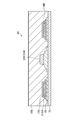
図6は、本実施形態に係る表示装置2の湾曲領域120付近の模式的な垂直断面図である。図6に示すように、表示領域42から駆動部形成領域46にかけて、ポリイミド等からなる絶縁性基材70の上面に、窒化シリコン(SiNy)と酸化シリコン(SiOx)の積層体等からなる第1の絶縁膜80が形成されている。
表示領域42、及び駆動部形成領域46においては、この第1の絶縁膜80の上面に第2の絶縁膜134が形成されている。この第2の絶縁膜134は、例えば図3に示したゲート絶縁膜84や、層間絶縁膜88等に対応する。第2の絶縁膜134は、第1の絶縁膜80と同様、窒化シリコン(SiNy)や酸化シリコン(SiOx)等を用いて形成することができる。これら絶縁性基材70、第1の絶縁膜80、第2の絶縁膜134が、絶縁性シート132を構成している。第1の絶縁膜80および第2の絶縁膜134は無機絶縁膜であり、絶縁性基材70は有機絶縁膜である。
図7は、第2の絶縁膜134を形成した後の状態を示す上面図である。図7に示すように、第2の絶縁膜134は、湾曲領域120においては、そのほとんどの領域において設けられず、配線116が形成される2本の配線形成領域136A、136Bの間のみに設けられる。この2本の配線形成領域136A、136Bの間に設けられた第2の絶縁膜134が絶縁壁200となる。このように、絶縁壁200形成領域を除き、湾曲領域120のほとんどの領域において第2の絶縁膜134を設けない構成とすることにより、図6に示した絶縁性シート132の、湾曲領域120における剛性を下げることができる。剛性が低下することで、湾曲領域120の無機絶縁膜の曲げに伴う割れリスクが低減する。尚、有機膜や金属膜は曲げに伴う割れリスクが高くない。この第2の絶縁膜134を設けない領域は、絶縁性シート132の膜厚が、表示領域42の膜厚及び前記駆動部形成領域46の膜厚よりも薄い第1の膜厚となっており、この領域を第1の膜厚領域126と定義する。この第1の膜厚領域126と表示領域42との間には第1の段差部170が形成され、第1の膜厚領域126と駆動部形成領域46との間には第2の段差部172が形成される。絶縁壁200は、この第1の段差部170から第2の段差部172まで延伸している。
なお、本実施形態においては、第2の絶縁膜134の上面と絶縁壁200の上面とが連続する構成としている。即ち、絶縁壁200の上面が、表示領域42、駆動部形成領域46における絶縁性シート132の上面と連続している。これは、第2の絶縁膜134を形成する工程において、同一材料を用いて絶縁壁200と第2の絶縁膜134とを同時に形成するためである。
更に、図6、7に示すように、絶縁性シート132は、第1の膜厚領域126の中央側において、第1の膜厚よりも薄い第2の膜厚を有する第2の膜厚領域128を有している。湾曲領域120は、より膜厚の薄い第2の膜厚領域128を有することで、絶縁性シート132の更なる剛性の低下を実現することができる。第1の膜厚領域126と第2の膜厚領域128との境界部には第3の段差部174が形成されている。
図6に示すように、第2の絶縁膜134の上面、及び湾曲領域120における第1の絶縁膜80の上面には、配線116が設けられる。配線116は、例えばスパッタなどにより配線層を絶縁性シート132の全面に形成した後、ドライエッチングを施すことにより、配線116の形状に加工する。
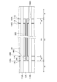
図8は、配線層を形成した後に、ドライエッチングにより第1の配線116A、第2の116Bを形成した状態を示す上面図である。第1の配線116A、第2の116Bは互いに並走し、表示領域42に設けられた画素アレイ部4と、駆動部形成領域46に設けられた駆動部を構成するドライバIC48等とを電気的に接続している。第1の配線116A、第2の配線116Bは、ともに第1の段差部170、第2の段差部172を横切っている。また、本実施形態においては、第1の配線116A、第2の配線116Bは、ともに第3の段差部174を横切っている。
本来は、図7を用いて上述した配線形成領域136A、136Bに予定していた部分のみに第1の配線116A、第2の配線116Bを形成することが望ましい。しかし、実際には、図8に示すように、第1の段差部170、第2の段差部172において、ドライエッチング工程において除去しきれなかった第1の導体140Aが残存してしまう可能性がある。
更に、上述したとおり、第3の段差部174においても、ドライエッチング工程において除去しきれなかった第2の導体140Bが残存してしまう可能性がある。
しかし、本実施形態においては図8に示すように、表示パネル40が、導体140形成前に形成された絶縁壁200を有するため、ドライエッチング工程で除去しきれなかった第1の導体140A、第2の導体140Bが、第1の配線116Aと第2の配線116Bとを電気的に接続してしまうことを抑制することができる。
なお、この絶縁壁200を設けた場合、絶縁壁200形成部と絶縁壁200非形成部との境界における段差部においても、ドライエッチング工程において除去しきれなかった第3の導体140Cが残存してしまう可能性がある。しかし、絶縁壁200が、第1の配線116Aと第2の配線116Bとの間において、第1の段差部170から第2の段差部172まで延伸する構成であるため、第3の導体140Cにより、絶縁壁200の一方側に残存した第1の導体140Aと、絶縁壁200の他方側に残存した第1の導体140Aとが電気的に接続されることを抑制することができ、その結果として、第1の第1の配線116Aと第2の配線116Bとが電気的に接続されることを抑制することができる。
なお、第1の配線116Aと第2の配線116Bとを形成した後に、図9に示すように、第2の膜厚領域128における第1の絶縁膜80の第1の配線116A、第2の配線116Bを形成していない領域にエッチングを施し、第1の絶縁膜80の一部又は全面から絶縁基材70の上面が露出する構成としてもよい。このような構成とすることにより、絶縁性シート132の更なる剛性の低下を実現することが可能となる。
その後、図6及び、図6のX-X線における断面を示す図10に示すように、第1の配線116A、第2の配線116Bの上面及び側面を覆う無機絶縁膜150を形成する。無機絶縁膜150は、例えば窒化シリコンなどを用いて形成される。
そして、図6に示すように、表示領域42、及び駆動部形成領域46における無機絶縁膜150、及び第1の絶縁膜80、第2の絶縁膜134の露出する上面等に平坦化膜96を形成する。平坦化膜96は、例えばポリイミドなどを用いて形成される。
最後に、図6、図10に示すように、表示パネル40の上面全体を封止する封止層106を形成する。封止層106は、上述した通り、例えば窒化シリコン膜等を用いて形成される。
なお、上述の説明においては、平坦化膜96が、表示領域42、駆動部形成領域46のみに形成される例を説明したが、図11、12に示すように、表示パネル40が、表示領域42、湾曲領域120、駆動部形成領域46の全ての領域において平坦化膜96を有する構成としても構わない。
また、上述の説明においては、無機絶縁膜150を表示領域42、湾曲領域120、駆動部形成領域46の全てに設ける例を説明したが、図13、14に示すように、無機絶縁膜150を表示領域42のみに形成し、湾曲領域120、駆動部形成領域46には、無機絶縁膜150を設けない構成としても構わない。平坦化膜96、封止層106等が複数の配線116の上面及び側面を覆うため、無機絶縁膜150を設けなくとも、平坦化膜96、封止層106が複数の配線116間の絶縁性を担保することができる。なお、図13、14に示す実施例においては、第2の膜厚領域128における第1の絶縁膜80の全面から絶縁性基材70の上面を露出させており、第2の膜厚領域128においては、配線116が絶縁性基材70上面に設けられる構成としている。即ち、第2の膜厚領域128における絶縁性シート132の膜厚は、絶縁性基材70のみの厚みとなっている。このような構成とすることにより、湾曲領域120における剛性の更なる低減を図ることができる。
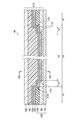
なお、図15、16、及び、図15のXX-XX線における断面を示す図20に示すように、第2の絶縁膜134と第1の絶縁膜80との間に、段差緩和層160を設ける構成とすることが望ましい。段差緩和層160は、第1の絶縁膜80の上面に形成されており、第2の絶縁膜134の下面からその一部がはみ出すように形成されている。この段差緩和層160の存在により、第2の絶縁膜134、第1の絶縁膜80の上面に形成される配線116が、第2の絶縁膜134と第1の絶縁膜80の境界領域において、急な傾斜を持つことを抑制することができ、その結果として、配線116の断線の発生を抑制することができる。なお、この段差緩和層160は、例えばポリシリコン膜などを用いて形成することができる。
ここで、図20に示すように、湾曲領域120において、第1の絶縁膜80を配線116の下方に設けない構成とすることにより、配線116が破壊されるリスクを低減することができる。即ち、一般的に無機絶縁膜は曲げに伴って割れてしまうリスクが高い。従って、湾曲領域120を湾曲させるに際して無機絶縁膜である第1の絶縁膜80が割れてしまうリスクがある。しかし、この図15、16、20に示す実施例によれば、湾曲領域120において、第1の絶縁膜80が配線116の下方に設けられていない構成であるため、湾曲領域120の曲げに伴い第1絶縁膜80が割れてしまうことを抑制することができる。その結果として、第1の絶縁膜80の割れに伴う衝撃により配線116が破壊されるリスクを低減することができる。
なお、本実施形態においては、絶縁壁200が第2の絶縁膜134と一体形成された構成を例に挙げて説明したが、絶縁壁200と第2の絶縁膜134とが別体として構成されていてもよい。ただし、本実施形態に示すように、絶縁壁200と第2の絶縁膜134を同一材料で、一体形成することで、製造コストの低減を図ることができる。
また、絶縁壁200と第2の絶縁膜134とを同一材料にて一体形成することにより、第1の配線116Aと第2の配線116Bとが電気的に接続される可能性を、更に低減することができる。即ち、第1の配線116Aと第2の配線116Bとが電気的に接続されるリスクが最も高いのは、絶縁壁200近傍にまで生じた段差の影響で第1の導体140Aが残存しうる第1の絶縁膜80と第2の絶縁膜134との境界領域であるが、この第1の絶縁膜80と第2の絶縁膜134との境界領域は、第2の絶縁膜134と絶縁壁200との境界領域でもある。従って、第2の絶縁膜134と絶縁壁200とを同一材料にて一体形成しておくことにより、湾曲領域120形成時に加わる応力により、第2の絶縁膜134と絶縁壁200とが断裂してしまう可能性を低減させることができ、その結果として、第1の配線116Aと第2の配線116Bとが電気的に接続される可能性を、更に低減することができるのである。
なお、図17、18に示すように、電位が異なる複数の各信号線116C、116D、116Eの間には、上述した絶縁壁200を設けることにより、信号線116Cと信号線116D、及び信号線116Dと信号線116Eが、ドライエッチング工程において除去しきれなかった第1の導体140A、第2の導体140Bにより、電気的に接続されることを抑制することができるため望ましい。同様に、電位が異なる信号線116Eと電源線116Fとの間にも、上述した絶縁壁200を設けることにより、信号線116Eと電源線116Fとが、第1の導体140A、第2の導体140Bにより、電気的に接続されることを抑制することができるため望ましい。
なお、図17、18に示すように、湾曲領域120の剛性を低減させるべく、電源線116Fに開口部を設けているような場合において、当該開口部形成領域においては、絶縁壁200を設ける必要はない。電源線116Fは開口部の右側と左側とで電位は変わらず、ドライエッチング工程にいて除去しきれなかった第1の導体140A、第2の導体140Bにより電気的に接続されても問題がないためである。また、開口部形成領域において絶縁壁200を設けない構成にすることにより、限られた面積で電源線116Fを形成することができ、表示装置2の小面積化を図ることができる。
また、図19に示すように、各配線116が複数の菱形を組み合わせた形状をしているような場合、各配線116間に設ける絶縁壁200の形状としては、当該菱形の頂点に合わせた湾曲部を有するジグザグ形状とすることが望ましい。このような構成とすることにより、各配線116と絶縁壁200とをより密接して配置することが可能となる。さらに各配線116自身の曲げ耐性も上がることとなる。
なお、図19に示すように、各配線116における菱形形状の内側をエッチング等により導体を除去し開口部を設け、第1の絶縁膜80、絶縁性基材70を露出させているような場合においては、絶縁壁200を設ける必要はない。同一の配線116内において、電位は変わらず、ドライエッチング工程において除去しきれなかった導体140により電気的に接続されても問題がないためである。むしろ、開口部領域において絶縁壁200を設けない構成にすることにより、配線116形状の自由度を高めることができる。また、面積の小さな開口部領域内において絶縁壁200がごみとなって飛び散ることを抑制することができ、その結果として、歩留り等の悪影響となる不具合を回避することができ望ましい。
Claims (19)
- 画素アレイ部を有する表示領域と、前記表示領域の裏面側に設けられ、前記画素アレイ部を駆動する駆動部を有する駆動部形成領域と、前記表示領域と駆動部形成領域とを連結する湾曲領域と、を有する表示パネルを含み、
前記表示パネルは、
前記表示領域から前記駆動部形成領域にまで設けられ、且つ前記湾曲領域において、前記表示領域の膜厚及び前記駆動部形成領域の膜厚よりも薄い第1の膜厚を有する第1の膜厚領域を有し、前記表示領域と前記第1の膜厚領域との間に配置された第1の段差部と、前記駆動部形成領域と前記第1の膜厚領域との間に配置された第2の段差部とを有する絶縁性シートと、
前記絶縁性シートの上方において、前記第1の段差部と、前記第2の段差部とを横切り、且つ前記画素アレイ部と前記駆動部とを電気的に接続する第1の配線、及び第2の配線と、
前記第1の配線と前記第2の配線との間において、前記第1の段差部から前記第2の段差部まで延伸する絶縁壁と、
を含む、表示装置。 - 前記絶縁壁の上面が、前記表示領域、及び前記駆動部形成領域における前記絶縁性シートの上面と連続する、
請求項1に記載の表示装置。 - 前記第1の段差部と前記第2の段差部に配置された第1の導体を含む、
請求項1又は2に記載の表示装置。 - 前記絶縁性シートが、前記第1の膜厚領域の中央側において、前記第1の膜厚よりも薄い第2の膜厚を有する第2の膜厚領域を有し、
前記第1の配線と前記第2の配線の内の少なくとも一方が、前記第1の膜厚領域と前記第2の膜厚領域との間に配置された第3の段差部を横切るよう配置された、
請求項1乃至3のいずれか一つに記載の表示装置。 - 前記第3の段差部に配置された第2の導体を含む、
請求項4に記載の表示装置。 - 前記絶縁性シートは、絶縁性基材と、前記絶縁性基材上に設けられた第1の絶縁膜と、を含み、前記第2の膜厚領域において、前記第1の絶縁膜の少なくとも一部から前記絶縁性基材の上面が露出された、
請求項4又は5に記載の表示装置。 - 前記絶縁性基材はポリイミドからなる、
請求項6に記載の表示装置。 - 前記第1の絶縁膜は酸化シリコン層と窒化シリコン層との積層体からなる、
請求項6に記載の表示装置。 - 前記絶縁性シートは、前記表示領域における前記第1の絶縁膜と前記第1の配線との間、及び前記第1の絶縁膜と前記第2の配線との間に、第2の絶縁膜を更に含む、
請求項6に記載の表示装置。 - 前記第2の絶縁膜と前記第1の絶縁膜との間に、段差緩和層が設けられた、
請求項9に記載の表示装置。 - 前記絶縁壁の少なくとも一部が、前記第2の絶縁膜と同一材料で構成された、
請求項9又は10に記載の表示装置。 - 前記第1の配線と前記第2の配線とは電位が異なる信号線である、
請求項1乃至11のいずれか一つに記載の表示装置。 - 画素アレイ部を有する表示領域と、前記表示領域の裏面側に設けられ、前記画素アレイ部を駆動する駆動部を有する駆動部形成領域と、前記表示領域と駆動部形成領域とを連結する湾曲領域と、を有する表示パネルを含み、
前記表示パネルは、
有機材料で構成された絶縁性基材と、
前記絶縁性基材上に設けられ、無機絶縁材料で構成され、前記表示領域から前記駆動部形成領域にまで設けられ、且つ前記湾曲領域において、前記表示領域の膜厚及び前記駆動部形成領域の膜厚よりも薄い第1の膜厚を有する第1の膜厚領域を有し、前記表示領域と前記第1の膜厚領域との間に配置された第1の段差部と、前記駆動部形成領域と前記第1の膜厚領域との間に配置された第2の段差部とを有する無機絶縁膜と、
前記無機絶縁膜の上方において、前記第1の段差部と、前記第2の段差部とを横切り、且つ前記画素アレイ部と前記駆動部とを電気的に接続する第1の配線、及び第2の配線と、
前記第1の配線と前記第2の配線との間において、前記第1の段差部から前記第2の段差部まで延伸する絶縁壁と、
を含む、表示装置。 - 前記絶縁壁の上面が、前記表示領域、及び前記駆動部形成領域における前記無機絶縁膜の上面と連続する、
請求項13に記載の表示装置。 - 前記第1の段差部と前記第2の段差部に配置された第1の導体を含む、
請求項13又は14に記載の表示装置。 - 前記無機絶縁膜が、前記第1の膜厚領域の中央側において、前記第1の膜厚よりも薄い第2の膜厚を有する第2の膜厚領域を有し、
前記第1の配線と前記第2の配線の内の少なくとも一方が、前記第1の膜厚領域と前記第2の膜厚領域との間に配置された第3の段差部を横切るよう配置された、
請求項13乃至15のいずれか一つに記載の表示装置。 - 前記無機絶縁膜は、前記絶縁性基材と前記第1の配線および第2の配線との間に配置された第1の絶縁膜と、前記第1の絶縁膜と前記第1の配線および第2の配線との間に配置された第2の絶縁膜を含む、
請求項13に記載の表示装置。 - 前記第2の絶縁膜と前記第1の絶縁膜との間に、段差緩和層が設けられた、
請求項17に記載の表示装置。 - 前記絶縁壁の少なくとも一部が、前記第2の絶縁膜と同一材料で構成された、
請求項17又は18に記載の表示装置。
Priority Applications (3)
| Application Number | Priority Date | Filing Date | Title |
|---|---|---|---|
| CN201780084096.6A CN110226192B (zh) | 2017-01-20 | 2017-11-22 | 显示装置 |
| US16/512,646 US10985232B2 (en) | 2017-01-20 | 2019-07-16 | Display device included a folded-back display panel portion for a driver |
| US17/210,680 US11508802B2 (en) | 2017-01-20 | 2021-03-24 | Semiconductor device |
Applications Claiming Priority (2)
| Application Number | Priority Date | Filing Date | Title |
|---|---|---|---|
| JP2017008563A JP6777558B2 (ja) | 2017-01-20 | 2017-01-20 | 表示装置 |
| JP2017-008563 | 2017-01-20 |
Related Child Applications (1)
| Application Number | Title | Priority Date | Filing Date |
|---|---|---|---|
| US16/512,646 Continuation US10985232B2 (en) | 2017-01-20 | 2019-07-16 | Display device included a folded-back display panel portion for a driver |
Publications (1)
| Publication Number | Publication Date |
|---|---|
| WO2018135127A1 true WO2018135127A1 (ja) | 2018-07-26 |
Family
ID=62908724
Family Applications (1)
| Application Number | Title | Priority Date | Filing Date |
|---|---|---|---|
| PCT/JP2017/041959 Ceased WO2018135127A1 (ja) | 2017-01-20 | 2017-11-22 | 表示装置 |
Country Status (4)
| Country | Link |
|---|---|
| US (2) | US10985232B2 (ja) |
| JP (1) | JP6777558B2 (ja) |
| CN (1) | CN110226192B (ja) |
| WO (1) | WO2018135127A1 (ja) |
Cited By (6)
| Publication number | Priority date | Publication date | Assignee | Title |
|---|---|---|---|---|
| WO2020017007A1 (ja) * | 2018-07-19 | 2020-01-23 | シャープ株式会社 | 表示装置およびその製造方法 |
| WO2020044439A1 (ja) * | 2018-08-28 | 2020-03-05 | シャープ株式会社 | 表示装置 |
| WO2020065825A1 (ja) * | 2018-09-27 | 2020-04-02 | シャープ株式会社 | 表示デバイス、表示デバイスの製造方法 |
| WO2020145296A1 (ja) * | 2019-01-09 | 2020-07-16 | 株式会社Joled | 表示パネルおよび表示装置 |
| US20210066440A1 (en) * | 2018-01-31 | 2021-03-04 | Sharp Kabushiki Kaisha | Display device |
| EP3859783A4 (en) * | 2018-09-27 | 2022-06-22 | Boe Technology Group Co., Ltd. | ARRAY SUBSTRATE, DISPLAY PANEL AND DISPLAY DEVICE |
Families Citing this family (8)
| Publication number | Priority date | Publication date | Assignee | Title |
|---|---|---|---|---|
| KR102370450B1 (ko) * | 2017-07-07 | 2022-03-04 | 삼성디스플레이 주식회사 | 표시 장치 |
| KR102426617B1 (ko) * | 2017-10-27 | 2022-07-28 | 엘지디스플레이 주식회사 | 표시장치 및 그의 제조방법 |
| JP7068800B2 (ja) * | 2017-10-30 | 2022-05-17 | 株式会社ジャパンディスプレイ | 表示装置 |
| WO2020148852A1 (ja) * | 2019-01-17 | 2020-07-23 | シャープ株式会社 | 表示装置 |
| CN114600556B (zh) * | 2019-10-21 | 2025-06-03 | 夏普株式会社 | 显示装置 |
| CN111146189A (zh) * | 2019-12-16 | 2020-05-12 | 深圳市华星光电半导体显示技术有限公司 | 一种显示模组及其制备方法及电子装置 |
| KR102842888B1 (ko) * | 2020-12-08 | 2025-08-07 | 주식회사 엘엑스세미콘 | 회로 구동부 및 그를 포함한 표시 장치 |
| US20230180399A1 (en) * | 2021-12-07 | 2023-06-08 | Meta Platforms Technologies, Llc | Design to protect chip-on-flex for dual bending |
Citations (5)
| Publication number | Priority date | Publication date | Assignee | Title |
|---|---|---|---|---|
| JPH02132418A (ja) * | 1988-07-11 | 1990-05-21 | Toshiba Corp | フレキシブル配線基板及びその製造方法及び電子部品 |
| JP2001148547A (ja) * | 1999-11-18 | 2001-05-29 | Sanyo Electric Co Ltd | 電気装置の接続に用いるcof基板 |
| JP2002358026A (ja) * | 2001-03-26 | 2002-12-13 | Sharp Corp | 表示モジュール並びにフレキシブル配線板及びフレキシブル配線板の接続方法 |
| JP2014197181A (ja) * | 2013-03-07 | 2014-10-16 | 株式会社半導体エネルギー研究所 | 表示装置 |
| JP2015121777A (ja) * | 2013-11-20 | 2015-07-02 | 株式会社Joled | 表示装置、およびその製造方法 |
Family Cites Families (12)
| Publication number | Priority date | Publication date | Assignee | Title |
|---|---|---|---|---|
| US9419065B2 (en) | 2012-08-07 | 2016-08-16 | Apple Inc. | Flexible displays |
| US8890408B2 (en) | 2013-01-18 | 2014-11-18 | Nokia Corporation | Method and apparatus for coupling an active display portion and substrate |
| US9740035B2 (en) | 2013-02-15 | 2017-08-22 | Lg Display Co., Ltd. | Flexible organic light emitting display device and method for manufacturing the same |
| US9516743B2 (en) | 2013-02-27 | 2016-12-06 | Apple Inc. | Electronic device with reduced-stress flexible display |
| JP2014206596A (ja) * | 2013-04-11 | 2014-10-30 | 株式会社ジャパンディスプレイ | 液晶表示装置及びその製造方法 |
| KR102018741B1 (ko) | 2013-06-03 | 2019-09-06 | 삼성디스플레이 주식회사 | 커버 윈도우를 구비하는 표시 장치 |
| KR102086644B1 (ko) * | 2013-12-31 | 2020-03-09 | 엘지디스플레이 주식회사 | 플렉서블표시장치 및 이의 제조방법 |
| JP6469427B2 (ja) * | 2014-12-03 | 2019-02-13 | 株式会社ジャパンディスプレイ | 表示装置 |
| US20160172428A1 (en) | 2014-12-11 | 2016-06-16 | Lg Display Co., Ltd. | Flexible display device with corrosion resistant printed circuit film |
| CN104934438A (zh) * | 2015-04-24 | 2015-09-23 | 京东方科技集团股份有限公司 | 一种显示基板及其制作方法、显示装置 |
| JP6762845B2 (ja) * | 2016-10-28 | 2020-09-30 | 株式会社ジャパンディスプレイ | 表示装置及び配線基板 |
| WO2018163337A1 (ja) * | 2017-03-08 | 2018-09-13 | シャープ株式会社 | 可撓性表示パネル、可撓性表示装置及び可撓性表示パネルの製造方法 |
-
2017
- 2017-01-20 JP JP2017008563A patent/JP6777558B2/ja active Active
- 2017-11-22 WO PCT/JP2017/041959 patent/WO2018135127A1/ja not_active Ceased
- 2017-11-22 CN CN201780084096.6A patent/CN110226192B/zh active Active
-
2019
- 2019-07-16 US US16/512,646 patent/US10985232B2/en active Active
-
2021
- 2021-03-24 US US17/210,680 patent/US11508802B2/en active Active
Patent Citations (5)
| Publication number | Priority date | Publication date | Assignee | Title |
|---|---|---|---|---|
| JPH02132418A (ja) * | 1988-07-11 | 1990-05-21 | Toshiba Corp | フレキシブル配線基板及びその製造方法及び電子部品 |
| JP2001148547A (ja) * | 1999-11-18 | 2001-05-29 | Sanyo Electric Co Ltd | 電気装置の接続に用いるcof基板 |
| JP2002358026A (ja) * | 2001-03-26 | 2002-12-13 | Sharp Corp | 表示モジュール並びにフレキシブル配線板及びフレキシブル配線板の接続方法 |
| JP2014197181A (ja) * | 2013-03-07 | 2014-10-16 | 株式会社半導体エネルギー研究所 | 表示装置 |
| JP2015121777A (ja) * | 2013-11-20 | 2015-07-02 | 株式会社Joled | 表示装置、およびその製造方法 |
Cited By (9)
| Publication number | Priority date | Publication date | Assignee | Title |
|---|---|---|---|---|
| US20210066440A1 (en) * | 2018-01-31 | 2021-03-04 | Sharp Kabushiki Kaisha | Display device |
| US11574982B2 (en) * | 2018-01-31 | 2023-02-07 | Sharp Kabushiki Kaisha | Display device |
| WO2020017007A1 (ja) * | 2018-07-19 | 2020-01-23 | シャープ株式会社 | 表示装置およびその製造方法 |
| WO2020044439A1 (ja) * | 2018-08-28 | 2020-03-05 | シャープ株式会社 | 表示装置 |
| CN112585665A (zh) * | 2018-08-28 | 2021-03-30 | 夏普株式会社 | 显示装置 |
| US11889728B2 (en) | 2018-08-28 | 2024-01-30 | Sharp Kabushiki Kaisha | Display device |
| WO2020065825A1 (ja) * | 2018-09-27 | 2020-04-02 | シャープ株式会社 | 表示デバイス、表示デバイスの製造方法 |
| EP3859783A4 (en) * | 2018-09-27 | 2022-06-22 | Boe Technology Group Co., Ltd. | ARRAY SUBSTRATE, DISPLAY PANEL AND DISPLAY DEVICE |
| WO2020145296A1 (ja) * | 2019-01-09 | 2020-07-16 | 株式会社Joled | 表示パネルおよび表示装置 |
Also Published As
| Publication number | Publication date |
|---|---|
| JP6777558B2 (ja) | 2020-10-28 |
| CN110226192A (zh) | 2019-09-10 |
| US10985232B2 (en) | 2021-04-20 |
| US20190341442A1 (en) | 2019-11-07 |
| CN110226192B (zh) | 2021-08-27 |
| US11508802B2 (en) | 2022-11-22 |
| JP2018116224A (ja) | 2018-07-26 |
| US20210210586A1 (en) | 2021-07-08 |
Similar Documents
| Publication | Publication Date | Title |
|---|---|---|
| CN110226192B (zh) | 显示装置 | |
| JP6253541B2 (ja) | 表示装置 | |
| US10573706B2 (en) | Display device | |
| US10720485B2 (en) | Display device having a reduced risk of disconnection of a wiring line included in a curved region | |
| US10134828B2 (en) | Display device and method of manufacturing a display device | |
| JP2020109452A (ja) | 表示装置及び表示装置の製造方法 | |
| WO2019187074A1 (ja) | 表示デバイス | |
| JP2018155999A (ja) | 表示装置 | |
| JP2019003040A (ja) | 表示装置 | |
| CN110476198B (zh) | 显示装置 | |
| JP2008226483A (ja) | 有機el表示装置 | |
| JP2018205486A (ja) | 表示装置および表示装置の製造方法 | |
| WO2018220683A1 (ja) | 表示装置及び表示装置の製造方法 | |
| JP2019016504A (ja) | 表示装置、及び表示装置の製造方法 | |
| JP2019003026A (ja) | 表示装置 | |
| JP6056073B2 (ja) | 表示装置 | |
| JP7246534B2 (ja) | アレイ基板 | |
| JP2019066683A (ja) | 表示装置および表示装置の製造方法 | |
| US20180358423A1 (en) | Display device | |
| JP7220084B2 (ja) | 表示装置 | |
| WO2019102670A1 (ja) | 表示装置 | |
| WO2019187161A1 (ja) | 表示デバイス | |
| JP2018106803A (ja) | 有機el表示装置および有機el表示装置の製造方法 | |
| WO2023223465A1 (ja) | 表示装置およびその製造方法 | |
| JP2007123023A (ja) | 有機el表示装置 |
Legal Events
| Date | Code | Title | Description |
|---|---|---|---|
| 121 | Ep: the epo has been informed by wipo that ep was designated in this application |
Ref document number: 17892776 Country of ref document: EP Kind code of ref document: A1 |
|
| NENP | Non-entry into the national phase |
Ref country code: DE |
|
| 122 | Ep: pct application non-entry in european phase |
Ref document number: 17892776 Country of ref document: EP Kind code of ref document: A1 |