WO2018096977A1 - 導電性フィルム、及び導電性フィルムの製造方法 - Google Patents
導電性フィルム、及び導電性フィルムの製造方法 Download PDFInfo
- Publication number
- WO2018096977A1 WO2018096977A1 PCT/JP2017/040924 JP2017040924W WO2018096977A1 WO 2018096977 A1 WO2018096977 A1 WO 2018096977A1 JP 2017040924 W JP2017040924 W JP 2017040924W WO 2018096977 A1 WO2018096977 A1 WO 2018096977A1
- Authority
- WO
- WIPO (PCT)
- Prior art keywords
- base resin
- resin
- film
- conductive
- layer
- Prior art date
- Legal status (The legal status is an assumption and is not a legal conclusion. Google has not performed a legal analysis and makes no representation as to the accuracy of the status listed.)
- Ceased
Links
Images

Classifications
-
- H—ELECTRICITY
- H01—ELECTRIC ELEMENTS
- H01B—CABLES; CONDUCTORS; INSULATORS; SELECTION OF MATERIALS FOR THEIR CONDUCTIVE, INSULATING OR DIELECTRIC PROPERTIES
- H01B5/00—Non-insulated conductors or conductive bodies characterised by their form
- H01B5/14—Non-insulated conductors or conductive bodies characterised by their form comprising conductive layers or films on insulating-supports
-
- B—PERFORMING OPERATIONS; TRANSPORTING
- B05—SPRAYING OR ATOMISING IN GENERAL; APPLYING FLUENT MATERIALS TO SURFACES, IN GENERAL
- B05D—PROCESSES FOR APPLYING FLUENT MATERIALS TO SURFACES, IN GENERAL
- B05D5/00—Processes for applying liquids or other fluent materials to surfaces to obtain special surface effects, finishes or structures
- B05D5/12—Processes for applying liquids or other fluent materials to surfaces to obtain special surface effects, finishes or structures to obtain a coating with specific electrical properties
-
- B—PERFORMING OPERATIONS; TRANSPORTING
- B05—SPRAYING OR ATOMISING IN GENERAL; APPLYING FLUENT MATERIALS TO SURFACES, IN GENERAL
- B05D—PROCESSES FOR APPLYING FLUENT MATERIALS TO SURFACES, IN GENERAL
- B05D7/00—Processes, other than flocking, specially adapted for applying liquids or other fluent materials to particular surfaces or for applying particular liquids or other fluent materials
- B05D7/24—Processes, other than flocking, specially adapted for applying liquids or other fluent materials to particular surfaces or for applying particular liquids or other fluent materials for applying particular liquids or other fluent materials
-
- B—PERFORMING OPERATIONS; TRANSPORTING
- B32—LAYERED PRODUCTS
- B32B—LAYERED PRODUCTS, i.e. PRODUCTS BUILT-UP OF STRATA OF FLAT OR NON-FLAT, e.g. CELLULAR OR HONEYCOMB, FORM
- B32B27/00—Layered products comprising a layer of synthetic resin
- B32B27/18—Layered products comprising a layer of synthetic resin characterised by the use of special additives
-
- B—PERFORMING OPERATIONS; TRANSPORTING
- B32—LAYERED PRODUCTS
- B32B—LAYERED PRODUCTS, i.e. PRODUCTS BUILT-UP OF STRATA OF FLAT OR NON-FLAT, e.g. CELLULAR OR HONEYCOMB, FORM
- B32B7/00—Layered products characterised by the relation between layers; Layered products characterised by the relative orientation of features between layers, or by the relative values of a measurable parameter between layers, i.e. products comprising layers having different physical, chemical or physicochemical properties; Layered products characterised by the interconnection of layers
- B32B7/02—Physical, chemical or physicochemical properties
-
- C—CHEMISTRY; METALLURGY
- C08—ORGANIC MACROMOLECULAR COMPOUNDS; THEIR PREPARATION OR CHEMICAL WORKING-UP; COMPOSITIONS BASED THEREON
- C08J—WORKING-UP; GENERAL PROCESSES OF COMPOUNDING; AFTER-TREATMENT NOT COVERED BY SUBCLASSES C08B, C08C, C08F, C08G or C08H
- C08J7/00—Chemical treatment or coating of shaped articles made of macromolecular substances
- C08J7/04—Coating
- C08J7/044—Forming conductive coatings; Forming coatings having anti-static properties
-
- H—ELECTRICITY
- H01—ELECTRIC ELEMENTS
- H01B—CABLES; CONDUCTORS; INSULATORS; SELECTION OF MATERIALS FOR THEIR CONDUCTIVE, INSULATING OR DIELECTRIC PROPERTIES
- H01B1/00—Conductors or conductive bodies characterised by the conductive materials; Selection of materials as conductors
- H01B1/14—Conductive material dispersed in non-conductive inorganic material
- H01B1/16—Conductive material dispersed in non-conductive inorganic material the conductive material comprising metals or alloys
-
- H—ELECTRICITY
- H01—ELECTRIC ELEMENTS
- H01B—CABLES; CONDUCTORS; INSULATORS; SELECTION OF MATERIALS FOR THEIR CONDUCTIVE, INSULATING OR DIELECTRIC PROPERTIES
- H01B13/00—Apparatus or processes specially adapted for manufacturing conductors or cables
Definitions
- the present invention relates to a conductive film and a method for producing a conductive film.
- metal nanowires have attracted attention as raw materials for highly transparent and highly conductive thin films that can be substituted for ITO (indium tin oxide) films used for transparent electrodes such as touch panels.
- ITO indium tin oxide
- Such metal nanowires are generally produced by heating a metal compound in the presence of a polyol such as polyvinylpyrrolidone and ethylene glycol (Non-patent Document 1).
- Patent Documents 1 to 3 disclose a transparent conductor in which a conductive layer including a particulate metal rod coating or a metal nanowire is directly formed on a polymer film such as polyester.
- the conductive layer is formed by directly applying a solution in which particulate metal rods or metal nanowires are dispersed on a polymer film such as polyester and then removing the solvent component by drying.
- Patent Document 3 discloses an ink for forming a transparent conductive film, which contains silver nanowires, an aqueous solvent, a cellulose binder resin, and a surfactant.
- Patent Document 4 discloses a silver nanowire ink useful as a material for forming a transparent conductor.
- Patent Document 5 discloses a composition for forming a conductive layer containing metal nanowires, polyvinyl acetamide, and a water / alcohol solvent.
- the conductive layer can have a low resistance.
- a conventional technique there is a problem that it is difficult to improve the cost and transparency because it is difficult to reduce the amount of the conductive material used, and anisotropy is exhibited in the conductivity.
- the rod-shaped metal particles and metal nanowires are used in the coating solution or after the coating.
- An object of the present invention is to provide a conductive film capable of suppressing the amount of metal nanowires used and suppressing variations in surface resistance values in a wide range of surface resistance values. Furthermore, it is providing the suitable manufacturing method of the electroconductive film excellent in productivity.
- a conductive film according to an embodiment of the present invention includes a polymer film, a base resin layer formed on at least one surface of the polymer film, an average diameter of 1 to 100 nm, and an aspect ratio. And a conductive layer formed on the base resin layer including metal nanowires having an average ratio of 100 to 2000 and a binder resin.
- the surface resistance value of the conductive layer is 1.0 ⁇ 10 2 to 1.0 ⁇ 10 6 ⁇ / ⁇ , and the variation of the surface resistance value is 15% or less.
- the method for producing a conductive film according to an embodiment of the present invention includes a step of forming a base resin layer on at least one surface of a polymer film, an average diameter of 1 to 100 nm, and an average aspect ratio of 100 to 2000. Applying a metal nanowire ink containing a metal nanowire, a binder resin, and a solvent on the base resin layer formed on the polymer film and drying the ink.
- Embodiments of the present invention provide a conductive film with a small amount of metal nanowires used and a small variation in surface resistance of 1.0 ⁇ 10 2 to 1.0 ⁇ 10 6 ⁇ / ⁇ and a method for manufacturing the same. can do.
- the conductive film which concerns on embodiment of this invention can be used suitably for the conductive film use for the touch panel and electronic paper which were low cost and excellent in resistance value stability.
- the conductive film 10 includes a polymer film 11, a base resin layer 12, and a conductive layer 13.
- the base resin layer 12 is provided on at least one side of the polymer film 11.
- the conductive layer 13 is formed by applying metal nanowire ink onto the base resin layer 12, that is, the surface opposite to the polymer film 11 and drying.
- the metal nanowire ink includes metal nanowires having an average diameter of 1 to 100 nm and an average aspect ratio of 100 to 2000, a binder resin, and a solvent.
- metal nanowire means a nano-order metal fiber formed in a solid linear shape, that is, a wire shape, and a nano-order metal fiber that is formed in a hollow linear shape, that is, a tube shape, so-called metal nanotubes. And both concepts.
- the wire shape and the tube shape can be collectively referred to as a metal nanofiber. Details of each component will be described below.
- the polymer film 11 is not particularly limited as long as it has sufficient adhesion to the base resin layer 12.
- the polymer film 11 is preferably a polymer film such as polyester (polyethylene terephthalate [PET], polyethylene naphthalate [PEN], etc.), polycarbonate, acrylic resin, cycloolefin resin, polysulfone, polyethersulfone, polyamide, polyimide or the like.
- PET polyethylene terephthalate
- PEN polyethylene naphthalate
- the thickness of the polymer film 11 is not particularly limited and is appropriately selected depending on the application and type, but is usually 25 to 500 ⁇ m, more preferably from the viewpoint of mechanical strength, handling properties, and the like.
- the thickness is 38 to 400 ⁇ m, more preferably 50 to 300 ⁇ m.
- the polymer film 11 includes various additives such as antioxidants, heat stabilizers, weathering stabilizers, ultraviolet absorbers, organic lubricants, pigments, dyes, organic or inorganic fine particles, fillers, nuclei. An agent or the like may be added to such an extent that the characteristics are not deteriorated.
- the polymer film 11 may be used as it is without surface treatment. Further, in order to improve the uniformity and adhesion of the base resin layer 12 formed on the polymer film 11, surface treatment such as corona treatment or plasma treatment is performed on the base resin layer 12 side of the polymer film 11. May be.
- the base resin layer 12 is a resin layer formed on the polymer film 11 serving as a base material.
- the base resin layer 12 plays a role of improving the adhesion between the polymer film 11 and the conductive layer 13, the uniformity of the conductive layer 13 formed on the polymer film 11, and the like.
- the resin used for the base resin layer 12, that is, the base resin may be any resin that can be uniformly coated on the polymer film 11 and exhibits good adhesion to the polymer film 11 and the conductive layer 13.
- the base resin used for the base resin layer 12 can be any resin such as thermoplastic, thermosetting, or ultraviolet curable resin.
- a resin such as a polyester resin, an epoxy resin, an acrylic resin, a urethane resin, a melamine resin, a phenol resin, a polyamide resin, or a urea resin can be used alone or in combination.
- a polyester resin is particularly suitable as the base resin used for the base resin layer 12.
- the base resin When a polyester resin is used as the base resin, it may be modified with other components such as acrylic, and the base resin may have a functional group such as —COOH or —SO 3 Na.
- the base resin preferably contains the same resin as the binder resin used for the conductive layer 13 in order to increase the adhesion with the conductive layer 13 and to increase the uniformity of the thickness and conductivity of the conductive layer 13.
- the fact that the base resin and the binder resin contain the same resin means that the base resin and the binder resin completely contain the same component and the same grade resin.
- the resin is not limited to the one containing the same component / grade resin.
- the base resin may be, for example, an antioxidant, a heat stabilizer, a weather stabilizer, an ultraviolet absorber, an organic lubricant such as natural or petroleum wax, a pigment, a dye, an organic or inorganic fine particle, a filler, and a nucleating agent. Etc. may be added to such an extent that the resin properties and the adhesion with the polymer film and the conductive layer are not deteriorated.
- the thickness of the base resin layer 12 is preferably 0.1 to 10 ⁇ m, more preferably 0.2 to 5 ⁇ m, and still more preferably 0.3 to 3 ⁇ m.
- the thickness of the base resin layer 12 is preferably 0.1 to 10 ⁇ m, more preferably 0.2 to 5 ⁇ m, and still more preferably 0.3 to 3 ⁇ m.
- Formation of the base resin layer 12 on the polymer film 11 can be performed by an arbitrary method such as a wet coating method or a CVD method.
- the wet coating method is preferable.
- the wet coating method is relatively simple because it is a method in which the polymer film 11 is coated with a resin solution of a base resin, and the applied resin solution is dried to form the base resin layer 12. This is because it is easy to obtain a base resin layer 12 that is uniform and exhibits good adhesion to the polymer film 11.
- the resin solution here includes not only a resin in which the resin is dissolved but also a resin in which the resin is dispersed in the solvent as an emulsion.
- the solvent used for the resin solution of the base resin can be appropriately selected in consideration of factors such as the type of base resin used and the drying temperature.
- the base resin layer 12 is formed by coating a resin solution of the base resin on the polymer film 11 by a wet coating method
- a known coating method such as a bar coating method, a reverse coating method, a gravure coating method, or a die coating method is used. Any method of blade coating can be used.
- drying can be performed by arbitrary methods, such as a hot air furnace and a far-infrared furnace.
- an ultraviolet irradiation device can be used in combination with or alone with the drying furnace.
- the conductive layer 13 is obtained by forming a metal nanowire ink on the polymer film 11 on which the base resin layer 12 is formed by coating and drying so as to contact the base resin layer 12.
- the metal nanowire ink contains (A) metal nanowire, (B) a binder resin, and (C) a solvent.
- the conductive layer 13 has a surface resistance value of 1.0 ⁇ 10 2 to 1.0 ⁇ 10 6 ⁇ / ⁇ in which metal nanowires are dispersed in a binder resin, and has a variation in surface resistance value of 15% or less.
- the content of the metal nanowires in the conductive layer 13 is preferably 1.5 to 4.5% in terms of the area occupancy ratio of the metal nanowires with respect to the conductive film 10.
- the favorable electroconductive film 10 can be obtained by making the area occupation rate with respect to the electroconductive film 10 of a metal nanowire 1.5% or more.
- the area occupation ratio of the metal nanowires with respect to the conductive film 10 4.5% or less it is possible to obtain a conductive film with high total light transmittance, low haze, and excellent transparency. That is, by making the area occupancy ratio of the metal nanowires with respect to the conductive film 10 1.5% or more and 4.5% or less, the conductivity and transparency are excellent, and the amount of expensive metal nanowires used is small and economical.
- the electroconductive film 10 excellent also in the property can be obtained.
- the metal nanowire is a linear metal having an outer diameter, that is, a diameter of the order of nanometers, and is a conductive material formed in a wire shape or a tube shape.
- the metal nanowire may have flexibility or rigidity.
- Examples of metal nanowires include, for example, solid silver nanowires and silver nanotubes formed in a porous or non-porous tube shape.
- the outer diameter, that is, the average value of the diameter (hereinafter referred to as the average diameter) of the metal nanowire is 1 to 100 nm, preferably 5 to 100 nm, and more preferably 10 to 100 nm.
- the average value of the major axis length of the metal nanowire (hereinafter referred to as average length) is preferably 1 to 100 ⁇ m, more preferably 1 to 50 ⁇ m, further preferably 2 to 50 ⁇ m, and particularly preferably 5 to 30 ⁇ m.
- the average diameter and the average length satisfy the above ranges, and the average aspect ratio is 100 to 2000, preferably 200 to 1000, more preferably 300 to 1000, and more preferably 300 to 700. More preferably it is.
- the aspect ratio is a value obtained by a / b, where b is the average diameter of the metal nanowires and a is the average length. a and b can be measured using a scanning electron microscope (SEM).
- the metal type of the metal nanowire at least one selected from the group consisting of gold, silver, platinum, copper, nickel, iron, cobalt, zinc, ruthenium, rhodium, palladium, cadmium, osmium, iridium and a combination of these metals Alloy and the like.
- the metal nanowire contains at least one of gold and silver among the metals described above.
- An optimal embodiment includes silver nanowires.
- a known production method can be used.
- silver nanowires can be synthesized by reducing silver nitrate in the presence of polyvinylpyrrolidone using the Poly-ol method (see Chem. Mater., 2002, 14, 4736).
- gold nanowires can be synthesized by reducing chloroauric acid hydrate in the presence of polyvinylpyrrolidone (see J. Am. Chem. Soc., 2007, 129, 1733).
- Gold nanotubes having a porous structure can be synthesized by reducing a chloroauric acid solution using silver nanowires as a template.
- the silver nanowire used as a template is dissolved in a solution by an oxidation-reduction reaction with chloroauric acid, and as a result, a gold nanotube having a porous structure is formed (J. Am. Chem. Soc., 2004, 126, 3892). -3901).
- Binder resin The binder resin used for the metal nanowire ink is for dispersing and fixing the metal nanowire in the conductive layer 13, and any resin such as thermoplastic, thermosetting, or ultraviolet curable resin is used. can do.
- a resin such as a polyester resin, an epoxy resin, an acrylic resin, a urethane resin, a melamine resin, a phenol resin, a polyamide resin, or a urea resin can be used alone or in combination.
- the binder resin used in the metal nanowire ink is used as the base resin used for the base resin layer 12 in order to increase the adhesion with the base resin layer 12 and to increase the uniformity of the thickness and conductivity of the conductive layer 13. It is preferable that the same resin is included.
- the fact that the binder resin and the base resin contain the same resin means that the base resin and the binder resin completely contain the same component and the same grade resin.
- the resin is not limited to the one containing the same component / grade resin.
- the base resin and the binder resin may be of different grades as long as they contain the same component resin.
- the binder resin is particularly preferably a polyester resin.
- a polyester resin as the binder resin, not only can the metal nanowires be uniformly dispersed and fixed in the binder resin layer, that is, the base resin layer 12, but also transparency, solvent resistance, and wear resistance can be easily obtained. It is because it can be given to.
- binder resin those having an ionic functional group such as —COOH and —SO 3 Na can be used. According to this, the solubility and dispersibility of the binder resin in the solvent can be improved, and the dispersibility of the metal nanowires can be improved. Moreover, when using polyester resin as binder resin, you may modify
- Binder resins include, for example, antioxidants, heat stabilizers, weathering stabilizers, UV absorbers, organic lubricants such as natural or petroleum wax, pigments, dyes, organic or inorganic fine particles, fillers, nucleating agents, etc. These additives may be added to such an extent that the properties of the binder resin and the dispersibility of the metal nanowires are not deteriorated.
- the content of the binder resin in the conductive layer 13 is preferably 1000 to 2000 parts by mass, more preferably 1250 to 1750 parts by mass with respect to 100 parts by mass of the metal nanowires in the conductive layer 13.
- the content of the binder resin in the conductive layer 13 is preferably 1000 to 2000 parts by mass, more preferably 1250 to 1750 parts by mass with respect to 100 parts by mass of the metal nanowires in the conductive layer 13.
- (C) Solvent As the solvent contained in the metal nanowire ink, for example, water, an organic solvent, or the like can be used alone or in combination. In this case, as the solvent contained in the metal nanowire ink, any solvent can be used as long as the binder resin can be dissolved or dispersed as an emulsion and the metal nanowires can be dispersed.
- the amount of the solvent to be used is not particularly limited as long as it can provide a uniform conductive layer 13 when the metal nanowire ink is coated on the base resin layer 12 formed on the polymer film 11. In this case, it is preferable to adjust the amount of the solvent so that the solid content of the metal nanowire or binder resin contained in the metal nanowire ink is 0.1 to 10% by mass with respect to the entire metal nanowire ink.
- the solvent a mixed solvent of alcohol and water containing at least one saturated monohydric alcohol having 1 to 3 carbon atoms (methanol, ethanol, 1-propanol and 2-propanol) can be preferably used.
- the solvent is preferably a solvent in which a saturated monohydric alcohol having 1 to 3 carbon atoms is contained in a range of 1 to 50% by mass in the total solvent.
- the metal nanowire ink may contain additives such as surfactants, antioxidants, fillers and the like as long as they do not adversely affect performance such as coating film properties, conductivity, and optical properties.
- a filler such as fumed silica can be used.
- the total amount of these components is preferably within 5 parts by mass with respect to 100 parts by mass of the solid content excluding the solvent.
- the metal nanowire described above, a binder resin, and an additive that can be added as necessary are blended in the above blending ratio (mass%), mixed with a solvent, and further a rotation and revolution stirrer. It is produced by mixing with stirring. As a result, a metal nanowire ink having a viscosity of about 1 to 50 mPa ⁇ s can be obtained.
- the metal nanowire ink is applied onto a polymer film on which a base resin layer is formed so as to be in contact with the base resin layer to form a coating film, and then dried to obtain a target conductive film. it can.
- a known coating method such as a bar coating method, a reverse coating method, a gravure coating method, a die coating method, or a blade coating method can be used.
- drying can be performed by arbitrary methods, such as a hot air furnace and a far-infrared furnace.
- an ultraviolet irradiation device can be used in combination with or alone with the drying furnace.
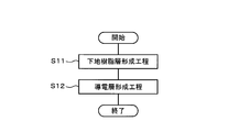
- the manufacturing process of the conductive film 10 includes a base resin layer forming process in step S11 and a conductive layer forming process in step S12.
- a base resin layer forming process is executed in step S11.
- the base resin layer 12 is formed on at least one surface of the polymer film 11 by an arbitrary method such as a wet coating method or a CVD method.
- step S12 a conductive layer forming step is executed.
- the metal nanowire ink described above is applied on the base resin layer 12 formed in step S11, and then the solvent component is removed by drying. Thereby, the conductive layer 13 is formed on the base resin layer 12, and the conductive film 10 is completed.
- the conductive film 10 is formed by forming the conductive layer 13 on the polymer film 11 with the base resin layer 12 interposed therebetween, and the surface resistance value is 1.0 ⁇ 10 2 to 1.0 ⁇ 10.
- the conductive film 10 having 6 ⁇ / ⁇ and having a surface resistance variation of 15% or less can be obtained.
- the conductive film 10 of the present embodiment has a total light transmittance of preferably 80% or more, more preferably 85% or more, and a haze value of preferably 0.1 to 1.5%, more preferably 0.1. ⁇ 1.0%.
- a total light transmittance preferably 80% or more, more preferably 85% or more, and a haze value of preferably 0.1 to 1.5%, more preferably 0.1. ⁇ 1.0%.
- a hard coat may be formed on the conductive layer 13 formed on the base resin layer 12 or on the surface of the polymer film 11 where the conductive layer 13 is not formed.
- a functional layer such as a layer may be formed.
- the shape (length / diameter) of the metal nanowire is 50 nanowire diameters and lengths arbitrarily selected using an ultra-high resolution field emission scanning electron microscope SU8020 (acceleration voltage 3 to 10 kV) manufactured by Hitachi High-Technologies Corporation. The arithmetic average value was obtained.
- silver nanowires were used as metal nanowires.
- an ultraviolet-visible absorption spectrum at 300 to 600 nm was measured using an ultraviolet-visible near-infrared spectrophotometer V-670 manufactured by JASCO Corporation, and the maximum peak value Abs of absorbance at 370 nm to 380 nm based on metal nanowires ( The ratio (Abs ( ⁇ 450) / Abs ( ⁇ max)) between the absorbance value Abs ( ⁇ 450) at a wavelength of 450 nm and the silver spherical particles was determined. Although it depends on the shape of the metal nanowires, this ratio is preferably in the range of 0.1 to 0.5. The smaller this ratio, the smaller the number of spherical particles generated during the synthesis of the metal nanowires. When spherical particles are not present, the value is about 0.1.
- the silver nitrate solution (second solution) prepared above is put in a dropping funnel, and the average supply mole number of silver nitrate is 0.087 mmol / min while maintaining the temperature of the first solution at 150 ° C.
- Silver nanowires were synthesized by dropping the second solution over 2.5 hours.
- the molar ratio calculated from the number of moles of the ionic derivative and the average number of moles of silver nitrate supplied is 0.22.
- the molar ratio of the ionic derivative to the metal salt (metal salt / ionic derivative) was in the range of 0.2 to 6.7. After completion of the dropwise addition, the mixture was further heated and stirred for 1 hour to complete the reaction.
- the reaction mixture was diluted 5 times with water, and silver nanowires were precipitated by applying a centrifugal force at a rotational speed of 6000 rpm for 5 minutes using a centrifuge. Then, after removing the supernatant, the operation of adding water and treating at 6000 rpm for 5 minutes is further performed twice. After washing the polyvinylpyrrolidone (PVP) and the solvent remaining in the system, a predetermined amount of water is added. A silver nanowire dispersion liquid using water as a dispersion medium was obtained.
- PVP polyvinylpyrrolidone
- the diameter and length of 50 silver nanowires arbitrarily selected from the field emission scanning electron microscope (FE-SEM) image by the above method were measured, and the arithmetic mean value thereof was obtained.
- the diameter was 36.3 nm and the average length was 20.5 ⁇ m.
- Abs ( ⁇ 450) / Abs ( ⁇ max) was determined from the ultraviolet-visible absorption spectrum of the obtained silver nanowire, and was 0.21.
- Example 1 As the binder resin, an aqueous polyester resin dispersion having —SO 3 Na groups was used. This polyester aqueous dispersion was prepared using pesresin A-647GEX manufactured by Takamatsu Yushi Co., Ltd. so that the solid content concentration would be 5% by mass. Hereinafter, this polyester aqueous dispersion is referred to as a pesresin aqueous solution.
- Methanol (MeOH) and 2-propanol (IPA) were prepared for mixing with water, which is a dispersion medium of the silver nanowire dispersion liquid, to obtain a water + alcohol mixed dispersion medium.
- the above-mentioned silver nanowire dispersion liquid using water as a dispersion medium and a 5% by mass aqueous solution of the above pesresin were added, various solvents were added, the lid was capped, and then mixed with a mix rotor .
- the mixing amount is such that the amount of the pesresin component supplied from the aqueous solution of pesresin is 0.60% by mass and the amount of metallic silver supplied by the silver nanowires is 0.04% by mass with respect to the total amount of the total mixture. Adjusted.
- a conductive composition having a viscosity of 2.5 mPa ⁇ s, that is, a silver nanowire ink was obtained.
- ⁇ Silver content> From the obtained silver nanowire ink, a sample liquid in which silver nanowires are dispersed is collected, and nitric acid is added to the sample liquid to dissolve the silver nanowire, and an atomic absorption spectrophotometer (produced by Agilent Technologies, Ltd., furnace The amount of silver was measured with an atomic absorption spectrophotometer AA280Z). As a result, the silver content was 0.04% by mass, and a value close to 0.04% by mass, which was the target for ink production, was obtained.
- the resin solution for the base resin an aqueous dispersion of polyester resin having —SO 3 Na groups, that is, the above-mentioned pesresin aqueous solution was used. That is, the resin solution of the base resin was prepared using pesresin A-647GEX manufactured by Takamatsu Yushi Co., Ltd. so that the solid content concentration would be 5% by mass.
- a polymer film substrate with a resin solution of a base resin that is, an aqueous pesresin solution, using a coating machine 70F0 manufactured by Imoto Seisakusho Co., Ltd., and using a bar coater with a wet film thickness of about 10 ⁇ m. It applied to the surface of PET film as.
- a 100 ⁇ m-thick film of Cosmo Shine A4100 manufactured by Toyobo Co., Ltd. was used.
- the surface of the PET film is an easy adhesion surface.
- the size of the PET film is 21 cm ⁇ 30 cm. Then, it was dried at 100 ° C. for 1 minute by a hot air dryer (ETAC HS350 manufactured by Enomoto Kasei Co., Ltd.) to form a PET film with a base resin layer.
- the results are shown in Table 1.
- the area occupied by the silver nanowire (AgNW) of the obtained conductive film is 4.34%
- the surface resistance value is 1.0 ⁇ 10 3 ⁇ / ⁇
- the variation of the surface resistance value is as small as 10%. It was confirmed that the film was a conductive film having uniform conductivity. Further, the total light transmittance was as high as 90.9%, the haze was as small as 0.79%, and it was confirmed that it was extremely excellent in transparency.
- Example 2 The difference from Example 1 is that the silver nanowire ink was applied so that the wet film thickness was about 10 ⁇ m. Except for this point, the same procedure as in Example 1 was performed. The results are shown in Table 1.
- the obtained conductive film has an area occupied by silver nanowires (AgNW) of 3.75%, a surface resistance value of 1.8 ⁇ 10 3 ⁇ / ⁇ , and a variation of the surface resistance value is as small as 7%. It was confirmed that the film was a conductive film having uniform conductivity. Moreover, the total light transmittance was as high as 91.2%, the haze was as small as 0.48%, and it was confirmed that it was extremely excellent in transparency.
- AgNW silver nanowires
- Example 3 The difference from Example 1 is that a silver nanowire ink of an aqueous solvent was used. Except for this point, the same procedure as in Example 1 was performed. The results are shown in Table 1. Compared with Example 1 using a mixed solvent of water and alcohol, the variation in the surface resistance value was slightly large at 15%, but it was at a level that would not interfere with use.
- Example 4 The difference from Example 1 is that the surface on which the base resin layer is provided is subjected to plasma treatment on the PET film before the base resin layer is formed.
- the plasma treatment was performed for 20 seconds at an output of 1 kW in a nitrogen gas atmosphere using a plasma treatment apparatus (AP-T03 manufactured by Sekisui Chemical Co., Ltd.).
- the same procedure as in Example 1 was performed except that plasma treatment was performed.
- the results are shown in Table 1.
- the obtained conductive film has an area occupied by silver nanowires (AgNW) of 4.15%, a surface resistance value of 1.3 ⁇ 10 3 ⁇ / ⁇ , and a variation of the surface resistance value is as small as 11%. It was confirmed that the film was a conductive film having uniform conductivity. Moreover, the total light transmittance was as high as 91.3%, the haze was as small as 0.69%, and it was confirmed that it was extremely excellent in transparency.
- Example 5 The difference from Example 1 is that the polymer film substrate is different and that the polymer film substrate was subjected to plasma treatment in the same manner as Example 4.
- a cycloolefin copolymer (COP) film was used instead of the PET film.
- the COP film is a ZEONOR film ZF14 manufactured by ZEON Corporation and has a thickness of 100 ⁇ m.
- the plasma processing apparatus and conditions used for the plasma processing are the same as in the fourth embodiment. The same procedure as in the first example was performed except that the polymer film substrate was different and that the polymer film substrate was subjected to plasma treatment in the same manner as in Example 4.
- the results are shown in Table 1.
- the obtained conductive film has an area occupied by silver nanowires (AgNW) of 4.23%, a surface resistance value of 1.1 ⁇ 10 3 ⁇ / ⁇ , and a variation of the surface resistance value is as small as 11%. It was confirmed that the film was a conductive film having uniform conductivity. Moreover, the total light transmittance was as high as 91.3%, the haze was as small as 0.67%, and it was confirmed that it was extremely excellent in transparency.
- Comparative Example 1 The difference from Example 1 is that the silver nanowire ink was directly coated on the PET film without forming the base resin layer using the binder resin. Except for this point, the same procedure as in Example 1 was performed. The results are shown in Table 1. Unlike Example 1, it is difficult to form a conductive layer uniformly, so that the surface resistance value is as high as 2.4 ⁇ 10 6 ⁇ / ⁇ , and the variation in surface resistance value is 79. % And the conductivity was confirmed to be non-uniform.
- Comparative Example 2 The difference from Example 1 is that, as a base treatment, only plasma treatment was performed under the same conditions as in Example 4 using a plasma treatment apparatus (AP-T03 manufactured by Sekisui Chemical Co., Ltd.) instead of forming a base resin layer. The conductive layer is formed without forming the base resin layer. Except for this point, the same procedure as in Example 1 was performed. The results are shown in Table 1. By performing the plasma treatment, the surface resistance value became 1.2 ⁇ 10 3 ⁇ / ⁇ , but the variation in the surface resistance value was still as large as 38%, which was not practical.
- a plasma treatment apparatus API-T03 manufactured by Sekisui Chemical Co., Ltd.
- Comparative Example 3 The difference from Example 1 is that a PET film having an acrylic resin hard coat layer was used as the polymer film substrate, and the base resin layer was not formed.
- OPTERIA H522-125 manufactured by Lintec Corporation and a thickness of 125 ⁇ m were used as the PET film.
- Other points were the same as in Example 1. In this case, when silver nanowire ink was applied, ink repelling occurred and it was difficult to form a uniform coating film.
Landscapes
- Engineering & Computer Science (AREA)
- Chemical & Material Sciences (AREA)
- Manufacturing & Machinery (AREA)
- Wood Science & Technology (AREA)
- Life Sciences & Earth Sciences (AREA)
- Chemical Kinetics & Catalysis (AREA)
- Inorganic Chemistry (AREA)
- Health & Medical Sciences (AREA)
- Dispersion Chemistry (AREA)
- Medicinal Chemistry (AREA)
- Polymers & Plastics (AREA)
- Organic Chemistry (AREA)
- Non-Insulated Conductors (AREA)
- Laminated Bodies (AREA)
- Application Of Or Painting With Fluid Materials (AREA)
- Manufacturing Of Electric Cables (AREA)
Abstract
導電性フィルムは、高分子フィルムと、高分子フィルムの少なくとも片面に形成された下地樹脂層と、平均径が1~100nmで且つアスペクト比の平均が100~2000である金属ナノワイヤとバインダー樹脂とを含んで下地樹脂層の上に形成された導電層と、を備える。導電層の表面抵抗値は1.0×10²~1.0×10⁶Ω/□であり、且つ表面抵抗値のばらつきが15%以下である。
Description
本発明は、導電性フィルム、及び導電性フィルムの製造方法に関する。
タッチパネル等の透明電極に使用されるITO(酸化インジウムスズ)膜の代替となる高透明性・高導電性薄膜の原料として、金属ナノワイヤが近年注目されている。かかる金属ナノワイヤは、一般に、ポリビニルピロリドンとエチレングリコール等のポリオールの存在下に金属化合物を加熱することによって製造されている(非特許文献1)。
特許文献1~3には、粒子状金属ロッド塗膜や金属ナノワイヤを含む導電層が、ポリエステル等の高分子フィルム上に直接形成された透明導電体などが開示されている。この場合、導電層は、粒子状金属ロッドや金属ナノワイヤが分散された溶液を、ポリエステル等の高分子フィルム上に直接塗布した後、溶剤成分を乾燥除去することで形成される。
また、特許文献3には、銀ナノワイヤと水性溶媒とセルロース系バインダー樹脂と界面活性剤とを含む、透明導電膜形成用のインクが開示されている。特許文献4には、透明導電体を形成する材料などとして有用な銀ナノワイヤインクが開示されている。特許文献5には、金属ナノワイヤ、ポリビニルアセトアミド、水/アルコール溶媒を含む導電層形成用の組成物が開示されている。
Ducamp-Sanguesa, et al., J. Solid State Chem.,1992, 100, 272
例えば特許文献1~3に示す従来技術によれば、導電層を低抵抗のものにすることが可能と考えられる。しかし、このような従来技術では、導電材料の使用量低減が困難なためコスト面や透明性の改善が困難であったり、導電性に異方性が発現したりする問題がある。また、特許文献1~5に示す従来技術のように、ロッド状金属粒子や金属ナノワイヤを含む希釈塗布液を塗布するものにおいては、ロッド状金属粒子や金属ナノワイヤが塗布液中や塗布後の溶媒乾燥工程において凝集してしまい、その結果、表面抵抗値のばらつきが生じてしまう問題がある。
本発明の目的は、金属ナノワイヤの使用量を抑え、幅広い表面抵抗値領域で表面抵抗値のバラツキを抑制することができる導電性フィルムを提供することにある。さらには、生産性に優れた導電性フィルムの好適な製造方法を提供することにある。
上記目的を達成するために、本発明の実施形態に係る導電性フィルムは、高分子フィルムと、前記高分子フィルムの少なくとも片面に形成された下地樹脂層と、平均径が1~100nmで且つアスペクト比の平均が100~2000である金属ナノワイヤとバインダー樹脂とを含んで前記下地樹脂層の上に形成された導電層と、を備える。前記導電層の表面抵抗値は1.0×10²~1.0×10⁶Ω/□であり、且つ前記表面抵抗値のばらつきが15%以下である。
また、本発明の実施形態に係る導電性フィルムの製造方法は、高分子フィルムの少なくとも片面に下地樹脂層を形成する工程と、平均径が1~100nmで且つアスペクト比の平均が100~2000である金属ナノワイヤと、バインダー樹脂と、溶剤と、を含む金属ナノワイヤインクを、前記高分子フィルムに形成された前記下地樹脂層上に塗布し乾燥させる工程と、を備える。
本発明の実施形態によれば金属ナノワイヤの使用量が少なく、且つ表面抵抗値が1.0×10²~1.0×10⁶Ω/□のばらつきが少ない導電性フィルム及びその製造方法を提供することができる。また、本発明の実施形態に係る導電性フィルムは、低コスト且つ抵抗値安定性に優れたタッチパネルや電子ペーパー向けの導電性フィルム用途に好適に用いることができる。
以下、本発明の実施形態について、図1、2を参照して説明する。
図1に示すように、実施形態の導電性フィルム10は、高分子フィルム11と、下地樹脂層12と、導電層13と、を含んで構成されている。下地樹脂層12は、高分子フィルム11の少なくとも片面に設けられている。導電層13は、金属ナノワイヤインクを、下地樹脂層12上つまり高分子フィルム11とは反対側の面に塗布し乾燥させることで形成されている。金属ナノワイヤインクは、平均径が1~100nmで且つアスペクト比の平均が100~2000である金属ナノワイヤと、バインダー樹脂と、溶剤と、を含んでいる。
図1に示すように、実施形態の導電性フィルム10は、高分子フィルム11と、下地樹脂層12と、導電層13と、を含んで構成されている。下地樹脂層12は、高分子フィルム11の少なくとも片面に設けられている。導電層13は、金属ナノワイヤインクを、下地樹脂層12上つまり高分子フィルム11とは反対側の面に塗布し乾燥させることで形成されている。金属ナノワイヤインクは、平均径が1~100nmで且つアスペクト比の平均が100~2000である金属ナノワイヤと、バインダー樹脂と、溶剤と、を含んでいる。
なお、図1において、高分子フィルム11、下地樹脂層12、及び導電層13の厚みは、理解を容易にするため表現上誇張して描かれており、実際のものとは異なる。また、本願明細書において「金属ナノワイヤ」は、中実の線状つまりワイヤ状に形成されたナノオーダーの金属繊維と、中空の線状つまりチューブ状に形成されたナノオーダーの金属繊維いわゆる金属ナノチューブと、の両方の概念を含む。この場合、ワイヤ状及びチューブ状のものを総称して、金属ナノ繊維と称することもできる。
以下、各構成について詳細を説明する。
以下、各構成について詳細を説明する。
(1)高分子フィルム
高分子フィルム11は、下地樹脂層12と十分な密着性を有するものであれば特に限定されない。高分子フィルム11は、例えばポリエステル(ポリエチレンテレフタレート[PET]、ポリエチレンナフタレート[PEN]等)、ポリカーボネート、アクリル樹脂、シクロオレフィン樹脂、ポリスルフォン、ポリエーテルスルフォン、ポリアミド、ポリイミド等の高分子フィルムを好適に使用することができる。ポリエステル(ポリエチレンテレフタレート[PET]フィルム、ポリエチレンナフタレート[PEN]フィルム等)、ポリカーボネート、アクリル樹脂、シクロオレフィン樹脂の何れかの高分子フィルムを用いることで、透明性に優れた導電性フィルム10を得ることができる。
高分子フィルム11は、下地樹脂層12と十分な密着性を有するものであれば特に限定されない。高分子フィルム11は、例えばポリエステル(ポリエチレンテレフタレート[PET]、ポリエチレンナフタレート[PEN]等)、ポリカーボネート、アクリル樹脂、シクロオレフィン樹脂、ポリスルフォン、ポリエーテルスルフォン、ポリアミド、ポリイミド等の高分子フィルムを好適に使用することができる。ポリエステル(ポリエチレンテレフタレート[PET]フィルム、ポリエチレンナフタレート[PEN]フィルム等)、ポリカーボネート、アクリル樹脂、シクロオレフィン樹脂の何れかの高分子フィルムを用いることで、透明性に優れた導電性フィルム10を得ることができる。
また、高分子フィルム11の厚みは、特に限定されるものではなく、用途や種類に応じて適宜選択されるが、機械的強度、ハンドリング性などの点から、通常は25~500μm、より好ましくは38~400μm、さらに好ましくは50~300μmである。また、高分子フィルム11には、各種添加剤、例えば、酸化防止剤、耐熱安定剤、耐候安定剤、紫外線吸収剤、有機系易滑剤、顔料、染料、有機又は無機の微粒子、充填剤、核剤などがその特性を悪化させない程度に添加されていてもよい。
高分子フィルム11は、表面処理を行うことなくそのまま使用しても良い。また、高分子フィルム11上に形成する下地樹脂層12の均一性や密着性を高めるために、高分子フィルム11の下地樹脂層12側に対して、コロナ処理やプラズマ処理等の表面処理を行っても良い。
(2)下地樹脂層
下地樹脂層12は、基材となる高分子フィルム11上に形成される樹脂層である。下地樹脂層12は、高分子フィルム11と導電層13との密着性や、高分子フィルム11上に形成される導電層13の均一性等を高める役割を果たす。下地樹脂層12に使用する樹脂つまり下地樹脂としては、高分子フィルム11上に均一に塗膜することが可能で、高分子フィルム11及び導電層13と良好な密着性を示す樹脂であれば良い。この場合、下地樹脂層12に使用する下地樹脂は、熱可塑性、熱硬化性、あるいは紫外線硬化性樹脂などの任意の樹脂が使用できる。
下地樹脂層12は、基材となる高分子フィルム11上に形成される樹脂層である。下地樹脂層12は、高分子フィルム11と導電層13との密着性や、高分子フィルム11上に形成される導電層13の均一性等を高める役割を果たす。下地樹脂層12に使用する樹脂つまり下地樹脂としては、高分子フィルム11上に均一に塗膜することが可能で、高分子フィルム11及び導電層13と良好な密着性を示す樹脂であれば良い。この場合、下地樹脂層12に使用する下地樹脂は、熱可塑性、熱硬化性、あるいは紫外線硬化性樹脂などの任意の樹脂が使用できる。
下地樹脂は、例えば、ポリエステル樹脂、エポキシ樹脂、アクリル樹脂、ウレタン樹脂、メラミン樹脂、フェノール樹脂、ポリアミド樹脂、尿素樹脂等の樹脂を単独もしくは混合して使用することができる。この場合、特にポリエステル樹脂が、下地樹脂層12に使用する下地樹脂として好適である。
また、ポリエステル樹脂を下地樹脂として用いる場合、アクリル等他の成分で変性されていても良く、下地樹脂は、-COOHや-SO3Naなどの官能基を有していても良い。そして、導電層13との密着力を高めるとともに、導電層13の厚みや導電率の均一性を高めるために、下地樹脂は導電層13に使用されるバインダー樹脂と同じ樹脂を含むことが好ましい。この場合、下地樹脂とバインダー樹脂とが同じ樹脂を含むとは、下地樹脂とバインダー樹脂とが完全に同一成分・同一グレードの樹脂を含む概念を意味することは勿論であるが、下地樹脂とバインダー樹脂とが完全に同一成分・同一グレードの樹脂を含んでいるものに限られない。
すなわち、この場合、下地樹脂層12と導電層13との何れもが、-SO3H若しくはその金属塩、-COOH、-OH、-NH2から選択される何れかの親水基を有する樹脂成分を含むことが好ましく、-SO3H若しくはその金属塩又は-COOHの何れかの親水基を有する樹脂で構成されていることがより好ましい。更には、下地樹脂層12及び導電層13の何れもが、上述した親水基のうち同一の親水基を有する樹脂で構成されていることがより好ましい。
また、下地樹脂は、例えば、酸化防止剤、耐熱安定剤、耐候安定剤、紫外線吸収剤、天然または石油ワックス等の有機系易滑剤、顔料、染料、有機または無機の微粒子、充填剤、核剤などがその樹脂特性や、高分子フィルム及び導電層との密着性を悪化させない程度に添加されていてもよい。
下地樹脂層12の厚みは、好ましくは0.1~10μmであり、より好ましくは0.2~5μmであり、さらに好ましくは0.3~3μmである。下地樹脂層12の厚みを0.1μm以上とすることで、均一で塗膜むらのない下地樹脂層12を形成することができる。更に、下地樹脂層12の厚みを10μm以下とすることで、透明性や機械特性に優れた導電性フィルム10を生産性よく製造することができる。
高分子フィルム11への下地樹脂層12の形成は、ウェットコーティング法、CVD法等任意の方法で行うことができる。この場合、ウェットコーティング法が好ましい。ウェットコーティング法は、高分子フィルム11に下地樹脂の樹脂溶液を塗膜し、その塗布した樹脂溶液を乾燥させて下地樹脂層12を形成する方法であることから、比較的簡便であり、また、均一で且つ高分子フィルム11と良好な密着力を示す下地樹脂層12を得易いからである。
なお、ここでいう樹脂溶液とは、樹脂が溶剤に溶解しているものだけではなく、エマルションとして樹脂が溶剤中に分散しているものも含む。下地樹脂の樹脂溶液に使用する溶剤は、使用する下地樹脂の種類や乾燥温度等の因子を考慮して、適宜選択することができる。
ウェットコーティング法で、下地樹脂の樹脂溶液を高分子フィルム11上に塗膜して下地樹脂層12を形成する場合、公知のコーティング方式、例えばバーコート法、リバースコート法、グラビアコート法、ダイコート法、ブレードコート法の任意の方式を用いることができる。また、乾燥は、熱風炉、遠赤外炉など、任意の方式で行うことができる。下地樹脂として紫外線硬化性樹脂を用いる場合には、上記乾燥炉と併用または単独で、紫外線照射装置を使用することも可能である。
(3)導電層
導電層13は、金属ナノワイヤインクを、下地樹脂層12が形成された高分子フィルム11上に下地樹脂層12に接するように塗膜・乾燥して形成することで得られる。金属ナノワイヤインクは、(A)金属ナノワイヤ、(B)バインダー樹脂、及び(C)溶剤を含む。導電層13は、バインダー樹脂中に金属ナノワイヤが分散された表面抵抗値が1.0×10²~1.0×10⁶Ω/□であり、表面抵抗値のばらつきが15%以下の導電性フィルムを与える導電性の層である。
導電層13は、金属ナノワイヤインクを、下地樹脂層12が形成された高分子フィルム11上に下地樹脂層12に接するように塗膜・乾燥して形成することで得られる。金属ナノワイヤインクは、(A)金属ナノワイヤ、(B)バインダー樹脂、及び(C)溶剤を含む。導電層13は、バインダー樹脂中に金属ナノワイヤが分散された表面抵抗値が1.0×10²~1.0×10⁶Ω/□であり、表面抵抗値のばらつきが15%以下の導電性フィルムを与える導電性の層である。
導電層13における金属ナノワイヤの含有量は、導電性フィルム10に対する金属ナノワイヤの面積占有率で、1.5~4.5%であることが好ましい。この場合、金属ナノワイヤの導電性フィルム10に対する面積占有率を1.5%以上とすることで、良好な導電性フィルム10を得ることができる。また、金属ナノワイヤの導電性フィルム10に対する面積占有率を4.5%以下とすることで、全光線透過率が高く、ヘイズの小さい、透明性に優れた導電性フィルムを得ることができる。すなわち、金属ナノワイヤの導電性フィルム10に対する面積占有率を1.5%以上で且つ4.5%以下とすることで、導電性及び透明性に優れると共に、高価な金属ナノワイヤの使用量が少なく経済性にも優れた導電性フィルム10を得ることができる。
(A)金属ナノワイヤ
金属ナノワイヤは、外径つまり直径がナノメーターオーダーのサイズの線状の金属であり、ワイヤ形状又はチューブ形状に形成された導電性材料である。金属ナノワイヤは、ワイヤ形状又はチューブ形状のいずれか一方のみを用いることもできるし、両者を併用することもできる。金属ナノワイヤは、柔軟性を有していても良いし、剛性を有していても良い。金属ナノワイヤの一例としては、例えば中実な銀ナノワイヤや、ポーラス又はノンポーラスのチューブ状に形成された銀ナノチューブがある。
金属ナノワイヤは、外径つまり直径がナノメーターオーダーのサイズの線状の金属であり、ワイヤ形状又はチューブ形状に形成された導電性材料である。金属ナノワイヤは、ワイヤ形状又はチューブ形状のいずれか一方のみを用いることもできるし、両者を併用することもできる。金属ナノワイヤは、柔軟性を有していても良いし、剛性を有していても良い。金属ナノワイヤの一例としては、例えば中実な銀ナノワイヤや、ポーラス又はノンポーラスのチューブ状に形成された銀ナノチューブがある。
金属ナノワイヤの外径つまり直径の平均値(以下、平均径と称する)は、1~100nmであり、5~100nmが好ましく、10~100nmがより好ましい。また、金属ナノワイヤの長軸の長さの平均値(以下、平均長と称する)は、1~100μmが好ましく、1~50μmがより好ましく、2~50μmがさらに好ましく、5~30μmが特に好ましい。
金属ナノワイヤは、平均径および平均長が上記範囲を満たすとともに、アスペクト比の平均が100~2000であり、200~1000であることが好ましく、300~1000であることがより好ましく、300~700であることがさらに好ましい。ここで、アスペクト比は、金属ナノワイヤの平均径をbとし、平均長をaとした場合、a/bで求められる値である。a及びbは、走査型電子顕微鏡(SEM)を用いて測定できる。
金属ナノワイヤの金属の種類としては、金、銀、白金、銅、ニッケル、鉄、コバルト、亜鉛、ルテニウム、ロジウム、パラジウム、カドミウム、オスミウム、イリジウムからなる群から選ばれる少なくとも1種およびこれら金属を組み合わせた合金等が挙げられる。低い表面抵抗かつ高い全光線透過率を有する透明導電膜を得るためには、金、銀および銅のいずれかを少なくとも1種含むことが好ましい。これらの金属は導電性が高いため、一定の表面抵抗を得る際に、面に占める金属の密度を減らすことができるので、高い全光線透過率を実現できる。
金属ナノワイヤは、上述した金属の中でも、金または銀の少なくとも1種を含むことがより好ましい。最適な態様としては、銀のナノワイヤが挙げられる。
金属ナノワイヤの製造方法としては、公知の製造方法を用いることができる。例えば、銀ナノワイヤは、ポリオール(Poly-ol)法を用いて、ポリビニルピロリドン存在下で硝酸銀を還元することによって合成することができる(Chem.Mater.,2002,14,4736参照)。金ナノワイヤも同様に、ポリビニルピロリドン存在下で塩化金酸水和物を還元することによって合成することができる(J.Am.Chem.Soc.,2007,129,1733参照)。
銀ナノワイヤの大規模な合成および精製の技術に関しては国際公開公報WO2008/073143パンフレットと国際公開第2008/046058号パンフレットに詳細な記述がある。ポーラス構造を有する金ナノチューブは、銀ナノワイヤを鋳型にして、塩化金酸溶液を還元することにより合成することができる。ここで、鋳型に用いた銀ナノワイヤは塩化金酸との酸化還元反応により溶液中に溶け出し、結果としてポーラス構造を有する金ナノチューブができる(J.Am.Chem.Soc.,2004,126,3892-3901参照)。
(B)バインダー樹脂
金属ナノワイヤインクに用いるバインダー樹脂は、導電層13中に金属ナノワイヤを分散・固定化させるものであり、熱可塑性、熱硬化性、あるいは紫外線硬化性樹脂などの任意の樹脂を使用することができる。バインダー樹脂として、例えばポリエステル樹脂、エポキシ樹脂、アクリル樹脂、ウレタン樹脂、メラミン樹脂、フェノール樹脂、ポリアミド樹脂、尿素樹脂等の樹脂を単独もしくは混合して使用することができる。
金属ナノワイヤインクに用いるバインダー樹脂は、導電層13中に金属ナノワイヤを分散・固定化させるものであり、熱可塑性、熱硬化性、あるいは紫外線硬化性樹脂などの任意の樹脂を使用することができる。バインダー樹脂として、例えばポリエステル樹脂、エポキシ樹脂、アクリル樹脂、ウレタン樹脂、メラミン樹脂、フェノール樹脂、ポリアミド樹脂、尿素樹脂等の樹脂を単独もしくは混合して使用することができる。
この場合、下地樹脂層12との密着力を高めるとともに、導電層13の厚みや導電率の均一性を高めるために、金属ナノワイヤインクに用いられるバインダー樹脂は、下地樹脂層12に用いられる下地樹脂と同じ樹脂を含むことが好ましい。この場合、バインダー樹脂と下地樹脂とが同じ樹脂を含むとは、下地樹脂とバインダー樹脂とが完全に同一成分・同一グレードの樹脂を含む概念を意味することは勿論であるが、下地樹脂とバインダー樹脂とが完全に同一成分・同一グレードの樹脂を含んでいるものに限られない。例えば、下地樹脂とバインダー樹脂とが同一成分の樹脂を含んでいれば、異なるグレードのものであってもよい。
バインダー樹脂としては、特にポリエステル樹脂であることが好ましい。この場合、バインダー樹脂としてポリエステル樹脂を用いることで、金属ナノワイヤをバインダー樹脂層つまり下地樹脂層12へ均一に分散、固定化させることができるだけでなく、透明性や耐溶剤性、耐摩耗性を容易に付与できるためである。
また、バインダー樹脂には、-COOHや-SO3Naなどのイオン性の官能基を有するものを使用できる。これによれば、バインダー樹脂の溶剤への溶解性や分散性が高まるとともに、金属ナノワイヤの分散性を向上させることができる。また、バインダー樹脂としてポリエステル樹脂を用いる場合、アクリル等他の成分で変性されていても良い。そして、下地樹脂層12に対する導電層13の密着力を高めるとともに、導電層13の厚みや導電率の均一性を高めるために、バインダー樹脂は下地樹脂と同じ樹脂成分を含むことが好ましい。バインダー樹脂には、例えば、酸化防止剤、耐熱安定剤、耐候安定剤、紫外線吸収剤、天然または石油ワックス等の有機系易滑剤、顔料、染料、有機または無機の微粒子、充填剤、核剤などの添加剤を、バインダー樹脂の特性、金属ナノワイヤの分散性を悪化させない程度に添加されてもよい。
導電層13におけるバインダー樹脂の含有量は、導電層13中の金属ナノワイヤ100質量部に対して1000~2000質量部であることが好ましく、より好ましくは1250~1750質量部である。導電層13におけるバインダー樹脂の含有量を1000質量部以上とすることで、均一な塗膜の形成ができ、またバインダー樹脂の各種特性や効果を導電性フィルムへ付与することができる。また、導電層13におけるバインダー樹脂を2000質量部以下とすることにより、金属ナノワイヤの導電性を十分に発現させることができる。
(C)溶剤
金属ナノワイヤインクに含まれる溶剤としては、例えば水や有機溶剤などを単独あるいは複数種を混合して用いることができる。この場合、金属ナノワイヤインクに含まれる溶剤は、バインダー樹脂を溶解またはエマルションとして分散させ、金属ナノワイヤを分散させることができれば、任意の溶剤を用いることができる。使用する溶剤の量は、高分子フィルム11に形成された下地樹脂層12上に金属ナノワイヤインクを塗膜した際に均一な導電層13を与えることができる量であれば、特に制約はない。この場合、金属ナノワイヤインクに含有される金属ナノワイヤやバインダー樹脂等の固形分が、金属ナノワイヤインク全体に対して0.1~10質量%になるように、溶剤の量を調整することが好ましい。
金属ナノワイヤインクに含まれる溶剤としては、例えば水や有機溶剤などを単独あるいは複数種を混合して用いることができる。この場合、金属ナノワイヤインクに含まれる溶剤は、バインダー樹脂を溶解またはエマルションとして分散させ、金属ナノワイヤを分散させることができれば、任意の溶剤を用いることができる。使用する溶剤の量は、高分子フィルム11に形成された下地樹脂層12上に金属ナノワイヤインクを塗膜した際に均一な導電層13を与えることができる量であれば、特に制約はない。この場合、金属ナノワイヤインクに含有される金属ナノワイヤやバインダー樹脂等の固形分が、金属ナノワイヤインク全体に対して0.1~10質量%になるように、溶剤の量を調整することが好ましい。
また、溶剤は、炭素原子数が1~3の飽和一価アルコール(メタノール、エタノール、1-プロパノールおよび2-プロパノール)を少なくとも1種含んだアルコールと水との混合溶剤を好適に用いることができる。この場合、溶剤は、炭素原子数が1~3の飽和一価アルコールが全溶剤中の1~50質量%の範囲で含まれたものであることが好ましい。炭素原子数が1~3の飽和一価アルコールを含むことにより、乾燥が容易となり均一な塗膜の形成ができる。
金属ナノワイヤインクには、その塗膜特性、導電性、光学特性等の性能に悪影響を及ぼさない限りにおいて、界面活性剤、酸化防止剤、フィラー、等の添加剤を含有しても良い。組成物の粘性を調整するためにヒュームドシリカ等のフィラーを用いることができる。これらの配合量はトータルで、溶剤を除いた固形分100質量部に対して5質量部以内とすることが好ましい。
実施形態にかかる金属ナノワイヤインクは、以上に述べた金属ナノワイヤ、バインダー樹脂、必要に応じて添加することができる添加剤を上記配合比(質量%)で配合して溶剤と混ぜ、更に自転公転攪拌機等で攪拌して混合することにより製造する。これにより粘度が1~50mPa・s程度の金属ナノワイヤインクが得られる。
上記金属ナノワイヤインクを、下地樹脂層が形成された高分子フィルム上に、下地樹脂層に接するように塗布して塗膜を形成し、乾燥することで、目的とする導電性フィルムを得ることができる。
金属ナノワイヤインクの塗膜は、公知の塗布方式、例えばバーコート法、リバースコート法、グラビアコート法、ダイコート法、ブレードコート法の任意の方式を用いることができる。また、乾燥は、熱風炉、遠赤外炉など、任意の方式で行うことができる。下地樹脂として紫外線硬化性樹脂を用いる場合には、上記乾燥炉と併用または単独で、紫外線照射装置を使用することも可能である。
<製造工程>
本実施形態の導電性フィルム10の製造方法の一例について、図2を参照して説明する。導電性フィルム10の製造工程は、ステップS11の下地樹脂層形成工程と、ステップS12の導電層形成工程と、を含んでいる。導電性フィルム10の製造工程が開始されると、ステップS11において、下地樹脂層形成工程が実行される。下地樹脂層形成工程では、高分子フィルム11の少なくとも片面に対して、ウェットコーティング法、CVD法等任意の方法で、下地樹脂層12が形成される。
本実施形態の導電性フィルム10の製造方法の一例について、図2を参照して説明する。導電性フィルム10の製造工程は、ステップS11の下地樹脂層形成工程と、ステップS12の導電層形成工程と、を含んでいる。導電性フィルム10の製造工程が開始されると、ステップS11において、下地樹脂層形成工程が実行される。下地樹脂層形成工程では、高分子フィルム11の少なくとも片面に対して、ウェットコーティング法、CVD法等任意の方法で、下地樹脂層12が形成される。
次に、ステップS12において、導電層形成工程が実行される。導電層形成工程では、上記した金属ナノワイヤインクが、ステップS11で形成された下地樹脂層12上に塗布された後、溶剤成分が乾燥除去される。これにより、下地樹脂層12上に導電層13が形成されて、導電性フィルム10が完成する。
上記製造方法によれば、高分子フィルム11に下地樹脂層12を介して導電層13が形成された導電性フィルム10であって、表面抵抗値が1.0×10²~1.0×10⁶Ω/□であり、且つ、表面抵抗値のばらつきが15%以下の導電性フィルム10を得ることができる。
本実施形態の導電性フィルム10は、全光線透過率が好ましくは80%以上、より好ましくは85%以上であり、ヘイズ値が好ましくは0.1~1.5%、より好ましくは0.1~1.0%である。全光線透過率80%以上で、ヘイズ値0.1~1.5%とすることで、透明性に優れ、曇りの少ない導電性フィルム10を得ることができる。
なお、これらの値は、後述する実施例に記載した方法により測定する。
本実施形態の導電性フィルム10においては、必要により、下地樹脂層12上に形成された導電層13上、もしくは、高分子フィルム11において導電層13が形成されていない側の面に、ハードコート層のような機能性層を形成しても良い。
本実施形態の導電性フィルム10においては、必要により、下地樹脂層12上に形成された導電層13上、もしくは、高分子フィルム11において導電層13が形成されていない側の面に、ハードコート層のような機能性層を形成しても良い。
以下、本発明を実施例により具体的に説明する。なお、以下の実施例は、本発明の理解を容易にするためのものであり、本発明はこれらの実施例に制限されるものではない。
<金属ナノワイヤの形状の観測>
金属ナノワイヤの形状(長さ・直径)は、株式会社日立ハイテクノロジーズ製超高分解能電界放出形走査電子顕微鏡SU8020(加速電圧3~10kV)を用いて任意に選択した50本のナノワイヤの径および長さを観測し、その算術平均値を求めた。以下の各実施例及び比較例では、金属ナノワイヤとして、銀ナノワイヤを用いた。
金属ナノワイヤの形状(長さ・直径)は、株式会社日立ハイテクノロジーズ製超高分解能電界放出形走査電子顕微鏡SU8020(加速電圧3~10kV)を用いて任意に選択した50本のナノワイヤの径および長さを観測し、その算術平均値を求めた。以下の各実施例及び比較例では、金属ナノワイヤとして、銀ナノワイヤを用いた。
また、日本分光株式会社製の紫外可視近赤外分光光度計V-670を用いて、300~600nmにおける紫外可視吸収スペクトルを測定し、金属ナノワイヤに基づく370nm~380nmにおける吸光度の最大ピーク値Abs(λmax)と銀の球状粒子を表す波長450nmにおける吸光度値Abs(λ450)との比率(Abs(λ450)/Abs(λmax))を求めた。金属ナノワイヤの形状にもよるが、この比率が0.1~0.5の範囲が好適であり、この比率が小さいほど金属ナノワイヤ合成時に生成した球状粒子が少ないことを意味する。球状粒子が存在しない場合0.1程度となる。
<銀ナノワイヤの合成>
200mLガラス容器にプロピレングリコール100g(和光純薬工業株式会社製)を秤量し、金属塩として硝酸銀2.3g(13mmol)(東洋化学工業株式会社製)を加えて室温で2時間撹拌することで硝酸銀溶液を調製した。以下、この硝酸銀溶液を第二溶液と称する。
200mLガラス容器にプロピレングリコール100g(和光純薬工業株式会社製)を秤量し、金属塩として硝酸銀2.3g(13mmol)(東洋化学工業株式会社製)を加えて室温で2時間撹拌することで硝酸銀溶液を調製した。以下、この硝酸銀溶液を第二溶液と称する。
1L四つ口フラスコ(メカニカルスターラー、滴下漏斗、還流管、温度計、窒素ガス導入管)に、窒素ガス雰囲気下、プロピレングリコール600g、イオン性誘導体としての塩化テトラエチルアンモニウム0.052g(0.32mmol)(ライオンスペシャリティケミカルズ社製)および臭化ナトリウム0.008g(0.08mmol)(マナック社製)、構造規定剤としてポリビニルピロリドンK-90(PVP) 7.2g(和光純薬工業株式会社社製、重量平均分子量35万)を仕込み、200rpmの回転数で150℃にて1時間撹拌することで完全に溶解させ、第一溶液を得た。
次に、先に調製した硝酸銀溶液(第二溶液)を滴下漏斗に入れ、第一溶液の温度を150℃に維持した状態で、硝酸銀の平均供給モル数が0.087mmol/minとなるように2.5時間かけて第二溶液を滴下することで、銀ナノワイヤを合成した。この場合、イオン性誘導体のモル数と硝酸銀の平均供給モル数から演算したモル比は0.22となっている。また、反応中に第一溶液中の銀イオン濃度を測定したところ、イオン性誘導体と金属塩とのモル比(金属塩/イオン性誘導体)は0.2~6.7の範囲であった。滴下終了後さらに1時間加熱撹拌を継続し反応を完結させた。
次に、反応混合物を水で5倍に希釈し、遠心分離機を用いて6000rpmの回転数で5分間遠心力をかけることで銀ナノワイヤを沈降させた。そして、上澄み液を除去した後、水を添加し6000rpmで5分間処理する操作をさらに2回行い、系中に残存するポリビニルピロリドン(PVP)及び溶媒を洗浄後、所定量の水を添加して水を分散媒とする銀ナノワイヤ分散液を得た。
得られた銀ナノワイヤについて上記方法により電界放出形走査電子顕微鏡(FE-SEM)画像から任意に選択した50の銀ナノワイヤの径および長さを測定し、その相加平均値を求めたところ、平均径36.3nm、平均長20.5μmであった。
また、得られた銀ナノワイヤの紫外可視吸収スペクトルからAbs(λ450)/Abs(λmax)を求めたところ、0.21であった。
実施例1
<インク化>
バインダー樹脂として、-SO3Na基を有するポリエステル樹脂水分散体を用いた。このポリエステル水分散体は、高松油脂株式会社製のペスレジンA―647GEXを用いて固形分濃度が5質量%となるように調製したものである。以下、このポリエステル水分散体を、ペスレジン水溶液と称する。
<インク化>
バインダー樹脂として、-SO3Na基を有するポリエステル樹脂水分散体を用いた。このポリエステル水分散体は、高松油脂株式会社製のペスレジンA―647GEXを用いて固形分濃度が5質量%となるように調製したものである。以下、このポリエステル水分散体を、ペスレジン水溶液と称する。
上記銀ナノワイヤ分散液の分散媒である水と混合して、水+アルコール混合分散媒とするために、メタノール(MeOH)、2-プロパノール(IPA)を用意した。
蓋付きの容器に、水を分散媒とする上記銀ナノワイヤ分散液と、上記ペスレジンの5質量%水溶液と、を投入すると共に、各種溶剤を添加して、蓋をしたのち、ミックスローターで混合した。この場合、溶剤の混合組成を、水:MeOH:IPAの質量比=72:18:10とした。また、全混合物の総量に対し、ペスレジン水溶液から供給されるペスレジン成分の量が0.60質量%となり、銀ナノワイヤによって供給される金属銀の量が0.04質量%となるように、混合量を調整した。これにより、粘度が2.5mPa・sの導電性組成物つまり銀ナノワイヤインクを得た。
<銀含有量>
得られた銀ナノワイヤインクから、銀ナノワイヤが分散状態にあるサンプル液を採取し、そのサンプル液に硝酸を添加して銀ナノワイヤを溶解させ、原子吸光分光光度計(アジレント・テクノロジー株式会社製、ファーネス原子吸光分光光度計AA280Z)で銀の量を測定した。その結果、銀含有量は0.04質量%であり、インク化に際して目標とした0.04質量%に近い値が得られた。
得られた銀ナノワイヤインクから、銀ナノワイヤが分散状態にあるサンプル液を採取し、そのサンプル液に硝酸を添加して銀ナノワイヤを溶解させ、原子吸光分光光度計(アジレント・テクノロジー株式会社製、ファーネス原子吸光分光光度計AA280Z)で銀の量を測定した。その結果、銀含有量は0.04質量%であり、インク化に際して目標とした0.04質量%に近い値が得られた。
<下地樹脂層の形成>
下地樹脂の樹脂溶液は、-SO3Na基を有するポリエステル樹脂水分散体つまり上述したペスレジン水溶液を用いた。すなわち、下地樹脂の樹脂溶液は、高松油脂株式会社製のペスレジンA―647GEXを用いて固形分濃度が5質量%となるように調製したものである。
下地樹脂の樹脂溶液は、-SO3Na基を有するポリエステル樹脂水分散体つまり上述したペスレジン水溶液を用いた。すなわち、下地樹脂の樹脂溶液は、高松油脂株式会社製のペスレジンA―647GEXを用いて固形分濃度が5質量%となるように調製したものである。
下地樹脂の樹脂溶液つまりペスレジン水溶液を、株式会社井元製作所製塗工機70F0を用い、ウエット膜厚が約10μmとなるバーコーターを使用して、塗膜速度100mm/secで、高分子フィルム基材としてのPETフィルムの表面に塗布した。PETフィルムには、東洋紡株式会社製コスモシャインA4100の厚み100μmのフィルムを用いた。この場合、PETフィルムの表面は、易接着面である。また、PETフィルムのサイズは、21cm×30cmである。その後、熱風乾燥機(楠本化成株式会社製 ETAC HS350)により100℃で1分間乾燥させ、下地樹脂層付きPETフィルムを形成した。
<導電層の形成>
上記銀ナノワイヤインクを、株式会社井元製作所製塗工機70F0を用い、ウエット膜厚が約20μmとなるバーコーターを使用して、塗膜速度100mm/secで、下地樹脂層付のPETフィルムの下地樹脂層が形成されている面に塗布した。その後、熱風乾燥機(楠本化成株式会社製 ETAC HS350)により100℃で1分間乾燥させ、透明導電層を有する透明な導電性フィルムを形成した。
上記銀ナノワイヤインクを、株式会社井元製作所製塗工機70F0を用い、ウエット膜厚が約20μmとなるバーコーターを使用して、塗膜速度100mm/secで、下地樹脂層付のPETフィルムの下地樹脂層が形成されている面に塗布した。その後、熱風乾燥機(楠本化成株式会社製 ETAC HS350)により100℃で1分間乾燥させ、透明導電層を有する透明な導電性フィルムを形成した。
<厚みの測定>
導電性フィルム断面の走査型電子顕微鏡(SEM)観察により、下地樹脂層と導電層の厚みを調べた。
導電性フィルム断面の走査型電子顕微鏡(SEM)観察により、下地樹脂層と導電層の厚みを調べた。
<表面抵抗値及びばらつきの測定>
表面抵抗値及びばらつきは、表面抵抗値が4.0×10³Ω/□以下の場合はナプソン株式会社製非接触式抵抗測定器EC-80Pを、または表面抵抗値が4.0×103Ω/□を超える場合は三菱化学アナリテック社製 Loresta-GP を用いて、以下の方法により行った。
表面抵抗値及びばらつきは、表面抵抗値が4.0×10³Ω/□以下の場合はナプソン株式会社製非接触式抵抗測定器EC-80Pを、または表面抵抗値が4.0×103Ω/□を超える場合は三菱化学アナリテック社製 Loresta-GP を用いて、以下の方法により行った。
測定するシートサンプルに3cm×3cmの大きさのマス目を3列×3行の合計9個作成し、それぞれのマス目の表面抵抗値を測定して、9点の平均値を表面抵抗値とした。また、9点の表面抵抗値の中で最大値をRmax、最小値をRminとして、式(1)に基づいて、ばらつきを算出した。
ばらつき[%]=[(Rmax-Rmin)/(Rmax+Rmin)]×100 (1)
ばらつき[%]=[(Rmax-Rmin)/(Rmax+Rmin)]×100 (1)
<金属ナノワイヤが導電層の平面内に占める面積の算出>
導電性フィルムの表面を走査電子顕微鏡(日立製作所製S5000、加速電圧5kV)にて導電層平面に対して垂直方向から10000倍にてその形態を5か所撮影し、画像として保存した。得られた画像を、キーエンス製解析アプリケーションソフトVK-H1XAを用いて画像解析を行い、その5か所における導電層の平面内において金属ナノワイヤが占める面積の相加平均値を算出した。
導電性フィルムの表面を走査電子顕微鏡(日立製作所製S5000、加速電圧5kV)にて導電層平面に対して垂直方向から10000倍にてその形態を5か所撮影し、画像として保存した。得られた画像を、キーエンス製解析アプリケーションソフトVK-H1XAを用いて画像解析を行い、その5か所における導電層の平面内において金属ナノワイヤが占める面積の相加平均値を算出した。
<光学特性の測定>
この導電性フィルムの光学特性として、全光線透過率およびヘイズを、日本電色工業社製のヘーズメーターNDH2000により測定した。光学特性測定のリファレンスは空気を用いて測定を行った。サンプルは一辺30mmのものを3サンプル準備し、それぞれ1回ずつ、合計3回測定した平均値をサンプルの全光線透過率、ヘイズとした。
この導電性フィルムの光学特性として、全光線透過率およびヘイズを、日本電色工業社製のヘーズメーターNDH2000により測定した。光学特性測定のリファレンスは空気を用いて測定を行った。サンプルは一辺30mmのものを3サンプル準備し、それぞれ1回ずつ、合計3回測定した平均値をサンプルの全光線透過率、ヘイズとした。
結果を表1に示す。得られた導電性フィルムの銀ナノワイヤ(AgNW)の占有面積は4.34%であり、表面抵抗値は1.0×10³Ω/□であって、表面抵抗値のばらつきは10%と小さく、均一な導電性を有する導電性フィルムであることが確認された。また、全光線透過率は90.9%と高く、ヘイズは0.79%と小さく、極めて透明性に優れていることが確認された。
実施例2
実施例1との相違点は、ウエット膜厚が約10μmとなるように銀ナノワイヤインクを塗布した点である。この点を除き、実施例1と同様に行った。結果を表1に示す。得られた導電性フィルムの銀ナノワイヤ(AgNW)の占有面積は3.75%であり、表面抵抗値は1.8×10³Ω/□であって、表面抵抗値のばらつきは7%と小さく、均一な導電性を有する導電性フィルムであることが確認された。また、全光線透過率は91.2%と高く、ヘイズは0.48%と小さく、極めて透明性に優れていることが確認された。
実施例1との相違点は、ウエット膜厚が約10μmとなるように銀ナノワイヤインクを塗布した点である。この点を除き、実施例1と同様に行った。結果を表1に示す。得られた導電性フィルムの銀ナノワイヤ(AgNW)の占有面積は3.75%であり、表面抵抗値は1.8×10³Ω/□であって、表面抵抗値のばらつきは7%と小さく、均一な導電性を有する導電性フィルムであることが確認された。また、全光線透過率は91.2%と高く、ヘイズは0.48%と小さく、極めて透明性に優れていることが確認された。
実施例3
実施例1との相違点は、水溶媒の銀ナノワイヤインクを用いた点である。この点を除き、実施例1と同様に行った。結果を表1に示す。水とアルコールの混合溶媒を使用した実施例1と比較して、表面抵抗値のばらつきが15%と若干大きめであったが、使用上差し支えないレベルであった。
実施例1との相違点は、水溶媒の銀ナノワイヤインクを用いた点である。この点を除き、実施例1と同様に行った。結果を表1に示す。水とアルコールの混合溶媒を使用した実施例1と比較して、表面抵抗値のばらつきが15%と若干大きめであったが、使用上差し支えないレベルであった。
実施例4
実施例1との相違点は、下地樹脂層が形成される前のPETフィルムに対して、下地樹脂層が設けられる側の面にプラズマ処理を施した点である。プラズマ処理は、プラズマ処理装置(積水化学工業株式会社製 AP-T03)を用いて窒素ガス雰囲気下、出力1kWで20秒間行われた。プラズマ処理を施した点以外は、実施例1と同様に行った。
実施例1との相違点は、下地樹脂層が形成される前のPETフィルムに対して、下地樹脂層が設けられる側の面にプラズマ処理を施した点である。プラズマ処理は、プラズマ処理装置(積水化学工業株式会社製 AP-T03)を用いて窒素ガス雰囲気下、出力1kWで20秒間行われた。プラズマ処理を施した点以外は、実施例1と同様に行った。
結果を表1に示す。得られた導電性フィルムの銀ナノワイヤ(AgNW)の占有面積は4.15%であり、表面抵抗値は1.3×10³Ω/□であって、表面抵抗値のばらつきは11%と小さく、均一な導電性を有する導電性フィルムであることが確認された。また、全光線透過率は91.3%と高く、ヘイズは0.69%と小さく、極めて透明性に優れていることが確認された。
実施例5
実施例1との相違点は、高分子フィルム基材が異なる点、及び高分子フィルム基材に対して実施例4と同様にプラズマ処理を施した点である。実施例5の高分子フィルム基材は、PETフィルムの代わりにシクロオレフィンコポリマー(COP)フィルムを用いた。COPフィルムは、日本ゼオン株式会社製のゼオノアフィルムZF14であり、厚みは100μmである。また、プラズマ処理に用いたプラズマ処理装置及び条件は、実施例4と同様である。高分子フィルム基材が異なる点、及び高分子フィルム基材に対して実施例4と同様にプラズマ処理を施した点以外は、第1実施例と同様に行った。
実施例1との相違点は、高分子フィルム基材が異なる点、及び高分子フィルム基材に対して実施例4と同様にプラズマ処理を施した点である。実施例5の高分子フィルム基材は、PETフィルムの代わりにシクロオレフィンコポリマー(COP)フィルムを用いた。COPフィルムは、日本ゼオン株式会社製のゼオノアフィルムZF14であり、厚みは100μmである。また、プラズマ処理に用いたプラズマ処理装置及び条件は、実施例4と同様である。高分子フィルム基材が異なる点、及び高分子フィルム基材に対して実施例4と同様にプラズマ処理を施した点以外は、第1実施例と同様に行った。
結果を表1に示す。得られた導電性フィルムの銀ナノワイヤ(AgNW)の占有面積は4.23%であり、表面抵抗値は1.1×10³Ω/□であって、表面抵抗値のばらつきは11%と小さく、均一な導電性を有する導電性フィルムであることが確認された。また、全光線透過率は91.3%と高く、ヘイズは0.67%と小さく、極めて透明性に優れていることが確認された。
比較例1
実施例1との相違点は、バインダー樹脂を用いた下地樹脂層の形成を行わずに、直接PETフィルム上に銀ナノワイヤインクを塗膜した点である。この点を除き、実施例1と同様に行った。結果を表1に示すが、実施例1と異なり、導電層を均一に形成することが困難なため、表面抵抗値が2.4×10⁶Ω/□と高く 、表面抵抗値のばらつきも79%と大きく、導電性が不均一であることが確認された。
実施例1との相違点は、バインダー樹脂を用いた下地樹脂層の形成を行わずに、直接PETフィルム上に銀ナノワイヤインクを塗膜した点である。この点を除き、実施例1と同様に行った。結果を表1に示すが、実施例1と異なり、導電層を均一に形成することが困難なため、表面抵抗値が2.4×10⁶Ω/□と高く 、表面抵抗値のばらつきも79%と大きく、導電性が不均一であることが確認された。
比較例2
実施例1との相違点は、下地処理として、下地樹脂層の形成の代わりにプラズマ処理装置(積水化学工業株式会社製 AP-T03)を用いて実施例4と同じ条件でプラズマ処理のみを施し、下地樹脂層を形成せずに導電層を形成した点である。この点を除き、実施例1と同様に行った。結果を表1に示す。プラズマ処理を施すことにより、表面抵抗値は1.2×10³Ω/□となったが、依然として表面抵抗値のばらつきが38%と大きく、実用に耐えるものではなかった。
実施例1との相違点は、下地処理として、下地樹脂層の形成の代わりにプラズマ処理装置(積水化学工業株式会社製 AP-T03)を用いて実施例4と同じ条件でプラズマ処理のみを施し、下地樹脂層を形成せずに導電層を形成した点である。この点を除き、実施例1と同様に行った。結果を表1に示す。プラズマ処理を施すことにより、表面抵抗値は1.2×10³Ω/□となったが、依然として表面抵抗値のばらつきが38%と大きく、実用に耐えるものではなかった。
比較例3
実施例1との相違点は、高分子フィルム基材としてアクリル系樹脂のハードコート層 を有するPETフィルムを用いると共に、下地樹脂層の形成を行わなかった点である。この場合、PETフィルムとしては、リンテック株式会社製 OPTERIA H522-125、厚み125μmを用いた。この他の点は、実施例1と同様に行った。この場合は、銀ナノワイヤインクを塗布した際にインクのはじきが発生し、均一な塗膜を形成することが困難であった。
実施例1との相違点は、高分子フィルム基材としてアクリル系樹脂のハードコート層 を有するPETフィルムを用いると共に、下地樹脂層の形成を行わなかった点である。この場合、PETフィルムとしては、リンテック株式会社製 OPTERIA H522-125、厚み125μmを用いた。この他の点は、実施例1と同様に行った。この場合は、銀ナノワイヤインクを塗布した際にインクのはじきが発生し、均一な塗膜を形成することが困難であった。

Claims (10)
- 高分子フィルムと、
前記高分子フィルムの少なくとも片面に形成された下地樹脂層と、
平均径が1~100nmで且つアスペクト比の平均が100~2000である金属ナノワイヤとバインダー樹脂とを含んで前記下地樹脂層の上に形成された導電層と、を備え、
前記導電層の表面抵抗値は1.0×10²~1.0×10⁶Ω/□であり、且つ前記表面抵抗値のばらつきが15%以下である、
導電性フィルム。 - 前記導電層における前記金属ナノワイヤの占有面積率が1.5~4.5%の範囲である、
請求項1に記載の導電性フィルム。 - 全光線透過率が80%以上で且つヘイズ値が0.1~1.5%である、
請求項1に記載の導電性フィルム。 - 前記下地樹脂層と前記導電層との何れもが、-SO3H若しくはその金属塩、-COOH、-OH、-NH2から選択される何れかの親水基を有する樹脂成分を含んでいる、
請求項1から3のいずれか一項に記載の導電性フィルム。 - 前記下地樹脂層と前記導電層との何れもが、-SO3H若しくはその金属塩又は-COOHの何れかの親水基を有する樹脂で構成されている、
請求項4に記載の導電性フィルム。 - 前記下地樹脂層と前記導電層との何れもが、-SO3H若しくはその金属塩、-COOH、-OH、-NH2から選択される何れかの親水基のうち同一の親水基を有する樹脂で構成されている、
請求項4に記載の導電性フィルム。 - 前記下地樹脂に使用される下地樹脂と前記導電層に使用されるバインダー樹脂とは、同一成分の樹脂を含んでいる、
請求項4に記載の導電性フィルム。 - 高分子フィルムの少なくとも片面に下地樹脂層を形成する工程と、
平均径が1~100nmで且つアスペクト比の平均が100~2000である金属ナノワイヤと、バインダー樹脂と、溶剤と、を含む金属ナノワイヤインクを、前記高分子フィルムに形成された前記下地樹脂層上に塗布し乾燥させる工程と、
を備える導電性フィルムの製造方法。 - 前記溶剤は、水とアルコールとの混合溶剤であって、炭素原子数が1~3の飽和一価アルコールが全溶剤中の1~50質量%の範囲で含まれている、
請求項8に記載の導電性フィルムの製造方法。 - 前記下地樹脂層に使用される下地樹脂と前記金属ナノワイヤインクに使用される前記バインダー樹脂とは、同一成分の樹脂を含んでいる、
請求項8又は9に記載の導電性フィルムの製造方法。
Priority Applications (2)
| Application Number | Priority Date | Filing Date | Title |
|---|---|---|---|
| KR1020197012968A KR102329706B1 (ko) | 2016-11-28 | 2017-11-14 | 도전성 필름, 및 도전성 필름의 제조 방법 |
| CN201780070104.1A CN109937458B (zh) | 2016-11-28 | 2017-11-14 | 导电性膜和导电性膜的制造方法 |
Applications Claiming Priority (2)
| Application Number | Priority Date | Filing Date | Title |
|---|---|---|---|
| JP2016230122A JP6859083B2 (ja) | 2016-11-28 | 2016-11-28 | 導電性フィルム、及び導電性フィルムの製造方法 |
| JP2016-230122 | 2016-11-28 |
Publications (1)
| Publication Number | Publication Date |
|---|---|
| WO2018096977A1 true WO2018096977A1 (ja) | 2018-05-31 |
Family
ID=62195437
Family Applications (1)
| Application Number | Title | Priority Date | Filing Date |
|---|---|---|---|
| PCT/JP2017/040924 Ceased WO2018096977A1 (ja) | 2016-11-28 | 2017-11-14 | 導電性フィルム、及び導電性フィルムの製造方法 |
Country Status (5)
| Country | Link |
|---|---|
| JP (1) | JP6859083B2 (ja) |
| KR (1) | KR102329706B1 (ja) |
| CN (1) | CN109937458B (ja) |
| TW (1) | TWI671766B (ja) |
| WO (1) | WO2018096977A1 (ja) |
Cited By (4)
| Publication number | Priority date | Publication date | Assignee | Title |
|---|---|---|---|---|
| WO2020241842A1 (ja) * | 2019-05-31 | 2020-12-03 | 昭和電工株式会社 | 透明導電フィルムの製造方法 |
| JP6855648B1 (ja) * | 2019-12-27 | 2021-04-07 | 昭和電工株式会社 | 透明導電フィルムの製造方法 |
| WO2021131099A1 (ja) * | 2019-12-27 | 2021-07-01 | 昭和電工株式会社 | 透明導電フィルムの製造方法 |
| CN116490347A (zh) * | 2020-09-25 | 2023-07-25 | 株式会社力森诺科 | 透明基板和其制造方法 |
Families Citing this family (5)
| Publication number | Priority date | Publication date | Assignee | Title |
|---|---|---|---|---|
| JP7663328B2 (ja) * | 2020-09-03 | 2025-04-16 | 日東電工株式会社 | 透明導電性フィルムの製造方法 |
| KR20230070930A (ko) * | 2021-11-15 | 2023-05-23 | 삼성전기주식회사 | 전자부품 제작용 필름 |
| WO2023228786A1 (ja) * | 2022-05-24 | 2023-11-30 | 株式会社ニコン・エシロール | 積層体の製造方法 |
| JPWO2024122513A1 (ja) | 2022-12-05 | 2024-06-13 | ||
| KR20250121311A (ko) | 2022-12-05 | 2025-08-12 | 세키스이가가쿠 고교가부시키가이샤 | 열가소성 수지막, 적층체 및 광학 적층체 |
Citations (3)
| Publication number | Priority date | Publication date | Assignee | Title |
|---|---|---|---|---|
| JP2013000924A (ja) * | 2011-06-14 | 2013-01-07 | Toray Ind Inc | 導電性フィルム及びその製造方法 |
| JP2015174922A (ja) * | 2014-03-14 | 2015-10-05 | Dowaエレクトロニクス株式会社 | 銀ナノワイヤインクの製造方法および銀ナノワイヤインク並びに透明導電塗膜 |
| JP2015530279A (ja) * | 2012-06-26 | 2015-10-15 | ケアストリーム ヘルス インク | 透明導電膜 |
Family Cites Families (8)
| Publication number | Priority date | Publication date | Assignee | Title |
|---|---|---|---|---|
| JP2006111675A (ja) | 2004-10-13 | 2006-04-27 | Mitsubishi Materials Corp | 金属ナノロッド配向組成物およびその用途 |
| ATE532217T1 (de) | 2005-08-12 | 2011-11-15 | Cambrios Technologies Corp | Verfahren zur herstellung von transparente leiter auf nanodrahtbasis |
| JP2008279434A (ja) | 2007-04-10 | 2008-11-20 | Achilles Corp | ロッド状金属粒子配向塗膜およびロッド状金属粒子配向塗膜の塗工方法 |
| JP2009253016A (ja) | 2008-04-07 | 2009-10-29 | Kuraray Co Ltd | 太陽電池 |
| JP2010251611A (ja) * | 2009-04-17 | 2010-11-04 | Fujifilm Corp | 太陽電池及びその製造方法 |
| KR20140046923A (ko) * | 2012-10-11 | 2014-04-21 | 제일모직주식회사 | 투명 도전체, 이를 제조하기 위한 조성물 및 이를 포함하는 광학표시 장치 |
| US11274223B2 (en) * | 2013-11-22 | 2022-03-15 | C3 Nano, Inc. | Transparent conductive coatings based on metal nanowires and polymer binders, solution processing thereof, and patterning approaches |
| JP6441576B2 (ja) * | 2014-02-03 | 2018-12-19 | デクセリアルズ株式会社 | 透明導電膜及びその製造方法、情報入力装置、並びに、電子機器 |
-
2016
- 2016-11-28 JP JP2016230122A patent/JP6859083B2/ja not_active Expired - Fee Related
-
2017
- 2017-11-14 WO PCT/JP2017/040924 patent/WO2018096977A1/ja not_active Ceased
- 2017-11-14 KR KR1020197012968A patent/KR102329706B1/ko not_active Expired - Fee Related
- 2017-11-14 CN CN201780070104.1A patent/CN109937458B/zh not_active Expired - Fee Related
- 2017-11-27 TW TW106141123A patent/TWI671766B/zh not_active IP Right Cessation
Patent Citations (3)
| Publication number | Priority date | Publication date | Assignee | Title |
|---|---|---|---|---|
| JP2013000924A (ja) * | 2011-06-14 | 2013-01-07 | Toray Ind Inc | 導電性フィルム及びその製造方法 |
| JP2015530279A (ja) * | 2012-06-26 | 2015-10-15 | ケアストリーム ヘルス インク | 透明導電膜 |
| JP2015174922A (ja) * | 2014-03-14 | 2015-10-05 | Dowaエレクトロニクス株式会社 | 銀ナノワイヤインクの製造方法および銀ナノワイヤインク並びに透明導電塗膜 |
Cited By (10)
| Publication number | Priority date | Publication date | Assignee | Title |
|---|---|---|---|---|
| WO2020241842A1 (ja) * | 2019-05-31 | 2020-12-03 | 昭和電工株式会社 | 透明導電フィルムの製造方法 |
| JP6855647B1 (ja) * | 2019-05-31 | 2021-04-07 | 昭和電工株式会社 | 透明導電フィルムの製造方法 |
| US11535047B2 (en) | 2019-05-31 | 2022-12-27 | Showa Denko K.K. | Method for producing transparent conducting film |
| JP6855648B1 (ja) * | 2019-12-27 | 2021-04-07 | 昭和電工株式会社 | 透明導電フィルムの製造方法 |
| WO2021131099A1 (ja) * | 2019-12-27 | 2021-07-01 | 昭和電工株式会社 | 透明導電フィルムの製造方法 |
| KR20210084478A (ko) * | 2019-12-27 | 2021-07-07 | 쇼와 덴코 가부시키가이샤 | 투명 도전 필름의 제조 방법 |
| KR102316141B1 (ko) | 2019-12-27 | 2021-10-22 | 쇼와 덴코 가부시키가이샤 | 투명 도전 필름의 제조 방법 |
| TWI749570B (zh) * | 2019-12-27 | 2021-12-11 | 日商昭和電工股份有限公司 | 透明導電膜之製造方法 |
| US11538603B2 (en) | 2019-12-27 | 2022-12-27 | Showa Denko K.K. | Method for producing transparent conducting film |
| CN116490347A (zh) * | 2020-09-25 | 2023-07-25 | 株式会社力森诺科 | 透明基板和其制造方法 |
Also Published As
| Publication number | Publication date |
|---|---|
| TWI671766B (zh) | 2019-09-11 |
| JP6859083B2 (ja) | 2021-04-14 |
| JP2018088318A (ja) | 2018-06-07 |
| CN109937458B (zh) | 2022-08-02 |
| TW201832248A (zh) | 2018-09-01 |
| KR20190066042A (ko) | 2019-06-12 |
| KR102329706B1 (ko) | 2021-11-22 |
| CN109937458A (zh) | 2019-06-25 |
Similar Documents
| Publication | Publication Date | Title |
|---|---|---|
| WO2018096977A1 (ja) | 導電性フィルム、及び導電性フィルムの製造方法 | |
| JP6217395B2 (ja) | カーボンナノチューブ含有組成物の分散液および導電性成形体 | |
| TWI620802B (zh) | 用於透明塗層及透明導電膜之性質增進填料 | |
| JP5706998B2 (ja) | 透明導電性インク及び透明導電パターン形成方法 | |
| KR101693486B1 (ko) | 은나노와이어를 포함한 코팅액 조성물, 그를 이용한 전도성 박막 및 그의 제조 방법 | |
| JPWO2016136428A1 (ja) | カーボンナノチューブ分散液および導電性フィルムの製造方法 | |
| JPWO2017188175A1 (ja) | カーボンナノチューブ分散液、その製造方法および導電性成形体 | |
| US20190366380A1 (en) | Methods for producing transparent conductive film and transparent conductive pattern | |
| JP2017065964A (ja) | カーボンナノチューブを含む分散液及びそれを用いた導電積層体 | |
| Mao et al. | Large-scale synthesis of AgNWs with ultra-high aspect ratio above 4000 and their application in conductive thin film | |
| Zheng et al. | Flexible silver nanowire transparent conductive films prepared by an electrostatic adsorption self-assembly process | |
| JP7300991B2 (ja) | 導電フィルムの製造方法、導電フィルム及び金属ナノワイヤインク | |
| JPWO2017155024A1 (ja) | 金属ナノワイヤインク、透明導電基板及び透明帯電防止用基板 | |
| Yu et al. | Morphology, Electrical, and Rheological Properties of Silane‐Modified Silver Nanowire/Polymer Composites | |
| JP2012240889A (ja) | カーボンナノチューブ膜およびカーボンナノチューブ膜の製造方法 | |
| JP2016134215A (ja) | 導電積層体および導電積層体の製造方法 | |
| KR20150011410A (ko) | 초 미세 구조의 은 나노와이어 제조방법 및 이를 이용한 투명 전도성 전극필름 | |
| JP2017065056A (ja) | 導電積層体および導電積層体の製造方法 | |
| JPWO2014148287A1 (ja) | 導電積層体およびその製造方法 | |
| JP2017065055A (ja) | 導電積層体および導電積層体の製造方法 | |
| HK1242838B (zh) | 用於透明涂层及透明导电膜的性质增强填料 |
Legal Events
| Date | Code | Title | Description |
|---|---|---|---|
| 121 | Ep: the epo has been informed by wipo that ep was designated in this application |
Ref document number: 17874252 Country of ref document: EP Kind code of ref document: A1 |
|
| ENP | Entry into the national phase |
Ref document number: 20197012968 Country of ref document: KR Kind code of ref document: A |
|
| NENP | Non-entry into the national phase |
Ref country code: DE |
|
| 122 | Ep: pct application non-entry in european phase |
Ref document number: 17874252 Country of ref document: EP Kind code of ref document: A1 |