WO2018079936A1 - 중합체, 유기막 조성물 및 패턴형성방법 - Google Patents
중합체, 유기막 조성물 및 패턴형성방법 Download PDFInfo
- Publication number
- WO2018079936A1 WO2018079936A1 PCT/KR2016/015409 KR2016015409W WO2018079936A1 WO 2018079936 A1 WO2018079936 A1 WO 2018079936A1 KR 2016015409 W KR2016015409 W KR 2016015409W WO 2018079936 A1 WO2018079936 A1 WO 2018079936A1
- Authority
- WO
- WIPO (PCT)
- Prior art keywords
- group
- substituted
- unsubstituted
- formula
- layer
- Prior art date
- Legal status (The legal status is an assumption and is not a legal conclusion. Google has not performed a legal analysis and makes no representation as to the accuracy of the status listed.)
- Ceased
Links
Classifications
-
- C—CHEMISTRY; METALLURGY
- C08—ORGANIC MACROMOLECULAR COMPOUNDS; THEIR PREPARATION OR CHEMICAL WORKING-UP; COMPOSITIONS BASED THEREON
- C08G—MACROMOLECULAR COMPOUNDS OBTAINED OTHERWISE THAN BY REACTIONS ONLY INVOLVING UNSATURATED CARBON-TO-CARBON BONDS
- C08G61/00—Macromolecular compounds obtained by reactions forming a carbon-to-carbon link in the main chain of the macromolecule
-
- C—CHEMISTRY; METALLURGY
- C08—ORGANIC MACROMOLECULAR COMPOUNDS; THEIR PREPARATION OR CHEMICAL WORKING-UP; COMPOSITIONS BASED THEREON
- C08G—MACROMOLECULAR COMPOUNDS OBTAINED OTHERWISE THAN BY REACTIONS ONLY INVOLVING UNSATURATED CARBON-TO-CARBON BONDS
- C08G61/00—Macromolecular compounds obtained by reactions forming a carbon-to-carbon link in the main chain of the macromolecule
- C08G61/12—Macromolecular compounds containing atoms other than carbon in the main chain of the macromolecule
-
- G—PHYSICS
- G03—PHOTOGRAPHY; CINEMATOGRAPHY; ANALOGOUS TECHNIQUES USING WAVES OTHER THAN OPTICAL WAVES; ELECTROGRAPHY; HOLOGRAPHY
- G03F—PHOTOMECHANICAL PRODUCTION OF TEXTURED OR PATTERNED SURFACES, e.g. FOR PRINTING, FOR PROCESSING OF SEMICONDUCTOR DEVICES; MATERIALS THEREFOR; ORIGINALS THEREFOR; APPARATUS SPECIALLY ADAPTED THEREFOR
- G03F7/00—Photomechanical, e.g. photolithographic, production of textured or patterned surfaces, e.g. printing surfaces; Materials therefor, e.g. comprising photoresists; Apparatus specially adapted therefor
-
- G—PHYSICS
- G03—PHOTOGRAPHY; CINEMATOGRAPHY; ANALOGOUS TECHNIQUES USING WAVES OTHER THAN OPTICAL WAVES; ELECTROGRAPHY; HOLOGRAPHY
- G03F—PHOTOMECHANICAL PRODUCTION OF TEXTURED OR PATTERNED SURFACES, e.g. FOR PRINTING, FOR PROCESSING OF SEMICONDUCTOR DEVICES; MATERIALS THEREFOR; ORIGINALS THEREFOR; APPARATUS SPECIALLY ADAPTED THEREFOR
- G03F7/00—Photomechanical, e.g. photolithographic, production of textured or patterned surfaces, e.g. printing surfaces; Materials therefor, e.g. comprising photoresists; Apparatus specially adapted therefor
- G03F7/004—Photosensitive materials
-
- G—PHYSICS
- G03—PHOTOGRAPHY; CINEMATOGRAPHY; ANALOGOUS TECHNIQUES USING WAVES OTHER THAN OPTICAL WAVES; ELECTROGRAPHY; HOLOGRAPHY
- G03F—PHOTOMECHANICAL PRODUCTION OF TEXTURED OR PATTERNED SURFACES, e.g. FOR PRINTING, FOR PROCESSING OF SEMICONDUCTOR DEVICES; MATERIALS THEREFOR; ORIGINALS THEREFOR; APPARATUS SPECIALLY ADAPTED THEREFOR
- G03F7/00—Photomechanical, e.g. photolithographic, production of textured or patterned surfaces, e.g. printing surfaces; Materials therefor, e.g. comprising photoresists; Apparatus specially adapted therefor
- G03F7/16—Coating processes; Apparatus therefor
-
- G—PHYSICS
- G03—PHOTOGRAPHY; CINEMATOGRAPHY; ANALOGOUS TECHNIQUES USING WAVES OTHER THAN OPTICAL WAVES; ELECTROGRAPHY; HOLOGRAPHY
- G03F—PHOTOMECHANICAL PRODUCTION OF TEXTURED OR PATTERNED SURFACES, e.g. FOR PRINTING, FOR PROCESSING OF SEMICONDUCTOR DEVICES; MATERIALS THEREFOR; ORIGINALS THEREFOR; APPARATUS SPECIALLY ADAPTED THEREFOR
- G03F7/00—Photomechanical, e.g. photolithographic, production of textured or patterned surfaces, e.g. printing surfaces; Materials therefor, e.g. comprising photoresists; Apparatus specially adapted therefor
- G03F7/26—Processing photosensitive materials; Apparatus therefor
-
- G—PHYSICS
- G03—PHOTOGRAPHY; CINEMATOGRAPHY; ANALOGOUS TECHNIQUES USING WAVES OTHER THAN OPTICAL WAVES; ELECTROGRAPHY; HOLOGRAPHY
- G03F—PHOTOMECHANICAL PRODUCTION OF TEXTURED OR PATTERNED SURFACES, e.g. FOR PRINTING, FOR PROCESSING OF SEMICONDUCTOR DEVICES; MATERIALS THEREFOR; ORIGINALS THEREFOR; APPARATUS SPECIALLY ADAPTED THEREFOR
- G03F7/00—Photomechanical, e.g. photolithographic, production of textured or patterned surfaces, e.g. printing surfaces; Materials therefor, e.g. comprising photoresists; Apparatus specially adapted therefor
- G03F7/26—Processing photosensitive materials; Apparatus therefor
- G03F7/34—Imagewise removal by selective transfer, e.g. peeling away
Definitions
- It relates to a novel polymer, an organic film composition comprising the polymer, and a pattern forming method using the organic film composition.
- an organic layer called a hard mask layer which is a hard interlayer, may be formed.
- the hard mask layer serves as an interlayer that transfers the fine pattern of the photoresist to the material layer through a selective etching process. Therefore, the hard mask layer needs to be etch resistant to withstand multiple etching processes. In addition, the hard mask layer requires a predetermined absorbance property to be usable as an antireflection film.
- the hard mask layer is formed by a spin on coating method instead of the chemical vapor deposition method.
- the spin silver coating method may use a hard mask composition having solubility, and the solubility of the hard mask composition also affects planarization characteristics required in a multi-patterning process.
- One embodiment provides a novel polymer capable of forming an organic film having excellent etching resistance and securing planarization properties.
- Another embodiment provides an organic film composition comprising the polymer.
- Yet another embodiment provides a pattern forming method using an organic film composition comprising the polymer.
- a polymer including a structural unit represented by the following Chemical Formula 1 is provided.
- A is a 5 or 6-membered heteroaromatic ring containing two or more heteroatoms of the same or different kind
- R 1 and R 2 are each independently an aromatic ring group, a heteroaromatic ring group, or a combination thereof,
- R 3 is a divalent organic group
- A includes two hetero atoms of the same kind or different kinds, and at least one of the two hetero atoms may be a nitrogen atom.
- A is a six-membered hetero ring including two nitrogen atoms
- A may be any one of the moieties listed in Group 1 below.
- X 1 and X 2 are each nitrogen atom
- X 3 is an oxygen atom, a sulfur atom or NR a ,
- R a is hydrogen, a substituted or unsubstituted C1 to C30 alkyl group, a substituted or unsubstituted C6 to C30 aryl group, a substituted or unsubstituted C7 to C30 arylalkyl group, a substituted or unsubstituted C1 to C30 heteroalkyl group, A substituted or unsubstituted C2 to C30 heterocyclic group, a hydroxy group, a halogen atom or a combination thereof,
- R c is the same as the definition of mall R a .
- R 1 and R 2 in Formula 1 may each independently be any one selected from the moieties listed in Groups 2 and 3 below.
- Z 1 to Z 3 are each independently an oxygen atom, a sulfur atom or NR a , where R a is hydrogen, a substituted or unsubstituted C 1 to C 30 alkyl group, a substituted or unsubstituted C 6 to C 30 aryl group, substituted or unsubstituted C7 to C30 arylalkyl group, a substituted or unsubstituted C1 to C30 heteroalkyl group, a substituted or unsubstituted C2 to C30 heterocyclic group, a hydroxy group, a halogen atom or a combination thereof.
- R 3 may be represented by the following Formula 2.
- Y 1 and Y 2 are each independently hydrogen, a substituted or unsubstituted C1 to C30 alkyl group, a substituted or unsubstituted C6 to C30 aryl group, a substituted or unsubstituted C7 to C30 arylalkyl group, a substituted or unsubstituted C1 to A C30 heteroalkyl group, a substituted or unsubstituted C2 to C30 heterocyclic group, a hydroxy group, a halogen atom or a combination thereof,
- the polymer may have a weight average molecular weight of 500 to 20,000.
- an organic film composition including the polymer and a solvent is provided.
- the polymer may be included with respect to the total amount of the composition to the organic film coming from one weight 0/0 to 50% by weight.
- a step of forming a material layer on a substrate applying an organic film composition comprising the above-described polymer and solvent on the material layer, heat treatment of the organic film composition to form a hard mask layer Forming a silicon-containing thin film layer on the hard mask layer, on the silicon-containing thin film layer
- Forming a photoresist layer exposing and developing the photoresist layer to form a photoresist pattern, selectively removing the silicon-containing thin film layer and the hardmask layer using the photoresist pattern, and Exposing a portion, and etching the exposed portion of the material layer.
- Applying the organic film composition may be performed by a spin-on coating method.
- the method may further include forming a bottom anti-reflection layer (BARC) before forming the photoresist layer.
- BARC bottom anti-reflection layer
- the present invention provides a novel polymer capable of forming an organic film having excellent etching resistance and securing planarization and optical properties.
- FIG. 1 is a flowchart illustrating a method of forming a pattern according to an embodiment
- FIG. 2 is a reference diagram illustrating a method of evaluating planarization characteristics. [Best form for implementation of the invention]
- 'substituted' means that a hydrogen atom in the compound is a halogen atom (F, Br, Cl, or I), a hydroxyl group, an alkoxy group, a nitro group, a cyano group, an amino group, an azido group, an amino group Dino, hydrazino, hydrazono, carbonyl, carbamyl, thiol, ester, carboxyl or salts thereof, sulfonic acid or salts thereof, phosphoric acid salts thereof, C1 to C20 alkyl groups, C2 to C20 alkenyl groups, C2 To C20 alkynyl group, C6 to C30 aryl group, C7 to C30 arylalkyl group, C1 to C30 alkoxy group, C1 to C20 heteroalkyl group, C2 to C20 heteroaryl group, C3 to C20 heteroarylalkyl group, C3 to C30 cycloalkyl group, C
- Polymer according to one embodiment includes a structural unit represented by the following formula (1). [Formula 1]
- A is a 5 or 6-membered heteroaromatic ring containing two or more heteroatoms of the same or different kind
- R 1 and R 2 are each independently an aromatic ring group, a heteroaromatic ring group, or a combination thereof,
- R 3 is a divalent organic group
- the polymer comprises a heteroaromatic ring containing two or more heteroatoms of the same or different kind in its structural unit (denoted by A in Additive Formula 1).
- the hetero atom may be, for example, N, 0, S, Te or Se, but is not limited thereto.
- the number of hetero atoms included in A in Formula 1 may be, for example, one, two, three, or four, but is not limited thereto.
- the polymer may secure an etching resistance basically by including an aromatic ring group.
- an aromatic ring group by including two or more hetero atoms in the aromatic ring group, hydrogen bonding by the hetero atoms may be increased, thereby improving adhesion to the lower membrane.
- heat resistance, solubility, and gap-fill characteristics can be improved.
- A includes two heteroatoms of the same kind or different kinds, and at least one of the two hetero atoms may be a nitrogen atom.
- A may be a six-membered hetero ring including two nitrogen atoms, or a five-membered hetero ring including one nitrogen atom and one of an oxygen atom and a sulfur atom.
- a in Formula 1 may be any one of the moieties listed in Group 1 below, but is not limited thereto.
- X 1 and X 2 are each nitrogen atom
- X 3 is an oxygen atom, a sulfur atom or NR a ,
- R a is hydrogen, substituted or unsubstituted C1 to C30 alkyl group, substituted or Unsubstituted C6 to C30 aryl group, substituted or unsubstituted C7 to C30 arylalkyl group, substituted or unsubstituted C1 to C30 heteroalkyl group, substituted or unsubstituted C2 to C30 heterocyclic group, hydroxy group, halogen atom or these Is a combination of
- R c is the same as the definition of R a .
- the position at which each moiety is linked to Formula 1 in Group 1 is not particularly limited.
- the polymer comprises a hetero ring represented by A in Formula 1, wherein the hetero ring is, for example, a structure blocked by another ring (where the blocked structure is a ring portion containing a hetero atom, for example, Open structure).
- R 1 and R 2 may be any one selected from the moieties listed independently of Groups 2 and 3, respectively, but is not limited thereto.
- Z 1 to Z 3 are each independently an oxygen atom, a sulfur atom or NR a , where R a is hydrogen, a substituted or unsubstituted C 1 to C 30 alkyl group, a substituted or unsubstituted C 6 to C 30 aryl group, substituted or unsubstituted C7 to C30 arylalkyl group, a substituted or unsubstituted C1 to C30 heteroalkyl group, a substituted or unsubstituted C2 to C30 heterocyclic group, a hydroxy group, a halogen atom or a combination thereof.
- the position at which each moiety is linked to Formula 1 in Groups 2 and 3 is not particularly limited.
- R 3 representing a linking group in Formula 1 is not particularly limited as long as it is a divalent organic group.
- at least one hydrogen in the moiety is A hydroxy group, a substituted or unsubstituted C1 to C30 alkyl group, a substituted or unsubstituted C1 to C30 alkoxy group, or It may be a form substituted by a combination thereof, but is not limited thereto.
- R 3 may be represented by the following Formula 2, but is not limited thereto.
- ⁇ ⁇ and ⁇ 2 are each independently hydrogen, a substituted or unsubstituted C1 to C30 alkyl group, a substituted or unsubstituted C6 to C30 aryl group, a substituted or unsubstituted C7 to C30 arylalkyl group, a substituted or unsubstituted C1 to C30 Heteroalkyl group, substituted or unsubstituted C2 to C30 heterocyclic group, hydroxy group, halogen atom or a combination thereof,
- At least one of In Formula 2 ⁇ 1 and ⁇ 2 may be either one selected from the cyclic groups listed in the group 2, or any one selected from the heterocyclic groups listed in the group 3 is not limited thereto no.
- the polymer described above may comprise at least one polycyclic ring group.
- at least one of R 1 and R 2 may be a polycyclic ring group including two or more rings.
- R 3 may be a polycyclic ring group including two or more rings.
- the polymer may have a weight average molecular weight of about 500 to 20,000.
- a weight average molecular weight in the above range it can be optimized by adjusting the carbon content and the solubility in the solvent of the organic film composition (eg hard mask composition) comprising the polymer.
- the polymer When the polymer is used as an organic film material, it is possible not only to form a uniform thin film without formation of pin-holes and voids or deterioration of thickness distribution during the baking process, but also when a step exists in the lower substrate (black film) or When forming a pattern, excellent gap-fill and planarization properties can be provided.
- an organic film comprising the above-described polymer and a solvent To provide a composition.
- the solvent is not particularly limited as long as it has a sufficient solubility or dispersibility in the polymer, for example, propylene glycol, propylene glycol
- the polymer may comprise from about 0.1 to 50 parts by weight 0/0 with respect to the total amount of the organic film composition. By including the polymer in the above range it was possible to control the thickness, surface roughness and degree of planarization of the organic film.
- the organic film composition may further include additives such as a surfactant, a crosslinking agent, a thermal acid generator, and a plasticizer.
- additives such as a surfactant, a crosslinking agent, a thermal acid generator, and a plasticizer.
- Such surfactants include, for example, alkylbenzenesulfonic acid salts, alkylpyridinium salts,
- Polyethylene glycol, crab quaternary ammonium salts and the like can be used, but are not limited thereto.
- the crosslinking agent may be, for example, melamine type, substituted element type, or these polymer type.
- the cross-linking agent having at least two crosslinking forming substituents, e.g., methoxy methylated glycosides ruril, butoxy methylated glycosides ruril, methoxy hydroxy melamine, buteuk when melamine, methoxy methylated benzoguanamine, buteuk when Compounds, such as methylated benzoguanamine, methoxymethylated urea, butoxymethylated urea, methimethylated thiourea, or butoxymethylated thiourea, can be used.
- a crosslinking agent having high heat resistance may be used as the crosslinking agent.
- numerator can be used.
- the thermal acid generator is, for example, ⁇ - leulusulfonic acid, trifluoromethanesulfonic acid, pyridinium ⁇ _ leulusulfonic acid, salicylic acid, sulfosalicylic acid, citric acid, benzoic acid,
- Acidic compounds such as hydroxybenzoic acid, naphthalenecarboxylic acid, and / or 2,4,4,6-tetrabromocyclonuxadienone, benzointosylate, 2-nitrobenzyltosylate, and the like Eutectic acid alkyl esters may be used, but is not limited thereto.
- the additive may be included in an amount of about 0.001 to 40 parts by weight based on 100 parts by weight of the organic film composition. By including in the said range, solubility can be improved without changing the optical characteristic of an organic film composition.
- the organic film composition prepared using the above-described organic film composition prepared using the above-described organic film composition
- the organic layer may be in the form of the above-described organic film composition, for example, coated on a substrate and cured by heat treatment, and may include, for example, an organic thin film used in an electronic device such as a hard mask layer, a planarization film, a regenerative film, a filler, and the like.
- an organic thin film used in an electronic device such as a hard mask layer, a planarization film, a regenerative film, a filler, and the like.
- FIG. 1 is a flowchart illustrating a pattern forming method according to an embodiment.
- a method of forming a pattern includes forming a material layer on a substrate (S1), applying an organic film composition including the above-described polymerizer and a solvent on the material layer (S2), and applying the organic film composition to the organic film composition.
- Exposing and developing to form a photoresist pattern S6), selectively removing the silicon-containing thin film layer and the hardmask layer using the photoresist pattern, and exposing a portion of the material layer (S7), and Etching (S8) the exposed portion of the material layer.
- the substrate may be, for example, a silicon wafer, a glass substrate or a polymer substrate.
- the material layer is a material to be finally patterned, and may be, for example, a metal layer such as aluminum or copper, a semiconductor layer such as silicon, or an insulating layer such as silicon oxide, silicon nitride, or the like.
- the material layer can be formed, for example, by chemical vapor deposition.
- the organic film composition is as described above, it may be prepared in a solution form and applied by a spin-on coating method. At this time, the coating thickness of the organic film composition is not particularly limited, and for example, may be applied to a thickness of about 50 to 10,000 A.
- the heat treatment of the organic film composition may be performed at, for example, about 100 to 500 ° C. It can be performed for 10 seconds to 1 hour.
- the silicon-containing thin film layer may be formed of a material such as SiCN, SiOC, SiON, SiOCN, SiC, SiO, and / or SiN.
- a bottom anti-reflective coating may be further formed on the silicon-containing thin film layer before the forming of the photoresist layer.
- Exposing the photoresist layer may be performed using, for example, ArF, KrF, or EUV. It is also possible to perform a heat treatment process at about 100 to 500 ° C after exposure.
- Etching the exposed portion of the material layer may be performed by dry etching using an etching gas, which may use, for example, CHF 3 , CF 4 , Cl 2 , BC1 3, and a combination thereof.
- an etching gas which may use, for example, CHF 3 , CF 4 , Cl 2 , BC1 3, and a combination thereof.
- the etched material layer may be formed in a plurality of patterns, and the plurality of patterns may be a metal pattern, a semiconductor pattern, an insulation pattern, or the like, and may be applied to, for example, various patterns in a semiconductor integrated circuit device.
- the solution was prepared by adding 120 g of monomethylether acetate. Diethyl sulfate (0.31 g) was added to the solution, followed by stirring at 100 ° C for 10 hours.
- the reaction mixture is cooled to room temperature, and the reaction mixture is slowly added to the stirring DIW (800 g). Filter the solids and wash them with DIW (300g) three times. After releasing the solid in ethanol (300g) and then filtered again to remove the residual solvent under reduced pressure to give the compound 3a.
- the low molecular weight was removed to obtain a polymer including the structural unit represented by the following Chemical Formula 1-4.
- a solution was prepared by adding Compound 5b (14.9 g, 0.05 mol), pyrenecarboxaldehyde (11.5 g, 0.05 mol) and 120 g of propylene glycol monomethyl ether acetate to the flask. Diethyl sulfate (0.39 g) was added to the solution, followed by stirring at 100 ° C for 10 hours. Upon completion of the polymerization, it is precipitated in methanol to give monomer and
- the low molecular weight was removed to obtain a polymer including the structural unit represented by the following Chemical Formula 1-5.
- Samples were taken from the polymerization reactions at 1 hour intervals, and the weight average molecular weight of the sample was measured to complete reaction when the weight average molecular weight was 1,800 to 2,500.
- the reaction mixture was slowly cooled to room temperature, and then added to 40 g of the distilled water and 400 g of methanol, followed by strong stirring. The supernatant was removed, and the precipitate was dissolved in 80 g of propylene glycol monomethyl ether acetate (PGMEA), followed by vigorous stirring with 320 g of methanol, followed by standing (primary). The supernatant obtained at this time is removed again and the precipitate is propylene glycol.
- PGMEA propylene glycol monomethyl ether acetate
- the polymer obtained in Polymerization Example 1 was mixed with propylene glycol monomethyl ether acetate (PGMEA).
- PGMEA propylene glycol monomethyl ether acetate
- a polymer obtained in Polymerization Example 2 was used instead of the polymer obtained in Polymerization Example 1. Except that a hard mask composition was prepared in the same manner as in Example 1.
- a hardmask composition was prepared in the same manner as in Example 1, except that the polymer obtained in Polymerization Example 3 was used instead of the polymer obtained in Polymerization Example 1.
- a hardmask composition was prepared in the same manner as in Example 1, except that the polymer obtained in Polymerization Example 4 was used instead of the polymer obtained in Polymerization Example 1.
- a hardmask composition was prepared in the same manner as in Example 1, except that the polymer obtained in Polymerization Example 5 was used instead of the polymer obtained in Polymerization Example 1.
- a hardmask composition was prepared in the same manner as in Example 1, except that the polymer obtained in Comparative Polymerization Example 1 was used instead of the polymer obtained in Polymerization Example 1.
- a hardmask composition was prepared in the same manner as in Example 1, except that the polymer obtained in Comparative Polymerization Example 2 was used instead of the polymer obtained in Polymerization Example 1.
- a hardmask composition was prepared in the same manner as in Example 1, except that the polymer obtained in Comparative Polymerization Example 3 was used instead of the polymer obtained in Polymerization Example 1.
- Evaluation 1 heat resistance evaluation
- the hardmask composition (polymer content: 10.0 weight 0 /.) According to Examples 1 to 5 was spin coated onto a silicon wafer, followed by 5 minutes at 400 ° C.
- the thickness of the thin film formed by ⁇ -MAC thin film thickness meter was re-established.
- the thin film has a small thickness reduction rate during heat treatment at 400 degrees Celsius.
- Example 1 to 5 and Comparative Examples hardmask composition according to 1 to 3 (10 parts by weight 0/0 increasing polymer content) on a silicon wafer. Subsequently, after the heat treatment at 400 ° C for 2 minutes to form a thin film, the thickness of the formed thin film was measured using a ST-5000 thin film thickness meter of K-MAC.
- the etching rate (bulk etch rate
- N 2/0 2 heunhap calculated the gas instead of CFx gas (10 ( ⁇ 7 600 ⁇ / 420 ⁇ 4/600 ⁇ / 150 using 2) removal rate by the following equation 1 similarly subjected to dry etching for 120 seconds.
- etching rates for Examples 1 to 5 the hard mask thin film formed from the composition Comparative Examples 1 to 3 N 2/0 2 heunhap gas as compared with the thin film formed from a hardmask composition according to according to the It can be seen that low.
- the thin film formed from the hard mask compositions according to Examples 1 to 5 has a lower etching rate for CFx gas than the thin film formed from the hard mask compositions according to Comparative Examples 1 to 2.
- Examples 1 to 5 and Comparative Examples hardmask composition according to 1 to 3 (polymer content: 5 wt%) of the silicon wafer patterned (trench width ⁇ ⁇ ⁇ , trench depth lOOnm) spin-on coating, and The planarization characteristics of the thin film formed by heat treatment at 400 ° C. for 120 seconds were observed.
- the planarization characteristics were quantified by the formula 2 shown in FIG. 2 by measuring the thickness of the hard mask layer from the image of the pattern cross section observed by SEM.
- FIG. 2 denotes a value obtained by averaging the thickness of the thin film measured at any three points where no pattern is formed on the substrate, and h 2 is a thin film measured at any three point where the pattern is formed on the substrate.
- the flattening characteristic is excellent as the difference between h and h 2 is not large, and the flattening characteristic is smaller as the planarization value is smaller. would be excellent.
Landscapes
- Physics & Mathematics (AREA)
- General Physics & Mathematics (AREA)
- Chemical & Material Sciences (AREA)
- Health & Medical Sciences (AREA)
- Chemical Kinetics & Catalysis (AREA)
- Medicinal Chemistry (AREA)
- Polymers & Plastics (AREA)
- Organic Chemistry (AREA)
- Materials For Photolithography (AREA)
Abstract
하기 화학식 1로 표현되는 구조 단위를 포함하는 중합체, 이를 포함하는 유기막 조성물을 제공한다. 상기 화학식 1에서, Α, R1내지 R3의 정의는 명세서 내 기재한 바와 같다.
Description
【명세서】
【발명의 명칭】
중합체, 유기막 조성물 및 패턴형성방법
【기술분야】
신규한 중합체, 상기 중합체를 포함하는 유기막 조성물, 그리고 상기 유기막 조성물을 사용하는 패턴형성방법에 관한 것이다.
【배경기술】
최근 일렉트로닉 디바이스의 소형화 (miniaturization) 및 복잡화 (complexity)에 따른 고집적 설계는 더욱 진보된 소재와 관련 공정의 개발을 가속화하고 있으며, 이에 따라 기존 포토레지스트를 이용한 리소그래피 역시 새로운 패터닝 소재와 기법들을 필요로 하게 되었다.
패터닝 공정에서 포토레지스트의 미세 패턴을 붕괴현상 없이 층분한 깊이로 기판에 전사시키기 위하여 단단한 중간막인 일명 하드마스크 층 (hardmask layer)이라고 불리는 유기막을 형성할 수 있다.
하드마스크 층은 선택적 식각 과정을 통하여 포토레지스트의 미세 패턴을 재료 층으로 전사해주는 중간막으로서 역할을 한다. 따라서 하드마스크 층은 다중 식각 과정 동안 견딜 수 있도록 내식각성의 특성이 필요하다. 또한, 하드마스크 층은 반사방지막으루서 사용 가능하려면 소정의 흡광도 특성이 요구된다.
한편, 근래 하드마스크 층은 화학기상증착 방법 대신 스핀 온 코팅 (spin on coating) 방법으로 형성하는 것이 제안되었다. 스핀 은 코팅 방법은 용해성을 가지는 하드마스크 조성물을 사용할 수 있는데, 하드마스크 조성물의 용해성은 다중 패터닝 공정 등에서 요구되는 평탄화 특성 등에도 영향을 미친다.
【발명의 상세한 설명】
【기술적 과제】
일 구현예는 우수한 내식각성을 가지면서 동시에 평탄화 특성이 확보된 유기막을 형성할 수 있는신규한 중합체를 제공한다.
다른 구현예는 상기 중합체를 포함하는 유기막 조성물을 제공한다.
또 다른 구현예는 상기 중합체를 포함하는 유기막 조성물을 사용한 패턴 형성 방법을 제공한다.
【기술적 해결방법】
일 구현예에 따르면, 하기 화학식 1로 표현되는 구조 단위를 포함하는 중합체를 제공한다.
[화학식 1]

상기 화학식 1에서,
A는 5각 또는 6각의 헤테로 방향족 고리로서 동종 또는 이종의 헤테로 원자를 2개 이상 포함하고,
R1 및 R2는 각각 독립적으로 방향족 고리기, 헤테로 방향족 고리기, 또는 이들의 조합이고,
R3는 2가의 유기기이고,
*은 연결지점이다.
상기 화학식 1에서 A는 동종 또는 이종의 헤테로 원자를 2개 포함하고, 상기 2개의 헤테로 원자 중 적어도 하나는 질소 원자일 수 있다.
상기 화학식 1에서 A는 2개의 질소 원자를 포함하는 6각의 헤테로 고리이거나,
1개의 질소 원자, 그리고 산소 원자 및 황 원자 중 1개를 포함하는 5각의 헤테로 고리일 수 있다.
상기 화학식 1에서 A는 하기 그룹 1에 나열된 모이어티들 중 어느 하나일 수 있다.
[그룹 1]

X1 및 X2는 각각 질소 원자이고,
X3는 산소 원자, 황 원자 또는 NRa이고,
여기서 Ra는 수소, 치환 또는 비치환된 C1 내지 C30 알킬기, 치환 또는 비치환된 C6 내지 C30 아릴기, 치환 또는 비치환된 C7 내지 C30 아릴알킬기, 치환 또는 비치환된 C1 내지 C30 해테로알킬기, 치환또는 비치환된 C2 내지 C30 헤테로고리기, 히드록시기, 할로겐 원자 또는 이들의 조합이고,
Rc는 상가 Ra의 정의와 같다.
상기 화학식 1에서 R1 및 R2는 각각 독립적으로 하기 그룹 2 및 3 에 나열된 모이어티들 중에서 선택된 어느 하나일 수 있다.
[그룹 2]

[그룹 3]

Z1 내지 Z3는 각각 독립적으로 산소 원자, 황 원자또는 NRa이고, 여기서 Ra는 수소, 치환 또는 비치환된 C1 내지 C30 알킬기, 치환 또는 비치환된 C6 내지 C30 아릴기, 치환또는 비치환된 C7 내지 C30 아릴알킬기, 치환 또는 비치환된 C1 내지 C30 헤테로알킬기, 치환또는 비치환된 C2 내지 C30 헤테로고리기, 히드록시기, 할로겐 원자 또는 이들의 조합이다.
상기 화학식 1에서 R3는 하기 화학식 2로 표현될 수 있다.
[화학식 2]

Y1 및 Y2는 각각 독립적으로 수소, 치환 또는 비치환된 C1 내지 C30 알킬기, 치환또는 비치환된 C6 내지 C30 아릴기, 치환또는 비치환된 C7 내지 C30 아릴알킬기, 치환 또는 비치환된 C1 내지 C30 헤테로알킬기, 치환 또는 비치환된 C2 내지 C30 헤테로고리기, 히드록시기, 할로겐 원자 또는 이들의 조합이고,
*는 연결지점이다.
상기 중합체는 중량평균분자량이 500 내지 20,000일 수 있다.
다른 구현예에 따르면, 상술한 중합체, 그리고 용매를 포함하는 유기막 조성물을 제공한다.
상기 중합체는 상기 유기막 조성물의 총 함량에 대하여 으 1 중량0 /0 내지 50 중량%로 포함될 수 있다.
또 다른 구현예에 따르면, 기판 위에 재료 층을 형성하는 단계, 상기 재료 층 위에 상술한 중합체 및 용매를 포함하는 유기막조성물을 적용하는 단계, 상기 유기막 조성물을 열처리하여 하드마스크 층을 형성하는 단계, 상기 하드마스크 층 위에 실리콘 함유 박막층을 형성하는 단계, 상기 실리콘 함유 박막층 위에
포토레지스트 층을 형성하는 단계, 상기 포토레지스트 층을 노광 및 현상하여 포토레지스트 패턴을 형성하는 단계, 상기 포토레지스트 패턴을 이용하여 상기 실리콘 함유 박막층 및 상기 하드마스크 층을 선택적으로 제거하고 상기 재료 층의 일부를 노출하는 단계, 그리고상기 재료 층의 노출된 부분을 식각하는 단계를 포함하는 패턴 형성 방법을 제공한다.
상기 유기막 조성물을 적용하는 단계는 스핀-온 코팅 방법으로 수행할 수 있다.
상기 포토레지스트 층을 형성하는 단계 전에 바닥 반사 방지 층 (BARC)을 형성하는 단계를 더 포함할 수 있다.
【발명의 효과】
우수한 내식각성을 가지면서 동시에 평탄화 특성 및 광학 특성이 확보된 유기막을 형성할 수 있는 신규한 중합체를 제공한다.
【도면의 간단한 설명】
도 1은 일 구현예에 따른 패턴 형성 방법을 설명하기 위한흐름도이고, 도 2는 평탄화 특성의 평가 방법을 설명하기 위한 참고도이다.
【발명의 실시를 위한 최선의 형태】
이하, 본 발명의 구현예에 대하여 본 발명이 속하는 기술분야에서 통상의 지식을 가진 자가 용이하게 실시할 수 있도록 상세히 설명한다. 그러나본 발명은 여러 가지 상이한 형태로 구현될 수 있으며 여기에서 설명하는 구현예에 한정되지 않는다.
본 명세서에서 별도의 정의가 없는 한, '치환된'이란, 화합물 중의 수소원자가 할로겐 원자 (F, Br, Cl, 또는 I), 히드록시기, 알콕시기, 니트로기, 시아노기, 아미노기, 아지도기, 아미디노기, 히드라지노기, 히드라조노기, 카르보닐기, 카르바밀기, 티올기, 에스테르기, 카르복실기나그의염, 술폰산기나그의염, 인산이나그의염, C1 내지 C20 알킬기, C2 내지 C20 알케닐기, C2 내지 C20 알키닐기, C6 내지 C30 아릴기, C7 내지 C30 아릴알킬기, C1 내지 C30 알콕시기, C1 내지 C20 헤테로알킬기, C2 내지 C20 헤테로아릴기, C3 내지 C20 헤테로아릴알킬기, C3 내지 C30사이클로알킬기, C3 내지 C15의사이클로알케닐기, C6 내지 C15 사이클로알키닐기, C2 내지 C30 헤테로 사이클로알킬기 및 이들의 조합에서 선택된 치환기로 치환된 것을 의미한다.
. 또한, 본 명세서에서 별도의 정의가 없는 , ^^ ' , N, 0, S, Se, Te 및
P에서 선택된 헤테로 원자를 1 내지 3개 함유한 것을 의미한다.
이하 일 구현예에 따른 중합체를 설명한다.
일 구현예에 따른 중합체는 하기 화학식 1로 표현되는 구조단위를 포함한다. [화학식 1]

상기 화학식 1에서,
A는 5각 또는 6각의 헤테로 방향족 고리로서 동종 또는 이종의 헤테로 원자를 2개 이상 포함하고,
R1 및 R2는 각각 독립적으로 방향족 고리기, 헤테로 방향족 고리기, 또는 이들의 조합이고,
R3는 2가의 유기기이고,
*은 연결지점이다.
상기 중합체는 그 구조 단위 내에 동종 또는 이종의 헤테로 원자를 2개 이상 포함하는 헤테로 방향족 고리를 포함한다 (상가화학식 1에서 A로 표시됨). 여기서, 상기 헤테로 원자는 예컨대 N, 0, S, Te또는 Se일 수 있으나 이에 한정되는 것은 아니다.
상기 화학식 1에서 A에 포함되는 헤테로 원자의 개수는 예컨대 1개, 2개, 3개, 또는 4개일 수 있으나 이에 한정되는 것은 아니다.
상기 중합체는 방향족 고리기를 포함함으로써 기본적으로 내식각성을 확보할 수 있다. 또한, 상기 방향족 고리기 내에 2개 이상의 헤테로 원자를 포함함으로써 헤테로 원자에 의한 수소 결합이 증가하여 하부 막질과의 접합 (adhesion)을 향상시킬 수 있다. 또한, 2개 이상의 헤테로 원자를 포함함으로써 내열성, 용해도, 및 갭-필 특성을 향상시킬 수 있다.
예를 들어, 상기 화학식 1에서 A는 동종 또는 이종의 헤테로 원자를 2개 포함하고, 상기 2개의 헤테로 원자 중 적어도 하나는 질소 원자일 수 있다.
예를 들어, 상기 화학식 1에서 A는 2개의 질소 원자를 포함하는 6각의 헤테로 고리이거나, 1개의 질소 원자, 그리고 산소 원자 및 황 원자 중 1개를 포함하는 5각의 헤테로 고리일 수 있다.
예를 들어, 상기 화학식 1에서 A는 하기 그룹 1에 나열된 모이어티들 중 어느 하나일 수 있으나, 이에 한정되는 것은 아니다.
[그룹 1 ]

상기 그룹 1에서,
X1 및 X2는 각각 질소 원자이고,
X3는 산소 원자, 황 원자또는 NRa이고,
여기서 Ra는 수소, 치환 또는 비치환된 C1 내지 C30 알킬기, 치환또는
비치환된 C6 내지 C30 아릴기, 치환 또는 비치환된 C7 내지 C30 아릴알킬기, 치환 또는 비치환된 C1 내지 C30 해테로알킬기, 치환또는 비치환된 C2 내지 C30 헤테로고리기, 히드록시기, 할로겐 원자 또는 이들의 조합이고,
Rc는 상기 Ra의 정의와 같다.
상기 그룹 1에서 각 모이어티가 화학식 1에 연결되는 위치는 특별히 한정되지 않는다.
상술한 바와 같이, 상기 중합체는 화학식 1에서 A로 표현되는 헤테로 고리를 포함하며, 상기 헤테로 고리는 예컨대 다른 고리 (ring)에 의해 막힌 구조 (여기서 막힌 구조란 예컨대 헤테로 원자를 포함하는 고리 부분이 다른 고리 부분과융합된 구조를 의미함)가 아니라 열린 구조를 가진다.
한편,상기 화학식 1에서 헤테로 방향족 고리를 나타내는 A는 R1 및 R2와 각각 연결된다. 여기서, R1 및 R2는 각각 독립적으로 하기 그룹 2 및 3 에 나열된 모이어티들 중에서 선택된 어느 하나일 수 있으나, 이에 한정되는 것은 아니다.
[그룹 ]

[그룹 3]

Z1 내지 Z3는 각각 독립적으로 산소 원자, 황 원자 또는 NRa이고, 여기서 Ra는 수소, 치환 또는 비치환된 C1 내지 C30 알킬기, 치환 또는 비치환된 C6 내지 C30 아릴기, 치환 또는 비치환된 C7 내지 C30 아릴알킬기, 치환 또는 비치환된 C1 내지 C30 해테로알킬기, 치환또는 비치환된 C2 내지 C30 헤테로고리기, 히드록시기, 할로겐 원자 또는 이들의 조합이다.
상기 그룹 2 및 3에서 각 모이어티가 화학식 1에 연결되는 위치는 특별히 한정되지 않는다.
한편, 상기 화학식 1에서 연결기를 나타내는 R3은 2가의 유기기라면 특별히 한정되지 않으며, 예컨대 상기 그룹 2 및 3에 나열된 모이어티들이 치환된 형태일 경우, 상기 모이어티 내의 하나의 적어도 하나의 수소가 히드록시기, 치환또는 비치환된 C1 내지 C30 알킬기, 치환또는 비치환된 C1 내지 C30 알콕시기, 또는
이들의 조합에 의해 치환된 형태일 수 있으나 이에 한정되는 것은 아니다.
예를 들어, 상기 화학식 2에서 R3는 하기 화학식 2로 표현될 수 있으나 이에 한정되는 것은 아니다.
[화학식 2]
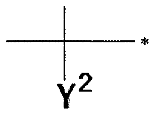
γΐ 및 γ2는 각각 독립적으로 수소, 치환 또는 비치환된 C1 내지 C30 알킬기 치환 또는 비치환된 C6 내지 C30 아릴기, 치환 또는 비치환된 C7 내지 C30 아릴알킬기, 치환 또는 비치환된 C1 내지 C30 헤테로알킬기, 치환 또는 비치환된 C2 내지 C30 헤테로고리기, 히드톡시기, 할로겐 원자 또는 이들의 조합이고,
*는 연결지점이다.
예를 들어, 상기 화학식 2에서 Υ1 및 Υ2 중 적어도 하나는 상기 그룹 2에 나열된 고리기에서 선택된 어느 하나이거나, 또는 상기 그룹 3에 나열된 헤테로 고리기에서 선택된 어느 하나일 수 있으나 이에 한정되는 것은 아니다.
상술한 중합체는 적어도 하나의 다환 고리기를 포함할 수 있다. 일 예로서, 상기 화학식 1에서 R1 및 R2 중 적어도 하나는 2 이상의 고리를 포함하는 다환 고리기일 수 있다. 다른 일 예로서, 상기 화학식 1에서 R3은 2이상의 고리를 포함하는 다환 고리기일 수 있다.
예를 들어, 상기 중합체는 약 500 내지 20,000의 중량평균분자량을 가질 수 있다. 상기 범위의 중량평균분자량을 가짐으로써 상기 중합체를 포함하는 유기막 조성물 (예컨대, 하드마스크 조성물)의 탄소 함량 및 용매에 대한 용해도를 조절하여 최적화할 수 있다.
상기 중합체를 유기막 재료로서 사용할 경우, 베이크 공정 중 핀-홀 및 보이드의 형성이나 두께 산포의 열화없이 균일한 박막을 형성할 수 있을 뿐만 아니라 하부 기판 (흑은 막)에 단차가존재하는 경우 혹은 패턴을 형성하는 경우 우수한 갭-필 및 평탄화 특성올 제공할 수 있다.
다른 구현예에 따르면, 상술한 중합체, 그리고 용매를 포함하는 유기막
조성물을 제공한다.
상기 용매는 상기 중합체에 대한 층분한 용해성 또는 분산성을 가지는 것이면 특별히 한정되지 않으나, 예컨대 프로필렌글리콜, 프로필렌글리콜
디아세테이트, 메특시 프로판디올, 디에틸렌글리콜, 디에틸렌글리콜 부틸에테르, 트리 (에틸렌글리콜)모노메틸에테르, 프로필렌글리콜 모노메틸에테르, 프로필렌글리콜 모노메틸에테르 아세테이트, 사이클로핵사논, 에틸락테이트, 감마 -부티로락톤 , Ν,Ν- 디메틸포름아미드, Ν,Ν-디메틸아세트아미드, 메틸피를리돈, 메틸피를리디논, 아세틸아세톤및 에틸 3-에톡시프로피오네이트에서 선택되는 적어도 하나를 포함할 수 있다ᅳ .
상기 중합체는 상기 유기막 조성물의 총 함량에 대하여 약 0.1 내지 50 중량0 /0로 포함될 수 있다. 상기 범위로 중합체가포함됨으로써 유기막의 두께, 표면 거칠기 및 평탄화 정도를 조절할 수 았다.
상기 유기막 조성물은 추가적으로 계면활성제, 가교제, 열산 발생제, 가소제 등의 첨가제를 더 포함할 수 있다.
상기 계면활성제는 예컨대 알킬벤젠설폰산 염, 알킬피리디늄 염,
폴리에틸렌글리콜, 게 4 암모늄 염 등을 사용할 수 있으나 이에 한정되는 것은 아니다.
상기 가교제는 예컨대 멜라민계, 치환요소계, 또는 이들 폴리머계 등을 들 수 있다. 바람직하게는, 적어도 2개의 가교 형성 치환기를 갖는 가교제로, 예를 들면, 메톡시메틸화 글리코루릴, 부톡시메틸화 글리코루릴, 메록시메틸화 멜라민, 부특시메틸화 멜라민, 메톡시메틸화 벤조구아나민, 부특시메틸화 벤조구아나민, 메특시메틸화요소, 부톡시메틸화요소, 메특시메틸화 티오요소, 또는 부톡시메틸화 티오요소 등의 화합물을 사용할 수 있다.
또한, 상기 가교제로는 내열성이 높은 가교제를 사용할 수 있다. 내열성이 높은 가교제로는 분자 내에 방향족 고리 (예를 들면 벤젠 고리, 나프탈렌 고리)을 가지는 가교 형성 치환기를 함유하는 화합물을 사용할 수 있다.
상기 열산발생제는 예컨대 Ρ-를루엔술폰산, 트리플루오로메탄술폰산, 피리디늄 ρ_를루엔술폰산, 살리실산, 술포살리실산, 구연산, 안식향산,
하이드록시안식향산, 나프탈렌카르본산 등의 산성 화합물 또는 /및 2,4,4,6- 테트라브로모시클로핵사디에논, 벤조인토실레이트, 2-니트로벤질토실레이트, 그 밖에
유기술폰산알킬에스테르 등을 사용할 수 있으나 이에 한정되는 것은 아니다.
상기 첨가제는 상기 유기막 조성물 100 중량부에 대하여 약 0.001 내지 40중량부로 포함될 수 있다. 상기 범위로 포함함으로써 유기막 조성물의 광학적 특성을 변경시키지 않으면서 용해도를 향상시킬 수 있다.
또 다른 구현예에 따르면, 상술한 유기막조성물을 사용하여 제조된
유기막을 제공한다. 상기 유기막은 상술한 유기막조성물을 예컨대 기판 위에 코팅한 후 열처리 과정을 통해 경화된 형태일 수 있으며, 예컨대 하드마스크 층, 평탄화 막, 회생막, 충진제, 등 전자 디바이스에 사용되는 유기 박막을 포함할 수 있다ᅳ
이하 상술한 유기막조성물올 사용하여 패턴을 형성하는 방법에 대하여 도
1를 참고하여 설명한다.
도 1은 일 구현예에 따른 패턴 형성 방법을 설명하는 흐름도이다.
일 구현예에 따른 패턴 형성 방법은 기판 위에 재료 층을 형성하는 단계 (S1), 상기 재료 층 위에 상술한 증합체 및 용매를 포함하는 유기막 조성물을 적용하는 단계 (S2), 상기 유기막 조성물을 열처리하여 하드마스크 층을 형성하는 단계 (S3), 상기 하드마스크 층 위에 실리콘 함유 박막층을 형성하는 단계 (S4), 상기 실리콘 함유 박막층 위에 포토레지스트 층을 형성하는 단계 (S5), 상기 포토레지스트 층을 노광 및 현상하여 포토레지스트 패턴을 형성하는 단계 (S6), 상기 포토레지스트 패턴을 이용하여 상기 실리콘 함유 박막층 및 상기 하드마스크 층을 선택적으로 제거하고 상기 재료 층의 일부를 노출하는 단계 (S7), 그리고 상기 재료 층의 노출된 부분을 식각하는 단계 (S8)를 포함한다.
상기 기판은 예컨대 실리콘웨이퍼, 유리 기판 또는 고분자 기판일 수 있다. 상기 재료 층은 최종적으로 패턴하고자 하는 재료이며, 예컨대 알루미늄, 구리 등과 같은 금속층, 실리콘과 같은 반도체 층 또는 산화규소, 질화규소 등과 같은 절연층일 수 있다. 상기 재료 층은 예컨대 화학기상증착 방법으로 형성될 수 있다.
상기 유기막 조성물은 전술한 바와 같으며, 용액 형태로 제조되어 스핀-온 코팅방법으로 도포될 수 있다. 이 때 상기 유기막 조성물의 도포 두께는 특별히 한정되지 않으나, 예컨대 약 50 내지 10,000 A 두께로 도포될 수 있다.
상기 유기막 조성물을 열처리하는 단계는 예컨대 약 100 내지 500 °C에서 약
10초 내지 1시간 동안수행할 수 있다.
상기 실리콘 함유 박막층은 예컨대 SiCN, SiOC, SiON, SiOCN, SiC, SiO및 /또는 SiN 등의 물질로 형성할 수 있다.
또한 상기 포토레지스트 층올 형성하는 단계 전에 상기 실리콘 함유 박막층 상부에 바닥 반사방지 층 (bottom anti-reflective coating, BARC)을 더 형성할 수도 있다. 상기 포토레지스트 층을 노광하는 단계는 예컨대 ArF, KrF 또는 EUV등을 사용하여 수행할 수 있다. 또한 노광 후 약 100 내지 500°C에서 열처리 공정을 수행할 수 있다.
상기 재료 층의 노출된 부분을 식각하는 단계는 식각 가스를 사용한 건식 식각으로 수행할 수 있으며, 식각 가스는 예컨대 CHF3, CF4, Cl2, BC13 및 이들의 흔합 가스를 사용할 수 있다.
상기 식각된 재료 층은 복수의 패턴으로 형성될 수 있으며, 상기 복수의 패턴은 금속 패턴, 반도체 패턴, 절연 패턴 등 다양할 수 있으며, 예컨대 반도체 집적 회로 디바이스 내의 다양한 패턴으로 적용될 수 있다.
【발명의 실시를 위한 형태】
이하 실시예를 통하여 상술한 본 발명의 구현예를 보다 상세하게 설명한다. 다만 하기의 실시예는 단지 설명의 목적을 위한 것이며 본 발명의 범위를 제한하는 것은 아니다.
. 줄
중합예 1
플라스크에 말로닐 클로라이드 (14.1g, 0.1mol)과 하이드록시파이렌 (43.7g, 0.2mol)를 1,2-다이클로로에탄 (319g)에 녹인 후 실온에서 교반하면서 알루미늄 클로라이드 (26,7g, 0.2mol)를 천천히 넣어준다음 1시간 추가로 교반시킨다.
반웅이 종결된 후, 반응물을 DIW(IL)에 천천히 적가한 다음 유기층을 빼준다. 유기층을 DIW(lOO mL)로 두 번 씻어준 후 감압 하에 유기용매를 제거하여 하기 화합물

<화합물 la>
얻어진 화합물 la (25.0g, 0.05mol)와 하이드라진 하이드로클로라이드 (6.9g, O.lmol)을 에탄올 150ml에 녹인 후 80°C에서 5시간 동안 교반하였다.
반응이 종결된 후, 차가운 DIW (500mL)에 천천히 적가한 다음 생성된 고체를 필터하고 용매를 제거하여 하기 화합물 lb를 얻었다.

<화합물 lb>
플라스크에 얻어진 화합물 lb (20.0g, 0.04mol)와
하이드록시파이렌카복스알데하이드 (9.9g, 0.04mol) 및 프로필렌글리콜
모노메틸에테르 아세테이트 120g을 첨가하여 용액을 준비하였다. 상기 용액에 다이에틸 설페이트 (0.31g)을 첨가한 후 100 °C에서 10 시간 동안 교반하였다.
중합이 완결되면, 메탄을에 침전시켜 모노머 및 저분자량체를 제거하여 하기 화학식 1-1로 표현되는 구조단위를 포함하는 중합체를 얻었다.
-1]

플라스크에 화합물 lb (20.0g, 0.04mol)와 트라이에틸아민 (40.5g, 0.4mol), 마그네슘클로라이드 (28.6g, 0.3mol), 파라품알데하이드 (14.4g)를 차례로 넣어준 다음 테트라하이드로퓨란 (414g)에 녹인 후 60 °C에서 24 시간 동안 교반하였다.
반웅이 종결된 후 상온으로 냉각한 다음 교반중인 DIW (500g)에 반웅물을 천천히 넣어준다. 생긴 고체들을 필터하고 DIW (300g)로 세번정도 씻어준다. 이후 고체를 diethyl ether (300g)에 풀어준 다음 다시 필터하고 감압 하에 잔류 용매를 제거하 하기 화합물 2a를 얻었다.

<화합물 2a>
얻어진 화합물 2a (l l.lg, 0.02mol)와 인돌 (2.3g, 0.02mol) 및 프로필렌글리콜 모노메틸에테르 아세테이트 68g을 첨가하여 용액을 준비하였다. 상기 용액에 다이에틸 설페이트 (0.15g)을 첨가한후 100 °C에서 10 시간 동안 교반하였다. 중합이 완결되면, 메탄올에 침전시켜 모노머 및 저분자량체를 제거하여 하기 화학식 1-2로 표현되는 구조단위를 포함하는 중합체를 얻었다ᅳ
-2]

-중합예 3
플라스크에 화합물 la (25. Og, 0.05mol)와 4-hydroxybenzamidine hydrochloride
(8.6g, 0.05mol),potassium carbonate (6.9g, 0.05mol)을 다이메틸폼아마이드 Oml에 녹인 후 80°C에서 5시간 동안 교반하였다.
반응이 종결된 후 상온으로 냉각한 다음 교반중인 DIW (800g)에 반웅물을 천천히 넣어준다. 생긴 고체들을 필터하고 DIW (300g)로 세번정도 씻어준다. 이후 고체를 에탄올 (300g)에 풀어준 다음 다시 필터하고 감압 하에 잔류 용매를 제거하 하기 화합물 3a를 얻었다.

<화합물 3a>
얻어진 화합물 3a (18.1g, 0.03mol)와 파이렌카복스알데하이드 (6.9g, ().03mol) 및 프로필렌글리콜 모노메틸에테르 아세테이트 100g을 첨가하여 용액을
준비하였다. 상기 용액에 다이에틸 설페이트 (0.23g)을 첨가한 후 100 °C에서 20 시간 동안 교반하였다. 중합이 완결되면, 메탄올에 침전시켜 모노머 및
저분자량체를 제거하여 하기 화학식 1-3으로 표현되는구조단위를 포함하는 중합체를 얻었다.
-3]

플라스크에 화합물 la (25.2g, 0.05mol)와 하이드록실아민 하이드로클로라이드 (6.9g, 0.10mol)을 넣고 에탄올 (150g)에 녹인 다음 80 °C에서 5시간 교반하였다. 반웅이 종결된 후 상온으로 냉각한 다음 교반중인 DIW (500g)에 반응물올 천천히 넣어준다. 생긴 고체들을 필터하고 diethyl ether (200g)에 풀어준 다음 다시 필터하고 하에 잔류 용매를 제거하여 하기 화합물 4a를 얻었다.
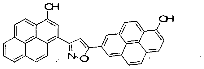
<화합물 4a>
얻어진 화합물 4a (15.0g, 0.03mol)와 파이렌카복스알데하이드 (6.9g, 0.03mol) 및 프로필렌글리콜 모노메틸에테르 아세테이트 100g을 첨가하여 용액을
준비하였다. 상기 용액에 다이에틸 설페이트 (0.23g)을 첨가한 후 100 °C에서 10 시간 동안 교반하였다. 중합이 완결되면, 메탄올에 침전시켜 모노머 및
저분자량체를 제거하여 하기 화학식 1-4로 표현되는 구조단위를 포함하는 중합체를 얻었다.
_4]

플라스크에 말로닐 클로라이드 (28.2g, 0.2mol)과 인들 (46.9g, 0.4mol)를 1,2- 다이클로로에탄 (400g)에 녹인 후 실온에서 교반하면서 알루미늄 클로라이드 (53.3g, 0.4mol)를 천천히 넣어준다음 1시간 추가로 교반시킨다.
반웅이 종결된 후, 반웅물을 DIW(IL)에 천천히 적가한 다음 유기층을 빼준다. 유기층을 DIW(lOO mL)로 두 번 씻어준 후 감압 하에 유기용매를 제거하여 하기 화합물 5a

<화합물 5a>
얻어진 화합물 5a (32.0g, 0.10mol)와 하이드라진 하이드로클로라이드 (13.7& 0.20mol)을 에탄올 250m 녹인 후 80°C에서 5시간 동안 교반하였다.
반응이 종결된 후, 차가운 DIW (500mL)에 천천히 적가한 다음 생성된 고체를 류 유기용매를 제거하여 하기 화합물 5b를 얻었다.

<화합물 5b>
플라스크에 얻어진 화합물 5b (14.9g, 0.05mol)와 파이렌카복스알데하이드 (11.5g, 0.05mol) 및 프로필렌글리콜 모노메틸에테르 아세테이트 120g을 첨가하여 용액을 준비하였다. 상기 용액에 다이에틸 설페이트 (0.39g)을 첨가한 후 100 °C에서 10 시간 동안 교반하였다. 중합이 완결되면, 메탄올에 침전시켜 모노머 및
저분자량체를 제거하여 하기 화학식 1-5로 표현되는 구조단위를 포함하는 중합체를 얻었다.
-5]
 비교중합예 1
플라스크에 1-나프를 28.83g(0.2 mol), 벤조퍼릴렌 41.4g (0.15 mol)및
파라포름알데히드 12.0g(0.34mol)을 투입한 이후에 프로필렌글리콜
모노메틸에테르아세테이트 (PGMEA) 162g을 넣어주었다. 다음으로 를루엔
술폰산모노하이드레이트 0.19g을 첨가한 후에 90 내지 100°C의 온도에서 5 내지
12시간 동안 교반하였다.
1시간 간격으로 상기 중합 반응물로부터 시료를 채취하여, 그 시료의 중량평균분자량을 측정하여, 중량평균분자량이 1,800 내지 2,500일 때 반웅을 완료하였다.
중합 반웅이 완료된 후, 반웅물을 상온으로 서서히 냉각한 후 상기 반웅물올 증류수 40g 및 메탄올 400g에 투입하여 강하게 교반한 후, 정치시켰다. 상등액을 제거하고 침전물을 프로필렌글리콜 모노메틸에테르아세테이트 (PGMEA) 80g에 녹인 후, 메탄올 320g를 이용하여 강하게 교반한 후, 정치시켰다 (1차). 이때 얻어지는 상등액을 다시 제거하고 침전물을 프로필렌글리콜
모노메틸에테르아세테이트 (PGMEA) 80g에 녹였다 (2차). 상기 1차 및 2차 공정을 1회 정제 공정이라 하고, 이 정제 공정을 총 3회 실시하였다. 정게가 끝난 중합체를 프로필렌글리콜 모노메틸에테르아세테이트 (PGMEA) 80g에 녹인 후, 감압 하에서 용액에 남아있는 메탄올 및 증류수를 제거하여 하기 화학식 A로 표현되는 구조단위를 포함하는 중합체를 얻었다.
[화학식 A]

플라스크에 9,9'-비스 (4-하이드록시페닐)플루오렌 5().0g(0.143 mol), 1,4- 비스 (메특시메틸)벤젠 23.7g(0.143 mol) 및 프로필렌글리콜 모노메틸에테르 아세테이트 50g을 첨가하여 용액을 준비하였다. 상기 용액에 다이에틸 설페이트 1.10g(7.13 mmol)을 첨가한 후 100 °C에서 24 시간 동안 교반하였다. 중합이 완결되면, 메탄올에 침전시켜 모노머 및 저분자량체를 제거하여 하기 화학식 B로 표현되는 구조단위를 포함하는 중합체를 얻었다.
[화학식 B]

플라스크에 파이를 5b (3.4g, 0.05mol)와 파이렌카복스알데하이드 (11.5g, 0.05mol) 및 프로필렌글리콜 모노메틸에테르 아세테이트 100g을 첨가하여 용액을 준비하였다. 상기 용액에 다이에틸 설페이트 (0.39g)올 첨가한 후 100 °C에서 5 시간 동안 교반하였다. 중합이 완결되면, 메탄올에 침전시켜 모노머 및 저분자량체를 제거하여 하기 화학식 C로 표현되는 구조단위를 포함하는 증합체를 얻었다.
C]

실시예 1
중합예 1에서 얻어진 중합체를 프로필렌글리콜 모노메틸에테르 아세테이트 (propylene glycol monomethyl ether acetate, PGMEA)와
사이클로핵사논 (cyclohexanone)(7:3 (v/v))의 흔합 용매에 녹인 후 여과하여 하드마스크 조성물을 제조하였다. 목적하고자 하는 두께에 따라상기 중합체의 중량은 상기 하드마스크 조성물의 총중량에 대하여 5.0 중량0 /0 내지 15.0 중량 %로 조절하였다.
실시예 2
중합예 1에서 얻은 중합체 대신 중합예 2에서 얻은 증합체를 사용한 것을
제외하고는 실시예 1과 동일한 방법으로 하드마스크 조성물을 제조하였다.
실시예 3
중합예 1에서 얻은 중합체 대신 중합예 3에서 얻은 중합체를 사용한 것을 제외하고는 실시예 1과 동일한 방법으로 하드마스크 조성물을 제조하였다.
실시예 4
중합예 1에서 얻은 중합체 대신 중합예 4에서 얻은 중합체를 사용한 것을 제외하고는 실시예 1과 동일한 방법으로 하드마스크 조성물을 제조하였다.
실시예 5
중합예 1에서 얻은 중합체 대신 중합예 5에서 얻은 중합체를 사용한 것을 제외하고는 실시예 1과 동일한 방법으로 하드마스크 조성물을 제조하였다.
비교예 1
중합예 1에서 얻은 중합체 대신 비교중합예 1에서 얻은 중합체를 사용한 것을 제외하고는 실시예 1과 동일한 방법으로 하드마스크 조성물을 제조하였다.
비교예 2
중합예 1에서 얻은 중합체 대신 비교중합예 2에서 얻은 중합체를사용한 것을 제외하고는 실시예 1과 동일한 방법으로 하드마스크 조성물올 제조하였다.
비교예 3
중합예 1에서 얻은 중합체 대신 비교증합예 3에서 얻은 중합체를 사용한 것을 제외하고는 실시예 1과 동일한 방법으로 하드마스크 조성물을 제조하였다. 평가 1: 내열성 평가
실시예 1 내지 실시예 5, 및 비교예 1에 따른 하드마스크 조성물 (중합체 함량: 10.0 중량0 /。)을 실리콘 웨이퍼 위에 스핀 코팅하고, 이어서 240 °C에서 2분 동안 열처리하여 박막을 형성한 후, K-MAC社의 박막두께측정기로 형성된 박막와두께를 측정하였다ᅳ
또한, 실시예 1 내지 실시예 5에 따른 하드마스크 조성물 (중합체 함량: 10.0 중량0 /。)을 실리콘 웨이퍼 위에 스핀 코팅하고, 이어서 400 °C에서 5분 동안
열처리하여 박막을 형성한 후 , Κ-MAC社의 박막두께측정기로 형성된 박막의 두께를 다시 축정하였다.
그 결과는 표 1과 같다.
【표 1]

박막은 비교예 1에 따른 하드마스크 조성물로부터 형성된 박막과 비교하여 섭씨 400도 열처리시 두께 감소율이 적은 것을 알 수 있다.
이로부터 실시예 1 내지 5에 따른 하드마스크 조성물은 비교예에 따른 하드마스크 조성물과 비교하여 내열성이 높은 것을 알 수 있다. 평가 2: 내식각성 평가
실리콘 웨이퍼 위에 실시예 1 내지 실시예 5, 그리고 비교예 1 내지 3에 따른 하드마스크 조성물 (증합체 함량 :10 중량0 /0)을 패턴이 형성된 실리콘 웨이퍼 위에 스핀-온 코팅 방법으로 코팅하였다. 이어서 ,400°C에서 2분간 열처리하여 박막을 형성한후 형성된 박막의 두께를 K-MAC社의 ST5000 박막 두께 측정기를 이용하여 측정하였다.
이어서, 상기 박막에 N2/02 흔합 가스 (50mT/300W/ 10Ο2/50Ν2)를 사용하여 각각 60초간 건식 식각을 실시한 후 박막의 두께를 다시 측정하였다. 건식 식각 전 후의 박막 두께와 식각 시간으로부터 하기 계산식 1에 의해 식각률 (bulk etch rate,
BER)을 계산하였다.
N2/02 흔합 가스대신 CFx 가스(10(^7 600\ /420^4/600^/ 1502)를 사용하여 120초 동안 건식 식각을 실시하여 마찬가지로 하기 계산식 1에 의해 식각률을 계산하였다.
[계산식 1]
Bulk etch rate (BER) = (초기 박막 두께 - 식각후 박막 두께) /식각'시간 (A/sec) 그 결과는 표 2와 같다.
【표 2】

표 1올 참고하면, 실시예 1 내지 실시예 5에 따른 하드마스크 조성물로부터 형성된 박막은 비교예 1 내지 3에 따른 하드마스크 조성물로부터 형성된 박막과 비교하여 N2/02 흔합 가스에 대한 식각율이 낮은 것을 알 수 있다. 또한, 실시예 1 내지 실시예 5에 따른 하드마스크 조성물로부터 형성된 박막은 비교예 1 내지 2에 따른 하드마스크 조성물로부터 형성된 박막과 비교하여 CFx 가스에 대한 식각율이 낮은 것을 알 수 있다.
이로부터 실시예 1 내지 실시예 5에 따른 하드마스크 조성물은 우수한 내식각성을 확보할 수 있음을 확인할 수 있다. 평가 3: 평탄화 특성 평가
실시예 1 내지 실시예 5, 및 비교예 1 내지 3에 따른 하드마스크 조성물 (중합체 함량: 5 중량 %)을 패턴화된 실리콘 웨이퍼 (트렌치 폭 ΙΟμηι, 트렌치 깊이 lOOnm)에 스핀-온 코팅하고 400°C에서 120초 동안 열처리하여 박막을 형성한 평탄화 특성을 관찰하였다.
평탄화 특성은 SEM으로 관찰한 패턴 단면의 이미지로부터 하드마스크 층의 두께를 측정하여 도 2에 나타낸 계산식 2로 수치화하였다. 도 2를 참고하면, 은 기판에서 패턴이 형성되지 않은 임의의 3개 지점에서 측정한 박막의 두께를 평균한 값을 의미하고, h2는 기판에서 패턴이 형성된 임의의 3개 지점에서 측정한 박막의 두께를 의미한다ᅳ 도 2를 참고하면, 평탄화 특성은 h, 및 h2의 차이가 크기 않을수록 우수한 것이므로, 평탄도 (planarization) 수치가 작을수록 평탄화 특성이
우수한 것이다.
한편, 갭-필 특성은 패턴의 단면을 전자 주사 현미경 (SEM)으로 관찰하여 보이드 (Void) 발생 유무를 판별하였다.
그 결과는 표 3과 같다.
【표 3】

표 3을 참고하면, 비교예 1 내지 3의 경우 hi과 h2의 차이가 커서 평탄화도가 매우 좋지 않으면서 패턴 내에 보이드 (Void) 역시 관찰되어 갭-필 성능도 떨어지는 것을 알 수 있다.
이에 반해, 실시예 1 내지 5에 따른 박막은 보이드가 관찰되지 않을 정도로 갭-필 성능이 좋을뿐더러 비교예 1 및 2와 비교하여 hi과 h2의 차이가 작은 것으로 미루어 평탄화 정도도 우수하다는 점을 확인할 수 있다. 이상에서 본 발명의 바람직한 실시예들에 대하여 상세하게 설명하였지만본 발명의 권리 범위는 이에 한정되는 것은 아니고 다음의 청구 범위에서 정의하고 있는 본 발명의 기본 개념을 이용한 당업자의 여러 변형 및 개량 형태 또한 본 발명의 권리 범위에 속하는 것이다.
Claims
[화학식 1]

상기 화학식 1에서,
A는 5각 또는 6각의 헤테로 방향족 고,리로서 동종 또는 이종의 헤테로 원자를 2개 이상 포함하고,
R1 및 R2는 각각 독립적으로 방향족 고리기, 헤테로 방향족 고리기, 또는 이들의 조합이고,
R3는 2가의 유기기이고,
*은 연결지점이다.
【청구항 2】
제 1항에서,
상기 화학식 1에서 A는 동종 또는 이종의 헤테로 원자를 2개 포함하고,
상기 2개의 헤테로 원자 중 적어도 하나는 질소 원자인
중합체.
【청구항 3】
저 12항에서,
상기 화학식 1에서 A는 2개의 질소 원자를 포함하는 6각의 헤테로 고리이거나, 1개의 질소 원자, 그리고 산소 원자 및 황 원자 중 1개를 포함하는 5각의 헤테로 고리인 중합체.
【청구항 4】
제 3항에서,
상기 화학식 1에서 A는 하기 그룹 1에 나열된 모이어티들 중 어느 하나인 중합체:
[그룹 i ]

상기 그룹 1에서,
X1 및 X2는 각각 질소 원자이고,
X3는 산소 원자, 황 원자 또는 NRa이고,
여기서 Ra는 수소, 치환 또는 비치환된 C1 내지 C30 알킬기, 치환또는 비치환된 C6 내지 C30 아릴기, 치환 또는 비치환된 C7 내지 C30 아릴알킬기, 치환 또는
비치환된 C1 내지 C30 헤테로알킬기, 치환 또는 비치환된 C2 내지 C30
헤테로고리기, 히드록시기, 할로겐 원자 또는 이들의 조합이고,
! 는 상기 Ra의 정의와 같다.
【청구항 5]
제 1항에서,
상기 화학식 1에서 R1 및 R2는 각각 독립적으로 하기 그룹 2 및 3 에 나열된 모이어티들 중에서 선택된 어느 하나인 중합체:
[그룹 2]


Z1 내지 Z3는 각각 독립적으로 산소 원자, 황 원자 또는 NRa이고,
여기서 Ra는 수소, 치환 또는 비치환된 C1 내지 C30 알킬기, 치환또는 비치환된 C6 내지 C30 아릴기, 치환또는 비치환된 C7 내지 C30 아릴알킬기, 치환또는
비치환된 C1 내지 C30 헤테로알킬기, 치환또는 비치환된 C2 내지 C30
헤테로고리기, 히드록시기, 할로겐 원자또는 이들의 조합이다.
【청구항 6]
제 1항에서,
상기 화학식 1에서 R3는 하기 화학식 2로 표현되는 중합체:
[화학식 2]

Υ1 및 Υ2는 각각 독립적으로 수소, 치환 또는 비치환된 C1 내지 C30 알킬기, 치환 또는 비치환된 C6 내지 C30 아릴기, 치환 또는 비치환된 C7 내지 C30 아릴알킬기 : 치환 또는 비치환된 C1 내지 C30 헤테로알킬기, 치환 또는 비치환된 C2 내지 C30 헤테로고리기, 히드록시기, 할로겐 원자 또는 이들의 조합이고,
*는 연결지점이다.
【청구항 7】
저 11항에서,
중량평균분자량이 500 내지 20,000인 중합체.
[청구항 8】
하기 화학식 1로 표현되는 구조 단위를 포함하는 증합체, 그리고
용매
를 포함하는 유기막 조성물:
[화학식 1]

Α는 5각 또는 6각의 헤테로 방향족 고리로서 동종 또는 이종의 헤테로 원자를 2개 이상 포함하고,
R1 및 R2는 각각 독립적으로 방향족 고리기, 헤테로 방향족 고리기, 또는 이들의 조합이고,
R3는 2가의 유기기이고,
*은 연결지점이다.
【청구항 9】
거 18항에서,
상기 화학식 1에서 A는 동종 또는 이종의 헤테로 원자를 2개 포함하고,
상기 2개의 해테로 원자 중 적어도 하나는 질소 원자인
유기막조성물.
【청구항 10]
제 9항에서,
상기 화학식 1에서 A는 2개의 질소 원자를 포함하는 6각의 헤테로 고리이거나, 1개의 질소 원자, 그리고 산소 원자 및 황 원자 중 1개를 포함하는 5각의 헤테로 고리인 유기막조성물.
【청구항 11 ]
제 10항에서,
상기 화학식 1에서 A는 하기 그룹 1에 나열된 모이어티들 중 어느 하나인 유기막 조성물:
[그룹 1]

상기 그룹 1에서,
X1 및 X2'는 각각 질소 원자이고,
X3는 산소 원자, 황 원자 또는 NRA이고,
여기서 RA는 수소, 치환또는 비치환된 C1 내지 C30 알킬기, 치환또는 비치환된 C6 내지 C30 아릴기, 치환또는 비치환된 C7 내지 C30 아릴알킬기, 치환 또는
비치환된 C1 내지 C30 헤테로알킬기, 치환또는 비치환된 C2 내지 C30
헤테로고리기, 히드록시기, 할로겐 원자또는 이들의 조합이고,
RC는 상기 RA의 정의와 같다.
【청구항 12]
제 8항에서,
상기 화학식 1에서 R1 및 R2는 각각 독립적으로 하기 그룹 2 및 3 에 나열된 모이어티들 중에서 선택된 어느 하나인 유기막 조성물:
[그룹 2]

[그룹 3]
 여기서 Ra는 수소, 치환 또는 비치환된 C1 내지 C30 알킬기, 치환 또는 비치환된 C6 내지 C30 아릴기, 치환 또는 비치환된 C7 내지 C30 아릴알킬기, 치환 또는
비치환된 C1 내지 C30 헤테로알킬기, 치환또는 비치환된 C2 내지 C30
헤테로고리기, 히드록시기, 할로겐 원자 또는 이들의 조합이다.
【청구항 13]
제 8항에서,
상기 화학식 1에서 R3는 하기 화학식 2로 표현되는 유기막 조성물:
[화학식 2]

Υ1 및 Υ2는 각각 독립적으로 수소, 치환 또는 비치환된 C1 내지 C30 알킬기, 치환 또는 비치환된 C6 내지 C30 아릴기, 치환또는 비치환된 C7 내지 C30 아릴알킬기: 치환또는 비치환된 C1 내지 C30 헤테로알킬기, 치환 또는 비치환된 C2 내지 C30 헤테로고리기, 히드록시기, 할로겐 원자 또는 이들의 조합이고,
*는 연결지점이다.
【청구항 14】
거 18항에서,
중량평균분자량이 500 내지 20,000인 유기막 조성물.
【청구항 15】
기판 위에 재료 층을 제공하는 단계,
상기 재료 층 위에 제 8항 내지 제 14항 중 어느 한 항에 따른 유기막 조성물을 적용하는 단계,
상기 유기막 조성물을 열처리하여 하드마스크 층을 형성하는 단계,
상기 하드마스크 층 위에 실리콘 함유 박막층을 형성하는 단계,
상기 실리콘 함유 박막층 위에 포토레지스트 층을 형성하는 단계,
상기 포토레지스트 층을 노광 및 현상하여 포토레지스트 패턴을 형성하는 단계 상기 포토레지스트 패턴을 이용하여 상기 실리콘 함유 박막층 및 상기 하드마스크
층을 선택적으로 제거하고 상기 재료 층의 일부를 노출하는 단계, 그리고 상기 재료 층의 노출된 부분을 식각하는 단계
를 포함하는 패턴 형성 방법.
【청구항 16]
제 15항에서,
상기 유기막 조성물을 적용하는 단계는 스핀-온 코팅 방법으로 수행하는 패턴 형성 방법.
【청구항 17】
제 15항에서,
상기 포토레지스트 층을 형성하는 단계 전에 바닥 반사 방지 층 (BARC)을 형성하는 단계를 더 포함하는 패턴 형성 방법.
Applications Claiming Priority (2)
| Application Number | Priority Date | Filing Date | Title |
|---|---|---|---|
| KR10-2016-0141244 | 2016-10-27 | ||
| KR1020160141244A KR101994367B1 (ko) | 2016-10-27 | 2016-10-27 | 중합체, 하드마스크 조성물 및 패턴형성방법 |
Publications (1)
| Publication Number | Publication Date |
|---|---|
| WO2018079936A1 true WO2018079936A1 (ko) | 2018-05-03 |
Family
ID=62025093
Family Applications (1)
| Application Number | Title | Priority Date | Filing Date |
|---|---|---|---|
| PCT/KR2016/015409 Ceased WO2018079936A1 (ko) | 2016-10-27 | 2016-12-28 | 중합체, 유기막 조성물 및 패턴형성방법 |
Country Status (3)
| Country | Link |
|---|---|
| KR (1) | KR101994367B1 (ko) |
| TW (1) | TWI641913B (ko) |
| WO (1) | WO2018079936A1 (ko) |
Families Citing this family (7)
| Publication number | Priority date | Publication date | Assignee | Title |
|---|---|---|---|---|
| KR102171075B1 (ko) * | 2018-07-12 | 2020-10-28 | 삼성에스디아이 주식회사 | 중합체, 하드마스크 조성물 및 패턴 형성 방법 |
| KR102244470B1 (ko) * | 2018-07-18 | 2021-04-23 | 삼성에스디아이 주식회사 | 중합체, 유기막 조성물 및 패턴 형성 방법 |
| KR102303554B1 (ko) * | 2018-12-26 | 2021-09-16 | 삼성에스디아이 주식회사 | 중합체, 하드마스크 조성물 및 패턴 형성 방법 |
| KR102843509B1 (ko) * | 2020-02-21 | 2025-08-07 | 동우 화인켐 주식회사 | 하드마스크용 조성물 |
| KR102767266B1 (ko) * | 2020-12-23 | 2025-02-11 | 삼성에스디아이 주식회사 | 하드마스크 조성물, 하드마스크 층 및 패턴 형성 방법 |
| KR102745437B1 (ko) * | 2021-09-07 | 2024-12-19 | 삼성에스디아이 주식회사 | 하드마스크 조성물, 하드마스크 층 및 패턴 형성 방법 |
| KR102936650B1 (ko) | 2023-05-31 | 2026-03-06 | 삼성에스디아이 주식회사 | 하드마스크 조성물, 하드마스크 층 및 패턴 형성 방법 |
Citations (5)
| Publication number | Priority date | Publication date | Assignee | Title |
|---|---|---|---|---|
| WO1996020253A1 (en) * | 1994-12-28 | 1996-07-04 | Cambridge Display Technology Ltd. | Polymers for use in optical devices |
| JP2006259249A (ja) * | 2005-03-17 | 2006-09-28 | Shin Etsu Chem Co Ltd | フォトレジスト下層膜形成材料及びパターン形成方法 |
| KR100819162B1 (ko) * | 2007-04-24 | 2008-04-03 | 제일모직주식회사 | 반사방지성을 갖는 하드마스크 조성물 및 이를 이용한재료의 패턴화 방법 |
| KR20140069163A (ko) * | 2011-09-29 | 2014-06-09 | 닛산 가가쿠 고교 가부시키 가이샤 | 디아릴아민 노볼락 수지 |
| KR20140144207A (ko) * | 2012-03-27 | 2014-12-18 | 닛산 가가쿠 고교 가부시키 가이샤 | 페닐인돌 함유 노볼락 수지를 포함하는 레지스트 하층막 형성 조성물 |
Family Cites Families (2)
| Publication number | Priority date | Publication date | Assignee | Title |
|---|---|---|---|---|
| DE102006036019A1 (de) * | 2006-08-02 | 2008-02-07 | Pemeas Gmbh | Membran-Elektroden-Einheit und Brennstoffzellen mit erhöhter Leistung |
| KR101667788B1 (ko) * | 2013-12-31 | 2016-10-19 | 제일모직 주식회사 | 하드마스크 조성물 및 이를 사용한 패턴 형성 방법 |
-
2016
- 2016-10-27 KR KR1020160141244A patent/KR101994367B1/ko active Active
- 2016-12-28 WO PCT/KR2016/015409 patent/WO2018079936A1/ko not_active Ceased
-
2017
- 2017-04-17 TW TW106112730A patent/TWI641913B/zh active
Patent Citations (5)
| Publication number | Priority date | Publication date | Assignee | Title |
|---|---|---|---|---|
| WO1996020253A1 (en) * | 1994-12-28 | 1996-07-04 | Cambridge Display Technology Ltd. | Polymers for use in optical devices |
| JP2006259249A (ja) * | 2005-03-17 | 2006-09-28 | Shin Etsu Chem Co Ltd | フォトレジスト下層膜形成材料及びパターン形成方法 |
| KR100819162B1 (ko) * | 2007-04-24 | 2008-04-03 | 제일모직주식회사 | 반사방지성을 갖는 하드마스크 조성물 및 이를 이용한재료의 패턴화 방법 |
| KR20140069163A (ko) * | 2011-09-29 | 2014-06-09 | 닛산 가가쿠 고교 가부시키 가이샤 | 디아릴아민 노볼락 수지 |
| KR20140144207A (ko) * | 2012-03-27 | 2014-12-18 | 닛산 가가쿠 고교 가부시키 가이샤 | 페닐인돌 함유 노볼락 수지를 포함하는 레지스트 하층막 형성 조성물 |
Also Published As
| Publication number | Publication date |
|---|---|
| TW201816517A (zh) | 2018-05-01 |
| TWI641913B (zh) | 2018-11-21 |
| KR101994367B1 (ko) | 2019-06-28 |
| KR20180046236A (ko) | 2018-05-08 |
Similar Documents
| Publication | Publication Date | Title |
|---|---|---|
| KR101994367B1 (ko) | 중합체, 하드마스크 조성물 및 패턴형성방법 | |
| KR101829750B1 (ko) | 중합체, 유기막 조성물, 및 패턴형성방법 | |
| US9158201B2 (en) | Monomer for hardmask composition and hardmask composition including the monomer and method of forming patterns using the hardmask composition | |
| TWI644999B (zh) | 聚合物、有機層組成物與形成圖案之方法 | |
| WO2017126780A1 (ko) | 유기막 조성물, 및 패턴형성방법 | |
| WO2018021619A1 (ko) | 유기막 조성물 및 패턴형성방법 | |
| TWI535697B (zh) | 硬罩幕組成物與其使用的單體及其圖案形成方法 | |
| TW201932979A (zh) | 硬罩幕組成物與形成圖案的方法 | |
| KR102134268B1 (ko) | 모노머, 중합체, 유기막 조성물 및 패턴 형성 방법 | |
| KR101976016B1 (ko) | 중합체, 유기막 조성물 및 패턴형성방법 | |
| KR101991698B1 (ko) | 화합물, 유기막 조성물, 및 패턴형성방법 | |
| CN106084159B (zh) | 聚合物、有机层组合物以及形成图案的方法 | |
| CN110734528A (zh) | 聚合物、有机层组合物以及形成图案的方法 | |
| KR102036681B1 (ko) | 화합물, 유기막 조성물, 및 패턴형성방법 | |
| KR102246692B1 (ko) | 화합물, 유기막 조성물, 유기막 및 패턴 형성 방법 | |
| KR102134266B1 (ko) | 모노머, 중합체, 유기막 조성물 및 패턴 형성 방법 | |
| KR102129511B1 (ko) | 화합물, 유기막 조성물, 및 패턴 형성 방법 | |
| US20160237306A1 (en) | Monomer, organic layer composition, organic layer, and method of forming patterns | |
| KR102018237B1 (ko) | 중합체, 유기막 조성물 및 패턴형성방법 | |
| TWI880684B (zh) | 硬遮罩組合物、硬遮罩層以及形成圖案的方法 | |
| KR102284581B1 (ko) | 화합물, 유기막 조성물 및 패턴 형성 방법 | |
| KR101994366B1 (ko) | 중합체, 유기막 조성물 및 패턴형성방법 | |
| KR102151674B1 (ko) | 중합체, 유기막 조성물 및 패턴 형성 방법 | |
| TW201823295A (zh) | 有機層組成物、有機層以及形成圖案的方法 | |
| KR20180138405A (ko) | 유기막 조성물, 중합체 및 패턴 형성 방법 |
Legal Events
| Date | Code | Title | Description |
|---|---|---|---|
| 121 | Ep: the epo has been informed by wipo that ep was designated in this application |
Ref document number: 16919686 Country of ref document: EP Kind code of ref document: A1 |
|
| NENP | Non-entry into the national phase |
Ref country code: DE |
|
| 122 | Ep: pct application non-entry in european phase |
Ref document number: 16919686 Country of ref document: EP Kind code of ref document: A1 |