WO2018074135A1 - 蓄電装置及び蓄電装置の製造方法 - Google Patents
蓄電装置及び蓄電装置の製造方法 Download PDFInfo
- Publication number
- WO2018074135A1 WO2018074135A1 PCT/JP2017/034103 JP2017034103W WO2018074135A1 WO 2018074135 A1 WO2018074135 A1 WO 2018074135A1 JP 2017034103 W JP2017034103 W JP 2017034103W WO 2018074135 A1 WO2018074135 A1 WO 2018074135A1
- Authority
- WO
- WIPO (PCT)
- Prior art keywords
- resin member
- bipolar electrodes
- storage device
- power storage
- current collector
- Prior art date
- Legal status (The legal status is an assumption and is not a legal conclusion. Google has not performed a legal analysis and makes no representation as to the accuracy of the status listed.)
- Ceased
Links
Images


Classifications
-
- H—ELECTRICITY
- H01—ELECTRIC ELEMENTS
- H01M—PROCESSES OR MEANS, e.g. BATTERIES, FOR THE DIRECT CONVERSION OF CHEMICAL ENERGY INTO ELECTRICAL ENERGY
- H01M4/00—Electrodes
- H01M4/02—Electrodes composed of, or comprising, active material
- H01M4/64—Carriers or collectors
- H01M4/70—Carriers or collectors characterised by shape or form
-
- H—ELECTRICITY
- H01—ELECTRIC ELEMENTS
- H01G—CAPACITORS; CAPACITORS, RECTIFIERS, DETECTORS, SWITCHING DEVICES, LIGHT-SENSITIVE OR TEMPERATURE-SENSITIVE DEVICES OF THE ELECTROLYTIC TYPE
- H01G11/00—Hybrid capacitors, i.e. capacitors having different positive and negative electrodes; Electric double-layer [EDL] capacitors; Processes for the manufacture thereof or of parts thereof
- H01G11/10—Multiple hybrid or EDL capacitors, e.g. arrays or modules
- H01G11/12—Stacked hybrid or EDL capacitors
-
- H—ELECTRICITY
- H01—ELECTRIC ELEMENTS
- H01G—CAPACITORS; CAPACITORS, RECTIFIERS, DETECTORS, SWITCHING DEVICES, LIGHT-SENSITIVE OR TEMPERATURE-SENSITIVE DEVICES OF THE ELECTROLYTIC TYPE
- H01G11/00—Hybrid capacitors, i.e. capacitors having different positive and negative electrodes; Electric double-layer [EDL] capacitors; Processes for the manufacture thereof or of parts thereof
- H01G11/74—Terminals, e.g. extensions of current collectors
- H01G11/76—Terminals, e.g. extensions of current collectors specially adapted for integration in multiple or stacked hybrid or EDL capacitors
-
- H—ELECTRICITY
- H01—ELECTRIC ELEMENTS
- H01G—CAPACITORS; CAPACITORS, RECTIFIERS, DETECTORS, SWITCHING DEVICES, LIGHT-SENSITIVE OR TEMPERATURE-SENSITIVE DEVICES OF THE ELECTROLYTIC TYPE
- H01G11/00—Hybrid capacitors, i.e. capacitors having different positive and negative electrodes; Electric double-layer [EDL] capacitors; Processes for the manufacture thereof or of parts thereof
- H01G11/78—Cases; Housings; Encapsulations; Mountings
- H01G11/80—Gaskets; Sealings
-
- H—ELECTRICITY
- H01—ELECTRIC ELEMENTS
- H01G—CAPACITORS; CAPACITORS, RECTIFIERS, DETECTORS, SWITCHING DEVICES, LIGHT-SENSITIVE OR TEMPERATURE-SENSITIVE DEVICES OF THE ELECTROLYTIC TYPE
- H01G11/00—Hybrid capacitors, i.e. capacitors having different positive and negative electrodes; Electric double-layer [EDL] capacitors; Processes for the manufacture thereof or of parts thereof
- H01G11/78—Cases; Housings; Encapsulations; Mountings
- H01G11/82—Fixing or assembling a capacitive element in a housing, e.g. mounting electrodes, current collectors or terminals in containers or encapsulations
-
- H—ELECTRICITY
- H01—ELECTRIC ELEMENTS
- H01G—CAPACITORS; CAPACITORS, RECTIFIERS, DETECTORS, SWITCHING DEVICES, LIGHT-SENSITIVE OR TEMPERATURE-SENSITIVE DEVICES OF THE ELECTROLYTIC TYPE
- H01G11/00—Hybrid capacitors, i.e. capacitors having different positive and negative electrodes; Electric double-layer [EDL] capacitors; Processes for the manufacture thereof or of parts thereof
- H01G11/84—Processes for the manufacture of hybrid or EDL capacitors, or components thereof
- H01G11/86—Processes for the manufacture of hybrid or EDL capacitors, or components thereof specially adapted for electrodes
-
- H—ELECTRICITY
- H01—ELECTRIC ELEMENTS
- H01M—PROCESSES OR MEANS, e.g. BATTERIES, FOR THE DIRECT CONVERSION OF CHEMICAL ENERGY INTO ELECTRICAL ENERGY
- H01M10/00—Secondary cells; Manufacture thereof
- H01M10/04—Construction or manufacture in general
-
- H—ELECTRICITY
- H01—ELECTRIC ELEMENTS
- H01M—PROCESSES OR MEANS, e.g. BATTERIES, FOR THE DIRECT CONVERSION OF CHEMICAL ENERGY INTO ELECTRICAL ENERGY
- H01M10/00—Secondary cells; Manufacture thereof
- H01M10/04—Construction or manufacture in general
- H01M10/0413—Large-sized flat cells or batteries for motive or stationary systems with plate-like electrodes
- H01M10/0418—Large-sized flat cells or batteries for motive or stationary systems with plate-like electrodes with bipolar electrodes
-
- H—ELECTRICITY
- H01—ELECTRIC ELEMENTS
- H01M—PROCESSES OR MEANS, e.g. BATTERIES, FOR THE DIRECT CONVERSION OF CHEMICAL ENERGY INTO ELECTRICAL ENERGY
- H01M10/00—Secondary cells; Manufacture thereof
- H01M10/04—Construction or manufacture in general
- H01M10/0486—Frames for plates or membranes
-
- H—ELECTRICITY
- H01—ELECTRIC ELEMENTS
- H01M—PROCESSES OR MEANS, e.g. BATTERIES, FOR THE DIRECT CONVERSION OF CHEMICAL ENERGY INTO ELECTRICAL ENERGY
- H01M10/00—Secondary cells; Manufacture thereof
- H01M10/05—Accumulators with non-aqueous electrolyte
- H01M10/052—Li-accumulators
- H01M10/0525—Rocking-chair batteries, i.e. batteries with lithium insertion or intercalation in both electrodes; Lithium-ion batteries
-
- H—ELECTRICITY
- H01—ELECTRIC ELEMENTS
- H01M—PROCESSES OR MEANS, e.g. BATTERIES, FOR THE DIRECT CONVERSION OF CHEMICAL ENERGY INTO ELECTRICAL ENERGY
- H01M10/00—Secondary cells; Manufacture thereof
- H01M10/05—Accumulators with non-aqueous electrolyte
- H01M10/058—Construction or manufacture
- H01M10/0585—Construction or manufacture of accumulators having only flat construction elements, i.e. flat positive electrodes, flat negative electrodes and flat separators
-
- H—ELECTRICITY
- H01—ELECTRIC ELEMENTS
- H01M—PROCESSES OR MEANS, e.g. BATTERIES, FOR THE DIRECT CONVERSION OF CHEMICAL ENERGY INTO ELECTRICAL ENERGY
- H01M10/00—Secondary cells; Manufacture thereof
- H01M10/24—Alkaline accumulators
- H01M10/30—Nickel accumulators
-
- H—ELECTRICITY
- H01—ELECTRIC ELEMENTS
- H01M—PROCESSES OR MEANS, e.g. BATTERIES, FOR THE DIRECT CONVERSION OF CHEMICAL ENERGY INTO ELECTRICAL ENERGY
- H01M4/00—Electrodes
- H01M4/02—Electrodes composed of, or comprising, active material
- H01M4/64—Carriers or collectors
-
- H—ELECTRICITY
- H01—ELECTRIC ELEMENTS
- H01M—PROCESSES OR MEANS, e.g. BATTERIES, FOR THE DIRECT CONVERSION OF CHEMICAL ENERGY INTO ELECTRICAL ENERGY
- H01M50/00—Constructional details or processes of manufacture of the non-active parts of electrochemical cells other than fuel cells, e.g. hybrid cells
- H01M50/10—Primary casings; Jackets or wrappings
- H01M50/102—Primary casings; Jackets or wrappings characterised by their shape or physical structure
- H01M50/103—Primary casings; Jackets or wrappings characterised by their shape or physical structure prismatic or rectangular
-
- H—ELECTRICITY
- H01—ELECTRIC ELEMENTS
- H01M—PROCESSES OR MEANS, e.g. BATTERIES, FOR THE DIRECT CONVERSION OF CHEMICAL ENERGY INTO ELECTRICAL ENERGY
- H01M50/00—Constructional details or processes of manufacture of the non-active parts of electrochemical cells other than fuel cells, e.g. hybrid cells
- H01M50/50—Current conducting connections for cells or batteries
- H01M50/572—Means for preventing undesired use or discharge
- H01M50/584—Means for preventing undesired use or discharge for preventing incorrect connections inside or outside the batteries
- H01M50/586—Means for preventing undesired use or discharge for preventing incorrect connections inside or outside the batteries inside the batteries, e.g. incorrect connections of electrodes
-
- H—ELECTRICITY
- H01—ELECTRIC ELEMENTS
- H01M—PROCESSES OR MEANS, e.g. BATTERIES, FOR THE DIRECT CONVERSION OF CHEMICAL ENERGY INTO ELECTRICAL ENERGY
- H01M50/00—Constructional details or processes of manufacture of the non-active parts of electrochemical cells other than fuel cells, e.g. hybrid cells
- H01M50/50—Current conducting connections for cells or batteries
- H01M50/572—Means for preventing undesired use or discharge
- H01M50/584—Means for preventing undesired use or discharge for preventing incorrect connections inside or outside the batteries
- H01M50/59—Means for preventing undesired use or discharge for preventing incorrect connections inside or outside the batteries characterised by the protection means
- H01M50/593—Spacers; Insulating plates
-
- H—ELECTRICITY
- H01—ELECTRIC ELEMENTS
- H01M—PROCESSES OR MEANS, e.g. BATTERIES, FOR THE DIRECT CONVERSION OF CHEMICAL ENERGY INTO ELECTRICAL ENERGY
- H01M4/00—Electrodes
- H01M4/02—Electrodes composed of, or comprising, active material
- H01M2004/026—Electrodes composed of, or comprising, active material characterised by the polarity
- H01M2004/029—Bipolar electrodes
-
- Y—GENERAL TAGGING OF NEW TECHNOLOGICAL DEVELOPMENTS; GENERAL TAGGING OF CROSS-SECTIONAL TECHNOLOGIES SPANNING OVER SEVERAL SECTIONS OF THE IPC; TECHNICAL SUBJECTS COVERED BY FORMER USPC CROSS-REFERENCE ART COLLECTIONS [XRACs] AND DIGESTS
- Y02—TECHNOLOGIES OR APPLICATIONS FOR MITIGATION OR ADAPTATION AGAINST CLIMATE CHANGE
- Y02E—REDUCTION OF GREENHOUSE GAS [GHG] EMISSIONS, RELATED TO ENERGY GENERATION, TRANSMISSION OR DISTRIBUTION
- Y02E60/00—Enabling technologies; Technologies with a potential or indirect contribution to GHG emissions mitigation
- Y02E60/10—Energy storage using batteries
-
- Y—GENERAL TAGGING OF NEW TECHNOLOGICAL DEVELOPMENTS; GENERAL TAGGING OF CROSS-SECTIONAL TECHNOLOGIES SPANNING OVER SEVERAL SECTIONS OF THE IPC; TECHNICAL SUBJECTS COVERED BY FORMER USPC CROSS-REFERENCE ART COLLECTIONS [XRACs] AND DIGESTS
- Y02—TECHNOLOGIES OR APPLICATIONS FOR MITIGATION OR ADAPTATION AGAINST CLIMATE CHANGE
- Y02P—CLIMATE CHANGE MITIGATION TECHNOLOGIES IN THE PRODUCTION OR PROCESSING OF GOODS
- Y02P70/00—Climate change mitigation technologies in the production process for final industrial or consumer products
- Y02P70/50—Manufacturing or production processes characterised by the final manufactured product
Definitions
- One aspect of the present invention relates to a power storage device and a method for manufacturing the power storage device.
- a bipolar battery having a bipolar electrode in which a positive electrode is formed on one surface of a current collector and a negative electrode is formed on the other surface is known.
- a bipolar battery a plurality of bipolar electrodes are stacked in series across an electrolyte layer.
- the polypropylene layer covers the periphery of a bipolar plate (current collector) using a metal such as nickel.
- a polypropylene layer and a polypropylene cell casing for supporting a plurality of current collectors are fixed together by integral molding.
- a bipolar plate covered with the polypropylene layer is placed in a mold, and the polypropylene is injected into the mold to perform injection molding (insert molding method).
- An object of one aspect of the present invention is to provide a power storage device and a method for manufacturing the power storage device in which positional deviation between adjacent bipolar electrodes is suppressed.
- the power storage device includes a plurality of stacked bipolar electrodes, and each of the plurality of bipolar electrodes has a first surface and a second surface opposite to the first surface.
- a second resin member that supports the outer peripheral portion of the current collector via a resin member, and the first resin members of the bipolar electrodes adjacent to each other in the stacking direction of the plurality of bipolar electrodes are Are connected by a welded part.
- the first resin members of the bipolar electrodes adjacent in the stacking direction of the plurality of bipolar electrodes are connected to each other by the welded portion. Therefore, even when pressure is applied to the bipolar electrode when forming the second resin member, it is possible to suppress positional deviation between adjacent bipolar electrodes.
- the second resin member may cover the outside of the first resin member.
- the weld portion may be provided on an outer end surface of the first resin member, and may extend from one bipolar electrode to the other bipolar electrode in the stacking direction of the plurality of bipolar electrodes.
- the welded portion may have a cylindrical shape and may be disposed so as to surround the entire circumference of the outer peripheral portion of the current collector.
- the welding portion may be arranged on each side of the current collector having a rectangular shape when viewed from the stacking direction of the plurality of bipolar electrodes.
- the effect of suppressing the positional deviation between the adjacent bipolar electrodes is greater than in the case where the welded portion is disposed at each vertex of the current collector.
- a method for manufacturing a power storage device includes a plurality of stacked bipolar electrodes, and each of the plurality of bipolar electrodes has a first surface and a second surface opposite to the first surface.
- a method of manufacturing a power storage device comprising: a current collector having a surface; a positive electrode layer provided on the first surface; and a negative electrode layer provided on the second surface, A step of providing a first resin member on at least one of the first surface and the second surface in at least a part of an outer peripheral portion of the current collector of each of a plurality of bipolar electrodes; A step of laminating the bipolar electrodes, a step of welding the first resin members of each of the bipolar electrodes adjacent in the laminating direction of the plurality of bipolar electrodes, and an outer side of the first resin members welded to each other Covering the first And forming a second resin member for supporting the outer peripheral portion of the current collector via the resin member by injection molding, a.
- a power storage device and a method for manufacturing the power storage device in which positional deviation between adjacent bipolar electrodes is suppressed can be provided.
- FIG. 4 is a cross-sectional view of the power storage device along line IV-IV in FIG. 1.
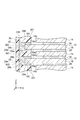
- FIG. 1 is a cross-sectional view schematically showing a power storage device according to an embodiment.
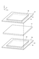
- FIG. 2 is an exploded perspective view schematically showing a part of the power storage device according to the embodiment.
- the power storage device 10 shown in FIG. 1 may be a secondary battery such as a nickel hydride secondary battery or a lithium ion secondary battery, or may be an electric double layer capacitor.
- the power storage device 10 can be mounted on a vehicle such as a forklift, a hybrid vehicle, or an electric vehicle.
- the power storage device 10 includes a plurality of bipolar electrodes 12.
- the plurality of bipolar electrodes 12 are stacked in series via the separator 14.
- Each of the bipolar electrodes 12 includes a current collector 16 having a first surface 16a and a second surface 16b opposite to the first surface 16a, and a positive electrode layer 18 provided on the first surface 16a. And a negative electrode layer 20 provided on the second surface 16b.
- the positive electrode layer 18 and the negative electrode layer 20 extend along a plane (for example, an XY plane) that intersects the stacking direction of the plurality of bipolar electrodes 12 (hereinafter also referred to as the Z-axis direction).
- the separator 14 may be a sheet shape or a bag shape.
- the separator 14 is a porous film or a nonwoven fabric, for example.
- the separator 14 can permeate the electrolytic solution.
- Examples of the material of the separator 14 include polyolefins such as polyethylene and polypropylene, polyamides such as polyimide and aramid fibers, and the like.
- a separator 14 reinforced with a vinylidene fluoride resin compound may be used.
- As the electrolytic solution for example, an alkaline solution such as an aqueous potassium hydroxide solution can be used.
- the current collector 16 may be a metal foil such as a nickel foil, or may be a conductive resin member such as a conductive resin film.
- the thickness of the current collector 16 is, for example, 0.1 to 1000 ⁇ m.
- the positive electrode layer 18 includes a positive electrode active material.
- the positive electrode active material is, for example, nickel hydroxide (Ni (OH) 2 ) particles.
- the positive electrode active material is, for example, a composite oxide, metallic lithium, sulfur, or the like.
- the negative electrode layer 20 includes a negative electrode active material.
- the negative electrode active material is, for example, particles of a hydrogen storage alloy.
- the negative electrode active material is, for example, carbon such as graphite, highly oriented graphite, mesocarbon microbeads, hard carbon, and soft carbon, alkali metals such as lithium and sodium, metal compounds, Examples thereof include metal oxides such as SiO x (0.5 ⁇ x ⁇ 1.5), boron-added carbon and the like.
- the plurality of bipolar electrodes 12 and the plurality of separators 14 may be sandwiched between the electrode 112 and the electrode 212.
- the electrode 112 and the electrode 212 are electrodes located on the outermost side in the Z-axis direction.
- the electrode 112 includes a current collector 116 and a positive electrode layer 18 provided on the surface of the current collector 116 on the separator 14 side.
- the electrode 212 includes a current collector 116 and a negative electrode layer 20 provided on the surface of the current collector 116 on the separator 14 side.
- the current collector 116 has the same configuration as the current collector 16 except that it is thicker than the current collector 16 in the Z-axis direction.
- the power storage device 10 includes a resin member 28 (first resin member) and an insulating case 30 (second resin member).
- the resin member 28 is provided on the outer peripheral portion 161 (see FIG. 3 described later) of the current collector 16. Adjacent resin members 28 in the Z-axis direction are connected by a welded portion 128.
- the insulating case 30 is a resin case that supports the plurality of bipolar electrodes 12 via the resin member 28.
- the material of the insulating case 30 may be the same as or different from the material of the resin member 28.
- the insulating case 30 is, for example, a case made of polyparaphenylene benzobisoxazole (Zylon (registered trademark)).
- the insulating case 30 may support the electrode 112 and the electrode 212.
- the insulating case 30 may be a cylindrical member that can accommodate the plurality of bipolar electrodes 12 and the plurality of separators 14. An electrolytic solution is accommodated in the insulating case 30. Details of the resin member 28, the insulating case 30, and the welded portion 128 will be described later with reference to FIGS.
- the power storage device 10 may include a positive electrode plate 40 and a negative electrode plate 50.
- the positive electrode plate 40 and the negative electrode plate 50 sandwich the plurality of bipolar electrodes 12 and the plurality of separators 14 in the Z-axis direction.
- the positive electrode plate 40 and the negative electrode plate 50 may sandwich the electrode 112, the electrode 212, and the insulating case 30.
- the electrode 112 is disposed between the positive electrode plate 40 and the separator 14.
- the electrode 212 is disposed between the negative electrode plate 50 and the separator 14.
- a positive electrode terminal 42 is connected to the positive electrode plate 40.
- a negative electrode terminal 52 is connected to the negative electrode plate 50.
- the positive and negative terminals 42 and 52 can charge and discharge the power storage device 10.
- the positive electrode plate 40 and the negative electrode plate 50 are provided with through holes for passing through the bolts B extending in the Z-axis direction.
- the through hole is disposed outside the insulating case 30 when viewed from the Z-axis direction.
- the bolt B can be inserted from the positive electrode plate 40 toward the negative electrode plate 50 while being insulated from the positive electrode plate 40 and the negative electrode plate 50.
- a nut N is screwed to the tip of the bolt B.
- the positive electrode plate 40 and the negative electrode plate 50 can restrain the plurality of bipolar electrodes 12, the plurality of separators 14, the electrodes 112, the electrodes 212, and the insulating case 30.
- the inside of the insulating case 30 can be sealed.
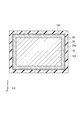
- FIG. 3 is an enlarged cross-sectional view of the resin member 28, the insulating case 30, and the welded portion 128.
- the resin member 28 is provided on at least a part of the outer peripheral portion 161 of the current collector 16.
- the resin member 28 may be provided in an annular shape over the entire outer peripheral portion 161.
- the resin member 28 is provided on at least one of the first surface 16 a and the second surface 16 b of the current collector 16. In the example shown in FIG. 3, the resin member 28 is provided on both the first surface 16 a and the second surface 16 b of the current collector 16.
- the resin member 28 has a contact surface 28 a that contacts the first surface 16 a of the current collector 16 and a contact surface 28 b that contacts the second surface 16 b of the current collector 16.
- the resin member 28 may also be provided on the end surface 16c of the current collector 16, and in this case, the resin member 28 also has a contact surface 28c that contacts the end surface 16c of the current collector 16.
- the end surface 16c is a surface that connects the first surface 16a and the second surface 16b.
- the contact surface 28c is a surface that connects the contact surface 28a and the contact surface 28b.
- the resin member 28 has a U-shaped cross section as viewed from the direction orthogonal to the outer peripheral direction of the current collector 16 (Y-axis direction in the portion shown in FIG. 3) so as to cover the outer peripheral portion 161 of the current collector 16. Have.
- the material of the resin member 28 examples include polystyrene (PS), polyamide (PA) 66, polycarbonate (PC), polyphenylene sulfide (PPS), polybutylene terephthalate (PBT resin), and the like. By using these materials, the resin member 28 can be provided with insulating properties.
- PS polystyrene
- PA polyamide
- PC polycarbonate
- PPS polyphenylene sulfide
- PBT resin polybutylene terephthalate
- the insulating case 30 is provided on the resin member 28.
- the insulating case 30 supports the outer peripheral portion 161 of the current collector 16 through the resin member 28.
- the resin member 28 is embedded in the insulating case 30 together with the outer peripheral portion 161 of the current collector 16.
- the insulating case 30 includes a first portion 301 located between the resin members 28 adjacent in the Z-axis direction, and a second portion 302 that covers the outside of the resin member 28.
- the first portions 301 and the second portions 302 are alternately arranged in the Z-axis direction.
- the welded portion 128 fixes the resin members 28 of the bipolar electrodes 12 adjacent in the Z-axis direction.
- the welding part 128 is provided on the end surface 28e located outside the resin member 28 when viewed from the Z-axis direction.
- the welded portion 128 extends from the bipolar electrode 12 at one end to the bipolar electrode 12 at the other end in the Z-axis direction.
- the welded portion 128 may be formed, for example, by irradiating the end surface 28e of the resin member 28 with ultrasonic waves, laser, or the like, and is formed, for example, by heating the end surface 28e of the resin member 28 using a hot plate or the like. Also good.
- the material of the welding part 128 is the same as the material of the resin member 28.
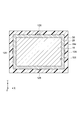
- FIG. 4 is a cross-sectional view of the power storage device along the line IV-IV in FIG.
- the welded portion 128 is disposed so as to surround the entire circumference of the outer peripheral portion 161 of the current collector 16 when viewed from the Z-axis direction.
- the welding part 128 is cylindrical.
- FIG. 5 shows, seeing from the Z-axis direction, the welding part 128 may be arrange
- the plurality of welded portions 128 are arranged apart from each other.
- Each welding part 128 is rod-shaped.
- the welded portion 128 is disposed, for example, at the center of each side of the current collector 16.
- the welding part 128 may be arrange
- the resin members 28 of the bipolar electrodes 12 adjacent in the Z-axis direction are connected to each other by the welded portion 128. Therefore, for example, when the insulating case 30 is formed by injection molding (insert molding), for example, even if a pressure in the lateral direction (in the XY plane) is applied to the bipolar electrode 12 by the fluid of the material of the insulating case 30, for example, The positional deviation between the matching bipolar electrodes 12 can be suppressed. When the number of stacked bipolar electrodes 12 is increased or the thickness of the bipolar electrode 12 is decreased, the positional deviation between the adjacent bipolar electrodes tends to be large.
- the power storage device 10 can suppress misalignment between adjacent bipolar electrodes 12. By suppressing misalignment between the adjacent bipolar electrodes, short circuit due to contact between the adjacent bipolar electrodes, poor dimension of the bipolar electrode, misalignment of the internal space in the insulating case 30, and the like are suppressed.
- the welded portion 128 when the welded portion 128 is disposed on each side of the current collector 16 having a rectangular shape when viewed from the Z-axis direction, the welded portion 128 is placed at each vertex of the current collector 16. Compared with the case where it arrange
- FIG. 6 is an enlarged cross-sectional view of the first resin member (resin member 29), the second resin member (insulating case 31), and the welded portion 129 according to such a modification.
- the resin members 29 of the bipolar electrodes 12 adjacent in the Z-axis direction are in contact with each other.
- the resin member 29 has a contact surface 29 c on the side opposite to the contact surface 29 a that contacts the first surface 16 a of the current collector 16, and contacts the second surface 16 b of the current collector 16.
- a contact surface 29d is provided on the side opposite to the contact surface 29b.
- the contact surface 29c of the resin member 29 is in contact with the contact surface 29d of the resin member 29 below (in the negative Z-axis direction).
- the contact surface 29d of the resin member 29 is in contact with the upper contact surface 29c of the resin member 29 (Z-axis positive direction).
- the separator 14 is located inside the resin member 29 when viewed from the Z-axis direction.
- the contact surface 29 c of the resin member 29 is located at the center of the separator 14 below the current collector 16 provided with the resin member 29 in the Z-axis direction.
- the contact surface 29 d of the resin member 29 is located at the center of the separator 14 above the current collector 16 provided with the resin member 29.
- the insulating case 31 is shaped to match the shape of the resin member 29, and does not have a portion located between the resin members 29 adjacent in the Z-axis direction as compared to the insulating case 30 (FIG. 3). Is different.
- the thickness of the resin member 29 is larger than any of the thickness of the positive electrode layer 18 and the thickness of the negative electrode layer 20.
- the resin member 29 is provided on both the first surface 16 a and the second surface 16 b of the current collector 16
- the resin member 29 is provided on the first surface 16 a of the current collector 16.
- the thickness of the provided portion (the length in the Z-axis direction) is larger than the thickness of the negative electrode layer 20.
- the thickness of the portion provided on the second surface 16 b of the current collector 16 is larger than the thickness of the positive electrode layer 18.
- the thickness of the resin member 29 may be larger than any of the thickness of the positive electrode layer 18 and the thickness of the negative electrode layer 20. Thereby, the space
- the resin members 29 of the bipolar electrodes 12 adjacent in the Z-axis direction may be in contact with each other. Thereby, the distance between the current collectors 16 can be determined using the thickness of the resin member 29.
- the welded portion 129 fixes the resin members 29 of the bipolar electrodes 12 adjacent in the Z-axis direction.
- the welded portion 129 is provided on the end surface 29e located outside the resin member 29 when viewed from the Z-axis direction.
- the end surface 29e connects the contact surface 29c and the contact surface 29d.
- the welded portion 129 extends from the bipolar electrode 12 at one end to the bipolar electrode 12 at the other end in the Z-axis direction.
- the welded portion 129 can be formed by the same method as the welded portion 128.
- the welding part 129 may be arrange
- An example of the material of the welded portion 129 is the same as the material of the welded portion 128.
- FIGS. 7 to 9 are cross-sectional views illustrating one process of the method for manufacturing the power storage device according to the embodiment.
- the first resin member, the second resin member, and the welded portion are the resin member 29, the insulating case 31, and the welded portion 129 shown in FIG. 6 described above will be described.
- Each of the plurality of bipolar electrodes 12 includes a current collector 16, a positive electrode layer 18, and a negative electrode layer 20.
- the resin member 29 is provided on the outer peripheral portion 161 (see FIG. 6) of the current collector 16.
- the resin member 29 may be provided on both the first surface 16 a and the second surface 16 b of the current collector 16 over the entire outer peripheral portion 161.
- the resin member 29 is formed by injection molding so that the resin member 29 covers the outer peripheral portion 161 of the current collector 16. Thereby, the current collector 16 and the resin member 29 are welded.
- a plurality of bipolar electrodes 12 are stacked in series via a separator 14.
- the resin members 29 of the bipolar electrodes 12 adjacent in the lamination direction of the plurality of bipolar electrodes 12 are in contact with each other.
- the separator 14 is provided so as to be positioned inside the resin member 29 when viewed from the stacking direction (Z-axis direction) of the plurality of bipolar electrodes 12.
- the resin members 29 of the bipolar electrodes 12 adjacent in the stacking direction of the plurality of bipolar electrodes 12 are connected by a welded portion 129. That is, the adjacent resin members 29 are welded together.
- the welding part 129 is formed by heating the end surface 29e (refer FIG. 6) of the resin member 29. FIG. Thereby, the adjacent resin members 29 are fixed to each other.
- the welding part 129 is formed by irradiating the end surface 29e of the resin member 29 with an ultrasonic wave, a laser, etc., for example.
- the insulating case 31 is provided on the resin members 29 connected to each other by the welded portion 129.
- the insulating case 31 is formed by injection molding using a mold M.
- a plurality of bipolar electrodes 12 connected to each other by the welded portion 129 are arranged in the mold M.
- the material fluid of the insulating case 31 is supplied into the mold M, and the material is solidified.
- the insulating case 31 supports the outer peripheral portion of the current collector 16 through the resin member 29.
- the plurality of bipolar electrodes 12, the plurality of separators 14, the electrodes 112, the electrodes 212, and the insulating case 31 are sandwiched by the positive electrode plate 40 and the negative electrode plate 50. Further, a binding force is applied to the positive electrode plate 40 and the negative electrode plate 50 using the bolt B and the nut N. Thereby, the electrical storage apparatus 10 is manufactured.
- the electrical storage apparatus 10 is manufactured by the method similar to the manufacturing method mentioned above. Can be manufactured.
- the resin member 29 after providing the resin member 29 on at least one of the first surface 16 a and the second surface 16 b in at least a part of the outer peripheral portion 161 of the current collector 16.
- a plurality of bipolar electrodes 12 are stacked. Thereby, when laminating
- the resin members 29 of the bipolar electrodes 12 adjacent in the stacking direction of the plurality of bipolar electrodes 12 are connected to each other by the welded portion 129. Therefore, for example, when forming the insulating case 31 by injection molding, even if a lateral pressure is applied to the bipolar electrode 12 by the fluid of the material of the insulating case 31, for example, it is possible to suppress the positional deviation between the adjacent bipolar electrodes 12. .
- the resin member 29 may be provided on both the first surface 16a and the second surface 16b.
- a plurality of bipolar electrodes 12 are stacked via the separators 14, and the resin members 29 of the bipolar electrodes 12 adjacent in the stacking direction of the plurality of bipolar electrodes 12 are in contact with each other.
- the separator 14 may be located inside the resin member 29 when viewed from the stacking direction. In this case, since the resin members 29 of the bipolar electrodes 12 adjacent in the stacking direction are in contact with each other, the distance between the current collectors 16 can be determined using the thickness of the resin member 29. Further, since the separator 14 is positioned inside the resin member 29 when viewed from the stacking direction, the separator 14 can be positioned using the resin member 29.
- the current collector 16 when viewed from the stacking direction of the plurality of bipolar electrodes 12, the current collector 16 may have a shape such as a polygon or a circle.
- the welded portion 128 or the welded portion 129 may be disposed on at least a part of the outer peripheral portion 161 of the current collector 16.
- the welded portion 128 may be disposed between the adjacent resin members 28 in the Z-axis direction instead of the end face 28e of the resin member 28.
- the welded portion 129 may be disposed between the adjacent resin members 29 in the Z-axis direction instead of the end surface 29e of the resin member 29.
- SYMBOLS 10 Power storage device, 12 ... Bipolar electrode, 14 ... Separator, 16 ... Current collector, 16a ... First surface, 16b ... Second surface, 18 ... Positive electrode layer, 20 ... Negative electrode layer, 28, 29 ... Resin member (First resin member), 30, 31 ... insulating case (second resin member), 128, 129 ... welded part, 161 ... outer peripheral part.
Landscapes
- Engineering & Computer Science (AREA)
- Power Engineering (AREA)
- Chemical & Material Sciences (AREA)
- Chemical Kinetics & Catalysis (AREA)
- Electrochemistry (AREA)
- General Chemical & Material Sciences (AREA)
- Microelectronics & Electronic Packaging (AREA)
- Manufacturing & Machinery (AREA)
- Materials Engineering (AREA)
- Secondary Cells (AREA)
- Electric Double-Layer Capacitors Or The Like (AREA)
- Sealing Battery Cases Or Jackets (AREA)
- Cell Electrode Carriers And Collectors (AREA)
- Connection Of Batteries Or Terminals (AREA)
Priority Applications (3)
| Application Number | Priority Date | Filing Date | Title |
|---|---|---|---|
| US16/325,488 US11735743B2 (en) | 2016-10-17 | 2017-09-21 | Power storage device and power storage device production method |
| CN201780062803.1A CN109891651B (zh) | 2016-10-17 | 2017-09-21 | 蓄电装置和蓄电装置的制造方法 |
| DE112017005247.5T DE112017005247B4 (de) | 2016-10-17 | 2017-09-21 | Energiespeichervorrichtung und Herstellungsverfahren einer Energiespeichervorrichtung |
Applications Claiming Priority (2)
| Application Number | Priority Date | Filing Date | Title |
|---|---|---|---|
| JP2016203570A JP6705358B2 (ja) | 2016-10-17 | 2016-10-17 | 蓄電装置の製造方法 |
| JP2016-203570 | 2016-10-17 |
Publications (1)
| Publication Number | Publication Date |
|---|---|
| WO2018074135A1 true WO2018074135A1 (ja) | 2018-04-26 |
Family
ID=62019357
Family Applications (1)
| Application Number | Title | Priority Date | Filing Date |
|---|---|---|---|
| PCT/JP2017/034103 Ceased WO2018074135A1 (ja) | 2016-10-17 | 2017-09-21 | 蓄電装置及び蓄電装置の製造方法 |
Country Status (5)
| Country | Link |
|---|---|
| US (1) | US11735743B2 (enExample) |
| JP (1) | JP6705358B2 (enExample) |
| CN (1) | CN109891651B (enExample) |
| DE (1) | DE112017005247B4 (enExample) |
| WO (1) | WO2018074135A1 (enExample) |
Cited By (3)
| Publication number | Priority date | Publication date | Assignee | Title |
|---|---|---|---|---|
| WO2019171698A1 (ja) * | 2018-03-09 | 2019-09-12 | 株式会社豊田自動織機 | 蓄電装置 |
| US20200358050A1 (en) * | 2018-01-30 | 2020-11-12 | Kabushiki Kaisha Toyota Jidoshokki | Power storage module and method for manufacturing power storage module |
| EP4418351A4 (en) * | 2021-12-02 | 2025-07-09 | Toyota Jidoshokki Kk | ELECTRODE UNIT MANUFACTURING DEVICE AND ELECTRODE UNIT MANUFACTURING METHOD |
Families Citing this family (5)
| Publication number | Priority date | Publication date | Assignee | Title |
|---|---|---|---|---|
| JP7102911B2 (ja) * | 2018-04-27 | 2022-07-20 | 株式会社豊田自動織機 | 蓄電モジュールの製造方法 |
| JP7188062B2 (ja) * | 2018-12-25 | 2022-12-13 | 株式会社豊田自動織機 | 蓄電モジュールの製造装置及び製造方法 |
| MX2023001847A (es) * | 2020-08-28 | 2023-04-27 | Eos Energy Tech Holdings Llc | Conjunto de terminales y elemento de bastidor de bateria para bateria recargable. |
| KR20240151800A (ko) * | 2022-05-11 | 2024-10-18 | 가부시키가이샤 도요다 지도숏키 | 축전 장치 |
| DE102022112678B3 (de) | 2022-05-20 | 2023-08-17 | Dr. Ing. H.C. F. Porsche Aktiengesellschaft | Vorrichtung und Verfahren zur thermischen Isolierung bei Zellstapeln |
Citations (6)
| Publication number | Priority date | Publication date | Assignee | Title |
|---|---|---|---|---|
| US4275130A (en) * | 1979-09-27 | 1981-06-23 | California Institute Of Technology | Bipolar battery construction |
| JPH01195673A (ja) * | 1988-01-29 | 1989-08-07 | Shin Kobe Electric Mach Co Ltd | 電池 |
| JPH0757768A (ja) * | 1993-06-21 | 1995-03-03 | General Motors Corp <Gm> | 二極バッテリー、その組立て方法及びハウジング形成方法 |
| JP2005190713A (ja) * | 2003-12-24 | 2005-07-14 | Nissan Motor Co Ltd | バイポーラ電池およびその製造方法。 |
| JP2006508518A (ja) * | 2002-11-29 | 2006-03-09 | ナイラー インターナショナル アーベー | バイポーラ電池およびその製造方法 |
| JP2014529175A (ja) * | 2011-09-09 | 2014-10-30 | イースト ペン マニュファクチャリング カンパニー インコーポレーテッドEast Penn Manufacturing Co.,Inc. | 二極式電池およびプレート |
Family Cites Families (20)
| Publication number | Priority date | Publication date | Assignee | Title |
|---|---|---|---|---|
| US5098801A (en) * | 1990-09-12 | 1992-03-24 | General Motors Corporation | Bipolar battery and assembly method |
| US5428501A (en) * | 1993-08-13 | 1995-06-27 | Marine Mechanical Corporation | Packaging structure and method for solid electrolyte capacitors |
| JP3070474B2 (ja) * | 1996-03-28 | 2000-07-31 | 日本電気株式会社 | 電気二重層コンデンサ及びその製造方法 |
| JP4122647B2 (ja) * | 1999-09-09 | 2008-07-23 | 株式会社明電舎 | 電気二重層キャパシタ及びその製造方法 |
| JP2001155973A (ja) | 1999-11-30 | 2001-06-08 | Meidensha Corp | 電気二重層キャパシタ |
| CN1254871C (zh) * | 2001-08-06 | 2006-05-03 | 松下电器产业株式会社 | 矩形密闭式电池 |
| JP4570863B2 (ja) | 2003-10-30 | 2010-10-27 | 川崎重工業株式会社 | バイポーラプレート方式の積層電池 |
| US8076021B2 (en) | 2004-12-10 | 2011-12-13 | Nissan Motor Co., Ltd. | Bipolar battery |
| US20090053601A1 (en) * | 2005-03-31 | 2009-02-26 | Kelley Kurtis C | Modular Bipolar Battery |
| GB0509753D0 (en) * | 2005-04-27 | 2005-06-22 | Atraverda Ltd | Electrode and manufacturing methods |
| JP2007087743A (ja) * | 2005-09-21 | 2007-04-05 | Dainippon Printing Co Ltd | インモールドラベルおよびそれを用いた蓄電池用包装容器 |
| WO2008114738A1 (ja) * | 2007-03-15 | 2008-09-25 | Gs Yuasa Corporation | 鉛蓄電池および組電池 |
| JP5458605B2 (ja) * | 2009-03-05 | 2014-04-02 | 日産自動車株式会社 | 双極型二次電池 |
| JP5333576B2 (ja) * | 2009-03-05 | 2013-11-06 | 日産自動車株式会社 | 双極型二次電池及びその製造方法 |
| JP2011023191A (ja) * | 2009-07-15 | 2011-02-03 | Nissan Motor Co Ltd | 双極型二次電池 |
| KR101322584B1 (ko) * | 2010-01-29 | 2013-10-28 | 닛산 지도우샤 가부시키가이샤 | 쌍극형 리튬 이온 2차 전지용 집전체 |
| KR101209461B1 (ko) * | 2010-02-01 | 2012-12-07 | 주식회사 엘지화학 | 신규한 구조의 전지셀 접합체 및 이를 포함하는 전지팩 |
| WO2012164642A1 (ja) * | 2011-05-27 | 2012-12-06 | トヨタ自動車株式会社 | バイポーラ全固体電池 |
| KR102014669B1 (ko) * | 2011-10-24 | 2019-08-26 | 어드밴스드 배터리 컨셉츠, 엘엘씨 | 바이폴라 배터리 조립체 |
| US9685677B2 (en) * | 2011-10-24 | 2017-06-20 | Advanced Battery Concepts, LLC | Bipolar battery assembly |
-
2016
- 2016-10-17 JP JP2016203570A patent/JP6705358B2/ja active Active
-
2017
- 2017-09-21 US US16/325,488 patent/US11735743B2/en active Active
- 2017-09-21 DE DE112017005247.5T patent/DE112017005247B4/de active Active
- 2017-09-21 WO PCT/JP2017/034103 patent/WO2018074135A1/ja not_active Ceased
- 2017-09-21 CN CN201780062803.1A patent/CN109891651B/zh active Active
Patent Citations (6)
| Publication number | Priority date | Publication date | Assignee | Title |
|---|---|---|---|---|
| US4275130A (en) * | 1979-09-27 | 1981-06-23 | California Institute Of Technology | Bipolar battery construction |
| JPH01195673A (ja) * | 1988-01-29 | 1989-08-07 | Shin Kobe Electric Mach Co Ltd | 電池 |
| JPH0757768A (ja) * | 1993-06-21 | 1995-03-03 | General Motors Corp <Gm> | 二極バッテリー、その組立て方法及びハウジング形成方法 |
| JP2006508518A (ja) * | 2002-11-29 | 2006-03-09 | ナイラー インターナショナル アーベー | バイポーラ電池およびその製造方法 |
| JP2005190713A (ja) * | 2003-12-24 | 2005-07-14 | Nissan Motor Co Ltd | バイポーラ電池およびその製造方法。 |
| JP2014529175A (ja) * | 2011-09-09 | 2014-10-30 | イースト ペン マニュファクチャリング カンパニー インコーポレーテッドEast Penn Manufacturing Co.,Inc. | 二極式電池およびプレート |
Cited By (4)
| Publication number | Priority date | Publication date | Assignee | Title |
|---|---|---|---|---|
| US20200358050A1 (en) * | 2018-01-30 | 2020-11-12 | Kabushiki Kaisha Toyota Jidoshokki | Power storage module and method for manufacturing power storage module |
| US11955593B2 (en) * | 2018-01-30 | 2024-04-09 | Kabushiki Kaisha Toyota Jidoshokki | Power storage module and method for manufacturing power storage module |
| WO2019171698A1 (ja) * | 2018-03-09 | 2019-09-12 | 株式会社豊田自動織機 | 蓄電装置 |
| EP4418351A4 (en) * | 2021-12-02 | 2025-07-09 | Toyota Jidoshokki Kk | ELECTRODE UNIT MANUFACTURING DEVICE AND ELECTRODE UNIT MANUFACTURING METHOD |
Also Published As
| Publication number | Publication date |
|---|---|
| JP2018067381A (ja) | 2018-04-26 |
| CN109891651B (zh) | 2022-12-13 |
| US11735743B2 (en) | 2023-08-22 |
| JP6705358B2 (ja) | 2020-06-03 |
| DE112017005247B4 (de) | 2023-05-11 |
| DE112017005247T5 (de) | 2019-07-11 |
| US20190260034A1 (en) | 2019-08-22 |
| CN109891651A (zh) | 2019-06-14 |
Similar Documents
| Publication | Publication Date | Title |
|---|---|---|
| JP6705358B2 (ja) | 蓄電装置の製造方法 | |
| JP6780345B2 (ja) | 蓄電装置及び蓄電装置の製造方法 | |
| JP6070552B2 (ja) | 蓄電デバイスの製造方法 | |
| JP6586969B2 (ja) | 蓄電モジュール | |
| US10141560B2 (en) | Energy storage device including a pressing member pressing a separator toward an electrode assembly | |
| JP6729137B2 (ja) | 二次電池及びその製造方法、並びにそれを用いた組電池 | |
| WO2019181501A1 (ja) | 蓄電装置 | |
| JP2011113970A (ja) | 二次電池 | |
| JP2019061779A (ja) | 蓄電装置及び蓄電装置の製造方法 | |
| CN107154312B (zh) | 电化学器件和电化学器件的制造方法 | |
| JP2018060670A (ja) | 蓄電装置 | |
| JP6476746B2 (ja) | 蓄電素子、電源モジュール及び蓄電素子の製造方法 | |
| JP6838640B2 (ja) | 蓄電装置 | |
| WO2018123503A1 (ja) | 蓄電モジュール及び蓄電モジュールの製造方法 | |
| JP2018018666A (ja) | 蓄電装置及び蓄電装置の製造方法 | |
| WO2018123502A1 (ja) | 蓄電モジュール及び蓄電モジュールの製造方法 | |
| JP2019067544A (ja) | 二次電池及びその製造方法 | |
| US11335956B2 (en) | Energy storage device and method of manufacturing energy storage device | |
| US12444798B2 (en) | Power storage device | |
| JP5501270B2 (ja) | 塗布型電極群を用いた電池 | |
| JP2018067382A (ja) | 蓄電装置 | |
| JP2020170667A (ja) | 積層型電池の製造方法および積層型電池 | |
| JP2024011384A (ja) | 電池 | |
| JP5423431B2 (ja) | 蓄電モジュールの連結構造及び蓄電モジュールの製造方法 | |
| JP2023038811A (ja) | 蓄電素子 |
Legal Events
| Date | Code | Title | Description |
|---|---|---|---|
| 121 | Ep: the epo has been informed by wipo that ep was designated in this application |
Ref document number: 17861421 Country of ref document: EP Kind code of ref document: A1 |
|
| 122 | Ep: pct application non-entry in european phase |
Ref document number: 17861421 Country of ref document: EP Kind code of ref document: A1 |