WO2018047717A1 - 半導体発光素子およびそれを含む発光装置 - Google Patents
半導体発光素子およびそれを含む発光装置 Download PDFInfo
- Publication number
- WO2018047717A1 WO2018047717A1 PCT/JP2017/031466 JP2017031466W WO2018047717A1 WO 2018047717 A1 WO2018047717 A1 WO 2018047717A1 JP 2017031466 W JP2017031466 W JP 2017031466W WO 2018047717 A1 WO2018047717 A1 WO 2018047717A1
- Authority
- WO
- WIPO (PCT)
- Prior art keywords
- layer
- refractive index
- axis
- light emitting
- region
- Prior art date
- Legal status (The legal status is an assumption and is not a legal conclusion. Google has not performed a legal analysis and makes no representation as to the accuracy of the status listed.)
- Ceased
Links
Images














Classifications
-
- H—ELECTRICITY
- H01—ELECTRIC ELEMENTS
- H01S—DEVICES USING THE PROCESS OF LIGHT AMPLIFICATION BY STIMULATED EMISSION OF RADIATION [LASER] TO AMPLIFY OR GENERATE LIGHT; DEVICES USING STIMULATED EMISSION OF ELECTROMAGNETIC RADIATION IN WAVE RANGES OTHER THAN OPTICAL
- H01S5/00—Semiconductor lasers
- H01S5/10—Construction or shape of the optical resonator, e.g. extended or external cavity, coupled cavities, bent-guide, varying width, thickness or composition of the active region
- H01S5/18—Surface-emitting [SE] lasers, e.g. having both horizontal and vertical cavities
- H01S5/183—Surface-emitting [SE] lasers, e.g. having both horizontal and vertical cavities having only vertical cavities, e.g. vertical cavity surface-emitting lasers [VCSEL]
-
- H—ELECTRICITY
- H01—ELECTRIC ELEMENTS
- H01S—DEVICES USING THE PROCESS OF LIGHT AMPLIFICATION BY STIMULATED EMISSION OF RADIATION [LASER] TO AMPLIFY OR GENERATE LIGHT; DEVICES USING STIMULATED EMISSION OF ELECTROMAGNETIC RADIATION IN WAVE RANGES OTHER THAN OPTICAL
- H01S5/00—Semiconductor lasers
- H01S5/02—Structural details or components not essential to laser action
- H01S5/028—Coatings ; Treatment of the laser facets, e.g. etching, passivation layers or reflecting layers
- H01S5/0287—Facet reflectivity
-
- H—ELECTRICITY
- H01—ELECTRIC ELEMENTS
- H01S—DEVICES USING THE PROCESS OF LIGHT AMPLIFICATION BY STIMULATED EMISSION OF RADIATION [LASER] TO AMPLIFY OR GENERATE LIGHT; DEVICES USING STIMULATED EMISSION OF ELECTROMAGNETIC RADIATION IN WAVE RANGES OTHER THAN OPTICAL
- H01S5/00—Semiconductor lasers
- H01S5/04—Processes or apparatus for excitation, e.g. pumping, e.g. by electron beams
- H01S5/042—Electrical excitation ; Circuits therefor
- H01S5/0425—Electrodes, e.g. characterised by the structure
- H01S5/04256—Electrodes, e.g. characterised by the structure characterised by the configuration
-
- H—ELECTRICITY
- H01—ELECTRIC ELEMENTS
- H01S—DEVICES USING THE PROCESS OF LIGHT AMPLIFICATION BY STIMULATED EMISSION OF RADIATION [LASER] TO AMPLIFY OR GENERATE LIGHT; DEVICES USING STIMULATED EMISSION OF ELECTROMAGNETIC RADIATION IN WAVE RANGES OTHER THAN OPTICAL
- H01S5/00—Semiconductor lasers
- H01S5/10—Construction or shape of the optical resonator, e.g. extended or external cavity, coupled cavities, bent-guide, varying width, thickness or composition of the active region
- H01S5/1082—Construction or shape of the optical resonator, e.g. extended or external cavity, coupled cavities, bent-guide, varying width, thickness or composition of the active region with a special facet structure, e.g. structured, non planar, oblique
- H01S5/1085—Oblique facets
-
- H—ELECTRICITY
- H01—ELECTRIC ELEMENTS
- H01S—DEVICES USING THE PROCESS OF LIGHT AMPLIFICATION BY STIMULATED EMISSION OF RADIATION [LASER] TO AMPLIFY OR GENERATE LIGHT; DEVICES USING STIMULATED EMISSION OF ELECTROMAGNETIC RADIATION IN WAVE RANGES OTHER THAN OPTICAL
- H01S5/00—Semiconductor lasers
- H01S5/10—Construction or shape of the optical resonator, e.g. extended or external cavity, coupled cavities, bent-guide, varying width, thickness or composition of the active region
- H01S5/11—Comprising a photonic bandgap structure
-
- H—ELECTRICITY
- H01—ELECTRIC ELEMENTS
- H01S—DEVICES USING THE PROCESS OF LIGHT AMPLIFICATION BY STIMULATED EMISSION OF RADIATION [LASER] TO AMPLIFY OR GENERATE LIGHT; DEVICES USING STIMULATED EMISSION OF ELECTROMAGNETIC RADIATION IN WAVE RANGES OTHER THAN OPTICAL
- H01S5/00—Semiconductor lasers
- H01S5/10—Construction or shape of the optical resonator, e.g. extended or external cavity, coupled cavities, bent-guide, varying width, thickness or composition of the active region
- H01S5/18—Surface-emitting [SE] lasers, e.g. having both horizontal and vertical cavities
-
- H—ELECTRICITY
- H01—ELECTRIC ELEMENTS
- H01S—DEVICES USING THE PROCESS OF LIGHT AMPLIFICATION BY STIMULATED EMISSION OF RADIATION [LASER] TO AMPLIFY OR GENERATE LIGHT; DEVICES USING STIMULATED EMISSION OF ELECTROMAGNETIC RADIATION IN WAVE RANGES OTHER THAN OPTICAL
- H01S5/00—Semiconductor lasers
- H01S5/10—Construction or shape of the optical resonator, e.g. extended or external cavity, coupled cavities, bent-guide, varying width, thickness or composition of the active region
- H01S5/18—Surface-emitting [SE] lasers, e.g. having both horizontal and vertical cavities
- H01S5/185—Surface-emitting [SE] lasers, e.g. having both horizontal and vertical cavities having only horizontal cavities, e.g. horizontal cavity surface-emitting lasers [HCSEL]
- H01S5/187—Surface-emitting [SE] lasers, e.g. having both horizontal and vertical cavities having only horizontal cavities, e.g. horizontal cavity surface-emitting lasers [HCSEL] using Bragg reflection
-
- H—ELECTRICITY
- H01—ELECTRIC ELEMENTS
- H01S—DEVICES USING THE PROCESS OF LIGHT AMPLIFICATION BY STIMULATED EMISSION OF RADIATION [LASER] TO AMPLIFY OR GENERATE LIGHT; DEVICES USING STIMULATED EMISSION OF ELECTROMAGNETIC RADIATION IN WAVE RANGES OTHER THAN OPTICAL
- H01S5/00—Semiconductor lasers
- H01S5/30—Structure or shape of the active region; Materials used for the active region
- H01S5/34—Structure or shape of the active region; Materials used for the active region comprising quantum well or superlattice structures, e.g. single quantum well [SQW] lasers, multiple quantum well [MQW] lasers or graded index separate confinement heterostructure [GRINSCH] lasers
- H01S5/343—Structure or shape of the active region; Materials used for the active region comprising quantum well or superlattice structures, e.g. single quantum well [SQW] lasers, multiple quantum well [MQW] lasers or graded index separate confinement heterostructure [GRINSCH] lasers in AIIIBV compounds, e.g. AlGaAs-laser, InP-based laser
- H01S5/34313—Structure or shape of the active region; Materials used for the active region comprising quantum well or superlattice structures, e.g. single quantum well [SQW] lasers, multiple quantum well [MQW] lasers or graded index separate confinement heterostructure [GRINSCH] lasers in AIIIBV compounds, e.g. AlGaAs-laser, InP-based laser with a well layer having only As as V-compound, e.g. AlGaAs, InGaAs
-
- H—ELECTRICITY
- H01—ELECTRIC ELEMENTS
- H01S—DEVICES USING THE PROCESS OF LIGHT AMPLIFICATION BY STIMULATED EMISSION OF RADIATION [LASER] TO AMPLIFY OR GENERATE LIGHT; DEVICES USING STIMULATED EMISSION OF ELECTROMAGNETIC RADIATION IN WAVE RANGES OTHER THAN OPTICAL
- H01S2301/00—Functional characteristics
- H01S2301/18—Semiconductor lasers with special structural design for influencing the near- or far-field
Definitions
- the present invention relates to a semiconductor light emitting element and a light emitting device including the same.
- the semiconductor light-emitting device described in Patent Document 1 includes an active layer, a pair of clad layers sandwiching the active layer, and a phase modulation layer optically coupled to the active layer.
- the phase modulation layer includes a basic layer and a plurality of different refractive index regions each having a refractive index different from the refractive index of the basic layer.
- each of the different refractive index regions main holes
- An auxiliary different refractive index region (sub-hole) is provided around the different refractive index region, and light having a predetermined beam pattern can be emitted.
- a semiconductor light emitting device that outputs an arbitrary optical image by controlling the phase spectrum and intensity spectrum of light emitted from a plurality of light emitting points arranged in a two-dimensional manner has been studied.
- a lower clad layer, an active layer, and an upper clad layer are provided on a semiconductor substrate, and between the lower clad layer and the active layer, or between the active layer and the upper clad layer.
- a phase modulation layer is provided therebetween.
- the phase modulation layer is composed of a basic layer and a plurality of different refractive index regions each having a refractive index different from the refractive index of the basic layer, and is virtual in a plane perpendicular to the thickness direction of the phase modulation layer.
- the barycentric positions of the different refractive index regions assigned to the plurality of square regions constituting the square lattice are the lattice point positions of the square regions assigned according to the optical image to be generated. It is off.
- Such a semiconductor light emitting device is called an S-iPM (Static-integrable Phase Modulating) laser, and has a direction perpendicular to the main surface of the semiconductor substrate (normal direction) and a predetermined spread angle with respect to the normal direction.
- a beam for forming a two-dimensional arbitrarily shaped optical image is output along the direction.
- the above-described semiconductor light-emitting element outputs 0th-order light in addition to signal light that is a desired output light image.
- This zero-order light is light that is output in a direction perpendicular to the main surface of the semiconductor substrate (that is, a direction perpendicular to light emission), and is not normally used in an SiPM laser. Accordingly, when obtaining a desired output light image, the 0th order light becomes noise light, and it is desired to remove the 0th order light from the optical image.
- the present invention has been made to solve the above-described problems, and a semiconductor light-emitting element having a structure capable of removing zero-order light from output light of an S-iPM laser and a light-emitting device including the same
- the purpose is to provide.
- the semiconductor light emitting device includes, as an example, an active layer, a pair of clad layers constituted by first and second clad layers, and a phase modulation layer.
- the semiconductor light emitting element has a light emitting surface and a light reflecting surface arranged opposite to the light emitting surface, and a normal direction of the light emitting surface and a predetermined inclination and spread with respect to the normal direction.
- An optical image having an arbitrary shape is output along an inclination direction having a corner.
- the active layer is disposed between the light emitting surface and the light reflecting surface.
- the first cladding layer is disposed between the light emitting surface and the active layer.
- the second cladding layer is disposed between the light reflecting surface and the active layer.
- the phase modulation layer is disposed between the first cladding layer and the active layer, or between the second cladding layer and the active layer.
- one of the first and second cladding layers has transmission characteristics with respect to the specific light image output along the tilt direction and reflects the 0th-order light output along the normal direction.
- a distributed Bragg reflective layer having characteristics is included.
- the phase modulation layer includes a basic layer and a plurality of different refractive index regions each having a refractive index different from the refractive index of the basic layer.
- the first step of providing a lower clad layer (second clad layer constituting a pair of clad layers) on the substrate and the active on the second clad layer A second step of providing a layer, a third step of providing an upper clad layer (a first clad layer constituting a pair of clad layers) on the active layer, and between the first step and the second step, or second
- the phase modulation layer is configured such that each of the plurality of different refractive index regions is individually disposed at a specific position.
- a Z axis that coincides with the normal direction
- an XY plane that coincides with one surface of the phase modulation layer including a plurality of different refractive index regions and includes an X axis and a Y axis orthogonal to each other
- a virtual configuration composed of M1 (an integer greater than or equal to 1)
- ⁇ N1 an integer greater than or equal to 1) unit configuration regions R each having a square shape.
- the lattice point where the center of gravity G1 of the different refractive index region located in the unit configuration region R (x, y) is the center of the unit configuration region R (x, y).
- a vector away from O (x, y) and from the lattice point O (x, y) to the center of gravity G1 is To face a constant direction, the phase modulation layer is formed.
- zero-order light can be removed from the output of the S-iPM laser.
- (A) And (b) is a figure explaining the consideration point at the time of calculating
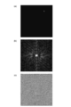
- (A) is an image of an original pattern common to three specific configurations of the phase modulation layer
- (b) is an image obtained by extracting the intensity distribution by two-dimensional Fourier transform of (a)
- ( c) shows a phase distribution extracted by performing two-dimensional Fourier transform on (a).
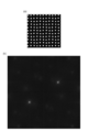
- (A) is an image showing the arrangement of the different refractive index regions in the phase modulation layer of the first configuration for realizing the phase distribution shown in FIG. 8 (c), and (b) is the different refractive index.
- (A) is an image showing the arrangement of the different refractive index regions in the phase modulation layer of the second configuration for realizing the phase distribution shown in FIG. 8 (c), and (b) is the different refractive index. This is an expected beam pattern obtained by Fourier transform of the entire region.
- (A) to (c) are images showing examples of beam patterns output from the laser element when it is assumed that there is no DBR layer. It is a figure which shows typically the cross-section of a laser element. It is a figure showing the specific structure of a DBR layer.
- FIG. 1 It is a figure which shows the structural model near a phase modulation layer and a DBR layer. It is a perspective view which shows the structure of the laser element which concerns on a 1st modification. It is a figure which shows the modification regarding arrangement
- (A)-(c) is a top view which shows the example of the shape in XY plane of a different refractive index area
- A) And (b) is a top view which shows the example of the shape in XY plane of a different refractive index area
- FIG. 31 is a graph showing a change in reflectance according to a change in incident angle in the p-type GaAs / AlGaAs layer of FIG. 30.
- FIG. 31 It is a graph which shows the refractive index distribution and electric field mode distribution of the laser element which were used when determining the structure of the p-type GaAs / AlGaAs layer as a DBR layer.
- the semiconductor light emitting device includes, as one aspect thereof, an active layer, a pair of clad layers composed of first and second clad layers, and a phase modulation layer, and a light emitting surface. And a light reflecting surface disposed opposite to the light emitting surface, and optionally along a normal direction of the light emitting surface and an inclined direction having a predetermined inclination and a spread angle with respect to the normal direction Outputs an optical image of a shape.
- the active layer is disposed between the light emitting surface and the light reflecting surface.
- the first cladding layer is disposed between the light emitting surface and the active layer.
- the second cladding layer is disposed between the light reflecting surface and the active layer.
- the phase modulation layer is disposed between the first cladding layer and the active layer, or between the second cladding layer and the active layer.
- one of the first and second cladding layers has transmission characteristics with respect to the specific light image output along the tilt direction and reflects the 0th-order light output along the normal direction.
- a distributed Bragg reflective layer having characteristics is included.
- the phase modulation layer includes a basic layer and a plurality of different refractive index regions each having a refractive index different from the refractive index of the basic layer.
- the first step of providing a lower clad layer (second clad layer constituting a pair of clad layers) on the substrate and the active on the second clad layer A second step of providing a layer, a third step of providing an upper clad layer (a first clad layer constituting a pair of clad layers) on the active layer, and between the first step and the second step, or second
- the phase modulation layer is configured such that each of the plurality of different refractive index regions is individually disposed at a specific position.
- a Z axis that coincides with the normal direction and an X axis and a Y axis that coincide with one surface of the phase modulation layer including a plurality of different refractive index regions are orthogonal to each other.
- the phase modulation layer is configured so that the vector from the lattice point O (x, y) to the center of gravity G1 is oriented in a specific direction.
- the distance between the distributed Bragg reflection layer and the phase modulation layer is set appropriately. Specifically, the distance between the distributed Bragg reflection layer and the phase modulation layer is determined by the components of the 0th order light that is reflected by the distributed Bragg reflection layer and then directed to the light exit surface, and the 0th order that is directly directed from the phase modulation layer to the light exit surface. The light components are set so as to weaken each other.
- the phase modulation layer optically coupled to the active layer is embedded in the basic layer, and the refractive index of the basic layer Has a plurality of different refractive index regions each having a different refractive index. Further, in the unit configuration region R (x, y) constituting the virtual square lattice, the centroid G1 of the corresponding different refractive index region is arranged away from the lattice point O (x, y). Furthermore, the direction of the vector from the lattice point O to the center of gravity G1 is individually set for each unit configuration region R.
- the phase of the beam changes depending on the direction of the vector from the lattice point O to the centroid G1 of the corresponding refractive index region, that is, the angular position around the lattice point of the centroid G1 of the different refractive index region.
- the phase of the beam output from each of the different refractive index regions can be controlled only by changing the position of the center of gravity of the different refractive index region, and the beam pattern formed as a whole It is possible to control (a beam group forming an optical image) to a desired shape.
- the lattice point in the virtual square lattice may be located outside the different refractive index region, or the lattice point may be located inside the different refractive index region.
- the semiconductor light emitting device applicable to this embodiment is a Si-PM laser, and has an arbitrary shape along the normal direction of the light emitting surface and the inclination direction having a predetermined inclination and spread angle with respect to the normal direction. (For example, a beam pattern formed on a two-dimensional plane) can be output.
- the distributed Bragg reflection layer has transmission characteristics with respect to a specific light image output along the tilt direction, while being output along the normal direction of the light exit surface. It is a layer having reflection characteristics with respect to light.
- the specific light image out of the light output from the phase modulation layer passes through the distributed Bragg reflection layer and easily reaches the light exit surface.
- the zero-order light is shielded by the distributed Bragg reflection layer, and it becomes difficult to reach the light exit surface. Therefore, according to the semiconductor light emitting device according to the present embodiment, the zero-order light can be suitably removed from the output of the semiconductor light emitting device.
- the distributed Bragg layer may be provided in the second cladding layer. That is, the distributed Bragg layer is located between the layer region formed of the active layer and the phase modulation layer and the light reflecting surface. In this case, it is important to set the distance between the distributed Bragg reflection layer and the phase modulation layer. Specifically, the distance between the distributed Bragg reflection layer and the phase modulation layer is determined by the components of the 0th order light that is reflected by the distributed Bragg reflection layer and then directed to the light exit surface, and the 0th order that is directly directed from the phase modulation layer to the light exit surface. The light components are set so as to weaken each other. Thereby, the specific light image of the light output from the phase modulation layer easily reaches the light exit surface.
- zero-order light can be suitably removed from the output of the semiconductor light emitting device.
- the lattice constant (substantially equivalent to the lattice spacing) of a virtual square lattice is a
- the different refractive index located in the unit constituent region R (x, y) The distance r between the center of gravity G1 of the region and the lattice point O (x, y) preferably satisfies 0 ⁇ r ⁇ 0.3a.
- an original image (light image before two-dimensional inverse Fourier return) expressed by a beam pattern emitted from a light emitting surface of a semiconductor light emitting element, for example, a spot, a straight line, a cross, a line drawing, a lattice pattern, a photograph And at least one of a striped pattern, computer graphics, and characters.
- the coordinates (x, y, z) in the XYZ orthogonal coordinate system are as shown in FIG.
- Spherical coordinates (d1, ⁇ tilt , ⁇ ) defined by the radial length d1, the tilt angle ⁇ tilt from the Z axis, and the rotation angle ⁇ rot from the X axis specified on the XY plane rot )) satisfy the relationships expressed by the following equations (1) to (3).
- FIG. 36 is a diagram for explaining coordinate conversion from spherical coordinates (d1, ⁇ tilt , ⁇ rot ) to coordinates (x, y, z) in the XYZ orthogonal coordinate system.
- z represents a designed optical image on a predetermined plane set in the XYZ orthogonal coordinate system which is a real space.
- the angle theta tilt and theta rot has the following formula (4)
- the coordinate value k x on the Kx axis corresponding to the X axis and the normalized wave number defined by the following equation (5), corresponding to the Y axis and on the Kx axis. shall be converted into coordinate values k y on Ky axis orthogonal.
- the normalized wave number means a wave number normalized with 1.0 as the wave number corresponding to the lattice spacing of a virtual square lattice.
- the specific wave number ranges including the beam pattern corresponding to the optical image are each square M2 (an integer of 1 or more) ⁇ N2 (an integer of 1 or more) ) Image regions FR.
- the integer M2 need not match the integer M1.
- the integer N2 need not match the integer N1.
- Y. Kurosaka et al. “Effects of non-lasing band in two-dimensional photonic-crystal lasers clarified using omnidirectional band structure,” Opt. Express 20, 21773 -21783 (2012).
- each region FR (k x, k y ) is identified by an X-axis coordinate component x (an integer between 1 and M1) and a Y-axis coordinate component y (an integer between 1 and N1) X ⁇
- the complex amplitude F (x, y) obtained by performing the two-dimensional inverse Fourier transform on the unit configuration region R (x, y) on the Y plane is given by the following formula (6), where j is an imaginary unit.
- the complex amplitude F (x, y) is defined by the following equation (7), where the amplitude term is A (x, y) and the phase term is P (x, y). Further, as a fourth precondition, the unit configuration region R (x, y) is parallel to the X axis and the Y axis, and is a lattice point O (x, y) that is the center of the unit configuration region R (x, y). It is defined by s-axis and t-axis that are orthogonal in y).
- the phase modulation layer is configured to satisfy the following first and second conditions. That is, the first condition is that any one of the plurality of different refractive index regions in the unit configuration region R (x, y) is in a state where the center of gravity G1 is separated from the lattice point O (x, y). It is arranged. Further, the second condition is common to each unit configuration region R in which the line segment length r (x, y) from the lattice point O (x, y) to the centroid G1 of the corresponding different refractive index region is M1 ⁇ N1.
- the corresponding different refractive index regions are arranged in the unit configuration region R (x, y) so as to satisfy the following relationship.
- the distance r between the center (lattice point) of each unit constituting region constituting the virtual square lattice and the centroid G1 of the corresponding different refractive index region. Is preferably a constant value over the entire phase modulation layer.
- the phase distribution in the entire phase modulation layer (the distribution of the phase term P (x, y) in the complex amplitude F (x, y) assigned to the unit configuration region R (x, y)) is 0 to 2 ⁇ (rad ),
- the center of gravity of the different refractive index region coincides with the lattice point of the unit constituent region R in the square lattice.
- the two-dimensional distributed Bragg diffraction effect in the above phase modulation layer is close to the two-dimensional distributed Bragg diffraction effect when the different refractive index region is arranged on each lattice point of the square lattice. Can be easily formed, and a reduction in threshold current for oscillation can be expected.
- the light emitting device may include, as one aspect thereof, a plurality of semiconductor light emitting elements each having a light emission surface and a drive circuit that individually drives the plurality of semiconductor light emitting elements.
- Each of the plurality of semiconductor light emitting elements has the above-described structure as the semiconductor light emitting element according to this embodiment.
- each of the plurality of semiconductor light emitting elements has a light emitting surface and a light reflecting surface arranged to face the light emitting surface, and the normal direction of the light emitting surface and the predetermined direction with respect to the normal direction An optical image having an arbitrary shape is output along the inclination direction having the inclination and the spread angle.
- each of the plurality of semiconductor light emitting elements includes an active layer, a pair of cladding layers sandwiching the active layer, and an optical layer provided between the active layer and one of the pair of cladding layers. And a phase modulation layer to be coupled.
- the pair of cladding layers includes a first cladding layer provided between the active layer and the light emitting surface, and a second cladding layer provided between the active layer and the light reflecting surface. It is composed of
- the phase modulation layer includes a basic layer and a plurality of different refractive index regions each having a refractive index different from the refractive index of the basic layer.
- the first cladding layer or the second cladding layer has transmission characteristics with respect to a specific light image output along the tilt direction, and with respect to zero-order light output along the normal direction.
- a distributed Bragg reflective layer having reflective characteristics.
- the phase modulation layer of each of the plurality of semiconductor light emitting elements is configured as follows. That is, in each of the plurality of semiconductor light emitting elements, the Z axis that coincides with the normal direction and the X axis that includes the X axis and the Y axis that are perpendicular to each other and coincide with one surface of the phase modulation layer including the plurality of different refractive index regions.
- M1 an integer of 1 or more
- N1 an integer of 1 or more unit configuration regions R each having a square shape on the XY plane. Is set to be a virtual square lattice.
- the unit configuration region R (on the XY plane) specified by the coordinate component x in the X-axis direction (an integer from 1 to M1) and the coordinate component y in the Y-axis direction (an integer from 1 to N1).
- the phase modulation layer is configured so that the vector is separated and the vector from the lattice point O (x, y) to the center of gravity G1 is directed in a specific direction.
- the light emitting device includes a plurality of semiconductor light emitting elements that are individually driven, and allows only a desired light image to be extracted from each of the semiconductor light emitting elements.
- a head-up display or the like can be suitably realized by appropriately driving necessary elements for a module in which semiconductor light emitting elements corresponding to a plurality of patterns are arranged in advance.
- each of the plurality of semiconductor light emitting devices includes a semiconductor light emitting device that outputs a light image in the red wavelength region, a semiconductor light emitting device that outputs a light image in the blue wavelength region, and a green wavelength region It is preferable to include any one of semiconductor light emitting elements that output a light image. In this case, a color head-up display can be suitably realized.
- each aspect listed in this [Description of Embodiments of the Invention] is applicable to each of all the remaining aspects or to all combinations of these remaining aspects. .
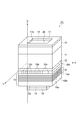
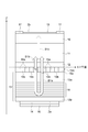
- FIG. 1 is a perspective view showing a configuration of a laser element 1A as an example of a semiconductor light emitting element according to this embodiment.
- an XYZ orthogonal coordinate system is defined in which the axis extending along the stacking direction (thickness direction) of the layers constituting the laser element 1A is the Z axis.
- the laser element 1A has a light reflecting surface 2a and a light emitting surface 2b that face each other in the Z direction.
- an XYZ orthogonal coordinate is obtained by an XY plane including an X axis and a Y axis orthogonal to each other, which is a plane orthogonal to the Z axis and coincides with one surface of the phase modulation layer 15A including the different refractive index region 15b.
- a system is defined.
- the laser element 1A is an S-iPM laser that forms a standing wave along the XY plane and outputs a phase-controlled plane wave in the Z-axis direction.
- the laser element 1A outputs a two-dimensional light image having an arbitrary shape along an inclination direction having a predetermined inclination and spread angle with respect to a direction perpendicular to the light emitting surface 2b (that is, the Z-axis direction).
- the laser element 1 ⁇ / b> A is provided on an active layer 12 provided on the semiconductor substrate 10, a pair of cladding layers 11 and 13 provided on the semiconductor substrate 10 and sandwiching the active layer 12, and a central region of the cladding layer 13.
- Contact layer 14 The semiconductor substrate 10, the active layer 12, the cladding layers 11 and 13, and the contact layer 14 are made of a compound semiconductor such as a GaAs-based semiconductor, an InP-based semiconductor, or a nitride-based semiconductor.
- the energy band gap of the cladding layer 11 and the energy band gap of the cladding layer 13 are larger than the energy band gap of the active layer 12.
- the thickness direction (stacking direction) of the semiconductor substrate 10, the active layer 12, the cladding layers 11 and 13, and the contact layer 14 coincides with the Z-axis direction.
- the laser element 1A further includes a phase modulation layer 15A.
- the phase modulation layer 15 ⁇ / b> A is provided between the active layer 12 and the cladding layer 13. Therefore, in the example of FIG. 1, the cladding layer (first cladding layer) 11 is positioned between the layer region and the light emitting surface 2b with reference to the layer region formed by the active layer 12 and the phase modulation layer 15A.
- the clad layer (second clad layer) 13 is positioned between the layer amount region and the light reflecting surface 2a.
- a light guide layer may be provided between at least one of the active layer 12 and the cladding layer 13 and between the active layer 12 and the cladding layer 11. When the light guide layer is provided between the active layer 12 and the clad layer 13, the phase modulation layer 15A is provided between the clad layer 13 and the light guide layer.
- the thickness direction of the phase modulation layer 15A coincides with the Z-axis direction.
- the phase modulation layer 15 ⁇ / b> A may be provided between the clad layer 11 and the active layer 12. Further, when the light guide layer is provided between the active layer 12 and the clad layer 11, the phase modulation layer 15 ⁇ / b> A is provided between the clad layer 11 and the light guide layer. Also in the example of FIG. 2, the clad layer (first clad layer) 11 is located between the layer region and the light emitting surface 2b with reference to the layer region constituted by the active layer 12 and the phase modulation layer 15A. The cladding layer (second cladding layer) 13 is located between the layer amount region and the light reflecting surface 2a.
- the phase modulation layer 15A is composed of a basic layer 15a made of a first refractive index medium and a second refractive index medium having a refractive index different from that of the first refractive index medium, and a plurality of different refractive index regions existing in the basic layer 15a. 15b.
- the plurality of different refractive index regions 15b include a structure in which the position of the center of gravity is shifted from the substantially periodic structure.
- the phase modulation layer (diffraction grating layer) 15A can select the wavelength ⁇ 0 of the emission wavelengths of the active layer 12 and output the light of the selected wavelength to the outside.
- the laser light incident on the phase modulation layer 15A forms a predetermined mode in accordance with the arrangement of the different refractive index regions 15b in the phase modulation layer 15A, and forms the surface of the laser element 1A (as a laser beam having a desired pattern). The light exits from the light exit surface 2b).
- the laser element 1 ⁇ / b> A further includes an electrode 16 provided on the contact layer 14 and an electrode 17 provided on the back surface of the semiconductor substrate 10.
- the electrode 16 is in ohmic contact with the contact layer 14, and the electrode 17 is in ohmic contact with the semiconductor substrate 10.
- the electrode 17 has a rectangular opening 17a.
- a portion other than the electrode 17 (including the inside of the opening 17 a) is covered with an antireflection film 19.
- the electrode 16 is made of, for example, Ti / Au, Ti / Pt / Au, or Cr / Au.
- the electrode 17 is made of, for example, AuGe / Au.
- the active layer 12 When a driving current is supplied between the electrode 16 and the electrode 17, recombination of electrons and holes occurs in the active layer 12 (light emission). The electrons and holes that contribute to this light emission and the generated light are efficiently confined between the cladding layer 11 and the cladding layer 13.
- the laser light emitted from the active layer 12 enters the phase modulation layer 15A and repeats scattering and diffraction to form a predetermined mode corresponding to the lattice structure inside the phase modulation layer 15A. A part of the laser light diffracted in the phase modulation layer 15A is reflected by the electrode 16 and emitted from the back surface of the semiconductor substrate 10 to the outside through the opening 17a.
- the remaining part of the laser beam incident on the phase modulation layer 15A directly reaches the back surface of the semiconductor substrate 10, and is emitted to the outside through the opening 17a from the back surface.
- the 0th-order light included in the laser light is emitted along the Z axis (normal direction of the light emitting surface 2b).
- the signal light included in the laser light is emitted along the Z-axis direction (normal direction) and a direction having a predetermined spread angle with respect to the normal direction. It is signal light that forms a desired light image (specific light image), and zero-order light is not used in this embodiment.
- the semiconductor substrate 10 is a GaAs substrate, and the cladding layer 11, the active layer 12, the phase modulation layer 15A, the cladding layer 13, and the contact layer 14 are made of group III elements Ga, Al, In, and group V elements, respectively. It is a compound semiconductor layer comprised by the element contained in the group which consists of As.
- the cladding layer 11 is an AlGaAs layer
- the active layer 12 has a multiple quantum well structure (barrier layer: AlGaAs / well layer: InGaAs), and the basic layer 15a of the phase modulation layer 15A is GaAs.
- the different refractive index region 15b is a hole
- the cladding layer 13 is an AlGaAs layer
- the contact layer 14 is a GaAs layer.
- the energy band gap and the refractive index can be easily changed by changing the Al composition ratio.
- Al X Ga 1-X As when the composition ratio X of Al having a relatively small atomic radius is decreased (increased), the energy band gap having a positive correlation with it decreases (increases). If InGaAs having a large atomic radius is mixed with GaAs to form InGaAs, the energy band gap is reduced. That is, the Al composition ratio of the cladding layers 11 and 13 is larger than the Al composition ratio of the barrier layer (AlGaAs) of the active layer 12.
- the Al composition ratio of the cladding layer 11 is set to 0.2 to 1.0, for example, and is 0.4 in one example.
- the Al composition ratio of the clad layer 13 is set to be the same as or higher than the Al composition of the clad layer 11, and is set to 0.2 to 1.0, for example, 0.7 in one example.
- the Al composition ratio of the barrier layer of the active layer 12 is set to be lower than the Al composition in the cladding layer, for example, set to 0.1 to 0.4, and is 0.15 in one example.
- the semiconductor substrate 10 is an InP substrate, and the cladding layer 11, the active layer 12, the phase modulation layer 15 ⁇ / b> A, the cladding layer 13, and the contact layer 14 include group III elements Ga, Al, In, and V It is composed of a compound semiconductor, for example, an InP-based compound semiconductor, that is not composed only of an element included in the group consisting of the group element As.
- the cladding layer 11 is an InP layer
- the active layer 12 has a multiple quantum well structure (barrier layer: GaInAsP / well layer: GaInAsP), and the basic layer 15a of the phase modulation layer 15A is made of GaInAsP.
- the different refractive index region 15b is a hole
- the cladding layer 13 is an InP layer
- the contact layer 14 is a GaInAsP layer.
- the semiconductor substrate 10 is a GaN substrate
- the cladding layer 11, the active layer 12, the phase modulation layer 15A, the cladding layer 13, and the contact layer 14 are group III elements Ga, Al, In, and V groups. It is a compound semiconductor layer that is not composed only of an element included in the group consisting of the element As, and is made of, for example, a nitride compound semiconductor.
- the cladding layer 11 is an AlGaN layer
- the active layer 12 has a multiple quantum well structure (barrier layer: InGaN / well layer: InGaN)
- the basic layer 15a of the phase modulation layer 15A is GaN.
- the different refractive index region 15b is a hole
- the cladding layer 13 is an AlGaN layer
- the contact layer 14 is a GaN layer.
- the clad layer 11 is given the same conductivity type as that of the semiconductor substrate 10, and the clad layer 13 and the contact layer 14 are given a conductivity type opposite to that of the semiconductor substrate 10.
- the semiconductor substrate 10 and the cladding layer 11 are n-type, and the cladding layer 13 and the contact layer 14 are p-type.
- the impurity concentration is, for example, 1 ⁇ 10 17 to 1 ⁇ 10 21 / cm 3 .
- the phase modulation layer 15A and the active layer 12 are intrinsic (i-type) to which neither impurity is intentionally added, and the impurity concentration thereof is 1 ⁇ 10 15 / cm 3 or less.
- the thickness of the substrate 10 is 100 to 600 ( ⁇ m), and in one example is 150 ( ⁇ m).
- the thickness of the clad layer 11 is 1 to 3 ( ⁇ m), and in an example is 2 ( ⁇ m).
- the thickness of the active layer 12 is 160 to 720 (nm), and in one example is 225 (nm).
- the thickness of the phase modulation layer 15A is 100 to 300 (nm), and in one example is 250 (nm).
- the thickness of the cladding layer 13 is 1 to 3 ( ⁇ m), and in an example is 2 ( ⁇ m).
- the contact layer 14 has a thickness of 50 to 190 (nm), and in one example is 100 (nm).
- the different refractive index region 15b is a hole.
- the different refractive index region 15b may be formed even if a semiconductor having a refractive index different from that of the basic layer 15a is embedded in the hole. Good.
- holes in the basic layer 15a may be formed by etching.
- the semiconductor may be embedded in the vacancies using metal organic vapor phase epitaxy, sputtering, or epitaxial methods.
- the basic layer 15a is made of GaAs
- the different refractive index region 15b may be made of AlGaAs.
- the different refractive index region 15b is formed by embedding a semiconductor in the holes of the basic layer 15a, the same semiconductor as the different refractive index region 15b may be further deposited thereon.
- region 15b is a void
- the antireflection film 19 is made of, for example, a dielectric single layer film such as silicon nitride (eg, SiN) or silicon oxide (eg, SiO 2 ), or a dielectric multilayer film.
- a dielectric single layer film such as silicon nitride (eg, SiN) or silicon oxide (eg, SiO 2 ), or a dielectric multilayer film.
- the dielectric multilayer film include titanium oxide (TiO 2 ), silicon dioxide (SiO 2 ), silicon monoxide (SiO), niobium oxide (Nb 2 O 5 ), tantalum pentoxide (Ta 2 O 5 ), fluorine, and the like.
- Dielectric layers such as magnesium oxide (MgF 2 ), titanium oxide (TiO 2 ), aluminum oxide (Al 2 O 3 ), cerium oxide (CeO 2 ), indium oxide (In 2 O 3 ), and zirconium oxide (ZrO 2 )
- MgF 2 magnesium oxide
- TiO 2 titanium oxide
- Al 2 O 3 aluminum oxide
- CeO 2 cerium oxide
- In 2 O 3 indium oxide
- ZrO 2 zirconium oxide
- the electrode shape can be deformed, and laser light can be emitted from the surface of the contact layer 14. That is, when the opening 17 a of the electrode 17 is not provided and the electrode 16 is opened on the surface of the contact layer 14, the laser beam is emitted from the surface of the contact layer 14 to the outside. In this case, the surface of the contact layer 14 becomes a light emitting surface, and the back surface of the semiconductor substrate 10 becomes a light reflecting surface.
- the antireflection film is provided in and around the opening of the electrode 16.
- FIG. 3 is a plan view of the phase modulation layer 15A.
- the phase modulation layer 15A includes a basic layer 15a made of a first refractive index medium and a different refractive index region 15b made of a second refractive index medium having a refractive index different from that of the first refractive index medium.
- a virtual square lattice in the XY plane is set in the phase modulation layer 15A.
- One side of the square lattice is parallel to the X axis, and the other side is parallel to the Y axis.
- the square unit constituting region R centering on the lattice point O of the square lattice can be set two-dimensionally over a plurality of columns along the X axis and a plurality of rows along the Y axis.
- the plurality of different refractive index regions 15b are provided one by one in each unit configuration region R.
- the planar shape of the different refractive index region 15b is, for example, a circular shape.
- the center of gravity G1 of the different refractive index region 15b is arranged away from the lattice point O that is closest thereto.
- the XY plane is a plane orthogonal to the thickness direction (Z axis) of the laser element 1A shown in FIGS.
- Each unit constituting region R constituting the square lattice is specified by a coordinate component x (an integer of 1 or more) in the X-axis direction and a coordinate component y (an integer of 1 or more) in the Y-axis direction, and the unit constituting region R (x , Y).
- the center of the unit configuration region R (x, y), that is, the lattice point is represented by O (x, y).
- the lattice point O may be located outside the different refractive index region 15b or may be included inside the different refractive index region 15b.
- the ratio of the area S of the different refractive index region 15b in one unit constituent region R is defined as a filling factor (FF).
- the area of one unit constituent region R is equal to the area in one unit lattice of a virtual square lattice.
- the unit constituting region R (x, y) constituting the square lattice is defined by the s axis and the t axis orthogonal to each other at the lattice point O (x, y).
- the s axis is an axis parallel to the X axis
- the t axis is an axis parallel to the Y axis.
- the rotation angle ⁇ (x, y) around the lattice point O (x, y) of the centroid G1 of the different refractive index region 15b becomes a desired optical image.
- the unit configuration area R is set independently.
- the rotation angle ⁇ (x, y) has a specific value in the unit configuration region R (x, y), but is not necessarily represented by a specific function. That is, the rotation angle ⁇ (x, y) is determined from the phase term of the complex amplitude obtained by converting a desired optical image onto the wave number space and performing a two-dimensional inverse Fourier transform on a certain wave number range of the wave number space.
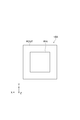
- FIG. 5 is a plan view showing an example in which the substantially periodic structure having the refractive index of FIG. 3 is applied only in a specific region of the phase modulation layer.
- a substantially periodic structure eg, the structure of FIG. 3 for emitting a target beam pattern is formed inside the square inner region RIN.
- the outer region ROUT surrounding the inner region RIN a true circular different refractive index region having a centroid position coincident with a lattice point position of a square lattice is arranged.
- the filling factor FF in the outer region ROUT is set to 12%.
- the outer region ROUT may be provided with a one-dimensional diffraction grating periodically arranged in a direction perpendicular to the side surrounding the inner region RIN.
- the current is supplied to the inner region RIN and not supplied to the outer region ROUT.
- it is possible to suppress the generation of high-frequency noise (so-called window function noise) caused by a rapid change in light intensity in the peripheral portion of the inner region RIN by distributing light also in the outer region ROUT.
- window function noise high-frequency noise
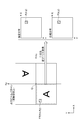
- FIG. 6 is a diagram for explaining the relationship between the optical image corresponding to the beam pattern output from the laser element 1A and the distribution of the rotation angle ⁇ (x, y) in the phase modulation layer 15A.
- the plane on which the optical image is formed by the beam emitted from the laser element 1A is wavenumber.
- the Kx-Ky plane obtained by transforming into space.
- the Kx axis and the Ky axis that define the Kx-Ky plane are orthogonal to each other, and the normal direction when the beam emission direction is swung from the Z-axis direction to the horizontal direction orthogonal to the Z-axis direction, respectively. Is associated with the angle by the above formulas (1) to (5).
- the specific area including the beam pattern corresponding to the optical image is composed of M2 (an integer greater than or equal to 1) ⁇ N2 (an integer greater than or equal to 1) image areas FR each having a square shape. Shall.
- a virtual square lattice set on the XY plane on the phase modulation layer 15A is composed of M1 (an integer of 1 or more) ⁇ N1 (an integer of 1 or more) unit configuration regions R.
- the integer M2 need not match the integer M1.
- the integer N2 need not match the integer N1.
- the image region FR in the Kx-Ky plane is specified by the coordinate component k x in the Kx axis direction (an integer of 1 to M2) and the coordinate component k y in the Ky axis direction (an integer of 1 to N2).
- Each of (k x , k y ) is a unit component region R identified by a coordinate component x in the X-axis direction (an integer from 1 to M1) and a coordinate component y in the Y-axis direction (an integer from 1 to N1).
- the complex amplitude F (x, y) in the unit configuration region R (x, y) obtained by two-dimensional inverse Fourier transform to (x, y) is given by the following equation (8), where j is an imaginary unit.
- the amplitude term in the complex amplitude F (x, y) of the unit configuration region R (x, y) is A ( The distribution of x, y) corresponds to the intensity distribution on the XY plane.
- the phase term in the complex amplitude F (x, y) of the unit configuration region R (x, y) is expressed as the distribution of P (x, y), Corresponds to the phase distribution on the -Y plane.
- the distribution of the rotation angle ⁇ (x, y) of the unit configuration region R (x, y) corresponds to the rotation angle distribution on the XY plane.
- the center Q of the output beam pattern on the Kx-Ky plane is located on an axis perpendicular to the main surface (light emitting surface 2b) of the semiconductor substrate 10, and in FIG. Four quadrants are shown.
- FIG. 6 as an example, a case where a light image is obtained in the first quadrant and the third quadrant is shown, but it is also possible to obtain images in the second quadrant and the fourth quadrant, or all quadrants.
- a light image that is point-symmetric with respect to the origin is obtained.
- FIG. 6 shows, as an example, a case where a character “A” is obtained in the third quadrant and a pattern obtained by rotating the character “A” 180 ° in the first quadrant is obtained.
- a rotationally symmetric optical image for example, a cross, a circle, a double circle, etc.
- they are overlapped and observed as one optical image.
- the beam pattern (light image) output from the laser element 1A is expressed by at least one of a spot, a straight line, a cross, a line drawing, a lattice pattern, a photograph, a striped pattern, CG (computer graphics), and characters.
- An optical image corresponding to the upper optical image (original image) is obtained.
- the rotation angle ⁇ (x, y) of the different refractive index region 15b in the unit configuration region R (x, y) is determined by the following procedure.
- the center of gravity G1 of the different refractive index region 15b is arranged in a state separated from the lattice point O (x, y) by r (x, y). .
- the different refractive index region 15b is arranged in the unit configuration region R (x, y) so that the rotation angle ⁇ (x, y) satisfies the following relationship.
- ⁇ (x, y) C ⁇ P (x, y) + B
- C proportional constant, for example 180 ° / ⁇ B: Arbitrary constant, for example 0
- the proportionality constant C and the arbitrary constant B are the same value for all unit constituent regions R.
- the optical image formed on the Kx-Ky plane projected onto the wave number space is converted into a unit configuration region R (x, y on the XY plane on the phase modulation layer 15A.
- the rotation angle ⁇ (x, y) corresponding to the phase term P (x, y) of the complex amplitude F (x, y) is converted into the unit configuration region R (x, y).
- the far-field image of the laser beam after the two-dimensional inverse Fourier transform can be a single or multiple spot shape, circular shape, linear shape, character shape, double annular shape, or Laguerre Gaussian beam shape.
- the shape can be taken. Since the beam pattern is represented by wave number information in the wave number space (on the Kx-Ky plane), in the case of a bitmap image or the like in which the target beam pattern is represented by two-dimensional position information In this case, it is preferable to perform two-dimensional inverse Fourier transform after first converting to wave number information.
- the intensity distribution (the amplitude term A (x, y) on the XY plane) Distribution
- the phase distribution (the distribution of the phase term P (x, y) on the XY plane) It can be calculated by using the angle function of MATLAB.
- the rotation angle distribution (distribution of the rotation angle ⁇ (x, y) on the XY plane) is obtained from the result of the two-dimensional inverse Fourier transform of the optical image, and the different refractive index regions 15b in the unit constituent regions R are obtained.
- the points to be noted when calculating using a general discrete two-dimensional inverse Fourier transform or high-speed two-dimensional inverse Fourier transform will be described.
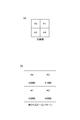
- An optical image before the two-dimensional inverse Fourier transform (designed optical image on a predetermined plane expressed by coordinates (x, y, z) in the XYZ orthogonal coordinate system) is an original image shown in FIG.
- the resulting beam pattern is the pattern shown in FIG. 7B. That is, in the first quadrant of the beam pattern of FIG. 7B, a pattern in which the pattern of the first quadrant of FIG. 7A rotated by 180 ° and the pattern of the third quadrant of FIG. . In the second quadrant of the beam pattern in FIG. 7B, a pattern in which the pattern obtained by rotating the second quadrant in FIG. 7A by 180 ° and the pattern in the fourth quadrant in FIG. In the third quadrant of the beam pattern of FIG. 7B, a pattern in which the pattern of the third quadrant of FIG. 7A rotated by 180 ° and the pattern of the first quadrant of FIG. In the fourth quadrant of the beam pattern in FIG. 7B, a pattern in which the pattern obtained by rotating the fourth quadrant in FIG. 7A by 180 ° and the pattern in the second quadrant in FIG.
- the first quadrant of the original optical image is included in the third quadrant of the obtained beam pattern.
- a quadrant pattern appears.
- a pattern obtained by rotating the first quadrant of the original optical image by 180 ° appears in the first quadrant of the obtained beam pattern.
- S is the area of the different refractive index region 15b in the XY plane.
- S ⁇ ⁇ (D / 2) 2 using the diameter D of the perfect circle.
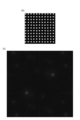
- FIG. 8A is an image of an original pattern common to each configuration, and is a character of “light” composed of 704 ⁇ 704 pixels. At this time, the characters “light” exist in the first quadrant, and no pattern exists in the second to fourth quadrants.
- FIG. 8B is an image obtained by extracting the intensity distribution by two-dimensional Fourier transform of FIG. 8A, and is composed of 704 ⁇ 704 elements.
- FIG. 8C is an image obtained by extracting the phase distribution by two-dimensional Fourier transform of FIG. 8A, and is composed of 704 ⁇ 704 elements. This also corresponds to the angular distribution.
- FIG. 8C shows the phase distribution of 0 to 2 ⁇ (rad) depending on the color density. The black part represents the phase 0 (rad).
- FIG. 9A is an image showing the arrangement of the different refractive index regions 15b in the phase modulation layer 15A having the first configuration for realizing the phase distribution shown in FIG. 8C.
- the basic layer 15a is shown in FIG. It is shown in black and the different refractive index region 15b is shown in white.
- this first configuration there are 704 ⁇ 704 different refractive index regions 15b, the planar shape of the different refractive index regions 15b is a perfect circle, and the lattice interval a of the square lattice is 284 nm.
- FIG. 9A shows a case where the diameter D of the different refractive index region 15b is 111 nm, and the distance r between the virtual square lattice point O and the center of gravity G1 of the different refractive index region 15b is 8.52 nm. At this time, the filling factor FF of the different refractive index region 15b is 12%, and the distance r is 0.03a.
- FIG. 9B shows an expected beam pattern obtained by performing Fourier transform on the entire different refractive index region.
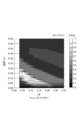
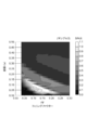
- FIG. 10 shows the S / N ratio of the output beam pattern, that is, the desired beam pattern and noise in accordance with the relationship between the filling factor FF and the distance r (a) in the first configuration (sample 1) of the phase modulation layer 15A. It is a graph which shows an intensity ratio.
- FIG. 11 is a graph showing the relationship between the distance r (a) and the S / N ratio in the case of FIG. 10 (sample 1 of the first configuration).
- the S / N increases.
- the distance r is preferably 0 ⁇ r ⁇ 0.3a, more preferably 0.01a ⁇ r ⁇ 0.3a, and further 0.03a ⁇ r ⁇ 0.25a. preferable.
- r is smaller than 0.01a, a beam pattern can be obtained with a small S / N ratio.
- FIG. 12A is an image (second configuration of the phase modulation layer 15A) showing an arrangement of the different refractive index regions 15b for realizing the phase distribution shown in FIG. It is shown in black and the different refractive index region 15b is shown in white.
- the planar shape of the different refractive index region 15b is square, and the number of the different refractive index regions 15b and the lattice spacing a of the square lattice are the same as those in the first configuration.
- the length L of one side of the different refractive index region 15b is 98.4 nm, and the distance r between the virtual square lattice point O and the center of gravity G1 of the different refractive index region 15b is 8.52 nm. Shows the case. At this time, the filling factor FF of the different refractive index region 15b is 12%, and the distance r is 0.03a.
- FIG. 12B shows an expected beam pattern obtained by performing Fourier transform on the entire different refractive index region.
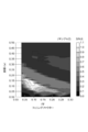
- FIG. 13 shows the S / N ratio of the output beam pattern, that is, the intensity of the desired beam pattern and noise in accordance with the relationship between the filling factor FF and the distance r (a) in the second configuration of the phase modulation layer (sample 2). It is a graph which shows ratio.
- FIG. 14 is a graph showing the relationship between the distance r (a) and the S / N ratio in the case of FIG. 13 (sample 2 of the second configuration). Even in this structure, at least when the distance r is 0.3a or less, the S / N is higher than when the distance r exceeds 0.3a, and when the distance r is 0.01a or more, it is 0. It turns out that S / N becomes higher than the case. In particular, referring to FIG.
- the distance r is preferably 0 ⁇ r ⁇ 0.3a, more preferably 0.01a ⁇ r ⁇ 0.3a, and further 0.03a ⁇ r ⁇ 0.25a. preferable.
- r is smaller than 0.01a, a beam pattern can be obtained with a small S / N ratio.
- FIG. 15A is an image (third configuration of the phase modulation layer 15A) showing the arrangement of the different refractive index regions 15b for realizing the phase distribution shown in FIG. 8C.
- the basic layer 15a is shown in FIG. It is shown in black and the different refractive index region 15b is shown in white.
- the planar shape of the different refractive index region 15b is a shape in which two perfect circles are shifted from each other and overlapped, and the center of gravity of one perfect circle is made coincident with the lattice point O.
- the number of different refractive index regions 15b and the lattice spacing a of the square lattice were the same as those in the first configuration.
- FIG. 9A shows a case where the diameters of two perfect circles are both 111 nm, and the distance r between the center of gravity of the other perfect circle and the lattice point O is 14.20 nm. At this time, the filling factor FF of the different refractive index region 15b is 12%, and the distance r is 0.05a.
- FIG. 15B shows an expected beam pattern obtained by performing Fourier transform on the entire different refractive index region.
- FIG. 16 shows the S / N ratio of the output beam pattern, that is, the desired beam pattern and noise in accordance with the relationship between the filling factor FF and the distance r (a) in the third configuration (sample 3) of the phase modulation layer 15A. It is a graph which shows an intensity ratio.
- FIG. 17 is a graph showing the relationship between the distance r (a) and the S / N ratio in the case of FIG. 16 (sample 3 of the third configuration). Even in this structure, at least when the distance r is 0.3a or less, the S / N is higher than when the distance r exceeds 0.3a, and when the distance r is 0.01a or more, it is 0. It turns out that S / N becomes higher than the case.
- the distance r is preferably 0 ⁇ r ⁇ 0.3a, more preferably 0.01a ⁇ r ⁇ 0.3a, and further 0.03a ⁇ r ⁇ 0.25a. preferable.
- r is smaller than 0.01a, a beam pattern can be obtained with a small S / N ratio.
- S / N is 0.6 or more) FF> 0.03 and r> 0.04 and r ⁇ (3/4) FF + 0.2375, and r> ⁇ FF + 0.15
- S / N is 0.3 or more) FF> 0.03 and r> 0.01 and r ⁇ (2/3) FF + 1/3 and r> ⁇ (2/3) FF + 0.10
- S / N is 0.9 or more) r> 0.025, and r> ⁇ (4/3) FF + 0.20 and r ⁇ (20/27) FF + 0.20 (In FIG.
- S / N is 0.6 or more) FF> 0.03 and r> 0.02 and r> ⁇ (5/4) FF + 0.1625, and r ⁇ -(13/18) FF + 0.222 (In FIG. 16, S / N is 0.3 or more) FF> 0.03 and r> 0.01 and r ⁇ (2/3) FF + 0.30, and r> ⁇ (10/7) FF + 1/7
- the material system, the film thickness, and the layer configuration can be variously changed as long as the configuration includes the active layer 12 and the phase modulation layer 15A.
- the scaling law holds for a so-called square lattice photonic crystal laser in which the perturbation from the virtual square lattice is zero. That is, when the wavelength becomes a constant ⁇ times, a similar standing wave state can be obtained by multiplying the entire square lattice structure by ⁇ times.
- the structure of the phase modulation layer 15A can be determined by a scaling law according to the wavelength. Therefore, it is possible to realize the laser element 1A that outputs visible light by using the active layer 12 that emits light of blue, green, red, and the like, and applying a scaling law according to the wavelength.
- each compound semiconductor layer is obtained by a metal organic chemical vapor deposition (MOCVD) method. Crystal growth is performed on the (001) plane of the semiconductor substrate 10, but the present invention is not limited to this.
- MOCVD metal organic chemical vapor deposition
- the growth temperature of AlGaAs is 500 ° C. to 850 ° C., and 550 to 700 ° C. was employed in the experiment.
- TMA trimethylaluminum
- TMG trimethylgallium
- TEG triethylgallium
- AsH 3 arsine
- Si 2 H 6 as the source for N-type impurities
- DEZn diethyl zinc
- InGaAs is manufactured using TMG, TMI (trimethylindium), and arsine.
- the insulating film may be formed by sputtering a target using a constituent material as a raw material or by a PCVD (plasma CVD) method.
- the laser element 1A described above has an AlGaAs layer as an n-type cladding layer 11, an InGaAs / AlGaAs multiple quantum well structure as an active layer 12, a phase modulation on a GaAs substrate as an N-type semiconductor substrate 10.
- a GaAs layer as the basic layer 15a of the layer 15A is sequentially epitaxially grown using MOCVD (metal organic chemical vapor deposition).
- MOCVD metal organic chemical vapor deposition
- a SiN layer is formed on the basic layer 15a by PCVD (plasma CVD), and then a resist is formed on the SiN layer. Further, the resist is exposed and developed, the SiN layer is etched using the resist as a mask, and an alignment mark is formed with a part of the SiN layer remaining. The remaining resist is removed.
- a two-dimensional fine pattern is drawn on the resist by an electron beam drawing apparatus with the alignment mark as a reference.
- a two-dimensional fine pattern is formed on the resist.
- the resist is removed after the holes (holes) are formed.
- the depth of the hole is, for example, 100 to 300 nm.
- These holes are used as the different refractive index regions 15b, or in these holes, the compound semiconductor (AlGaAs) that becomes the different refractive index regions 15b is regrown more than the depth of the holes.
- a gas such as air, nitrogen, or argon may be sealed in the hole.
- an AlGaAs layer as the cladding layer 13 and a GaAs layer as the contact layer 14 are sequentially formed by MOCVD, and then the electrodes 16 and 17 are formed by vapor deposition or sputtering. Further, if necessary, the antireflection film 19 is formed by sputtering or the like.
- the phase modulation layer 15A When the phase modulation layer 15A is provided between the active layer 12 and the clad layer 11, the phase modulation layer 15A may be formed on the clad layer 11 before the active layer 12 is formed. Further, the lattice interval a of the virtual square lattice is about the wavelength divided by the equivalent refractive index, and is set to about 300 nm, for example.
- a resonance mode (standing wave in the XY plane) in which the grating interval a is equal to the wavelength ⁇ is obtained.
- oscillation in such a resonance mode (standing wave state) is obtained.
- the standing wave state having the same lattice spacing and wavelength has four modes due to the symmetry of the square lattice.
- a desired beam pattern can be obtained in the same manner in any of the four standing wave states.
- the standing wave in the phase modulation layer 15A described above is scattered by the hole shape, and the wavefront obtained in the direction perpendicular to the plane is phase-modulated, whereby a desired beam pattern is obtained. Therefore, a desired beam pattern can be obtained without a polarizing plate.
- This beam pattern is not only a pair of unimodal beams (spots), but also a character shape, two or more identically shaped spot groups, or a vector whose phase and intensity distribution are spatially non-uniform as described above. It can also be a beam or the like.
- the refractive index of the basic layer 15a is preferably 3.0 to 3.5, and the refractive index of the different refractive index region 15b is preferably 1.0 to 3.4. Further, the average diameter of the different refractive index regions 15b in the holes of the basic layer 15a is, for example, 38 nm to 76 nm. As the size of the hole changes, the diffraction intensity in the Z-axis direction changes. This diffraction efficiency is proportional to the optical coupling coefficient ⁇ 1 expressed by a first-order coefficient when the shape of the different refractive index region 15b is Fourier transformed.
- the optical coupling coefficient is described in, for example, K. Sakai et al., “Coupled-Wave Theory for Square-Lattice Photonic Crystal Lasers With TE Polarization, IEEE J.Q. E. 46, 788-795 (2010)”.
- the laser element 1 ⁇ / b> A of the present embodiment includes a distributed Bragg reflection (DBR) layer 18.
- the DBR layer 18 has a structure in which two types of layers having different refractive indexes are alternately stacked.
- the DBR layer 18 is for a desired light image (specific light image) output in a direction inclined with respect to the Z axis (normal direction of the light emitting surface 2b) among the light images generated by the phase modulation layer 15A. And has transmission characteristics.
- the DBR layer 18 has a reflection characteristic with respect to zero-order light output along the Z-axis.
- the DBR layer 18 of the present embodiment is a clad layer provided between the layer region of the pair of clad layers 11 and 13 constituted by the active layer 12 and the phase modulation layer 15A and the light reflecting surface 2a.
- the cladding layer 13 includes a portion 13a formed on the phase modulation layer 15A (or the active layer 12), a DBR layer 18 formed on the portion 13a, and a portion formed on the DBR layer 18. 13b. If necessary, one of the portions 13a and 13b may be omitted (the film thickness may be 0 nm).
- the DBR layer 18 functions together with the cladding layer 13 as a cladding for light generated in the active layer 12.
- FIG. 18 is a perspective view showing an example of a beam pattern (optical image) output from the laser element 1A when it is assumed that the DBR layer 18 is not present.
- FIGS. 19A to 19C are images showing examples of beam patterns output from the laser element 1A when the DBR layer 18 is assumed to be absent.
- the light image output from the light emitting surface 2b shines on the Z axis from the laser element 1A.
- the primary light B2 is output to the first quadrant in the display plane (plane parallel to the XY plane) orthogonal to the Z-axis
- the ⁇ 1st-order light B3 is output from the third plane in the display plane. Output to the quadrant.
- the maximum angle of the emission angle of the zero-order light B1 is, for example, in the range of 80 ° to 85 °
- the minimum angle of the emission angles of the primary light B2 and the primary light is, for example, in the range of 25 ° to 30 °.
- the DBR layer 18 of the present embodiment transmits desired optical images (that is, the primary light B2 and the primary light B3) among them, and reflects the zero-order light B1.
- FIG. 20 is a diagram schematically showing a cross-sectional structure of the laser element 1A. As shown in this figure, a part B1a of the 0th-order light output from the phase modulation layer 15A proceeds toward the light reflecting surface 2a. Then, the 0th-order light B1a is reflected by the DBR layer 18, thereby reversing the traveling direction thereof and traveling toward the light emitting surface 2b. On the other hand, the remaining 0th-order light B1b output from the phase modulation layer 15A goes directly to the light exit surface 2b.
- the 0th-order light B1a and the 0th-order light B1b that have passed through different optical paths travel in the same direction, so that the 0th-order light B1a and the 0th-order light B1b interfere with each other.
- the interval between the DBR layer 18 and the phase modulation layer 15A is determined so that the 0th-order light B1a and the 0th-order light B1b are weakened to each other (arrow B1c in FIG. 20).
- the distance between the DBR layer 18 and the phase modulation layer 15 ⁇ / b> A substantially corresponds to the thickness of the portion 13 a in the cladding layer 13.
- FIG. 21 is a diagram showing a specific structure of the DBR layer 18.
- the DBR layer 18 is a periodic multilayer film in which layers 18a and 18b having different refractive indexes are alternately stacked. The thicknesses of these layers 18 a and 18 b are each 1 ⁇ 4 of the emission wavelength of the active layer 12.
- the layers 18a and 18b are made of, for example, p-type AlGaAs having different Al compositions (p-type GaAs when the Al composition is 0).
- the layers 18a and 18b are made of, for example, p-type AlGaN having different Al compositions (p-type GaN if the Al composition is 0).
- the DBR layer 18 has a high reflectance with respect to light incident from the stacking direction (that is, the direction perpendicular to the interface between the layers 18a and 18b). Specifically, when the incident angle ⁇ of the light L 1 having a predetermined wavelength (the emission wavelength of the active layer 12) with respect to the interface between the DBR layer 18 and the portion 13 a of the cladding layer 13 is changed, the incident angle ⁇ becomes 0 °. Within the close predetermined range, the light intensity of the reflected light L 2 becomes significantly higher than the light intensity of the transmitted light L 3 .
- the refractive indexes of the layers 18a and 18b are determined so that the emission angle of the 0th-order light B1 is included in the predetermined range, and the emission angles of the primary light B2 and the primary light B3 are out of the predetermined range.
- the phase of the light reflected at the interface between the layers 18a and 18b is an even multiple of ⁇ (rad). There is no phase shift.
- the layer 18a located at the end on the phase modulation layer 15A side is a high refractive index layer, the phase of light reflected at the interface between the layers 18a and 18b is an odd multiple of ⁇ (rad), and the reflected light causess a phase shift of ⁇ (rad). Considering this, the interval between the DBR layer 18 and the phase modulation layer 15A is determined.
- FIG. 22 is a diagram showing a structural model in the vicinity of the phase modulation layer 15A and the DBR layer 18.
- FIG. 22 shows a Z-axis indicating a position in the thickness direction, a different refractive index region 15b (for example, a hole), an active layer 12 and a cladding layer 11 positioned on the different refractive index region 15b, and a different refractive index region 15b.
- the portion 13a of the cladding layer 13 located below, the DBR layer 18, and the electric field mode distribution Ez are shown.
- the electric field mode distribution Ez is a function of the thickness direction position z.
- the first diffracted wave P1 traveling in the positive direction of the Z axis passes from the different refractive index region (diffractive part) 15b to the active layer 12 and the cladding layer 11. Further, the second diffracted wave P2 traveling in the negative direction of the Z-axis passes from the different refractive index region 15b to the portion 13a.
- the second diffracted wave P2 is reflected by the DBR layer 18, travels in the positive direction of the Z axis, and is incident on the different refractive index region 15b again.
- the vertical diffraction is expressed by the sum of diffraction of in-plane plane waves (in FIG.
- k 0 is the wave number
- ⁇ (z) is the Fourier coefficient of the different refractive index region 15b at the thickness direction position z
- G (z, z ′) is the Green function
- ⁇ (z) is the electric field mode distribution in the z direction.
- Rx and Sx represent the electric field strength in the plane direction.
- the intensity of the vertical diffracted wave is in the form of the integral of the product of the Fourier coefficient and the electric field mode distribution at the position z in the thickness direction, and the vertical diffracted wave according to the above equation (10) and the reflection of the DBR layer 18. Calculated based on the sum of the waves.
- the first diffracted wave P1 going upward from the different refractive index region 15b and going downward from the different refractive index region 15b.
- the second diffracted wave P2 has the same phase as each other.
- the thickness direction position z of the in-plane plane wave diffracted in the vertical direction with the same phase as this phase is defined as z 0 .
- the above-described phase shift in the DBR layer 18 is ⁇ .
- the emission wavelength of the active layer 12 is ⁇ .
- the distance L from the phase modulation layer 15A preferably satisfies the following formula (11).
- n D is the refractive index of the different refractive index region 15b
- n L is the refractive index of the portion 13a of the cladding layer 13
- h is the thickness of the phase modulation layer 15A
- m is an integer.
- the distance between the DBR layer 18 and the phase modulation layer 15A should be experimentally adjusted so that the intensity of the output 0th-order light B1 becomes small. . Further, the presence of the DBR layer 18 may cause a propagation mode in the thickness direction in the cladding layer 13. In such a case, the distance between the DBR layer 18 and the active layer 12 may be made longer. However, when the present inventors analyzed the structure of the laser element 1A in the 940 nm band, no propagation mode occurred in the cladding layer 13 even when the DBR layer 18 and the phase modulation layer 15A were adjacent to each other.
- the phase modulation layer 15A has a basic layer 15a and a plurality of different refractive index regions 15b having different refractive indexes from the basic layer 15a, and the center of gravity G1 of each different refractive index region 15b is virtually
- the direction of the vector from the lattice point O to the center of gravity G is individually set for each of the different refractive index regions 15b.
- the phase of the beam changes according to the direction of the vector from the lattice point O to the centroid G1, that is, the angular position of the centroid G1 around the lattice point O. That is, only by changing the position of the center of gravity G1, the phase of the beam emitted from each of the different refractive index regions 15b can be controlled, and the beam pattern formed as a whole can have a desired shape.
- the laser element 1A is an S-iPM laser, and is a two-dimensional optical image having an arbitrary shape along a direction (normal direction) perpendicular to the light emitting surface 2b and a direction inclined with respect to the normal direction. Can be output.
- the DBR layer 18 is provided between the active layer 12, the phase modulation layer 15A, and the light reflecting surface 2a. Then, the DBR layer 18 is so reflected that the 0th-order light B1a directed to the light exit surface 2b after being reflected by the DBR layer 18 and the 0th-order light B1b directed directly from the phase modulation layer 15A to the light exit surface 2b are mutually weakened. And the phase modulation layer 15A are set. Accordingly, desired light images (first-order light B2 and first-order light B3) out of the light output from the phase modulation layer 15A easily reach the light emitting surface 2b, but the zero-order light B1 interferes with each other. It becomes difficult to reach the light exit surface 2b by weakening each other. Therefore, according to the laser element 1A of the present embodiment, the zero-order light B1 can be suitably removed from the output of the laser element 1A.
- FIG. 23 is a perspective view showing a configuration of a laser element 1B according to a first modification as an example of the semiconductor light emitting element according to this embodiment.
- the laser element 1B is an S-iPM laser that forms a standing wave along the XY plane and outputs a phase-controlled plane wave in the Z-axis direction.
- the laser element 1B outputs an optical image having an arbitrary shape along a direction inclined with respect to the normal direction (that is, the Z-axis direction) of the light emitting surface 2b.
- the laser element 1B is provided on an active layer 12 provided on the semiconductor substrate 10, a pair of clad layers 21 and 23 provided on the semiconductor substrate 10 and sandwiching the active layer 12, and a central region of the clad layer 23.
- the contact layer 14 and a phase modulation layer 15A provided between the active layer 12 and the cladding layer 23 are provided.
- the configuration of the semiconductor substrate 10, the active layer 12, the contact layer 14, and the phase modulation layer 15A is the same as the example shown in FIGS.
- the phase modulation layer 15A may be provided between the cladding layer 21 and the active layer 12.
- the clad layer 23 has the same configuration as the clad layer 13 of the example shown in FIGS. 1 and 2 except that it does not include a DBR layer.
- the clad layer 21 has the same configuration as that of the clad layer 11 in the example shown in FIGS. 1 and 2 except that the DBR layer 28 is included.
- the DBR layer 28 has the same configuration as the DBR layer 18 in the example shown in FIGS. That is, the DBR layer 28 is formed by alternately laminating two types of layers having different refractive indexes, and among the optical images generated by the phase modulation layer 15A, specific light output in a direction inclined with respect to the Z axis.
- the DBR layer 28 of the first modification is included in the clad layer 21 provided between the active layer 12 and the phase modulation layer 15A and the light emitting surface 2b of the pair of clad layers 21 and 23.
- the cladding layer 21 includes a portion 21b formed on the phase modulation layer 15A (or the active layer 12), a DBR layer 28 formed on the portion 21b, and a portion formed on the DBR layer 28. 21a. Note that one of the portions 21a and 21b may be omitted as necessary.
- the DBR layer 28 functions as a clad for the light generated in the active layer 12 together with the clad layer 21.
- FIG. 25 is a diagram schematically showing a cross-sectional structure of the laser element 1B.
- a part B1a of the 0th-order light output from the phase modulation layer 15A proceeds toward the light reflecting surface 2a.
- the 0th-order light B1a is reflected by the light reflecting surface 2a, thereby reversing the traveling direction thereof and traveling toward the light emitting surface 2b.
- the remaining 0th-order light B1b output from the phase modulation layer 15A goes directly to the light exit surface 2b.
- These zero-order lights B1a and B1b that is, zero-order light B1 reach the DBR layer 28.
- the DBR layer 28 since the DBR layer 28 has a characteristic of reflecting the 0th-order light B1, the light intensity of the 0th-order light B1 passing through the DBR layer 28 is reduced. On the other hand, most of the primary light B2 and the primary light B3, which are specific light images, pass through the DBR layer 28. In the example shown in FIGS. 1 and 2, the interval between the DBR layer 18 and the phase modulation layer 15A is defined, but in the first modification, the interval between the DBR layer 28 and the phase modulation layer 15A is not particularly limited. .
- the DBR layer 28 having transmission characteristics with respect to the specific light image (primary light B2 and primary light B3) and reflection characteristics with respect to the 0th-order light B1 is the active layer 12. And provided between the phase modulation layer 15A and the light emitting surface 2b.
- the specific light images (primary light B2 and primary light B3) out of the light output from the phase modulation layer 15A pass through the DBR layer 28 and easily reach the light exit surface 2b.
- B1 is shielded by the DBR layer 28, and it becomes difficult to reach the light emitting surface 2b. Therefore, according to the laser element 1B according to the first modification, the 0th-order light B1 can be suitably removed from the output of the laser element 1B.
- FIG. 26 is a plan view of the phase modulation layer 15B in the laser element according to the second modification as an example of the semiconductor light emitting element according to this embodiment.
- the structure of the laser element according to the second edition salute is the same as the example shown in FIGS. 1, 2, 23, and 24 described above except for the phase modulation layer 15B.
- the phase modulation layer 15B of the second modification example further includes a plurality of different refractive index regions 15c in addition to the configuration of the phase modulation layer 15A of the above embodiment.
- Each different refractive index region 15c includes a periodic structure, and is formed of a second refractive index medium having a refractive index different from that of the first refractive index medium of the basic layer 15a.
- the different refractive index regions 15c are provided in one-to-one correspondence with the different refractive index regions 15b.
- the center of gravity G2 of each of the different refractive index regions 15c coincides with a virtual square lattice point O (the center of each unit configuration region R).
- the planar shape of the different refractive index region 15c is, for example, a circle.
- the different refractive index region 15c may be a hole or may be configured by embedding a compound semiconductor in the hole. For example, even with the configuration of the phase modulation layer as in the second modification, the effects of the above-described embodiment can be suitably achieved.
- FIG. 27 and 28 are plan views showing examples of the shape of the different refractive index region 15b in the XY plane.
- the shape of the different refractive index region 15b in the XY plane has rotational symmetry. That is, the shape of each different refractive index region in the XY plane is a perfect circle (pattern 1), a square (pattern 2), a regular hexagon (pattern 3), a regular octagon (pattern 4), or a regular hexagon (pattern). 5).
- the figure in FIG. 27A can be patterned with high accuracy because there is little influence even if the pattern is shifted in the rotation direction as compared with the rotationally asymmetric figure.
- the shapes of the different refractive index regions in the XY plane have mirror image symmetry (line symmetry). That is, the shapes of the different refractive index regions in the XY plane are a rectangle (pattern 1), an ellipse (pattern 2), two circles, or a shape in which a part of the ellipse overlaps (pattern 3). A lattice point O of a virtual square lattice exists outside these different refractive index regions.
- the figure in FIG. 27B can be patterned with high accuracy because the position of the line segment that is the reference for line symmetry can be clearly seen as compared with the rotationally asymmetric figure.
- the shape of each of the different refractive index regions in the XY plane is trapezoid (pattern 1), one along the major axis of the ellipse.
- the shape egg-shaped: pattern 2) deformed so that the dimension in the minor axis direction in the vicinity of the other end is smaller than the dimension in the minor axis direction in the vicinity of the other end, or one along the major axis of the ellipse Is a shape (tears pattern: pattern 3) deformed into a sharp end protruding along the long axis direction.
- a lattice point O of a virtual square lattice exists outside these different refractive index regions.
- the phase of the beam can be changed by shifting the barycentric position of the different refractive index region from the lattice point O of the virtual square lattice by the distance r.
- the shapes of the different refractive index regions in the XY plane have mirror image symmetry (line symmetry). That is, the shapes of the different refractive index regions in the XY plane are a rectangle (pattern 1), an ellipse (pattern 2), two circles, or a shape in which a part of the ellipse overlaps (pattern 3).
- a lattice point O of a virtual square lattice exists inside these different refractive index regions.
- the figure in FIG. 28A can be patterned with high accuracy because the position of the line segment serving as a reference for line symmetry can be clearly seen as compared to the rotationally asymmetric figure. Further, since the distance r between the lattice point O of the virtual square lattice and the gravity center position of the different refractive index region is small, the generation of noise in the beam pattern can be reduced.
- the shapes of the different refractive index regions in the XY plane are right-angled isosceles triangles (pattern 1), trapezoids (pattern 2), and ellipses.
- pattern 1 egg-shaped: pattern 3
- pattern 2 egg-shaped: pattern 3
- pattern 4 egg-shaped
- a lattice point O of a virtual square lattice exists inside these different refractive index regions.
- the beam phase can be changed by shifting the gravity center position of the different refractive index region from the lattice point O of the virtual square lattice by the distance r. Further, since the distance r between the lattice point O of the virtual square lattice and the gravity center position of the different refractive index region is small, the generation of noise in the beam pattern can be reduced.
- FIG. 29 is a diagram showing a configuration of a light-emitting device 2A having a plurality of semiconductor light-emitting elements as a fourth modification of the semiconductor light-emitting element according to this embodiment.
- the light emitting device 2A includes a support substrate 6, a plurality of laser elements 1A arranged in a one-dimensional or two-dimensional manner on the support substrate 6, and a drive circuit 4 that individually drives the plurality of laser elements 1A.
- the configuration of each laser element 1A is the same as the example shown in FIGS. 1 and 2 described above.
- each of the plurality of laser elements 1A includes any one of a laser element that outputs an optical image in the red wavelength range, a laser element that outputs an optical image in the blue wavelength range, and a laser element that outputs an optical image in the green wavelength range.
- a laser element that outputs an optical image in the red wavelength region is formed of, for example, a GaAs-based semiconductor.
- Each of the laser element that outputs an optical image in the blue wavelength range and the laser element that outputs an optical image in the green wavelength range is configured by, for example, a nitride-based semiconductor.
- the drive circuit 4 is provided on the back surface or inside of the support substrate 6 and individually drives the laser elements 1A. The drive circuit 4 supplies a drive current to each laser element 1 ⁇ / b> A according to an instruction from the control circuit 7.
- each of the plurality of laser elements 1A includes a laser element that outputs an optical image in the red wavelength region, a laser element that outputs an optical image in the blue wavelength region, and an optical image in the green wavelength region.
- a color head-up display or the like can be suitably realized by including any one of the laser elements that output.
- FIG. 30 is a diagram showing a specific laminated structure of a laser element as an example of the present embodiment (examples shown in FIGS. 1 and 2).
- This laser element is made of a GaAs-based compound semiconductor, and includes an n-type GaAs substrate as the semiconductor substrate 10, an n-type AlGaAs layer (Al composition 40%, thickness 2.0 ⁇ m) as the cladding layer 11, and an active layer 12.
- the p-type GaAs / AlGaAs layer as the DBR layer 18 includes a GaAs layer (refractive index 3.55) as the layer 18a (see FIG. 21) and an AlGaAs layer (Al composition 95%, refractive index 2.99) as the layer 18b. 11 pairs (total 22 layers) are stacked. As a result, the thickness of the p-type GaAs / AlGaAs layer was 1592 nm.
- FIG. 31 is a graph showing a change in reflectance according to a change in incident angle in the p-type GaAs / AlGaAs layer of FIG. As shown in this graph, in the predetermined range D1 where the incident angle is close to 0 °, the reflectance is high and exceeds approximately 90%.
- the 0th-order light B1 is reflected, while the primary light B2 and the primary light B3 can be suitably transmitted.
- a part B1a of the 0th-order light output from the phase modulation layer 15A proceeds toward the DBR layer 18.
- the 0th-order light B1a is reflected by the DBR layer 18 to reverse its traveling direction and travels toward the light emitting surface 2b.
- the remaining zero-order light B1b emitted from the phase modulation layer 15A should go directly to the light emission surface 2b.
- the 0th order light B1a and the 0th order light B1b that have passed through different optical paths travel in the same direction, so that the 0th order light B1a and the 0th order light B1b interfere with each other.
- the zero-order light B1a and the zero-order light B1b are set by setting the distance between the phase modulation layer 15A and the DBR layer 18 as defined in the above formula (11) or the above-described “distance adjustment”. Since they weaken each other, the emission of zero-order light can be suppressed as a whole.
- FIG. 32 shows the refractive index distribution G11a and electric field mode distribution G11b of the laser element used when determining the structure of the p-type GaAs / AlGaAs layer as the DBR layer 18.
- the horizontal axis represents the position in the stacking direction, and the range is 5.0 ⁇ m.
- the active layer 12 is regarded as a single layer having an average dielectric constant and a total film thickness
- the phase modulation layer 15A is regarded as a single layer having an average dielectric constant. It was.
- Formulas for calculating the average dielectric constant N Active and the total film thickness D Active of the active layer 12 are given by the following formula (12).
- Ni is the refractive index of the i-th layer
- di is the film thickness of the i-th layer.
- the calculation formula of the average dielectric constant N PM of the phase modulation layer 15A is given by the following formula (13).
- FF is the filling factor
- N GaAs is the refractive index of the basic layer 15a
- N Air is the refractive index of the different refractive index region 15b.
- the filling factor FF 15%
- N GaAs 3.55
- FIG. 33 is a diagram showing a specific laminated structure of the laser device according to the first modification.
- This laser element is made of a GaAs compound semiconductor, and includes an n-type GaAs substrate as the semiconductor substrate 10, an n-type AlGaAs layer (Al composition 40%, thickness 200 nm) as the portion 21 a of the cladding layer 21, and a DBR layer 28.
- N-type GaAs / AlGaAs layer N-type GaAs / AlGaAs layer, an n-type AlGaAs layer (Al composition 40%, thickness 200 nm) as the portion 21b of the cladding layer 21, and an i-type InGaAs / AlGaAs layer (thickness 225 nm) as the active layer 12
- the p-type AlGaAs layer as the cladding layer 23 Al composition 70%, thickness 2. 0 ⁇ m) and a p-type GaAs layer (thickness 100 nm) as the contact layer 14.
- the configuration of the n-type GaAs / AlGaAs layer as the DBR layer 28 is the same as that in the first embodiment.
- FIG. 34 is a graph showing the change in reflectance according to the change in the incident angle in the n-type GaAs / AlGaAs layer in FIG. As shown in this graph, in the predetermined range D3 where the incident angle is close to 0 °, the reflectance is high and exceeds approximately 90%. On the other hand, in the predetermined range D4 where the incident angle is far from 0 °, the reflectivity is low, which is almost below 20%. Therefore, according to the DBR layer 28, the zero-order light B1 is reflected, while the primary light B2 and the primary light B3 can be suitably transmitted.
- FIG. 35 shows a refractive index distribution G21a and an electric field mode distribution G21b of the laser element used in determining the structure of the n-type GaAs / AlGaAs layer as the DBR layer 28.
- the horizontal axis represents the position in the stacking direction, and the range is 5.0 ⁇ m.
- the active layer 12 is regarded as a single layer having an average dielectric constant and a total film thickness
- the phase modulation layer 15A is a single layer having an average dielectric constant. I saw it.
- the semiconductor light emitting device is not limited to the above-described embodiment, and various other modifications are possible.
- laser elements made of GaAs-based, InP-based, and nitride-based (especially GaN-based) compound semiconductors have been exemplified. It can be applied to laser elements made of various semiconductor materials other than the above.
- SYMBOLS 1A, 1B Laser element, 2A ... Light-emitting device, 2a ... Light reflection surface, 2b ... Light emission surface, 4 ... Drive circuit, 6 ... Support substrate, 7 ... Control circuit, 10 ... Semiconductor substrate, 11, 13, 21, DESCRIPTION OF SYMBOLS 23 ... Cladding layer, 12 ... Active layer, 14 ... Contact layer, 15A, 15B ... Phase modulation layer, 15a ... Basic layer, 15b, 15c ... Different refractive index region, 16, 17 ... Electrode, 17a ... Opening, 18, 28 ... DBR layer, 19 ... Antireflection film, B1 ... 0th order light, B2 ...
- first order light B3 ...- 1st order light
- Ez electric field mode distribution
- G1, G2 ... center of gravity
- O ... lattice point
- R unit structure Region
- RIN ... inner region
- ROUT ... outer region.
Landscapes
- Physics & Mathematics (AREA)
- Condensed Matter Physics & Semiconductors (AREA)
- General Physics & Mathematics (AREA)
- Electromagnetism (AREA)
- Optics & Photonics (AREA)
- Semiconductor Lasers (AREA)
Abstract
本実施形態は、S-iPMレーザの出力光からの0次光の除去を可能にする構造を備えた半導体発光素子等に関する。当該半導体発光素子は、活性層と、一対のクラッド層と、位相変調層と、を有する。位相変調層は、基本層と、それぞれが個別に特定位置へ配置された複数の異屈折率領域と、を有する。一対のクラッド層の一方は、光出射面に対する傾斜方向の特定光像に対する透過特性と、光出射面の法線方向に沿って出力される0次光に対する反射特性を有する分布ブラッグ反射層を含む。
Description
本発明は、半導体発光素子およびそれを含む発光装置に関するものである。
特許文献1に記載の半導体発光素子は、活性層と、活性層を挟む一対のクラッド層と、活性層に光学的に結合した位相変調層とを備えている。位相変調層は、基本層と、基本層の屈折率とは異なる屈折率をそれぞれが有する複数の異屈折率領域とを備えている。位相変調層上に正方格子を設定した場合、異屈折率領域(主孔)それぞれは、正方格子における対応領域(正方形状を有する)の中心点(格子点)に一致するように配置されている。この異屈折率領域の周囲には、補助的な異屈折率領域(副孔)が設けられており、所定のビームパターンの光を出射することができる。
発明者らは、従来の半導体発光素子について検討した結果、以下のような課題を発見した。すなわち、二次元状に配列された複数の発光点から出射される光の位相スペクトルおよび強度スペクトルを制御することにより任意の光像を出力する半導体発光素子が研究されている。このような半導体発光素子の構造の1つとして、半導体基板上に下部クラッド層、活性層、および上部クラッド層を設けるとともに、下部クラッド層と活性層との間、または、活性層と上部クラッド層との間に位相変調層が設けられた構造がある。位相変調層は、基本層と、基本層の屈折率とは異なる屈折率をそれぞれが有する複数の異屈折率領域とで構成され、位相変調層の厚さ方向に垂直な面内において仮想的な正方格子を設定した場合に、該正方格子を構成する複数の正方領域それぞれに割り当てられた異屈折率領域の重心位置が、生成されるべき光像に応じて割り当てられた正方領域の格子点位置からずれている。このような半導体発光素子はS-iPM(Static-integrable Phase Modulating)レーザと呼ばれ、半導体基板の主面に垂直な方向(法線方向)および該法線方向に対して所定の広がり角を有する方向に沿って、二次元な任意形状の光像を形成するためのビームを出力する。
しかしながら、上述の半導体発光素子からは、所望の出力光像である信号光の他に、0次光が出力される。この0次光は、半導体基板の主面に垂直な方向(すなわち光出射に垂直な方向)に出力される光であり、S-iPMレーザにおいては通常用いられない。したがって、所望の出力光像を得る際に0次光はノイズ光となるので、光像から0次光を取り除くことが望まれる。
本発明は、上述のような課題を解決するためになされたものであり、S-iPMレーザの出力光から0次光を取り除くことが可能な構造を備えた半導体発光素子およびそれを含む発光装置を提供することを目的としている。
上述の課題を解決するため、本実施形態に係る半導体発光素子は、一例として、活性層と、第1および第2クラッド層により構成された一対のクラッド層と、位相変調層と、を備える。当該半導体発光素子は、光出射面と該光出射面に対して対向配置された光反射面とを有し、該光出射面の法線方向および該法線方向に対して所定の傾きと広がり角を有する傾斜方向に沿って任意形状の光像を出力する。活性層は、これら光出射面と光反射面との間に配置されている。第1クラッド層は、光出射面と活性層との間に配置されている。第2クラッド層は、光反射面と活性層の間に配置されている。位相変調層は、第1クラッド層と活性層との間、または、第2クラッド層と活性層との間に配置されている。また、第1および第2クラッド層のうち何れかは、傾斜方向に沿って出力される特定光像に対して透過特性を有するとともに法線方向に沿って出力される0次光に対して反射特性を有する分布ブラッグ反射層を含む。位相変調層は、基本層と、該基本層の屈折率とは異なる屈折率をそれぞれ有する複数の異屈折率領域と、を有する。一方、当該半導体発光素子およびそれを含む発光装置の製造方法は、基板上に下部クラッド層(一対のクラッド層を構成する第2クラッド層)を設ける第1工程と、第2クラッド層上に活性層を設ける第2工程と、活性層の上に上部クラッド層(一対のクラッド層を構成する第1クラッド層)を設ける第3工程と、第1工程と第2工程の間、または、第2工程と第3工程の間に実行される工程であって、下部クラッド層と活性層の間、または、活性層と上部クラッド層との間に位相変調層を設ける第4工程と、を備える。
特に、本実施形態に係る半導体発光素子およびそれを含む発光装置の製造方法において、位相変調層は、複数の異屈折率領域それぞれが特定位置に個別に配置されるよう構成されている。具体的には、法線方向に一致するZ軸と、複数の異屈折率領域を含む位相変調層の一方の面に一致した、互いに直交するX軸およびY軸を含むX-Y平面と、により規定されるXYZ直交座標系において、該X-Y平面上に、それぞれが正方形状を有するM1(1以上の整数)×N1(1以上の整数)個の単位構成領域Rにより構成される仮想的な正方格子が設定されるとき、X軸方向の座標成分x(1以上M1以下の整数)とY軸方向の座標成分y(1以上N1以下の整数)とで特定されるX-Y平面上の単位構成領域R(x,y)において、該単位構成領域R(x,y)内に位置する異屈折率領域の重心G1が単位構成領域R(x,y)の中心となる格子点O(x,y)から離れ、かつ、格子点O(x,y)から重心G1へのベクトルが特定方向に向くよう、位相変調層が構成されている。
本実施形態に係る発光装置および半導体発光素子の製造方法によれば、S-iPMレーザの出力から0次光を取り除くことができる。
[本願発明の実施形態の説明]
最初に本願発明の実施形態の内容をそれぞれ個別に列挙して説明する。
最初に本願発明の実施形態の内容をそれぞれ個別に列挙して説明する。
(1) 本実施形態に係る半導体発光素子は、その一態様として、活性層と、第1および第2クラッド層により構成された一対のクラッド層と、位相変調層と、を備え、光出射面と該光出射面に対して対向配置された光反射面とを有し、該光出射面の法線方向および該法線方向に対して所定の傾きと広がり角を有する傾斜方向に沿って任意形状の光像を出力する。活性層は、これら光出射面と光反射面との間に配置されている。第1クラッド層は、光出射面と活性層との間に配置されている。第2クラッド層は、光反射面と活性層の間に配置されている。位相変調層は、第1クラッド層と活性層との間、または、第2クラッド層と活性層との間に配置されている。また、第1および第2クラッド層のうち何れかは、傾斜方向に沿って出力される特定光像に対して透過特性を有するとともに法線方向に沿って出力される0次光に対して反射特性を有する分布ブラッグ反射層を含む。位相変調層は、基本層と、該基本層の屈折率とは異なる屈折率をそれぞれ有する複数の異屈折率領域と、を有する。一方、当該半導体発光素子およびそれを含む発光装置の製造方法は、基板上に下部クラッド層(一対のクラッド層を構成する第2クラッド層)を設ける第1工程と、第2クラッド層上に活性層を設ける第2工程と、活性層の上に上部クラッド層(一対のクラッド層を構成する第1クラッド層)を設ける第3工程と、第1工程と第2工程の間、または、第2工程と第3工程の間に実行される工程であって、下部クラッド層と活性層の間、または、活性層と上部クラッド層との間に位相変調層を設ける第4工程と、を備える。
特に、本実施形態に係る半導体発光素子およびそれを含む発光装置の製造方法において、位相変調層は、複数の異屈折率領域それぞれが特定位置に個別に配置されるよう構成されている。具体的には、第1の前提条件として、法線方向に一致するZ軸と、複数の異屈折率領域を含む位相変調層の一方の面に一致した、互いに直交するX軸およびY軸を含むX-Y平面と、により規定されるXYZ直交座標系において、該X-Y平面上に、それぞれが正方形状を有するM1(1以上の整数)×N1(1以上の整数)個の単位構成領域Rにより構成される仮想的な正方格子が設定される。このとき、X軸方向の座標成分x(1以上M1以下の整数)とY軸方向の座標成分y(1以上N1以下の整数)とで特定されるX-Y平面上の単位構成領域R(x,y)において、該単位構成領域R(x,y)内に位置する異屈折率領域の重心G1が単位構成領域R(x,y)の中心となる格子点O(x,y)から離れ、かつ、格子点O(x,y)から重心G1へのベクトルが特定方向に向くよう、位相変調層が構成されている。
(2) 本実施形態の一態様として、第2クラッド層が分布ブラッグ反射層を含む場合、分布ブラッグ反射層と位相変調層との間隔が適切に設定されるのが好ましい。具体的に、分布ブラッグ反射層と位相変調層との間隔は、分布ブラッグ反射層で反射された後に光出射面に向かう0次光の成分と、位相変調層から光出射面に直接向かう0次光の成分とが互いに弱め合うように設定される。
(3) 上述のような構造を有する半導体発光素子においては、活性層に光学的に結合した位相変調層が、基本層と、それぞれが基本層内に埋め込まれるとともに、該基本層の屈折率とは異なる屈折率をそれぞれが有する複数の異屈折率領域とを有する。また、仮想的な正方格子を構成する単位構成領域R(x,y)において、対応する異屈折率領域の重心G1が格子点O(x,y)から離れて配置される。更に、格子点Oから重心G1へのベクトルの向きが単位構成領域Rごとに個別に設定されている。このような構成において、格子点Oから対応する異屈折率領域の重心G1へのベクトルの向き、すなわち該異屈折率領域の重心G1の格子点周りの角度位置に応じて、ビームの位相が変化する。このように、本実施形態によれば、異屈折率領域の重心位置を変更するのみで、異屈折率領域それぞれから出力されるビームの位相を制御することができ、全体として形成されるビームパターン(光像を形成するビーム群)を所望の形状に制御することができる。このとき、仮想的な正方格子における格子点は異屈折率領域の外部に位置していてもよく、また、該格子点が異屈折率領域の内部に位置していてもよい。
すなわち、本実施形態に適用可能な半導体発光素子はS-iPMレーザであり、光出射面の法線方向および該法線方向に対して所定の傾きと広がり角を有する傾斜方向に沿って任意形状の光像(例えば二次元平面上に形成されるビームパターン)を出力することができる。
(4)また、上述のように分布ブラッグ反射層は、傾斜方向に沿って出力される特定光像に対して透過特性を有する一方、光出射面の法線方向に沿って出力される0次光に対して反射特性を有する層である。このような分布ブラッグ層が第1クラッド層内に設けられた構成、すなわち、分布ブラッグ反射層が、活性層および位相変調層で構成された層領域と、光出射面との間に設けられている構成では、位相変調層から出力された光のうち特定光像は分布ブラッグ反射層を透過して光出射面に容易に到達する。一方、0次光は分布ブラッグ反射層において遮蔽され、光出射面に到達することが困難となる。したがって、本実施形態に係る半導体発光素子によれば、半導体発光素子の出力から0次光を好適に取り除くことができる。
逆に、分布ブラッグ層は第2クラッド層内に設けられてもよい。すなわち、分布ブラッグ層は、活性層および位相変調層で構成される層領域と光反射面との間に位置する。この場合、分布ブラッグ反射層と位相変調層との間隔の設定が重要になる。具体的に、分布ブラッグ反射層と位相変調層との間隔は、分布ブラッグ反射層で反射された後に光出射面に向かう0次光の成分と、位相変調層から光出射面に直接向かう0次光の成分とが互いに弱め合うように、設定される。これにより、位相変調層から出力された光のうち特定光像は光出射面に容易に到達する。一方、光反射面で反射された成分と位相変調層で反射された成分との干渉により、0次光成分同士が互いに弱め合い、光出射面に到達することが困難となる。したがって、本実施形態に係る半導体発光素子によれば、当該半導体発光素子の出力から0次光を好適に取り除くことができる。
(5) 本実施形態の一態様として、仮想的な正方格子の格子定数(実質的に格子間隔に相当)をaとするとき、単位構成領域R(x,y)内に位置する異屈折率領域の重心G1と、格子点O(x,y)との距離rは、0≦r≦0.3aを満たすのが好ましい。また、半導体発光素子の光出射面から出射されるビームパターンにより表現される元の画像(二次元逆フーリエ返還前の光像)としては、例えば、スポット、直線、十字架、線画、格子パターン、写真、縞状パターン、コンピュータグラフィクス、および文字のうち少なくとも1つを含むのが好ましい。
(6) 本実施形態の一態様では、第1の前提条件の他、第2の前提条件として、XYZ直交座標系における座標(x,y,z)は、図36に示されたように、動径の長さd1と、Z軸からの傾き角θtiltと、X-Y平面上で特定されるX軸からの回転角θrotと、で規定される球面座標(d1,θtilt,θrot)に対して、以下の式(1)~式(3)で示された関係を満たしているものとする。なお、図36は、球面座標(d1,θtilt,θrot)からXYZ直交座標系における座標(x,y,z)への座標変換を説明するための図であり、座標(x,y,z)により、実空間であるXYZ直交座標系において設定される所定平面上の設計上の光像が表現される。半導体発光素子から出力される光像に相当するビームパターンを角度θtiltおよびθrotで規定される方向に向かう輝点の集合とするとき、角度θtiltおよびθrotは、以下の式(4)で規定される規格化波数であってX軸に対応したKx軸上の座標値kxと、以下の式(5)で規定される規格化波数であってY軸に対応するとともにKx軸に直交するKy軸上の座標値kyに換算されるものとする。規格化波数は、仮想的な正方格子の格子間隔に相当する波数を1.0として規格化された波数を意味する。このとき、Kx軸およびKy軸により規定される波数空間において、光像に相当するビームパターンを含む特定の波数範囲が、それぞれが正方形状のM2(1以上の整数)×N2(1以上の整数)個の画像領域FRで構成される。なお、整数M2は、整数M1と一致する必要はない。同様に、整数N2は、整数N1と一致する必要もない。また、式(4)および式(5)は、例えば、Y. Kurosaka et al.," Effects of non-lasing band in two-dimensional photonic-crystal lasers clarified using omnidirectional band structure," Opt. Express 20, 21773-21783 (2012)に開示されている。





第3の前提条件として、波数空間において、Kx軸方向の座標成分kx(1以上M2以下の整数)とKy軸方向の座標成分ky(1以上N2以下の整数)とで特定される画像領域FR(kx,ky)それぞれを、X軸方向の座標成分x(1以上M1以下の整数)とY軸方向の座標成分y(1以上N1以下の整数)とで特定されるX-Y平面上の単位構成領域R(x,y)に二次元逆フーリエ変換することで得られる複素振幅F(x,y)が、jを虚数単位として、以下の式(6)で与えられる。また、この複素振幅F(x,y)は、振幅項をA(x,y)とするとともに位相項をP(x,y)とするとき、以下の式(7)により規定される。更に、第4の前提条件として、単位構成領域R(x,y)が、X軸およびY軸にそれぞれ平行であって単位構成領域R(x,y)の中心となる格子点O(x,y)において直交するs軸およびt軸で規定される。


上記第1~第4の前提条件の下、位相変調層は、以下の第1および第2条件を満たすよう構成される。すなわち、第1条件は、単位構成領域R(x,y)内において、複数の異屈折率領域のうち対応する何れかが、その重心G1が格子点O(x,y)から離れた状態で配置されていることである。また、第2条件は、格子点O(x,y)から対応する異屈折率領域の重心G1までの線分長r(x,y)がM1個×N1個の単位構成領域Rそれぞれにおいて共通の値に設定された状態で、格子点O(x,y)と対応する異屈折率領域の重心G1とを結ぶ線分と、s軸と、の成す角度φ(x,y)が、
φ(x,y)=C×P(x,y)+B
C:比例定数であって例えば180°/π
B:任意の定数であって例えば0
なる関係を満たすように、該対応する異屈折率領域が単位構成領域R(x,y)内に配置されることである。
φ(x,y)=C×P(x,y)+B
C:比例定数であって例えば180°/π
B:任意の定数であって例えば0
なる関係を満たすように、該対応する異屈折率領域が単位構成領域R(x,y)内に配置されることである。
上述のような構造を有する半導体発光素子では、位相変調層において、仮想的な正方格子を構成する各単位構成領域の中心(格子点)と、対応する異屈折率領域の重心G1との距離rは、位相変調層全体に亘って一定値であることが好ましい。これにより、位相変調層全体における位相分布(単位構成領域R(x,y)に割り当てられた複素振幅F(x,y)における位相項P(x,y)の分布)が0~2π(rad)まで等しく分布している場合、平均すると、異屈折率領域の重心は正方格子における単位構成領域Rの格子点に一致することとなる。したがって、上記の位相変調層における二次元分布ブラッグ回折効果は、正方格子の各格子点上に異屈折率領域が配置された場合の二次元分布ブラッグ回折効果に近づくこととなるので、定在波の形成が容易となり、発振のための閾値電流低減を期待できる。
(6) 本実施形態に係る発光装置は、その一態様として、光出射面をそれぞれ有する複数の半導体発光素子と、複数の半導体発光素子を個別に駆動する駆動回路と、を備えてもよい。なお、複数の半導体発光素子それぞれは、本実施形態に係る半導体発光素子として、上述の構造を有する。具体的に、複数の半導体発光素子それぞれは、光出射面と該光出射面に対向配置された光反射面とを有し、該光出射面の法線方向および該法線方向に対して所定の傾きと広がり角を有する傾斜方向に沿って任意形状の光像を出力する。更に、複数の半導体発光素子それぞれは、活性層と、該活性層を挟む一対のクラッド層と、該活性層と一対のクラッド層の一方との間に設けられた、該活性層に光学的に結合する位相変調層と、を有する。複数の半導体発光素子それぞれにおいて、一対のクラッド層は、活性層と光出射面との間に設けられた第1クラッド層と、活性層と光反射面との間に設けられた第2クラッド層から構成されている。位相変調層は、基本層と、該基本層の屈折率とは異なる屈折率をそれぞれ有する複数の異屈折率領域と、を有する。また、第1クラッド層または第2クラッド層のうち何れかは、傾斜方向に沿って出力される特定光像に対して透過特性を有するとともに法線方向に沿って出力される0次光に対して反射特性を有する分布ブラッグ反射層を含む。
更に複数の半導体発光素子それぞれの位相変調層は、以下のように構成される。すなわち、複数の半導体発光素子それぞれにおいて、法線方向に一致するZ軸と、複数の異屈折率領域を含む位相変調層の一方の面に一致した、互いに直交するX軸およびY軸を含むX-Y平面と、により規定されるXYZ直交座標系において、該X-Y平面上に、それぞれが正方形状を有するM1(1以上の整数)×N1(1以上の整数)個の単位構成領域Rにより構成される仮想的な正方格子が設定される。このとき、X軸方向の座標成分x(1以上M1以下の整数)とY軸方向の座標成分y(1以上N1以下の整数)とで特定されるX-Y平面上の単位構成領域R(x,y)において、該単位構成領域R(x,y)内に位置する異屈折率領域の重心G1が単位構成領域R(x,y)の中心となる格子点O(x,y)から離れ、かつ、該格子点O(x,y)から重心G1へのベクトルが特定方向に向くよう、位相変調層が構成される。このように、当該発光装置は、個別に駆動される複数の半導体発光素子を備え、半導体発光素子それぞれから所望の光像のみを取り出すことを可能にする。これにより、予め複数のパターンに対応した半導体発光素子を並べたモジュールについて、適宜必要な素子を駆動することによってヘッドアップディスプレイなどを好適に実現することができる。
(7) 本実施形態の一態様として、複数の半導体発光素子それぞれは、赤色波長域の光像を出力する半導体発光素子、青色波長域の光像を出力する半導体発光素子、および緑色波長域の光像を出力する半導体発光素子の何れかを含むのが好ましい。この場合、カラーヘッドアップディスプレイなどを好適に実現することができる。
以上、この[本願発明の実施形態の説明]の欄に列挙された各態様は、残りの全ての態様のそれぞれに対して、または、これら残りの態様の全ての組み合わせに対して適用可能である。
[本願発明の実施形態の詳細]
以下、本実施形態に係る半導体発光素子および発光装置の具体的な構造を、添付図面を参照しながら詳細に説明する。なお、本発明はこれらの例示に限定されるものではなく、請求の範囲によって示され、請求の範囲と均等の意味および範囲内での全ての変更が含まれることが意図される。また、図面の説明において同一の要素には同一符号を付して重複する説明を省略する。
以下、本実施形態に係る半導体発光素子および発光装置の具体的な構造を、添付図面を参照しながら詳細に説明する。なお、本発明はこれらの例示に限定されるものではなく、請求の範囲によって示され、請求の範囲と均等の意味および範囲内での全ての変更が含まれることが意図される。また、図面の説明において同一の要素には同一符号を付して重複する説明を省略する。
図1は、本実施形態に係る半導体発光素子の一例として、レーザ素子1Aの構成を示す斜視図である。図1では、レーザ素子1Aを構成する層の積層方向(厚さ方向)に沿って延びる軸をZ軸とするXYZ直交座標系を定義している。レーザ素子1Aは、Z方向において互いに対向する光反射面2aおよび光出射面2bを有する。なお、Z軸に直交する平面であって異屈折率領域15bを含む位相変調層15Aの一方の面に一致した、互いに直交するX軸およびY軸を含むX-Y平面と、によりXYZ直交座標系が規定される。レーザ素子1Aは、X-Y面に沿って定在波を形成し、位相制御された平面波をZ軸方向に出力するS-iPMレーザである。後述するように、レーザ素子1Aは、光出射面2bに垂直な方向(すなわちZ軸方向)に対して所定の傾きと広がり角を有する傾斜方向に沿って任意形状の二次元光像を出力する。
レーザ素子1Aは、半導体基板10上に設けられた活性層12と、半導体基板10上に設けられ、活性層12を挟む一対のクラッド層11および13と、クラッド層13の中央領域上に設けられたコンタクト層14と、を備える。半導体基板10、活性層12、クラッド層11,13、およびコンタクト層14は、例えばGaAs系半導体、InP系半導体、もしくは窒化物系半導体といった化合物半導体によって構成される。クラッド層11のエネルギーバンドギャップ、およびクラッド層13のエネルギーバンドギャップは、活性層12のエネルギーバンドギャップよりも大きい。半導体基板10、活性層12、クラッド層11,13、およびコンタクト層14の厚さ方向(積層方向)は、Z軸方向と一致する。
レーザ素子1Aは、位相変調層15Aを更に備える。本実施形態では、位相変調層15Aは活性層12とクラッド層13との間に設けられている。したがって、図1の例では、活性層12と位相変調層15Aにより構成される層領域を基準として、クラッド層(第1クラッド層)11は、該層領域と光出射面2bとの間に位置し、クラッド層(第2クラッド層)13は、該層量域と光反射面2aとの間に位置することになる。なお、必要に応じて、活性層12とクラッド層13との間、および活性層12とクラッド層11との間のうち少なくとも一方に、光ガイド層が設けられてもよい。光ガイド層が活性層12とクラッド層13との間に設けられる場合、位相変調層15Aは、クラッド層13と光ガイド層との間に設けられる。位相変調層15Aの厚さ方向は、Z軸方向と一致する。
図2に示されたように、位相変調層15Aは、クラッド層11と活性層12との間に設けられてもよい。さらに、光ガイド層が活性層12とクラッド層11との間に設けられる場合、位相変調層15Aは、クラッド層11と光ガイド層との間に設けられる。図2の例においても、活性層12と位相変調層15Aにより構成される層領域を基準として、クラッド層(第1クラッド層)11は、該層領域と光出射面2bとの間に位置し、クラッド層(第2クラッド層)13は、該層量域と光反射面2aとの間に位置することになる。
位相変調層15Aは、第1屈折率媒質からなる基本層15aと、第1屈折率媒質とは屈折率の異なる第2屈折率媒質からなり、基本層15a内に存在する複数の異屈折率領域15bとにより構成されている。複数の異屈折率領域15bは、略周期構造から重心位置がずれた構造を含んでいる。位相変調層15Aの実効屈折率をnとした場合、位相変調層15Aが選択する波長λ0(=a×n、aは格子間隔)は、活性層12の発光波長範囲内に含まれている。位相変調層(回折格子層)15Aは、活性層12の発光波長のうちの波長λ0を選択し、選択された波長の光を外部に出力することができる。位相変調層15A内に入射したレーザ光は、位相変調層15A内において異屈折率領域15bの配置に応じた所定のモードを形成し、所望のパターンを有するレーザビームとして、レーザ素子1Aの表面(光出射面2b)から外部に出射される。
レーザ素子1Aは、コンタクト層14上に設けられた電極16と、半導体基板10の裏面上に設けられた電極17とを更に備える。電極16はコンタクト層14とオーミック接触しており、電極17は半導体基板10とオーミック接触している。更に、電極17は矩形状の開口17aを有する。半導体基板10の裏面のうち電極17以外の部分(開口17a内を含む)は、反射防止膜19によって覆われている。電極16は、例えばTi/Au、Ti/Pt/Au、または、Cr/Auによって構成される。電極17は、例えばAuGe/Auによって構成される。
電極16と電極17との間に駆動電流が供給されると、活性層12内において電子と正孔の再結合が生じる(発光)。この発光に寄与する電子および正孔、並びに発生した光は、クラッド層11およびクラッド層13の間に効率的に閉じ込められる。活性層12から出射されたレーザ光は、位相変調層15Aの内部に入射し、散乱および回折を繰り返すことにより、位相変調層15Aの内部の格子構造に応じた所定のモードを形成する。位相変調層15A内で回折されたレーザ光の一部は、電極16において反射し、半導体基板10の裏面から開口17aを通って外部へ出射される。また、位相変調層15A内に入射したレーザ光の残部は、半導体基板10の裏面に直接到達し、該裏面から開口17aを通って外部へ出射される。このとき、レーザ光に含まれる0次光は、Z軸(光出射面2bの法線方向)に沿って出射される。これに対し、レーザ光に含まれる信号光は、Z軸方向(法線方向)および該法線方向に対して所定の広がり角を有する方向に沿って出射される。所望の光像(特定の光像)を形成するのは信号光であって、0次光は本実施形態では使用されない。
一例として、半導体基板10はGaAs基板であり、クラッド層11、活性層12、位相変調層15A、クラッド層13、およびコンタクト層14は、それぞれIII族元素のGa,Al,InおよびV族元素のAsからなる群に含まれる元素により構成される化合物半導体層である。具体的な例としては、クラッド層11はAlGaAs層であり、活性層12は多重量子井戸構造(障壁層:AlGaAs/井戸層:InGaAs)を有し、位相変調層15Aの基本層15aはGaAsであり、異屈折率領域15bは空孔であり、クラッド層13はAlGaAs層であり、コンタクト層14はGaAs層である。
AlGaAsにおいては、Alの組成比を変更することで、容易にエネルギーバンドギャップと屈折率を変えることができる。AlXGa1-XAsにおいて、相対的に原子半径の小さなAlの組成比Xを減少(増加)させると、これと正の相関にあるエネルギーバンドギャップは小さく(大きく)なる。また、GaAsに原子半径の大きなInを混入させてInGaAsとすると、エネルギーバンドギャップは小さくなる。すなわち、クラッド層11,13のAl組成比は、活性層12の障壁層(AlGaAs)のAl組成比よりも大きい。クラッド層11のAl組成比は例えば0.2~1.0に設定され、一例では0.4である。クラッド層13のAl組成比はクラッド層11のAl組成と同じか高く設定され、例えば0.2~1.0に設定され、一例では0.7である。活性層12の障壁層のAl組成比はクラッド層におけるAl組成よりも低く設定され、例えば0.1~0.4に設定され、一例では0.15である。
また、他の例として、半導体基板10はInP基板であり、クラッド層11、活性層12、位相変調層15A、クラッド層13、およびコンタクト層14は、III族元素のGa,Al,InおよびV族元素のAsからなる群に含まれる元素のみでは構成されない化合物半導体、例えばInP系化合物半導体からなる。具体的な例としては、クラッド層11はInP層であり、活性層12は多重量子井戸構造(障壁層:GaInAsP/井戸層:GaInAsP)を有し、位相変調層15Aの基本層15aはGaInAsPであり、異屈折率領域15bは空孔であり、クラッド層13はInP層であり、コンタクト層14はGaInAsP層である。
更に他の例として、半導体基板10はGaN基板であり、クラッド層11、活性層12、位相変調層15A、クラッド層13、およびコンタクト層14は、III族元素のGa,Al,InおよびV族元素のAsからなる群に含まれる元素のみでは構成されない化合物半導体層であり、例えば窒化物系化合物半導体からなる。具体的な例としては、クラッド層11はAlGaN層であり、活性層12は多重量子井戸構造(障壁層:InGaN/井戸層:InGaN)を有し、位相変調層15Aの基本層15aはGaNであり、異屈折率領域15bは空孔であり、クラッド層13はAlGaN層であり、コンタクト層14はGaN層である。
なお、クラッド層11には半導体基板10と同じ導電型が付与され、クラッド層13およびコンタクト層14には半導体基板10とは逆の導電型が付与される。一例では、半導体基板10およびクラッド層11はn型であり、クラッド層13およびコンタクト層14はp型である。なお、不純物濃度は例えば1×10¹⁷~1×10²¹/cm3である。位相変調層15Aおよび活性層12は、いずれの不純物も意図的に添加されていない真性(i型)であり、その不純物濃度は1×1015/cm3以下である。
基板10の厚さは100~600(μm)であり、一例では150(μm)である。クラッド層11の厚さは1~3(μm)であり、一例では2(μm)である。活性層12の厚さは160~720(nm)であり、一例では225(nm)である。位相変調層15Aの厚さは100~300(nm)であり、一例では250(nm)である。クラッド層13の厚さは1~3(μm)であり、一例では2(μm)である。コンタクト層14の厚さは50~190(nm)であり、一例では100(nm)である。
また、上述の構造では、異屈折率領域15bが空孔となっているが、異屈折率領域15bは、基本層15aとは屈折率が異なる半導体が空孔内に埋め込まれて形成されてもよい。その場合、例えば基本層15aの空孔がエッチングにより形成されてもよい。有機金属気相成長法、スパッタ法またはエピタキシャル法を用いて半導体が空孔内に埋め込まれてもよい。例えば、基本層15aがGaAsからなる場合、異屈折率領域15bはAlGaAsからなってもよい。また、基本層15aの空孔内に半導体を埋め込むことにより異屈折率領域15bが形成された後、更に、その上に異屈折率領域15bと同一の半導体が堆積されてもよい。なお、異屈折率領域15bが空孔である場合、該空孔にアルゴン、窒素、水素といった不活性ガスまたは空気が封入されてもよい。
反射防止膜19は、例えば、シリコン窒化物(例えばSiN)、シリコン酸化物(例えばSiO2)などの誘電体単層膜、或いは誘電体多層膜からなる。誘電体多層膜には、例えば、酸化チタン(TiO2)、二酸化シリコン(SiO2)、一酸化シリコン(SiO)、酸化ニオブ(Nb2O5)、五酸化タンタル(Ta2O5)、フッ化マグネシウム(MgF2)、酸化チタン(TiO2)、酸化アルミニウム(Al2O3)、酸化セリウム(CeO2)、酸化インジウム(In2O3)、酸化ジルコニウム(ZrO2)などの誘電体層群から選択される2種類以上の誘電体層が積層された膜が適用可能である。例えば、波長λの光に対する光学膜厚で、λ/4の厚さの膜が積層される。
なお、電極形状を変形し、コンタクト層14の表面からレーザ光を出射することもできる。すなわち、電極17の開口17aが設けられず、コンタクト層14の表面において電極16が開口している場合、レーザビームはコンタクト層14の表面から外部に出射される。この場合、コンタクト層14の表面が光出射面となり、半導体基板10の裏面が光反射面となる。反射防止膜は、電極16の開口内および周辺に設けられる。
図3は、位相変調層15Aの平面図である。位相変調層15Aは、第1屈折率媒質からなる基本層15aと、第1屈折率媒質とは屈折率の異なる第2屈折率媒質からなる異屈折率領域15bとを含む。ここで、位相変調層15Aに、X―Y面内における仮想的な正方格子が設定される。正方格子の一辺はX軸と平行であり、他辺はY軸と平行である。このとき、正方格子の格子点Oを中心とする正方形状の単位構成領域Rが、X軸に沿った複数列およびY軸に沿った複数行にわたって二次元状に設定され得る。複数の異屈折率領域15bは、各単位構成領域R内に1つずつ設けられる。異屈折率領域15bの平面形状は、例えば円形状である。各単位構成領域R内において、異屈折率領域15bの重心G1は、これに最も近い格子点Oから離れて配置される。具体的には、X-Y平面は、図1および図2に示されたレーザ素子1Aの厚さ方向(Z軸)に直交する平面であって、異屈折率領域15bを含む位相変調層15Aの一方の面に一致している。正方格子を構成する単位構成領域Rそれぞれは、X軸方向の座標成分x(1以上の整数)とY軸方向の座標成分y(1以上の整数)とで特定され、単位構成領域R(x,y)として表される。このとき、単位構成領域R(x,y)の中心、すなわち格子点はO(x,y)で表される。なお、格子点Oは、異屈折率領域15bの外部に位置しても良いし、異屈折率領域15bの内部に含まれていても良い。
異屈折率領域15bが円形である場合は、その直径をDとすれば、面積S=π(D/2)2である。1つの単位構成領域R内に占める異屈折率領域15bの面積Sの比率をフィリングファクタ(FF)と規定する。1つの単位構成領域Rの面積は、仮想的な正方格子の1つの単位格子内の面積に等しい。
図4に示されたように、正方格子を構成する単位構成領域R(x,y)は、格子点O(x,y)において互いに直交するs軸およびt軸によって規定される。なお、s軸はX軸に平行な軸であり、t軸はY軸に平行な軸である。このように単位構成領域R(x,y)を規定するs-t平面において、格子点O(x,y)から重心G1に向かう方向とs軸との成す角度がφ(x,y)で与えられる。回転角度φ(x,y)が0°である場合、格子点O(x,y)と重心G1とを結ぶベクトルの方向はs軸の正方向と一致する。また、格子点O(x,y)と重心G1とを結ぶベクトルの長さがr(x,y)で与えられる。一例として、r(x,y)は全単位構成領域において(位相変調層15A全体に亘って)一定である。
図3に示されたように、位相変調層15Aにおいては、異屈折率領域15bの重心G1の格子点O(x,y)周りの回転角度φ(x,y)が、所望の光像に応じて単位構成領域R毎に独立して設定される。回転角度φ(x,y)は、単位構成領域R(x,y)において特定の値を有するが、必ずしも特定の関数で表わされるとは限らない。すなわち、回転角度φ(x,y)は、所望の光像を波数空間上に変換し、この波数空間の一定の波数範囲を二次元逆フーリエ変換して得られる複素振幅の位相項から決定される。なお、所望の光像から複素振幅分布(単位構成領域Rそれぞれの複素振幅)を求める際には、ホログラム生成の計算時に一般的に用いられるGerchberg-Saxton(GS)法のような繰り返しアルゴリズムを適用することによって、ビームパターンの再現性が向上する。
図5は、位相変調層の特定領域内にのみ図3の屈折率の略周期構造が適用された例を示す平面図である。図5に示す例では、正方形の内側領域RINの内部に、目的となるビームパターンを出射するための略周期構造(例:図3の構造)が形成されている。一方、内側領域RINを囲む外側領域ROUTには、正方格子の格子点位置に、重心位置が一致する真円形の異屈折率領域が配置されている。例えば、外側領域ROUTにおけるフィリングファクターFFは、12%に設定される。また、内側領域RINの内部も、外側領域ROUT内においても、仮想的に設定される正方格子の格子間隔は同一(=a)である。または、外側領域ROUTには内側領域RINを囲む辺に垂直な方向に周期的に配置した1次元回折格子を設けてもよい。なお、電流は内側領域RINに供給され、外側領域ROUTには供給されない。この構造の場合、外側領域ROUT内にも光が分布することにより、内側領域RINの周辺部において光強度が急激に変化することで生じる高周波ノイズ(いわゆる窓関数ノイズ)の発生を抑制することが出来るという利点がある。また、面内方向への光漏れを抑制することができ、閾値電流の低減が期待できる。
図6は、レーザ素子1Aから出力されたビームパターンに相当する光像と、位相変調層15Aにおける回転角度φ(x,y)の分布との関係を説明するための図である。具体的には、レーザ素子1Aから出射されるビームにより光像が形成される平面(XYZ直交座標系における座標(x,y,z)で表現される設計上の光像の設置面)を波数空間上に変換して得られるKx-Ky平面について考える。このKx-Ky平面を規定するKx軸およびKy軸は、互いに直交するとともに、それぞれが、ビームの出射方向をZ軸方向から該Z軸方向に直交する水平方向まで振った時の該法線方向に対する角度に、上記式(1)~式(5)によって対応付けられている。このKx-Ky平面上において、光像に相当するビームパターンを含む特定領域が、それぞれが正方形状のM2(1以上の整数)×N2(1以上の整数)個の画像領域FRで構成されるものとする。また、位相変調層15A上のX-Y平面上において設定された仮想的な正方格子が、M1(1以上の整数)×N1(1以上の整数)個の単位構成領域Rにより構成されるものとする。なお、整数M2は、整数M1と一致する必要はない。同様に、整数N2は、整数N1と一致する必要もない。このとき、Kx軸方向の座標成分kx(1以上M2以下の整数)とKy軸方向の座標成分ky(1以上N2以下の整数)とで特定される、Kx-Ky平面における画像領域FR(kx,ky)それぞれを、X軸方向の座標成分x(1以上M1以下の整数)とY軸方向の座標成分y(1以上N1以下の整数)とで特定される単位構成領域R(x,y)に2次元逆フーリエ変換した、単位構成領域R(x,y)における複素振幅F(x,y)が、jを虚数単位として、以下の式(8)で与えられる。

また、単位構成領域R(x,y)において、振幅項をA(x,y)および位相項をP(x,y)とするとき、該複素振幅F(x,y)が、以下の式(9)により規定される。

図6に示されたように、座標成分x=1~M1およびy=1~N1の範囲において、単位構成領域R(x,y)の複素振幅F(x,y)における振幅項をA(x,y)の分布が、X-Y平面上における強度分布に相当する。また、x=1~M1,y=1~N1の範囲において、単位構成領域R(x,y)の複素振幅F(x,y)における位相項をP(x,y)の分布が、X-Y平面上における位相分布に相当する。単位構成領域R(x,y)における回転角度φ(x,y)は、後述するように、P(x,y)から得られ、座標成分x=1~M1およびy=1~N1の範囲において、単位構成領域R(x,y)の回転角度φ(x,y)の分布が、X-Y平面上における回転角度分布に相当する。
なお、Kx-Ky平面上における出力ビームパターンの中心Qは半導体基板10の主面(光出射面2b)に対して垂直な軸線上に位置しており、図6には、中心Qを原点とする4つの象限が示されている。図6では、一例として第1象限および第3象限に光像が得られる場合が示されたが、第2象限および第4象限、あるいは、全ての象限で像を得ることも可能である。本実施形態では、図6に示されたように、原点に関して点対称な光像が得られる。図6は、一例として、第3象限に文字「A」が、第1象限に文字「A」を180°回転したパターンが、それぞれ得られる場合について示されている。なお、回転対称な光像(例えば、十字、丸、二重丸など)である場合には、重なって一つの光像として観察される。
レーザ素子1Aから出力されたビームパターン(光像)は、スポット、直線、十字架、線画、格子パターン、写真、縞状パターン、CG(コンピュータグラフィクス)、および文字のうち少なくとも1つで表現される設計上の光像(元画像)に対応した光像となる。ここで、所望の光像を得るためには、以下の手順によって単位構成領域R(x,y)における異屈折率領域15bの回転角度φ(x、y)を決定する。
上述のように、単位構成領域R(x,y)内では、異屈折率領域15bの重心G1が格子点O(x,y)からr(x,y)だけ離れた状態で配置されている。このとき、単位構成領域R(x,y)内には、回転角度φ(x,y)が、以下の関係を満たすように異屈折率領域15bは配置される。
φ(x,y)=C×P(x,y)+B
C:比例定数であって例えば180°/π
B:任意の定数であって例えば0
なお、比例定数Cおよび任意の定数Bは、全ての単位構成領域Rに対して同一の値である。
φ(x,y)=C×P(x,y)+B
C:比例定数であって例えば180°/π
B:任意の定数であって例えば0
なお、比例定数Cおよび任意の定数Bは、全ての単位構成領域Rに対して同一の値である。
すなわち、所望の光像を得たい場合、波数空間上に射影されたKx-Ky平面上に形成される光像を位相変調層15A上のX-Y平面上の単位構成領域R(x,y)に二次元逆フーリエ変換し、その複素振幅F(x,y)の位相項P(x,y)に対応した回転角度φ(x,y)を、該単位構成領域R(x,y)内に配置される異屈折率領域15bに与えればよい。なお、レーザビームの二次元逆フーリエ変換後の遠視野像は、単一若しくは複数のスポット形状、円環形状、直線形状、文字形状、二重円環形状、または、ラゲールガウスビーム形状などの各種の形状をとることができる。なお、ビームパターンは波数空間上における波数情報で表わされるものであるので(Kx-Ky平面上)、目標とするビームパターンが2次元的な位置情報で表わされているビットマップ画像などの場合には、一旦波数情報に変換した後に二次元逆フーリエ変換を行うとよい。
二次元逆フーリエ変換で得られた、X-Y平面上における複素振幅分布から強度分布と位相分布を得る方法としては、例えば強度分布(X-Y平面上における振幅項A(x,y)の分布)については、MathWorks社の数値解析ソフトウェア「MATLAB」のabs関数を用いることにより計算することができ、位相分布(X-Y平面上における位相項P(x,y)の分布)については、MATLABのangle関数を用いることにより計算することができる。
ここで、光像の二次元逆フーリエ変換の結果から回転角度分布(X-Y平面上における回転角度φ(x,y)の分布)を求め、単位構成領域Rそれぞれにおける異屈折率領域15bの配置を決める際に、一般的な離散二次元逆フーリエ変換または高速二次元逆フーリエ変換を用いて計算する場合の留意点を述べる。二次元逆フーリエ変換前の光像(XYZ直交座標系における座標(x,y,z)で表現される所定平面上の設計上の光像)を、図7(a)に示された元画像のように、A1,A2,A3,およびA4といった4つの象限に分割すると、得られるビームパターンが図7(b)に示されたパターンになる。つまり、図7(b)のビームパターンの第一象限には、図7(a)の第一象限を180°回転したパターンと図7(a)の第三象限のパターンが重畳したパターンが現れる。図7(b)のビームパターンの第二象限には、図7(a)の第二象限を180°回転したパターンと図7(a)の第四象限のパターンが重畳したパターンが現れる。図7(b)のビームパターンの第三象限には、図7(a)の第三象限を180°回転したパターンと図7(a)の第一象限のパターンが重畳したパターンが現れる。図7(b)のビームパターンの第四象限には、図7(a)の第四象限を180°回転したパターンと図7(a)の第二象限のパターンが重畳したパターンが現れる。
したがって、二次元逆フーリエ変換前の光像(元の光像)として、第一象限のみに値を有するパターンを用いた場合、得られるビームパターンの第三象限には元の光像の第一象限のパターンが現れる。一方、得られるビームパターンの第一象限には元の光像の第一象限を180°回転したパターンが現れる。
次に、異屈折率領域15bの重心G1と、仮想的な正方格子の格子点Oとの好適な距離について説明する。正方格子の格子間隔をaとすると、異屈折率領域15bのフィリングファクターFFはS/a2として与えられる。ただし、SはX―Y平面における異屈折率領域15bの面積であり、例えば真円形状の場合には、真円の直径Dを用いてS=π×(D/2)2として与えられる。また、正方形形状の場合には、正方形の一辺の長さLAを用いてS=LA2として与えられる。
以下、位相変調層15Aの具体的な3構成について説明する。図8(a)は、各構成に共通の元パターンの画像であって、704×704の画素で構成される「光」の文字である。このとき、「光」の文字は第1象限に存在しており、第2象限~第4象限にはパターンが存在しない。図8(b)は図8(a)を2次元フーリエ変換して強度分布を抽出した画像であり、704×704の要素で構成される。図8(c)は図8(a)を2次元フーリエ変換して位相分布を抽出した画像であり、704×704の要素で構成される。これは同時に角度分布にも対応しており、図8(c)は色の濃淡によって0~2π(rad)の位相の分布を表わしている。色が黒い部分が位相0(rad)を表わしている。
図9(a)は、図8(c)に示された位相分布を実現するための、第1構成の位相変調層15Aにおける異屈折率領域15bの配置を示す画像であり、基本層15aは黒く示され、異屈折率領域15bは白く示される。なお、この第1構成では、異屈折率領域15bは704個×704個存在し、異屈折率領域15bの平面形状は真円であり、正方格子の格子間隔aを284nmである。図9(a)は、異屈折率領域15bの直径Dを111nm、仮想的な正方格子の格子点Oと異屈折率領域15bの重心G1との距離rを8.52nmとした場合を示す。このとき、異屈折率領域15bのフィリングファクターFFは12%であり、距離rは0.03aとなる。図9(b)は、異屈折率領域全体をフーリエ変換することで得られた予想ビームパターンである。
図10は、位相変調層15Aの第1構成(サンプル1)におけるフィリングファクターFFと距離r(a)との関係に応じた、出力ビームパターンのS/N比、すなわち所望のビームパターンとノイズの強度比を示すグラフである。また、図11は、図10の場合(第1構成のサンプル1)の距離r(a)とS/N比の関係を示すグラフである。この構造の場合、少なくとも距離rが0.3a以下の場合には、S/Nは0.3aを超えた場合よりも高くなり、距離rが0.01a以上の場合には、0の場合よりもS/Nが高くなることが分かる。特に、図11を参照すると、これらの数値範囲内にS/N比のピークが存在する。すなわち、S/N比の向上の観点から、距離rは、0<r≦0.3aが好ましく、0.01a≦r≦0.3aが更に好ましく、0.03a≦r≦0.25aが更に好ましい。ただし、rが0.01aより小さい場合でもS/N比は小さいもののビームパターンは得られる。
図12(a)は、図8(c)に示された位相分布を実現するための異屈折率領域15bの配置を示す画像(位相変調層15Aの第2構成)であり、基本層15aは黒く示され、異屈折率領域15bは白く示される。この第2構成では、異屈折率領域15bの平面形状は正方形であり、異屈折率領域15bの個数、および正方格子の格子間隔aを第1構成と同じとした。図12(a)は、異屈折率領域15bの一辺の長さLを98.4nmとし、仮想的な正方格子の格子点Oと異屈折率領域15bの重心G1との距離rを8.52nmとした場合を示す。このとき、異屈折率領域15bのフィリングファクターFFは12%であり、距離rは0.03aとなる。図12(b)は、異屈折率領域全体をフーリエ変換することで得られた予想ビームパターンである。
図13は、位相変調層の第2構成(サンプル2)におけるフィリングファクターFFと距離r(a)との関係に応じた、出力ビームパターンのS/N比、すなわち所望のビームパターンとノイズの強度比を示すグラフである。また、図14は、図13の場合(第2構成のサンプル2)の距離r(a)とS/N比の関係を示すグラフである。この構造の場合においても、少なくとも距離rが0.3a以下の場合には、S/Nは0.3aを超えた場合よりも高くなり、距離rが0.01a以上の場合には、0の場合よりもS/Nが高くなることが分かる。特に、図14を参照すると、これらの数値範囲内にS/N比のピークが存在する。すなわち、S/N比の向上の観点から、距離rは、0<r≦0.3aが好ましく、0.01a≦r≦0.3aが更に好ましく、0.03a≦r≦0.25aが更に好ましい。ただし、rが0.01aより小さい場合でもS/N比は小さいもののビームパターンは得られる。
図15(a)は、図8(c)に示された位相分布を実現するための異屈折率領域15bの配置を示す画像(位相変調層15Aの第3構成)であり、基本層15aは黒く示され、異屈折率領域15bは白く示される。この第3構成では、異屈折率領域15bの平面形状は2つの真円を相互にずらして重ねた形状であり、一方の真円の重心を格子点Oと一致させた。異屈折率領域15bの個数、および正方格子の格子間隔aは第1構成と同じとした。図9(a)は、2つの真円の直径を共に111nmとし、他方の真円の重心と格子点Oとの距離rを14.20nmとした場合を示す。このとき、異屈折率領域15bのフィリングファクターFFは12%であり、距離rは0.05aとなる。図15(b)は、異屈折率領域全体をフーリエ変換することで得られた予想ビームパターンである。
図16は、位相変調層15Aの第3構成(サンプル3)におけるフィリングファクターFFと距離r(a)との関係に応じた、出力ビームパターンのS/N比、すなわち所望のビームパターンとノイズの強度比を示すグラフである。また、図17は、図16の場合(第3構成のサンプル3)の距離r(a)とS/N比の関係を示すグラフである。この構造の場合においても、少なくとも距離rが0.3a以下の場合には、S/Nは0.3aを超えた場合よりも高くなり、距離rが0.01a以上の場合には、0の場合よりもS/Nが高くなることが分かる。特に、図17を参照すると、これらの数値範囲内にS/N比のピークが存在する。すなわち、S/N比の向上の観点から、距離rは、0<r≦0.3aが好ましく、0.01a≦r≦0.3aが更に好ましく、0.03a≦r≦0.25aが更に好ましい。ただし、rが0.01aより小さい場合でもS/N比は小さいもののビームパターンは得られる。
なお、図10(サンプル1)、図13(サンプル2)、および図16(サンプル3)において、S/N比が0.9、0.6、0.3を超える領域は、以下の関数で与えられる。なお、図11(サンプル1)、図14(サンプル2)、および図17(サンプル3)において、FF3、FF6、FF9、FF12、FF15、FF18、FF21、FF24、FF27,FF30は、それぞれ、FF=3%、FF=6%、FF=9%、FF=12%、FF=15%、FF=18%、FF=21%、FF=24%、FF=27%,FF=30%を示す。
(図10においてS/Nが0.9以上)
FF>0.03、かつ、
r>0.06、かつ、
r<-FF+0.23、かつ
r>-FF+0.13
(図10においてS/Nが0.6以上)
FF>0.03、かつ、
r>0.03、かつ、
r<-FF+0.25、かつ、
r>-FF+0.12
(図10においてS/Nが0.3以上)
FF>0.03、かつ、
r>0.02、かつ、
r<-(2/3)FF+0.30、かつ
r>-(2/3)FF+0.083
(図13においてS/Nが0.9以上)
r>-2FF+0.25、かつ、
r<-FF+0.25、かつ、
r>FF-0.05
(図13においてS/Nが0.6以上)
FF>0.03、かつ、
r>0.04、かつ、
r<-(3/4)FF+0.2375、かつ、
r>-FF+0.15
(図13においてS/Nが0.3以上)
FF>0.03、かつ、
r>0.01、かつ、
r<-(2/3)FF+1/3、かつ
r>-(2/3)FF+0.10
(図16においてS/Nが0.9以上)
r>0.025、かつ、
r>-(4/3)FF+0.20、かつ
r<-(20/27)FF+0.20
(図16においてS/Nが0.6以上)
FF>0.03、かつ、
r>0.02、かつ、
r>-(5/4)FF+0.1625、かつ、
r<-(13/18)FF+0.222
(図16においてS/Nが0.3以上)
FF>0.03、かつ、
r>0.01、かつ、
r<-(2/3)FF+0.30、かつ、
r>-(10/7)FF+1/7
(図10においてS/Nが0.9以上)
FF>0.03、かつ、
r>0.06、かつ、
r<-FF+0.23、かつ
r>-FF+0.13
(図10においてS/Nが0.6以上)
FF>0.03、かつ、
r>0.03、かつ、
r<-FF+0.25、かつ、
r>-FF+0.12
(図10においてS/Nが0.3以上)
FF>0.03、かつ、
r>0.02、かつ、
r<-(2/3)FF+0.30、かつ
r>-(2/3)FF+0.083
(図13においてS/Nが0.9以上)
r>-2FF+0.25、かつ、
r<-FF+0.25、かつ、
r>FF-0.05
(図13においてS/Nが0.6以上)
FF>0.03、かつ、
r>0.04、かつ、
r<-(3/4)FF+0.2375、かつ、
r>-FF+0.15
(図13においてS/Nが0.3以上)
FF>0.03、かつ、
r>0.01、かつ、
r<-(2/3)FF+1/3、かつ
r>-(2/3)FF+0.10
(図16においてS/Nが0.9以上)
r>0.025、かつ、
r>-(4/3)FF+0.20、かつ
r<-(20/27)FF+0.20
(図16においてS/Nが0.6以上)
FF>0.03、かつ、
r>0.02、かつ、
r>-(5/4)FF+0.1625、かつ、
r<-(13/18)FF+0.222
(図16においてS/Nが0.3以上)
FF>0.03、かつ、
r>0.01、かつ、
r<-(2/3)FF+0.30、かつ、
r>-(10/7)FF+1/7
なお、上述の構造において、活性層12および位相変調層15Aを含む構成であれば、材料系、膜厚、層の構成は様々に変更され得る。ここで、仮想的な正方格子からの摂動が0の場合のいわゆる正方格子フォトニック結晶レーザに関してはスケーリング則が成り立つ。すなわち、波長が定数α倍となった場合には、正方格子構造全体をα倍することによって同様の定在波状態を得ることが出来る。同様に、本実施形態においても、波長に応じたスケーリング則によって位相変調層15Aの構造を決定することが可能である。したがって、青色、緑色、赤色などの光を発光する活性層12を用い、かつ、波長に応じたスケーリング則を適用することで、可視光を出力するレーザ素子1Aを実現することも可能である。
レーザ素子1Aを製造する際、各化合物半導体層は、有機金属気相成長(MOCVD)法により得られる。半導体基板10の(001)面上に結晶成長が行われるが、これに限られるものではない。また、AlGaNを用いたレーザ素子1Aの製造においては、AlGaAsの成長温度は500℃~850℃であって、実験では550~700℃が採用された。成長時におけるAl原料としてTMA(トリメチルアルミニム)、ガリウム原料としてTMG(トリメチルガリウム)およびTEG(トリエチルガリウム)、As原料としてはAsH3(アルシン)、N型不純物用の原料としてSi2H6(ジシラン)、P型不純物用の原料としてDEZn(ジエチル亜鉛)が用いられる。GaAsの成長においては、TMGとアルシンが用いられるが、TMAは用いられない。InGaAsは、TMGとTMI(トリメチルインジウム)とアルシンを用いて製造される。絶縁膜は、その構成物質を原料としてターゲットをスパッタするか、または、PCVD(プラズマCVD)法で形成されればよい。
すなわち、上述のレーザ素子1Aは、まず、N型の半導体基板10としてのGaAs基板上に、n型のクラッド層11としてのAlGaAs層、活性層12としてのInGaAs/AlGaAs多重量子井戸構造、位相変調層15Aの基本層15aとしてのGaAs層が、MOCVD(有機金属気相成長)法を用いて順次、エピタキシャル成長される。次に、エピタキシャル成長後のアライメントをとるため、PCVD(プラズマCVD)法により、SiN層が基本層15a上に形成され、次に、レジストがSiN層上に形成される。更に、レジストが露光・現像され、レジストをマスクとしてSiN層がエッチングされ、SiN層の一部残留させた状態でアライメントマークが形成される。残ったレジストは除去される。
次に、基本層15aに別のレジストが塗布され、アライメントマークを基準としてレジスト上に電子ビーム描画装置で2次元微細パターンが描画される。描画後にレジストを現像することで該レジスト上に2次元微細パターンが形成される。その後、レジストをマスクとして、ドライエッチングにより2次元微細パターンが基本層15a上に転写され、孔(穴)の形成後にレジストが除去される。孔の深さは、例えば100~300nmである。これらの孔を異屈折率領域15bとするか、或いは、これらの孔の中に、異屈折率領域15bとなる化合物半導体(AlGaAs)を孔の深さ以上に再成長させる。孔を異屈折率領域15bとする場合、孔内に空気、窒素またはアルゴン等の気体を封入してもよい。次に、クラッド層13としてのAlGaAs層、コンタクト層14としてのGaAs層が順次MOCVDで形成された後、電極16,17が蒸着法またはスパッタ法により形成される。また、必要に応じて、反射防止膜19がスパッタ等により形成される。
なお、位相変調層15Aが活性層12とクラッド層11との間に設けられる場合には、活性層12の形成前に、クラッド層11上に位相変調層15Aが形成されればよい。また、仮想的な正方格子の格子間隔aは、波長を等価屈折率で除算した程度であり、例えば300nm程度に設定される。
なお、格子間隔aの正方格子の場合、直交座標の単位ベクトルをx、yとすると、基本並進ベクトルa1=ax、a2=ayであり、並進ベクトルa1、a2に対する基本逆格子ベクトルb1=(2π/a)y、b2=(2π/a)xである。格子の中に存在する波の波数ベクトルがk=nb1+mb2(n、mは任意の整数)の場合に、波数kはΓ点に存在する。なかでも波数ベクトルの大きさが基本逆格子ベクトルの大きさに等しい場合には、格子間隔aが波長λに等しい共振モード(X―Y平面内における定在波)が得られる。本実施形態では、このような共振モード(定在波状態)における発振が得られる。このとき、正方格子と平行な面内に電界が存在するようなTEモードを考えると、このように格子間隔と波長が等しい定在波状態は正方格子の対称性から4つのモードが存在する。本実施形態では、この4つの定在波状態のいずれのモードで発振した場合においても同様に所望のビームパターンが得られる。
なお、上述の位相変調層15A内の定在波が孔形状によって散乱され、面垂直方向に得られる波面が位相変調されていることによって所望のビームパターンが得られる。このため偏光板がなくとも所望のビームパターンが得られる。このビームパターンは、一対の単峰ビーム(スポット)であるばかりでなく、上述のように、文字形状、2以上の同一形状スポット群、或いは、位相、強度分布が空間的に不均一であるベクトルビームなどとすることも可能である。
基本層15aの屈折率は3.0~3.5、異屈折率領域15bの屈折率は1.0~3.4であることが好ましい。また、基本層15aの孔内の各異屈折率領域15bの平均径は例えば、38nm~76nmである。この孔の大きさが変化することによってZ軸方向への回折強度が変化する。この回折効率は、異屈折率領域15bの形状をフーリエ変換した際の一次の係数で表される光結合係数κ1に比例する。光結合係数については、例えばK. Sakai et al., “Coupled-Wave Theory for Square-Lattice Photonic Crystal Lasers With TE Polarization, IEEE J.Q. E. 46, 788-795 (2010)”に記載されている。
再び図1を参照する。本実施形態のレーザ素子1Aは、分布ブラッグ反射(Distributed Bragg Reflector:DBR)層18を備える。DBR層18は、屈折率が互いに異なる2種類の層が交互に積層された構造を有する。DBR層18は、位相変調層15Aにより発生する光像のうち、Z軸(光出射面2bの法線方向)に対して傾斜した方向に出力される所望の光像(特定光像)に対して透過特性を有する。一方、DBR層18は、Z軸に沿って出力される0次光に対して反射特性を有する。本実施形態のDBR層18は、一対のクラッド層11,13のうち、活性層12および位相変調層15Aとで構成される層領域と、光反射面2aと、の間に設けられたクラッド層13に含まれている。具体的には、クラッド層13は、位相変調層15A(若しくは活性層12)上に形成された部分13aと、部分13a上に形成されたDBR層18と、DBR層18上に形成された部分13bとを含む。なお、必要に応じて、部分13a,13bの何れか一方は省かれても(膜厚が0nmであっても)よい。そして、DBR層18は、クラッド層13とともに、活性層12において生じた光に対するクラッドとして機能する。
ここで、図18は、DBR層18がないと仮定した場合に、レーザ素子1Aから出力されるビームパターン(光像)の一例を示す斜視図である。また、図19(a)~図19(c)は、DBR層18がないと仮定した場合に、レーザ素子1Aから出力されるビームパターンの例を示す画像である。これら図18および図19(a)~図19(c)に示されたように、DBR層18がない場合、光出射面2bから出力される光像は、レーザ素子1AからZ軸上に輝点として現れる0次光B1と、該Z軸に対して傾斜した第1方向に出力される1次光B2と、該Z軸に関して第1方向と対称である第2方向に出力され、該Z軸に関して1次光B2と回転対称である-1次光B3とを含む。典型的には、1次光B2はZ軸に直交する表示用平面(X-Y平面に平行な平面)内の第1象限に出力され、-1次光B3は表示用平面内の第3象限に出力される。0次光B1の出射角の最大角は例えば80°~85°の範囲内であり、1次光B2および1次光の出射角の最小角は例えば25°~30°の範囲内である。
本実施形態のDBR層18は、これらのうち所望の光像(すなわち1次光B2および1次光B3)を通過させるとともに、0次光B1を反射する。図20は、レーザ素子1Aの断面構造を模式的に示す図である。この図に示されたように、位相変調層15Aから出力された0次光の一部B1aは、光反射面2aに向かって進む。そして、0次光B1aは、DBR層18において反射されることによりその進行方向を反転させ、光出射面2bに向かって進む。一方、位相変調層15Aから出力された0次光の残りB1bは、光出射面2bに直接向かう。このとき、互いに異なる光路を経た0次光B1aと0次光B1bとが互いに同方向に進むこととなるので、0次光B1aと0次光B1bとは互いに干渉し合う。本実施形態では、0次光B1aと0次光B1bとが互いに弱め合うように(図20中の矢印B1c)、DBR層18と位相変調層15Aとの間隔が定められている。なお、図20の例において、DBR層18と位相変調層15Aとの間隔は、実質的にクラッド層13における部分13aの厚みに相当する。
図21は、DBR層18の具体的な構造を表す図である。DBR層18は、互いに屈折率が異なる層18a,18bが交互に積層されて成る周期的多層膜である。これらの層18a,18bの厚さは、それぞれ活性層12の発光波長の1/4である。レーザ素子1AがGaAs系半導体からなる場合、層18a,18bは、例えば互いにAl組成が異なるp型AlGaAs(Al組成が0である場合はp型GaAs)からなる。また、レーザ素子1Aが窒化物系化合物半導体からなる場合、層18a,18bは、例えば互いにAl組成が異なるp型AlGaN(Al組成が0である場合はp型GaN)からなる。
DBR層18は、積層方向(すなわち各層18a,18bの界面に垂直な方向)から入射する光に対して高い反射率を有する。具体的には、DBR層18とクラッド層13の部分13aとの界面に対する所定波長(活性層12の発光波長)の光L1の入射角θを変化させたとき、入射角θが0°に近い所定範囲内では、反射光L2の光強度が、透過光L3の光強度と比較して顕著に大きくなる。そして、0次光B1の出射角が前記所定範囲に含まれ、かつ、1次光B2および1次光B3の出射角が前記所定範囲から外れるように、各層18a,18bの屈折率が決定される。
なお、位相変調層15A側の端に位置する層18aが低屈折率層である場合、各層18a,18bの界面にて反射する光の位相はπ(rad)の偶数倍となるので、反射光に位相のシフトは生じない。これに対し、位相変調層15A側の端に位置する層18aが高屈折率層である場合、各層18a,18bの界面にて反射する光の位相はπ(rad)の奇数倍となり、反射光にπ(rad)だけ位相のシフトが生じる。このことを考慮して、DBR層18と位相変調層15Aとの間隔が定められる。
DBR層18と位相変調層15Aとの間隔を定める方法について、図22を参照しながら、より詳細に説明する。図22は、位相変調層15AおよびDBR層18付近の構造モデルを示す図である。図22には、厚さ方向位置を示すZ軸と、異屈折率領域15b(例えば空孔)と、異屈折率領域15b上に位置する活性層12およびクラッド層11と、異屈折率領域15b下に位置するクラッド層13の部分13aと、DBR層18と、電界モード分布Ezとが示されている。なお、電界モード分布Ezは厚さ方向位置zの関数である。
異屈折率領域(回折部)15bから活性層12およびクラッド層11へは、Z軸の正方向に進む第1回折波P1が通り抜ける。また、異屈折率領域15bから部分13aへは、Z軸の負方向に進む第2回折波P2が通り抜ける。第2回折波P2は、DBR層18において反射したのち、Z軸の正方向に進み、異屈折率領域15bに再び入射する。このようなモデルにおいて、垂直方向の回折は、異屈折率領域15bにおける厚さ方向の位置ごとの面内平面波(図22には一例として面内平面波1~3を示す)の回折の総和によって表現される。具体的には、C. Peng, et al., “Coupled-wave analysis for photonic-crystal surface-emitting lasers on air holes with arbitrary sidewalls,”Optics. Express 19, 24672-24686 (2011)に示される3次元結合波理論において、基本波の垂直方向回折波の強度ΔEy(z)は、以下の式(10)によって表される。

ここで、k0は波数、ξ(z)は厚さ方向位置zにおける異屈折率領域15bのフーリエ係数、G(z,z’)はグリーン関数、Θ(z)はz方向の電界モード分布、RxおよびSxは平面方向の電界強度を表す。このように、垂直回折波の強度は、厚さ方向位置zにおけるフーリエ係数と電界モード分布の積の積分の形になっており、上記式(10)による垂直回折波と、DBR層18の反射波の総和とに基づいて算出される。
本実施形態においては、異屈折率領域15b内の厚さ方向の反射はほぼ無視できるので、異屈折率領域15bから上方へ向かう第1回折波P1と、異屈折率領域15bから下方向へ向かう第2回折波P2とは互いに同じ位相となる。この位相と同じ位相で垂直方向に回折される面内平面波の厚さ方向位置zをz0と定義する。更に、DBR層18における前述した位相シフトをφとする。DBR層18の第1層18aの屈折率がクラッド層13の部分13aよりも高い場合はφ=π(rad)、低い場合はφ=0(rad)となる。また、活性層12の発光波長をλとする。このとき、位相変調層15Aとの間隔Lは、以下の式(11)を満たすことが好ましい。但し、nDは異屈折率領域15bの屈折率であり、nLはクラッド層13の部分13aの屈折率であり、hは位相変調層15Aの厚さであり、mは整数である。

(間隔調整)
なお、実際にレーザ素子1Aを作製する際には、DBR層18と位相変調層15Aとの間隔は、出力される0次光B1の強度が小さくなるように実験的に調整されるのがよい。また、DBR層18が存在することによって厚さ方向の伝搬モードがクラッド層13に生じることがある。そのような場合には、DBR層18と活性層12との間隔をより長くするとよい。但し、本発明者が940nm帯のレーザ素子1Aを構造解析したところ、DBR層18と位相変調層15Aが隣接している場合であってもクラッド層13に伝搬モードは生じなかった。
なお、実際にレーザ素子1Aを作製する際には、DBR層18と位相変調層15Aとの間隔は、出力される0次光B1の強度が小さくなるように実験的に調整されるのがよい。また、DBR層18が存在することによって厚さ方向の伝搬モードがクラッド層13に生じることがある。そのような場合には、DBR層18と活性層12との間隔をより長くするとよい。但し、本発明者が940nm帯のレーザ素子1Aを構造解析したところ、DBR層18と位相変調層15Aが隣接している場合であってもクラッド層13に伝搬モードは生じなかった。
以上に説明した本実施形態のレーザ素子1Aによって得られる効果について説明する。レーザ素子1Aにおいては、位相変調層15Aが、基本層15aと、基本層15aとは屈折率が異なる複数の異屈折率領域15bとを有し、各異屈折率領域15bの重心G1が仮想的な正方格子の格子点Oから離れて配置されるとともに、格子点Oから重心Gへのベクトルの向きが各異屈折率領域15b毎に個別に設定されている。このような場合、前述したように、格子点Oから重心G1へのベクトルの向き、すなわち重心G1の格子点O周りの角度位置に応じて、ビームの位相が変化する。すなわち、重心G1の位置を変更するのみで、各異屈折率領域15bから出射されるビームの位相を制御することができ、全体として形成されるビームパターンを所望の形状とすることができる。すなわち、このレーザ素子1AはS-iPMレーザであり、光出射面2bに垂直な方向(法線方向)および該法線方向に対して傾斜した方向に沿って2次元的な任意形状の光像を出力することができる。
また、本実施形態のレーザ素子1Aにおいては、DBR層18が、活性層12および位相変調層15Aと光反射面2aとの間に設けられている。そして、DBR層18にて反射された後に光出射面2bに向かう0次光B1aと、位相変調層15Aから光出射面2bに直接向かう0次光B1bとが互いに弱め合うように、DBR層18と位相変調層15Aとの間隔が設定されている。これにより、位相変調層15Aから出力された光のうち所望の光像(1次光B2および1次光B3)は光出射面2bに容易に到達するが、0次光B1は干渉し合って互いに弱め合い、光出射面2bに到達することが困難となる。したがって、本実施形態のレーザ素子1Aによれば、レーザ素子1Aの出力から0次光B1を好適に取り除くことができる。
(第1変形例)
図23は、本実施形態に係る半導体発光素子の一例として、第1変形例に係るレーザ素子1Bの構成を示す斜視図である。レーザ素子1Bは、X-Y平面に沿って定在波を形成し、位相制御された平面波をZ軸方向に出力するS-iPMレーザである。上記実施形態と同様に、レーザ素子1Bは、光出射面2bの法線方向(すなわちZ軸方向)に対して傾斜した方向に沿って任意形状の光像を出力する。
図23は、本実施形態に係る半導体発光素子の一例として、第1変形例に係るレーザ素子1Bの構成を示す斜視図である。レーザ素子1Bは、X-Y平面に沿って定在波を形成し、位相制御された平面波をZ軸方向に出力するS-iPMレーザである。上記実施形態と同様に、レーザ素子1Bは、光出射面2bの法線方向(すなわちZ軸方向)に対して傾斜した方向に沿って任意形状の光像を出力する。
レーザ素子1Bは、半導体基板10上に設けられた活性層12と、半導体基板10上に設けられ、活性層12を挟む一対のクラッド層21および23と、クラッド層23の中央領域上に設けられたコンタクト層14と、活性層12とクラッド層23との間に設けられた位相変調層15Aとを備える。これらのうち、半導体基板10、活性層12、コンタクト層14、および位相変調層15Aの構成は、上述の図1および図2に示された例と同様である。なお、図24に示されたように、位相変調層15Aは、クラッド層21と活性層12との間に設けられてもよい。
クラッド層23は、DBR層を含まない点を除き、図1および図2に示された例のクラッド層13と同様の構成を有する。また、クラッド層21は、DBR層28を含む点を除き、図1および図2に示された例のクラッド層11と同様の構成を有する。DBR層28は、図1および図2に示された例のDBR層18と同様の構成を有する。すなわち、DBR層28は、屈折率が互いに異なる2種類の層が交互に積層されて成り、位相変調層15Aにより発生する光像のうち、Z軸に対して傾斜した方向に出力される特定光像(1次光B2,-1次光B3)に対して透過特性を有し、Z軸に沿って出力される0次光B1に対して反射特性を有する。第1変形例のDBR層28は、一対のクラッド層21,23のうち、活性層12および位相変調層15Aと光出射面2bとの間に設けられたクラッド層21に含まれている。具体的には、クラッド層21は、位相変調層15A(若しくは活性層12)上に形成された部分21bと、部分21b上に形成されたDBR層28と、DBR層28上に形成された部分21aとを含む。なお、必要に応じて、部分21a,21bのいずれか一方は省かれてもよい。そして、DBR層28は、クラッド層21とともに、活性層12において生じた光に対するクラッドとして機能する。
図25は、レーザ素子1Bの断面構造を模式的に示す図である。この図に示されたように、位相変調層15Aから出力された0次光の一部B1aは、光反射面2aに向かって進む。そして、0次光B1aは、光反射面2aにおいて反射されることによりその進行方向を反転させ、光出射面2bに向かって進む。一方、位相変調層15Aから出力された0次光の残りB1bは、光出射面2bに直接向かう。そして、これらの0次光B1aおよびB1b(すなわち0次光B1)は、DBR層28に達する。このとき、DBR層28が0次光B1を反射する特性を有するので、DBR層28を通過する0次光B1の光強度は小さくなる。一方、特定光像である1次光B2および1次光B3の殆どはDBR層28を通過する。なお、図1および図2に示された例ではDBR層18と位相変調層15Aとの間隔が規定されたが、第1変形例ではDBR層28と位相変調層15Aとの間隔は特に制限されない。
この第1変形例においては、特定光像(1次光B2および1次光B3)に対して透過特性を有し、0次光B1に対して反射特性を有するDBR層28が、活性層12および位相変調層15Aと光出射面2bとの間に設けられている。これにより、位相変調層15Aから出力された光のうち特定光像(1次光B2および1次光B3)はDBR層28を透過して光出射面2bに容易に到達するが、0次光B1はDBR層28において遮蔽され、光出射面2bに到達することが困難となる。したがって、当該第1変形例に係るレーザ素子1Bによれば、レーザ素子1Bの出力から0次光B1を好適に取り除くことができる。
(第2変形例)
図26は、本実施形態に係る半導体発光素子の一例として、第2変形例に係るレーザ素子における位相変調層15Bの平面図である。なお、第2編敬礼に係るレーザ素子の構造は、位相変調層15Bを除き、上述の図1、図2、図23、および図24に示された例と同様である。第2変形例の位相変調層15Bは、上記実施形態の位相変調層15Aの構成に加えて、複数の異屈折率領域15cを更に有する。各異屈折率領域15cは、周期構造を含んでおり、基本層15aの第1屈折率媒質とは屈折率の異なる第2屈折率媒質からなる。各異屈折率領域15cは、各異屈折率領域15bにそれぞれ一対一で対応して設けられている。そして、各異屈折率領域15cの重心G2は、仮想的な正方格子の格子点O(単位構成領域Rそれぞれの中心)と一致する。異屈折率領域15cの平面形状は例えば円形である。異屈折率領域15cは、異屈折率領域15bと同様に、空孔であってもよく、空孔に化合物半導体が埋め込まれて構成されてもよい。例えば、この第2変形例のような位相変調層の構成であっても、上記実施形態の効果を好適に奏することができる。
図26は、本実施形態に係る半導体発光素子の一例として、第2変形例に係るレーザ素子における位相変調層15Bの平面図である。なお、第2編敬礼に係るレーザ素子の構造は、位相変調層15Bを除き、上述の図1、図2、図23、および図24に示された例と同様である。第2変形例の位相変調層15Bは、上記実施形態の位相変調層15Aの構成に加えて、複数の異屈折率領域15cを更に有する。各異屈折率領域15cは、周期構造を含んでおり、基本層15aの第1屈折率媒質とは屈折率の異なる第2屈折率媒質からなる。各異屈折率領域15cは、各異屈折率領域15bにそれぞれ一対一で対応して設けられている。そして、各異屈折率領域15cの重心G2は、仮想的な正方格子の格子点O(単位構成領域Rそれぞれの中心)と一致する。異屈折率領域15cの平面形状は例えば円形である。異屈折率領域15cは、異屈折率領域15bと同様に、空孔であってもよく、空孔に化合物半導体が埋め込まれて構成されてもよい。例えば、この第2変形例のような位相変調層の構成であっても、上記実施形態の効果を好適に奏することができる。
(第3変形例)
図27および図28は、異屈折率領域15bのX―Y平面内の形状の例を示す平面図である。図27(a)に示された例(パターン1~5)では、異屈折率領域15bのX―Y平面内の形状は、回転対称性を有している。すなわち、それぞれの異屈折率領域のX―Y平面内の形状は、真円(パターン1)、正方形(パターン2)、正六角形(パターン3)、正八角形(パターン4)または正16角形(パターン5)である。図27(a)の図形は、回転非対称図形と比較して、パターンが回転方向にずれても、影響が少ないため、高い精度でパターニングすることが可能である。
図27および図28は、異屈折率領域15bのX―Y平面内の形状の例を示す平面図である。図27(a)に示された例(パターン1~5)では、異屈折率領域15bのX―Y平面内の形状は、回転対称性を有している。すなわち、それぞれの異屈折率領域のX―Y平面内の形状は、真円(パターン1)、正方形(パターン2)、正六角形(パターン3)、正八角形(パターン4)または正16角形(パターン5)である。図27(a)の図形は、回転非対称図形と比較して、パターンが回転方向にずれても、影響が少ないため、高い精度でパターニングすることが可能である。
図27(b)に示された例(パターン1~3)では、それぞれの異屈折率領域のX―Y平面内の形状は、鏡像対称性(線対称)を有している。すなわち、それぞれの異屈折率領域のX―Y平面内の形状は、長方形(パターン1)、楕円(パターン2)、2つの円または楕円の一部分が重なる形状(パターン3)である。仮想的な正方格子の格子点Oは、これら異屈折率領域の外部に存在している。図27(b)の図形は、回転非対称図形と比較して、線対称の基準となる線分位置が明確に分かるため、高い精度でパターニングすることが可能である。
図27(c)に示に示された例(パターン1~3)では、それぞれの異屈折率領域のX―Y平面内の形状は、台形(パターン1)、楕円の長軸に沿った一方の端部近傍の短軸方向の寸法が、他方の端部近傍の短軸方向の寸法よりも小さくなるように変形した形状(卵型:パターン2)、または、楕円の長軸に沿った一方の端部を、長軸方向に沿って突き出る尖った端部に変形した形状(涙型:パターン3)である。仮想的な正方格子の格子点Oは、これら異屈折率領域の外部に存在している。図27(c)の図形であっても、異屈折率領域の重心位置が、仮想的な正方格子の格子点Oから距離rだけずれることによって、ビームの位相を変えることができる。
図28(a)に示された例(パターン1~3)では、それぞれの異屈折率領域のX―Y平面内の形状は、鏡像対称性(線対称)を有している。すなわち、それぞれの異屈折率領域のX―Y平面内の形状は、長方形(パターン1)、楕円(パターン2)、2つの円または楕円の一部分が重なる形状(パターン3)である。仮想的な正方格子の格子点Oは、これら異屈折率領域の内部に存在している。図28(a)の図形は、回転非対称図形と比較して、線対称の基準となる線分位置が明確に分かるため、高い精度でパターニングすることが可能である。また、仮想的な正方格子の格子点Oと異屈折率領域の重心位置との距離rが小さいためビームパターンのノイズの発生を小さくすることが出来る。
図28(b)に示された例(サンプル1~4)では、それぞれの異屈折率領域のX―Y平面内の形状は、直角二等辺三角形(パターン1)、台形(パターン2)、楕円の長軸に沿った一方の端部近傍の短軸方向の寸法が、他方の端部近傍の短軸方向の寸法よりも小さくなるように変形した形状(卵型:パターン3)、または、楕円の長軸に沿った一方の端部を、長軸方向に沿って突き出る尖った端部に変形した形状(涙型:パターン4)である。仮想的な正方格子の格子点Oは、これら異屈折率領域の内部に存在している。図28(b)の図形であっても、異屈折率領域の重心位置が、仮想的な正方格子の格子点Oから距離rだけずれることによって、ビームの位相を変えることができる。また、仮想的な正方格子の格子点Oと異屈折率領域の重心位置との距離rが小さいためビームパターンのノイズの発生を小さくすることが出来る。
(第4変形例)
図29は、本実施形態に係る半導体発光素子の第4変形例として、複数の半導体発光素子を有する発光装置2Aの構成を示す図である。この発光装置2Aは、支持基板6と、支持基板6上に一次元又は二次元状に配列された複数のレーザ素子1Aと、複数のレーザ素子1Aを個別に駆動する駆動回路4とを備える。一例として、レーザ素子1Aそれぞれの構成は、上述の図1および図2に示された例と同様である。ただし、複数のレーザ素子1Aそれぞれは、赤色波長域の光像を出力するレーザ素子、青色波長域の光像を出力するレーザ素子、および緑色波長域の光像を出力するレーザ素子の何れかを含む。赤色波長域の光像を出力するレーザ素子は、例えばGaAs系半導体によって構成される。青色波長域の光像を出力するレーザ素子、および緑色波長域の光像を出力するレーザ素子のそれぞれは、例えば窒化物系半導体によって構成される。駆動回路4は、支持基板6の裏面又は内部に設けられ、レーザ素子1Aそれぞれを個別に駆動する。駆動回路4は、制御回路7からの指示により、個々のレーザ素子1Aに駆動電流を供給する。
図29は、本実施形態に係る半導体発光素子の第4変形例として、複数の半導体発光素子を有する発光装置2Aの構成を示す図である。この発光装置2Aは、支持基板6と、支持基板6上に一次元又は二次元状に配列された複数のレーザ素子1Aと、複数のレーザ素子1Aを個別に駆動する駆動回路4とを備える。一例として、レーザ素子1Aそれぞれの構成は、上述の図1および図2に示された例と同様である。ただし、複数のレーザ素子1Aそれぞれは、赤色波長域の光像を出力するレーザ素子、青色波長域の光像を出力するレーザ素子、および緑色波長域の光像を出力するレーザ素子の何れかを含む。赤色波長域の光像を出力するレーザ素子は、例えばGaAs系半導体によって構成される。青色波長域の光像を出力するレーザ素子、および緑色波長域の光像を出力するレーザ素子のそれぞれは、例えば窒化物系半導体によって構成される。駆動回路4は、支持基板6の裏面又は内部に設けられ、レーザ素子1Aそれぞれを個別に駆動する。駆動回路4は、制御回路7からの指示により、個々のレーザ素子1Aに駆動電流を供給する。
当該第4変形例のように、個別に駆動される複数のレーザ素子1Aから特定光像のみを取り出すことによって、予め複数のパターンに対応したレーザ素子を並べたモジュールについて、適宜必要な素子を駆動することによってヘッドアップディスプレイなどを好適に実現することができる。また、当該第4変形例のように、複数のレーザ素子1Aそれぞれが、赤色波長域の光像を出力するレーザ素子、青色波長域の光像を出力するレーザ素子、および緑色波長域の光像を出力するレーザ素子の何れかを含むことにより、カラーヘッドアップディスプレイなどを好適に実現することができる。
(第1具体例)
図30は、本実施形態(図1および図2に示された例)の一例としてのレーザ素子の具体的な積層構造を示す図である。このレーザ素子はGaAs系化合物半導体からなり、半導体基板10としてのn型GaAs基板と、クラッド層11としてのn型AlGaAs層(Al組成40%、厚さ2.0μm)と、活性層12としてのi型InGaAs/AlGaAs層(厚さ225nm)と、位相変調層15Aとしてのi型GaAs層(異屈折率領域15bは空洞、厚さ250nm、FF=15%)と、クラッド層13の部分13aとしてのp型AlGaAs層(Al組成70%、厚さ200nm)と、DBR層18としてのp型GaAs/AlGaAs層と、クラッド層13の部分13bとしてのp型AlGaAs層(Al組成70%、厚さ200nm)と、コンタクト層14としてのp型GaAs層(厚さ100nm)とを備える。
図30は、本実施形態(図1および図2に示された例)の一例としてのレーザ素子の具体的な積層構造を示す図である。このレーザ素子はGaAs系化合物半導体からなり、半導体基板10としてのn型GaAs基板と、クラッド層11としてのn型AlGaAs層(Al組成40%、厚さ2.0μm)と、活性層12としてのi型InGaAs/AlGaAs層(厚さ225nm)と、位相変調層15Aとしてのi型GaAs層(異屈折率領域15bは空洞、厚さ250nm、FF=15%)と、クラッド層13の部分13aとしてのp型AlGaAs層(Al組成70%、厚さ200nm)と、DBR層18としてのp型GaAs/AlGaAs層と、クラッド層13の部分13bとしてのp型AlGaAs層(Al組成70%、厚さ200nm)と、コンタクト層14としてのp型GaAs層(厚さ100nm)とを備える。
DBR層18としてのp型GaAs/AlGaAs層は、層18a(図21参照)としてのGaAs層(屈折率3.55)と、層18bとしてのAlGaAs層(Al組成95%、屈折率2.99)とから成るペアが11ペア(計22層)積み重ねられることにより構成されている。その結果、p型GaAs/AlGaAs層の厚さは1592nmであった。また、活性層12としてのi型InGaAs/AlGaAs層の発光波長λは940nmとし、該発光波長のTEモード(S波)に対する層18a,18bの膜厚はそれぞれ66.1nm、78.6nmとした。図31は、図30のp型GaAs/AlGaAs層における、入射角の変化に応じた反射率の変化を示すグラフである。このグラフに示されたように、入射角が0°に近い所定範囲D1においては反射率が高く、ほぼ90%を超えている。一方、入射角が0°から遠い所定範囲D2においては反射率が低く、ほぼ20%を下回っている。したがって、このDBR層18によれば、0次光B1が反射される一方、1次光B2および1次光B3が好適に透過し得る。このとき、図20の説明で言及されたように、位相変調層15Aから出力された0次光の一部B1aは、DBR層18に向かって進む。そして、0次光B1aは、DBR層18において反射されることによりその進行方向を反転させ、光出射面2bに向かう。一方、位相変調層15Aから出射された0次光の残りB1bは、光出射面2bに直接向かう 。このとき、互いに異なる光路を経た0次光B1aと0次光B1bとが互いに同方向に進むこととなるので、0次光B1aと0次光B1bは互いに干渉し合う。本実施形態では、上記式(11)または上述の「間隔調整」に定めるように位相変調層15AとDBR層18との間隔が設定されることで、0次光B1aと0次光B1bとが互いに弱め合うため、全体として0次光の出射を抑制することが出来る。このとき、入射角0°でDBR層18に入射する0次光B1aの反射率が90%を超えて高いため、0次光B1bとの弱め合いの干渉によって、90%以上の0次光を弱めることができる。
図32は、DBR層18としてのp型GaAs/AlGaAs層の構造を決定する際に用いられた、レーザ素子の屈折率分布G11aおよび電界モード分布G11bを示す。なお横軸は積層方向位置を表し、範囲は5.0μmである。当該第1具体例では、計算の簡易化のため、活性層12を平均誘電率および合計膜厚を有する単一の層とみなし、位相変調層15Aを平均誘電率を有する単一の層とみなした。
活性層12の平均誘電率NActiveおよび合計膜厚DActiveの計算式は、以下の式(12)で与えられる。なお、iは層番号(i=is1,・・・ie1)、Niは第i層の屈折率、diは第i層の膜厚である。

作製された当該第1具体例に係るレーザ素子では、平均誘電率NActive=3.46、合計膜厚DActive=225nmであった。
また、位相変調層15Aの平均誘電率NPMの計算式は、以下の式(13)で与えられる。なお、FFはフィリングファクタ、NGaAsは基本層15aの屈折率、NAirは異屈折率領域15bの屈折率である。

作製された当該第1具体例に係るレーザ素子では、フィリングファクタFF=15%、NGaAs=3.55、NAir=1であり、平均誘電率NPM=3.30であった。
(第2具体例)
図33は、第1変形例に係るレーザ素子の具体的な積層構造を示す図である。このレーザ素子はGaAs系化合物半導体からなり、半導体基板10としてのn型GaAs基板と、クラッド層21の部分21aとしてのn型AlGaAs層(Al組成40%、厚さ200nm)と、DBR層28としてのn型GaAs/AlGaAs層と、クラッド層21の部分21bとしてのn型AlGaAs層(Al組成40%、厚さ200nm)と、活性層12としてのi型InGaAs/AlGaAs層(厚さ225nm)と、位相変調層15Aとしてのi型GaAs層(異屈折率領域15bは空洞、厚さ250nm、FF=15%)と、クラッド層23としてのp型AlGaAs層(Al組成70%、厚さ2.0μm)と、コンタクト層14としてのp型GaAs層(厚さ100nm)とを備える。なお、DBR層28としてのn型GaAs/AlGaAs層の構成は、前述した第1実施例と同様である。
図33は、第1変形例に係るレーザ素子の具体的な積層構造を示す図である。このレーザ素子はGaAs系化合物半導体からなり、半導体基板10としてのn型GaAs基板と、クラッド層21の部分21aとしてのn型AlGaAs層(Al組成40%、厚さ200nm)と、DBR層28としてのn型GaAs/AlGaAs層と、クラッド層21の部分21bとしてのn型AlGaAs層(Al組成40%、厚さ200nm)と、活性層12としてのi型InGaAs/AlGaAs層(厚さ225nm)と、位相変調層15Aとしてのi型GaAs層(異屈折率領域15bは空洞、厚さ250nm、FF=15%)と、クラッド層23としてのp型AlGaAs層(Al組成70%、厚さ2.0μm)と、コンタクト層14としてのp型GaAs層(厚さ100nm)とを備える。なお、DBR層28としてのn型GaAs/AlGaAs層の構成は、前述した第1実施例と同様である。
図34は、図33のn型GaAs/AlGaAs層における、入射角の変化に応じた反射率の変化を示すグラフである。このグラフに示されるように、入射角が0°に近い所定範囲D3においては反射率が高く、ほぼ90%を超えている。一方、入射角が0°から遠い所定範囲D4においては反射率が低く、ほぼ20%を下回っている。したがって、このDBR層28によれば、0次光B1が反射される一方、1次光B2および1次光B3が好適に透過し得る。
図35は、DBR層28としてのn型GaAs/AlGaAs層の構造を決定する際に用いられた、レーザ素子の屈折率分布G21aおよび電界モード分布G21bを示す。なお横軸は積層方向位置を表し、範囲は5.0μmである。当該第2具体例においても、計算の簡易化のため、活性層12を平均誘電率および合計膜厚を有する単一の層とみなし、位相変調層15Aを平均誘電率を有する単一の層とみなした。
本発明に係る半導体発光素子は、上述の実施形態に限られるものではなく、他に様々な変形が可能である。例えば、図1および図2の例や第1および第2具体例ではGaAs系、InP系、および窒化物系(特にGaN系)の化合物半導体からなるレーザ素子を例示したが、本発明は、これら以外の様々な半導体材料からなるレーザ素子に適用できる。
1A,1B…レーザ素子、2A…発光装置、2a…光反射面、2b…光出射面、4…駆動回路、6…支持基板、7…制御回路、10…半導体基板、11,13,21,23…クラッド層、12…活性層、14…コンタクト層、15A,15B…位相変調層、15a…基本層、15b,15c…異屈折率領域、16,17…電極、17a…開口、18,28…DBR層、19…反射防止膜、B1…0次光、B2…1次光、B3…-1次光、Ez…電界モード分布、G1、G2…重心、O…格子点、R…単位構成領域、RIN…内側領域、ROUT…外側領域。
Claims (6)
- 光出射面と前記光出射面に対して対向配置された光反射面とを有し、前記光出射面の法線方向および前記法線方向に対して所定の傾きと広がり角を有する傾斜方向に沿って任意形状の光像を出力する半導体発光素子であって、
前記光出射面と前記光反射面との間に配置された活性層と、
前記光出射面と前記活性層との間に配置された第1クラッド層と、
前記光反射面と前記活性層の間に配置された第2クラッド層と、
前記第1クラッド層と前記活性層との間、または、前記第2クラッド層と前記活性層との間に配置された位相変調層と、
を備え、
前記第1および第2クラッド層のうち何れかは、前記傾斜方向に沿って出力される特定光像に対して透過特性を有するとともに前記法線方向に沿って出力される0次光に対して反射特性を有する分布ブラッグ反射層を含み、
前記位相変調層は、基本層と、前記基本層の屈折率とは異なる屈折率をそれぞれ有する複数の異屈折率領域と、を有し、
更に前記位相変調層は、
前記法線方向に一致するZ軸と、前記複数の異屈折率領域を含む前記位相変調層の一方の面に一致した、互いに直交するX軸およびY軸を含むX-Y平面と、により規定されるXYZ直交座標系において、前記X-Y平面上に、それぞれが正方形状を有するM1(1以上の整数)×N1(1以上の整数)個の単位構成領域Rにより構成される仮想的な正方格子が設定されるとき、
X軸方向の座標成分x(1以上M1以下の整数)とY軸方向の座標成分y(1以上N1以下の整数)とで特定される前記X-Y平面上の単位構成領域R(x,y)において、前記単位構成領域R(x,y)内に位置する異屈折率領域の重心G1が前記単位構成領域R(x,y)の中心となる格子点O(x,y)から離れ、かつ、前記格子点O(x,y)から前記重心G1へのベクトルが特定方向に向くよう、構成されていることを特徴とする半導体発光素子。 - 前記第2クラッド層は、前記分布ブラッグ反射層を含み、
前記分布ブラッグ反射層で反射された後に前記光出射面に向かう前記0次光の成分と、前記位相変調層から前記光出射面に直接向かう前記0次光の成分とが互いに弱め合うように、前記分布ブラッグ反射層と前記位相変調層との間隔が設定されていることを特徴とする請求項1に記載の半導体発光素子。 - 前記仮想的な正方格子の格子定数をaとするとき、前記単位構成領域R(x,y)内に位置する異屈折率領域の重心G1と、前記格子点O(x,y)との距離rが0≦r≦0.3aを満たすことを特徴とする請求項1または2に記載の半導体発光素子。
- 前記XYZ直交座標系における座標(x,y,z)が、動径の長さd1と、前記Z軸からの傾き角θtiltと、前記X-Y平面上で特定される前記X軸からの回転角θrotと、で規定される球面座標(d1,θtilt,θrot)に対して以下の式(1)~式(3)で示された関係を満たし、





前記波数空間において、Kx軸方向の座標成分kx(1以上M2以下の整数)とKy軸方向の座標成分ky(1以上N2以下の整数)とで特定される画像領域FR(kx,ky)それぞれを、前記X-Y平面上の前記単位構成領域R(x,y)に二次元逆フーリエ変換することで得られる複素振幅F(x,y)が、jを虚数単位として、以下の式(6)で与えられ、


前記位相変調層は、
前記格子点O(x,y)から前記対応する異屈折率領域の重心G1までの線分長r(x,y)が前記M1個×N1個の単位構成領域Rそれぞれにおいて共通の値に設定された状態で、前記格子点O(x,y)と前記対応する異屈折率領域の重心G1とを結ぶ線分と、前記s軸と、の成す角度φ(x,y)が、
φ(x,y)=C×P(x,y)+B
C:比例定数
B:任意定数
なる関係を満たす前記対応する異屈折率領域が前記単位構成領域R(x,y)内に配置されるよう、構成されることを特徴とする請求項1~3の何れか一項に記載の半導体発光素子。 - 請求項1~4の何れか一項に記載の半導体発光素子と同じ構造をそれぞれが有する複数の半導体発光素子と、
前記複数の半導体発光素子を個別に駆動する駆動回路と、
を備えた発光装置。 - 前記複数の半導体発光素子それぞれは、赤色波長域の前記光像を出力する半導体発光素子、青色波長域の前記光像を出力する半導体発光素子、および緑色波長域の前記光像を出力する半導体発光素子の何れかを含む、ことを特徴とする請求項5に記載の発光装置。
Priority Applications (3)
| Application Number | Priority Date | Filing Date | Title |
|---|---|---|---|
| DE112017004497.9T DE112017004497T5 (de) | 2016-09-07 | 2017-08-31 | Lichtemittierendes halbleiterelement und lichtemittierende vorrichtung mit diesem element |
| CN201780054735.4A CN109690890B (zh) | 2016-09-07 | 2017-08-31 | 半导体发光元件和包含其的发光装置 |
| US16/292,531 US10734786B2 (en) | 2016-09-07 | 2019-03-05 | Semiconductor light emitting element and light emitting device including same |
Applications Claiming Priority (2)
| Application Number | Priority Date | Filing Date | Title |
|---|---|---|---|
| JP2016-174708 | 2016-09-07 | ||
| JP2016174708A JP6747922B2 (ja) | 2016-09-07 | 2016-09-07 | 半導体発光素子及び発光装置 |
Related Child Applications (1)
| Application Number | Title | Priority Date | Filing Date |
|---|---|---|---|
| US16/292,531 Continuation-In-Part US10734786B2 (en) | 2016-09-07 | 2019-03-05 | Semiconductor light emitting element and light emitting device including same |
Publications (1)
| Publication Number | Publication Date |
|---|---|
| WO2018047717A1 true WO2018047717A1 (ja) | 2018-03-15 |
Family
ID=61562298
Family Applications (1)
| Application Number | Title | Priority Date | Filing Date |
|---|---|---|---|
| PCT/JP2017/031466 Ceased WO2018047717A1 (ja) | 2016-09-07 | 2017-08-31 | 半導体発光素子およびそれを含む発光装置 |
Country Status (4)
| Country | Link |
|---|---|
| JP (1) | JP6747922B2 (ja) |
| CN (1) | CN109690890B (ja) |
| DE (1) | DE112017004497T5 (ja) |
| WO (1) | WO2018047717A1 (ja) |
Cited By (4)
| Publication number | Priority date | Publication date | Assignee | Title |
|---|---|---|---|---|
| JP2019201065A (ja) * | 2018-05-15 | 2019-11-21 | 浜松ホトニクス株式会社 | 発光デバイス |
| JP2020068330A (ja) * | 2018-10-25 | 2020-04-30 | 浜松ホトニクス株式会社 | 発光素子及び発光装置 |
| CN113196598A (zh) * | 2018-12-17 | 2021-07-30 | 浜松光子学株式会社 | 发光元件、发光元件的制作方法、及相位调制层设计方法 |
| CN115149390A (zh) * | 2021-03-29 | 2022-10-04 | 精工爱普生株式会社 | 发光装置、投影仪以及显示器 |
Families Citing this family (10)
| Publication number | Priority date | Publication date | Assignee | Title |
|---|---|---|---|---|
| JP7103817B2 (ja) * | 2018-03-29 | 2022-07-20 | 浜松ホトニクス株式会社 | 半導体発光素子 |
| CN112640234B (zh) * | 2018-08-27 | 2024-05-07 | 浜松光子学株式会社 | 发光装置 |
| CN111008963B (zh) * | 2019-11-27 | 2023-12-22 | 京东方科技集团股份有限公司 | 摩尔纹量化评价方法及装置、电子设备、存储介质 |
| JP7504368B2 (ja) * | 2019-12-16 | 2024-06-24 | 国立大学法人京都大学 | 面発光レーザ素子及び面発光レーザ素子の製造方法 |
| CN116601841A (zh) * | 2020-12-18 | 2023-08-15 | 住友电气工业株式会社 | 光子晶体表面发射激光器及其制造方法 |
| JP7604303B2 (ja) * | 2021-03-30 | 2024-12-23 | 浜松ホトニクス株式会社 | 発光デバイス及び光源装置 |
| JP7551564B2 (ja) * | 2021-04-21 | 2024-09-17 | 浜松ホトニクス株式会社 | 面発光レーザ素子 |
| JP7783738B2 (ja) * | 2021-12-21 | 2025-12-10 | 株式会社東芝 | 量子カスケード素子 |
| JP2023182186A (ja) * | 2022-06-14 | 2023-12-26 | 国立大学法人京都大学 | 面発光レーザ素子 |
| CN117706668A (zh) * | 2023-12-14 | 2024-03-15 | 珠海莫界科技有限公司 | 一种二维光栅、光波导结构、显示模组及电子设备 |
Citations (9)
| Publication number | Priority date | Publication date | Assignee | Title |
|---|---|---|---|---|
| WO2001053876A1 (fr) * | 2000-01-19 | 2001-07-26 | Hamamatsu Photonics K.K. | Dispositif d'usinage par laser |
| US20070030873A1 (en) * | 2005-08-03 | 2007-02-08 | Finisar Corporation | Polarization control in VCSELs using photonics crystals |
| WO2014017289A1 (ja) * | 2012-07-26 | 2014-01-30 | 浜松ホトニクス株式会社 | 光変調方法、光変調プログラム、光変調装置、及び光照射装置 |
| WO2014136955A1 (ja) * | 2013-03-07 | 2014-09-12 | 浜松ホトニクス株式会社 | レーザ素子及びレーザ装置 |
| WO2014136607A1 (ja) * | 2013-03-08 | 2014-09-12 | 国立大学法人京都大学 | 2次元フォトニック結晶面発光レーザ |
| WO2014136962A1 (ja) * | 2013-03-07 | 2014-09-12 | 浜松ホトニクス株式会社 | レーザ素子及びレーザ装置 |
| JP2014197665A (ja) * | 2013-01-08 | 2014-10-16 | ローム株式会社 | 2次元フォトニック結晶面発光レーザ |
| JP2014202867A (ja) * | 2013-04-04 | 2014-10-27 | オリンパス株式会社 | パターン照射装置 |
| WO2016148075A1 (ja) * | 2015-03-13 | 2016-09-22 | 浜松ホトニクス株式会社 | 半導体発光素子 |
Family Cites Families (13)
| Publication number | Priority date | Publication date | Assignee | Title |
|---|---|---|---|---|
| JPH07297110A (ja) * | 1994-04-27 | 1995-11-10 | Nikon Corp | 投影露光装置 |
| JP3722310B2 (ja) * | 1996-05-17 | 2005-11-30 | 大日本印刷株式会社 | ホログラム記録媒体の作製方法 |
| US6826223B1 (en) * | 2003-05-28 | 2004-11-30 | The United States Of America As Represented By The Secretary Of The Navy | Surface-emitting photonic crystal distributed feedback laser systems and methods |
| JP4702197B2 (ja) * | 2005-08-01 | 2011-06-15 | オムロン株式会社 | 面光源装置 |
| WO2008041138A2 (en) * | 2006-06-16 | 2008-04-10 | Vitaly Shchukin | Coupled cavity ld with tilted wave propagation |
| JP4709259B2 (ja) * | 2007-10-12 | 2011-06-22 | キヤノン株式会社 | 面発光レーザ |
| JP4975130B2 (ja) * | 2009-05-07 | 2012-07-11 | キヤノン株式会社 | フォトニック結晶面発光レーザ |
| WO2012035620A1 (ja) * | 2010-09-14 | 2012-03-22 | キヤノン株式会社 | フォトニック結晶面発光レーザ、該レーザを用いたレーザアレイ、該レーザアレイを用いた画像形成装置 |
| JP2013161965A (ja) * | 2012-02-06 | 2013-08-19 | Kyoto Univ | 半導体発光素子 |
| JP6309947B2 (ja) * | 2013-04-26 | 2018-04-11 | 浜松ホトニクス株式会社 | 半導体レーザ装置 |
| JP2014236127A (ja) * | 2013-06-03 | 2014-12-15 | ローム株式会社 | 2次元フォトニック結晶面発光レーザ |
| JP6489836B2 (ja) * | 2015-01-09 | 2019-03-27 | 浜松ホトニクス株式会社 | 半導体レーザ装置 |
| JP6747910B2 (ja) * | 2016-08-10 | 2020-08-26 | 浜松ホトニクス株式会社 | 発光装置 |
-
2016
- 2016-09-07 JP JP2016174708A patent/JP6747922B2/ja active Active
-
2017
- 2017-08-31 CN CN201780054735.4A patent/CN109690890B/zh active Active
- 2017-08-31 WO PCT/JP2017/031466 patent/WO2018047717A1/ja not_active Ceased
- 2017-08-31 DE DE112017004497.9T patent/DE112017004497T5/de active Pending
Patent Citations (9)
| Publication number | Priority date | Publication date | Assignee | Title |
|---|---|---|---|---|
| WO2001053876A1 (fr) * | 2000-01-19 | 2001-07-26 | Hamamatsu Photonics K.K. | Dispositif d'usinage par laser |
| US20070030873A1 (en) * | 2005-08-03 | 2007-02-08 | Finisar Corporation | Polarization control in VCSELs using photonics crystals |
| WO2014017289A1 (ja) * | 2012-07-26 | 2014-01-30 | 浜松ホトニクス株式会社 | 光変調方法、光変調プログラム、光変調装置、及び光照射装置 |
| JP2014197665A (ja) * | 2013-01-08 | 2014-10-16 | ローム株式会社 | 2次元フォトニック結晶面発光レーザ |
| WO2014136955A1 (ja) * | 2013-03-07 | 2014-09-12 | 浜松ホトニクス株式会社 | レーザ素子及びレーザ装置 |
| WO2014136962A1 (ja) * | 2013-03-07 | 2014-09-12 | 浜松ホトニクス株式会社 | レーザ素子及びレーザ装置 |
| WO2014136607A1 (ja) * | 2013-03-08 | 2014-09-12 | 国立大学法人京都大学 | 2次元フォトニック結晶面発光レーザ |
| JP2014202867A (ja) * | 2013-04-04 | 2014-10-27 | オリンパス株式会社 | パターン照射装置 |
| WO2016148075A1 (ja) * | 2015-03-13 | 2016-09-22 | 浜松ホトニクス株式会社 | 半導体発光素子 |
Cited By (16)
| Publication number | Priority date | Publication date | Assignee | Title |
|---|---|---|---|---|
| JP7219552B2 (ja) | 2018-05-15 | 2023-02-08 | 浜松ホトニクス株式会社 | 発光デバイス |
| WO2019221133A1 (ja) * | 2018-05-15 | 2019-11-21 | 浜松ホトニクス株式会社 | 発光デバイス |
| US12046874B2 (en) | 2018-05-15 | 2024-07-23 | Hamamatsu Photonics K.K. | Light-emitting device |
| JP2019201065A (ja) * | 2018-05-15 | 2019-11-21 | 浜松ホトニクス株式会社 | 発光デバイス |
| TWI798437B (zh) * | 2018-05-15 | 2023-04-11 | 日商濱松赫德尼古斯股份有限公司 | 發光裝置 |
| CN112930631B (zh) * | 2018-10-25 | 2024-04-05 | 浜松光子学株式会社 | 发光元件及发光装置 |
| EP3872939A4 (en) * | 2018-10-25 | 2022-08-03 | Hamamatsu Photonics K.K. | LIGHT EMISSION ELEMENT AND LIGHT EMISSION DEVICE |
| JP7125327B2 (ja) | 2018-10-25 | 2022-08-24 | 浜松ホトニクス株式会社 | 発光素子及び発光装置 |
| CN112930631A (zh) * | 2018-10-25 | 2021-06-08 | 浜松光子学株式会社 | 发光元件及发光装置 |
| WO2020085397A1 (ja) * | 2018-10-25 | 2020-04-30 | 浜松ホトニクス株式会社 | 発光素子および発光装置 |
| JP2020068330A (ja) * | 2018-10-25 | 2020-04-30 | 浜松ホトニクス株式会社 | 発光素子及び発光装置 |
| US12074410B2 (en) | 2018-10-25 | 2024-08-27 | Hamamatsu Photonics K.K. | Light-emitting element and light-emitting device |
| CN113196598A (zh) * | 2018-12-17 | 2021-07-30 | 浜松光子学株式会社 | 发光元件、发光元件的制作方法、及相位调制层设计方法 |
| CN113196598B (zh) * | 2018-12-17 | 2023-12-15 | 浜松光子学株式会社 | 发光元件、发光元件的制作方法、及相位调制层设计方法 |
| US12119612B2 (en) | 2018-12-17 | 2024-10-15 | Hamamatsu Photonics K.K. | Light emitting element, method for manufacturing light emitting element, and method for designing phase modulation layer |
| CN115149390A (zh) * | 2021-03-29 | 2022-10-04 | 精工爱普生株式会社 | 发光装置、投影仪以及显示器 |
Also Published As
| Publication number | Publication date |
|---|---|
| CN109690890B (zh) | 2021-09-24 |
| JP2018041832A (ja) | 2018-03-15 |
| JP6747922B2 (ja) | 2020-08-26 |
| DE112017004497T5 (de) | 2019-06-19 |
| CN109690890A (zh) | 2019-04-26 |
Similar Documents
| Publication | Publication Date | Title |
|---|---|---|
| US10734786B2 (en) | Semiconductor light emitting element and light emitting device including same | |
| WO2018047717A1 (ja) | 半導体発光素子およびそれを含む発光装置 | |
| JP7245169B2 (ja) | 発光装置およびその製造方法 | |
| CN109565152B (zh) | 发光装置 | |
| US11923655B2 (en) | Light emission device | |
| US20210226420A1 (en) | Light-emitting element | |
| JPWO2016148075A1 (ja) | 半導体発光素子 | |
| US11031751B2 (en) | Light-emitting device | |
| JP7125865B2 (ja) | 発光装置 | |
| JP7109179B2 (ja) | 発光装置 | |
| US20240364079A1 (en) | Method for designing phase modulation layer and method for producing light-emitting element | |
| CN111448726B (zh) | 发光装置及其制造方法 | |
| JP6925249B2 (ja) | 発光装置 | |
| JP7015684B2 (ja) | 位相変調層設計方法 |
Legal Events
| Date | Code | Title | Description |
|---|---|---|---|
| 121 | Ep: the epo has been informed by wipo that ep was designated in this application |
Ref document number: 17848657 Country of ref document: EP Kind code of ref document: A1 |
|
| 122 | Ep: pct application non-entry in european phase |
Ref document number: 17848657 Country of ref document: EP Kind code of ref document: A1 |