WO2018043678A1 - 加飾シート、液晶表示装置および自動車車内用内装 - Google Patents
加飾シート、液晶表示装置および自動車車内用内装 Download PDFInfo
- Publication number
- WO2018043678A1 WO2018043678A1 PCT/JP2017/031465 JP2017031465W WO2018043678A1 WO 2018043678 A1 WO2018043678 A1 WO 2018043678A1 JP 2017031465 W JP2017031465 W JP 2017031465W WO 2018043678 A1 WO2018043678 A1 WO 2018043678A1
- Authority
- WO
- WIPO (PCT)
- Prior art keywords
- liquid crystal
- decorative sheet
- cholesteric liquid
- crystal layer
- bright
- Prior art date
- Legal status (The legal status is an assumption and is not a legal conclusion. Google has not performed a legal analysis and makes no representation as to the accuracy of the status listed.)
- Ceased
Links
Images




Classifications
-
- G—PHYSICS
- G02—OPTICS
- G02F—OPTICAL DEVICES OR ARRANGEMENTS FOR THE CONTROL OF LIGHT BY MODIFICATION OF THE OPTICAL PROPERTIES OF THE MEDIA OF THE ELEMENTS INVOLVED THEREIN; NON-LINEAR OPTICS; FREQUENCY-CHANGING OF LIGHT; OPTICAL LOGIC ELEMENTS; OPTICAL ANALOGUE/DIGITAL CONVERTERS
- G02F1/00—Devices or arrangements for the control of the intensity, colour, phase, polarisation or direction of light arriving from an independent light source, e.g. switching, gating or modulating; Non-linear optics
- G02F1/01—Devices or arrangements for the control of the intensity, colour, phase, polarisation or direction of light arriving from an independent light source, e.g. switching, gating or modulating; Non-linear optics for the control of the intensity, phase, polarisation or colour
- G02F1/13—Devices or arrangements for the control of the intensity, colour, phase, polarisation or direction of light arriving from an independent light source, e.g. switching, gating or modulating; Non-linear optics for the control of the intensity, phase, polarisation or colour based on liquid crystals, e.g. single liquid crystal display cells
- G02F1/133—Constructional arrangements; Operation of liquid crystal cells; Circuit arrangements
- G02F1/1333—Constructional arrangements; Manufacturing methods
- G02F1/1335—Structural association of cells with optical devices, e.g. polarisers or reflectors
- G02F1/133528—Polarisers
- G02F1/133533—Colour selective polarisers
-
- G—PHYSICS
- G02—OPTICS
- G02B—OPTICAL ELEMENTS, SYSTEMS OR APPARATUS
- G02B5/00—Optical elements other than lenses
- G02B5/30—Polarising elements
-
- G—PHYSICS
- G02—OPTICS
- G02B—OPTICAL ELEMENTS, SYSTEMS OR APPARATUS
- G02B5/00—Optical elements other than lenses
- G02B5/30—Polarising elements
- G02B5/3016—Polarising elements involving passive liquid crystal elements
-
- G—PHYSICS
- G02—OPTICS
- G02B—OPTICAL ELEMENTS, SYSTEMS OR APPARATUS
- G02B5/00—Optical elements other than lenses
- G02B5/30—Polarising elements
- G02B5/3083—Birefringent or phase retarding elements
-
- G—PHYSICS
- G02—OPTICS
- G02F—OPTICAL DEVICES OR ARRANGEMENTS FOR THE CONTROL OF LIGHT BY MODIFICATION OF THE OPTICAL PROPERTIES OF THE MEDIA OF THE ELEMENTS INVOLVED THEREIN; NON-LINEAR OPTICS; FREQUENCY-CHANGING OF LIGHT; OPTICAL LOGIC ELEMENTS; OPTICAL ANALOGUE/DIGITAL CONVERTERS
- G02F1/00—Devices or arrangements for the control of the intensity, colour, phase, polarisation or direction of light arriving from an independent light source, e.g. switching, gating or modulating; Non-linear optics
- G02F1/01—Devices or arrangements for the control of the intensity, colour, phase, polarisation or direction of light arriving from an independent light source, e.g. switching, gating or modulating; Non-linear optics for the control of the intensity, phase, polarisation or colour
- G02F1/13—Devices or arrangements for the control of the intensity, colour, phase, polarisation or direction of light arriving from an independent light source, e.g. switching, gating or modulating; Non-linear optics for the control of the intensity, phase, polarisation or colour based on liquid crystals, e.g. single liquid crystal display cells
- G02F1/133—Constructional arrangements; Operation of liquid crystal cells; Circuit arrangements
- G02F1/1333—Constructional arrangements; Manufacturing methods
- G02F1/1347—Arrangement of liquid crystal layers or cells in which the final condition of one light beam is achieved by the addition of the effects of two or more layers or cells
- G02F1/13471—Arrangement of liquid crystal layers or cells in which the final condition of one light beam is achieved by the addition of the effects of two or more layers or cells in which all the liquid crystal cells or layers remain transparent, e.g. FLC, ECB, DAP, HAN, TN, STN, SBE-LC cells
- G02F1/13473—Arrangement of liquid crystal layers or cells in which the final condition of one light beam is achieved by the addition of the effects of two or more layers or cells in which all the liquid crystal cells or layers remain transparent, e.g. FLC, ECB, DAP, HAN, TN, STN, SBE-LC cells for wavelength filtering or for colour display without the use of colour mosaic filters
-
- G—PHYSICS
- G02—OPTICS
- G02F—OPTICAL DEVICES OR ARRANGEMENTS FOR THE CONTROL OF LIGHT BY MODIFICATION OF THE OPTICAL PROPERTIES OF THE MEDIA OF THE ELEMENTS INVOLVED THEREIN; NON-LINEAR OPTICS; FREQUENCY-CHANGING OF LIGHT; OPTICAL LOGIC ELEMENTS; OPTICAL ANALOGUE/DIGITAL CONVERTERS
- G02F1/00—Devices or arrangements for the control of the intensity, colour, phase, polarisation or direction of light arriving from an independent light source, e.g. switching, gating or modulating; Non-linear optics
- G02F1/01—Devices or arrangements for the control of the intensity, colour, phase, polarisation or direction of light arriving from an independent light source, e.g. switching, gating or modulating; Non-linear optics for the control of the intensity, phase, polarisation or colour
- G02F1/13—Devices or arrangements for the control of the intensity, colour, phase, polarisation or direction of light arriving from an independent light source, e.g. switching, gating or modulating; Non-linear optics for the control of the intensity, phase, polarisation or colour based on liquid crystals, e.g. single liquid crystal display cells
- G02F1/133—Constructional arrangements; Operation of liquid crystal cells; Circuit arrangements
- G02F1/1333—Constructional arrangements; Manufacturing methods
- G02F1/1335—Structural association of cells with optical devices, e.g. polarisers or reflectors
- G02F1/133528—Polarisers
- G02F1/133543—Cholesteric polarisers
Definitions
- the present invention relates to a decorative sheet, a liquid crystal display device using the decorative sheet, and a vehicle interior.
- a so-called metallic glossy decorative sheet that reflects the visible light region is used, for example, on the surface of molded products such as home appliances, office equipment, and automobile parts.
- a resin sheet containing metal particles is used in order to give a metallic luster appearance.
- a resin sheet containing metal particles is used in order to give a metallic luster appearance.
- alternatives are desired because of the risk of causing radio interference.
- a cholesteric liquid crystalline film capable of imparting a beautiful appearance having high reflection luminance and spectral characteristics as a decorative material such as a decorative sheet
- cholesteric alignment is performed in a liquid crystal state on an alignment film formed on a light-transmitting substrate for use as a decoration material, and a glass state is obtained at a temperature below the liquid crystal transition point.
- a method for producing a cholesteric liquid crystalline film characterized by forming a film made of a liquid crystalline polymer has been proposed.
- the conventional cholesteric liquid crystalline film has high glitter when observed from the regular reflection direction of illumination light, but sufficient glitter is obtained when observed from a direction deviating from regular reflection. There wasn't. Therefore, the present invention provides a decorative sheet that exhibits high glitter even when observed from a direction deviating from the regular reflection of illumination light, and a liquid crystal display device and an interior for an automobile that use this decorative sheet. Let it be an issue.
- R [ ⁇ 45, 20] ( ⁇ ) is a polar angle of 20 ° at an azimuth angle that is 180 ° shifted from the azimuth angle of the incident light with respect to the incident light having a polar angle of ⁇ 45 ° to the decorative sheet.
- R [ ⁇ 45,15] ( ⁇ ) is a polar angle of 15 ° at an azimuth angle 180 ° shifted from the azimuth angle of the incident light with respect to the incident light having a polar angle of ⁇ 45 ° to the decorative sheet. It is the reflectance at the wavelength ⁇ measured at the light receiving angle.
- R max [0,15] ( ⁇ ) and R min [0,15] ( ⁇ ) are a wavelength ⁇ , a polar angle of 15 ° with respect to incident light with a polar angle of 0 ° to the decorative sheet, The maximum value and the minimum value of the reflectance at the light receiving angle in the range of azimuth angle 0 ° to 360 ° are respectively shown.
- R max [0,15] ( ⁇ ) and R min [0,15] ( ⁇ ) are a wavelength ⁇ , a polar angle of 15 ° with respect to incident light with a polar angle of 0 ° to the decorative sheet, The maximum value and the minimum value of the reflectance at the light receiving angle in the range of azimuth angle 0 ° to 360 ° are respectively shown.
- the cholesteric liquid crystal layer has a stripe pattern of a bright part and a dark part observed by a scanning electron microscope in a cross section, and the stripe pattern has a wavy structure, and a peak-to-peak distance of the wavy structure
- the decorative sheet according to any one of [1] to [5], wherein an average value of is from 0.5 ⁇ m to 50 ⁇ m.
- the wavy structure means that there is at least one region M in which the absolute value of the inclination angle with respect to the plane of the cholesteric liquid crystal layer is 5 ° or more in a continuous line of a bright part or a dark part in a striped pattern, and sandwiches the region M.
- the peak-to-peak distance of the wavy structure is the distance between the cholesteric liquid crystal layers in the plane direction of the two peaks or valleys having an inclination angle of 0 ° that are closest to each other with the region M interposed therebetween.
- the cholesteric liquid crystal layer has a stripe pattern of a bright part and a dark part observed by a scanning electron microscope in a cross section, and satisfies the following formulas (5) and (6), respectively [1] to [6]
- the decoration sheet in any one of. ⁇ / ⁇ ⁇ 1.2 Formula (5) ⁇ ⁇ 2 ° Formula (6)
- ⁇ and ⁇ represent two of the standard deviations of the respective inclination angles within 1 ⁇ m from the two surfaces of the cholesteric liquid crystal layer, respectively, having the larger value.
- the inclination angle represents an angle formed between a fine line segment on a continuous line of a bright part or a dark part of a striped pattern and a normal direction of the cholesteric liquid crystal layer.
- the cholesteric liquid crystal layer has a stripe pattern of a bright part and a dark part observed by a scanning electron microscope in a cross section, and at least one of the bright part and the dark part branches, and the bright part branched.
- the dark part there is a bright part or dark part having an end toward the branch part between two bright parts or dark parts of the three bright parts or dark parts extending from the branch part, and an end toward the branch part.
- a structure having one bright part or dark part between two bright parts or dark parts having a bright part or dark part in between and a structure A having a structure having three bright parts and a dark part in structure B The number of the structures A and B included per 100 ⁇ m 2 in cross section of the cholesteric liquid crystal layer satisfies any one of the following conditions I and II: [1] to [9] Decorative sheet.
- the decorative sheet according to any one of [1] to [10], which satisfies the following formula (1-1).
- a liquid crystal display device comprising a composite film including the decorative sheet according to any one of [1] to [11] and a ⁇ / 4 retardation plate on a surface.
- An interior for an automobile including a composite film including the decorative sheet according to any one of [1] to [11] and a ⁇ / 4 retardation plate.
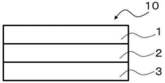
- FIG. 1 is a typical sectional view showing an example of an embodiment of a decoration sheet of the present invention.
- FIG. 2 is a scanning electron micrograph of a cross section of an example of a cholesteric liquid crystal layer shown as a reference.
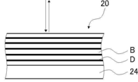
- FIG. 3 is a schematic cross-sectional view for explaining the action of reflection of the cholesteric liquid crystal layer.
- FIG. 4 is a schematic cross-sectional view for explaining the action of reflection of the cholesteric liquid crystal layer.
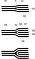
- Drawing 5 is a typical sectional view showing an example of an embodiment of a decoration sheet of the present invention.
- FIG. 6 is a scanning electron micrograph of a cross section of an example of a cholesteric liquid crystal layer shown as a reference.
- FIG. 7 shows the mask patterns used in Examples 29 and 30.
- FIG. 8 shows the mask pattern used in Examples 29 and 30.
- a numerical range expressed using “to” means a range including numerical values described before and after “to” as a lower limit value and an upper limit value.
- parallel and orthogonal do not mean parallel or orthogonal in a strict sense, but mean a range of ⁇ 5 ° from parallel or orthogonal.
- Re ( ⁇ ) and Rth ( ⁇ ) represent in-plane retardation and retardation in the thickness direction at the wavelength ⁇ , respectively. Unless otherwise specified, the wavelength ⁇ is 550 nm.
- Re ( ⁇ ) and Rth ( ⁇ ) are values measured at a wavelength ⁇ in AxoScan (manufactured by Axometrics).
- ⁇ the average refractive index
- d film thickness
- Re ( ⁇ ) R0 ( ⁇ )
- Rth ( ⁇ ) ((nx + ny) / 2 ⁇ nz) ⁇ d Is calculated.
- R0 ( ⁇ ) is displayed as a numerical value calculated by AxoScan, and means Re ( ⁇ ).
- liquid crystal composition and the liquid crystal compound include a concept that no longer exhibits liquid crystallinity due to curing or the like.
- Drawing 1 is a typical sectional view showing an example of an embodiment of a decoration sheet of the present invention.
- the decorative sheet 10 of the present invention has a cholesteric liquid crystal layer 1 having wavelength selective reflectivity. Further, the undercoat layer 2 and the support 3 may be provided.
- the decorative sheet 10 of the present invention has a non-viewing side surface opposite to the viewing side surface and the viewing side surface.
- the decorative sheet 10 of the present invention may have a pattern shape in which a portion satisfying the requirements of the present invention and a portion not satisfied are mixed in the plane of the sheet.
- a decorative part indicating glitter
- a mask is applied and a cholesteric liquid crystal layer is applied (the mask portion is not applied with a liquid crystal layer), and a uniformly applied cholesteric liquid crystal layer is partially isotropic with respect to temperature or the like
- a uniformly applied cholesteric liquid crystal layer is partially isotropic with respect to temperature or the like Examples include, but are not limited to, forming a layer and drawing a cholesteric liquid crystal layer by inkjet.
- the decorative sheet 10 of the present invention may have a plurality of reflection regions having different peak wavelengths of characteristic reflection in the surface of the sheet, and a plurality of cholesteric liquid crystal layers 1 having different peak wavelengths of characteristic reflection. You may have the area
- the decorative sheet 10 of the present invention can have various shapes, and there are no particular limitations such as various figures and characters.
- the shape of each region is not particularly limited, and various shapes such as a stripe shape, a dot shape, and a mosaic shape can be used.
- the size of each reflective area is not particularly limited. You may have a fine structure which can observe the reflected light of each reflective area
- the decorative sheet 10 of the present invention may further include any one of a light transmission region, a light reflection layer, a light absorption layer, an ultraviolet absorption layer, and an antireflection layer, or a combination thereof.
- the decorative sheet 10 of the present invention is not limited to a flat sheet, and may be processed into a three-dimensional shape. Stretching and shrinking may be used for processing into a three-dimensional shape.
- the decorative sheet 10 of the present invention can also be a highly applicable decorative material when used in combination with a ⁇ / 4 retardation plate.
- a ⁇ / 4 retardation plate For example, when the surface of the liquid crystal display element (display) is decorated with the decorative sheet of the present invention via a ⁇ / 4 retardation plate, the color of the decorative sheet is visible only when the display is turned off or when the display is black. In the case of display, decoration with a unique design that is transparent and has no presence is possible.
- the liquid crystal display device of the present invention provided with the composite film having the decorative sheet 10 of the present invention and the ⁇ / 4 retardation plate on the surface (image display surface), when the display device is turned off or in black display Only the color of the decorative sheet 10 can be seen, and in the case of white display, a liquid crystal display device having a unique design with transparency and no presence can be realized.
- the composite film having the decorative sheet 10 and the ⁇ / 4 retardation plate of the present invention can be used as a reflection plate for a reflective liquid crystal display element, a transflective liquid crystal display element, or the like.
- the decorative sheet 10 of the present invention is visually recognized as a decorative material when the viewing side is bright through a film like a half mirror and is not visible through the back side, and is visible as a transparent film when the back side is bright. It is possible to have a unique design.
- the ⁇ / 4 retardation plate and the decorative sheet 10 of the present invention are combined, and the decorative sheet 10 side is used for decorating the dashboard in front of the windshield of the car, so that the windshield is obtained.
- the composite film having the decorative sheet 10 and the ⁇ / 4 retardation plate of the present invention is not limited to this application, and is used in various ways for the purpose of preventing an article applied to the decoration from being reflected on the reflector. Is possible.
- the in-plane retardation Re of the ⁇ / 4 retardation plate is not particularly limited, but the ⁇ / 4 retardation plate has an in-plane retardation Re (550) of a wavelength of 550 nm from 115 nm to It is preferably 165 nm, more preferably 120 nm to 150 nm, and even more preferably 125 nm to 145 nm.
- the retardation Rth in the thickness direction of the ⁇ / 4 retardation plate is not particularly limited, but the retardation Rth (550) in the thickness direction of the wavelength 550 nm of the ⁇ / 4 retardation plate is ⁇ 200 nm. It is preferably from ⁇ 200 nm, more preferably from ⁇ 100 nm to 100 nm, and even more preferably from ⁇ 50 nm to 50 nm.
- the decorative sheet 10 of the present invention satisfies the following formula (1).
- R [ ⁇ 45, 20] ( ⁇ ) is the polar angle 20 at an azimuth angle that is 180 ° shifted from the azimuth angle of the incident light with respect to the incident light having a polar angle of ⁇ 45 ° to the decorative sheet 10.
- ⁇ 1 represents the peak wavelength at a wavelength of 380 nm to 780 nm of the characteristic reflectance measured as light enters from the viewing side surface of the decorative sheet 10;
- filling Formula (1) when it observes from the direction remove
- the decorative sheet 10 of the present invention preferably satisfies the following formula (1-1), more preferably satisfies the following formula (1-2), and particularly preferably satisfies the following formula (1-3).
- this formula it is possible to further improve the glitter when observed from a direction deviating from the regular reflection of the illumination light.
- “brightness when observed from a direction deviating from regular reflection of illumination light” is also simply referred to as “brightness”.
- R [ ⁇ 45, 20] ( ⁇ 1) / R [ ⁇ 45, 20] ( ⁇ 2) there is no particular upper limit for R [ ⁇ 45, 20] ( ⁇ 1) / R [ ⁇ 45, 20] ( ⁇ 2), but it is preferable that the following formula (1-3) is satisfied.
- the decorating sheet 10 of this invention satisfy
- R [ ⁇ 45,15] ( ⁇ ) is a polar angle 15 at an azimuth angle that is 180 ° shifted from the azimuth angle of the incident light with respect to incident light having a polar angle of ⁇ 45 ° to the decorative sheet 10. It is the reflectance at a wavelength ⁇ measured at a light receiving angle of °. Satisfying the formula (2) is preferable in that a rapid change in the reflection intensity due to the reflection angle is suppressed and the texture is excellent.
- the decorative sheet 10 of the present invention more preferably satisfies the following formula (2-1).
- the decorating sheet 10 of this invention has the area
- R max [0,15] ( ⁇ ) and R max [0,15] ( ⁇ ) are a wavelength ⁇ and a polar angle of 15 ° with respect to incident light with a polar angle of 0 ° to the decorative sheet 10.
- Having the region A satisfying the expression (3) is preferable in that the reflection intensity varies depending on the viewing azimuth and a unique design can be obtained.
- the decorative sheet 10 of the present invention has a region A1 that satisfies the following formula (3-1).
- the decorating sheet 10 of this invention further has the area
- R max [0,15] ( ⁇ ) and R max [0,15] ( ⁇ ) are a wavelength ⁇ and a polar angle of 15 ° with respect to incident light with a polar angle of 0 ° to the decorative sheet 10.
- Having the region A satisfying the formula (4) is preferable in that a unique design property is increased by mixing regions having different reflection intensities depending on the viewing azimuth and equivalent regions.
- a plurality of areas A and B may exist in the surface of the decorative sheet 10. Moreover, there is no limitation in particular also about a shape. They may be randomly arranged or regularly arranged.
- the reflectance means an incident angle (polar angle, azimuth angle), a light receiving angle (polar angle, azimuth angle), and a measurement wavelength region so that light enters from the viewing side surface of the decorative sheet 10. Is a value measured using a three-dimensional variable angle spectral colorimetry system (Murakami Color Research Laboratory Co., Ltd., GCMS-3B). If the reflectance is out of the wavelength range measurable by the apparatus, an absolute reflectance measurement unit (JASCO Corporation) can be used as an alternative to a spectrophotometer (manufactured by JASCO Corporation, V-770). Measurement may be performed using a product equipped with ARMN-920).
- JASCO Corporation absolute reflectance measurement unit
- the characteristic reflectance means that a spectrophotometer (manufactured by JASCO Corp., V-550) is fitted with a large integrating sphere device (JASCO ( It is a value measured using a product equipped with ILV-471) manufactured by Co., Ltd. so as to include specularly reflected light without using an optical trap.
- JASCO a large integrating sphere device
- the peak wavelength of the characteristic reflectance when the reflection spectrum of the reflection region is measured by the above method, a waveform of the characteristic reflectance having a mountain shape (convex upward) with the wavelength as the horizontal axis is obtained.
- the maximum value of the integrated reflectance excluding the regular reflection component in the wavelength range of 380 nm to 780 nm is preferably 10% or more. It is more preferably 30% or more, and further preferably 40% or more. By setting it as the said range, glitter can be improved more.
- the integrated reflectance excluding the specular reflection component is a large integrating sphere device in a spectrophotometer (manufactured by JASCO Corporation, V-550) so that light enters from the viewing side surface of the decorative sheet. This is a value measured by using an optical trap attached with (ILV-471 manufactured by JASCO Corporation) so as not to include specularly reflected light.
- the ratio of the internal haze value (Hi) to the total haze value (Ht) is preferably 40% or more, and more preferably 70% or more. By setting it as the said range, glitter can be improved more.
- the total haze value (Ht) and the internal haze value (Hi) are values measured under the following conditions based on JIS K-7136 (2000).
- Device name Haze meter NDH2000 (manufactured by Nippon Denshoku Industries Co., Ltd.)
- Sample size 50 mm x 50 mm
- Measurement environment 55 ° C, relative humidity 55%
- the support 3 supports the cholesteric liquid crystal layer.
- the support 3 used in the present invention may be a single layer or a multilayer.
- Examples of the support 3 in the case of a single layer include a support made of glass, triacetyl cellulose (TAC), polyethylene terephthalate (PET), polycarbonate, polyvinyl chloride, acrylic, polyolefin, cycloolefin polymer, and the like. However, it is not particularly limited to these.
- Examples of the support in the case of a multilayer include those in which any one of the above-described single-layer supports is included as a substrate, and another layer is provided on the surface of the substrate.
- a ⁇ / 4 retardation plate may be used as the support 3.
- a (meth) acrylic polymer resin such as a resin obtained by curing a polyfunctional (meth) acrylic monomer such as pentaerythritol triacrylate or pentaerythritol tetraacrylate, a polyvinyl alcohol resin
- a plurality of undercoat layers 2 may be laminated. Especially, it is preferable that an undercoat layer contains (meth) acrylic polymer resin or polyvinyl alcohol resin at the point which the effect of this invention is excellent.
- the (meth) acrylic polymer resin is a concept including an acrylic polymer resin and a methacrylic polymer resin.
- the undercoat layer containing a (meth) acrylic polymer resin is preferably a layer formed by curing a composition containing a polyfunctional (meth) acrylic monomer.
- the polyfunctional (meth) acrylic monomer may be a monomer having two or more (meth) acryloyl groups, and the number of (meth) acryloyl groups is preferably 2 to 8, and more preferably 2 to 6.
- the (meth) acryloyl group is a concept including an acryloyl group and a methacryloyl group.
- the molecular weight of the polyfunctional (meth) acrylic monomer is not particularly limited, but is preferably 1000 or less, and more preferably 500 or less. The lower limit is not particularly limited, but is often 100 or more.
- the composition containing the polyfunctional (meth) acrylic monomer may contain a polymerization initiator.
- a method for forming an undercoat layer containing a (meth) acrylic polymer resin using the above composition for example, a coating film is formed by applying a composition containing a polyfunctional (meth) acrylic monomer on a predetermined support. Furthermore, the method of giving a hardening process (for example, photocuring process and thermosetting process) to a coating film is mentioned.
- a modified polyvinyl alcohol resin into which a predetermined functional group (for example, a polymerizable group) is introduced may be used.
- a method for forming an undercoat layer containing a polyvinyl alcohol resin for example, a coating film is formed by applying a composition containing a polyvinyl alcohol resin on a predetermined support, and if necessary, the coating film is dried. A method is mentioned.
- the cholesteric liquid crystal layer 1 used in the present invention is a layer formed by fixing a cholesteric liquid crystal phase and has wavelength selective reflectivity.
- the light in which the cholesteric liquid crystal layer 1 exhibits wavelength selective reflectivity is not particularly limited and may be, for example, infrared (infrared light), visible light, ultraviolet light (ultraviolet light), or the like.
- the cholesteric liquid crystal layer 1 used in the present invention is preferably a liquid crystal compound fixed in a cholesteric alignment state.
- the cholesteric alignment state may include both an alignment state that reflects right circularly polarized light and an alignment state that reflects left circularly polarized light.
- the liquid crystalline compound used in the present invention is not particularly limited, and various known compounds can be used.
- the cholesteric liquid crystal layer 1 used in the present invention has a stripe pattern of a bright part and a dark part when a cross section is observed using a scanning electron microscope (SEM). It is preferable.
- the SEM photograph of FIG. 2 shows the cross section of an example of a cholesteric liquid crystal layer to the last, and does not show embodiment of the cholesteric liquid crystal layer in the decorating sheet
- the striped pattern preferably has a corrugated structure, and the average value of the peak-to-peak distance of the corrugated structure is preferably 0.5 ⁇ m to 50 ⁇ m.
- the thickness is more preferably 1.5 ⁇ m to 10 ⁇ m, and further preferably 2.5 ⁇ m to 5.0 ⁇ m.
- the striped pattern of the bright part and the dark part is preferable in terms of having a wavy structure and making the average value of the peak-to-peak distance of the wavy structure within the above range, so that the glitter can be further improved.
- FIG. 3 conceptually shows a cross section of a general cholesteric liquid crystal layer.
- a stripe pattern of a bright part B and a dark part D is usually observed in the cross section of a general cholesteric liquid crystal layer 20 . That is, in the cross section of the cholesteric liquid crystal layer 20, a layered structure in which bright portions B and dark portions D are alternately stacked is observed.
- the stripe pattern (layered structure) of the bright part B (continuous line formed by the bright part B) and the dark part D (continuous line formed by the bright part B) is, as shown in FIG.
- the cholesteric liquid crystal layer 20 is formed so as to be parallel to the formation surface.
- the cholesteric liquid crystal layer 20 exhibits specular reflectivity. That is, when light is incident from the normal direction of the cholesteric liquid crystal layer 20, the light is reflected in the normal direction, but the light is hardly reflected in the oblique direction (see the arrow in FIG. 3).
- the bright part B and the dark part D have a wavy structure (uneven structure, wave structure) as in the cholesteric liquid crystal layer 26 conceptually shown in cross section in FIG. 4, a cholesteric liquid crystal phase is formed. Since there is a region where the spiral axis of the liquid crystal compound to be inclined, when light is incident from the normal direction of the cholesteric liquid crystal layer 26, a part of the incident light is reflected in an oblique direction (see the arrow in FIG. 4). ). That is, the bright portion B and the dark portion D have a waved structure, so that the cholesteric liquid crystal layer 26 having appropriate diffuse reflectance is obtained.
- the wavy structure includes at least one region M in which the absolute value of the inclination angle with respect to the plane of the cholesteric liquid crystal layer 1 is 5 ° or more in the continuous line of the bright or dark portion of the striped pattern. Means that two peaks or valleys with an inclination angle of 0 ° located at the closest position are specified.
- a peak or valley with an inclination angle of 0 ° includes a convex shape and a concave shape.
- the peak-to-peak distance of the wavy structure is the distance between the cholesteric liquid crystal layer 1 in the plane direction of two peaks or valleys at an inclination angle of 0 °, which are closest to each other with the region M interposed therebetween. It is a value obtained by arithmetically averaging the length of the layer in the longitudinal direction of the cross section of 100 ⁇ m and the total film thickness.
- each continuous line when each continuous line is in contact with either interface of the film and is broken, both ends of the broken point are not regarded as peaks or valleys.
- each continuous line has a bent structure as shown in FIG. 2, the continuous line is regarded as being interrupted there, and both ends thereof are not regarded as peaks or valleys.
- the cholesteric liquid crystal layer 1 used in the present invention has a decorative sheet when the angle formed by the fine line segment on the continuous line of the bright part or dark part of the striped pattern and the normal direction of the decorative sheet is an inclination angle. It is preferable that the following formula (5) and the following formula (6) are satisfied, where ⁇ and ⁇ are the largest from among the standard deviations of the respective inclination angles within 1 ⁇ m from the two surfaces. ⁇ / ⁇ ⁇ 1.2 Formula (5) ⁇ ⁇ 2 ° Formula (6) By satisfy
- the cholesteric liquid crystal layer 1 used in the present invention preferably satisfies the following formula (5-1), and more preferably satisfies the following formula (5-2). It is more preferable to satisfy the following formula (6-1). ⁇ / ⁇ ⁇ 1.9 Formula (5-1) ⁇ / ⁇ ⁇ 2.2 Formula (5-2) ⁇ ⁇ 10 ° Formula (6-1)
- the cholesteric liquid crystal layer 1 used in the present invention preferably has a stripe pattern of a bright part and a dark part when the cross section is observed with an SEM.
- at least one of bright portions (continuous lines of bright portions) and dark portions (continuous lines of dark portions) forming a stripe pattern is branched,
- the branched bright part and dark part there is a bright part or dark part having an end toward the branch part between two bright parts or dark parts of the three bright parts or dark parts extending from the branch part,
- the number of the structures A and B included per 100 ⁇ m 2 of the cross section of the cholesteric liquid crystal layer 1 satisfy one of the following conditions I and II.
- Condition I is that the structure B is not included and the structure A is included in the range of 0.1 to less than 50.
- Condition II is that the structure B includes 0.1 or more and less than 10 structures B.
- the dark part is branched, and three dark parts (continuous lines of dark part) D1, dark part D2, and dark part D3 extend from branch part X1, Between the dark part D2 and the dark part D3, a bright part (continuous line of bright part) B1 having an end toward the branch part X1 exists. That is, the two dark parts having the bright part B1 having an end toward the branch part X1 are the dark part D2 and the dark part D3. In other words, the two dark parts, the dark part D2 and the dark part D3, sandwich the bright part B1 having an end toward the branch part X1.
- only the bright part B1 that is, the bright part B1 having an end toward the branch part X1
- the structure by this branch part X1 becomes the structure A.
- the dark part is branched, and three dark parts D4, dark parts D5, and dark parts D6 extend from the branched part X2, and between the two dark parts D5 and dark part D6, There is a dark portion D7 having an end toward the branch portion X2. That is, the two dark portions sandwiching (having between) the dark portion D7 having an end toward the branch portion X2 are the dark portion D5 and the dark portion D6.
- the dark part D5 and the dark part D6 there are three bright parts B and dark parts D of the dark part D7, the bright part B2, and the bright part B3. Therefore, the structure by this branch part X2 becomes the structure B.
- the dark part is branched and has an end portion toward the branch part between two dark parts of the three dark parts extending from the branch part.
- the branch part There is a bright part, and there are five bright parts and a dark part of three bright parts and two dark parts between two dark parts sandwiching the bright part. Therefore, the structure by this branch part is the structure B.
- the bright part and the dark part that are folded back so as to sandwich the bright part or the dark part having an end toward the branch part are counted in two. Further, as described above, in the cholesteric liquid crystal layer, continuous lines of bright portions and dark portions are alternately formed to form a striped pattern. Therefore, the number of bright parts and dark parts between two bright parts or dark parts with a bright part or dark part having an end toward the branch part in between is an odd number.
- FIG. 6 shows a cross-section of an example of a cholesteric liquid crystal layer only for the purpose of explaining the structure A and the structure B, and an embodiment of the cholesteric liquid crystal layer in the decorative sheet of the present invention. It does not indicate.
- the portion indicated by a circle A has a bright portion branched, and a dark portion having an end toward the branched portion of the branched bright portion is between two of the three branched bright portions.
- a dark part having an end toward the branch part is sandwiched (having a dark part in between), and there is only one dark part between two bright parts. Therefore, the structure by this branch part is the structure A.
- a dark portion is branched in a portion indicated by a circle B, and a dark portion having an end portion toward the branch portion of the branched dark portion exists between two of the three branched bright portions. .
- the structure by this branch part is the structure B.
- the part indicated by a circle C has a dark part branched, and a dark part having an end toward the branched part of the branched dark part exists between two of the three branched dark parts. To do. Between the two dark parts sandwiching the dark part having an end toward the branch part of the dark part, there are seven bright parts and a dark part of three dark parts and four bright parts. Therefore, the structure by this branch part is the structure B.
- the cholesteric liquid crystal layer 1 used in the decorative sheet of the present invention preferably has the number of structures A and B included in a cross section of 100 ⁇ m 2 observed by SEM, “the structure B is not included and the structure A is not included.
- One of the conditions I of “including 0.1 or more and less than 50” and the condition II of “including 0.1 or more and less than 10 structures B” is satisfied.
- the structure A may or may not be included per 100 ⁇ m 2 of the cross section of the cholesteric liquid crystal layer 1.
- the number of the structures A included per 100 ⁇ m 2 is preferably 40 or less. More preferably, the number is less than or equal to.
- the branch of the bright part B and the dark part D in the cholesteric liquid crystal layer 1 is a part where the alignment of the liquid crystalline compound forming the cholesteric liquid crystal layer 1 is disturbed.
- the cholesteric liquid crystal layer 1 exhibits diffuse reflectivity. Therefore, the cholesteric liquid crystal layer 1 has higher diffuse reflectivity as the number of bright part B and dark part D branches increases.
- the structure B has a stronger disorder of the alignment of the liquid crystal compound, and the diffuse reflectance is also stronger in the structure B than in the structure A.
- the cholesteric liquid crystal layer 1 satisfies any one of the conditions I and II that define the number of structures A and B per unit area, so that the cholesteric liquid crystal layer 1 has an appropriate diffuse reflection. It can enhance the brightness and enhance the brightness.
- the number of the structures A and B included per 100 ⁇ m 2 of the cross section of the cholesteric liquid crystal layer 1 is a region having an area of 100 ⁇ m 2 that does not overlap with each other in the cross section of the cholesteric liquid crystal layer 1 observed by SEM. , Arbitrarily select 10 locations, count the number of structures A and B in each region, and include the average number of structures A and structures B in 10 regions per 100 ⁇ m 2 cross section of the cholesteric liquid crystal layer And the number of structures A and B.
- the surface roughness of the cholesteric liquid crystal layer 1 used in the present invention is preferably 100 nm or less. By setting the surface roughness of the cholesteric liquid crystal layer to 100 nm or less, it is preferable from the viewpoint that the surface has no whiteness and is excellent in design.
- the surface roughness is a surface roughness (arithmetic average roughness Ra) measured using a non-contact three-dimensional surface shape measuring instrument (VertScan manufactured by Ryoka System Co., Ltd.).
- the cholesteric liquid crystal layer 1 used in the present invention is formed by, for example, forming an undercoat layer 2 made of a hydrophilic resin such as polyvinyl alcohol on a support 3, applying a liquid crystalline composition thereon, and fixing in a cholesteric alignment state. Can be obtained. If the support 3 is subjected to corona treatment or the like to make the surface of the support 3 hydrophilic, the undercoat layer is not necessarily required.
- the support 3 and the undercoat layer 2 are not given an orientation regulating force or are given a weak orientation regulating force.
- the rubbing process is not performed or a weak rubbing process is performed.
- the support 3 or the undercoat layer 2 is preferably smooth, but the support 3 and / or the undercoat layer 2 may have a concavo-convex structure in advance in order to obtain the above-described corrugated structure.
- the concavo-convex structure may be regular or irregular (random).
- the cholesteric alignment spiral axis in the cholesteric liquid crystal layer 1 may be inclined.
- the average absolute value of the inclination angle of the helical axis is preferably 4 ° to 15 °.
- the cholesteric liquid crystal layer 1 in which the helical axis is inclined can be formed by using, for example, spin coating.
- the temperature is adjusted to obtain a cholesteric alignment state, and the temperature lowering rate at that time is preferably 0.4 ° C. to 60 ° C. per second, particularly 2 ° C. to 12 ° C. per second. preferable.
- the temperature lowering rate at that time is preferably 0.4 ° C. to 60 ° C. per second, particularly 2 ° C. to 12 ° C. per second. preferable.
- the cholesteric liquid crystal layer 1 used in the present invention may have a surfactant.
- a surfactant By using a surfactant, a cholesteric liquid crystal layer satisfying the above-described formulas (5) and (6) can be effectively obtained.
- a surfactant having a property of aligning a liquid crystalline compound in the vicinity of the air interface of the cholesteric liquid crystal layer 1 in parallel with the cholesteric liquid crystal layer surface.
- the surfactant may be either a fluorine-based surfactant or a silicone-based surfactant, but is preferably a fluorine-based surfactant.
- the surfactant preferably has a mesogen moiety in the molecule in order to align the liquid crystalline compound in the vicinity of the air interface of the cholesteric liquid crystal layer 1 in parallel with the surface of the cholesteric liquid crystal layer. It is preferable to have a group having a surface-active function at the terminal, preferably at both terminals.
- the cholesteric liquid crystal layer 1 used in the present invention preferably contains a large amount of a surfactant on the air interface side surface.
- the surface uneven distribution of the surface activity can be confirmed, for example, by measuring the existence ratio of fluorine atoms on both surfaces of the cholesteric liquid crystal layer 1.
- the cholesteric liquid crystal layer 1 used in the present invention may contain a chiral agent.
- Various known agents can be used as the chiral agent.
- Example 1 ⁇ Preparation of transparent support 1> The following composition was put into a mixing tank and stirred while heating to dissolve each component to prepare a cellulose acetate solution.
- Cellulose acetate solution composition Cellulose acetate having an acetylation degree of 60.7 to 61.1% 100 parts by weight Triphenyl phosphate (plasticizer) 7.8 parts by weight Biphenyl diphenyl phosphate (plasticizer) 3.9 parts by weight Methylene chloride (first solvent) 336 parts by weight Methanol (second solvent) 29 parts 1-butanol (third solvent) 11 parts
- a dope was prepared by mixing 474 parts by mass of the cellulose acetate solution with 25 parts by mass of the retardation increasing agent solution and stirring sufficiently.
- the addition amount of the retardation increasing agent was 6.0 parts by mass with respect to 100 parts by mass of cellulose acetate.
- the obtained dope was cast using a band stretching machine. After the film surface temperature on the band reaches 40 ° C., the film is dried with warm air of 70 ° C. for 1 minute, and the film is dried from the band with 140 ° C. of drying air for 10 minutes. A triacetylcellulose film was prepared. This film is referred to as a transparent support 01.
- undercoat layer coating solution having the following composition was applied to the surface of the transparent support 01 with a # 16 wire bar coater. Thereafter, the film was dried at 60 ° C. for 60 seconds and further at 90 ° C. for 150 seconds. A transparent support 01 with an undercoat layer was produced.
- Methyl ethyl ketone 145.0 parts by weight Mixture of the following rod-like liquid crystalline compounds 100.0 parts by weight IRGACURE 907 (manufactured by Ciba Geigy) 3.0 parts by weight Kayacure DETX (manufactured by Nippon Kayaku Co., Ltd.) 1.0 part by weight Chiral Agent A 5.78 parts by mass Surfactant F1 0.08 parts by mass of the following structure
- Rod-like liquid crystalline compound The numerical value is mass%.
- R is a group bonded by an oxygen atom.
- the cholesteric liquid crystal layer coating solution Gm1 is a material for forming a cholesteric liquid crystal layer that reflects light having a central wavelength of 550 nm.
- the cholesteric liquid crystal layer coating liquid Gm1 is a material for forming a reflective layer that reflects right circularly polarized light. That is, the cholesteric liquid crystal layer coating liquid Gm1 is a material for reflecting right-polarized green.
- the cholesteric liquid crystal layer coating solution Gm1 prepared above is applied to the surface of the transparent support 01 with an undercoat layer with a spin coater at a rotation speed of 1500 rpm for 10 seconds, dried at 95 ° C. for 60 seconds, and then cooled to 25 ° C.
- the decorative sheet 01 was manufactured by lowering the temperature at ⁇ 7 ° C./s until irradiation of 500 mJ / cm 2 with an ultraviolet irradiation device at 25 ° C.
- Example 2 In Example 1, decorative sheets 02 to 06 of Examples 2 to 6 were produced in the same manner except that the amount of the surfactant F1 in the coating liquid Gm1 for the cholesteric liquid crystal reflective layer was changed as shown in Table 1. did.
- Example 7 In Example 1, the produced transparent support 01 with an undercoat layer was rubbed by rotating it with a rubbing roll in a direction parallel to the conveying direction at a clearance of 2.0 mm and 1000 rpm, and this is shown in Table 1.
- the decorative sheets 07 to 10 of Examples 7 to 10 were produced in the same manner except that the above process was repeated.
- the setting of the rubbing clearance of 2.0 mm is a weak condition for imparting the alignment regulating force, and was performed in order to gently control the alignment state of the liquid crystal in the vicinity of the undercoat layer.
- Example 11 the prepared cholesteric liquid crystal reflective layer coating liquid Gm1 was applied to the surface of the prepared transparent support with an undercoat layer 01 using a spin coater at a rotational speed of 1500 rpm for 10 seconds and at 95 ° C. After drying for 60 seconds, the temperature was lowered under the conditions shown in Table 1 until reaching 25 ° C., and in the same manner as in Examples 11 to 11, except that 500 mJ / cm 2 of ultraviolet rays was irradiated at 25 ° C. with an ultraviolet irradiation device. 22 decorative sheets 11 to 22 were prepared.
- Example 2 the prepared cholesteric liquid crystal reflective layer coating liquid Gm1 was applied to the surface of the prepared transparent support 01 with an undercoat layer with a spin coater at a rotational speed shown in Table 1 for 10 seconds. After drying at 95 ° C. for 60 seconds, the temperature was lowered to ⁇ 7 ° C./second until reaching 25 ° C., and the procedure was carried out in the same manner except that 500 mJ / cm 2 of ultraviolet rays were irradiated by an ultraviolet irradiation device at 25 ° C. Decorative sheets 23 to 26 of Examples 23 to 26 were produced.
- Example 27 Using the transparent support 01 with an undercoat layer of Example 1, it was produced as follows. ⁇ Preparation of undercoat layer 02> An undercoat layer coating solution 02 having the following composition was applied to the surface of the transparent support 01 with an undercoat layer with a # 3.6 wire bar coater. Then, it dried at 95 degreeC for 60 second, and irradiated the ultraviolet ray of 500 mJ / cm ⁇ 2 > with the ultraviolet irradiation device at 25 degreeC, and produced the transparent support body 02 with an undercoat layer.
- KAYARAD PET30 (manufactured by Nippon Kayaku Co., Ltd.) 100 parts by mass IRGACURE 907 (manufactured by Ciba Geigy) 3.0 parts by mass Kaya Cure DETX (manufactured by Nippon Kayaku Co., Ltd.) 1.0 part by mass Methyl ethyl ketone 120 parts by mass KAYARAD PET30 Is a mixture of pentaerythritol triacrylate and pentaerythritol tetraacrylate (PETA).
- a cholesteric liquid crystal layer coating solution Gm1 prepared in the same manner as in Example 1 was applied to the surface of the transparent support 02 with an undercoat layer using a # 8.0 wire bar coater. Thereafter, after drying at 95 ° C. for 60 seconds, the temperature was lowered to ⁇ 7 ° C./s until reaching 25 ° C., and irradiation of 500 mJ / cm 2 of ultraviolet rays was performed at 25 ° C. with an ultraviolet irradiation device. A decorative sheet 27 was produced.
- Example 1 the produced transparent support 01 with an undercoat layer was rubbed by rotating it with a rubbing roll in a direction parallel to the conveying direction at a clearance of 1.6 mm and 1000 rpm, and applied to a cholesteric liquid crystal reflective layer.
- Liquid Gm1 was applied with a spin coater at a rotation speed of 1500 rpm for 10 seconds, dried at 95 ° C. for 60 seconds, and then irradiated with ultraviolet light of 500 mJ / cm 2 by an ultraviolet irradiation device to decorate Comparative Example 1.
- a sheet 101 was produced.
- the setting of the rubbing clearance of 1.6 mm is a strong condition for imparting the alignment regulating force, and was performed in order to strongly control the alignment state of the liquid crystal in the vicinity of the undercoat layer.
- Comparative Example 2 A decorative sheet 102 of Comparative Example 2 was produced in the same manner as in Example 1 except that the surfactant F1 of the coating liquid Gm1 for cholesteric liquid crystal reflective layer was not added.
- Example 3 In Example 1, the surfactant F1 of the coating liquid Gm1 for cholesteric liquid crystal reflective layer was not added, but instead of 0.4 parts by mass of the surfactant F2 having the following structure, the same procedure as in Comparative Example 3 was performed. A decorative sheet 103 was produced.
- a decorative sheet 104 of Comparative Example 4 was produced in the same manner as [0092] to [0102] in the examples of Japanese Patent No. 4170834.
- AC-X used as the undercoat layer is a polyester-based easy adhesive.
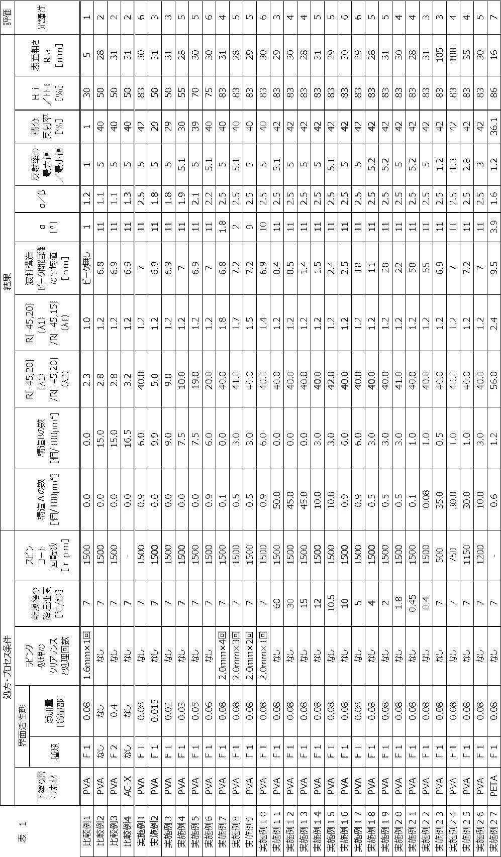
- Table 1 shows the results of measurement and evaluation performed on the decorative sheets prepared in Examples and Comparative Examples.
- ⁇ Number of structures A and B> In the cross-sectional SEM photograph of the formed cholesteric liquid crystal layer, arbitrarily select 10 regions of 100 ⁇ m 2 , count the number of structures A and B in each region, and calculate the average value of 10 locations for each decorative sheet. The number of structures A and B per 100 ⁇ m 2 cross section of the cholesteric liquid crystal layer was used.
- the peak wavelength of the characteristic reflectance was obtained in accordance with the above-described characteristic reflectance measurement method. In any of the decorative sheets of Examples and Comparative Examples, the peak wavelength of the characteristic reflectance was in the vicinity of 550 nm.
- the range of 5cm x 5cm of each decorative sheet is the wavelength ⁇ , polar angle 15 °, azimuth angle 0 ° ⁇ 360 ° with respect to the incident light of polar angle -45 ° to the decorative sheet every 500 ⁇ m.
- R max [0,15] ( ⁇ 1) and R min [0,15] ( ⁇ 1) at the respective light receiving angles are obtained, and R max [0,15] ( ⁇ 1) / R min [0,15] are obtained.
- the value at which ( ⁇ 1) is maximum is shown in Table 1 as the maximum value / minimum value of reflectance.
- Example 28 In Example 1, except that the rotation time when applying the cholesteric liquid crystal layer coating solution Gm1 prepared above on the surface of the transparent support 01 with the undercoat layer prepared with a spin coater was set to 2 seconds. In the same manner as in Example 1, a decorative sheet 28 was produced.
- R [ ⁇ 45, 20] ( ⁇ 1) and R [ ⁇ 45, 20] ( ⁇ 2) are measured in the same manner as described above in accordance with the reflectance measurement method described above.
- R [ ⁇ 45,20] ( ⁇ 1) / R [ ⁇ 45,20] ( ⁇ 2) at the center of the decorative sheet and R [ ⁇ 45,20] ( ⁇ 1) / R at the periphery [ ⁇ 45, 20] ( ⁇ 2) was calculated.
- R [ ⁇ 45, 20] ( ⁇ 1) / R [ ⁇ 45, 20] ( ⁇ 2) 40.0 at the center of the decorative sheet
- R [ ⁇ 45, 20] ( ⁇ 2) 40.0.
- the maximum value / minimum value of the reflectance at and the maximum value / minimum value of the reflectance at the periphery were calculated.
- the maximum value / minimum value of the reflectance was 1.08 in the center portion of the decorative sheet, and the maximum value / minimum value was 1.3 in the peripheral portion.
- the decorative sheet 28 has sharpness in the surface, and a texture with high designability can be realized as a decoration application.
- Example 29 (Preparation of coating liquid Gm2 for cholesteric liquid crystal reflective layer) After the following composition was prepared, it was filtered through a polypropylene filter having a pore size of 0.2 ⁇ m and used as a coating liquid Gm2 for a cholesteric liquid crystal reflective layer.
- LC-1-1 was synthesized based on the method described in JP-A No. 2004-12382.
- LC-1-1 is a liquid crystal compound having two reactive groups, one of the two reactive groups is an acrylic group which is a radical reactive group, and the other is an oxetane group which is a cationic reactive group. It is.
- LC-1-2 is Tetrahedron Lett. It was synthesized according to the method described in Journal, Vol. 43, page 6793 (202).
- ⁇ Cholesteric liquid crystal reflective layer coating solution Gm2 (parts by mass) ⁇ Rod-shaped liquid crystal (LC-1-1) 19.57 Horizontal alignment agent (LC-1-2) 0.01 Cationic monomer (OXT-121, manufactured by Toagosei Co., Ltd.) 0.98 Cationic initiator (Cureure UVI 6974, manufactured by Dow Chemical) 0.4 Polymerization control agent (IRGANOX1076, manufactured by BASF) 0.02 Chiral agent A 1.13 Methyl ethyl ketone 80.0 ⁇
- Example 1 (Formation of patterned cholesteric liquid crystal reflective layer)
- the prepared cholesteric liquid crystal reflective layer coating liquid Gm2 was applied to the surface of the transparent support 01 with the undercoat layer by a spin coater at a rotation speed of 1500 rpm and a rotation time of 10 seconds, and at 95 ° C. Aged for 60 seconds, and then immediately irradiated with 500 mJ / cm 2 of ultraviolet light using an air-cooled metal halide lamp (produced by Eye Graphics Co., Ltd.) at an air temperature of 70 ° C. to fix the orientation state. By doing so, the pattern preparation material was formed.
- the protective layer coating solution AD-1 prepared above is applied onto the pattern preparation material thus obtained, dried at 80 ° C.
- R [ ⁇ 45,20] ( ⁇ 1) / R [ ⁇ 45,20] ( ⁇ 2) was calculated.
- R [ ⁇ 45,20] ( ⁇ 1) / R [ ⁇ 45,20] ( ⁇ 2) 40.0.
- the decorative sheet 29 has sharpness in the surface, and a texture with high designability can be realized as a decoration application.
- Example 30 (Coating liquid Gm3 for cholesteric liquid crystal layer) A composition was prepared at the same ratio except that methyl ethyl ketone in the cholesteric liquid crystal layer coating liquid Gm1 was changed to cyclopentanone, and used as the cholesteric liquid crystal layer coating liquid Gm3.
- the prepared coating liquid Gm3 for cholesteric liquid crystal reflective layer was loaded as an ink into an ink jet printer (manufactured by Mimaki Engineering Co., Ltd., JV400SUV). At this time, using the multi-drop function of this ink jet printer, the liquid volume per ink droplet is randomly adjusted within the range of 4 pl to 40 pl, and the ink droplet ejection interval is also adjusted randomly. The ink droplets were set to be ejected. Under this setting, the cholesteric liquid crystal reflective layer coating liquid Gm2 was deposited on the transparent support 01 with an undercoat layer with a pattern as shown in FIG. 7 or 8 and dried at 95 ° C.
- the decorative sheet 30 of Example 30 was manufactured by decreasing the temperature at ⁇ 7 ° C./s until reaching 25 ° C., and irradiating the ultraviolet ray of 500 mJ / cm 2 with an ultraviolet irradiation device at 25 ° C. .
- R [ ⁇ 45, 20] ( ⁇ 1) and R [ ⁇ 45, 20] ( ⁇ 2) are measured in the same manner as described above in accordance with the reflectance measurement method described above.
- R [ ⁇ 45,20] ( ⁇ 1) / R [ ⁇ 45,20] ( ⁇ 2) was calculated.
- R [ ⁇ 45,20] ( ⁇ 1) / R [ ⁇ 45,20] ( ⁇ 2) 40.0.
- the decorative sheet 30 had sharpness in the surface and was able to realize a texture with high designability as a decoration application. In addition, the same effect was obtained even when the whole surface coated without character patterning was used.
- Example 31 -Liquid crystal display surface decoration sheet (liquid crystal display device) (Preparation of protective film 1)
- a cellulose acetate film was prepared with reference to Examples ([0267] to [0270]) of JP2012-18396A. This is designated as a protective film 01.
- ⁇ / 4 retardation plate (Production of ⁇ / 4 retardation plate) Referring to Examples ([0272] to [0282]) of Japanese Patent Application Laid-Open No. 2012-18396, a protective film 01 is used as a support, an alignment film and an optically anisotropic layer are formed thereon, and ⁇ / 4 A retardation plate was produced. Re (550) and Rth (550) were 130 nm and -5 nm, respectively.
- the absorption axis of the front polarizing plate of the liquid crystal display With respect to the absorption axis of the front polarizing plate of the liquid crystal display, it is arranged so that the direction of 45 ° counterclockwise and the slow axis direction of the ⁇ / 4 retardation plate coincide with each other.
- the ⁇ / 4 retardation plate side and the front polarizing plate of the liquid crystal display were bonded together with SK Dyne (manufactured by Soken Chemical Co., Ltd.) to produce a liquid crystal display device.
- SK Dyne manufactured by Soken Chemical Co., Ltd.
- Example 32 ⁇ Reflectionless decorative sheet (interior for car interior)
- a linearly polarized light reflecting polarizer 1 is arranged on the dashboard as an interior for an automobile, and the glass is oriented so that the angle between the normal of the dashboard and the normal of the glass plate assuming the windshield is 45 °.
- a board was installed. Further, the reflection axis of the linearly polarized light reflecting polarizer 1 at the position where the plane formed by the straight line connecting the viewpoint of the observer and the front point of the glass plate and the vertical axis intersects the linearly polarized light reflecting polarizer 1 is the above plane.
- the linearly polarized light reflecting polarizer 1 was disposed so as to be 0 ° so that the P wave was incident on the glass plate. As a result, no reflection from the linearly polarized reflective polarizer 1 could be confirmed on the glass plate.
Landscapes
- Physics & Mathematics (AREA)
- Nonlinear Science (AREA)
- General Physics & Mathematics (AREA)
- Optics & Photonics (AREA)
- Chemical & Material Sciences (AREA)
- Crystallography & Structural Chemistry (AREA)
- Mathematical Physics (AREA)
- Laminated Bodies (AREA)
- Polarising Elements (AREA)
- Liquid Crystal (AREA)
Abstract
Description
そこで本発明は、照明光の正反射から外れた方向から観察しても高い光輝性を示す加飾シート、ならびに、この加飾シートを利用する液晶表示装置および自動車車内用内装を提供することを課題とする。
R[-45,20](λ1)/R[-45,20](λ2)≧5 式(1)
ここで、R[-45,20](λ)は、加飾シートへの極角-45°の入射光に対して、その入射光の方位角と180°ずれた方位角における極角20°の受光角度で測定される、波長λにおける反射率を表し、
λ1は、加飾シートの視認側表面から光が入射するようにして測定される特性反射率の、波長380nm~780nmにおけるピーク波長を表し、
λ21=λ1+200nm、λ22=λ1-200nmとした時、R[-45,20](λ21)とR[-45,20](λ22)を比較して小さい値を示すλ21とλ22のいずれかをλ2とする。
[2] 下記式(2)を満たす[1]に記載の加飾シート。
R[-45,20](λ1)/R[-45,15](λ1)≦1.7 式(2)
ここで、R[-45,15](λ)は、加飾シートへの極角-45°の入射光に対して、その入射光の方位角と180°ずれた方位角における極角15°の受光角度で測定される、波長λにおける反射率である。
[3] 加飾シートの面内において、下記式(3)を満たす領域Aを有する[1]または[2]に記載の加飾シート。
Rmax[0,15](λ1)/Rmin[0,15](λ1)≧1.3 式(3)
ここで、Rmax[0,15](λ)、Rmin[0,15](λ)は、加飾シートへの極角0°の入射光に対して、波長λ、極角15°、方位角0°~360°の範囲の受光角度における反射率の最大値、最小値をそれぞれ表す。
[4] 加飾シートの面内において、下記式(4)を満たす領域Bをさらに有する[3]に記載の加飾シート。
Rmax[0,15](λ1)/Rmin[0,15](λ1)≦1.1式(4)
ここで、Rmax[0,15](λ)、Rmin[0,15](λ)は、加飾シートへの極角0°の入射光に対して、波長λ、極角15°、方位角0°~360°の範囲の受光角度における反射率の最大値、最小値をそれぞれ表す。
[5] 加飾シートの波長380nm~780nmの範囲における正反射成分を除いた積分反射率の最大値が10%以上である[1]~[4]のいずれかに記載の加飾シート。
[6] コレステリック液晶層は、断面において走査型電子顕微鏡にて観測される明部と暗部との縞模様を有し、縞模様が波打構造を有しており、波打構造のピーク間距離の平均値が0.5μm~50μmである[1]~[5]のいずれかに記載の加飾シート。
ここで波打構造とは、縞模様の明部または暗部の連続線においてコレステリック液晶層の平面に対する傾斜角度の絶対値が5°以上である領域Mが少なくとも一つ存在し、領域Mを挟み、最も近い位置にある、2点の傾斜角度0°の山または谷が特定されるものを表す。
また、波打構造のピーク間距離とは、領域Mを挟み、最も近い位置にある、2点の傾斜角度0°の山または谷についてコレステリック液晶層の平面方向の距離を計測し、コレステリック液晶層の断面長軸方向の長さ100μm、全膜厚において算術平均した値を表す。
[7] コレステリック液晶層は、断面において走査型電子顕微鏡にて観測される明部と暗部との縞模様を有し、下記式(5)および(6)をそれぞれ満たす[1]~[6]のいずれかに記載の加飾シート。
α/β≧1.2 式(5)
α≧2° 式(6)
ここで、α、βはそれぞれ、コレステリック液晶層の二つの表面からそれぞれ1μm以内の傾斜角度の各々の標準偏差のうち値が大きい方から2つを表す。
傾斜角度は、縞模様の明部または暗部の連続線上の微線分と、コレステリック液晶層の法線方向との成す角度を表す。
[8] 加飾シートの全ヘイズ値(Ht)に対する内部ヘイズ値(Hi)の割合が40%以上である[1]~[7]のいずれかに記載の加飾シート。
[9] コレステリック液晶層が界面活性剤を有する[1]~[8]のいずれかに記載の加飾シート。
[10] コレステリック液晶層は、断面において走査型電子顕微鏡にて観測される明部と暗部との縞模様を有し、明部および暗部の少なくとも1本が分岐するものであり、分岐した明部および暗部において、分岐部から伸びる3本の明部または暗部のうちの2本の明部または暗部の間に、分岐部に向かう端部を有する明部または暗部が存在し、分岐部に向かう端部を有する明部または暗部を間に有する2本の明部または暗部の間に、1本の明部または暗部を有する構造を構造A、3本以上の明部および暗部を有する構造を構造B、とした際に、コレステリック液晶層の断面100μm2当たりに含まれる構造Aおよび構造Bの数が、以下の条件Iおよび条件IIのいずれかを満たす[1]~[9]のいずれかに記載の加飾シート。
条件I: 構造Bを含まず、構造Aを0.1個以上50個未満含む。
条件II: 構造Bを0.1個以上10個未満含む。
[11] 下記式(1-1)を満たす[1]~[10]のいずれかに記載の加飾シート。
R[-45,20](λ1)/R[-45,20](λ2)>9 式(1-1)
[12] [1]~[11]のいずれかに記載の加飾シートとλ/4位相差板とを含む複合膜を表面に備える液晶表示装置。
[13] [1]~[11]のいずれかに記載の加飾シートとλ/4位相差板とを含む複合膜を備える自動車車内用内装。
以下に記載する構成要件の説明は、本発明の代表的な実施態様に基づいてなされることがあるが、本発明はそのような実施態様に限定されるものではない。
なお、本明細書において、「~」を用いて表される数値範囲は、「~」の前後に記載される数値を下限値および上限値として含む範囲を意味する。
また、本明細書において、平行、直交とは厳密な意味での平行、直交を意味するのではなく、平行または直交から±5°の範囲を意味する。
さらに、本明細書において、Re(λ)、Rth(λ)は、各々、波長λにおける面内のレターデーション、および、厚さ方向のレターデーションを表す。特に記載がないときは、波長λは、550nmとする。本明細書において、Re(λ)、Rth(λ)は、AxoScan(Axometrics社製)において、波長λで測定した値である。AxoScanにて平均屈折率((nx+ny+nz)/3)と膜厚(d(μm))を入力することにより、
遅相軸方向(°)
Re(λ)=R0(λ)
Rth(λ)=((nx+ny)/2-nz)×d
が算出される。
なお、R0(λ)は、AxoScanで算出される数値として表示されるものであるが、Re(λ)を意味している。
図1は本発明の加飾シートの実施形態の例を示す模式的な断面図である。本発明の加飾シート10は、波長選択反射性を有するコレステリック液晶層1を有する。また、下塗り層2および支持体3を有していてもよい。本発明の加飾シート10は、視認側表面と視認側表面とは反対側の非視認側表面を有する。
部分的に加飾形成する方法としては、例えば、マスクしてコレステリック液晶層を塗布すること(マスク部は液晶層未塗布)、一様に塗布したコレステリック液晶層を温度などで部分的に等方層にすること、コレステリック液晶層をインクジェットによって描画すること、等が挙げられるが、これらに限定されない。
それぞれの反射領域の大きさは特に限定はない。反射領域それぞれの反射光が一体となって観察できるような微細な構造を有していてもよい。
それぞれの反射領域同士は、相互に接していても、相互に離間していてもよい。
本発明の加飾シート10はまた、λ/4位相差板と併用することで、応用性の高い加飾材料となり得る。
例えば、液晶表示素子(ディスプレイ)の表面をλ/4位相差板を介して本発明の加飾シートで装飾した場合、ディスプレイの消灯時または黒表示の場合のみ加飾シートの色が見え、白表示の場合は透明で存在感の無い独特な意匠性をもった装飾が可能である。すなわち、本発明の加飾シート10とλ/4位相差板とを有する複合膜を表面(画像表示面)に備える本発明の液晶表示装置によれば、表示装置の消灯時または黒表示の場合のみ加飾シート10の色が見え、白表示の場合は透明で存在感の無い独特な意匠性をもった液晶表示装置を実現できる。
また、本発明の加飾シート10とλ/4位相差板とを有する複合膜は、反射型液晶表示素子および半透過型液晶表示素子等の反射板として活用することもできる。
さらに、本発明の加飾シート10は、ハーフミラーのようにフィルムを介して視認側が明るい場合は加飾材料として視認されて裏側が透けて見えず、裏側が明るい場合は透明なフィルムとして視認される特長があり、独特な意匠性を持たせることが可能である。
また、同様に、λ/4位相差板と本発明の加飾シート10とを組合せ、加飾シート10の側を車のフロントガラス前のダッシュボードの加飾に利用することで、フロントガラスへのダッシュボードの映り込みを解消することができる。すなわち、本発明の加飾シート10とλ/4位相差板とを有する複合膜を備える本発明の自動車車内用内装によれば、フロントガラスへのダッシュボードの映り込みを解消することができる。
また、本発明の加飾シート10とλ/4位相差板とを有する複合膜は、この用途に限らず、加飾に適用した物品が反射体に映り込むのを防止する目的で多様に活用が可能である。
また、λ/4位相差板の厚さ方向のレターデーションRthにも、特に限定はないが、λ/4位相差板は、波長550nmの厚さ方向のレターデーションRth(550)が、-200nm~200nmであるのが好ましく、-100nm~100nmであるのがより好ましく、-50nm~50nmであるのがさらに好ましい。
本発明の加飾シート10は下記式(1)を満たす。
R[-45,20](λ1)/R[-45,20](λ2)≧5 式(1)
ここで、R[-45,20](λ)は、加飾シート10への極角-45°の入射光に対して、その入射光の方位角と180°ずれた方位角における極角20°の受光角度で測定される、波長λにおける反射率を表し、
λ1は、加飾シート10の視認側表面から光が入射するようにして測定される特性反射率の、波長380nm~780nmにおけるピーク波長を表し、
λ21=λ1+200nm、λ22=λ1-200nmとした時、R[-45,20](λ21)とR[-45,20](λ22)を比較して小さい値を示すλ21とλ22のいずれかをλ2とする。
式(1)を満たさない場合には、照明光の正反射から外れた方向から観察した場合に、十分な光輝性を示す加飾シートを得ることができない。
R[-45,20](λ1)/R[-45,20](λ2)>9 式(1-1)
R[-45,20](λ1)/R[-45,20](λ2)≧10 式(1-2)
R[-45,20](λ1)/R[-45,20](λ2)≧20 式(1-3)
この式を満たすことで、照明光の正反射から外れた方向から観察した場合における光輝性を、より高めることができる。以下の説明では、『照明光の正反射から外れた方向から観察した場合における光輝性』を、単に『光輝性』とも言う。
R[-45,20](λ1)/R[-45,20](λ2)≦500 式(1-3)
R[-45,20](λ1)/R[-45,15](λ2)≦1.7 式(2)
ここで、R[-45,15](λ)は、加飾シート10への極角-45°の入射光に対して、その入射光の方位角と180°ずれた方位角における極角15°の受光角度で測定される、波長λにおける反射率である。
式(2)を満たすことで、反射角度による急激な反射強度変化が抑えられ、風合いが優れる等の点で好ましい。
R[-45,15](λ1)/R[-45,15](λ2)≦1.5 式(2-1)
Rmax[0,15](λ1)/Rmin[0,15](λ1)≧1.3 式(3)
ここで、Rmax[0,15](λ)、Rmax[0,15](λ)は、加飾シート10への極角0°の入射光に対して、波長λ、極角15°、方位角0°~360°の範囲の受光角度における反射率の最大値、最小値をそれぞれ表す。
式(3)を満たす領域Aを有することで、見る方位角によって反射強度が異なり、独特の意匠性を得られる等の点で好ましい。
Rmax[0,15](λ1)/Rmin[0,15](λ1)>3 式(3-1)
Rmax[0,15](λ1)/Rmin[0,15](λ1)≦1.1 式(4)
ここで、Rmax[0,15](λ)、Rmax[0,15](λ)は、加飾シート10への極角0°の入射光に対して、波長λ、極角15°、方位角0°~360°の範囲の受光角度における反射率の最大値、最小値をそれぞれ表す。
式(4)を満たす領域Aを有することで、見る方位角によって反射強度が異なる領域および同等の領域が混在することで独特の意匠性が増す等の点で好ましい。
本発明において、反射率とは、加飾シート10の視認側表面から光が入射するように、入射角度(極角、方位角)、受光角度(極角、方位角)、および、測定波長領域を、適宜設定し、三次元変角分光測色システム((株)村上色彩技術研究所製、GCMS-3B)を用いて測定した値である。
また、上記反射率が上記装置で測定可能な波長範囲外である場合は、代替として、分光光度計(日本分光(株)製、V-770)に絶対反射率測定ユニット(日本分光(株)製、ARMN-920)を取り付けたものを用いて、測定してもよい。
本発明において、特性反射率とは、加飾シート10の視認側表面から光が入射するように、分光光度計(日本分光(株)製、V-550)に大型積分球装置(日本分光(株)製、ILV-471)を取り付けたものを用いて、光トラップを用いず、正反射光を含むように測定した値である。
また、特性反射率のピーク波長については、上記方法により、反射領域の反射スペクトルを測定すると、波長を横軸にした山型(上に凸型)である特性反射率の波形が得られる。このとき特性反射率の最大値と最小値の平均反射率(算術平均)を求め、波形と平均反射率の2交点の2つの波長のうち、短波側の波長の値をλA(nm)、長波側の波長の値をλB(nm)とし、下記式により算出した値である。
特性反射のピーク波長=(λA+λB)/2
また、上記λAまたはλB、あるいは、その両方が上記装置で測定可能な波長範囲外である場合は、代替として、分光光度計(日本分光(株)製、V-770)に大型積分球装置(日本分光(株)製、ILN-925)を取り付けたものを用いて、測定してもよい。
本発明の加飾シート10は、波長380nm~780nmの範囲における、正反射成分を除いた積分反射率の最大値が10%以上であることが好ましい。30%以上であることがより好ましく、40%以上であることが更に好ましい。
上記範囲とすることで、光輝性をより高めることができる。
本発明において、正反射成分を除いた積分反射率とは加飾シートの視認側表面から光が入射するように、分光光度計(日本分光(株)製、V-550)に大型積分球装置(日本分光(株)製、ILV-471)を取り付けたものを用いて、光トラップによって正反射光を含まないように測定した値である。
本発明の加飾シート10は、全ヘイズ値(Ht)に対する内部ヘイズ値(Hi)の割合が40%以上であることが好ましく、70%以上であることがより好ましい。
上記範囲とすることで、光輝性をより高めることができる。
本発明において、全ヘイズ値(Ht)、内部ヘイズ値(Hi)はそれぞれ、JIS K-7136(2000)に基づき、下記の条件で測定された値である。
[装置名]装置名:ヘイズメーターNDH2000(日本電色工業社(株)製)
[試料サイズ]50mm×50mm
[測定環境]25℃相対湿度55%
支持体3は、コレステリック液晶層を支持するものである。
本発明に用いられる支持体3は、単層であっても、多層であってもよい。単層である場合の支持体3としては、例えば、ガラス、トリアセチルセルロース(TAC)、ポリエチレンテレフタレート(PET)、ポリカーボネート、ポリ塩化ビニル、アクリル、ポリオレフィン、シクロオレフィンポリマー等からなる支持体が挙げられるが、特にこれらに限定はされない。多層である場合の支持体の例としては、前述の単層の支持体のいずれかなどを基板として含み、この基板の表面に他の層を設けたものなどが挙げられる。また、λ/4位相差板を支持体3として使用してもよい。
本発明に用いられる下塗り層2としては、ペンタエリスリトールトリアクリレート、ペンタエリスリトールテトラアクリレートなどの、多官能(メタ)アクリルモノマーを硬化した樹脂などの(メタ)アクリルポリマー樹脂、ポリビニルアルコール樹脂、(メタ)アクリルポリマー樹脂、ポリオレフィン樹脂、シクロオレフィンポリマー樹脂、ポリカーボネート樹脂、ポリウレタン樹脂、ポリスチレン樹脂、ポリイミド樹脂、エポキシ樹脂、ポリエステル樹脂、ポリエーテル樹脂を含んでいる下塗り層が挙げられる。また、下塗り層2を複数積層させてもよい。
なかでも、本発明の効果が優れる点で、下塗り層は、(メタ)アクリルポリマー樹脂またはポリビニルアルコール樹脂を含むことが好ましい。
なお、(メタ)アクリルポリマー樹脂とは、アクリルポリマー樹脂およびメタクリルポリマー樹脂を含む概念である。
なお、(メタ)アクリロイル基とは、アクリロイル基およびメタクリロイル基を含む概念である。
多官能(メタ)アクリルモノマーの分子量は特に制限されないが、1000以下が好ましく、500以下がより好ましい。下限は特に制限されないが、100以上の場合が多い。
多官能(メタ)アクリルモノマーを含む組成物には、重合開始剤が含まれていてもよい。
上記組成物を用いた(メタ)アクリルポリマー樹脂を含む下塗り層の形成方法としては、例えば、所定の支持体上に多官能(メタ)アクリルモノマーを含む組成物を塗布して塗膜を形成し、さらに、塗膜に硬化処理(例えば、光硬化処理および熱硬化処理)を施す方法が挙げられる。
ポリビニルアルコール樹脂を含む下塗り層の形成方法としては、例えば、所定の支持体上にポリビニルアルコール樹脂を含む組成物を塗布して塗膜を形成し、必要に応じて、塗膜に乾燥処理を施す方法が挙げられる。
本発明に用いられるコレステリック液晶層1は、コレステリック液晶相を固定してなる層で、波長選択反射性を有する。コレステリック液晶層1が波長選択反射性を示す光は特に限定されず、例えば、赤外線(赤外光)、可視光、紫外線(紫外光)などいずれであってもよい。
なお、図2のSEM写真は、あくまで、コレステリック液晶層の一例の断面を参考として示すものであり、本発明の加飾シートにおけるコレステリック液晶層の実施形態を示すものではない。
縞模様は波打構造を有していることが好ましく、波打構造のピーク間距離の平均値が0.5μm~50μmであることが好ましい。1.5μm~10μmであることがより好ましく、2.5μm~5.0μmであることが更に好ましい。
明部と暗部との縞模様が波打構造を有し、かつ、波打構造のピーク間距離の平均値を上記範囲とすることにより、光輝性をより高めることができる等の点で好ましい。
図3に示すように、一般的なコレステリック液晶層20の断面では、通常、明部Bと暗部Dとの縞模様が観察される。すなわち、コレステリック液晶層20の断面では、明部Bと暗部Dとを交互に積層した層状構造が観察される。
一般的に、明部B(明部Bが成す連続線)および暗部D(明部Bが成す連続線)の縞模様(層状構造)は、図3に示すように、支持体24の表面すなわちコレステリック液晶層20の形成面と平行となるように形成される。このような態様の場合、コレステリック液晶層20は、鏡面反射性を示す。すなわち、コレステリック液晶層20の法線方向から光が入射される場合、法線方向に光は反射されるが、斜め方向には光は反射されにくい(図3中の矢印参照)。
つまり、明部Bと暗部Dとが波打ち構造を有することにより、適度な拡散反射性を有するコレステリック液晶層26となる。
α/β≧1.2 式(5)
α≧2° 式(6)
上記範囲を満たすことにより、表裏で異なる意匠性を有し、独特の加飾性が付与できる等の点で好ましい。
また、下記式(6-1)を満たすことがより好ましい。
α/β≧1.9 式(5-1)
α/β≧2.2 式(5-2)
α≧10° 式(6-1)
ここで、本発明に用いられるコレステリック液晶層1は、縞模様を形成する明部(明部の連続線)および暗部(暗部の連続線)の少なくとも1本が分岐しており、
分岐した明部および暗部において、分岐部から伸びる3本の明部または暗部のうちの2本の明部または暗部の間に、分岐部に向かう端部を有する明部または暗部が存在し、
分岐部に向かう端部を有する明部または暗部を間に有する2本の明部または暗部の間に、1本の明部または暗部を有する構造を構造A、3本以上の明部および暗部を有する構造を構造B、とした際に、
コレステリック液晶層1の断面100μm2当たりに含まれる構造Aおよび構造Bの数が、以下の条件Iおよび条件IIのいずれかを満たすのが好ましい。
条件Iは、構造Bを含まず、構造Aを0.1個以上50個未満、含む、というものである。
また、条件IIは、構造Bを0.1個以上10個未満、含む、というものである。
すなわち、分岐部X1に向かう端部を有する明部B1を間に有する、2本の暗部は、暗部D2および暗部D3となる。言い換えると、2本の暗部、暗部D2および暗部D3は、分岐部X1に向かう端部を有する明部B1を挟む。
図5の上段に示す例では、暗部D2と暗部D3との間には、明部B1(すなわち、分岐部X1に向かう端部を有する明部B1)のみを有する。従って、この分岐部X1による構造は、構造Aとなる。
図5の中段に示す例では、暗部D5と暗部D6との間には、暗部D7、明部B2および明部B3の3本の明部Bおよび暗部Dを有する。従って、この分岐部X2による構造は、構造Bとなる。
さらに、符号は省略するが、図5の下段に示す例では、暗部が分岐して、分岐部から伸びる3本の暗部の内の2本の暗部の間に、分岐部に向かう端部を有する明部が存在し、この明部を挟む2本の暗部の間に、3本の明部と2本の暗部との5本の明部および暗部を有する。従って、この分岐部による構造は、構造Bとなる。
また、前述のように、コレステリック液晶層では、明部と暗部の連続線とが交互に形成されて、縞模様になる。従って、分岐部に向かう端部を有する明部または暗部を間に有する、2本の明部または暗部の間の明部および暗部の数は、奇数になる。
なお、図6のSEM写真は、あくまで、構造Aおよび構造Bを説明するために、コレステリック液晶層の一例の断面を参考として示すものであり、本発明の加飾シートにおけるコレステリック液晶層の実施形態を示すものではない。
図6において、円Bで示す部分は、暗部が分岐しており、分岐した3本の明部の内の2本の間に、分岐した暗部の分岐部に向かう端部を有する暗部が存在する。この分岐部に向かう端部を有する暗部を挟む、2本の暗部の間には、1本の暗部と2本の明部との、3本の明部および暗部を有する。従って、この分岐部による構造は、構造Bとなる。
さらに、図6において、円Cで示す部分は、暗部が分岐しており、分岐した3本の暗部の内の2本の間に、分岐した暗部の分岐部に向かう端部を有する暗部が存在する。この暗部の分岐部に向かう端部を有する暗部を挟む、2本の暗部の間には、3本の暗部と4本の明部との、7本の明部および暗部を有する。従って、この分岐部による構造は、構造Bとなる。
なお、条件IIにおいては、コレステリック液晶層1の断面100μm2当たりに、構造Aは、含んでも含まなくてもよい。ここで、条件IIにおいて、コレステリック液晶層1の断面100μm2当たりに、構造Aが含まれる場合には、断面100μm2当たりに含まれる構造Aの数は、40個以下であるのが好ましく、20個以下であるのがより好ましい。
そのため、本発明においては、コレステリック液晶層1が、単位面積当たりの構造Aおよび構造Bの数を規定した条件Iおよび条件IIのいずれかを満たすことにより、コレステリック液晶層1が、適度な拡散反射性を発現し、光輝性をより高めることができる。
本発明に用いられるコレステリック液晶層1の表面粗さは、100nm以下であることが好ましい。
コレステリック液晶層の表面粗さを100nm以下とすることにより、表面に白みが無く意匠性に優れる等の点で好ましい。
本発明において、表面粗さは、非接触三次元表面形状測定器((株)菱化システム製 VertScan)を用いて測定した表面粗さ(算術平均粗さRa)である。
本発明に用いられるコレステリック液晶層1は、例えば、支持体3上にポリビニルアルコール等の親水性樹脂からなる下塗り層2を形成し、その上に液晶性組成物を塗布し、コレステリック配向状態で固定することによって得ることが出来る。支持体3にコロナ処理等を施し、支持体3の表面を親水化すれば下塗り層は必ずしも必要ではない。
本発明に用いられるコレステリック液晶層1は、界面活性剤を有していてもよい。界面活性剤を用いることで、効果的に上述した式(5)および式(6)を満たすコレステリック液晶層とすることが出来る。
本発明に用いられるコレステリック液晶層1はキラル剤を含んでいてもよい。キラル剤としては各種公知のものを使用することができる。
<透明支持体1の作製>
下記の組成物をミキシングタンクに投入し、加熱しながら攪拌して、各成分を溶解し、セルロースアセテート溶液を調製した。
酢化度60.7~61.1%のセルロースアセテート 100質量部
トリフェニルホスフェート(可塑剤) 7.8質量部
ビフェニルジフェニルホスフェート(可塑剤) 3.9質量部
メチレンクロライド(第1溶媒) 336質量部
メタノール(第2溶媒) 29質量部
1-ブタノール(第3溶媒) 11質量部

このフィルムを、透明支持体01とする。
透明支持体01の表面に、下記の組成の下塗り層塗布液を#16のワイヤーバーコーターで塗布した。その後、60℃で60秒、さらに90℃で150秒乾燥した。下塗り層付き透明支持体01を作製した。
下記の変性ポリビニルアルコール(PVA) 10質量部
水 370質量部
メタノール 120質量部
グルタルアルデヒド(架橋剤) 0.5質量部

下記に示す組成物を、25℃に保温された容器中にて、攪拌、溶解させ、コレステリック液晶層用塗布液Gm1を調製した。
メチルエチルケトン 145.0質量部
下記の棒状液晶性化合物の混合物 100.0質量部
IRGACURE 907 (チバガイギー社製) 3.0質量部
カヤキュアーDETX(日本化薬(株)製) 1.0質量部
下記構造のキラル剤A 5.78質量部
下記構造の界面活性剤 F1 0.08質量部
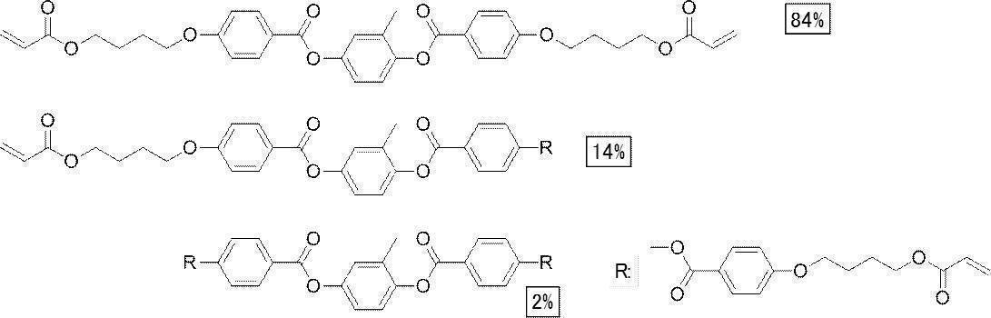
数値は質量%である。また、Rは酸素原子で結合する基である。

実施例1において、コレステリック液晶反射層用塗布液Gm1の界面活性剤F1の量を、表1記載のように変更した以外は同様にして、実施例2~6の加飾シート02~06を作製した。
実施例1において、作製した下塗り層付き透明支持体01を、ラビングロールで搬送方向に平行な方向にクリアランス2.0mm、1000回転/分で回転させてラビング処理を行い、これを表1に記載の回数繰り返した以外は同様にして、実施例7~10の加飾シート07~10を作製した。
なお、ラビングのクリアランス2.0mmの設定は、配向規制力を付与する条件としては弱い条件であり、下塗り層近傍の液晶の配向状態を緩やかに制御するために行なった。
実施例1において、作製した下塗り層付き透明支持体01の表面に、上記で調製したコレステリック液晶反射層用塗布液Gm1をスピンコーターにて、回転数1500rpmで回転時間10秒間塗布し、95℃で60秒乾燥した後、25℃に至るまで、表1に記載の条件で降温し、25℃にて紫外線照射装置により、500mJ/cm2の紫外線を照射した以外は同様にして、実施例11~22の加飾シート11~22を作製した。
実施例1において、作製した下塗り層付き透明支持体01の表面に、上記で調製したコレステリック液晶反射層用塗布液Gm1をスピンコーターにて、表1に記載の回転数で回転時間10秒間塗布し、95℃で60秒乾燥した後、25℃に至るまで、-7℃/秒で降温し、25℃にて紫外線照射装置により、500mJ/cm2の紫外線を照射した以外は同様にして、実施例23~26の加飾シート23~26を作製した。
実施例1の下塗り層付き透明支持体01を用いて下記のように作製した。
<下塗り層02の作製>
下塗り層付き透明支持体01の表面に、下記の組成の下塗り層塗布液02を#3.6のワイヤーバーコーターで塗布した。その後、95℃で60秒乾燥し、25℃にて紫外線照射装置により、500mJ/cm2の紫外線を照射して、下塗り層付き透明支持体02を作製した。
KAYARAD PET30(日本化薬(株)製) 100質量部
IRGACURE 907 (チバガイギー社製) 3.0質量部
カヤキュアーDETX(日本化薬(株)製) 1.0質量部
メチルエチルケトン 120質量部
なお、KAYARAD PET30は、ペンタエリスリトールトリアクリレートと、ペンタエリスリトールテトラアクリレートとの混合物である(PETA)。
実施例1において、作製した下塗り層付き透明支持体01を、ラビングロールで搬送方向に平行な方向にクリアランス1.6mm、1000回転/分で回転させてラビング処理を行い、コレステリック液晶反射層用塗布液Gm1をスピンコーターにて、回転数1500rpmで回転時間10秒間塗布し、95℃で60秒乾燥した後、紫外線照射装置により、500mJ/cm2の紫外線を照射して、比較例1の加飾シート101を作製した。
なお、ラビングのクリアランス1.6mmの設定は、配向規制力を付与する条件としては強い条件であり、下塗り層近傍の液晶の配向状態を強力に制御するために行なった。
実施例1において、コレステリック液晶反射層用塗布液Gm1の界面活性剤F1を添加しなかった以外は同様にして、比較例2の加飾シート102を作製した。
実施例1において、コレステリック液晶反射層用塗布液Gm1の界面活性剤F1を添加せず、代わりに下記構造の界面活性剤F2を0.4質量部添加した以外は同様にして、比較例3の加飾シート103を作製した。
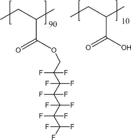
なお、下塗り層として使用したAC-Xとは、ポリエステル系の易接着剤である。
実施例、比較例で作製した各加飾シートに対して、測定、評価を行った結果を下記表1に示す。
形成したコレステリック液晶層の断面SEM写真において、100μm2の領域を任意に10カ所選択し、各領域で構造Aおよび構造Bの数を計数して、10カ所の平均値を、各加飾シートのコレステリック液晶層の断面100μm2当たりの構造Aおよび構造Bの数とした。
上述した特性反射率の測定方法にそって、特性反射率のピーク波長を求めた。なお、実施例、比較例のいずれの加飾シートも、特性反射率のピーク波長は550nm近傍であった。
上述した反射率の測定方法にそって、R[-45,20](λ1)、R[-45,20](λ2)、R[-45,15](λ1)を測定した。
形成したコレステリック液晶層の断面SEM写真において、上述した波打構造のピーク間距離の平均値の測定方法にそって測定を行った。
形成したコレステリック液晶層の断面SEM写真において、コレステリック液晶層の両表面から1μm以内の膜厚内に位置するすべての縞模様を座標化し、膜と平行な方向に0.12μm単位で、55μmに亘り各点の傾き(傾斜角度)を算出した。
各点の傾き(傾斜角度)は、各点を中心に±0.3μm(0.6μm分)の座標データから計算される傾き(傾斜角度)である。これらの傾き(傾斜角度)数値の統計処理から標準偏差を算出し、α、βをそれぞれ測定した。
各加飾シートの5cm×5cmの範囲について、500μmおきに、加飾シートへの極角-45°の入射光に対して、波長λ、極角15°、方位角0°~360°の範囲の受光角度における反射率のRmax[0,15](λ1)、Rmin[0,15](λ1)をそれぞれ求め、Rmax[0,15](λ1)/Rmin[0,15](λ1)が最大となる値を反射率の最大値/最小値として表1に記載した。
上述した積分反射率の測定方法にそって測定を行った。
上述したヘイズの測定方法にそって測定を行い、内部ヘイズ値(Hi)/全ヘイズ値(Ht)を求めた。
上述した表面粗さの測定方法にそって測定を行った。
実施例および比較例の各加飾シートに対して、20名の評価者によって、以下の基準で目視評価させ、その平均点を求め、平均点の小数第一位を四捨五入して光輝性の評価とした。評価の観点は、明室下で照明光の正反射から外れた方向から観察した際の光輝性である。
2:光輝性に乏しい
3:若干の光輝性がある
4:光輝性がある
5:高い光輝性がある
6:極めて高い光輝性がある
7:基準6よりもさらに極めて高い光輝性がある
実施例1において、作製した下塗り層付き透明支持体01の表面に、上記で調製したコレステリック液晶層用塗布液Gm1をスピンコーターにて塗布する際の回転時間を2秒間とした以外は、実施例1と同様にして加飾シート28を作製した。
作製した加飾シート28について、上述した反射率の測定方法にそって、R[-45,20](λ1)、および、R[-45,20](λ2)を測定し、上記と同様にして、加飾シート中心部でのR[-45,20](λ1)/R[-45,20](λ2)、および、同周辺部でのR[-45,20](λ1)/R[-45,20](λ2)を算出した。
この結果、加飾シート中心部では、R[-45,20](λ1)/R[-45,20](λ2)=40.0、周辺部では、R[-45,20](λ1)/R[-45,20](λ2)=40.0であった。
上記作製した加飾シート28に対して、5cm×5cmの範囲について、500μmおきに、加飾シートへの極角-45°の入射光に対して、波長λ、極角15°、方位角0°~360°の範囲の受光角度における反射率のRmax[0,15](λ1)、Rmin[0,15](λ1)をそれぞれ測定し、上記と同様にして、加飾シート中心部での反射率の最大値/最小値、および、同周辺部での反射率の最大値/最小値を算出した。
この結果、加飾シート中心部では反射率の最大値/最小値が1.08であり、周辺部では最大値/最小値が1.3であった。また、加飾シート28は、面内で光輝性にメリハリがあり、加飾用途として意匠性の高い風合いを実現できていた。
(コレステリック液晶反射層用塗布液Gm2の調製)
下記の組成物を調製後、孔径0.2μmのポリプロピレン製フィルタでろ過して、コレステリック液晶反射層用塗布液Gm2として用いた。
LC-1-1は特開2004-12382号公報に記載の方法を元に合成した。LC-1-1は2つの反応性基を有する液晶性化合物であり、2つの反応性基の片方はラジカル性の反応性基であるアクリル基、他方はカチオン性の反応性基であるオキセタン基である。LC-1-2はTetrahedron Lett.誌、第43巻、6793頁(202)に記載の方法に準じて合成した。
コレステリック液晶反射層用塗布液Gm2(質量部)
――――――――――――――――――――――――――――――――
棒状液晶(LC-1-1) 19.57
水平配向剤(LC-1-2) 0.01
カチオン系モノマー
(OXT-121、東亞合成(株)製) 0.98
カチオン系開始剤
(Curacure UVI6974、ダウ・ケミカル製) 0.4
重合制御剤(IRGANOX1076、BASF製) 0.02
上記キラル剤A 1.13
メチルエチルケトン 80.0
―――――――――――――――――――――――――――――――――

下記の組成物を調製後、孔径0.2μmのポリプロピレン製フィルタでろ過して、保護層塗布液AD-1として用いた。
保護層塗布液AD-1(質量部)
―――――――――――――――――――――――――――――――――
ベンジルメタクリレート/メタクリル酸/メタクリル酸メチル
=35.9/22.4/41.7モル比のランダム共重合物
(重量平均分子量3.8万) 8.05
ラジカル光重合開始剤
2-トリクロロメチル-5-(p-スチリルスチリル)
1,3,4-オキサジアゾール) 0.12
ハイドロキノンモノメチルエーテル 0.002
メガファックF-176PF
(大日本インキ化学工業(株)製) 0.05
プロピレングリコールモノメチルエーテルアセテート 34.80
メチルエチルケトン 50.538
メタノール 1.61
―――――――――――――――――――――――――――――――――
実施例1において、作製した下塗り層付き透明支持体01の表面に上記で調製したコレステリック液晶反射層用塗布液Gm2をスピンコーターにて、回転数1500rpmで、回転時間10秒間塗布し、95℃で60秒間加熱熟成し、その後ただちに、膜面温度70℃空気下にて空冷メタルハライドランプ(アイグラフィックス(株)製)を用いて、500mJ/cm2の紫外線を照射し、その配向状態を固定化することにより、パターン作製材料を形成した。
こうして得られたパターン作製材料上に、上記で調製した保護層塗布液AD-1を塗布し、80℃、60秒乾燥した後に、25℃空気下にて、キヤノン(株)製PLA-501F露光機(超高圧水銀ランプ)を用い、50mJ/cm2の露光量で図7または図8に記載のパターンのマスクを介し露光した。その後、基板全体を200℃オーブン内で30分焼成することにより、コレステリック液晶配向による光輝性の高い領域と、光学的等方で透明な領域のある、実施例29の加飾シート29を作製した。
作製した加飾シート29について、上述した反射率の測定方法にそって、R[-45,20](λ1)、および、R[-45,20](λ2)を測定し、上記と同様にしてR[-45,20](λ1)/R[-45,20](λ2)を算出した。その結果、R[-45,20](λ1)/R[-45,20](λ2)=40.0であった。
加飾シート29は、面内で光輝性にメリハリがあり、加飾用途として意匠性の高い風合いを実現できていた。
(コレステリック液晶層用塗布液Gm3)
コレステリック液晶層用塗布液Gm1のメチルエチルケトンをシクロペンタノンに変えた以外は、同様の比率で組成物を調製し、コレステリック液晶層用塗布液Gm3として用いた。
調製したコレステリック液晶反射層用塗布液Gm3を、インクジェットプリンター((株)ミマキエンジニアリング製、JV400SUV)にインクとして装填した。
この時、このインクジェットプリンターが有するマルチドロップ機能を用いて、インク液滴1滴あたりの液量を4pl~40plの範囲でランダムに調節し、かつ、インク液滴の打滴間隔もランダムに調節して、インク液滴に吐出するように設定した。
この設定の下、インクジェットプリンターによって、コレステリック液晶反射層用塗布液Gm2を、下塗り層付き透明支持体01に図7または図8に示すような絵柄で打滴し、95℃で60秒乾燥した後、25℃に至るまで、-7℃/sで降温し、25℃にて紫外線照射装置により、500mJ/cm2の紫外線を照射して、パターニングされた実施例30の加飾シート30を作製した。
作製した加飾シート30について、上述した反射率の測定方法にそって、R[-45,20](λ1)、および、R[-45,20](λ2)を測定し、上記と同様にしてR[-45,20](λ1)/R[-45,20](λ2)を算出した。その結果、R[-45,20](λ1)/R[-45,20](λ2)=40.0であった。
加飾シート30は、面内で光輝性にメリハリがあり、加飾用途として意匠性の高い風合いを実現できていた。
また、文字をパターニングしない全面塗布したものを利用した場合でも、同じ効果が得られた。
・液晶ディスプレイ表面加飾シート(液晶表示装置)
(保護フィルム1の作製)
特開2012-18396の実施例([0267]~[0270])を参考に、セルロースアセテートフィルムを作製した。これを保護フィルム01とする。
特開2012-18396の実施例([0272]~[0282])を参考に、支持体として保護フィルム01を用いて、その上に配向膜と光学異方性層とを形成し、λ/4位相差板を作製した。Re(550)およびRth(550)は、それぞれ130nm、-5nmであった。
作製したλ/4位相差板と、実施例1で作製した加飾シート1の塗布面とを、SKダイン(総研化学(株)製)を用いて貼合し、直線偏光反射偏光子1(複合膜)を作製した。
この液晶表示装置は、液晶ディスプレイの黒表示状態では加飾シート由来の色が綺麗に見えており、白表示状態では透明で存在感が無い状態であった。
・反射レス加飾シート(自動車車内用内装)
ダッシュボードの上に、自動車車内用内装として、直線偏光反射偏光子1を配置し、ダッシュボードの法線とフロントガラスを想定したガラス板の法線とのなす角度が45°になるようにガラス板を設置した。
さらに、観察者の視点およびガラス板の正面の点を結ぶ直線と、鉛直軸のなす平面が直線偏光反射偏光子1とが交わる位置における直線偏光反射偏光子1の反射軸が、上記の平面に対して0°となるように直線偏光反射偏光子1を配置し、ガラス板に対して、P波が入射するようにした。
その結果、ガラス板には、直線偏光反射偏光子1に由来する写りこみは確認できなかった。
2 下塗り層
3,24 支持体
10 加飾シート
Claims (13)
- 波長選択反射性を有するコレステリック液晶層を有し、下記式(1)を満たす加飾シート。
R[-45,20](λ1)/R[-45,20](λ2)≧5 式(1)
ここで、R[-45,20](λ)は、前記加飾シートへの極角-45°の入射光に対して、その入射光の方位角と180°ずれた方位角における極角20°の受光角度で測定される、波長λにおける反射率を表し、
λ1は、前記加飾シートの視認側表面から光が入射するようにして測定される特性反射率の、波長380nm~780nmにおけるピーク波長を表し、
λ21=λ1+200nm、λ22=λ1-200nmとした時、R[-45,20](λ21)とR[-45,20](λ22)を比較して小さい値を示すλ21とλ22のいずれかをλ2とする。 - 下記式(2)を満たす請求項1に記載の加飾シート。
R[-45,20](λ1)/R[-45,15](λ1)≦1.7 式(2)
ここで、R[-45,15](λ)は、前記加飾シートへの極角-45°の入射光に対して、その入射光の方位角と180°ずれた方位角における極角15°の受光角度で測定される、波長λにおける反射率である。 - 前記加飾シートの面内において、下記式(3)を満たす領域Aを有する請求項1または2に記載の加飾シート。
Rmax[0,15](λ1)/Rmin[0,15](λ1)≧1.3 式(3)
ここで、Rmax[0,15](λ)、Rmin[0,15](λ)は、前記加飾シートへの極角0°の入射光に対して、波長λ、極角15°、方位角0°~360°の範囲の受光角度における反射率の最大値、最小値をそれぞれ表す。 - 前記加飾シートの面内において、下記式(4)を満たす領域Bをさらに有する請求項3に記載の加飾シート。
Rmax[0,15](λ1)/Rmin[0,15](λ1)≦1.1 式(4)
ここで、Rmax[0,15](λ)、Rmin[0,15](λ)は、前記加飾シートへの極角0°の入射光に対して、波長λ、極角15°、方位角0°~360°の範囲の受光角度における反射率の最大値、最小値をそれぞれ表す。 - 前記加飾シートの波長380nm~780nmの範囲における正反射成分を除いた積分反射率の最大値が10%以上である請求項1~4のいずれか一項に記載の加飾シート。
- 前記コレステリック液晶層は、断面において走査型電子顕微鏡にて観測される明部と暗部との縞模様を有し、
前記縞模様が波打構造を有しており、
前記波打構造のピーク間距離の平均値が0.5μm~50μmである請求項1~5のいずれか一項に記載の加飾シート。
ここで波打構造とは、縞模様の明部または暗部の連続線において前記コレステリック液晶層の平面に対する傾斜角度の絶対値が5°以上である領域Mが少なくとも一つ存在し、前記領域Mを挟み、最も近い位置にある、2点の傾斜角度0°の山または谷が特定されるものを表す。
また、前記波打構造のピーク間距離とは、前記領域Mを挟み、最も近い位置にある、2点の傾斜角度0°の山または谷について前記コレステリック液晶層の平面方向の距離を計測し、前記コレステリック液晶層の断面長軸方向の長さ100μm、全膜厚において算術平均した値を表す。 - 前記コレステリック液晶層は、断面において走査型電子顕微鏡にて観測される明部と暗部との縞模様を有し、
下記式(5)および(6)をそれぞれ満たす請求項1~6のいずれか一項に記載の加飾シート。
α/β≧1.2 式(5)
α≧2° 式(6)
ここで、α、βはそれぞれ、前記コレステリック液晶層の二つの表面からそれぞれ1μm以内の傾斜角度の各々の標準偏差のうち値が大きい方から2つを表す。
傾斜角度は、前記縞模様の明部または暗部の連続線上の微線分と、前記コレステリック液晶層の法線方向との成す角度を表す。 - 前記加飾シートの全ヘイズ値(Ht)に対する内部ヘイズ値(Hi)の割合が40%以上である請求項1~7のいずれか一項に記載の加飾シート。
- 前記コレステリック液晶層が界面活性剤を有する請求項1~8のいずれか一項に記載の加飾シート。
- 前記コレステリック液晶層は、断面において走査型電子顕微鏡にて観測される明部と暗部との縞模様を有し、
前記明部および前記暗部の少なくとも1本が分岐するものであり、
前記分岐した前記明部および前記暗部において、分岐部から伸びる3本の前記明部または前記暗部のうちの2本の前記明部または前記暗部の間に、前記分岐部に向かう端部を有する前記明部または前記暗部が存在し、
前記分岐部に向かう端部を有する前記明部または前記暗部を間に有する2本の前記明部または前記暗部の間に、1本の前記明部または前記暗部を有する構造を構造A、3本以上の前記明部および前記暗部を有する構造を構造B、とした際に、
前記コレステリック液晶層の断面100μm2当たりに含まれる構造Aおよび構造Bの数が、以下の条件Iおよび条件IIのいずれかを満たす請求項1~9のいずれか一項に記載の加飾シート。
条件I: 前記構造Bを含まず、前記構造Aを0.1個以上50個未満含む。
条件II: 前記構造Bを0.1個以上10個未満含む。 - 下記式(1-1)を満たす請求項1~10のいずれか一項に記載の加飾シート。
R[-45,20](λ1)/R[-45,20](λ2)>9 式(1-1) - 請求項1~11のいずれか一項に記載の加飾シートとλ/4位相差板とを含む複合膜を表面に備える液晶表示装置。
- 請求項1~11のいずれか一項に記載の加飾シートとλ/4位相差板とを含む複合膜を備える自動車車内用内装。
Priority Applications (5)
| Application Number | Priority Date | Filing Date | Title |
|---|---|---|---|
| CN201780053698.5A CN109716181B (zh) | 2016-09-01 | 2017-08-31 | 装饰板、液晶显示装置以及汽车车内用内部装饰 |
| KR1020197004452A KR102189096B1 (ko) | 2016-09-01 | 2017-08-31 | 가식 시트, 액정 표시 장치 및 자동차 차내용 내장 |
| JP2018537417A JP6744415B2 (ja) | 2016-09-01 | 2017-08-31 | 加飾シート、液晶表示装置および自動車車内用内装 |
| EP17846682.7A EP3508894B1 (en) | 2016-09-01 | 2017-08-31 | Decorative sheet, liquid crystal display device, and interior for automobile |
| US16/289,038 US11009754B2 (en) | 2016-09-01 | 2019-02-28 | Decorative sheet, liquid crystal display device and automobile interior material |
Applications Claiming Priority (8)
| Application Number | Priority Date | Filing Date | Title |
|---|---|---|---|
| JP2016-171140 | 2016-09-01 | ||
| JP2016171140 | 2016-09-01 | ||
| JP2016-200848 | 2016-10-12 | ||
| JP2016200848 | 2016-10-12 | ||
| JP2017051263 | 2017-03-16 | ||
| JP2017-051263 | 2017-03-16 | ||
| JP2017135538 | 2017-07-11 | ||
| JP2017-135538 | 2017-07-11 |
Related Child Applications (1)
| Application Number | Title | Priority Date | Filing Date |
|---|---|---|---|
| US16/289,038 Continuation US11009754B2 (en) | 2016-09-01 | 2019-02-28 | Decorative sheet, liquid crystal display device and automobile interior material |
Publications (1)
| Publication Number | Publication Date |
|---|---|
| WO2018043678A1 true WO2018043678A1 (ja) | 2018-03-08 |
Family
ID=61300752
Family Applications (1)
| Application Number | Title | Priority Date | Filing Date |
|---|---|---|---|
| PCT/JP2017/031465 Ceased WO2018043678A1 (ja) | 2016-09-01 | 2017-08-31 | 加飾シート、液晶表示装置および自動車車内用内装 |
Country Status (6)
| Country | Link |
|---|---|
| US (1) | US11009754B2 (ja) |
| EP (1) | EP3508894B1 (ja) |
| JP (1) | JP6744415B2 (ja) |
| KR (1) | KR102189096B1 (ja) |
| CN (1) | CN109716181B (ja) |
| WO (1) | WO2018043678A1 (ja) |
Cited By (14)
| Publication number | Priority date | Publication date | Assignee | Title |
|---|---|---|---|---|
| JP2018200459A (ja) * | 2017-05-29 | 2018-12-20 | 富士フイルム株式会社 | 実像表示用部材、および表示システム |
| JP2020060627A (ja) * | 2018-10-05 | 2020-04-16 | 富士フイルム株式会社 | 光学フィルム、液晶表示装置、自動車社内用内装および光学フィルムの製造方法 |
| JPWO2019035449A1 (ja) * | 2017-08-14 | 2020-07-30 | 富士フイルム株式会社 | 構造体および反射層の形成方法 |
| US20200353652A1 (en) * | 2019-05-10 | 2020-11-12 | Viavi Solutions Inc. | Article including a release layer |
| WO2021010445A1 (ja) * | 2019-07-18 | 2021-01-21 | 富士フイルム株式会社 | 加飾成型体、加飾成型体の製造方法、加飾パネル、及び、電子デバイス |
| JPWO2021153095A1 (ja) * | 2020-01-31 | 2021-08-05 | ||
| JP2021184046A (ja) * | 2020-05-22 | 2021-12-02 | 大日本印刷株式会社 | 光学積層体、位相差フィルム、転写体、光学部材、表示装置、および光学部材の製造方法 |
| JP2022513827A (ja) * | 2018-12-12 | 2022-02-09 | メルク・パテント・ゲゼルシヤフト・ミツト・ベシユレンクテル・ハフツング | 重合性液晶インク配合物 |
| JPWO2022209954A1 (ja) * | 2021-03-30 | 2022-10-06 | ||
| WO2023032520A1 (ja) * | 2021-09-03 | 2023-03-09 | 富士フイルム株式会社 | 積層体、表示装置、自動車および携帯電子機器 |
| WO2023085370A1 (ja) | 2021-11-12 | 2023-05-19 | 富士フイルム株式会社 | 画像記録物及び画像記録方法 |
| US11919327B2 (en) | 2019-03-29 | 2024-03-05 | Fujifilm Corporation | Transfer-type decorative sheet and method of manufacturing transfer-type decorative sheet |
| JP2024095756A (ja) * | 2018-03-23 | 2024-07-10 | 富士フイルム株式会社 | コレステリック液晶層の製造方法、コレステリック液晶層、液晶組成物、硬化物、光学異方体、反射層 |
| US12480050B2 (en) | 2020-01-28 | 2025-11-25 | Fujifilm Corporation | Cholesteric liquid crystal film |
Families Citing this family (3)
| Publication number | Priority date | Publication date | Assignee | Title |
|---|---|---|---|---|
| CN115039000B (zh) * | 2020-01-31 | 2024-09-27 | 富士胶片株式会社 | 胆甾醇型液晶膜及其制造方法 |
| KR102416519B1 (ko) * | 2021-01-21 | 2022-07-05 | 주식회사 제이케이테크 | 기능성 인테리어 필름 |
| JPWO2023248719A1 (ja) * | 2022-06-21 | 2023-12-28 |
Citations (6)
| Publication number | Priority date | Publication date | Assignee | Title |
|---|---|---|---|---|
| WO2015122479A1 (ja) * | 2014-02-14 | 2015-08-20 | 富士フイルム株式会社 | 輝度向上フィルム、光学シート部材および液晶表示装置 |
| JP2016004212A (ja) * | 2014-06-18 | 2016-01-12 | 富士フイルム株式会社 | 反射フィルムおよび反射フィルムを有するディスプレイ |
| WO2016009974A1 (ja) * | 2014-07-15 | 2016-01-21 | 富士フイルム株式会社 | 検知システムおよび検知方法 |
| JP2016071078A (ja) * | 2014-09-29 | 2016-05-09 | 富士フイルム株式会社 | 投映像表示用部材および投映像表示システム |
| WO2016129645A1 (ja) * | 2015-02-10 | 2016-08-18 | 富士フイルム株式会社 | 光学部材、光学素子、液晶表示装置および近接眼光学部材 |
| JP2016149984A (ja) * | 2015-02-18 | 2016-08-22 | 富士フイルム株式会社 | 防虫用反射材、防虫システム、および防虫方法 |
Family Cites Families (17)
| Publication number | Priority date | Publication date | Assignee | Title |
|---|---|---|---|---|
| JP3521916B2 (ja) | 1991-08-29 | 2004-04-26 | 新日本石油株式会社 | コレステリック液晶性フィルムの製造方法 |
| TW289095B (ja) * | 1993-01-11 | 1996-10-21 | ||
| US5541745A (en) * | 1994-01-25 | 1996-07-30 | Fergason; James L. | Illumination system for a display using cholesteric liquid crystal reflectors |
| JP2005049866A (ja) | 2003-07-17 | 2005-02-24 | Dainippon Printing Co Ltd | 位相差層およびそれを用いた液晶表示装置 |
| JP4184189B2 (ja) * | 2003-08-13 | 2008-11-19 | 株式会社 日立ディスプレイズ | 発光型表示装置 |
| JP2006323312A (ja) | 2005-05-20 | 2006-11-30 | Dainippon Printing Co Ltd | 位相差光学素子およびこれを用いた液晶表示装置 |
| JP2007206112A (ja) * | 2006-01-31 | 2007-08-16 | Nippon Zeon Co Ltd | 液晶表示装置 |
| JP2008197223A (ja) | 2007-02-09 | 2008-08-28 | Nippon Zeon Co Ltd | 光学素子、偏光板、位相差板、照明装置、および液晶表示装置 |
| JP4966395B2 (ja) * | 2010-04-14 | 2012-07-04 | 大日本印刷株式会社 | 動画像と静止画像との混用に適した液晶表示装置の黒彩感及び画像の切れの改善方法 |
| GB201019213D0 (en) * | 2010-11-12 | 2010-12-29 | R2Tek Llc | Decorative tile |
| JP2014079944A (ja) * | 2012-10-16 | 2014-05-08 | Geomatec Co Ltd | 電子機器用の保護パネル、その製造方法及び電子機器 |
| CN105359005B (zh) * | 2013-07-05 | 2018-01-12 | 埃西勒国际通用光学公司 | 包括在可见光区具有极低反射的抗反射涂层的光学制品 |
| CN105474291B (zh) * | 2013-08-05 | 2018-06-22 | 夏普株式会社 | 反射镜显示器、半反射镜板和电子设备 |
| WO2015025909A1 (ja) * | 2013-08-21 | 2015-02-26 | 富士フイルム株式会社 | 円偏光フィルターおよびその応用 |
| JPWO2015186297A1 (ja) * | 2014-06-03 | 2017-04-20 | パナソニックIpマネジメント株式会社 | 電子ミラー装置 |
| JP6149006B2 (ja) * | 2014-06-18 | 2017-06-14 | 富士フイルム株式会社 | 反射フィルムおよび反射フィルムを有するディスプレイ |
| JP2016012047A (ja) * | 2014-06-30 | 2016-01-21 | 富士フイルム株式会社 | 液晶表示装置 |
-
2017
- 2017-08-31 WO PCT/JP2017/031465 patent/WO2018043678A1/ja not_active Ceased
- 2017-08-31 JP JP2018537417A patent/JP6744415B2/ja active Active
- 2017-08-31 CN CN201780053698.5A patent/CN109716181B/zh active Active
- 2017-08-31 EP EP17846682.7A patent/EP3508894B1/en active Active
- 2017-08-31 KR KR1020197004452A patent/KR102189096B1/ko active Active
-
2019
- 2019-02-28 US US16/289,038 patent/US11009754B2/en active Active
Patent Citations (6)
| Publication number | Priority date | Publication date | Assignee | Title |
|---|---|---|---|---|
| WO2015122479A1 (ja) * | 2014-02-14 | 2015-08-20 | 富士フイルム株式会社 | 輝度向上フィルム、光学シート部材および液晶表示装置 |
| JP2016004212A (ja) * | 2014-06-18 | 2016-01-12 | 富士フイルム株式会社 | 反射フィルムおよび反射フィルムを有するディスプレイ |
| WO2016009974A1 (ja) * | 2014-07-15 | 2016-01-21 | 富士フイルム株式会社 | 検知システムおよび検知方法 |
| JP2016071078A (ja) * | 2014-09-29 | 2016-05-09 | 富士フイルム株式会社 | 投映像表示用部材および投映像表示システム |
| WO2016129645A1 (ja) * | 2015-02-10 | 2016-08-18 | 富士フイルム株式会社 | 光学部材、光学素子、液晶表示装置および近接眼光学部材 |
| JP2016149984A (ja) * | 2015-02-18 | 2016-08-22 | 富士フイルム株式会社 | 防虫用反射材、防虫システム、および防虫方法 |
Cited By (27)
| Publication number | Priority date | Publication date | Assignee | Title |
|---|---|---|---|---|
| JP2018200459A (ja) * | 2017-05-29 | 2018-12-20 | 富士フイルム株式会社 | 実像表示用部材、および表示システム |
| JPWO2019035449A1 (ja) * | 2017-08-14 | 2020-07-30 | 富士フイルム株式会社 | 構造体および反射層の形成方法 |
| JP7023967B2 (ja) | 2017-08-14 | 2022-02-22 | 富士フイルム株式会社 | 構造体および反射層の形成方法 |
| JP2024095756A (ja) * | 2018-03-23 | 2024-07-10 | 富士フイルム株式会社 | コレステリック液晶層の製造方法、コレステリック液晶層、液晶組成物、硬化物、光学異方体、反射層 |
| JP2020060627A (ja) * | 2018-10-05 | 2020-04-16 | 富士フイルム株式会社 | 光学フィルム、液晶表示装置、自動車社内用内装および光学フィルムの製造方法 |
| JP7058204B2 (ja) | 2018-10-05 | 2022-04-21 | 富士フイルム株式会社 | 光学フィルム、液晶表示装置、自動車社内用内装および光学フィルムの製造方法 |
| US12460134B2 (en) | 2018-12-12 | 2025-11-04 | Merck Patent Gmbh | Polymerizable liquid crystal ink formulations |
| KR102934994B1 (ko) * | 2018-12-12 | 2026-03-09 | 메르크 파텐트 게엠베하 | 중합성 액정 잉크 제형 |
| JP2022513827A (ja) * | 2018-12-12 | 2022-02-09 | メルク・パテント・ゲゼルシヤフト・ミツト・ベシユレンクテル・ハフツング | 重合性液晶インク配合物 |
| US11919327B2 (en) | 2019-03-29 | 2024-03-05 | Fujifilm Corporation | Transfer-type decorative sheet and method of manufacturing transfer-type decorative sheet |
| US20200353652A1 (en) * | 2019-05-10 | 2020-11-12 | Viavi Solutions Inc. | Article including a release layer |
| US11911931B2 (en) * | 2019-05-10 | 2024-02-27 | Viavi Solutions Inc. | Article including a release layer |
| WO2021010445A1 (ja) * | 2019-07-18 | 2021-01-21 | 富士フイルム株式会社 | 加飾成型体、加飾成型体の製造方法、加飾パネル、及び、電子デバイス |
| JPWO2021010445A1 (ja) * | 2019-07-18 | 2021-01-21 | ||
| JP7177273B2 (ja) | 2019-07-18 | 2022-11-22 | 富士フイルム株式会社 | 加飾成型体、加飾成型体の製造方法、加飾パネル、及び、電子デバイス |
| US12480050B2 (en) | 2020-01-28 | 2025-11-25 | Fujifilm Corporation | Cholesteric liquid crystal film |
| JPWO2021153095A1 (ja) * | 2020-01-31 | 2021-08-05 | ||
| JP7662541B2 (ja) | 2020-01-31 | 2025-04-15 | 富士フイルム株式会社 | コレステリック液晶膜及びその製造方法 |
| CN115053157A (zh) * | 2020-01-31 | 2022-09-13 | 富士胶片株式会社 | 胆甾醇型液晶膜及其制造方法 |
| WO2021153095A1 (ja) * | 2020-01-31 | 2021-08-05 | 富士フイルム株式会社 | コレステリック液晶膜及びその製造方法 |
| JP7452244B2 (ja) | 2020-05-22 | 2024-03-19 | 大日本印刷株式会社 | 光学積層体、位相差フィルム、転写体、光学部材、表示装置、および光学部材の製造方法 |
| JP2021184046A (ja) * | 2020-05-22 | 2021-12-02 | 大日本印刷株式会社 | 光学積層体、位相差フィルム、転写体、光学部材、表示装置、および光学部材の製造方法 |
| WO2022209954A1 (ja) * | 2021-03-30 | 2022-10-06 | 富士フイルム株式会社 | 加飾シート、表示装置及び自動車車内用内装 |
| JPWO2022209954A1 (ja) * | 2021-03-30 | 2022-10-06 | ||
| WO2023032520A1 (ja) * | 2021-09-03 | 2023-03-09 | 富士フイルム株式会社 | 積層体、表示装置、自動車および携帯電子機器 |
| WO2023085370A1 (ja) | 2021-11-12 | 2023-05-19 | 富士フイルム株式会社 | 画像記録物及び画像記録方法 |
| US12305044B2 (en) | 2021-11-12 | 2025-05-20 | Fujifilm Corporation | Image recorded material and image recording method |
Also Published As
| Publication number | Publication date |
|---|---|
| CN109716181B (zh) | 2021-03-09 |
| CN109716181A (zh) | 2019-05-03 |
| JPWO2018043678A1 (ja) | 2019-06-24 |
| KR20190026916A (ko) | 2019-03-13 |
| EP3508894B1 (en) | 2020-10-14 |
| KR102189096B1 (ko) | 2020-12-09 |
| JP6744415B2 (ja) | 2020-08-19 |
| EP3508894A1 (en) | 2019-07-10 |
| EP3508894A4 (en) | 2019-10-02 |
| US20190196245A1 (en) | 2019-06-27 |
| US11009754B2 (en) | 2021-05-18 |
Similar Documents
| Publication | Publication Date | Title |
|---|---|---|
| JP6744415B2 (ja) | 加飾シート、液晶表示装置および自動車車内用内装 | |
| JP5525886B2 (ja) | 防眩フィルムの製造方法、防眩フィルム、偏光板、画像表示装置及び透過型/半透過型液晶表示装置 | |
| JP5380029B2 (ja) | 液晶表示装置 | |
| CN101506692B (zh) | 光学层积体、偏振片和图像显示装置 | |
| TW201300819A (zh) | 光學膜、偏光板及成像顯示裝置 | |
| JP2006106715A (ja) | 反射防止フィルム、偏光板、および液晶表示装置 | |
| JP2010237339A (ja) | 光散乱フィルムの製造方法、光散乱フィルム、偏光板、画像表示装置および透過型/半透過型液晶表示装置 | |
| KR20020035607A (ko) | 하나 이상의 입자 함유층을 가진 광학 필름 | |
| WO2010047298A1 (ja) | 光学シート | |
| CN113614592A (zh) | 防反射用圆偏光板和使用其的图像显示装置 | |
| KR20120125206A (ko) | 반사 방지 필름, 편광판 및 액정표시장치 | |
| JPWO2018146995A1 (ja) | 加飾フィルム | |
| JP5559670B2 (ja) | 時分割2眼立体視の透過型液晶表示装置 | |
| JP5286219B2 (ja) | 防眩フィルム及びその製造方法、反射防止フィルム、偏光板、並びに画像表示装置 | |
| CN102870039A (zh) | 液晶显示装置、其制备方法以及图像显示装置 | |
| WO2018212347A1 (ja) | 加飾シート、光学デバイス、画像表示装置 | |
| TW200401920A (en) | Polarizing plate and method for preparing it | |
| WO2010047300A1 (ja) | 光学シート | |
| KR101245436B1 (ko) | 반사 방지 필름의 제조 방법, 반사 방지 필름, 그것을사용한 편광판 및 그것들을 사용한 화상 표시 장치 | |
| JP5604325B2 (ja) | 画像表示装置用表面フィルム、偏光板、及び画像表示装置 | |
| KR20120038701A (ko) | 광학적층체, 편광판 및 표시장치 | |
| JP5857091B2 (ja) | 立体画像表示装置 | |
| TWI442102B (zh) | 濾光片及含有其的液晶顯示器 | |
| KR20120009674A (ko) | 방현 필름, 이를 구비한 편광판 및 표시 장치 | |
| JP2017146367A (ja) | 位相差フィルム |
Legal Events
| Date | Code | Title | Description |
|---|---|---|---|
| 121 | Ep: the epo has been informed by wipo that ep was designated in this application |
Ref document number: 17846682 Country of ref document: EP Kind code of ref document: A1 |
|
| ENP | Entry into the national phase |
Ref document number: 20197004452 Country of ref document: KR Kind code of ref document: A |
|
| ENP | Entry into the national phase |
Ref document number: 2018537417 Country of ref document: JP Kind code of ref document: A |
|
| NENP | Non-entry into the national phase |
Ref country code: DE |
|
| ENP | Entry into the national phase |
Ref document number: 2017846682 Country of ref document: EP Effective date: 20190401 |