WO2018029971A1 - デバイス検査回路、デバイス検査装置及びプローブカード - Google Patents
デバイス検査回路、デバイス検査装置及びプローブカード Download PDFInfo
- Publication number
- WO2018029971A1 WO2018029971A1 PCT/JP2017/021556 JP2017021556W WO2018029971A1 WO 2018029971 A1 WO2018029971 A1 WO 2018029971A1 JP 2017021556 W JP2017021556 W JP 2017021556W WO 2018029971 A1 WO2018029971 A1 WO 2018029971A1
- Authority
- WO
- WIPO (PCT)
- Prior art keywords
- operational amplifier
- power supply
- resistor
- inspection circuit
- flow path
- Prior art date
- Legal status (The legal status is an assumption and is not a legal conclusion. Google has not performed a legal analysis and makes no representation as to the accuracy of the status listed.)
- Ceased
Links
Images




Classifications
-
- G—PHYSICS
- G01—MEASURING; TESTING
- G01R—MEASURING ELECTRIC VARIABLES; MEASURING MAGNETIC VARIABLES
- G01R19/00—Arrangements for measuring currents or voltages or for indicating presence or sign thereof
- G01R19/165—Indicating that current or voltage is either above or below a predetermined value or within or outside a predetermined range of values
- G01R19/16533—Indicating that current or voltage is either above or below a predetermined value or within or outside a predetermined range of values characterised by the application
- G01R19/16538—Indicating that current or voltage is either above or below a predetermined value or within or outside a predetermined range of values characterised by the application in AC or DC supplies
- G01R19/16552—Indicating that current or voltage is either above or below a predetermined value or within or outside a predetermined range of values characterised by the application in AC or DC supplies in I.C. power supplies
-
- G—PHYSICS
- G01—MEASURING; TESTING
- G01R—MEASURING ELECTRIC VARIABLES; MEASURING MAGNETIC VARIABLES
- G01R31/00—Arrangements for testing electric properties; Arrangements for locating electric faults; Arrangements for electrical testing characterised by what is being tested not provided for elsewhere
- G01R31/28—Testing of electronic circuits, e.g. by signal tracer
- G01R31/2851—Testing of integrated circuits [IC]
- G01R31/2855—Environmental, reliability or burn-in testing
- G01R31/2872—Environmental, reliability or burn-in testing related to electrical or environmental aspects, e.g. temperature, humidity, vibration, nuclear radiation
- G01R31/2879—Environmental, reliability or burn-in testing related to electrical or environmental aspects, e.g. temperature, humidity, vibration, nuclear radiation related to electrical aspects, e.g. to voltage or current supply or stimuli or to electrical loads
-
- G—PHYSICS
- G01—MEASURING; TESTING
- G01R—MEASURING ELECTRIC VARIABLES; MEASURING MAGNETIC VARIABLES
- G01R1/00—Details of instruments or arrangements of the types included in groups G01R5/00 - G01R13/00 and G01R31/00
- G01R1/20—Modifications of basic electric elements for use in electric measuring instruments; Structural combinations of such elements with such instruments
- G01R1/203—Resistors used for electric measuring, e.g. decade resistors standards, resistors for comparators, series resistors, shunts
-
- G—PHYSICS
- G01—MEASURING; TESTING
- G01R—MEASURING ELECTRIC VARIABLES; MEASURING MAGNETIC VARIABLES
- G01R1/00—Details of instruments or arrangements of the types included in groups G01R5/00 - G01R13/00 and G01R31/00
- G01R1/02—General constructional details
- G01R1/06—Measuring leads; Measuring probes
- G01R1/067—Measuring probes
- G01R1/073—Multiple probes
- G01R1/07307—Multiple probes with individual probe elements, e.g. needles, cantilever beams or bump contacts, fixed in relation to each other, e.g. bed of nails fixture or probe card
-
- G—PHYSICS
- G01—MEASURING; TESTING
- G01R—MEASURING ELECTRIC VARIABLES; MEASURING MAGNETIC VARIABLES
- G01R1/00—Details of instruments or arrangements of the types included in groups G01R5/00 - G01R13/00 and G01R31/00
- G01R1/02—General constructional details
- G01R1/06—Measuring leads; Measuring probes
- G01R1/067—Measuring probes
- G01R1/073—Multiple probes
- G01R1/07307—Multiple probes with individual probe elements, e.g. needles, cantilever beams or bump contacts, fixed in relation to each other, e.g. bed of nails fixture or probe card
- G01R1/07342—Multiple probes with individual probe elements, e.g. needles, cantilever beams or bump contacts, fixed in relation to each other, e.g. bed of nails fixture or probe card the body of the probe being at an angle other than perpendicular to test object, e.g. probe card
-
- G—PHYSICS
- G01—MEASURING; TESTING
- G01R—MEASURING ELECTRIC VARIABLES; MEASURING MAGNETIC VARIABLES
- G01R19/00—Arrangements for measuring currents or voltages or for indicating presence or sign thereof
-
- G—PHYSICS
- G01—MEASURING; TESTING
- G01R—MEASURING ELECTRIC VARIABLES; MEASURING MAGNETIC VARIABLES
- G01R31/00—Arrangements for testing electric properties; Arrangements for locating electric faults; Arrangements for electrical testing characterised by what is being tested not provided for elsewhere
- G01R31/26—Testing of individual semiconductor devices
-
- G—PHYSICS
- G01—MEASURING; TESTING
- G01R—MEASURING ELECTRIC VARIABLES; MEASURING MAGNETIC VARIABLES
- G01R31/00—Arrangements for testing electric properties; Arrangements for locating electric faults; Arrangements for electrical testing characterised by what is being tested not provided for elsewhere
- G01R31/26—Testing of individual semiconductor devices
- G01R31/2607—Circuits therefor
-
- G—PHYSICS
- G01—MEASURING; TESTING
- G01R—MEASURING ELECTRIC VARIABLES; MEASURING MAGNETIC VARIABLES
- G01R31/00—Arrangements for testing electric properties; Arrangements for locating electric faults; Arrangements for electrical testing characterised by what is being tested not provided for elsewhere
- G01R31/28—Testing of electronic circuits, e.g. by signal tracer
-
- G—PHYSICS
- G01—MEASURING; TESTING
- G01R—MEASURING ELECTRIC VARIABLES; MEASURING MAGNETIC VARIABLES
- G01R31/00—Arrangements for testing electric properties; Arrangements for locating electric faults; Arrangements for electrical testing characterised by what is being tested not provided for elsewhere
- G01R31/28—Testing of electronic circuits, e.g. by signal tracer
- G01R31/282—Testing of electronic circuits specially adapted for particular applications not provided for elsewhere
- G01R31/2831—Testing of materials or semi-finished products, e.g. semiconductor wafers or substrates
-
- G—PHYSICS
- G01—MEASURING; TESTING
- G01R—MEASURING ELECTRIC VARIABLES; MEASURING MAGNETIC VARIABLES
- G01R31/00—Arrangements for testing electric properties; Arrangements for locating electric faults; Arrangements for electrical testing characterised by what is being tested not provided for elsewhere
- G01R31/28—Testing of electronic circuits, e.g. by signal tracer
- G01R31/2851—Testing of integrated circuits [IC]
- G01R31/2884—Testing of integrated circuits [IC] using dedicated test connectors, test elements or test circuits on the IC under test
-
- G—PHYSICS
- G01—MEASURING; TESTING
- G01R—MEASURING ELECTRIC VARIABLES; MEASURING MAGNETIC VARIABLES
- G01R31/00—Arrangements for testing electric properties; Arrangements for locating electric faults; Arrangements for electrical testing characterised by what is being tested not provided for elsewhere
- G01R31/28—Testing of electronic circuits, e.g. by signal tracer
- G01R31/317—Testing of digital circuits
- G01R31/3181—Functional testing
- G01R31/319—Tester hardware, i.e. output processing circuits
-
- G—PHYSICS
- G01—MEASURING; TESTING
- G01R—MEASURING ELECTRIC VARIABLES; MEASURING MAGNETIC VARIABLES
- G01R19/00—Arrangements for measuring currents or voltages or for indicating presence or sign thereof
- G01R19/0092—Measuring current only
Definitions
- the present invention relates to a device inspection circuit, a device inspection apparatus, and a probe card for inspecting a semiconductor device formed on a substrate.
- a device for inspecting a semiconductor device formed on a semiconductor wafer as a substrate (hereinafter simply referred to as “wafer”) without cutting out from the wafer in order to find defects or the like at an early stage in the manufacturing process of the semiconductor device.
- a prober an inspection device, has been developed.
- the prober includes a probe card having a large number of pin-shaped probes, and a stage on which a wafer is placed and moves freely up and down, left and right.
- Each probe of the probe card is a semiconductor device to be inspected (Device Under Test, hereinafter
- the DUT is contacted with an electrode pad or a solder bump, and a signal from the DUT is transmitted to an LSI tester provided on the prober to inspect the electrical characteristics of the DUT (see, for example, Patent Document 1). .
- a prober for simultaneously inspecting electrical characteristics of a plurality of DUTs formed on a wafer has been developed.
- a power source 101 that supplies power to the DUT 100 is provided corresponding to each DUT 100.
- the number of DUTs formed on a wafer has increased significantly from the viewpoint of increasing the diameter of the wafer and improving the production efficiency of semiconductor devices. For example, it may exceed 1000.
- the power supply 101 is provided in the LSI tester. Even in this case, it is difficult to provide the power supply 101 in the LSI tester corresponding to each of the DUTs 100 due to layout restrictions in the LSI tester. Increase the cost of LSI testers.
- the power supply circuit 102 includes an operational amplifier for amplifying the power supplied from the power supply 101.
- the current flowing through the DUT 100 (hereinafter referred to as “device current”) has the same value as the current flowing through the power supply 101. Therefore, the current flowing through the power supply 101 using the current measurement function of the power supply 101 is used as the device current.
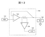
- the power supply circuit 102 when the power supply circuit 102 is provided, an operational amplifier is interposed between the power supply 101 and the DUT 100, so that the device current and the current flowing through the power supply 101 are not the same value. Accordingly, in the power supply circuit 102, as shown in FIG. 12, the sense amplifier 104 and the AD converter 105 are arranged between the operational amplifier 103 and the DUT 100, and the operational amplifier 103 and the DUT 100 are used to move from the operational amplifier 103 to the DUT 100. It is necessary to directly measure the flowing current.
- An object of the present invention is to provide a device inspection circuit, a device inspection apparatus, and a probe card that can measure currents flowing through a large number of devices without increasing costs.
- a power supply having a current measurement function, an operational amplifier, and a first resistor are provided, and the power supply, the operational amplifier, the first resistance, and a device are connected in series in this order.
- a device inspection circuit for connecting the power supply to a non-inverting input terminal of the operational amplifier, wherein a first feedback flow path for applying a voltage between the first resistor and the device to the inverting input terminal of the operational amplifier.
- a second feedback flow path for connecting a point between the operational amplifier and the first resistor and a non-inverting input terminal of the operational amplifier, and the second feedback flow path has a second resistance.
- a device inspection circuit is provided.
- the negative feedback operation of the operational amplifier causes the potential of the non-inverting input terminal of the operational amplifier to be the first resistor and device. Is equal to the potential between.
- the second feedback flow path connects the point between the operational amplifier and the first resistor and the non-inverting input terminal of the operational amplifier, the voltage drop margin in the second feedback flow path is the voltage drop margin in the first resistance. Is equal to Furthermore, the current flowing through the second return channel can be measured using a current measurement function of the power supply.
- the current flowing through the first resistor can be calculated based on the first resistor, the second resistor, and the current flowing through the second feedback flow path.
- the current flowing from the first resistor toward the device can be calculated without providing a sense amplifier or an AD converter corresponding to each device. That is, current flowing through a large number of devices can be measured without increasing costs.
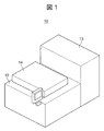
- FIG. 1 It is a perspective view for demonstrating roughly the structure of the prober as a device inspection apparatus which concerns on the 1st Embodiment of this invention.
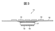
- FIG. 1 It is a front view for demonstrating schematically the structure of the prober of FIG. It is an enlarged front view which shows the structure of the probe card in FIG.
- FIG. 5 is a circuit diagram for explaining a correspondence relationship between a power supply and each DUT when power is supplied from one power supply to a plurality of DUTs. It is a circuit diagram which shows the structure of the normal electric power supply circuit in the case of supplying electric power from one power supply to several DUT.
- FIG. 1 is a perspective view for schematically explaining the configuration of a prober as a device inspection apparatus according to the present embodiment
- FIG. 2 is a front view thereof.
- FIG. 2 is partially drawn as a cross-sectional view and shows components incorporated in a main body 12, a loader 13 and a test box 14 to be described later.
- the prober 10 includes a main body 12 containing a stage 11 on which a wafer W is placed, a loader 13 arranged adjacent to the main body 12, and a test arranged so as to cover the main body 12.
- the main body 12 has a hollow casing shape, and in addition to the stage 11 described above, a probe card 15 is disposed so as to face the stage 11, and the probe card 15 faces the wafer W.
- the probe card 15 includes a plate-shaped card board 16 and a probe head 17 disposed on the lower surface of the card board 16 facing the wafer W. As shown in FIG. 3, the probe head 17 has a large number of needle-like probes 18 corresponding to the electrode pads and solder bumps of each DUT formed on the wafer W.
- the wafer W is fixed to the stage 11 so that the relative position with respect to the stage 11 does not shift.
- the stage 11 is movable in the horizontal direction and the vertical direction, and adjusts the relative positions of the probe card 15 and the wafer W to accurately bring the electrode pads and solder bumps of each DUT into contact with the probes 18 of the probe head 17.
- the loader 13 takes out a wafer W on which a large number of DUTs are formed from a FOUP (not shown) as a transfer container and places the wafer W on the stage 11 inside the main body 12.
- a card-side inspection circuit 19 is formed on the card board 16 of the probe card 15 (see FIG. 3), and the card-side inspection circuit 19 is connected to the probe head 17.
- the test box 14 has a wiring harness 20 and a test board 22 on which a box side inspection circuit 21 (device inspection circuit) is formed.
- the harness 20 connects the test board 22 of the test box 14 and the card board 16 of the probe card 15.
- the card side inspection circuit 19 and the box side inspection circuit 21 reproduce a part of the circuit configuration of the motherboard on which the semiconductor device is mounted.
- the loader 13 includes a base unit 23 including a power source, a controller, and a simple measurement module.
- the base unit 23 is connected to the box side inspection circuit 21 by the wiring 24, and the controller instructs the box side inspection circuit 21 to start inspection of the electrical characteristics of the DUT.
- the box side inspection circuit 21 When inspecting the electrical characteristics of the DUT, the box side inspection circuit 21 supplies power to each DUT via the card side inspection circuit 19 and the probe card 15 and transmits data to the card side inspection circuit 19. Further, the box side inspection circuit 21 determines whether or not the transmitted data has been correctly processed by the card side inspection circuit 19 connected to each DUT based on the electrical signal from the card side inspection circuit 19.
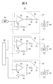
- FIG. 4 is a circuit diagram showing a configuration of the box side inspection circuit in FIG. In FIG. 4, only components related to power supply are shown.
- the box side inspection circuit 21 includes a power supply 25 having a current measurement function, a plurality of power supply circuits 27 connected to each DUT 26 formed on the wafer W on a one-to-one basis, and a switch control unit 28. .
- the power supply 25 is branched and connected to a plurality of power supply circuits 27, and the power from the power supply 25 is divided and supplied to each power supply circuit 27.
- Each power supply circuit 27 includes an operational amplifier 29 and a sense resistor 30 (first resistor). In the box-side inspection circuit 21, the power supply 25, the operational amplifier 29, the sense resistor 30, the probe 18 and the DUT 26 are arranged in this order.
- each power supply circuit 27 includes a negative feedback channel 32 (first feedback channel) that connects a downstream sense point 31 existing between the sense resistor 30 and the DUT 26 and the inverting input terminal of the operational amplifier 29, and an operational amplifier 29. And an upstream sense point 33 existing between the sense resistor 30 and a positive feedback flow path 34 (second feedback flow path) connecting the non-inverting input terminal of the operational amplifier 29.
- the negative feedback flow path 32 applies the voltage at the downstream sense point 31, that is, the voltage between the sense resistor 30 and the DUT 26 to the inverting input terminal of the operational amplifier 29.
- the positive feedback flow path 34 includes a feedback resistor 35 (second resistance) and a switch 36 that can cut off the positive feedback flow path 34 by an on / off operation.
- the switch 36 is connected to the switch control unit 28 to perform switch control.
- the unit 28 controls the on / off operation of the switch 36.
- the switch 36 is normally turned off.
- the voltage drop margin in the positive feedback flow path 34 is the same as the difference between the potential at the upstream sense point 33 and the potential at the downstream sense point 31, that is, the voltage drop margin at the sense resistor 30.
- the resistance value of the sense resistor 30 is R 1 ( ⁇ )
- the current flowing through the sense resistor 30 is I 1 (A)
- the resistance value of the feedback resistor 35 is R 2 ( ⁇ )
- the box-side inspection circuit 21 can calculate the device current flowing through the sense resistor 30 without providing a sense amplifier or an AD converter corresponding to each DUT 26. That is, it is possible to measure the current flowing through the multiple DUTs 26 formed on the wafer W without increasing the cost of the prober.
- one power supply 25 is connected to the non-inverting input terminal of the operational amplifier 29 of the plurality of power supply circuits 27, and the plurality of power supply circuits 27 are connected to the plurality of DUTs 26 on a one-to-one basis. Electric power can be supplied from a single power supply 25 to a plurality of DUTs 26. Thus, the number of power supplies 25 can be reduced to further reduce costs.
- the feedback current I 2 in the positive feedback flow path 34 of each power supply circuit 27 is measured by the current measurement function of the power supply 25, but one power supply 25 is connected to a plurality of power supply circuits 27. Therefore, there is a possibility that the power supply 25 measures a plurality of feedback currents I 2 at the same time.
- the positive feedback flow path 34 has a switch 36. by controlling the operation of the switch 36, only one of positive feedback channel 34 can flow a feedback current I 2, preventing the result, that the power supply 25 will be measured a plurality of feedback current I 2 at the same time can do. Further, by sequentially turning on each switch 36 of the positive feedback channel 34 in each of the power supply circuit 27, it is possible to successively measure the feedback current I 2 in all of the power supply circuit 27, as a result, all The device current of the DUT 26 can be calculated.
- one power source 25 is shown in the box side inspection circuit 21, but the number of power sources 25 included in the box side inspection circuit 21 is not limited to one.
- three power supply circuits 27 are connected to the power supply 25, but the number of power supply circuits 27 connected to the power supply 25 is not limited to three.
- FIG. 5 is a circuit diagram showing the configuration of the power supply circuit in the device inspection circuit according to the second embodiment of the present invention.
- the power supply circuit 37 has a bypass flow path 38 (avoidance flow path) that avoids the sense resistor 30 and directly connects the operational amplifier 29 and the DUT 26.
- the bypass flow path 38 has a diode 39, and the diode 39 is connected in parallel with the sense resistor 30.
- the diode 39 rapidly allows current to pass when the voltage drop in the sense resistor 30, that is, the potential difference between the voltages applied to the diode 39 exceeds a predetermined value.
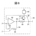
- FIG. 6 is a circuit diagram showing the configuration of the power supply circuit in the device inspection circuit according to the third embodiment of the present invention.
- the power supply circuit 40 includes a transistor 41 made of a bipolar transistor and an additional power supply (other power supply) (not shown) that supplies a relatively large amount of power.
- the base of the transistor 41 is connected between the operational amplifier 29 and the sense resistor 30, and the emitter of the transistor 41 is connected between the sense resistor 30 and the DUT 26. That is, the transistor 41 is arranged in parallel with the sense resistor 30.
- a potential difference corresponding to the voltage drop in the sense resistor 30 is generated between the base and emitter of the transistor 41 and a base current flows.
- An additional power source is connected to the collector of the transistor 41 via a limiter circuit 42 (current limiting circuit).
- a limiter circuit 42 current limiting circuit
- the limiter circuit 42 is interposed between the additional power source and the transistor 41, it is possible to prevent a large current from flowing from the additional power source to the DUT 26 even when the DUT 26 is short-circuited. , The DUT 26 can be prevented from being destroyed.
- a bipolar transistor is used as the transistor 41.
- a field effect transistor may be used.
- the gate of the transistor 41 is connected between the operational amplifier 29 and the sense resistor 30, and the source of the transistor 41 is connected between the sense resistor 30 and the DUT 26.
- an additional power source is connected to the drain of the transistor 41 via a limiter circuit 42.
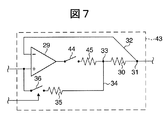
- FIG. 7 is a circuit diagram showing the configuration of the power supply circuit in the device inspection circuit according to the fourth embodiment of the present invention.
- one power supply 25 divides and supplies power to a plurality of DUTs 26, but when a failure occurs in one DUT 26 of the plurality of DUTs 26, power is supplied to the DUT 26. If the DUT 26 continues to be supplied, the DUT 26 may be destroyed. Therefore, the power supply 25 needs to stop supplying power to the DUT 26 in which a problem has occurred. However, if the supply of power from the power source 25 is stopped, the supply of power to the other DUTs 26 is also stopped. Therefore, the electrical characteristics of the other DUTs 26 that are not defective cannot be inspected, and the inspection efficiency of each DUT 26 is reduced. There is a risk of degrading.
- the power supply circuit 43 has an additional switch 44 (another switch) interposed between the operational amplifier 29 and the sense resistor 30.
- an additional switch 44 another switch
- the power supply circuit 43 has an auxiliary resistor 45 (third resistor) interposed between the additional switch 44 and the sense resistor 30, and the upstream sense point 33 is arranged between the auxiliary resistor 45 and the sense resistor 30. Is done.
- the voltage drop margin in the positive feedback flow path 34 is the difference between the potential lowered by the auxiliary resistor 45 and the potential of the non-inverting input terminal of the operational amplifier 29. That is, the voltage drop margin in the positive feedback flow path 34 can be reduced, and for example, it is possible to prevent an excessive current from flowing in the positive feedback flow path 34 and the feedback resistor 35 from abnormally generating heat.
- an auxiliary resistor 45 is connected in series to the operational amplifier 29 in addition to the sense resistor 30. As a result, the current flowing to the operational amplifier 29 can be limited, thereby preventing an excessive current from flowing through the operational amplifier 29 and causing the operational amplifier 29 to generate abnormal heat.
- the operational amplifier 29, the additional switch 44, the auxiliary resistor 45, and the sense resistor 30 are connected in series in this order, but the upstream sense point 33 is disposed between the auxiliary resistor 45 and the sense resistor 30.
- the order of the additional switch 44 and the auxiliary resistor 45 may be changed as long as possible.
- the fifth embodiment is basically the same in configuration and operation as the first embodiment described above, the description of the duplicated configuration and operation is omitted, and the different configuration and operation are described below. Give an explanation.
- FIG. 8 is a circuit diagram showing the configuration of the power supply circuit in the device inspection circuit according to the fifth embodiment of the present invention.
- one power supply 25 divides and supplies power to a plurality of DUTs 26, but when the number of DUTs 26 to which one power supply 25 supplies power increases, the standby of each DUT 26 Sometimes, even if sufficient power can be supplied to each DUT 26, there is a possibility that sufficient power cannot be supplied to each DUT 26 when each DUT 26 operates.
- the power supply circuit 46 includes a transistor 47 made of a bipolar transistor and another additional power source (not shown) that supplies a relatively large amount of power.
- the transistor 47 is interposed between the operational amplifier 29 and the sense resistor 30, the base of the transistor 47 is connected to the operational amplifier 29, and the emitter of the transistor 47 is connected to the sense resistor 30. Accordingly, a base current flows between the base and emitter of the transistor 41 due to the potential difference between the operational amplifier 29 and the sense resistor 30.
- another additional power source is connected to the collector of the transistor 47 via a limiter circuit 48.
- a bipolar transistor is used as the transistor 47, but a field effect transistor may be used.
- the gate of the transistor 47 is connected to the operational amplifier 29 and the source of the transistor 47 is connected to the sense resistor 30.
- another additional power source is connected to the drain of the transistor 47 via a limiter circuit 48.
- the power supply may be amplified using the operational amplifier 29 when the power supplied to the power supply 25 is small.
- the power supply circuit 49 having substantially the same configuration as that of the power supply circuit 40 is used.
- the power supply 25 has no possibility of simultaneously measuring a plurality of feedback currents I 2 , As shown in FIG. 9, it is not necessary to provide the switch 36 in the positive feedback flow path 34, and further, it is not necessary to provide the switch control unit 28. Thereby, the configuration of the power supply circuit 49 can be simplified as compared with the power supply circuit 40.
- the power supply circuit 27 (37, 40, 43, 46, 49) is formed in the box side inspection circuit 21 of the test box 14, but the power supply circuit 27 (37, 40, 49) is formed. 43, 46, 49) may be formed in the card side inspection circuit 19 of the probe card 15.
Landscapes
- Physics & Mathematics (AREA)
- General Physics & Mathematics (AREA)
- Engineering & Computer Science (AREA)
- General Engineering & Computer Science (AREA)
- Computer Hardware Design (AREA)
- Microelectronics & Electronic Packaging (AREA)
- Environmental & Geological Engineering (AREA)
- Power Engineering (AREA)
- Health & Medical Sciences (AREA)
- Toxicology (AREA)
- Testing Or Measuring Of Semiconductors Or The Like (AREA)
- Tests Of Electronic Circuits (AREA)
Abstract
コストを上昇させること無く、多数のデバイスを流れる電流を測定することができるデバイス検査回路を提供する。ボックス側検査回路21の電力供給回路27は、オペアンプ29及びセンス抵抗30を備え、電流測定機能を有する電源25、オペアンプ29、センス抵抗30及びDUT26をこの順で直列に接続し、電源25をオペアンプ29の非反転入力端子に接続し、さらに、電力供給回路27は、センス抵抗30及びDUT26の間の電圧をオペアンプ29の反転入力端子に印加する負帰還流路32と、オペアンプ29及びセンス抵抗30の間の上流センスポイント33並びにオペアンプ29の非反転入力端子を接続する正帰還流路34とを備え、正帰還流路34は帰還抵抗35を有する。
Description
本発明は、基板に形成された半導体デバイスを検査するためのデバイス検査回路、デバイス検査装置及びプローブカードに関する。
半導体デバイスの製造工程における早い段階で欠陥等を発見するために、基板としての半導体ウエハ(以下、単に「ウエハ」という。)に形成された半導体デバイスを当該ウエハから切り出すこと無く検査するためのデバイス検査装置であるプローバが開発されている。
プローバは、多数のピン状のプローブを有するプローブカードと、ウエハを載置して上下左右に自在に移動するステージとを備え、プローブカードの各プローブを検査対象の半導体デバイス(Device Under Test、以下「DUT」という。)が有する電極パッドや半田バンプに接触させ、DUTからの信号をプローバ上に設けられるLSIテスタへ伝達させてDUTの電気的特性を検査する(例えば、特許文献1参照。)。
特に、検査効率を向上させてスループットを向上させる観点から、ウエハに形成された複数のDUTの電気的特性を同時に検査するプローバが開発されている。このようなプローバでは、通常、図10に示すように、DUT100の1つ1つに対応して当該DUT100へ電力を供給する電源101が設けられている。
近年、ウエハの大口径化や半導体デバイスの生産効率向上の観点からウエハに形成されるDUTの数は大幅に増加し、例えば、1000個を超えることがある。このとき、DUT100の1つ1つに対応してプローバに電源101を設けることは、プローバ内におけるレイアウト上の制約から困難であり、プローバのコストを上昇させる。また、電源101をLSIテスタに設ける場合もあるが、この場合でも、DUT100の1つ1つに対応してLSIテスタに電源101を設けることは、LSIテスタ内におけるレイアウト上の制約から困難であり、LSIテスタのコストを上昇させる。
そこで、図11に示すように、1つの電源101から複数のDUT100へ電力を供給することが検討されている。この場合、各DUT100へ供給される電力を制御するために各DUT100に対応して電力供給回路102が設けられるが、各DUT100へ供給される電力が不足し、各DUT100の印加電圧が低下する可能性があるため、電力供給回路102は電源101から供給される電力を増幅するためのオペアンプを有する。
ところで、従来、DUT100を流れる電流(以下、「デバイス電流」という。)は電源101を流れる電流と同値であることから、電源101が有する電流測定機能を用いて電源101を流れる電流をデバイス電流として測定していたが、電力供給回路102が設けられる場合、電源101及びDUT100の間にオペアンプが介在することになるため、デバイス電流と電源101を流れる電流は同値とならない。したがって、電力供給回路102において、図12に示すように、オペアンプ103及びDUT100の間にセンスアンプ104やADコンバータ105を配置し、センスアンプ104やADコンバータ105を用いてオペアンプ103からDUT100へ向けて流れる電流を直接測定する必要がある。
しかしながら、センスアンプ104やADコンバータ105は1つのDUT100に対応して1つずつ設ける必要があるところ、上述したような、ウエハに形成されるDUTの数が1000個を超える場合、DUTの数に対応して同数のセンスアンプ104やADコンバータ105を設けることは、プローバ内におけるレイアウト上の制約から困難であり、結果として、多数のDUTを流れる電流の測定は困難となる。また、多数のセンスアンプ104やADコンバータ105の存在がプローバのコストを上昇させるという問題が生じる。
本発明の目的は、コストを上昇させること無く、多数のデバイスを流れる電流を測定することができるデバイス検査回路、デバイス検査装置及びプローブカードを提供することにある。
上記目的を達成するために、本発明によれば、電流測定機能を有する電源、オペアンプ及び第1の抵抗を備え、前記電源、前記オペアンプ、前記第1の抵抗及びデバイスをこの順で直列に接続し、前記電源を前記オペアンプの非反転入力端子に接続するデバイス検査回路であって、前記第1の抵抗及び前記デバイスの間の電圧を前記オペアンプの反転入力端子に印加する第1の帰還流路と、前記オペアンプ及び前記第1の抵抗の間のポイント並びに前記オペアンプの非反転入力端子を接続する第2の帰還流路とをさらに備え、前記第2の帰還流路は第2の抵抗を有するデバイス検査回路が提供される。
本発明によれば、第1の抵抗及びデバイスの間の電圧がオペアンプの反転入力端子に印加されるため、オペアンプの負帰還動作により、オペアンプの非反転入力端子の電位が第1の抵抗及びデバイスの間の電位と等しくなる。また、第2の帰還流路はオペアンプ及び第1の抵抗の間のポイント並びにオペアンプの非反転入力端子を接続するため、第2の帰還流路における電圧降下代は第1の抵抗における電圧降下代と等しくなる。さらに、第2の帰還流路を流れる電流は電源が有する電流測定機能を用いて測定することができる。したがって、オームの法則により、第1の抵抗、第2の抵抗及び第2の帰還流路を流れる電流に基づいて第1の抵抗を流れる電流を算出することができる。その結果、各デバイスに対応してセンスアンプやADコンバータを設けること無く、第1の抵抗からデバイスへ向けて流れる電流を算出することができる。すなわち、コストを上昇させること無く、多数のデバイスを流れる電流を測定することができる。
以下、本発明の実施の形態について図面を参照しながら説明する。
まず、本発明の第1の実施の形態について説明する。
図1は、本実施の形態に係るデバイス検査装置としてのプローバの構成を概略的に説明するための斜視図であり、図2は、同正面図である。図2は部分的に断面図として描かれ、後述する本体12、ローダ13及びテストボックス14に内蔵される構成要素が示される。
図1及び図2において、プローバ10は、ウエハWを載置するステージ11を内蔵する本体12と、該本体12に隣接して配置されるローダ13と、本体12を覆うように配置されるテストボックス14とを備え、ウエハWに形成された多数のDUTの電気的特性の検査を同時に行う。本体12は内部が空洞の筐体形状を呈し、当該内部には上述したステージ11の他に、該ステージ11に対向するようにプローブカード15が配置され、プローブカード15はウエハWと対向する。プローブカード15は、板状のカードボード16と、カードボード16におけるウエハWと対向する下面に配置されるプローブヘッド17とを有する。図3に示すように、プローブヘッド17はウエハWに形成された各DUTの電極パッドや半田バンプに対応する多数の針状のプローブ18を有する。
ウエハWはステージ11に対する相対位置がずれないように該ステージ11へ固定される。ステージ11は水平方向及び上下方向に関して移動可能であり、プローブカード15及びウエハWの相対位置を調整して各DUTの電極パッドや半田バンプをプローブヘッド17の各プローブ18へ正確に接触させる。ローダ13は、搬送容器であるFOUP(図示しない)から多数のDUTが形成されたウエハWを取り出して本体12の内部のステージ11へ載置する。プローブカード15のカードボード16にはカード側検査回路19が形成され(図3参照)、該カード側検査回路19はプローブヘッド17へ接続される。
テストボックス14は、配線であるハーネス20と、ボックス側検査回路21(デバイス検査回路)が形成されるテストボード22とを有する。ハーネス20は、テストボックス14のテストボード22とプローブカード15のカードボード16とを接続する。プローバ10では、カード側検査回路19やボックス側検査回路21により、半導体デバイスが実装されるマザーボードの回路構成の一部が再現される。ローダ13は、電源、コントローラや簡素な測定モジュールからなるベースユニット23を内蔵する。ベースユニット23は配線24によってボックス側検査回路21へ接続され、コントローラはボックス側検査回路21へDUTの電気的特性の検査開始を指示する。
DUTの電気的特性の検査を行う際、ボックス側検査回路21は、カード側検査回路19やプローブカード15を介して各DUTへ電力を供給するとともにカード側検査回路19へデータを送信する。さらに、ボックス側検査回路21は、送信されたデータが各DUTと接続されたカード側検査回路19によって正しく処理されたか否かをカード側検査回路19からの電気信号に基づいて判定する。
図4は、図2におけるボックス側検査回路の構成を示す回路図である。なお、図4では、電力の供給に関わる構成要素のみが示される。
図4において、ボックス側検査回路21は、電流測定機能を有する電源25と、ウエハWに形成された各DUT26へ一対一で接続される複数の電力供給回路27と、スイッチ制御部28とを有する。電源25は複数の電力供給回路27へ分岐して接続され、電源25からの電力が各電力供給回路27へ分割して供給される。各電力供給回路27は、オペアンプ29と、センス抵抗30(第1の抵抗)とを有し、ボックス側検査回路21では、電源25、オペアンプ29、センス抵抗30、プローブ18及びDUT26がこの順で直列に接続され、電源25はオペアンプ29の非反転入力端子に接続され、オペアンプ29は当該電力供給回路27へ分割して供給される電源25からの電力を増幅してDUT26へ供給する。さらに、各電力供給回路27は、センス抵抗30及びDUT26の間に存在する下流センスポイント31及びオペアンプ29の反転入力端子を接続する負帰還流路32(第1の帰還流路)と、オペアンプ29及びセンス抵抗30の間に存在する上流センスポイント33並びにオペアンプ29の非反転入力端子を接続する正帰還流路34(第2の帰還流路)とを有する。
負帰還流路32は下流センスポイント31における電圧、すなわち、センス抵抗30及びDUT26の間の電圧をオペアンプ29の反転入力端子に印加する。正帰還流路34は、帰還抵抗35(第2の抵抗)と、オンオフ動作によって正帰還流路34を遮断可能なスイッチ36とを有し、スイッチ36はスイッチ制御部28に接続され、スイッチ制御部28はスイッチ36のオンオフ動作を制御する。なお、スイッチ36は通常、オフとされている。
ボックス側検査回路21において、オペアンプ29の反転入力端子には、上述したように、下流センスポイント31における電圧が印加されるため、負帰還動作により、オペアンプ29の非反転入力端子の電位は、オペアンプ29の反転入力端子の電位、すなわち、下流センスポイント31における電位と等しくなる。
一方、ボックス側検査回路21において、スイッチ36がオンにされると、上流センスポイント33及びオペアンプ29の非反転入力端子が接続されるが、オペアンプ29の非反転入力端子の電位は下流センスポイント31における電位と等しいため、正帰還流路34における電圧降下代は上流センスポイント33における電位及び下流センスポイント31における電位の差、すなわち、センス抵抗30における電圧降下代と同じとなる。ここで、センス抵抗30の抵抗値をR1(Ω)とし、センス抵抗30を流れる電流をI1(A)とし、帰還抵抗35の抵抗値をR2(Ω)とし、帰還抵抗35を流れる電流をI2(A)とすると、オームの法則により、センス抵抗30における電圧降下代はI1×R1(V)となり、正帰還流路34における電圧降下代はI2×R2(V)となるために下記式(1)が成立する。
I1×R1 = I2×R2 …(1)
I1×R1 = I2×R2 …(1)
ここで、センス抵抗30の抵抗値R1、帰還抵抗35の抵抗値R2は既知であり、正帰還流路34を流れる電流(以下、「帰還電流」という。)I2は電源25が有する電流測定機能を用いて計測可能である。したがって、センス抵抗30を流れる電流、すなわち、DUT26を流れる電流(以下、「デバイス電流」という。)I1は下記式(2)に基づいて算出することができる。
I1 = I2×R2/R1 …(2)
I1 = I2×R2/R1 …(2)
以上より、ボックス側検査回路21では、各DUT26に対応してセンスアンプやADコンバータを設けること無く、センス抵抗30を流れるデバイス電流を算出することができる。すなわち、プローバのコストを上昇させること無く、ウエハWに形成された多数のDUT26を流れる電流を測定することができる。
また、ボックス側検査回路21では、1つの電源25が複数の電力供給回路27のオペアンプ29の非反転入力端子に接続され、複数の電力供給回路27は複数のDUT26へ一対一で接続されるので、1つの電源25から複数のDUT26へ電力を供給することができ、もって、電源25の数を削減してよりコストを削減することができる。
さらに、ボックス側検査回路21では、電源25の電流測定機能によって各電力供給回路27の正帰還流路34における帰還電流I2を計測するが、1つの電源25は複数の電力供給回路27へ接続されるため、電源25が複数の帰還電流I2を同時に計測してしまう可能性があるが、各電力供給回路27において正帰還流路34はスイッチ36を有するので、各正帰還流路34におけるスイッチ36の動作を制御することにより、1つの正帰還流路34にのみ帰還電流I2を流すことができ、その結果、電源25が複数の帰還電流I2を同時に計測してしまうのを防止することができる。また、各電力供給回路27における正帰還流路34のスイッチ36の各々を順次オンにすることにより、全ての電力供給回路27における帰還電流I2を順次計測することができ、結果として、全てのDUT26のデバイス電流を算出することができる。
なお、図4では、ボックス側検査回路21において1つの電源25が示されるが、ボックス側検査回路21が有する電源25の数は1つに限られない。また、図4では、電源25に3つの電力供給回路27が接続されるが、電源25に接続される電力供給回路27の数は3つに限られない。
次に、本発明の第2の実施の形態について説明する。
第2の実施の形態は、その構成、作用が上述した第1の実施の形態と基本的に同じであるので、重複した構成、作用については説明を省略し、以下に異なる構成、作用についての説明を行う。
図5は、本発明の第2の実施の形態に係るデバイス検査回路における電力供給回路の構成を示す回路図である。
DUT26のスタンバイ時におけるデバイス電流I1を算出する際、スタンバイ時におけるデバイス電流I1は微弱であるため、センス抵抗30における電圧降下代、すなわち、正帰還流路34における電圧降下代が小さくなり、帰還電流I2も小さくなることが考えられる。この場合、帰還電流I2の計測精度が低下し、結果としてデバイス電流I1の算出精度が低下するおそれがある。これに対応して、センス抵抗30の抵抗値R1を極力大きく設定することが考えられる。ところで、DUT26の作動時にはスタンバイ時よりも大きいデバイス電流I1が流れるが、センス抵抗30の抵抗値R1を極力大きく設定すると、デバイス電流I1がセンス抵抗30を流れにくくなり、DUT26へ十分な電力が供給されなくなるおそれがある。
本実施の形態では、これに対応して、電力供給回路37が、センス抵抗30を回避してオペアンプ29及びDUT26を直接接続するバイパス流路38(回避流路)を有する。該バイパス流路38はダイオード39を有し、該ダイオード39はセンス抵抗30と並列に接続される。また、ダイオード39はセンス抵抗30における電圧降下代、すなわち、ダイオード39に印加される電圧の電位差が所定値以上となると、電流を急激に通過させる。これにより、DUT26の作動時に比較的大きいデバイス電流I1がセンス抵抗30を通過しようとしてセンス抵抗30における電圧降下代が大きくなると、デバイス電流I1はセンス抵抗30を迂回してバイパス流路38を流れ、そのままDUT26へ到達する。その結果、センス抵抗30の抵抗値R1を極力大きく設定しても、DUT26の作動時に比較的大きいデバイス電流I1をバイパス流路38を介してDUT26へ向けて流すことができ、もって、作動するDUT26へ十分な電力を供給することができる。
次に、本発明の第3の実施の形態について説明する。
第3の実施の形態は、その構成、作用が上述した第2の実施の形態と基本的に同じであるので、重複した構成、作用については説明を省略し、以下に異なる構成、作用についての説明を行う。
図6は、本発明の第3の実施の形態に係るデバイス検査回路における電力供給回路の構成を示す回路図である。
第2の実施の形態で述べたように、DUT26のスタンバイ時におけるデバイス電流I1の算出精度の低下を抑制するために、センス抵抗30の抵抗値R1を極力大きく設定すると、DUT26へ十分な電力が供給されなくなるおそれがある。本実施の形態では、これに対応して、電力供給回路40が、バイポーラトランジスタからなるトランジスタ41と、比較的大きな電力を供給する、図示しない追加電源(他の電源)とを有する。トランジスタ41のベースはオペアンプ29及びセンス抵抗30の間に接続されるとともに、トランジスタ41のエミッタはセンス抵抗30及びDUT26の間に接続される。すなわち、トランジスタ41がセンス抵抗30と並列に配置される。したがって、トランジスタ41のベース及びエミッタの間にはセンス抵抗30における電圧降下代相当の電位差が生じてベース電流が流れる。また、トランジスタ41のコレクタには追加電源がリミッタ回路42(電流制限回路)を介して接続される。これにより、DUT26の作動時に比較的大きいデバイス電流I1がセンス抵抗30を通過しようとしてセンス抵抗30における電圧降下代が大きくなると、トランジスタ41にベース電流が流れてトランジスタ41がオンとなり、トランジスタ41を介して追加電源からDUT26へ比較的大きな電力が供給される。その結果、センス抵抗30の抵抗値R1を極力大きく設定しても、作動時のDUT26へ十分な電力を供給することができる。
また、追加電源及びトランジスタ41の間にはリミッタ回路42が介在するので、DUT26が短絡していても、追加電源からDUT26へ向けて追加電源から大電流が流れるのを防止することができ、もって、DUT26が破壊されるのを防止することができる。
なお、電力供給回路40では、トランジスタ41としてバイポーラトランジスタを用いたが、電界効果トランジスタを用いてもよい。この場合、トランジスタ41のゲートはオペアンプ29及びセンス抵抗30の間に接続されるとともに、トランジスタ41のソースはセンス抵抗30及びDUT26の間に接続される。さらに、トランジスタ41のドレインには追加電源がリミッタ回路42を介して接続される。
次に、本発明の第4の実施の形態について説明する。
第4の実施の形態は、その構成、作用が上述した第1の実施の形態と基本的に同じであるので、重複した構成、作用については説明を省略し、以下に異なる構成、作用についての説明を行う。
図7は、本発明の第4の実施の形態に係るデバイス検査回路における電力供給回路の構成を示す回路図である。
上述したように、ボックス側検査回路21では、1つの電源25が複数のDUT26へ電力を分割して供給するが、複数のDUT26のうちの1つのDUT26に不具合が生じた場合、当該DUT26へ電力を供給し続けると当該DUT26が破壊されるおそれがあるため、電源25は電力の供給を中止して不具合が生じたDUT26への電力の供給を中止する必要がある。しかしながら、電源25からの電力の供給を中止すると他のDUT26への電力の供給も中止されてしまうため、不具合が生じていない他のDUT26の電気的特性を検査できず、各DUT26の検査効率の低下を招くというおそれがある。
本実施の形態では、これに対応して、電力供給回路43が、オペアンプ29及びセンス抵抗30の間に介在する追加スイッチ44(他のスイッチ)を有する。これにより、DUT26に不具合が生じた場合、電源25からの電力の供給を中止すること無く、追加スイッチ44をオフにするだけで不具合が生じたDUT26へ電力が供給されるのを防止することができる。これにより、不具合が生じていない他のDUT26の電気的特性が検査できなくなるのを防止することができ、各DUT26の検査効率の低下を防止することができる。
また、電力供給回路43は、該追加スイッチ44及びセンス抵抗30の間に介在する補助抵抗45(第3の抵抗)を有し、上流センスポイント33は補助抵抗45及びセンス抵抗30の間に配置される。これにより、正帰還流路34における電圧降下代は、補助抵抗45によって低下された電位とオペアンプ29の非反転入力端子の電位との差となる。すなわち、正帰還流路34における電圧降下代を小さくすることができ、例えば、正帰還流路34に過大な電流が流れて帰還抵抗35が異常発熱するのを防止することができる。さらに、電力供給回路43では、センス抵抗30に加えて補助抵抗45がオペアンプ29へ直列に接続される。これにより、オペアンプ29へ流れる電流を制限することができ、もって、オペアンプ29に過大な電流が流れてオペアンプ29が異常発熱するのを防止することができる。
なお、電力供給回路43では、オペアンプ29、追加スイッチ44、補助抵抗45及びセンス抵抗30がこの順で直列に接続されたが、上流センスポイント33が補助抵抗45及びセンス抵抗30の間に配置される限り、追加スイッチ44及び補助抵抗45の順序を入れ替えてもよい。
次に、本発明の第5の実施の形態について説明する。
第5の実施の形態は、その構成、作用が上述した第1の実施の形態と基本的に同じであるので、重複した構成、作用については説明を省略し、以下に異なる構成、作用についての説明を行う。
図8は、本発明の第5の実施の形態に係るデバイス検査回路における電力供給回路の構成を示す回路図である。
上述したように、ボックス側検査回路21では、1つの電源25が複数のDUT26へ電力を分割して供給するが、1つの電源25が電力を供給するDUT26の数が増えると、各DUT26のスタンバイ時には十分な電力を各DUT26へ供給できても、各DUT26の作動時には十分な電力を各DUT26へ供給できないおそれがある。
本実施の形態では、これに対応して、電力供給回路46が、バイポーラトランジスタからなるトランジスタ47と、比較的大きな電力を供給する、図示しない他の追加電源とを有する。トランジスタ47はオペアンプ29及びセンス抵抗30の間に介在し、トランジスタ47のベースがオペアンプ29に接続されるとともに、トランジスタ47のエミッタがセンス抵抗30に接続される。したがって、トランジスタ41のベース及びエミッタの間にはオペアンプ29及びセンス抵抗30の電位差に起因してベース電流が流れる。また、トランジスタ47のコレクタには他の追加電源がリミッタ回路48を介して接続される。これにより、DUT26の作動時に比較的大きいデバイス電流I1を流すために、オペアンプ29及びセンス抵抗30の電位差が大きくなると、トランジスタ47にベース電流が流れてトランジスタ47がオンとなり、トランジスタ47を介して他の追加電源からDUT26へ比較的大きな電力が供給される。その結果、1つの電源25が数多くのDUT26へ電力を分割して供給する場合であっても、作動時のDUT26へ十分な電力を供給することができる。
なお、電力供給回路46では、トランジスタ47としてバイポーラトランジスタを用いたが、電界効果トランジスタを用いてもよい。この場合、トランジスタ47のゲートはオペアンプ29に接続されるとともに、トランジスタ47のソースはセンス抵抗30に接続される。また、トランジスタ47のドレインには他の追加電源がリミッタ回路48を介して接続される。
以上、本発明について、上記各実施の形態を用いて説明したが、本発明は上記各実施の形態に限定されるものではない。
例えば、1つの電源25から1つのDUT26のみへ電力を供給する場合であっても、電源25の供給電力が小さいとき、オペアンプ29を用いて供給電力を増幅することがある。このときも、電力供給回路40とほぼ同様の構成を有する電力供給回路49を用いるが、電源25は複数の帰還電流I2を同時に計測してしまう可能性が無いため、電力供給回路49では、図9に示すように、正帰還流路34においてスイッチ36を設ける必要が無く、さらに、スイッチ制御部28も設ける必要がない。これにより、電力供給回路49の構成を電力供給回路40に比して簡素化することができる。
また、上述した各実施の形態では、電力供給回路27(37,40,43,46,49)がテストボックス14のボックス側検査回路21において形成されたが、電力供給回路27(37,40,43,46,49)をプローブカード15のカード側検査回路19に形成してもよい。
本出願は、2016年8月12日に出願された日本出願第2016−158906号に基づく優先権を主張するものであり、当該日本出願に記載された全内容を本出願に援用する。
W ウエハ
10 プローバ
14 テストボックス
15 プローブカード
19 カード側検査回路
21 ボックス側検査回路
25 電源
26 DUT
27,37,40,43,46,49 電力供給回路
29 オペアンプ
30 センス抵抗
32 負帰還流路
33 上流センスポイント
34 正帰還流路
35 帰還抵抗
36 スイッチ
38 バイパス流路
41,47 トランジスタ
42,48 リミッタ回路
44 追加スイッチ
45 補助抵抗
10 プローバ
14 テストボックス
15 プローブカード
19 カード側検査回路
21 ボックス側検査回路
25 電源
26 DUT
27,37,40,43,46,49 電力供給回路
29 オペアンプ
30 センス抵抗
32 負帰還流路
33 上流センスポイント
34 正帰還流路
35 帰還抵抗
36 スイッチ
38 バイパス流路
41,47 トランジスタ
42,48 リミッタ回路
44 追加スイッチ
45 補助抵抗
Claims (10)
- 電流測定機能を有する電源、オペアンプ及び第1の抵抗を備え、前記電源、前記オペアンプ、前記第1の抵抗及びデバイスをこの順で直列に接続し、前記電源を前記オペアンプの非反転入力端子に接続するデバイス検査回路であって、
前記第1の抵抗及び前記デバイスの間の電圧を前記オペアンプの反転入力端子に印加する第1の帰還流路と、
前記オペアンプ及び前記第1の抵抗の間のポイント並びに前記オペアンプの非反転入力端子を接続する第2の帰還流路とをさらに備え、
前記第2の帰還流路は第2の抵抗を有することを特徴とするデバイス検査回路。 - 前記オペアンプ、前記第1の抵抗、前記第1の帰還流路及び前記第2の帰還流路が電力供給回路を構成し、1つの前記電源が複数の前記電力供給回路の前記オペアンプの非反転入力端子に接続され、複数の前記電力供給回路は複数の前記デバイスへ一対一で接続されることを特徴とする請求項1記載のデバイス検査回路。
- 各前記電力供給回路において前記第2の帰還流路はスイッチを有することを特徴とする請求項2記載のデバイス検査回路。
- 前記オペアンプ及び前記デバイスを、前記第1の抵抗を回避して直接接続する回避流路を有することを特徴とする請求項1乃至3のいずれか1項に記載のデバイス検査回路。
- 他の電源とトランジスタをさらに備え、前記他の電源は前記トランジスタを介して前記デバイスへ接続され、前記トランジスタは前記第1の抵抗と並列に配置されることを特徴とする請求項1乃至4のいずれか1項に記載のデバイス検査回路。
- 前記他の電源及び前記トランジスタの間には電流制限回路が介在することを特徴とする請求項5記載のデバイス検査回路。
- 前記オペアンプ及び前記第1の抵抗の間には他のスイッチが介在することを特徴とする請求項1乃至6のいずれか1項に記載のデバイス検査回路。
- 前記オペアンプ及び前記第1の抵抗の間には第3の抵抗が介在し、前記第2の帰還流路は、前記第3の抵抗及び前記第1の抵抗の間のポイント並びに前記オペアンプの非反転入力端子を接続することを特徴とする請求項1乃至7のいずれか1項に記載のデバイス検査回路。
- デバイスの電気的特性を検査するデバイス検査装置であって、
電流測定機能を有する電源、オペアンプ及び第1の抵抗を有し、前記電源、前記オペアンプ、前記第1の抵抗及びデバイスをこの順で直列に接続し、前記電源を前記オペアンプの非反転入力端子に接続するデバイス検査回路を備え、
前記デバイス検査回路は、前記第1の抵抗及び前記デバイスの間の電圧を前記オペアンプの反転入力端子に印加する第1の帰還流路と、前記オペアンプ及び前記第1の抵抗の間のポイント並びに前記オペアンプの非反転入力端子を接続する第2の帰還流路とをさらに有し、
前記第2の帰還流路は第2の抵抗を有することを特徴とするデバイス検査装置。 - オペアンプ、第1の抵抗及びプローブを備え、該プローブとデバイスを接触させて前記デバイスの電気的特性を検査するプローブカードであって、
電流測定機能を有する電源、前記オペアンプ、前記第1の抵抗、前記プローブ及び前記デバイスをこの順で直列に接続し、前記電源を前記オペアンプの非反転入力端子に接続し、
前記第1の抵抗及び前記デバイスの間の電圧を前記オペアンプの反転入力端子に印加する第1の帰還流路と、前記オペアンプ及び前記第1の抵抗の間のポイント並びに前記オペアンプの非反転入力端子を接続する第2の帰還流路とをさらに備え、
前記第2の帰還流路は第2の抵抗を有することを特徴とするプローブカード。
Priority Applications (3)
| Application Number | Priority Date | Filing Date | Title |
|---|---|---|---|
| CN201780049479.XA CN109564262B (zh) | 2016-08-12 | 2017-06-06 | 器件检查电路、器件检查装置和探针卡 |
| US16/324,733 US10859601B2 (en) | 2016-08-12 | 2017-06-06 | Device inspection circuit, device inspection device, and probe card |
| KR1020197005930A KR102157449B1 (ko) | 2016-08-12 | 2017-06-06 | 디바이스 검사 회로, 디바이스 검사 장치 및 프로브 카드 |
Applications Claiming Priority (2)
| Application Number | Priority Date | Filing Date | Title |
|---|---|---|---|
| JP2016-158906 | 2016-08-12 | ||
| JP2016158906A JP6738236B2 (ja) | 2016-08-12 | 2016-08-12 | デバイス検査回路、デバイス検査装置及びプローブカード |
Publications (1)
| Publication Number | Publication Date |
|---|---|
| WO2018029971A1 true WO2018029971A1 (ja) | 2018-02-15 |
Family
ID=61161863
Family Applications (1)
| Application Number | Title | Priority Date | Filing Date |
|---|---|---|---|
| PCT/JP2017/021556 Ceased WO2018029971A1 (ja) | 2016-08-12 | 2017-06-06 | デバイス検査回路、デバイス検査装置及びプローブカード |
Country Status (6)
| Country | Link |
|---|---|
| US (1) | US10859601B2 (ja) |
| JP (1) | JP6738236B2 (ja) |
| KR (1) | KR102157449B1 (ja) |
| CN (1) | CN109564262B (ja) |
| TW (1) | TWI738842B (ja) |
| WO (1) | WO2018029971A1 (ja) |
Families Citing this family (8)
| Publication number | Priority date | Publication date | Assignee | Title |
|---|---|---|---|---|
| US11324100B2 (en) * | 2018-01-24 | 2022-05-03 | Seiko Epson Corporation | Light source apparatus and projection-type display apparatus |
| US12306245B2 (en) * | 2020-01-02 | 2025-05-20 | Texas Instruments Incorporated | On-chip current sensor |
| JP7829278B2 (ja) * | 2020-12-09 | 2026-03-13 | 東京エレクトロン株式会社 | 電源および検査装置 |
| TWI770740B (zh) * | 2020-12-28 | 2022-07-11 | 致茂電子股份有限公司 | 電子負載設備 |
| JP7632974B2 (ja) * | 2021-07-02 | 2025-02-19 | 東京エレクトロン株式会社 | 検査装置及び検査方法 |
| US20230104095A1 (en) * | 2021-10-04 | 2023-04-06 | Nanya Technology Corporation | Testing device and method for testing devices under test |
| CN114624498A (zh) * | 2022-03-10 | 2022-06-14 | 珠海市运泰利自动化设备有限公司 | 一种小电流测试系统 |
| CN119413221A (zh) * | 2024-12-31 | 2025-02-11 | 中国计量大学 | 一种基于可变电阻矩阵的光电传感器模组检测装置及方法 |
Citations (4)
| Publication number | Priority date | Publication date | Assignee | Title |
|---|---|---|---|---|
| JPH0611509Y2 (ja) * | 1986-05-02 | 1994-03-23 | 株式会社アドバンテスト | マトリツクススイツチ回路 |
| JPH0688839A (ja) * | 1992-09-08 | 1994-03-29 | Sony Tektronix Corp | 電源電流測定装置 |
| JPH0641174Y2 (ja) * | 1985-07-31 | 1994-10-26 | 株式会社アドバンテスト | 電圧−電流測定装置 |
| JP2016035957A (ja) * | 2014-08-01 | 2016-03-17 | 東京エレクトロン株式会社 | デバイスの検査方法、プローブカード、インターポーザ及び検査装置 |
Family Cites Families (15)
| Publication number | Priority date | Publication date | Assignee | Title |
|---|---|---|---|---|
| JPS6041174Y2 (ja) * | 1982-04-13 | 1985-12-13 | コクヨ株式会社 | 小物類の陳列棚 |
| CN2139715Y (zh) * | 1992-10-14 | 1993-08-04 | 高海燕 | 调频式稳压(流)节能电源控制装置 |
| JP3156192B2 (ja) | 1994-04-19 | 2001-04-16 | 東京エレクトロン株式会社 | プローブ方法及びその装置 |
| JP3072880B2 (ja) * | 1994-06-02 | 2000-08-07 | 株式会社アドバンテスト | Ic試験用電圧発生回路 |
| JP3508489B2 (ja) * | 1997-07-29 | 2004-03-22 | 安藤電気株式会社 | プログラマブル比較器のキャリブレーション装置 |
| JPH11153641A (ja) | 1997-11-21 | 1999-06-08 | Ando Electric Co Ltd | 半導体デバイス試験装置 |
| JP4594474B2 (ja) | 2000-02-10 | 2010-12-08 | 株式会社アドバンテスト | 定電圧電源回路および試験装置 |
| JP2003167025A (ja) * | 2001-11-30 | 2003-06-13 | Hitachi Electronics Eng Co Ltd | 半導体試験装置のデバイス用電源装置 |
| US6563352B1 (en) * | 2002-03-29 | 2003-05-13 | Teradyne, Inc. | Driver circuit employing high-speed tri-state for automatic test equipment |
| JP3901698B2 (ja) * | 2004-03-26 | 2007-04-04 | ローム株式会社 | 電流検出機能付き半導体集積回路、及びそれを用いた電源装置 |
| JP2005315729A (ja) * | 2004-04-28 | 2005-11-10 | Advantest Corp | 直流試験装置 |
| US6956393B1 (en) * | 2004-05-26 | 2005-10-18 | Advantest Corporation | Source current measurement apparatus and test apparatus |
| CN2720457Y (zh) * | 2004-07-19 | 2005-08-24 | 山东博特光电技术有限公司 | 半导体激光器特性参数测试装置 |
| US7560947B2 (en) * | 2005-09-28 | 2009-07-14 | Teradyne, Inc. | Pin electronics driver |
| CN203422416U (zh) * | 2013-08-29 | 2014-02-05 | 北京经纬恒润科技有限公司 | 一种高端电流检测电路 |
-
2016
- 2016-08-12 JP JP2016158906A patent/JP6738236B2/ja active Active
-
2017
- 2017-06-06 WO PCT/JP2017/021556 patent/WO2018029971A1/ja not_active Ceased
- 2017-06-06 KR KR1020197005930A patent/KR102157449B1/ko active Active
- 2017-06-06 CN CN201780049479.XA patent/CN109564262B/zh active Active
- 2017-06-06 US US16/324,733 patent/US10859601B2/en active Active
- 2017-08-10 TW TW106127068A patent/TWI738842B/zh active
Patent Citations (4)
| Publication number | Priority date | Publication date | Assignee | Title |
|---|---|---|---|---|
| JPH0641174Y2 (ja) * | 1985-07-31 | 1994-10-26 | 株式会社アドバンテスト | 電圧−電流測定装置 |
| JPH0611509Y2 (ja) * | 1986-05-02 | 1994-03-23 | 株式会社アドバンテスト | マトリツクススイツチ回路 |
| JPH0688839A (ja) * | 1992-09-08 | 1994-03-29 | Sony Tektronix Corp | 電源電流測定装置 |
| JP2016035957A (ja) * | 2014-08-01 | 2016-03-17 | 東京エレクトロン株式会社 | デバイスの検査方法、プローブカード、インターポーザ及び検査装置 |
Also Published As
| Publication number | Publication date |
|---|---|
| CN109564262B (zh) | 2021-03-05 |
| JP2018025519A (ja) | 2018-02-15 |
| US10859601B2 (en) | 2020-12-08 |
| US20190178913A1 (en) | 2019-06-13 |
| JP6738236B2 (ja) | 2020-08-12 |
| TWI738842B (zh) | 2021-09-11 |
| KR102157449B1 (ko) | 2020-09-17 |
| KR20190035815A (ko) | 2019-04-03 |
| CN109564262A (zh) | 2019-04-02 |
| TW201821817A (zh) | 2018-06-16 |
Similar Documents
| Publication | Publication Date | Title |
|---|---|---|
| JP6738236B2 (ja) | デバイス検査回路、デバイス検査装置及びプローブカード | |
| JP6496292B2 (ja) | テスタのドライブおよび測定能力を広げる方法 | |
| KR101822980B1 (ko) | 웨이퍼 레벨 컨택터 | |
| US9391447B2 (en) | Interposer to regulate current for wafer test tooling | |
| TWI649566B (zh) | Substrate inspection device | |
| US20090212810A1 (en) | Isolation circuit | |
| TWI449933B (zh) | 晶片之測試系統 | |
| JPH10199943A (ja) | 半導体集積回路装置の検査方法及びプローブカード | |
| JP3456782B2 (ja) | 半導体装置の検査方法及びプローブカード | |
| CN103688180B (zh) | 半导体装置的检验装置、检验系统、检验方法、以及检验完成的半导体装置的生产方法 | |
| JP4727641B2 (ja) | テスター装置 | |
| JP3783865B2 (ja) | 半導体装置及びそのバーンインテスト方法、製造方法並びにバーンインテスト制御回路 | |
| JP2010205966A (ja) | 半導体装置の試験測定方法及び半導体装置の試験装置 | |
| JP2008187024A (ja) | プローブカード及びプローブカードシステム | |
| TW202411670A (zh) | 檢測電路 | |
| KR20150134982A (ko) | 프로브 테스터 및 프로브 테스트 방법 | |
| JP2011021939A (ja) | 半導体装置および半導体装置の試験用ボード | |
| JP2007192639A (ja) | 半導体チップおよび半導体装置 | |
| JP2006322786A (ja) | ベアチップ実装回路装置及びその高電源電圧印加試験方法 | |
| JP2006261391A (ja) | 半導体装置およびその検査方法 | |
| JP2005274516A (ja) | 半導体集積回路及びその試験手法 | |
| JP2009098034A (ja) | 半導体装置の製造方法 | |
| KR20090019331A (ko) | Dc 유닛으로부터 메모리 소자로 인가되는 이상 미세신호를 제어하는 장치 | |
| JP2007286967A (ja) | 電圧レギュレータ |
Legal Events
| Date | Code | Title | Description |
|---|---|---|---|
| 121 | Ep: the epo has been informed by wipo that ep was designated in this application |
Ref document number: 17839046 Country of ref document: EP Kind code of ref document: A1 |
|
| NENP | Non-entry into the national phase |
Ref country code: DE |
|
| ENP | Entry into the national phase |
Ref document number: 20197005930 Country of ref document: KR Kind code of ref document: A |
|
| 122 | Ep: pct application non-entry in european phase |
Ref document number: 17839046 Country of ref document: EP Kind code of ref document: A1 |