WO2018025960A1 - ダイコーター、色素増感太陽電池の製造装置、及び電池の製造方法 - Google Patents
ダイコーター、色素増感太陽電池の製造装置、及び電池の製造方法 Download PDFInfo
- Publication number
- WO2018025960A1 WO2018025960A1 PCT/JP2017/028246 JP2017028246W WO2018025960A1 WO 2018025960 A1 WO2018025960 A1 WO 2018025960A1 JP 2017028246 W JP2017028246 W JP 2017028246W WO 2018025960 A1 WO2018025960 A1 WO 2018025960A1
- Authority
- WO
- WIPO (PCT)
- Prior art keywords
- discharge
- die coater
- shim
- convex
- base material
- Prior art date
- Legal status (The legal status is an assumption and is not a legal conclusion. Google has not performed a legal analysis and makes no representation as to the accuracy of the status listed.)
- Ceased
Links
Images




Classifications
-
- B—PERFORMING OPERATIONS; TRANSPORTING
- B05—SPRAYING OR ATOMISING IN GENERAL; APPLYING FLUENT MATERIALS TO SURFACES, IN GENERAL
- B05C—APPARATUS FOR APPLYING FLUENT MATERIALS TO SURFACES, IN GENERAL
- B05C5/00—Apparatus in which liquid or other fluent material is projected, poured or allowed to flow on to the surface of the work
- B05C5/02—Apparatus in which liquid or other fluent material is projected, poured or allowed to flow on to the surface of the work the liquid or other fluent material being discharged through an outlet orifice by pressure, e.g. from an outlet device in contact or almost in contact, with the work
-
- B—PERFORMING OPERATIONS; TRANSPORTING
- B05—SPRAYING OR ATOMISING IN GENERAL; APPLYING FLUENT MATERIALS TO SURFACES, IN GENERAL
- B05C—APPARATUS FOR APPLYING FLUENT MATERIALS TO SURFACES, IN GENERAL
- B05C5/00—Apparatus in which liquid or other fluent material is projected, poured or allowed to flow on to the surface of the work
- B05C5/02—Apparatus in which liquid or other fluent material is projected, poured or allowed to flow on to the surface of the work the liquid or other fluent material being discharged through an outlet orifice by pressure, e.g. from an outlet device in contact or almost in contact, with the work
- B05C5/0225—Apparatus in which liquid or other fluent material is projected, poured or allowed to flow on to the surface of the work the liquid or other fluent material being discharged through an outlet orifice by pressure, e.g. from an outlet device in contact or almost in contact, with the work characterised by flow controlling means, e.g. valves, located proximate the outlet
-
- B—PERFORMING OPERATIONS; TRANSPORTING
- B05—SPRAYING OR ATOMISING IN GENERAL; APPLYING FLUENT MATERIALS TO SURFACES, IN GENERAL
- B05C—APPARATUS FOR APPLYING FLUENT MATERIALS TO SURFACES, IN GENERAL
- B05C13/00—Means for manipulating or holding work, e.g. for separate articles
- B05C13/02—Means for manipulating or holding work, e.g. for separate articles for particular articles
-
- H—ELECTRICITY
- H01—ELECTRIC ELEMENTS
- H01G—CAPACITORS; CAPACITORS, RECTIFIERS, DETECTORS, SWITCHING DEVICES, LIGHT-SENSITIVE OR TEMPERATURE-SENSITIVE DEVICES OF THE ELECTROLYTIC TYPE
- H01G9/00—Electrolytic capacitors, rectifiers, detectors, switching devices, light-sensitive or temperature-sensitive devices; Processes of their manufacture
- H01G9/20—Light-sensitive devices
-
- H—ELECTRICITY
- H01—ELECTRIC ELEMENTS
- H01G—CAPACITORS; CAPACITORS, RECTIFIERS, DETECTORS, SWITCHING DEVICES, LIGHT-SENSITIVE OR TEMPERATURE-SENSITIVE DEVICES OF THE ELECTROLYTIC TYPE
- H01G9/00—Electrolytic capacitors, rectifiers, detectors, switching devices, light-sensitive or temperature-sensitive devices; Processes of their manufacture
- H01G9/20—Light-sensitive devices
- H01G9/2004—Light-sensitive devices characterised by the electrolyte, e.g. comprising an organic electrolyte
-
- H—ELECTRICITY
- H01—ELECTRIC ELEMENTS
- H01G—CAPACITORS; CAPACITORS, RECTIFIERS, DETECTORS, SWITCHING DEVICES, LIGHT-SENSITIVE OR TEMPERATURE-SENSITIVE DEVICES OF THE ELECTROLYTIC TYPE
- H01G9/00—Electrolytic capacitors, rectifiers, detectors, switching devices, light-sensitive or temperature-sensitive devices; Processes of their manufacture
- H01G9/20—Light-sensitive devices
- H01G9/2022—Light-sensitive devices characterized by he counter electrode
-
- Y—GENERAL TAGGING OF NEW TECHNOLOGICAL DEVELOPMENTS; GENERAL TAGGING OF CROSS-SECTIONAL TECHNOLOGIES SPANNING OVER SEVERAL SECTIONS OF THE IPC; TECHNICAL SUBJECTS COVERED BY FORMER USPC CROSS-REFERENCE ART COLLECTIONS [XRACs] AND DIGESTS
- Y02—TECHNOLOGIES OR APPLICATIONS FOR MITIGATION OR ADAPTATION AGAINST CLIMATE CHANGE
- Y02E—REDUCTION OF GREENHOUSE GAS [GHG] EMISSIONS, RELATED TO ENERGY GENERATION, TRANSMISSION OR DISTRIBUTION
- Y02E10/00—Energy generation through renewable energy sources
- Y02E10/50—Photovoltaic [PV] energy
- Y02E10/542—Dye sensitized solar cells
-
- Y—GENERAL TAGGING OF NEW TECHNOLOGICAL DEVELOPMENTS; GENERAL TAGGING OF CROSS-SECTIONAL TECHNOLOGIES SPANNING OVER SEVERAL SECTIONS OF THE IPC; TECHNICAL SUBJECTS COVERED BY FORMER USPC CROSS-REFERENCE ART COLLECTIONS [XRACs] AND DIGESTS
- Y02—TECHNOLOGIES OR APPLICATIONS FOR MITIGATION OR ADAPTATION AGAINST CLIMATE CHANGE
- Y02P—CLIMATE CHANGE MITIGATION TECHNOLOGIES IN THE PRODUCTION OR PROCESSING OF GOODS
- Y02P70/00—Climate change mitigation technologies in the production process for final industrial or consumer products
- Y02P70/50—Manufacturing or production processes characterised by the final manufactured product
Definitions
- the present invention relates to a die coater, a dye-sensitized solar cell manufacturing apparatus, and a battery manufacturing method.
- This application claims priority based on Japanese Patent Application No. 2016-153700 for which it applied to Japan on August 4, 2016, and uses the content here.
- a transparent conductive layer, a semiconductor electrode, a counter electrode substrate, a counter electrode, a sealing material, an electrolyte layer (electrolytic solution), a collector The thing of the structure provided with the electric electrode is known.
- continuous production by a production method using a roll-to-roll method hereinafter referred to as an RtoR method
- an electrolytic solution coating liquid
- the coating liquid is applied to the tip as one of the coating devices.
- a die coater having a slit serving as a discharge port.
- a die coater supplies a coating liquid to a manifold formed inside, extrudes the coating liquid from the manifold to a slit, and closes the slit to form a film-like substrate.
- the coating liquid is applied to the surface of the base material using surface tension.
- the distance between the die coater and the base material, the slit width of the die coater, etc. can be changed, or the coating liquid from the manifold to the slit can be changed.
- the coating film can be adjusted to have a uniform thickness.
- the electrolytic solution as the coating solution is transported in a substantially horizontal direction because a material having a lower viscosity than the sealing material is used.
- a predetermined amount or more of the electrolytic solution is dropped onto the substrate due to its own weight. Therefore, in order to satisfactorily apply such a low-viscosity electrolytic solution, the substrate transport direction is folded back in the vertical direction, and the die coater is horizontally oriented so that its discharge port is in the horizontal direction, and substantially in the vertical direction.
- the coping method which coats an electrolyte solution from the horizontal direction with respect to the base material conveyed by this is performed.
- a predetermined gap is provided between the discharge port extending along the width direction of the substrate and the substrate, and the slit is communicated with the discharge port by surface tension using the gap.
- the electrolytic solution discharged through the coating is applied to the surface of the substrate.
- a predetermined gap is provided between the discharge port extending along the width direction of the substrate and the substrate.
- the electrolytic solution discharged from the slit is applied to the surface of the substrate by surface tension using the gap.
- the electrolytic solution discharged from the slit is applied to the surface of the substrate by surface tension using the gap.
- the electrolyte discharged from the slit spreads in the width direction along the discharge port due to surface tension. In this case, there is a possibility that the electrolytic solution is applied with a wider width than the predetermined coating width on the base material, and the predetermined coating film thickness cannot be ensured.
- the present invention has been made in view of the above-described problems, and is a die coater that can be applied accurately with a predetermined coating width and coating thickness even in the case of a low-viscosity coating liquid, It aims at providing the manufacturing apparatus of a dye-sensitized solar cell, and the manufacturing method of a battery.
- a die coater according to an aspect of the present invention is a die coater having a discharge body for applying a coating liquid to the surface of a substrate, and the discharge body is a liquid chamber in which the coating liquid is accommodated.
- a plurality of convex discharge portions that protrude in the discharge direction from the front end surface on the side from which the coating liquid is discharged, and are provided at intervals in the width direction of the base material, and the convex discharge
- a discharge flow path that communicates the discharge port of the part and the liquid chamber, and the dimension in the width direction of the protruding tip of the convex discharge part in the base material to which the coating liquid is applied It is characterized by being 30% or more and 100% or less of the width dimension of the coated area.
- the surface tension that causes the coating liquid discharged from the discharge port of the convex discharge portion to be generated in the gap by disposing the discharge main body with a gap between the convex discharge portion and the substrate. It can apply
- the coating liquid stored in the liquid chamber in the discharge main body is pushed out to a discharge flow path formed in the discharge main body by a pump or the like, and further discharged from the discharge port through the discharge flow path.
- the convex discharge portion protrudes from the tip surface of the discharge main body on which the coating liquid is discharged, surface tension is generated in the coating liquid discharged from the discharge port regardless of the viscosity of the coating liquid.
- the region is a range of the width dimension of the convex discharge portion. That is, even when the coating amount of the coating liquid is increased, the region where the surface tension acts is not spread over the entire width direction of the tip end surface of the discharge body, and the coating width, that is, the coating region is kept constant. be able to. And since the width dimension of a convex discharge part is 30% or more and 100% or less of the width dimension of the to-be-coated area
- the coating width of the electrolytic solution and the coating film can be provided with the desired accuracy.
- the thickness of the discharge body may be 1 cm or more and 20 cm or less.
- the discharge body has a thickness dimension of 1 cm or more and 20 cm or less, a liquid chamber is provided in the discharge body itself, or a discharge channel is processed in the discharge body using a drilling tool such as a drill. Is possible.
- a drilling tool such as a drill.
- the discharge main body By setting the discharge main body in a thickness range of 1 cm or more and 20 cm or less, deformation can be suppressed by the rigidity of the metal.
- the thickness is smaller than the lower limit of 1 cm, a liquid chamber having a sufficient capacity cannot be provided, and the coating amount in the width direction is difficult to stabilize unless the aperture ratio of the convex discharge portion is adjusted. . If the thickness exceeds the upper limit of 20 cm, the amount of metal increases and becomes heavier, so that the workability is poor and the cost is high.
- the protruding length of the convex discharge portion is 0.1 mm or more and 30 mm or less.
- the opening area of the convex discharge section is preferably 0.00015 mm 2 or more and 0.375 mm 2 or less.
- the region in which surface tension is generated in the coating liquid discharged from the discharge port regardless of the viscosity of the coating liquid becomes the range of the width dimension of the convex discharge portion.
- the effect of providing the coating width and coating thickness of the liquid with desired accuracy can be further enhanced.
- the surface roughness of the portion in contact with the coating liquid is such that the arithmetic average roughness Ra is 0.025 to 1.6.
- the maximum height roughness Rz is preferably 0.1 to 6.3.
- the part in contact with the coating liquid is more than mirror-polished, so that the part in contact with the coating liquid is used even when using a coating liquid that has low viscosity and is easily corroded against metal.
- the progress of corrosion can be kept small.
- the discharge main body is disposed to face the first block having the liquid chamber and the first block.
- the convex shape that is sandwiched between the second block, the first block, and the second block, and that projects from the part in the width direction toward the discharge direction and discharges the coating liquid in the liquid chamber.
- a shim having a discharge portion and having the discharge flow path formed therein.
- the coating discharged from the discharge port of the convex discharge portion The liquid can be applied to a predetermined coating region of the member to be coated by the surface tension generated in the gap.
- the coating liquid accommodated in the liquid chamber in the die coater is pushed out to a discharge channel formed in the shim by a pump or the like, and further discharged from the discharge port through the discharge channel.
- the region where the surface tension is generated in the coating liquid discharged from the discharge port is the area of the convex discharge portion of the shim.
- the range of the width dimension, and the region on which the surface tension acts does not spread over the entire width direction of the front end surface of the shim, and the coating width, that is, the coating region can be kept constant.
- the shim is stacked on the first block, and a first shim piece having an opening communicating with the liquid chamber is formed on the first shim piece.
- the discharge shim is sandwiched between the second shim piece and the second shim piece, which are stacked and formed with the slit-like discharge channel that communicates with the opening from the discharge port, and the second shim piece and the second block.
- a third shim piece covering the first shim piece from the opposite side.
- a shim having a discharge flow path communicating with the liquid chamber by laminating three of the first shim piece, the second shim piece, and the third shim piece in a liquid-tight manner.
- the discharge flow path of the second shim piece is sandwiched and covered by the first shim piece and the third shim piece from both sides, the discharge flow path is formed by the first block and the second block.
- the coating liquid is less likely to leak from the discharge flow path.
- a plurality of convex discharge portions are provided at intervals in the width direction, and a concave portion is formed between adjacent convex discharge portions. The coating liquid due to surface tension generated between them does not come into contact with each other, and the coating liquid can be reliably applied at a predetermined interval in the width direction with respect to the substrate.
- An apparatus for producing a dye-sensitized solar cell according to another aspect of the present invention uses the die coater described in any one of (1) to (7) above, and continuously along a predetermined direction.
- a dye-sensitized solar cell manufacturing apparatus for manufacturing a dye-sensitized solar cell by bonding a second base material to a first base material having a semiconductor electrode formed in a predetermined region on the surface thereof.
- the die coater is disposed so that a gap is formed between the convex discharge part and the semiconductor electrode of the first base material, and is applied from the discharge port of the convex discharge part.
- the liquid is applied to the semiconductor electrode of the first base material by surface tension acting by the gap.
- a method of manufacturing a battery according to another aspect of the present invention includes a surface that is continuously conveyed along a predetermined direction using the die coater according to any one of (1) to (7) above.
- a battery manufacturing method for manufacturing a battery by bonding a second base material to a first base material in a predetermined region of the first base material, wherein the convex discharge portion is a gap between the first base material and the first base material.
- the step of arranging the die coater so as to be formed, and the step of applying the coating liquid discharged from the discharge port of the convex discharge part to the first substrate by the surface tension acting by the gap It is characterized by having.
- the die coater the dye-sensitized solar cell manufacturing apparatus, and the battery manufacturing method according to each aspect of the present invention, even in the case of a low-viscosity coating liquid, a predetermined coating width and coating film are used. Thickness can be applied accurately.
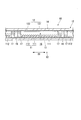
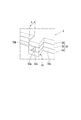
- FIG. 1 is a side view schematically showing a production apparatus for a dye-sensitized solar cell according to a first embodiment of the present invention.
- FIG. 2 is a cross-sectional view showing a schematic configuration of the dye-sensitized solar cell shown in FIG.
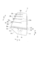
- FIG. 3 is a perspective view showing the overall configuration of the die coater shown in FIG.
- FIG. 4 is a perspective view showing a state in which the first shim piece is arranged in the first block in the die coater.
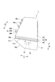
- FIG. 5 is a perspective view showing a state in which the second shim piece is arranged on the first shim piece in the die coater.
- FIG. 1 is a side view schematically showing a production apparatus for a dye-sensitized solar cell according to a first embodiment of the present invention.
- FIG. 2 is a cross-sectional view showing a schematic configuration of the dye-sensitized solar cell shown in FIG.
- FIG. 3 is a perspective view showing the overall configuration
- FIG. 6 is a perspective view showing a state in which the third shim piece is arranged on the second shim piece in the die coater.
- FIG. 7 is an enlarged perspective view of the convex discharge portion of the shim as seen from the discharge port side.
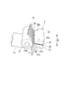
- FIG. 8 is a plan view showing a state in which the electrolytic solution is applied to the semiconductor electrode of the first base material by the die coater, and shows the state of the second shim piece.
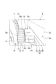
- FIG. 9 is an enlarged perspective view showing a coating state by the convex discharge portion of the die coater shown in FIG.
- FIG. 10 is a perspective view showing the overall configuration of the die coater according to the second embodiment.
- the die coater 3 of the present embodiment is provided in a manufacturing apparatus 1 for manufacturing a film-type dye-sensitized solar cell 10.
- the dye-sensitized solar cell 10 is electrically connected to the first base material 13, the second base material 14, the semiconductor electrode 11, the counter electrode 12, the electrolytic solution 15 (coating solution).
- the material 16 is provided.
- the semiconductor electrode 11 includes a transparent conductive film 111 stacked on the first base material 13 and a porous semiconductor layer 112 stacked on the transparent conductive film 111.
- the counter electrode 12 includes a counter conductive film 121 stacked on the second base material 14 and a catalyst layer 122 stacked on the counter conductive film 121. In order to obtain a series structure, an insulating portion is required, and therefore, an insulating treatment may be performed as necessary.
- Sealing materials 17 and 17 are arranged on both sides of the conductive material 16 of the dye-sensitized solar cell 10.
- the conductive material 16 and the sealing material 17 bond the electrodes (that is, between the semiconductor electrode 11 and the counter electrode 12).
- a sealing material is disposed or bonded by means such as ultrasonic fusion. In this way, the cells each having the semiconductor layer 112 are sealed in a liquid-tight manner.
- the conductive material 16 forms a gap in the thickness direction between the semiconductor electrode 11 and the counter electrode 12, and the electrolytic solution 15 is sealed in the gap.
- the transparent conductive film 111 and the counter conductive film 121 between adjacent cells are partitioned into a plurality by the patterning portion, and a pattern of the plurality of transparent conductive films 111 and the counter conductive film 121 is formed.
- the conductive film 121 electrically connects the counter conductive film 121 that forms the counter electrode 12 of one cell and the transparent conductive film 111 that forms the semiconductor electrode 11 of the other cell adjacent to the one cell. Connected.
- the material of the 1st base material 13 and the 2nd base material 14 is not specifically limited, For example, insulators, such as resin, a semiconductor, a metal, glass, etc. are mentioned.
- the resin include poly (meth) acrylic acid ester, polycarbonate, polyester, polyimide, polystyrene, polyvinyl chloride, and polyamide.
- the base material is preferably made of a transparent resin, more preferably a polyethylene terephthalate (PET) film or a polyethylene naphthalate (PEN) film. .
- the type and material of the transparent conductive film 111 and the counter conductive film 121 are not particularly limited, and a conductive film used for a known dye-sensitized solar cell is applicable.
- a thin film made of a metal oxide is used.
- the metal oxide include tin-doped indium oxide (ITO), fluorine-doped tin oxide (FTO), aluminum-doped zinc oxide (ATO), indium oxide / zinc oxide (IZO), and gallium-doped zinc oxide (GZO). it can.
- the semiconductor layer 112 is made of a material that can receive electrons from the adsorbed photosensitizing dye, and is usually preferably porous.
- the material forming the semiconductor layer 112 is not particularly limited, and a known material for the semiconductor layer 112 can be used. Examples thereof include metal oxide semiconductors such as titanium oxide, zinc oxide, and tin oxide.
- the photosensitizing dye supported on the semiconductor layer 112 is not particularly limited, and examples thereof include known dyes such as organic dyes and metal complex dyes. Examples of the organic dye include coumarin, polyene, cyanine, hemicyanine, and thiophene. As said metal complex pigment
- the electrolytic solution 15 is applied by the die coater 3 of the present embodiment, and examples thereof include an electrolytic solution in which iodine and sodium iodide are dissolved in an organic solvent and the viscosity is as small as that of water.
- an organic solvent such as acetonitrile, dimethylpropylimidazolium iodide or butylmethylimidazolium iodide, or a liquid component such as an ionic liquid was mixed with a supporting electrolyte such as lithium iodide and iodine.
- Examples include solutions.
- a known photosensitizing dye (not shown) is adsorbed on the surface of the semiconductor layer 112 in contact with the electrolytic solution 15 including the porous interior.
- the manufacturing apparatus 1 electrolyzes a semiconductor electrode forming portion (not shown) for forming the semiconductor electrode 11 in a predetermined region on the surface of the first base material 13 and the semiconductor electrode 11 formed at least in the predetermined region of the first base material 13.
- An electrolytic solution application part (die coater 3) for applying the liquid 15 and a downstream side in the transport direction P1 from the die coater 3 are sealed in an uncoated region of the electrolytic solution 15 in the first substrate 13
- the base material laminating portion 6 (6A, 6B) for pasting the second base material 14 on which the layer 122 (see FIG. 2) is formed to the first base material 13 and the base material laminating portion 6
- the heating unit 7 that fixes the adhesion between the first base material 13 and the second base material 14, and the first base material 13 and the second base material 14 Insulated section for performing insulation treatment in place of the cell sheets that are bonded together comprising a (not shown), and a.
- a semiconductor electrode 11 is formed at the most upstream portion in the transport direction P1, and a roll portion 10A that is wound in advance in a roll shape with the surface of the first base material 13 facing outward in the radial direction is installed.
- a first transport roll 21 for raising and transporting the first base material 13 obliquely upward is disposed near the downstream of the transport direction P1 extending substantially horizontally from the installation position of the roll unit 10A.
- the die coater 3 installed in a horizontal posture with the discharge port 33 a facing sideways is disposed.
- the discharge port 33 a of the die coater 3 is directed to a position where the electrolytic solution 15 can be applied to the semiconductor electrode 11 of the first base material 13 wound around the first transport roll 21.
- the second base material 13 is transported continuously along the transport direction P1 and the second base material 13 is formed with the semiconductor electrode 11 in a predetermined region on the surface.
- the dye-sensitized solar cell 10 is manufactured by bonding the base material 14 together.
- the method of manufacturing the dye-sensitized solar cell 10 at this time is as follows.
- the electrolytic solution coating step of applying the electrolytic solution 15 to the semiconductor electrode 11 of the first substrate 13 in the die coater 3, and the electrolytic solution coating step After the encapsulant coating process for applying the encapsulant 17 to the uncoated area of the electrolyte solution 15 on the surface of the first base material 13 in the encapsulant coating part 4, and the encapsulant coating process, After the wiring forming step of forming a wiring (conducting material 16) between the sealing materials 17 in the wiring forming portion 5 and the wiring forming step, the catalyst layer 122 is formed on the surface in the substrate bonding portion 6. And a base material laminating step for laminating the second base material 14 to the first base material 13.
- the dye-sensitized solar cell 10 is manufactured by such a manufacturing method.
- the die coater 3 includes a first block 31 having a liquid chamber 3 a (see FIG. 4) in which the electrolytic solution 15 is accommodated, and a second block 32 disposed to face the first block 31. And a convex discharge portion 33 that is sandwiched between the first block 31 and the second block 32 and protrudes from a part in the width direction W toward the discharge and discharges the electrolytic solution 15 in the liquid chamber 3a. And a shim 30.
- the first block 31, the second block 32, and the shim 30 correspond to the discharge main body of the present invention.
- the first block 31, the shim 30, and the second block 32 are stacked, and the stacking direction is referred to as a thickness direction H.
- a direction orthogonal to the thickness direction H when viewed from the direction along the width direction W is referred to as a front-rear direction E.
- the width dimension of the die coater 3 is substantially equal to the width dimension of the dye-sensitized solar cell 10.
- the width dimension of the die coater 3 is set such that a plurality of convex discharge portions 33 can be arranged so that the electrolytic solution 15 can be applied to the semiconductor electrode 11 formed in a predetermined region on the surface of the first base material 13. It only has to be.
- the upper surface 31a near the shim 30 in the thickness direction H forms a flat surface
- the first block 31 has a concave groove shape extending in the width direction W at a substantially central position in the front-rear direction E of the upper surface 31a.
- the liquid chamber 3a is formed.
- the liquid chamber 3a is provided with a supply hole 3b through which the electrolytic solution 15 is supplied by a pump (not shown) or the like.
- the lower surface 32a near the shim 30 in the thickness direction H is a flat surface.
- the upper surface 31a of the first block 31 and the lower surface 32a of the second block 32 face each other with the plate-like shim 30 sandwiched therebetween.
- the first block 31 and the second block 32 are detachably fixed by fixing means such as bolts (not shown) with the shim 30 sandwiched therebetween.
- the front portions of the first block 31 and the second block 32 in the front-rear direction E are formed with inclined surfaces 31b and 32b that gradually approach the shim 30 in the thickness direction H as they go forward.
- the front end surfaces 31c and 32c (see FIG. 9) of the first block 31 and the second block 32 are substantially coincident with each other in the front-rear direction.
- the shim 30 is formed with a discharge flow path (a slit 35 a to be described later) that communicates the liquid chamber 3 a and the discharge port 33 a of the convex discharge portion 33.
- a discharge flow path a slit 35 a to be described later
- the shim 30 is stacked on the first block 31, and the first shim piece 34 having an opening 34a communicating with the liquid chamber 3a is formed on the first shim piece 34.
- the second shim piece 35 formed with a slit 35a (discharge flow path) that is stacked and communicated from the discharge port 33a to the opening 34a is sandwiched between the second shim piece 35 and the second block 32 (see FIG. 3).
- the first shim piece 34, the second shim piece 35, and the third shim piece 36 are each made of a metal foil, and are all formed in the same outer shape in a plan view as viewed from the thickness direction H.
- the width dimension of the protruding tip 33 b in the convex discharge portion 33 is determined by the coating of the semiconductor electrode 11 (coating portion) of the first base material 13 to which the electrolytic solution 15 is applied. It is set to 30% or more and 100% or less of the width dimension of the work area.
- the “coating region” refers to a region where the liquid (electrolytic solution 15) exists after the first base material 13 and the second base material 14 are bonded together, that is, when the production of the battery is completed. is there.
- the protrusion length L from the front end surface 30a of the convex discharge part 33 can be set to about 2 mm, for example, but it is preferable that it is 0.1 mm or more and 30 mm or less, and it is 0.5 mm or more and 10 mm or less. Is more preferable, and it is still more preferable that it is 0.8 mm or more and 5 mm or less.
- the first shim piece 34 is formed with an opening 34 a having substantially the same shape as the liquid chamber 3 a and a first convex portion 34 b constituting a part of the convex discharge portion 33.
- the second shim piece 35 includes a plurality of slits 35 a extending in the front-rear direction E from the discharge port 33 a to at least a position overlapping the opening 34 a of the first shim piece 34, and part of the convex discharge portion 33.
- 2nd convex part 35b which comprises.
- the third shim piece 36 is formed with a third convex portion 36 b that constitutes a part of the convex discharge portion 33.
- the surface roughness of the part in contact with the electrolytic solution 15 is low in the viscosity of the electrolytic solution 15 in the present embodiment, and the corrosiveness of the wetted part in contact with the electrolytic solution 15 is increased.
- the thickness Ra is preferably in the range of 0.025 to 1.6, and the maximum height roughness Rz is preferably in the range of 0.1 to 6.3.
- the surface roughness of the shim 30 is preferably about 0.8 to 1.6 in terms of arithmetic average roughness Ra. In particular, it is more preferable that the surface roughness of the important part (the aforementioned wetted part or the like) is finished with an arithmetic average roughness Ra of 0.1.
- Examples of geometrical tolerances of portions of the die coater 3 that are in contact with the electrolytic solution 15 are, for example, parallelism 0.003 mm, flatness 0.003 mm, straightness 0.003 mm, It is preferable to finish with a squareness of 0.01 mm.
- a polishing method by a melting process using an etching solution can be employed.
- a method by mirror polishing can be adopted.
- the shim 30 is disposed in a state where a gap S is opened between the convex discharge portion 33 and the first base material 13 of the dye-sensitized solar cell 10.
- the electrolytic solution 15 discharged from the discharge port 33a of the convex discharge portion 33 can be applied to a predetermined coating region of the first base material 13 by the surface tension generated in the gap S.
- the electrolytic solution 15 accommodated in the liquid chamber 3a in the die coater 3 is pushed out to a slit 35a formed in the shim 30 by a pump or the like, and further discharged from the discharge port 33a through the slit 35a. .
- the coating accuracy can be improved by setting the width dimension of the convex discharge part 33 according to the width dimension of the semiconductor electrode 11 of the first base material 13. For example, by applying the electrolytic solution 15 with the die coater 3 to the first base material 13 constituting the dye-sensitized solar cell 10 as in the present embodiment, the coating width and coating of the electrolytic solution 15 are applied.
- the film thickness can be provided with a desired accuracy.
- the shim 30 of the present embodiment has a configuration that can be easily divided together with the first block 31 and the second block 32, the shim 30 can be exchanged efficiently and in a short time. Then, for example, coating under different conditions can be performed only by replacing the shim with a different shape, quantity, etc. of the convex discharge section 33.
- a shim 30 including a slit 35a communicating with the liquid chamber 3a is configured by liquid-tightly laminating three of the first shim piece 34, the second shim piece 35, and the third shim piece 36. can do.
- the slit 35a of the second shim piece 35 is sandwiched and covered by the first shim piece 34 and the third shim piece 36 from both sides, the slit 35a is formed between the first block 31 and the second block 35.
- the electrolyte solution 15 is less likely to leak from the slit 35a.
- the concave portion is formed between the adjacent convex discharge portions 33 and 33, the surface tension generated between the adjacent convex discharge portions 33 and 33 and the first base material 13 is caused.
- the electrolyte solutions 15 are not in contact with each other, and the electrolyte solution 15 can be reliably applied to the first base material 13 at a predetermined interval in the width direction W.
- the coating accuracy can be improved by setting the width dimension of the convex discharge portion 33 according to the width dimension of the semiconductor electrode 11 of the first base material 13.
- the die coater 3A according to the second embodiment shown in FIG. 10 has a configuration in which only one second shim piece 35 is used among the shims 30 of the first embodiment described above. That is, the first shim piece 34 and the third shim piece 36 are omitted.
- the second shim piece 35 in this case is directly sandwiched between the first block 31 and the second block 32.
- the electrolytic solution 15 is discharged from the discharge port 33a of the convex discharge portion 33 by the power of the pump.
- the opening area of the convex discharge portion 33 by setting the 0.00015Mm 2 or 0.375 mm 2 or less, can be accurately discharged from the discharge port 33a regardless of the viscosity of the electrolyte 15. Therefore, the region where surface tension is generated in the discharged electrolyte solution 15 is the range of the width of the convex discharge portion 33, and the coating width and coating film thickness of the electrolyte solution 15 can be provided with desired accuracy. It becomes possible to raise more.
- the shim 30 has a configuration in which three shim pieces (a first shim piece 34, a second shim piece 35, and a third shim piece 36) are stacked, but the invention is not limited thereto.
- the convex discharge part 33 which protrudes toward the discharge direction from the front end surface 30a of the shim 30 is provided, and the discharge flow path which connects the discharge port 33a of the convex discharge part 33 and the liquid chamber 3a is provided.
- the plurality of shim pieces may not be stacked.
- the configuration related to the width dimension of the convex discharge portion 33, the quantity and position of the shim 30 in the width direction W, the protrusion amount L of the shim 30 from the tip surface 30a, etc. It is not limited to embodiment, It can set suitably according to the form of a to-be-coated part, and the conditions of a coating liquid. Further, the configuration of the first block 31 and the second block 32 is not limited to the configuration of the present embodiment, and can have an appropriate size and shape.
- the dye-sensitized solar cell 10 is targeted as a coating portion where the coating liquid is applied by the die coater 3, and the die coater 3 is applied to the roll-to-roll manufacturing apparatus 1.
- the present invention is not limited to such a coated part and a manufacturing apparatus.
- the shim pieces 34, 35, and 36 of the shim 30 are formed of metal foil.
- the member is not limited to the metal foil.
- the thickness of the shim is not limited to a thin plate such as a metal foil, and may be a resin member such as polytetrafluoroethylene or polypropylene (PP).
- the configuration of the die coater 3 is not limited to providing the shim 30.
- the shim member itself is omitted, and a hole is formed with a drilling tool such as a drill on plate-like members (discharge body) of various metals such as stainless steel, iron, aluminum, and titanium having a thickness of about 10 cm and various alloys.
- the thickness of the discharge main body is preferably 1 cm or more and 20 cm or less. By setting the thickness within such a range, deformation can be suppressed by the rigidity of the metal. When the thickness is smaller than the lower limit of 1 cm, a liquid chamber having a sufficient capacity cannot be provided, and the coating amount in the width direction is difficult to stabilize unless the aperture ratio of the convex discharge portion is adjusted. If the thickness exceeds the upper limit of 20 cm, the amount of metal increases and becomes heavier, so that the workability is poor and the cost is high.
- the dye-sensitized solar cell 10 is made into object as a battery manufactured with the manufacturing method using the die coater 3, it is not limited to the dye-sensitized solar cell 10, For example, secondary It can also be used for batteries such as batteries.
- the die coater, the dye-sensitized solar cell manufacturing apparatus, and the battery manufacturing method of the present invention even in the case of a low-viscosity coating liquid, coating can be performed accurately with a predetermined coating width and coating thickness. Can be crafted.
Landscapes
- Engineering & Computer Science (AREA)
- Power Engineering (AREA)
- Microelectronics & Electronic Packaging (AREA)
- Chemical & Material Sciences (AREA)
- Chemical Kinetics & Catalysis (AREA)
- Electrochemistry (AREA)
- Coating Apparatus (AREA)
- Hybrid Cells (AREA)
- Photovoltaic Devices (AREA)
Abstract
Description
本願は、2016年8月4日に日本に出願された特願2016-153700号に基づき優先権を主張し、その内容をここに援用する。
このような色素増感太陽電池の製造工程のうち例えば半導体電極と対電極との間に電解液(塗工液)を塗工する工程では、塗工装置の一つとして先端部に塗工液の吐出口となるスリットを有するダイコーターを採用するものが知られている。ダイコーターは、例えば特許文献2に記載されるように、内部に形成されたマニホールドへと塗工液を供給し、マニホールドからスリットへと塗工液を押し出し、スリットに近接させてフィルム状の基材を相対移動させることにより、基材の表面に対して表面張力を利用して塗工液を塗布するものである。そして、基材に塗工される塗工液の厚みを調整する場合には、ダイコーターと基材との間隔やダイコーターのスリット幅等を変更したり、マニホールドからスリットへの塗工液の押し出し量や押し出し速度を変えることで均一な厚みの塗工膜となるように調整することができる。
このようなダイコーターでは、基材の幅方向に沿って延びる吐出口と基材との間に所定の隙間を設けて、その隙間を利用して表面張力によって、吐出口に連通するスリットからを介して吐出される電解液を基材の表面に塗工している。
この場合には、電解液が基材における所定の塗工幅よりもはみ出して広い幅で塗工されるうえ、所定の塗工膜厚も確保できない虞がある。
(1)本発明の一態様に係るダイコーターは、基材の表面に塗工液を塗工する吐出本体を有するダイコーターであって、前記吐出本体は、塗工液が収容される液室と、前記塗工液が吐出される側の先端面から吐出方向に向けて突出するとともに、前記基材の幅方向に間隔をあけて設けられた複数の凸状吐出部と、該凸状吐出部の吐出口と前記液室とを連通する吐出流路と、を有し、前記凸状吐出部における突出先端の前記幅方向の寸法は、前記塗工液が塗工される前記基材における被塗工領域の幅寸法の30%以上100%以下であることを特徴としている。
このとき、吐出本体における塗工液が吐出される側の先端面から凸状吐出部が突出しているので、塗工液の粘性にかかわらず吐出口から吐出される塗工液に表面張力が生じる領域は凸状吐出部の幅寸法の範囲となる。つまり、塗工液の塗工量を増やす場合であっても、表面張力が作用する領域が吐出本体の先端面の幅方向全体にわたって広がることがなく、塗工幅すなわち塗工領域を一定に保つことができる。そして、凸状吐出部の幅寸法を塗工液が塗工される基材における被塗工領域の幅寸法の30%以上100%以下となっているので、塗工精度を向上させることができる。例えば、被塗工部が色素増感太陽電池を構成する基材に対して、本発明のダイコーターで塗工液として電解液を塗工することで、電解液の塗工幅及び塗工膜厚を所望の精度で設けることができる。
吐出本体を1cm以上20cm以下の厚さの範囲とすることで、金属の剛性により、変形を抑えることができる。とくに、下限値の1cmよりも厚みが小さい場合には、十分な容量の液室を設けることができず、凸状吐出部の開口率を調整しないと幅方向の塗工量が安定しにくくなる。厚みが上限値の20cmを超える場合には、金属の量が増えて重くなり、作業性が悪く、かつ高価になるという欠点がある。
この場合には、凸状吐出部の突出長が0.1mmよりも小さい場合には表面張力を凸状吐出部だけに集中させることが困難となり、30mmを超える場合には高粘性時に圧損が立ち易くなることから、0.1mm以上30mm以下の範囲とすることが好ましい。
このとき、シムにおける塗工液が吐出される側の先端面から凸状吐出部が突出しているので、吐出口から吐出される塗工液に表面張力が生じる領域はシムの凸状吐出部の幅寸法の範囲となり、表面張力が作用する領域がシムの先端面の幅方向全体にわたって広がることがなく、塗工幅すなわち塗工領域を一定に保つことができる。
本発明では、凸状吐出部が幅方向に間隔をあけて複数が設けられ、隣り合う凸状吐出部同士の間に凹部が形成されているので、隣り合う凸状吐出部と基材との間に生じる表面張力による塗工液同士が接することがなく、基材に対して幅方向に所定の間隔をあけて確実に塗工液を塗工することができる。
図1に示すように、本実施の形態のダイコーター3は、フィルム型の色素増感太陽電池10を製造するための製造装置1に設けられている。
半導体電極11は、第1基材13上に積層された透明導電膜111と、透明導電膜111上に積層された多孔質の半導体層112と、を備えている。
対向電極12は、第2基材14上に積層された対向導電膜121と、対向導電膜121上に積層された触媒層122と、を備えている。
直列構造にするためには、絶縁部分が必要なので、適宜必要に応じて絶縁処理を施してもよい。
導通材16と封止材17とにより、電極間(即ち、半導体電極11と対向電極12との間)を接着している。一方、導通材16の延在方向X1に交差する方向(電池幅方向X2)には、封止材を配すか、又は超音波融着等の手段により接着されている。このようにして、それぞれに半導体層112を有するセルが液密に封止されている。そして、導通材16によって、半導体電極11と対向電極12の間には厚み方向に間隙が形成され、その間隙内に電解液15が封止されている。
区画された各セルにおいて、一方のセルの対向電極12を構成する対向導電膜121と、一方のセルに隣接する他方のセルの半導体電極11を構成する透明導電膜111とが導通材16によって電気的に接続されている。
半導体層112に担持される光増感色素は特に限定されず、例えば有機色素、金属錯体色素等の公知の色素が挙げられる。前述の有機色素としては、例えば、クマリン系、ポリエン系、シアニン系、ヘミシアニン系、チオフェン系等が挙げられる。前記金属錯体色素としては、例えば、ルテニウム錯体等が好適に用いられる。
電解液15としては、例えば、アセトニトリル、ヨウ化ジメチルプロピルイミダゾリウム又はヨウ化ブチルメチルイミダゾリウム等の有機溶媒またはイオン液体などの液体成分に、ヨウ化リチウム等の支持電解質とヨウ素とが混合された溶液等が挙げられる。
電解液15が接触する半導体層112において多孔質内部を含む表面には、図示しない公知の光増感色素が吸着している。
製造装置1は、第1基材13の表面の所定領域に半導体電極11を形成する半導体電極形成部(図示略)と、少なくとも第1基材13の所定領域に形成された半導体電極11に電解液15を塗工する電解液塗工部(ダイコーター3)と、ダイコーター3よりも搬送方向P1の下流寄りに設けられ、第1基材13における電解液15の未塗工領域に封止材17(図2参照)を塗工する封止材塗工部4と、封止材17同士の間に配線(図2に示す導通材16)を形成する配線形成部5と、表面に触媒層122(図2参照)が形成された第2基材14を第1基材13に貼り合わせる基材貼合せ部6(6A、6B)と、基材貼合せ部6によって貼り合された第1基材13と第2基材14との接着を固定する加熱部7と、第1基材13及び第2基材14が貼り合されてなる電池シートの所定の位置に絶縁処理を施す絶縁処理部(図示略)と、を備えている。
図3に示すように、ダイコーター3は、電解液15が収容される液室3a(図4参照)を有する第1ブロック31と、第1ブロック31に対向して配置される第2ブロック32と、第1ブロック31および第2ブロック32の間に挟持されるとともに、幅方向Wの一部から吐出寄りに向けて突出し液室3a内の電解液15を吐出する凸状吐出部33を有するシム30と、を備えている。ここで、第1ブロック31、第2ブロック32、及びシム30は、本願発明の吐出本体に相当する。
ダイコーター3の幅寸法は、第1基材13の表面の所定領域に形成された半導体電極11に電解液15を塗工できるように複数の凸状吐出部33が配置可能な寸法に設定されていればよい。
第1ブロック31及び第2ブロック32の前後方向Eの前部は、それぞれ前方に向かうに従い漸次、厚み方向Hでシム30寄りとなる傾斜面31b、32bが形成されている。第1ブロック31及び第2ブロック32の先端面31c、32c(図9参照)は、それぞれ前後方向の位置がほぼ一致している。
図4~図7に示すように、具体的にシム30は、第1ブロック31に積層され、液室3aに連通する開口34aが形成された第1シム片34と、第1シム片34に積層され吐出口33aから開口34aに連通するスリット35a(吐出流路)が形成された第2シム片35と、第2シム片35と第2ブロック32(図3参照)との間に挟持され、スリット35aを第1シム片34と反対側から覆う第3シム片36と、を備えている。
第1シム片34、第2シム片35、及び第3シム片36は、それぞれ金属箔からなり、厚み方向Hから見た平面視ですべて同じ外形で形成されている。
図7及び図8に示すように、凸状吐出部33における突出先端33bの幅寸法は、電解液15が塗工される第1基材13の半導体電極11(被塗工部)の被塗工領域の幅寸法の30%以上100%以下に設定されている。ここで、「被塗工領域」とは、第1基材13と第2基材14とを貼り合わせた後、すなわち電池の作製が完了したときに液体(電解液15)が存在する領域である。
そして、凸状吐出部33の先端面30aからの突出長Lは、例えば2mm程度に設定することができるが、0.1mm以上30mm以下であることが好ましく、0.5mm以上10mm以下であることがより好ましく、0.8mm以上5mm以下であることがさらに好ましい。
第2シム片35は、図5に示すように、少なくとも第1シム片34の開口34aに重なる位置まで吐出口33aから前後方向Eに延びる複数のスリット35aと、凸状吐出部33の一部を構成する第2凸部35bと、が形成されている。
第3シム片36は、図6に示すように、凸状吐出部33の一部を構成する第3凸部36bが形成されている。
シム30の場合には、例えばエッチング液を使用することによる溶融処理による研磨方法を採用することができる。シム30以外のダイコーター3の部分は、鏡面研磨による方法を採用することができる。
本実施の形態では、図8及び図9に示すように、凸状吐出部33と色素増感太陽電池10の第1基材13との間に隙間Sをあけた状態でシム30を配置することで、凸状吐出部33の吐出口33aから吐出される電解液15を前記隙間Sに生じる表面張力によって第1基材13の所定の塗工領域に塗布することができる。図5に示すように、ダイコーター3内の液室3aに収容された電解液15は、ポンプ等によってシム30に形成されるスリット35aに押し出され、さらにスリット35aを通じて吐出口33aから吐出される。
このように、凸状吐出部33の幅寸法を第1基材13の半導体電極11の幅寸法に合わせて設定することで、塗工精度を向上させることができる。例えば本実施の形態のように色素増感太陽電池10を構成する第1基材13に対して、ダイコーター3で電解液15を塗工することで、電解液15の塗工幅及び塗工膜厚を所望の精度で設けることができる。
本実施の形態では、凸状吐出部33の幅寸法を第1基材13の半導体電極11の幅寸法に合わせて設定することで、塗工精度を向上させることができる。
図10に示す第2の実施の形態によるダイコーター3Aは、上述した第1の実施の形態のシム30のうち第2シム片35の1枚のみを使用した構成となっている。すなわち、第1シム片34と第3シム片36とが省略されている。この場合の第2シム片35は、第1ブロック31と第2ブロック32との間に直接、挟持されている。
第2の実施の形態によるダイコーター3Aでは、ポンプの動力によって凸状吐出部33の吐出口33aから電解液15が吐出される。
このとき、吐出口33aとスリット35aとの間に表面張力が生じることにより、先ず前後方向Eに電解液15を吐出することを助長し、吐出された電解液15が第1基材13に達する前に厚さ方向Hに液垂れすることを防ぐことができる。
本実施の形態では、ダイコーター3の構成として、シム30を設けることに限定されることはない。
例えば、シムの部材自体を省略し、厚みが10cm程度のステンレス、鉄、アルミ、チタンなどの各種金属や、各種の合金等の板状部材(吐出本体)にドリル等の穿孔具で穴を形成した後で、複数の凸状吐出部を加工するようにして製造された構成であっても良い。
吐出本体の厚さとしては、1cm以上20cm以下であることが好ましく、このような厚さの範囲とすることで、金属の剛性により、変形を抑えることができる。下限値の1cmよりも厚みが小さい場合には、十分な容量の液室を設けることができず、凸状吐出部の開口率を調整しないと幅方向の塗工量が安定しにくくなる。厚みが上限値の20cmを超える場合には、金属の量が増えて重くなり、作業性が悪く、かつ高価になるという欠点がある。
3、3A ダイコーター
3a 液室
10 色素増感太陽電池
11 半導体電極
12 対向電極
13 第1基材
14 第2基材
15 電解液(塗工液)
16 導通材
17 封止材
30 シム
30a 先端面
31 第1ブロック
32 第2ブロック
33 凸状吐出部
33a 吐出口
33b 突出先端
34 第1シム片
34a 開口
35 第2シム片
35a スリット
36 第3シム片
E 前後方向
H 厚さ方向
P1 搬送方向
W 幅方向
Claims (9)
- 基材の表面に塗工液を塗工する吐出本体を有するダイコーターであって、
前記吐出本体は、
塗工液が収容される液室と、
前記塗工液が吐出される側の先端面から吐出方向に向けて突出するとともに、前記基材の幅方向に間隔をあけて設けられた複数の凸状吐出部と、
該凸状吐出部の吐出口と前記液室とを連通する吐出流路と、を有し、
前記凸状吐出部における突出先端の前記幅方向の寸法は、前記塗工液が塗工される前記基材における被塗工領域の幅寸法の30%以上100%以下であることを特徴とする、ダイコーター。 - 前記吐出本体の厚さは、1cm以上20cm以下であることを特徴とする、請求項1に記載のダイコーター。
- 前記凸状吐出部の突出長は、0.1mm以上30mm以下であることを特徴とする、請求項1又は2に記載のダイコーター。
- 前記凸状吐出部の開口面積は、0.00015mm2以上0.375mm2以下であることを特徴とする、請求項1乃至3のいずれか1項に記載のダイコーター。
- 前記塗工液に接する部位の表面粗さは、算術平均粗さRaが0.025~1.6であり、かつ最大高さ粗さRzが0.1~6.3であることを特徴とする、請求項1乃至4のいずれか1項に記載のダイコーター。
- 前記吐出本体は、
前記液室を有する第1ブロックと、
前記第1ブロックに対向して配置される第2ブロックと、
前記第1ブロックおよび前記第2ブロックの間に挟持されるとともに、前記幅方向の一部から前記吐出方向に向けて突出し前記液室内の前記塗工液を吐出する前記凸状吐出部を有し、かつ前記吐出流路が形成されたシムと、
を備えていることを特徴とする、請求項1乃至5のいずれか1項に記載のダイコーター。 - 前記シムは、
前記第1ブロックに積層され、前記液室に連通する開口が形成された第1シム片と、
前記第1シム片に積層され、前記吐出口から前記開口に連通するスリット状の前記吐出流路が形成された第2シム片と、
前記第2シム片と前記第2ブロックとの間に挟持され、前記吐出流路を前記第1シム片と反対側から覆う第3シム片と、
を備えていることを特徴とする、請求項6に記載のダイコーター。 - 請求項1乃至7のいずれか1項に記載のダイコーターを使用し、所定方向に沿って連続的に搬送され表面の所定領域に半導体電極が形成された第1基材に対して第2基材を貼り合せることにより色素増感太陽電池を製造するための色素増感太陽電池の製造装置であって、
前記ダイコーターは、前記凸状吐出部が前記第1基材の前記半導体電極との間に隙間が形成されるように配置され、
前記凸状吐出部の吐出口から吐出される塗工液は前記隙間によって作用する表面張力によって前記第1基材の前記半導体電極に塗工されることを特徴とする、色素増感太陽電池の製造装置。 - 請求項1乃至7のいずれか1項に記載のダイコーターを使用して所定方向に沿って連続的に搬送され表面の所定領域に第1基材に対して第2基材を貼り合せることにより電池を製造するための電池の製造方法であって、
前記凸状吐出部が前記第1基材との間に隙間が形成されるように前記ダイコーターを配置する工程と、
前記凸状吐出部の吐出口から吐出される塗工液を、前記隙間によって作用する表面張力によって前記第1基材に塗工する工程と、
を有することを特徴とする、電池の製造方法。
Priority Applications (3)
| Application Number | Priority Date | Filing Date | Title |
|---|---|---|---|
| CN201780042191.XA CN109414720A (zh) | 2016-08-04 | 2017-08-03 | 模头涂布机、染料敏化太阳能电池的制造装置、及电池的制造方法 |
| JP2018531977A JPWO2018025960A1 (ja) | 2016-08-04 | 2017-08-03 | ダイコーター、色素増感太陽電池の製造装置、及び電池の製造方法 |
| KR1020197000393A KR20190034523A (ko) | 2016-08-04 | 2017-08-03 | 다이 코터, 색소 증감 태양 전지의 제조 장치, 및 전지의 제조 방법 |
Applications Claiming Priority (2)
| Application Number | Priority Date | Filing Date | Title |
|---|---|---|---|
| JP2016-153700 | 2016-08-04 | ||
| JP2016153700 | 2016-08-04 |
Publications (1)
| Publication Number | Publication Date |
|---|---|
| WO2018025960A1 true WO2018025960A1 (ja) | 2018-02-08 |
Family
ID=61072985
Family Applications (1)
| Application Number | Title | Priority Date | Filing Date |
|---|---|---|---|
| PCT/JP2017/028246 Ceased WO2018025960A1 (ja) | 2016-08-04 | 2017-08-03 | ダイコーター、色素増感太陽電池の製造装置、及び電池の製造方法 |
Country Status (5)
| Country | Link |
|---|---|
| JP (1) | JPWO2018025960A1 (ja) |
| KR (1) | KR20190034523A (ja) |
| CN (1) | CN109414720A (ja) |
| TW (1) | TW201808461A (ja) |
| WO (1) | WO2018025960A1 (ja) |
Cited By (5)
| Publication number | Priority date | Publication date | Assignee | Title |
|---|---|---|---|---|
| JP2022169850A (ja) * | 2021-04-28 | 2022-11-10 | 株式会社タンガロイ | ダイヘッド |
| JPWO2023157609A1 (ja) * | 2022-02-15 | 2023-08-24 | ||
| JP7455259B1 (ja) | 2023-06-13 | 2024-03-25 | 株式会社オリジン | 塗布装置及び塗布物質塗布済対象物の製造方法 |
| WO2025244408A1 (ko) * | 2024-05-24 | 2025-11-27 | 주식회사 엘지에너지솔루션 | 코팅 장치 및 이를 포함하는 전극 제조 장치 |
| WO2025258915A1 (ko) * | 2024-06-11 | 2025-12-18 | 주식회사 엘지에너지솔루션 | 코팅 장치 |
Families Citing this family (3)
| Publication number | Priority date | Publication date | Assignee | Title |
|---|---|---|---|---|
| CN113071157A (zh) * | 2021-04-28 | 2021-07-06 | 璞璘科技(杭州)有限公司 | 狭缝涂布式模板、制作该模板的涂布头、设备及方法 |
| KR102656809B1 (ko) * | 2022-04-05 | 2024-04-12 | 주식회사 엘지에너지솔루션 | 활물질의 다층 코팅이 가능한 다이 코터 |
| CN119702336B (zh) * | 2023-09-28 | 2025-11-11 | 芯体素(杭州)科技发展有限公司 | 一种用于制备微结构电池极片的狭缝式涂布模头 |
Citations (4)
| Publication number | Priority date | Publication date | Assignee | Title |
|---|---|---|---|---|
| JP2013127923A (ja) * | 2011-12-19 | 2013-06-27 | Dainippon Printing Co Ltd | 色素増感型太陽電池素子、色素増感型太陽電池モジュール、色素増感型太陽電池素子の製造方法および酸化物半導体電極基板 |
| JP2013215716A (ja) * | 2012-03-16 | 2013-10-24 | Toray Ind Inc | ノズルの清掃装置および清掃方法並びにディスプレイ用部材の製造方法 |
| JP2015192992A (ja) * | 2014-03-20 | 2015-11-05 | 東レ株式会社 | ノズル及び塗液の排出方法 |
| JP2016078012A (ja) * | 2014-10-22 | 2016-05-16 | 東レ株式会社 | 塗布器 |
Family Cites Families (4)
| Publication number | Priority date | Publication date | Assignee | Title |
|---|---|---|---|---|
| US7591903B2 (en) * | 2002-08-13 | 2009-09-22 | 3M Innovative Properties Company | Die having multiple orifice slot |
| CN100587972C (zh) * | 2006-12-22 | 2010-02-03 | 索尼德国有限责任公司 | 光电池 |
| JP5007168B2 (ja) | 2007-07-10 | 2012-08-22 | 日東電工株式会社 | ダイコーター調整方法及び光学フィルムの製造方法 |
| JP2012174596A (ja) | 2011-02-23 | 2012-09-10 | Sony Corp | 色素増感太陽電池および色素増感太陽電池の製造方法、ならびに色素増感太陽電池モジュール |
-
2017
- 2017-08-03 KR KR1020197000393A patent/KR20190034523A/ko not_active Withdrawn
- 2017-08-03 TW TW106126230A patent/TW201808461A/zh unknown
- 2017-08-03 CN CN201780042191.XA patent/CN109414720A/zh active Pending
- 2017-08-03 WO PCT/JP2017/028246 patent/WO2018025960A1/ja not_active Ceased
- 2017-08-03 JP JP2018531977A patent/JPWO2018025960A1/ja active Pending
Patent Citations (4)
| Publication number | Priority date | Publication date | Assignee | Title |
|---|---|---|---|---|
| JP2013127923A (ja) * | 2011-12-19 | 2013-06-27 | Dainippon Printing Co Ltd | 色素増感型太陽電池素子、色素増感型太陽電池モジュール、色素増感型太陽電池素子の製造方法および酸化物半導体電極基板 |
| JP2013215716A (ja) * | 2012-03-16 | 2013-10-24 | Toray Ind Inc | ノズルの清掃装置および清掃方法並びにディスプレイ用部材の製造方法 |
| JP2015192992A (ja) * | 2014-03-20 | 2015-11-05 | 東レ株式会社 | ノズル及び塗液の排出方法 |
| JP2016078012A (ja) * | 2014-10-22 | 2016-05-16 | 東レ株式会社 | 塗布器 |
Cited By (8)
| Publication number | Priority date | Publication date | Assignee | Title |
|---|---|---|---|---|
| JP2022169850A (ja) * | 2021-04-28 | 2022-11-10 | 株式会社タンガロイ | ダイヘッド |
| JPWO2023157609A1 (ja) * | 2022-02-15 | 2023-08-24 | ||
| JP7538377B2 (ja) | 2022-02-15 | 2024-08-21 | 株式会社ヒラノテクシード | ダイ |
| JP7455259B1 (ja) | 2023-06-13 | 2024-03-25 | 株式会社オリジン | 塗布装置及び塗布物質塗布済対象物の製造方法 |
| WO2024257614A1 (ja) * | 2023-06-13 | 2024-12-19 | 株式会社オリジン | 塗布装置及び塗布物質塗布済対象物の製造方法 |
| JP2024178832A (ja) * | 2023-06-13 | 2024-12-25 | 株式会社オリジン | 塗布装置及び塗布物質塗布済対象物の製造方法 |
| WO2025244408A1 (ko) * | 2024-05-24 | 2025-11-27 | 주식회사 엘지에너지솔루션 | 코팅 장치 및 이를 포함하는 전극 제조 장치 |
| WO2025258915A1 (ko) * | 2024-06-11 | 2025-12-18 | 주식회사 엘지에너지솔루션 | 코팅 장치 |
Also Published As
| Publication number | Publication date |
|---|---|
| TW201808461A (zh) | 2018-03-16 |
| CN109414720A (zh) | 2019-03-01 |
| JPWO2018025960A1 (ja) | 2019-06-06 |
| KR20190034523A (ko) | 2019-04-02 |
Similar Documents
| Publication | Publication Date | Title |
|---|---|---|
| JPWO2018025960A1 (ja) | ダイコーター、色素増感太陽電池の製造装置、及び電池の製造方法 | |
| US10644273B2 (en) | Secondary battery metal terminal coating resin film, method for manufacturing same and battery pack | |
| CN215593226U (zh) | 一种电镀装置 | |
| JP2010511103A5 (ja) | ||
| US20240149292A1 (en) | Slot Die Coater And Multi-Lane Double Coating Device Including The Same | |
| EP3076227A1 (en) | Transmittance-variable film and method for producing same | |
| US9991058B2 (en) | Method for manufacturing solar cell | |
| JP6352268B2 (ja) | 光電変換素子の製造方法 | |
| JP6286110B2 (ja) | 電気モジュールの製造方法および電気モジュールの製造装置 | |
| CN105143522B (zh) | 连续镀敷装置 | |
| KR101833913B1 (ko) | 알루미늄 파우치 필름 제조용 슬롯 다이 코터 | |
| JP6918521B2 (ja) | 電気モジュールおよび電気モジュールの製造方法 | |
| JP6595894B2 (ja) | 粘性体供給装置、及び色素増感太陽電池の製造方法 | |
| KR101539959B1 (ko) | 유기 태양 전지 제조 방법 | |
| JP6680651B2 (ja) | 電気モジュールの製造方法及び電気モジュールの製造装置 | |
| JP6777477B2 (ja) | 電気モジュールの製造方法及び電気モジュールの製造装置 | |
| CN105513833A (zh) | 一种锂离子电容器电极的涂覆系统及其涂覆方法 | |
| JP2013194242A (ja) | 板状ワークの片面めっき装置 | |
| JP4779370B2 (ja) | 太陽電池及びその製造法 | |
| CN222008153U (zh) | 电镀阳极机构和电镀设备 | |
| JP6530686B2 (ja) | 電気モジュールの製造装置 | |
| JP6760885B2 (ja) | 電気モジュール及び電気モジュールの製造方法 | |
| JP2017108072A (ja) | 電気モジュールの製造装置及び電気モジュールの製造方法 | |
| US20220123024A1 (en) | Array substrate, method for preparing array substrate, and backlight module | |
| WO2019146684A1 (ja) | 電気モジュール及び電気モジュールの製造方法 |
Legal Events
| Date | Code | Title | Description |
|---|---|---|---|
| 121 | Ep: the epo has been informed by wipo that ep was designated in this application |
Ref document number: 17837061 Country of ref document: EP Kind code of ref document: A1 |
|
| ENP | Entry into the national phase |
Ref document number: 20197000393 Country of ref document: KR Kind code of ref document: A |
|
| ENP | Entry into the national phase |
Ref document number: 2018531977 Country of ref document: JP Kind code of ref document: A |
|
| NENP | Non-entry into the national phase |
Ref country code: DE |
|
| 122 | Ep: pct application non-entry in european phase |
Ref document number: 17837061 Country of ref document: EP Kind code of ref document: A1 |