WO2018021133A1 - 有機エレクトロニクス材料及びその利用 - Google Patents
有機エレクトロニクス材料及びその利用 Download PDFInfo
- Publication number
- WO2018021133A1 WO2018021133A1 PCT/JP2017/026222 JP2017026222W WO2018021133A1 WO 2018021133 A1 WO2018021133 A1 WO 2018021133A1 JP 2017026222 W JP2017026222 W JP 2017026222W WO 2018021133 A1 WO2018021133 A1 WO 2018021133A1
- Authority
- WO
- WIPO (PCT)
- Prior art keywords
- organic
- charge transporting
- group
- transporting polymer
- organic electronic
- Prior art date
Links
- 239000012776 electronic material Substances 0.000 title claims abstract description 68
- 229920000642 polymer Polymers 0.000 claims abstract description 173
- 125000000524 functional group Chemical group 0.000 claims abstract description 62
- 239000010410 layer Substances 0.000 claims description 61
- 239000012044 organic layer Substances 0.000 claims description 38
- 239000000463 material Substances 0.000 claims description 37
- 125000001997 phenyl group Chemical group [H]C1=C([H])C([H])=C(*)C([H])=C1[H] 0.000 claims description 22
- 125000003566 oxetanyl group Chemical group 0.000 claims description 16
- 239000003505 polymerization initiator Substances 0.000 claims description 16
- 239000000758 substrate Substances 0.000 claims description 15
- 150000004982 aromatic amines Chemical group 0.000 claims description 11
- 125000000391 vinyl group Chemical group [H]C([*])=C([H])[H] 0.000 claims description 11
- 125000000609 carbazolyl group Chemical group C1(=CC=CC=2C3=CC=CC=C3NC12)* 0.000 claims description 10
- YTPLMLYBLZKORZ-UHFFFAOYSA-N Thiophene Chemical group C=1C=CSC=1 YTPLMLYBLZKORZ-UHFFFAOYSA-N 0.000 claims description 8
- 125000003983 fluorenyl group Chemical group C1(=CC=CC=2C3=CC=CC=C3CC12)* 0.000 claims description 8
- 239000004973 liquid crystal related substance Substances 0.000 claims description 8
- 150000003839 salts Chemical class 0.000 claims description 8
- OHZAHWOAMVVGEL-UHFFFAOYSA-N 2,2'-bithiophene Chemical group C1=CSC(C=2SC=CC=2)=C1 OHZAHWOAMVVGEL-UHFFFAOYSA-N 0.000 claims description 6
- 238000010538 cationic polymerization reaction Methods 0.000 claims description 6
- 238000005401 electroluminescence Methods 0.000 claims description 6
- 229920005989 resin Polymers 0.000 claims description 6
- 239000011347 resin Substances 0.000 claims description 6
- 238000005286 illumination Methods 0.000 claims description 5
- 230000003111 delayed effect Effects 0.000 claims description 4
- -1 (substituted) oxetanyl Chemical group 0.000 abstract description 43
- 239000000178 monomer Substances 0.000 description 44
- 238000000034 method Methods 0.000 description 30
- 239000000203 mixture Substances 0.000 description 25
- YXFVVABEGXRONW-UHFFFAOYSA-N Toluene Chemical compound CC1=CC=CC=C1 YXFVVABEGXRONW-UHFFFAOYSA-N 0.000 description 21
- 238000002347 injection Methods 0.000 description 18
- 239000007924 injection Substances 0.000 description 18
- 239000002904 solvent Substances 0.000 description 18
- 239000002019 doping agent Substances 0.000 description 17
- OKKJLVBELUTLKV-UHFFFAOYSA-N Methanol Chemical compound OC OKKJLVBELUTLKV-UHFFFAOYSA-N 0.000 description 15
- 150000001875 compounds Chemical class 0.000 description 15
- 230000005525 hole transport Effects 0.000 description 15
- IJGRMHOSHXDMSA-UHFFFAOYSA-N Atomic nitrogen Chemical compound N#N IJGRMHOSHXDMSA-UHFFFAOYSA-N 0.000 description 14
- 125000004432 carbon atom Chemical group C* 0.000 description 14
- 239000010408 film Substances 0.000 description 14
- 125000004435 hydrogen atom Chemical group [H]* 0.000 description 13
- 125000001424 substituent group Chemical group 0.000 description 12
- WYURNTSHIVDZCO-UHFFFAOYSA-N Tetrahydrofuran Chemical compound C1CCOC1 WYURNTSHIVDZCO-UHFFFAOYSA-N 0.000 description 10
- RDOXTESZEPMUJZ-UHFFFAOYSA-N anisole Chemical compound COC1=CC=CC=C1 RDOXTESZEPMUJZ-UHFFFAOYSA-N 0.000 description 10
- 239000000126 substance Substances 0.000 description 10
- XEKOWRVHYACXOJ-UHFFFAOYSA-N Ethyl acetate Chemical compound CCOC(C)=O XEKOWRVHYACXOJ-UHFFFAOYSA-N 0.000 description 9
- 125000000217 alkyl group Chemical group 0.000 description 9
- 229910052757 nitrogen Inorganic materials 0.000 description 9
- 238000002360 preparation method Methods 0.000 description 9
- 150000004945 aromatic hydrocarbons Chemical class 0.000 description 8
- 125000003118 aryl group Chemical group 0.000 description 8
- 239000003054 catalyst Substances 0.000 description 8
- 238000000576 coating method Methods 0.000 description 8
- 238000004519 manufacturing process Methods 0.000 description 8
- 239000000243 solution Substances 0.000 description 8
- 230000000052 comparative effect Effects 0.000 description 7
- 238000005227 gel permeation chromatography Methods 0.000 description 7
- 238000007639 printing Methods 0.000 description 7
- 230000008569 process Effects 0.000 description 7
- YLQBMQCUIZJEEH-UHFFFAOYSA-N Furan Chemical group C=1C=COC=1 YLQBMQCUIZJEEH-UHFFFAOYSA-N 0.000 description 6
- UFWIBTONFRDIAS-UHFFFAOYSA-N Naphthalene Chemical compound C1=CC=CC2=CC=CC=C21 UFWIBTONFRDIAS-UHFFFAOYSA-N 0.000 description 6
- 239000000654 additive Substances 0.000 description 6
- ZADPBFCGQRWHPN-UHFFFAOYSA-N boronic acid Chemical compound OBO ZADPBFCGQRWHPN-UHFFFAOYSA-N 0.000 description 6
- 125000001246 bromo group Chemical group Br* 0.000 description 6
- 229920001577 copolymer Polymers 0.000 description 6
- 238000001914 filtration Methods 0.000 description 6
- 239000011521 glass Substances 0.000 description 6
- 150000008040 ionic compounds Chemical class 0.000 description 6
- KDLHZDBZIXYQEI-UHFFFAOYSA-N palladium Substances [Pd] KDLHZDBZIXYQEI-UHFFFAOYSA-N 0.000 description 6
- 239000002244 precipitate Substances 0.000 description 6
- 125000000732 arylene group Chemical group 0.000 description 5
- 230000015572 biosynthetic process Effects 0.000 description 5
- 230000008859 change Effects 0.000 description 5
- 125000004122 cyclic group Chemical group 0.000 description 5
- 125000001072 heteroaryl group Chemical group 0.000 description 5
- 238000005259 measurement Methods 0.000 description 5
- UZKWTJUDCOPSNM-UHFFFAOYSA-N methoxybenzene Substances CCCCOC=C UZKWTJUDCOPSNM-UHFFFAOYSA-N 0.000 description 5
- 238000007789 sealing Methods 0.000 description 5
- 238000001228 spectrum Methods 0.000 description 5
- VFUDMQLBKNMONU-UHFFFAOYSA-N 9-[4-(4-carbazol-9-ylphenyl)phenyl]carbazole Chemical compound C12=CC=CC=C2C2=CC=CC=C2N1C1=CC=C(C=2C=CC(=CC=2)N2C3=CC=CC=C3C3=CC=CC=C32)C=C1 VFUDMQLBKNMONU-UHFFFAOYSA-N 0.000 description 4
- 239000002841 Lewis acid Substances 0.000 description 4
- 239000002253 acid Substances 0.000 description 4
- MWPLVEDNUUSJAV-UHFFFAOYSA-N anthracene Chemical compound C1=CC=CC2=CC3=CC=CC=C3C=C21 MWPLVEDNUUSJAV-UHFFFAOYSA-N 0.000 description 4
- 230000000694 effects Effects 0.000 description 4
- UEEXRMUCXBPYOV-UHFFFAOYSA-N iridium;2-phenylpyridine Chemical compound [Ir].C1=CC=CC=C1C1=CC=CC=N1.C1=CC=CC=C1C1=CC=CC=N1.C1=CC=CC=C1C1=CC=CC=N1 UEEXRMUCXBPYOV-UHFFFAOYSA-N 0.000 description 4
- 150000007517 lewis acids Chemical class 0.000 description 4
- 239000007788 liquid Substances 0.000 description 4
- 239000002184 metal Chemical class 0.000 description 4
- 229910052751 metal Inorganic materials 0.000 description 4
- YNPNZTXNASCQKK-UHFFFAOYSA-N phenanthrene Chemical compound C1=CC=C2C3=CC=CC=C3C=CC2=C1 YNPNZTXNASCQKK-UHFFFAOYSA-N 0.000 description 4
- BASFCYQUMIYNBI-UHFFFAOYSA-N platinum Substances [Pt] BASFCYQUMIYNBI-UHFFFAOYSA-N 0.000 description 4
- BBEAQIROQSPTKN-UHFFFAOYSA-N pyrene Chemical compound C1=CC=C2C=CC3=CC=CC4=CC=C1C2=C43 BBEAQIROQSPTKN-UHFFFAOYSA-N 0.000 description 4
- 239000002516 radical scavenger Substances 0.000 description 4
- 239000007787 solid Substances 0.000 description 4
- RIOQSEWOXXDEQQ-UHFFFAOYSA-N triphenylphosphine Chemical compound C1=CC=CC=C1P(C=1C=CC=CC=1)C1=CC=CC=C1 RIOQSEWOXXDEQQ-UHFFFAOYSA-N 0.000 description 4
- XLYOFNOQVPJJNP-UHFFFAOYSA-N water Substances O XLYOFNOQVPJJNP-UHFFFAOYSA-N 0.000 description 4
- CYPYTURSJDMMMP-WVCUSYJESA-N (1e,4e)-1,5-diphenylpenta-1,4-dien-3-one;palladium Chemical compound [Pd].[Pd].C=1C=CC=CC=1\C=C\C(=O)\C=C\C1=CC=CC=C1.C=1C=CC=CC=1\C=C\C(=O)\C=C\C1=CC=CC=C1.C=1C=CC=CC=1\C=C\C(=O)\C=C\C1=CC=CC=C1 CYPYTURSJDMMMP-WVCUSYJESA-N 0.000 description 3
- CSCPPACGZOOCGX-UHFFFAOYSA-N Acetone Chemical compound CC(C)=O CSCPPACGZOOCGX-UHFFFAOYSA-N 0.000 description 3
- UHOVQNZJYSORNB-UHFFFAOYSA-N Benzene Chemical compound C1=CC=CC=C1 UHOVQNZJYSORNB-UHFFFAOYSA-N 0.000 description 3
- YMWUJEATGCHHMB-UHFFFAOYSA-N Dichloromethane Chemical compound ClCCl YMWUJEATGCHHMB-UHFFFAOYSA-N 0.000 description 3
- LFQSCWFLJHTTHZ-UHFFFAOYSA-N Ethanol Chemical compound CCO LFQSCWFLJHTTHZ-UHFFFAOYSA-N 0.000 description 3
- KFZMGEQAYNKOFK-UHFFFAOYSA-N Isopropanol Chemical compound CC(C)O KFZMGEQAYNKOFK-UHFFFAOYSA-N 0.000 description 3
- ZMXDDKWLCZADIW-UHFFFAOYSA-N N,N-Dimethylformamide Chemical compound CN(C)C=O ZMXDDKWLCZADIW-UHFFFAOYSA-N 0.000 description 3
- 239000004793 Polystyrene Substances 0.000 description 3
- VYPSYNLAJGMNEJ-UHFFFAOYSA-N Silicium dioxide Chemical compound O=[Si]=O VYPSYNLAJGMNEJ-UHFFFAOYSA-N 0.000 description 3
- 238000006069 Suzuki reaction reaction Methods 0.000 description 3
- 230000000996 additive effect Effects 0.000 description 3
- 125000006615 aromatic heterocyclic group Chemical group 0.000 description 3
- 238000006243 chemical reaction Methods 0.000 description 3
- 239000003086 colorant Substances 0.000 description 3
- 238000001723 curing Methods 0.000 description 3
- 125000003700 epoxy group Chemical group 0.000 description 3
- 239000003822 epoxy resin Substances 0.000 description 3
- 238000010438 heat treatment Methods 0.000 description 3
- 125000005549 heteroarylene group Chemical group 0.000 description 3
- 239000002346 layers by function Substances 0.000 description 3
- 125000005647 linker group Chemical group 0.000 description 3
- 229910052749 magnesium Inorganic materials 0.000 description 3
- 239000011159 matrix material Substances 0.000 description 3
- VLKZOEOYAKHREP-UHFFFAOYSA-N n-Hexane Chemical compound CCCCCC VLKZOEOYAKHREP-UHFFFAOYSA-N 0.000 description 3
- 125000001792 phenanthrenyl group Chemical group C1(=CC=CC=2C3=CC=CC=C3C=CC12)* 0.000 description 3
- 229920000647 polyepoxide Polymers 0.000 description 3
- 239000002861 polymer material Substances 0.000 description 3
- 229920002223 polystyrene Polymers 0.000 description 3
- 150000003384 small molecules Chemical class 0.000 description 3
- 239000003381 stabilizer Substances 0.000 description 3
- 230000002194 synthesizing effect Effects 0.000 description 3
- CXWXQJXEFPUFDZ-UHFFFAOYSA-N tetralin Chemical compound C1=CC=C2CCCCC2=C1 CXWXQJXEFPUFDZ-UHFFFAOYSA-N 0.000 description 3
- 238000007740 vapor deposition Methods 0.000 description 3
- DPZNOMCNRMUKPS-UHFFFAOYSA-N 1,3-Dimethoxybenzene Chemical compound COC1=CC=CC(OC)=C1 DPZNOMCNRMUKPS-UHFFFAOYSA-N 0.000 description 2
- CHLICZRVGGXEOD-UHFFFAOYSA-N 1-Methoxy-4-methylbenzene Chemical compound COC1=CC=C(C)C=C1 CHLICZRVGGXEOD-UHFFFAOYSA-N 0.000 description 2
- LTUJKAYZIMMJEP-UHFFFAOYSA-N 9-[4-(4-carbazol-9-yl-2-methylphenyl)-3-methylphenyl]carbazole Chemical compound C12=CC=CC=C2C2=CC=CC=C2N1C1=CC=C(C=2C(=CC(=CC=2)N2C3=CC=CC=C3C3=CC=CC=C32)C)C(C)=C1 LTUJKAYZIMMJEP-UHFFFAOYSA-N 0.000 description 2
- FMMWHPNWAFZXNH-UHFFFAOYSA-N Benz[a]pyrene Chemical compound C1=C2C3=CC=CC=C3C=C(C=C3)C2=C2C3=CC=CC2=C1 FMMWHPNWAFZXNH-UHFFFAOYSA-N 0.000 description 2
- HEDRZPFGACZZDS-UHFFFAOYSA-N Chloroform Chemical compound ClC(Cl)Cl HEDRZPFGACZZDS-UHFFFAOYSA-N 0.000 description 2
- LCGLNKUTAGEVQW-UHFFFAOYSA-N Dimethyl ether Chemical compound COC LCGLNKUTAGEVQW-UHFFFAOYSA-N 0.000 description 2
- IAZDPXIOMUYVGZ-UHFFFAOYSA-N Dimethylsulphoxide Chemical compound CS(C)=O IAZDPXIOMUYVGZ-UHFFFAOYSA-N 0.000 description 2
- AFVFQIVMOAPDHO-UHFFFAOYSA-N Methanesulfonic acid Chemical compound CS(O)(=O)=O AFVFQIVMOAPDHO-UHFFFAOYSA-N 0.000 description 2
- 238000005481 NMR spectroscopy Methods 0.000 description 2
- OFBQJSOFQDEBGM-UHFFFAOYSA-N Pentane Chemical compound CCCCC OFBQJSOFQDEBGM-UHFFFAOYSA-N 0.000 description 2
- XYFCBTPGUUZFHI-UHFFFAOYSA-N Phosphine Chemical compound P XYFCBTPGUUZFHI-UHFFFAOYSA-N 0.000 description 2
- 229920000265 Polyparaphenylene Polymers 0.000 description 2
- JUJWROOIHBZHMG-UHFFFAOYSA-N Pyridine Chemical group C1=CC=NC=C1 JUJWROOIHBZHMG-UHFFFAOYSA-N 0.000 description 2
- 229910052581 Si3N4 Inorganic materials 0.000 description 2
- DTQVDTLACAAQTR-UHFFFAOYSA-N Trifluoroacetic acid Chemical compound OC(=O)C(F)(F)F DTQVDTLACAAQTR-UHFFFAOYSA-N 0.000 description 2
- 125000003647 acryloyl group Chemical group O=C([*])C([H])=C([H])[H] 0.000 description 2
- 239000000853 adhesive Substances 0.000 description 2
- 230000001070 adhesive effect Effects 0.000 description 2
- 239000003513 alkali Substances 0.000 description 2
- 229910052783 alkali metal Inorganic materials 0.000 description 2
- 150000001340 alkali metals Chemical class 0.000 description 2
- 229910052784 alkaline earth metal Inorganic materials 0.000 description 2
- AZDRQVAHHNSJOQ-UHFFFAOYSA-N alumane Chemical class [AlH3] AZDRQVAHHNSJOQ-UHFFFAOYSA-N 0.000 description 2
- 150000001450 anions Chemical class 0.000 description 2
- 239000003963 antioxidant agent Substances 0.000 description 2
- 235000006708 antioxidants Nutrition 0.000 description 2
- 239000007864 aqueous solution Substances 0.000 description 2
- 150000008378 aryl ethers Chemical class 0.000 description 2
- 239000012298 atmosphere Substances 0.000 description 2
- UFVXQDWNSAGPHN-UHFFFAOYSA-K bis[(2-methylquinolin-8-yl)oxy]-(4-phenylphenoxy)alumane Chemical compound [Al+3].C1=CC=C([O-])C2=NC(C)=CC=C21.C1=CC=C([O-])C2=NC(C)=CC=C21.C1=CC([O-])=CC=C1C1=CC=CC=C1 UFVXQDWNSAGPHN-UHFFFAOYSA-K 0.000 description 2
- 230000000903 blocking effect Effects 0.000 description 2
- DKPFZGUDAPQIHT-UHFFFAOYSA-N butyl acetate Chemical compound CCCCOC(C)=O DKPFZGUDAPQIHT-UHFFFAOYSA-N 0.000 description 2
- XSIFPSYPOVKYCO-UHFFFAOYSA-N butyl benzoate Chemical compound CCCCOC(=O)C1=CC=CC=C1 XSIFPSYPOVKYCO-UHFFFAOYSA-N 0.000 description 2
- 229910052792 caesium Inorganic materials 0.000 description 2
- 229910052791 calcium Inorganic materials 0.000 description 2
- 229910052799 carbon Inorganic materials 0.000 description 2
- 229940125904 compound 1 Drugs 0.000 description 2
- 238000005859 coupling reaction Methods 0.000 description 2
- 239000000412 dendrimer Substances 0.000 description 2
- 229920000736 dendritic polymer Polymers 0.000 description 2
- 238000001514 detection method Methods 0.000 description 2
- 230000006866 deterioration Effects 0.000 description 2
- ZUOUZKKEUPVFJK-UHFFFAOYSA-N diphenyl Chemical group C1=CC=CC=C1C1=CC=CC=C1 ZUOUZKKEUPVFJK-UHFFFAOYSA-N 0.000 description 2
- 238000001035 drying Methods 0.000 description 2
- 239000003480 eluent Substances 0.000 description 2
- LZCLXQDLBQLTDK-UHFFFAOYSA-N ethyl 2-hydroxypropanoate Chemical compound CCOC(=O)C(C)O LZCLXQDLBQLTDK-UHFFFAOYSA-N 0.000 description 2
- MTZQAGJQAFMTAQ-UHFFFAOYSA-N ethyl benzoate Chemical compound CCOC(=O)C1=CC=CC=C1 MTZQAGJQAFMTAQ-UHFFFAOYSA-N 0.000 description 2
- LYCAIKOWRPUZTN-UHFFFAOYSA-N ethylene glycol Natural products OCCO LYCAIKOWRPUZTN-UHFFFAOYSA-N 0.000 description 2
- 230000002349 favourable effect Effects 0.000 description 2
- GVEPBJHOBDJJJI-UHFFFAOYSA-N fluoranthrene Natural products C1=CC(C2=CC=CC=C22)=C3C2=CC=CC3=C1 GVEPBJHOBDJJJI-UHFFFAOYSA-N 0.000 description 2
- 150000002366 halogen compounds Chemical class 0.000 description 2
- 125000005843 halogen group Chemical group 0.000 description 2
- 238000004128 high performance liquid chromatography Methods 0.000 description 2
- 229910052741 iridium Inorganic materials 0.000 description 2
- CECAIMUJVYQLKA-UHFFFAOYSA-N iridium 1-phenylisoquinoline Chemical compound [Ir].C1=CC=CC=C1C1=NC=CC2=CC=CC=C12.C1=CC=CC=C1C1=NC=CC2=CC=CC=C12.C1=CC=CC=C1C1=NC=CC2=CC=CC=C12 CECAIMUJVYQLKA-UHFFFAOYSA-N 0.000 description 2
- 239000005340 laminated glass Substances 0.000 description 2
- 238000007644 letterpress printing Methods 0.000 description 2
- 229910052744 lithium Inorganic materials 0.000 description 2
- GBMDVOWEEQVZKZ-UHFFFAOYSA-N methanol;hydrate Chemical compound O.OC GBMDVOWEEQVZKZ-UHFFFAOYSA-N 0.000 description 2
- QPJVMBTYPHYUOC-UHFFFAOYSA-N methyl benzoate Chemical compound COC(=O)C1=CC=CC=C1 QPJVMBTYPHYUOC-UHFFFAOYSA-N 0.000 description 2
- 238000002156 mixing Methods 0.000 description 2
- 238000007645 offset printing Methods 0.000 description 2
- 239000003960 organic solvent Substances 0.000 description 2
- 125000002080 perylenyl group Chemical group C1(=CC=C2C=CC=C3C4=CC=CC5=CC=CC(C1=C23)=C45)* 0.000 description 2
- CSHWQDPOILHKBI-UHFFFAOYSA-N peryrene Natural products C1=CC(C2=CC=CC=3C2=C2C=CC=3)=C3C2=CC=CC3=C1 CSHWQDPOILHKBI-UHFFFAOYSA-N 0.000 description 2
- 125000000843 phenylene group Chemical group C1(=C(C=CC=C1)*)* 0.000 description 2
- 238000000016 photochemical curing Methods 0.000 description 2
- 229910052697 platinum Inorganic materials 0.000 description 2
- 229920003227 poly(N-vinyl carbazole) Polymers 0.000 description 2
- 229920003207 poly(ethylene-2,6-naphthalate) Polymers 0.000 description 2
- 125000003367 polycyclic group Chemical group 0.000 description 2
- 239000011112 polyethylene naphthalate Substances 0.000 description 2
- 239000005020 polyethylene terephthalate Substances 0.000 description 2
- 229920000139 polyethylene terephthalate Polymers 0.000 description 2
- 229920002098 polyfluorene Polymers 0.000 description 2
- 238000006116 polymerization reaction Methods 0.000 description 2
- 229920001343 polytetrafluoroethylene Polymers 0.000 description 2
- 239000004810 polytetrafluoroethylene Substances 0.000 description 2
- 239000011148 porous material Substances 0.000 description 2
- 238000000746 purification Methods 0.000 description 2
- 125000000168 pyrrolyl group Chemical group 0.000 description 2
- 125000002943 quinolinyl group Chemical group N1=C(C=CC2=CC=CC=C12)* 0.000 description 2
- 125000001567 quinoxalinyl group Chemical group N1=C(C=NC2=CC=CC=C12)* 0.000 description 2
- 229920005604 random copolymer Polymers 0.000 description 2
- 239000012925 reference material Substances 0.000 description 2
- 238000010992 reflux Methods 0.000 description 2
- 239000005394 sealing glass Substances 0.000 description 2
- 238000004904 shortening Methods 0.000 description 2
- HQVNEWCFYHHQES-UHFFFAOYSA-N silicon nitride Chemical compound N12[Si]34N5[Si]62N3[Si]51N64 HQVNEWCFYHHQES-UHFFFAOYSA-N 0.000 description 2
- 229910052814 silicon oxide Inorganic materials 0.000 description 2
- 238000003756 stirring Methods 0.000 description 2
- 238000003786 synthesis reaction Methods 0.000 description 2
- NLDYACGHTUPAQU-UHFFFAOYSA-N tetracyanoethylene Chemical compound N#CC(C#N)=C(C#N)C#N NLDYACGHTUPAQU-UHFFFAOYSA-N 0.000 description 2
- PCCVSPMFGIFTHU-UHFFFAOYSA-N tetracyanoquinodimethane Chemical compound N#CC(C#N)=C1C=CC(=C(C#N)C#N)C=C1 PCCVSPMFGIFTHU-UHFFFAOYSA-N 0.000 description 2
- 229940073455 tetraethylammonium hydroxide Drugs 0.000 description 2
- LRGJRHZIDJQFCL-UHFFFAOYSA-M tetraethylazanium;hydroxide Chemical compound [OH-].CC[N+](CC)(CC)CC LRGJRHZIDJQFCL-UHFFFAOYSA-M 0.000 description 2
- JOXIMZWYDAKGHI-UHFFFAOYSA-N toluene-4-sulfonic acid Chemical compound CC1=CC=C(S(O)(=O)=O)C=C1 JOXIMZWYDAKGHI-UHFFFAOYSA-N 0.000 description 2
- 150000003623 transition metal compounds Chemical class 0.000 description 2
- ABDKAPXRBAPSQN-UHFFFAOYSA-N veratrole Chemical compound COC1=CC=CC=C1OC ABDKAPXRBAPSQN-UHFFFAOYSA-N 0.000 description 2
- MIOPJNTWMNEORI-GMSGAONNSA-N (S)-camphorsulfonic acid Chemical compound C1C[C@@]2(CS(O)(=O)=O)C(=O)C[C@@H]1C2(C)C MIOPJNTWMNEORI-GMSGAONNSA-N 0.000 description 1
- POILWHVDKZOXJZ-ARJAWSKDSA-M (z)-4-oxopent-2-en-2-olate Chemical compound C\C([O-])=C\C(C)=O POILWHVDKZOXJZ-ARJAWSKDSA-M 0.000 description 1
- FNQJDLTXOVEEFB-UHFFFAOYSA-N 1,2,3-benzothiadiazole Chemical group C1=CC=C2SN=NC2=C1 FNQJDLTXOVEEFB-UHFFFAOYSA-N 0.000 description 1
- SLLFVLKNXABYGI-UHFFFAOYSA-N 1,2,3-benzoxadiazole Chemical group C1=CC=C2ON=NC2=C1 SLLFVLKNXABYGI-UHFFFAOYSA-N 0.000 description 1
- UGUHFDPGDQDVGX-UHFFFAOYSA-N 1,2,3-thiadiazole Chemical group C1=CSN=N1 UGUHFDPGDQDVGX-UHFFFAOYSA-N 0.000 description 1
- LZDKZFUFMNSQCJ-UHFFFAOYSA-N 1,2-diethoxyethane Chemical compound CCOCCOCC LZDKZFUFMNSQCJ-UHFFFAOYSA-N 0.000 description 1
- YJTKZCDBKVTVBY-UHFFFAOYSA-N 1,3-Diphenylbenzene Chemical group C1=CC=CC=C1C1=CC=CC(C=2C=CC=CC=2)=C1 YJTKZCDBKVTVBY-UHFFFAOYSA-N 0.000 description 1
- 125000000355 1,3-benzoxazolyl group Chemical group O1C(=NC2=C1C=CC=C2)* 0.000 description 1
- OSIGJGFTADMDOB-UHFFFAOYSA-N 1-Methoxy-3-methylbenzene Chemical compound COC1=CC=CC(C)=C1 OSIGJGFTADMDOB-UHFFFAOYSA-N 0.000 description 1
- FCEHBMOGCRZNNI-UHFFFAOYSA-N 1-benzothiophene Chemical group C1=CC=C2SC=CC2=C1 FCEHBMOGCRZNNI-UHFFFAOYSA-N 0.000 description 1
- BLMBNEVGYRXFNA-UHFFFAOYSA-N 1-methoxy-2,3-dimethylbenzene Chemical compound COC1=CC=CC(C)=C1C BLMBNEVGYRXFNA-UHFFFAOYSA-N 0.000 description 1
- ARXJGSRGQADJSQ-UHFFFAOYSA-N 1-methoxypropan-2-ol Chemical compound COCC(C)O ARXJGSRGQADJSQ-UHFFFAOYSA-N 0.000 description 1
- MVWPVABZQQJTPL-UHFFFAOYSA-N 2,3-diphenylcyclohexa-2,5-diene-1,4-dione Chemical class O=C1C=CC(=O)C(C=2C=CC=CC=2)=C1C1=CC=CC=C1 MVWPVABZQQJTPL-UHFFFAOYSA-N 0.000 description 1
- UJCFZCTTZWHRNL-UHFFFAOYSA-N 2,4-Dimethylanisole Chemical compound COC1=CC=C(C)C=C1C UJCFZCTTZWHRNL-UHFFFAOYSA-N 0.000 description 1
- WBIQQQGBSDOWNP-UHFFFAOYSA-N 2-dodecylbenzenesulfonic acid Chemical compound CCCCCCCCCCCCC1=CC=CC=C1S(O)(=O)=O WBIQQQGBSDOWNP-UHFFFAOYSA-N 0.000 description 1
- DTFKRVXLBCAIOZ-UHFFFAOYSA-N 2-methylanisole Chemical compound COC1=CC=CC=C1C DTFKRVXLBCAIOZ-UHFFFAOYSA-N 0.000 description 1
- 125000003903 2-propenyl group Chemical group [H]C([*])([H])C([H])=C([H])[H] 0.000 description 1
- GOLORTLGFDVFDW-UHFFFAOYSA-N 3-(1h-benzimidazol-2-yl)-7-(diethylamino)chromen-2-one Chemical compound C1=CC=C2NC(C3=CC4=CC=C(C=C4OC3=O)N(CC)CC)=NC2=C1 GOLORTLGFDVFDW-UHFFFAOYSA-N 0.000 description 1
- MZYDBGLUVPLRKR-UHFFFAOYSA-N 9-(3-carbazol-9-ylphenyl)carbazole Chemical compound C12=CC=CC=C2C2=CC=CC=C2N1C1=CC(N2C3=CC=CC=C3C3=CC=CC=C32)=CC=C1 MZYDBGLUVPLRKR-UHFFFAOYSA-N 0.000 description 1
- ZYASLTYCYTYKFC-UHFFFAOYSA-N 9-methylidenefluorene Chemical class C1=CC=C2C(=C)C3=CC=CC=C3C2=C1 ZYASLTYCYTYKFC-UHFFFAOYSA-N 0.000 description 1
- QTBSBXVTEAMEQO-UHFFFAOYSA-M Acetate Chemical compound CC([O-])=O QTBSBXVTEAMEQO-UHFFFAOYSA-M 0.000 description 1
- 239000004925 Acrylic resin Substances 0.000 description 1
- 229920000178 Acrylic resin Polymers 0.000 description 1
- QGZKDVFQNNGYKY-UHFFFAOYSA-O Ammonium Chemical compound [NH4+] QGZKDVFQNNGYKY-UHFFFAOYSA-O 0.000 description 1
- 229910017008 AsF 6 Inorganic materials 0.000 description 1
- ROFVEXUMMXZLPA-UHFFFAOYSA-N Bipyridyl Chemical class N1=CC=CC=C1C1=CC=CC=N1 ROFVEXUMMXZLPA-UHFFFAOYSA-N 0.000 description 1
- BTBUEUYNUDRHOZ-UHFFFAOYSA-N Borate Chemical compound [O-]B([O-])[O-] BTBUEUYNUDRHOZ-UHFFFAOYSA-N 0.000 description 1
- 238000006443 Buchwald-Hartwig cross coupling reaction Methods 0.000 description 1
- QQTPMQLDWKPLFO-UHFFFAOYSA-N CCCCCCCCC1(C)c(cc(B2OC(C)(C)C(C)(C)O2)cc2)c2-c2ccc(B3OC(C)(C)C(C)(C)O3)cc12 Chemical compound CCCCCCCCC1(C)c(cc(B2OC(C)(C)C(C)(C)O2)cc2)c2-c2ccc(B3OC(C)(C)C(C)(C)O3)cc12 QQTPMQLDWKPLFO-UHFFFAOYSA-N 0.000 description 1
- RVRXBUSBHUXKRS-UHFFFAOYSA-N CCCCCc(cc1)ccc1-[n]1c2ccc(B3OC(C)(C)C(C)(C)O3)cc2c2cc(B3OC(C)(C)C(C)(C)O3)ccc12 Chemical compound CCCCCc(cc1)ccc1-[n]1c2ccc(B3OC(C)(C)C(C)(C)O3)cc2c2cc(B3OC(C)(C)C(C)(C)O3)ccc12 RVRXBUSBHUXKRS-UHFFFAOYSA-N 0.000 description 1
- SYWMSCIWMKWYKD-UHFFFAOYSA-N CCCCOc(cc1)ccc1N(c1ccc(B2OC(C)(C)C(C)(C)O2)cc1)c1ccc(B2OC(C)(C)C(C)(C)O2)cc1 Chemical compound CCCCOc(cc1)ccc1N(c1ccc(B2OC(C)(C)C(C)(C)O2)cc1)c1ccc(B2OC(C)(C)C(C)(C)O2)cc1 SYWMSCIWMKWYKD-UHFFFAOYSA-N 0.000 description 1
- MRMUIYADKDRHAA-UHFFFAOYSA-N CCCCc(cc1)ccc1N(c1ccc(B2OC(C)(C)C(C)(C)O2)cc1)c1ccc(B2OC(C)(C)C(C)(C)O2)cc1 Chemical compound CCCCc(cc1)ccc1N(c1ccc(B2OC(C)(C)C(C)(C)O2)cc1)c1ccc(B2OC(C)(C)C(C)(C)O2)cc1 MRMUIYADKDRHAA-UHFFFAOYSA-N 0.000 description 1
- 229920008347 Cellulose acetate propionate Polymers 0.000 description 1
- 229920002284 Cellulose triacetate Polymers 0.000 description 1
- XDTMQSROBMDMFD-UHFFFAOYSA-N Cyclohexane Chemical compound C1CCCCC1 XDTMQSROBMDMFD-UHFFFAOYSA-N 0.000 description 1
- AASWSXXTMLHQER-UHFFFAOYSA-N Fc(c([B](c(c(F)c(c(F)c1F)F)c1F)(c(c(F)c(c(F)c1F)F)c1F)c(c(F)c(c(F)c1F)F)c1F)c(c(F)c1F)F)c1F Chemical compound Fc(c([B](c(c(F)c(c(F)c1F)F)c1F)(c(c(F)c(c(F)c1F)F)c1F)c(c(F)c(c(F)c1F)F)c1F)c(c(F)c1F)F)c1F AASWSXXTMLHQER-UHFFFAOYSA-N 0.000 description 1
- 239000002879 Lewis base Substances 0.000 description 1
- FXHOOIRPVKKKFG-UHFFFAOYSA-N N,N-Dimethylacetamide Chemical compound CN(C)C(C)=O FXHOOIRPVKKKFG-UHFFFAOYSA-N 0.000 description 1
- 229910019800 NbF 5 Inorganic materials 0.000 description 1
- 238000006411 Negishi coupling reaction Methods 0.000 description 1
- CTQNGGLPUBDAKN-UHFFFAOYSA-N O-Xylene Chemical compound CC1=CC=CC=C1C CTQNGGLPUBDAKN-UHFFFAOYSA-N 0.000 description 1
- 229920000144 PEDOT:PSS Polymers 0.000 description 1
- 239000004696 Poly ether ether ketone Substances 0.000 description 1
- 239000004695 Polyether sulfone Substances 0.000 description 1
- 239000004697 Polyetherimide Substances 0.000 description 1
- 239000004642 Polyimide Substances 0.000 description 1
- 239000004734 Polyphenylene sulfide Substances 0.000 description 1
- 229910018287 SbF 5 Inorganic materials 0.000 description 1
- XUIMIQQOPSSXEZ-UHFFFAOYSA-N Silicon Chemical group [Si] XUIMIQQOPSSXEZ-UHFFFAOYSA-N 0.000 description 1
- 238000003477 Sonogashira cross-coupling reaction Methods 0.000 description 1
- PJANXHGTPQOBST-VAWYXSNFSA-N Stilbene Natural products C=1C=CC=CC=1/C=C/C1=CC=CC=C1 PJANXHGTPQOBST-VAWYXSNFSA-N 0.000 description 1
- 238000006619 Stille reaction Methods 0.000 description 1
- FZWLAAWBMGSTSO-UHFFFAOYSA-N Thiazole Chemical group C1=CSC=N1 FZWLAAWBMGSTSO-UHFFFAOYSA-N 0.000 description 1
- 239000007983 Tris buffer Substances 0.000 description 1
- 229910007926 ZrCl Inorganic materials 0.000 description 1
- NNLVGZFZQQXQNW-ADJNRHBOSA-N [(2r,3r,4s,5r,6s)-4,5-diacetyloxy-3-[(2s,3r,4s,5r,6r)-3,4,5-triacetyloxy-6-(acetyloxymethyl)oxan-2-yl]oxy-6-[(2r,3r,4s,5r,6s)-4,5,6-triacetyloxy-2-(acetyloxymethyl)oxan-3-yl]oxyoxan-2-yl]methyl acetate Chemical compound O([C@@H]1O[C@@H]([C@H]([C@H](OC(C)=O)[C@H]1OC(C)=O)O[C@H]1[C@@H]([C@@H](OC(C)=O)[C@H](OC(C)=O)[C@@H](COC(C)=O)O1)OC(C)=O)COC(=O)C)[C@@H]1[C@@H](COC(C)=O)O[C@@H](OC(C)=O)[C@H](OC(C)=O)[C@H]1OC(C)=O NNLVGZFZQQXQNW-ADJNRHBOSA-N 0.000 description 1
- IPBVNPXQWQGGJP-UHFFFAOYSA-N acetic acid phenyl ester Natural products CC(=O)OC1=CC=CC=C1 IPBVNPXQWQGGJP-UHFFFAOYSA-N 0.000 description 1
- CUJRVFIICFDLGR-UHFFFAOYSA-N acetylacetonate Chemical compound CC(=O)[CH-]C(C)=O CUJRVFIICFDLGR-UHFFFAOYSA-N 0.000 description 1
- 150000007513 acids Chemical class 0.000 description 1
- 125000000641 acridinyl group Chemical group C1(=CC=CC2=NC3=CC=CC=C3C=C12)* 0.000 description 1
- 150000001298 alcohols Chemical class 0.000 description 1
- 150000001335 aliphatic alkanes Chemical class 0.000 description 1
- 125000001931 aliphatic group Chemical group 0.000 description 1
- 150000001342 alkaline earth metals Chemical class 0.000 description 1
- 125000002947 alkylene group Chemical group 0.000 description 1
- 229920005603 alternating copolymer Polymers 0.000 description 1
- 229910052782 aluminium Inorganic materials 0.000 description 1
- 150000001408 amides Chemical class 0.000 description 1
- 238000010539 anionic addition polymerization reaction Methods 0.000 description 1
- 239000010405 anode material Substances 0.000 description 1
- 125000005577 anthracene group Chemical group 0.000 description 1
- 150000008425 anthrones Chemical class 0.000 description 1
- 239000002518 antifoaming agent Substances 0.000 description 1
- 229940058303 antinematodal benzimidazole derivative Drugs 0.000 description 1
- 125000004429 atom Chemical group 0.000 description 1
- QVGXLLKOCUKJST-UHFFFAOYSA-N atomic oxygen Chemical compound [O] QVGXLLKOCUKJST-UHFFFAOYSA-N 0.000 description 1
- 229910052788 barium Inorganic materials 0.000 description 1
- 239000002585 base Substances 0.000 description 1
- 150000001555 benzenes Chemical group 0.000 description 1
- SRSXLGNVWSONIS-UHFFFAOYSA-N benzenesulfonic acid Chemical compound OS(=O)(=O)C1=CC=CC=C1 SRSXLGNVWSONIS-UHFFFAOYSA-N 0.000 description 1
- 229940092714 benzenesulfonic acid Drugs 0.000 description 1
- 125000003785 benzimidazolyl group Chemical class N1=C(NC2=C1C=CC=C2)* 0.000 description 1
- FCEUOTOBJMBWHC-UHFFFAOYSA-N benzo[f]cinnoline Chemical group N1=CC=C2C3=CC=CC=C3C=CC2=N1 FCEUOTOBJMBWHC-UHFFFAOYSA-N 0.000 description 1
- UDEWPOVQBGFNGE-UHFFFAOYSA-N benzoic acid n-propyl ester Natural products CCCOC(=O)C1=CC=CC=C1 UDEWPOVQBGFNGE-UHFFFAOYSA-N 0.000 description 1
- IOJUPLGTWVMSFF-UHFFFAOYSA-N benzothiazole Chemical group C1=CC=C2SC=NC2=C1 IOJUPLGTWVMSFF-UHFFFAOYSA-N 0.000 description 1
- 125000003354 benzotriazolyl group Chemical group N1N=NC2=C1C=CC=C2* 0.000 description 1
- 239000004305 biphenyl Chemical group 0.000 description 1
- 235000010290 biphenyl Nutrition 0.000 description 1
- 229920001400 block copolymer Polymers 0.000 description 1
- 229940063013 borate ion Drugs 0.000 description 1
- QDHFHIQKOVNCNC-UHFFFAOYSA-N butane-1-sulfonic acid Chemical compound CCCCS(O)(=O)=O QDHFHIQKOVNCNC-UHFFFAOYSA-N 0.000 description 1
- 125000004369 butenyl group Chemical group C(=CCC)* 0.000 description 1
- 238000011088 calibration curve Methods 0.000 description 1
- 150000001718 carbodiimides Chemical class 0.000 description 1
- 150000001721 carbon Chemical group 0.000 description 1
- CREMABGTGYGIQB-UHFFFAOYSA-N carbon carbon Chemical compound C.C CREMABGTGYGIQB-UHFFFAOYSA-N 0.000 description 1
- 239000011203 carbon fibre reinforced carbon Substances 0.000 description 1
- 239000000969 carrier Substances 0.000 description 1
- 238000005266 casting Methods 0.000 description 1
- 239000010406 cathode material Substances 0.000 description 1
- 150000001768 cations Chemical class 0.000 description 1
- 239000003638 chemical reducing agent Substances 0.000 description 1
- 239000011248 coating agent Substances 0.000 description 1
- 239000011247 coating layer Substances 0.000 description 1
- 229920001940 conductive polymer Polymers 0.000 description 1
- 150000004696 coordination complex Chemical class 0.000 description 1
- 238000007334 copolymerization reaction Methods 0.000 description 1
- 238000006880 cross-coupling reaction Methods 0.000 description 1
- 125000006165 cyclic alkyl group Chemical group 0.000 description 1
- 150000004292 cyclic ethers Chemical group 0.000 description 1
- 150000001924 cycloalkanes Chemical class 0.000 description 1
- 125000001995 cyclobutyl group Chemical group [H]C1([H])C([H])([H])C([H])(*)C1([H])[H] 0.000 description 1
- 125000001559 cyclopropyl group Chemical group [H]C1([H])C([H])([H])C1([H])* 0.000 description 1
- 238000007872 degassing Methods 0.000 description 1
- 230000002542 deteriorative effect Effects 0.000 description 1
- 238000010586 diagram Methods 0.000 description 1
- XXPBFNVKTVJZKF-UHFFFAOYSA-N dihydrophenanthrene Chemical group C1=CC=C2CCC3=CC=CC=C3C2=C1 XXPBFNVKTVJZKF-UHFFFAOYSA-N 0.000 description 1
- WASQWSOJHCZDFK-UHFFFAOYSA-N diketene Chemical group C=C1CC(=O)O1 WASQWSOJHCZDFK-UHFFFAOYSA-N 0.000 description 1
- CZZYITDELCSZES-UHFFFAOYSA-N diphenylmethane Chemical compound C=1C=CC=CC=1CC1=CC=CC=C1 CZZYITDELCSZES-UHFFFAOYSA-N 0.000 description 1
- 238000007598 dipping method Methods 0.000 description 1
- 239000002270 dispersing agent Substances 0.000 description 1
- 229940060296 dodecylbenzenesulfonic acid Drugs 0.000 description 1
- 239000000975 dye Substances 0.000 description 1
- 239000003995 emulsifying agent Substances 0.000 description 1
- 230000002708 enhancing effect Effects 0.000 description 1
- 229940116333 ethyl lactate Drugs 0.000 description 1
- 125000002534 ethynyl group Chemical group [H]C#C* 0.000 description 1
- 239000003063 flame retardant Substances 0.000 description 1
- 150000002220 fluorenes Chemical group 0.000 description 1
- 239000007789 gas Substances 0.000 description 1
- 239000003349 gelling agent Substances 0.000 description 1
- 229920000578 graft copolymer Polymers 0.000 description 1
- 238000007646 gravure printing Methods 0.000 description 1
- 150000002390 heteroarenes Chemical class 0.000 description 1
- 125000000623 heterocyclic group Chemical group 0.000 description 1
- 238000004770 highest occupied molecular orbital Methods 0.000 description 1
- QWPPOHNGKGFGJK-UHFFFAOYSA-N hypochlorous acid Chemical compound ClO QWPPOHNGKGFGJK-UHFFFAOYSA-N 0.000 description 1
- 229910052738 indium Inorganic materials 0.000 description 1
- 229910003437 indium oxide Inorganic materials 0.000 description 1
- PJXISJQVUVHSOJ-UHFFFAOYSA-N indium(iii) oxide Chemical compound [O-2].[O-2].[O-2].[In+3].[In+3] PJXISJQVUVHSOJ-UHFFFAOYSA-N 0.000 description 1
- 239000004615 ingredient Substances 0.000 description 1
- 239000003112 inhibitor Substances 0.000 description 1
- 229910010272 inorganic material Inorganic materials 0.000 description 1
- 239000011147 inorganic material Substances 0.000 description 1
- MGFYSGNNHQQTJW-UHFFFAOYSA-N iodonium Chemical compound [IH2+] MGFYSGNNHQQTJW-UHFFFAOYSA-N 0.000 description 1
- GKOZUEZYRPOHIO-UHFFFAOYSA-N iridium atom Chemical compound [Ir] GKOZUEZYRPOHIO-UHFFFAOYSA-N 0.000 description 1
- MILUBEOXRNEUHS-UHFFFAOYSA-N iridium(3+) Chemical compound [Ir+3] MILUBEOXRNEUHS-UHFFFAOYSA-N 0.000 description 1
- 125000002183 isoquinolinyl group Chemical group C1(=NC=CC2=CC=CC=C12)* 0.000 description 1
- 150000003951 lactams Chemical group 0.000 description 1
- 125000000686 lactone group Chemical group 0.000 description 1
- 238000010030 laminating Methods 0.000 description 1
- 239000000990 laser dye Substances 0.000 description 1
- 150000007527 lewis bases Chemical class 0.000 description 1
- 239000003446 ligand Substances 0.000 description 1
- 238000004768 lowest unoccupied molecular orbital Methods 0.000 description 1
- AUHZEENZYGFFBQ-UHFFFAOYSA-N mesitylene Substances CC1=CC(C)=CC(C)=C1 AUHZEENZYGFFBQ-UHFFFAOYSA-N 0.000 description 1
- 125000001827 mesitylenyl group Chemical group [H]C1=C(C(*)=C(C([H])=C1C([H])([H])[H])C([H])([H])[H])C([H])([H])[H] 0.000 description 1
- 229910001092 metal group alloy Inorganic materials 0.000 description 1
- 229940098779 methanesulfonic acid Drugs 0.000 description 1
- 229940095102 methyl benzoate Drugs 0.000 description 1
- OLXYLDUSSBULGU-UHFFFAOYSA-N methyl pyridine-4-carboxylate Chemical compound COC(=O)C1=CC=NC=C1 OLXYLDUSSBULGU-UHFFFAOYSA-N 0.000 description 1
- 150000007522 mineralic acids Chemical class 0.000 description 1
- 239000012046 mixed solvent Substances 0.000 description 1
- 239000003607 modifier Substances 0.000 description 1
- 229940017144 n-butyl lactate Drugs 0.000 description 1
- 125000001624 naphthyl group Chemical group 0.000 description 1
- 239000012299 nitrogen atmosphere Substances 0.000 description 1
- TVMXDCGIABBOFY-UHFFFAOYSA-N octane Chemical compound CCCCCCCC TVMXDCGIABBOFY-UHFFFAOYSA-N 0.000 description 1
- 235000005985 organic acids Nutrition 0.000 description 1
- 150000002894 organic compounds Chemical class 0.000 description 1
- 239000011368 organic material Substances 0.000 description 1
- WCPAKWJPBJAGKN-UHFFFAOYSA-N oxadiazole Chemical group C1=CON=N1 WCPAKWJPBJAGKN-UHFFFAOYSA-N 0.000 description 1
- 150000004866 oxadiazoles Chemical class 0.000 description 1
- 125000002971 oxazolyl group Chemical group 0.000 description 1
- 239000007800 oxidant agent Substances 0.000 description 1
- 125000000466 oxiranyl group Chemical group 0.000 description 1
- 229910052760 oxygen Inorganic materials 0.000 description 1
- 239000001301 oxygen Substances 0.000 description 1
- LXNAVEXFUKBNMK-UHFFFAOYSA-N palladium(II) acetate Substances [Pd].CC(O)=O.CC(O)=O LXNAVEXFUKBNMK-UHFFFAOYSA-N 0.000 description 1
- YJVFFLUZDVXJQI-UHFFFAOYSA-L palladium(ii) acetate Chemical compound [Pd+2].CC([O-])=O.CC([O-])=O YJVFFLUZDVXJQI-UHFFFAOYSA-L 0.000 description 1
- 150000005041 phenanthrolines Chemical class 0.000 description 1
- DLRJIFUOBPOJNS-UHFFFAOYSA-N phenetole Chemical compound CCOC1=CC=CC=C1 DLRJIFUOBPOJNS-UHFFFAOYSA-N 0.000 description 1
- DYUMLJSJISTVPV-UHFFFAOYSA-N phenyl propanoate Chemical compound CCC(=O)OC1=CC=CC=C1 DYUMLJSJISTVPV-UHFFFAOYSA-N 0.000 description 1
- 229940049953 phenylacetate Drugs 0.000 description 1
- WLJVXDMOQOGPHL-UHFFFAOYSA-N phenylacetic acid Chemical compound OC(=O)CC1=CC=CC=C1 WLJVXDMOQOGPHL-UHFFFAOYSA-N 0.000 description 1
- 125000004437 phosphorous atom Chemical group 0.000 description 1
- 229910052698 phosphorus Inorganic materials 0.000 description 1
- 229910000073 phosphorus hydride Inorganic materials 0.000 description 1
- SIOXPEMLGUPBBT-UHFFFAOYSA-M picolinate Chemical compound [O-]C(=O)C1=CC=CC=N1 SIOXPEMLGUPBBT-UHFFFAOYSA-M 0.000 description 1
- 229920003023 plastic Polymers 0.000 description 1
- 239000004033 plastic Substances 0.000 description 1
- 239000002985 plastic film Substances 0.000 description 1
- 229920006255 plastic film Polymers 0.000 description 1
- 229920000553 poly(phenylenevinylene) Polymers 0.000 description 1
- 229920000172 poly(styrenesulfonic acid) Polymers 0.000 description 1
- 229920001230 polyarylate Polymers 0.000 description 1
- 229920000515 polycarbonate Polymers 0.000 description 1
- 239000004417 polycarbonate Substances 0.000 description 1
- 125000005575 polycyclic aromatic hydrocarbon group Chemical group 0.000 description 1
- 229920006393 polyether sulfone Polymers 0.000 description 1
- 229920002530 polyetherether ketone Polymers 0.000 description 1
- 229920001601 polyetherimide Polymers 0.000 description 1
- 229920001721 polyimide Polymers 0.000 description 1
- 229920000069 polyphenylene sulfide Polymers 0.000 description 1
- 229940005642 polystyrene sulfonic acid Drugs 0.000 description 1
- 230000002250 progressing effect Effects 0.000 description 1
- 238000000425 proton nuclear magnetic resonance spectrum Methods 0.000 description 1
- 125000003373 pyrazinyl group Chemical group 0.000 description 1
- 239000007870 radical polymerization initiator Substances 0.000 description 1
- 230000009257 reactivity Effects 0.000 description 1
- YYMBJDOZVAITBP-UHFFFAOYSA-N rubrene Chemical compound C1=CC=CC=C1C(C1=C(C=2C=CC=CC=2)C2=CC=CC=C2C(C=2C=CC=CC=2)=C11)=C(C=CC=C2)C2=C1C1=CC=CC=C1 YYMBJDOZVAITBP-UHFFFAOYSA-N 0.000 description 1
- 238000007650 screen-printing Methods 0.000 description 1
- 229910052710 silicon Inorganic materials 0.000 description 1
- 238000004528 spin coating Methods 0.000 description 1
- PJANXHGTPQOBST-UHFFFAOYSA-N stilbene Chemical compound C=1C=CC=CC=1C=CC1=CC=CC=C1 PJANXHGTPQOBST-UHFFFAOYSA-N 0.000 description 1
- 235000021286 stilbenes Nutrition 0.000 description 1
- 125000005504 styryl group Chemical group 0.000 description 1
- 239000004094 surface-active agent Substances 0.000 description 1
- 238000001308 synthesis method Methods 0.000 description 1
- 125000005579 tetracene group Chemical group 0.000 description 1
- 150000004867 thiadiazoles Chemical class 0.000 description 1
- 239000002562 thickening agent Substances 0.000 description 1
- 125000001544 thienyl group Chemical group 0.000 description 1
- 150000003553 thiiranes Chemical group 0.000 description 1
- 239000010409 thin film Substances 0.000 description 1
- IBBLKSWSCDAPIF-UHFFFAOYSA-N thiopyran Chemical compound S1C=CC=C=C1 IBBLKSWSCDAPIF-UHFFFAOYSA-N 0.000 description 1
- XOLBLPGZBRYERU-UHFFFAOYSA-N tin dioxide Chemical compound O=[Sn]=O XOLBLPGZBRYERU-UHFFFAOYSA-N 0.000 description 1
- 229910001887 tin oxide Inorganic materials 0.000 description 1
- 125000005259 triarylamine group Chemical group 0.000 description 1
- 125000001425 triazolyl group Chemical group 0.000 description 1
- ITMCEJHCFYSIIV-UHFFFAOYSA-N triflic acid Chemical compound OS(=O)(=O)C(F)(F)F ITMCEJHCFYSIIV-UHFFFAOYSA-N 0.000 description 1
- 125000006617 triphenylamine group Chemical group 0.000 description 1
- BWHDROKFUHTORW-UHFFFAOYSA-N tritert-butylphosphane Chemical compound CC(C)(C)P(C(C)(C)C)C(C)(C)C BWHDROKFUHTORW-UHFFFAOYSA-N 0.000 description 1
- 229910052721 tungsten Inorganic materials 0.000 description 1
- 239000008096 xylene Substances 0.000 description 1
Images

Classifications
-
- H—ELECTRICITY
- H10—SEMICONDUCTOR DEVICES; ELECTRIC SOLID-STATE DEVICES NOT OTHERWISE PROVIDED FOR
- H10K—ORGANIC ELECTRIC SOLID-STATE DEVICES
- H10K85/00—Organic materials used in the body or electrodes of devices covered by this subclass
- H10K85/10—Organic polymers or oligomers
-
- C—CHEMISTRY; METALLURGY
- C09—DYES; PAINTS; POLISHES; NATURAL RESINS; ADHESIVES; COMPOSITIONS NOT OTHERWISE PROVIDED FOR; APPLICATIONS OF MATERIALS NOT OTHERWISE PROVIDED FOR
- C09D—COATING COMPOSITIONS, e.g. PAINTS, VARNISHES OR LACQUERS; FILLING PASTES; CHEMICAL PAINT OR INK REMOVERS; INKS; CORRECTING FLUIDS; WOODSTAINS; PASTES OR SOLIDS FOR COLOURING OR PRINTING; USE OF MATERIALS THEREFOR
- C09D11/00—Inks
- C09D11/52—Electrically conductive inks
-
- C—CHEMISTRY; METALLURGY
- C08—ORGANIC MACROMOLECULAR COMPOUNDS; THEIR PREPARATION OR CHEMICAL WORKING-UP; COMPOSITIONS BASED THEREON
- C08G—MACROMOLECULAR COMPOUNDS OBTAINED OTHERWISE THAN BY REACTIONS ONLY INVOLVING UNSATURATED CARBON-TO-CARBON BONDS
- C08G61/00—Macromolecular compounds obtained by reactions forming a carbon-to-carbon link in the main chain of the macromolecule
- C08G61/12—Macromolecular compounds containing atoms other than carbon in the main chain of the macromolecule
-
- C—CHEMISTRY; METALLURGY
- C08—ORGANIC MACROMOLECULAR COMPOUNDS; THEIR PREPARATION OR CHEMICAL WORKING-UP; COMPOSITIONS BASED THEREON
- C08G—MACROMOLECULAR COMPOUNDS OBTAINED OTHERWISE THAN BY REACTIONS ONLY INVOLVING UNSATURATED CARBON-TO-CARBON BONDS
- C08G79/00—Macromolecular compounds obtained by reactions forming a linkage containing atoms other than silicon, sulfur, nitrogen, oxygen, and carbon with or without the latter elements in the main chain of the macromolecule
- C08G79/08—Macromolecular compounds obtained by reactions forming a linkage containing atoms other than silicon, sulfur, nitrogen, oxygen, and carbon with or without the latter elements in the main chain of the macromolecule a linkage containing boron
-
- C—CHEMISTRY; METALLURGY
- C08—ORGANIC MACROMOLECULAR COMPOUNDS; THEIR PREPARATION OR CHEMICAL WORKING-UP; COMPOSITIONS BASED THEREON
- C08L—COMPOSITIONS OF MACROMOLECULAR COMPOUNDS
- C08L65/00—Compositions of macromolecular compounds obtained by reactions forming a carbon-to-carbon link in the main chain; Compositions of derivatives of such polymers
-
- C—CHEMISTRY; METALLURGY
- C09—DYES; PAINTS; POLISHES; NATURAL RESINS; ADHESIVES; COMPOSITIONS NOT OTHERWISE PROVIDED FOR; APPLICATIONS OF MATERIALS NOT OTHERWISE PROVIDED FOR
- C09K—MATERIALS FOR MISCELLANEOUS APPLICATIONS, NOT PROVIDED FOR ELSEWHERE
- C09K11/00—Luminescent, e.g. electroluminescent, chemiluminescent materials
- C09K11/02—Use of particular materials as binders, particle coatings or suspension media therefor
-
- C—CHEMISTRY; METALLURGY
- C09—DYES; PAINTS; POLISHES; NATURAL RESINS; ADHESIVES; COMPOSITIONS NOT OTHERWISE PROVIDED FOR; APPLICATIONS OF MATERIALS NOT OTHERWISE PROVIDED FOR
- C09K—MATERIALS FOR MISCELLANEOUS APPLICATIONS, NOT PROVIDED FOR ELSEWHERE
- C09K11/00—Luminescent, e.g. electroluminescent, chemiluminescent materials
- C09K11/06—Luminescent, e.g. electroluminescent, chemiluminescent materials containing organic luminescent materials
-
- H—ELECTRICITY
- H05—ELECTRIC TECHNIQUES NOT OTHERWISE PROVIDED FOR
- H05B—ELECTRIC HEATING; ELECTRIC LIGHT SOURCES NOT OTHERWISE PROVIDED FOR; CIRCUIT ARRANGEMENTS FOR ELECTRIC LIGHT SOURCES, IN GENERAL
- H05B33/00—Electroluminescent light sources
- H05B33/02—Details
-
- H—ELECTRICITY
- H05—ELECTRIC TECHNIQUES NOT OTHERWISE PROVIDED FOR
- H05B—ELECTRIC HEATING; ELECTRIC LIGHT SOURCES NOT OTHERWISE PROVIDED FOR; CIRCUIT ARRANGEMENTS FOR ELECTRIC LIGHT SOURCES, IN GENERAL
- H05B33/00—Electroluminescent light sources
- H05B33/12—Light sources with substantially two-dimensional radiating surfaces
- H05B33/14—Light sources with substantially two-dimensional radiating surfaces characterised by the chemical or physical composition or the arrangement of the electroluminescent material, or by the simultaneous addition of the electroluminescent material in or onto the light source
-
- H—ELECTRICITY
- H10—SEMICONDUCTOR DEVICES; ELECTRIC SOLID-STATE DEVICES NOT OTHERWISE PROVIDED FOR
- H10K—ORGANIC ELECTRIC SOLID-STATE DEVICES
- H10K50/00—Organic light-emitting devices
-
- H—ELECTRICITY
- H10—SEMICONDUCTOR DEVICES; ELECTRIC SOLID-STATE DEVICES NOT OTHERWISE PROVIDED FOR
- H10K—ORGANIC ELECTRIC SOLID-STATE DEVICES
- H10K50/00—Organic light-emitting devices
- H10K50/10—OLEDs or polymer light-emitting diodes [PLED]
-
- H—ELECTRICITY
- H10—SEMICONDUCTOR DEVICES; ELECTRIC SOLID-STATE DEVICES NOT OTHERWISE PROVIDED FOR
- H10K—ORGANIC ELECTRIC SOLID-STATE DEVICES
- H10K50/00—Organic light-emitting devices
- H10K50/10—OLEDs or polymer light-emitting diodes [PLED]
- H10K50/14—Carrier transporting layers
-
- H—ELECTRICITY
- H10—SEMICONDUCTOR DEVICES; ELECTRIC SOLID-STATE DEVICES NOT OTHERWISE PROVIDED FOR
- H10K—ORGANIC ELECTRIC SOLID-STATE DEVICES
- H10K85/00—Organic materials used in the body or electrodes of devices covered by this subclass
- H10K85/10—Organic polymers or oligomers
- H10K85/111—Organic polymers or oligomers comprising aromatic, heteroaromatic, or aryl chains, e.g. polyaniline, polyphenylene or polyphenylene vinylene
-
- H—ELECTRICITY
- H10—SEMICONDUCTOR DEVICES; ELECTRIC SOLID-STATE DEVICES NOT OTHERWISE PROVIDED FOR
- H10K—ORGANIC ELECTRIC SOLID-STATE DEVICES
- H10K85/00—Organic materials used in the body or electrodes of devices covered by this subclass
- H10K85/10—Organic polymers or oligomers
- H10K85/151—Copolymers
-
- C—CHEMISTRY; METALLURGY
- C08—ORGANIC MACROMOLECULAR COMPOUNDS; THEIR PREPARATION OR CHEMICAL WORKING-UP; COMPOSITIONS BASED THEREON
- C08G—MACROMOLECULAR COMPOUNDS OBTAINED OTHERWISE THAN BY REACTIONS ONLY INVOLVING UNSATURATED CARBON-TO-CARBON BONDS
- C08G2261/00—Macromolecular compounds obtained by reactions forming a carbon-to-carbon link in the main chain of the macromolecule
- C08G2261/10—Definition of the polymer structure
- C08G2261/13—Morphological aspects
- C08G2261/132—Morphological aspects branched or hyperbranched
-
- C—CHEMISTRY; METALLURGY
- C08—ORGANIC MACROMOLECULAR COMPOUNDS; THEIR PREPARATION OR CHEMICAL WORKING-UP; COMPOSITIONS BASED THEREON
- C08G—MACROMOLECULAR COMPOUNDS OBTAINED OTHERWISE THAN BY REACTIONS ONLY INVOLVING UNSATURATED CARBON-TO-CARBON BONDS
- C08G2261/00—Macromolecular compounds obtained by reactions forming a carbon-to-carbon link in the main chain of the macromolecule
- C08G2261/50—Physical properties
- C08G2261/51—Charge transport
-
- C—CHEMISTRY; METALLURGY
- C08—ORGANIC MACROMOLECULAR COMPOUNDS; THEIR PREPARATION OR CHEMICAL WORKING-UP; COMPOSITIONS BASED THEREON
- C08G—MACROMOLECULAR COMPOUNDS OBTAINED OTHERWISE THAN BY REACTIONS ONLY INVOLVING UNSATURATED CARBON-TO-CARBON BONDS
- C08G2261/00—Macromolecular compounds obtained by reactions forming a carbon-to-carbon link in the main chain of the macromolecule
- C08G2261/50—Physical properties
- C08G2261/52—Luminescence
- C08G2261/522—Luminescence fluorescent
-
- C—CHEMISTRY; METALLURGY
- C08—ORGANIC MACROMOLECULAR COMPOUNDS; THEIR PREPARATION OR CHEMICAL WORKING-UP; COMPOSITIONS BASED THEREON
- C08G—MACROMOLECULAR COMPOUNDS OBTAINED OTHERWISE THAN BY REACTIONS ONLY INVOLVING UNSATURATED CARBON-TO-CARBON BONDS
- C08G2261/00—Macromolecular compounds obtained by reactions forming a carbon-to-carbon link in the main chain of the macromolecule
- C08G2261/90—Applications
- C08G2261/95—Use in organic luminescent diodes
-
- C—CHEMISTRY; METALLURGY
- C09—DYES; PAINTS; POLISHES; NATURAL RESINS; ADHESIVES; COMPOSITIONS NOT OTHERWISE PROVIDED FOR; APPLICATIONS OF MATERIALS NOT OTHERWISE PROVIDED FOR
- C09K—MATERIALS FOR MISCELLANEOUS APPLICATIONS, NOT PROVIDED FOR ELSEWHERE
- C09K2211/00—Chemical nature of organic luminescent or tenebrescent compounds
- C09K2211/10—Non-macromolecular compounds
- C09K2211/1003—Carbocyclic compounds
- C09K2211/1007—Non-condensed systems
-
- C—CHEMISTRY; METALLURGY
- C09—DYES; PAINTS; POLISHES; NATURAL RESINS; ADHESIVES; COMPOSITIONS NOT OTHERWISE PROVIDED FOR; APPLICATIONS OF MATERIALS NOT OTHERWISE PROVIDED FOR
- C09K—MATERIALS FOR MISCELLANEOUS APPLICATIONS, NOT PROVIDED FOR ELSEWHERE
- C09K2211/00—Chemical nature of organic luminescent or tenebrescent compounds
- C09K2211/10—Non-macromolecular compounds
- C09K2211/1003—Carbocyclic compounds
- C09K2211/1014—Carbocyclic compounds bridged by heteroatoms, e.g. N, P, Si or B
-
- G—PHYSICS
- G02—OPTICS
- G02F—OPTICAL DEVICES OR ARRANGEMENTS FOR THE CONTROL OF LIGHT BY MODIFICATION OF THE OPTICAL PROPERTIES OF THE MEDIA OF THE ELEMENTS INVOLVED THEREIN; NON-LINEAR OPTICS; FREQUENCY-CHANGING OF LIGHT; OPTICAL LOGIC ELEMENTS; OPTICAL ANALOGUE/DIGITAL CONVERTERS
- G02F1/00—Devices or arrangements for the control of the intensity, colour, phase, polarisation or direction of light arriving from an independent light source, e.g. switching, gating or modulating; Non-linear optics
- G02F1/01—Devices or arrangements for the control of the intensity, colour, phase, polarisation or direction of light arriving from an independent light source, e.g. switching, gating or modulating; Non-linear optics for the control of the intensity, phase, polarisation or colour
- G02F1/13—Devices or arrangements for the control of the intensity, colour, phase, polarisation or direction of light arriving from an independent light source, e.g. switching, gating or modulating; Non-linear optics for the control of the intensity, phase, polarisation or colour based on liquid crystals, e.g. single liquid crystal display cells
- G02F1/133—Constructional arrangements; Operation of liquid crystal cells; Circuit arrangements
- G02F1/1333—Constructional arrangements; Manufacturing methods
- G02F1/1335—Structural association of cells with optical devices, e.g. polarisers or reflectors
- G02F1/1336—Illuminating devices
- G02F1/133602—Direct backlight
- G02F1/133603—Direct backlight with LEDs
-
- G—PHYSICS
- G02—OPTICS
- G02F—OPTICAL DEVICES OR ARRANGEMENTS FOR THE CONTROL OF LIGHT BY MODIFICATION OF THE OPTICAL PROPERTIES OF THE MEDIA OF THE ELEMENTS INVOLVED THEREIN; NON-LINEAR OPTICS; FREQUENCY-CHANGING OF LIGHT; OPTICAL LOGIC ELEMENTS; OPTICAL ANALOGUE/DIGITAL CONVERTERS
- G02F2201/00—Constructional arrangements not provided for in groups G02F1/00 - G02F7/00
- G02F2201/44—Arrangements combining different electro-active layers, e.g. electrochromic, liquid crystal or electroluminescent layers
-
- H—ELECTRICITY
- H10—SEMICONDUCTOR DEVICES; ELECTRIC SOLID-STATE DEVICES NOT OTHERWISE PROVIDED FOR
- H10K—ORGANIC ELECTRIC SOLID-STATE DEVICES
- H10K2101/00—Properties of the organic materials covered by group H10K85/00
- H10K2101/10—Triplet emission
-
- H—ELECTRICITY
- H10—SEMICONDUCTOR DEVICES; ELECTRIC SOLID-STATE DEVICES NOT OTHERWISE PROVIDED FOR
- H10K—ORGANIC ELECTRIC SOLID-STATE DEVICES
- H10K2102/00—Constructional details relating to the organic devices covered by this subclass
-
- H—ELECTRICITY
- H10—SEMICONDUCTOR DEVICES; ELECTRIC SOLID-STATE DEVICES NOT OTHERWISE PROVIDED FOR
- H10K—ORGANIC ELECTRIC SOLID-STATE DEVICES
- H10K2102/00—Constructional details relating to the organic devices covered by this subclass
- H10K2102/10—Transparent electrodes, e.g. using graphene
- H10K2102/101—Transparent electrodes, e.g. using graphene comprising transparent conductive oxides [TCO]
- H10K2102/103—Transparent electrodes, e.g. using graphene comprising transparent conductive oxides [TCO] comprising indium oxides, e.g. ITO
-
- H—ELECTRICITY
- H10—SEMICONDUCTOR DEVICES; ELECTRIC SOLID-STATE DEVICES NOT OTHERWISE PROVIDED FOR
- H10K—ORGANIC ELECTRIC SOLID-STATE DEVICES
- H10K2102/00—Constructional details relating to the organic devices covered by this subclass
- H10K2102/301—Details of OLEDs
- H10K2102/311—Flexible OLED
-
- H—ELECTRICITY
- H10—SEMICONDUCTOR DEVICES; ELECTRIC SOLID-STATE DEVICES NOT OTHERWISE PROVIDED FOR
- H10K—ORGANIC ELECTRIC SOLID-STATE DEVICES
- H10K2102/00—Constructional details relating to the organic devices covered by this subclass
- H10K2102/301—Details of OLEDs
- H10K2102/351—Thickness
-
- H—ELECTRICITY
- H10—SEMICONDUCTOR DEVICES; ELECTRIC SOLID-STATE DEVICES NOT OTHERWISE PROVIDED FOR
- H10K—ORGANIC ELECTRIC SOLID-STATE DEVICES
- H10K50/00—Organic light-emitting devices
- H10K50/10—OLEDs or polymer light-emitting diodes [PLED]
- H10K50/11—OLEDs or polymer light-emitting diodes [PLED] characterised by the electroluminescent [EL] layers
-
- H—ELECTRICITY
- H10—SEMICONDUCTOR DEVICES; ELECTRIC SOLID-STATE DEVICES NOT OTHERWISE PROVIDED FOR
- H10K—ORGANIC ELECTRIC SOLID-STATE DEVICES
- H10K50/00—Organic light-emitting devices
- H10K50/10—OLEDs or polymer light-emitting diodes [PLED]
- H10K50/14—Carrier transporting layers
- H10K50/15—Hole transporting layers
-
- H—ELECTRICITY
- H10—SEMICONDUCTOR DEVICES; ELECTRIC SOLID-STATE DEVICES NOT OTHERWISE PROVIDED FOR
- H10K—ORGANIC ELECTRIC SOLID-STATE DEVICES
- H10K50/00—Organic light-emitting devices
- H10K50/10—OLEDs or polymer light-emitting diodes [PLED]
- H10K50/14—Carrier transporting layers
- H10K50/16—Electron transporting layers
-
- H—ELECTRICITY
- H10—SEMICONDUCTOR DEVICES; ELECTRIC SOLID-STATE DEVICES NOT OTHERWISE PROVIDED FOR
- H10K—ORGANIC ELECTRIC SOLID-STATE DEVICES
- H10K50/00—Organic light-emitting devices
- H10K50/10—OLEDs or polymer light-emitting diodes [PLED]
- H10K50/17—Carrier injection layers
-
- H—ELECTRICITY
- H10—SEMICONDUCTOR DEVICES; ELECTRIC SOLID-STATE DEVICES NOT OTHERWISE PROVIDED FOR
- H10K—ORGANIC ELECTRIC SOLID-STATE DEVICES
- H10K50/00—Organic light-emitting devices
- H10K50/10—OLEDs or polymer light-emitting diodes [PLED]
- H10K50/17—Carrier injection layers
- H10K50/171—Electron injection layers
-
- H—ELECTRICITY
- H10—SEMICONDUCTOR DEVICES; ELECTRIC SOLID-STATE DEVICES NOT OTHERWISE PROVIDED FOR
- H10K—ORGANIC ELECTRIC SOLID-STATE DEVICES
- H10K50/00—Organic light-emitting devices
- H10K50/80—Constructional details
- H10K50/805—Electrodes
- H10K50/81—Anodes
-
- H—ELECTRICITY
- H10—SEMICONDUCTOR DEVICES; ELECTRIC SOLID-STATE DEVICES NOT OTHERWISE PROVIDED FOR
- H10K—ORGANIC ELECTRIC SOLID-STATE DEVICES
- H10K50/00—Organic light-emitting devices
- H10K50/80—Constructional details
- H10K50/805—Electrodes
- H10K50/82—Cathodes
-
- H—ELECTRICITY
- H10—SEMICONDUCTOR DEVICES; ELECTRIC SOLID-STATE DEVICES NOT OTHERWISE PROVIDED FOR
- H10K—ORGANIC ELECTRIC SOLID-STATE DEVICES
- H10K71/00—Manufacture or treatment specially adapted for the organic devices covered by this subclass
-
- H—ELECTRICITY
- H10—SEMICONDUCTOR DEVICES; ELECTRIC SOLID-STATE DEVICES NOT OTHERWISE PROVIDED FOR
- H10K—ORGANIC ELECTRIC SOLID-STATE DEVICES
- H10K71/00—Manufacture or treatment specially adapted for the organic devices covered by this subclass
- H10K71/10—Deposition of organic active material
- H10K71/12—Deposition of organic active material using liquid deposition, e.g. spin coating
-
- H—ELECTRICITY
- H10—SEMICONDUCTOR DEVICES; ELECTRIC SOLID-STATE DEVICES NOT OTHERWISE PROVIDED FOR
- H10K—ORGANIC ELECTRIC SOLID-STATE DEVICES
- H10K71/00—Manufacture or treatment specially adapted for the organic devices covered by this subclass
- H10K71/10—Deposition of organic active material
- H10K71/16—Deposition of organic active material using physical vapour deposition [PVD], e.g. vacuum deposition or sputtering
- H10K71/164—Deposition of organic active material using physical vapour deposition [PVD], e.g. vacuum deposition or sputtering using vacuum deposition
-
- H—ELECTRICITY
- H10—SEMICONDUCTOR DEVICES; ELECTRIC SOLID-STATE DEVICES NOT OTHERWISE PROVIDED FOR
- H10K—ORGANIC ELECTRIC SOLID-STATE DEVICES
- H10K77/00—Constructional details of devices covered by this subclass and not covered by groups H10K10/80, H10K30/80, H10K50/80 or H10K59/80
- H10K77/10—Substrates, e.g. flexible substrates
- H10K77/111—Flexible substrates
Definitions
- Embodiments of the present invention relate to an organic electronics material, an organic layer, an organic electronics element, an organic electroluminescence element (also referred to as “organic EL element”), a display element, a lighting device, and a display device.
- organic EL element organic electroluminescence element
- Organic EL elements are attracting attention as large-area solid-state light source applications, for example, as an alternative to incandescent lamps and gas-filled lamps. It is also attracting attention as the most powerful self-luminous display that can replace the liquid crystal display (LCD) in the flat panel display (FPD) field, and its commercialization is progressing.
- LCD liquid crystal display
- FPD flat panel display
- Organic EL elements are roughly classified into two types, low molecular organic EL elements using low molecular compounds and high molecular organic EL elements using high molecular compounds, depending on the organic materials used.
- the manufacturing method of the organic EL element includes a dry process in which film formation is mainly performed in a vacuum system and a wet process in which film formation is performed by plate printing such as letterpress printing and intaglio printing, and plateless printing such as inkjet. It is roughly divided into two. Since simple film formation is possible, the wet process is expected as an indispensable method for future large-screen organic EL displays (for example, Patent Document 1).
- an organic EL element when an organic EL element is formed by a wet process using a polymer material, it has the feature that it is easy to reduce the cost and increase the area. Therefore, in recent years, various methods for improving various characteristics of the organic EL element have been studied by multilayering an organic layer produced using a polymer material and separating the functions of each layer. However, further improvements in characteristics such as driving voltage, light emission efficiency, and light emission lifetime are desired for organic EL elements having an organic layer produced using a conventional polymer material.
- an embodiment of the present invention aims to provide an organic electronics material that can be suitably used for an organic electronics element.
- Another object of the present invention is to provide an organic layer, an organic electronics element, an organic EL element, a display element, a lighting device, and a display device formed using the organic electronics material.
- Embodiments of the present invention relate to organic electronics materials, one aspect of which includes a charge comprising at least one structure selected from the group consisting of the following formula (1), the following formula (2), and the following formula (3):
- the present invention relates to an organic electronic material containing a transportable polymer.
- X is a polymerizable functional group selected from the group consisting of a substituted or unsubstituted oxetane group and a substituted or unsubstituted vinyl group, and n is an integer of 1 to 12 Represents.
- Another aspect of the organic electronic material of the embodiment of the present invention is a charge transport property including at least one structure selected from the group consisting of the following formula (1a), the following formula (2a), and the following formula (3a).
- the present invention relates to an organic electronic material containing a polymer.
- Xa is a polymerizable functional group
- m represents an integer of 1 to 30.
- Another embodiment of the present invention relates to an organic layer formed of any one of the above organic electronic materials.
- Another embodiment of the present invention relates to an organic electronic device including the organic layer described above.
- inventions of the present invention also relate to an organic electroluminescent device comprising the organic layer described above.
- Another embodiment of the present invention relates to a display device including the above-described illumination device and a liquid crystal element as a display unit.
- an organic electronics material that can be suitably used for an organic electronics element.
- an organic layer, an organic electronics element, and an organic EL element using the organic electronics material, and a display element, a lighting device, and a display device using the organic layer can be provided.
- an aryl group is an atomic group obtained by removing one hydrogen atom from an aromatic hydrocarbon.
- a heteroaryl group is an atomic group obtained by removing one hydrogen atom from an aromatic heterocyclic ring.
- An arylene group is an atomic group obtained by removing two hydrogen atoms from an aromatic hydrocarbon.
- a heteroarylene group is an atomic group obtained by removing two hydrogen atoms from an aromatic heterocycle.
- the arenetriyl group is an atomic group obtained by removing three hydrogen atoms from an aromatic hydrocarbon.
- the heteroarene triyl group is an atomic group obtained by removing three hydrogen atoms from an aromatic heterocyclic ring.
- Examples of the aromatic hydrocarbon include a single ring, a condensed ring, or a polycycle in which two or more selected from a single ring and a condensed ring are bonded via a single bond.
- Examples of the aromatic heterocycle include a single ring, a condensed ring, or a polycycle in which two or more selected from a monocycle and a condensed ring are bonded via a single bond.
- Organic electronic material of the embodiment includes a charge transporting polymer (hereinafter referred to as “charge transporting polymer”) including at least one structure selected from the group consisting of the following formula (1), the following formula (2), and the following formula (3).
- organic electronic material II An organic electronic material (hereinafter also referred to as organic electronic material II).
- X is a polymerizable functional group selected from the group consisting of a substituted or unsubstituted oxetane group and a substituted or unsubstituted vinyl group, and n is an integer of 1 to 12 Represents.
- X may be referred to as “polymerizable functional group X”.
- organic electronic material II Another aspect of the organic electronic material of the embodiment is a charge transporting polymer comprising at least one structure selected from the group consisting of the following formula (1a), the following formula (2a), and the following formula (3a) (
- organic electronic material II an organic electronic material (hereinafter sometimes referred to as organic electronic material II) containing a charge transporting polymer II).
- Xa is a polymerizable functional group
- m represents an integer of 1 to 30.
- Xa may be referred to as “polymerizable functional group Xa”.
- the organic electronic material I of the embodiment can be suitably used for an organic electronic element. Further, the organic electronic material I of the embodiment is suitable for application to an ink composition for a wet process.
- the organic electronic material I of the embodiment the light emission characteristics of the organic EL element are improved, and the effects of improving the light emission efficiency and the light emission lifetime can be obtained.
- the charge transporting polymer I it is considered that the chemical stability is improved by connecting the polymerizable functional group X to the benzene ring only through —O (CH 2 ) n —. .
- an organic electronic element having excellent driving life can be provided.
- the organic electronic material II of the embodiment can be suitably used for an organic electronic element.
- the organic electronic material II of the embodiment is suitable for application to an ink composition for a wet process.
- the organic electronic material II of the embodiment it is possible to improve the light emission characteristics of the organic EL element, and to obtain the effects of reducing the driving voltage, improving the light emission efficiency, and improving the light emission lifetime.
- the charge transporting polymer II includes a structure in which a benzene ring and a polymerizable functional group Xa are connected only by an alkylene group, so that an alkyl chain connecting portion is formed between polymer molecules. This is considered to be because resistance to attack of the Lewis base and Lewis acid component generated by driving the EL element against the polymer is improved, and material deterioration is suppressed.
- the surface of the polymer molecules is in a high LUMO and deep HOMO state, which is stable against carriers such as holes or electrons. Therefore, it is considered that the deterioration during the driving of the element is suppressed.
- the charge transporting polymer I has the ability to transport charges.
- the charge transporting polymer I has at least one selected from the group consisting of the above formula (1), formula (2), and formula (3) having a polymerizable functional group X.
- Including the structure hereinafter, the structure represented by formula (1), the structure represented by formula (2), and the structure represented by formula (3) are each represented by formula (1), structure represented by formula (2), and formula (It is also called the structure represented by (3).
- the charge transporting polymer I may contain a plurality of structures represented by the formula (1), (2), or (3). When a plurality of structures represented by the formula (1), (2), or (3) are included, these structures may be the same or different.
- X is a polymerizable functional group selected from the group consisting of a substituted or unsubstituted oxetane group and a substituted or unsubstituted vinyl group.
- the “polymerizable functional group” refers to a functional group that can form a bond with each other by applying heat and / or light.
- the polymerizable functional group X is preferably a polymerizable functional group selected from the group consisting of a substituted or unsubstituted oxetane group and a substituted or unsubstituted vinyl group.
- the substituent when the polymerizable functional group X is an oxetane group having a substituent or a vinyl group having a substituent is not particularly limited.
- the substituent is 1 to 22 carbon atoms (more preferably 1 to 10 carbon atoms).
- Examples of the vinyl group having a substituent include a substituted or unsubstituted styryl group.
- Examples of the oxetane group having a substituent include an oxetane group having a linear, cyclic or branched alkyl group having 1 to 22 carbon atoms (more preferably 1 to 10 carbon atoms).
- As the polymerizable functional group X a substituted or unsubstituted oxetane group is more preferable.
- n is preferably 1 to 12. From the viewpoint of ensuring solubility, n is preferably 1 or more, more preferably 2 or more, and even more preferably 6 or more. From the viewpoint of shortening the bond distance between polymer molecules and improving carrier transportability by hopping, n is preferably not so large. n is preferably 12 or less, but may be 8 or less, for example, or 4 or less.
- the structure represented by the formula (1), (2), or (3) is introduced into the terminal part of the charge transporting polymer I (that is, the structural unit T described below), Even if it introduce
- the charge transporting polymer I has a branched structure
- the amount contained in the charge transporting polymer I is small.
- the structure represented by the formula (1), (2) or (3) or the content of the polymerizable functional group X can be appropriately set in consideration of these.
- the number of the polymerizable functional groups X per molecule of the charge transporting polymer I is preferably 2 or more, more preferably 3 or more from the viewpoint of obtaining a sufficient solubility change.
- the number of polymerizable functional groups X is preferably 1,000 or less, more preferably 500 or less, from the viewpoint of maintaining charge transportability.
- the number of structures represented by the formula (1), (2), or (3) per molecule of the charge transporting polymer I depends on the formula (1), (2) or (3)
- the amount of the structure represented by the charge (amount of monomer charged), the amount of the monomer corresponding to each structural unit, the weight average molecular weight of the charge transporting polymer I, etc. Can be sought.
- the number of polymerizable functional groups is the ratio between the integral value of the signal derived from the polymerizable functional group in the 1 H NMR (nuclear magnetic resonance) spectrum of the charge transporting polymer I and the integral value of the whole spectrum, the charge transporting property.
- the average value can be calculated using the weight average molecular weight of the polymer I. Since it is simple, when the preparation amount is clear, a value obtained by using the preparation amount is preferably adopted.
- Charge transporting polymer II has the ability to transport charge.
- the charge transporting polymer II has at least one selected from the group consisting of the above formulas (1a), (2a), and (3a) having a polymerizable functional group Xa.
- Including the structure (hereinafter, the structure of formula (1a), the structure of formula (2a), and the structure of formula (3a) are each represented by formula (1a), the structure represented by formula (2a), and the formula (It is also called the structure represented by (3a)).
- the charge transporting polymer II may contain a plurality of structures represented by the formula (1a), (2a), or (3a). When a plurality of structures represented by the formula (1a), (2a), or (3a) are included, these structures may be the same or different.
- Xa is a polymerizable functional group.
- the “polymerizable functional group” refers to a functional group that can form a bond with each other by applying heat and / or light.
- Examples of the polymerizable functional group Xa include substituted or unsubstituted groups having a carbon-carbon multiple bond (for example, vinyl group, allyl group, butenyl group, ethynyl group, acryloyl group, acryloyloxy group, acryloylamino group, methacryloyl group).
- a cyclic alkyl group such as a cyclopropyl group, a cyclobutyl group
- an epoxy group oxiranyl group
- Cyclic ether groups such as oxetane groups
- the substituent in the case where these groups are substituted is not particularly limited, and examples thereof include straight-chain, cyclic or branched alkyl groups having 1 to 22 carbon atoms (more preferably 1 to 10 carbon atoms).
- a substituted or unsubstituted vinyl group, acryloyl group, methacryloyl group, epoxy group, and oxetane group are preferable.
- substituted or unsubstituted Of these a vinyl group, an oxetane group or an epoxy group is more preferred, and a substituted or unsubstituted oxetane group is most preferred.
- a substituted or unsubstituted oxetane group what is shown by the specific example of the following polymerizable functional group Xa is mentioned.
- polymerizable functional group Xa examples include the following.
- the polymerizable functional group Xa is not limited to the following structure.
- the number m of carbons connecting the polymerizable functional group Xa and the benzene ring is preferably 1 to 30.
- m is preferably 4 or more, more preferably 6 or more, and still more preferably 8 or more.
- 8 or less is preferable, 6 or less is more preferable, and 4 or less is more preferable.
- the structure represented by the formula (1a), (2a), or (3a) is introduced into the terminal part of the charge transporting polymer II (that is, the structural unit T described below), the structure other than the terminal part is used. Even if it introduce
- the charge transporting polymer II has a branched structure
- the structure represented by the formula (1a), (2a), or (3a) having a polymerizable functional group Xa is present in the main chain of the charge transporting polymer II. It may be introduced, it may be introduced into the side chain, or it may be introduced into both the main chain and the side chain.
- the charge transporting polymer II It is preferable that a large amount of the polymerizable functional group is contained in the charge transporting polymer II from the viewpoint of contributing to the change in solubility. On the other hand, from the viewpoint of not hindering the charge transporting property, it is preferable that the amount contained in the charge transporting polymer II is small.
- the structure represented by the formula (1a), (2a) or (3a) or the content of the polymerizable functional group Xa can be appropriately set in consideration of these.
- the number of the polymerizable functional groups Xa per molecule of the charge transporting polymer II is preferably 2 or more, more preferably 3 or more from the viewpoint of obtaining a sufficient solubility change.
- the number of polymerizable functional groups Xa is preferably 1,000 or less, more preferably 500 or less, from the viewpoint of maintaining charge transportability.
- the number of structures represented by the formula (1a), (2a), or (3a) per molecule of the charge transporting polymer II is the same as that of the formula (1a), Using the amount of the structure represented by (2a) or (3a) (the amount of monomer charged), the amount of the monomer corresponding to each structural unit, the weight average molecular weight of the charge transporting polymer II, etc. Can be sought.
- the number of polymerizable functional groups is the ratio between the integral value of the signal derived from the polymerizable functional group in the 1 H NMR (nuclear magnetic resonance) spectrum of charge transporting polymer II and the integral value of the entire spectrum, charge transportability
- the average value can be calculated using the weight average molecular weight of the polymer II. Since it is simple, when the preparation amount is clear, a value obtained by using the preparation amount is preferably adopted.
- the charge transporting polymers I and II may each be linear or have a branched structure.
- Each of the charge transporting polymers I and II preferably includes at least a divalent structural unit L having charge transporting properties and a monovalent structural unit T constituting a terminal part, and is trivalent or more constituting a branched part.
- the structural unit B may be further included.
- Each of the charge transporting polymers I and II may contain only one kind of each structural unit, or may contain plural kinds of structural units. In each of the charge transporting polymers I and II, each structural unit is bonded to each other at a binding site of “monovalent” to “trivalent or more”.
- Examples of the partial structure contained in the charge transporting polymer I and the partial structure contained in the charge transporting polymer II include the following.
- the charge transporting polymers I and II are not limited to those having the following partial structures.
- L represents the structural unit L
- T represents the structural unit T
- B represents the structural unit B.
- “*” in the formula represents a binding site with another structural unit.
- a plurality of L may be the same structural unit or different structural units. The same applies to T and B.
- the structural unit L is a divalent structural unit having charge transportability.
- the structural unit L is not particularly limited as long as it contains an atomic group having the ability to transport charges.
- the structural unit L is a substituted or unsubstituted aromatic amine structure, carbazole structure, thiophene structure, fluorene structure, benzene structure, biphenyl structure, terphenyl structure, naphthalene structure, anthracene structure, tetracene structure, phenanthrene structure, dihydro Phenanthrene structure, pyridine structure, pyrazine structure, quinoline structure, isoquinoline structure, quinoxaline structure, acridine structure, diazaphenanthrene structure, furan structure, pyrrole structure, oxazole structure, oxadiazole structure, thiazole structure, thiadiazole structure, triazole structure, benzo Thiophene structure, benzoxazole structure, benzoo
- the structural unit L includes a substituted or unsubstituted aromatic amine structure, carbazole structure, thiophene structure, fluorene structure, benzene structure, pyrrole structure, and these from the viewpoint of obtaining excellent hole transport properties.
- it is selected from a structure containing one or more of these, and is selected from a substituted or unsubstituted aromatic amine structure, carbazole structure, and a structure containing one or more of these Is more preferable.
- the structural unit L is a substituted or unsubstituted fluorene structure, benzene structure, phenanthrene structure, pyridine structure, quinoline structure, and one or two of these. It is preferably selected from structures containing more than one species.
- the structural unit L includes a substituted or unsubstituted aromatic amine structure, carbazole structure, thiophene structure, bithiophene structure, benzene structure, a polycyclic aromatic structure in which a plurality of benzene rings are condensed, and a fluorene structure.
- the charge transporting polymer I may include a structural unit L including a structure represented by the formula (1), (2), or (3).
- the charge transporting polymer II may include a structural unit L including a structure represented by the formula (1a), (2a), or (3a).
- structural unit L includes the following.
- the structural unit L is not limited to the following.
- Each R independently represents a hydrogen atom or a substituent.
- each R independently represents —R 1 , —OR 2 , —SR 3 , —OCOR 4 , —COOR 5 , —SiR 6 R 7 R 8 , a halogen atom, and It is selected from the group consisting of structures represented by formula (1), (2) or (3).
- each R independently represents —R 1 , —OR 2 , —SR 3 , —OCOR 4 , —COOR 5 , —SiR 6 R 7 R 8 , a halogen atom, and Selected from the group consisting of groups containing a polymerizable functional group
- examples of the polymerizable functional group include those mentioned as examples of the polymerizable functional group Xa
- examples of the group containing a polymerizable functional group include: Examples include the structure represented by the above formula (1a), (2a), or (3a).
- R 1 to R 8 each independently represents a hydrogen atom; a linear, cyclic or branched alkyl group having 1 to 22 carbon atoms; or an aryl group or heteroaryl group having 2 to 30 carbon atoms.
- the alkyl group may be further substituted with an aryl group or heteroaryl group having 2 to 20 carbon atoms, and the aryl group or heteroaryl group may be further linear, cyclic or branched having 1 to 22 carbon atoms. It may be substituted with an alkyl group.
- R is preferably a hydrogen atom, an alkyl group, an aryl group, or an alkyl-substituted aryl group.
- Ar represents an arylene group or heteroarylene group having 2 to 30 carbon atoms.
- Ar is preferably an arylene group, more preferably a phenylene group.
- the structural unit T is a monovalent structural unit constituting the terminal portion of the charge transporting polymer.
- the structural unit T is not particularly limited, and is selected from, for example, a substituted or unsubstituted aromatic hydrocarbon structure, aromatic heterocyclic structure, and a structure including one or more of these.
- the structural unit T is preferably a substituted or unsubstituted aromatic hydrocarbon structure from the viewpoint of imparting durability without deteriorating charge transportability, and is preferably a substituted or unsubstituted benzene structure. A structure is more preferable.
- the structural unit T when the charge transporting polymer has a polymerizable functional group at the terminal portion, the structural unit T may be a polymerizable structure (for example, a polymerizable functional group such as a pyrrol-yl group). Good.
- the structural unit T may have the same structure as the structural unit L or may have a different structure.
- the charge transporting polymer I preferably includes a structural unit T including a structure represented by the formula (1), (2), or (3).
- the charge transporting polymer II preferably includes a structural unit T including a structure represented by the formula (1a), (2a), or (3a).
- structural unit T includes the following.
- the structural unit T is not limited to the following.
- R is the same as R in the structural unit L.
- any one of R is represented by the following formula:
- the other R is preferably a hydrogen atom.
- X and n are synonymous with X and n in formula (1), (2), or (3), and the preferred ranges are also the same.
- any one of R is represented by the following formula:
- the other R is preferably a hydrogen atom.
- Xa and m are synonymous with Xa and m in formula (1a), (2a), or (3a), and the preferred ranges are also the same.
- the structural unit B is a trivalent or higher-valent structural unit that constitutes a branched portion when the charge transporting polymer has a branched structure.
- the structural unit B is preferably hexavalent or less, more preferably trivalent or tetravalent, from the viewpoint of improving the durability of the organic electronic element.
- the structural unit B is preferably a unit having charge transportability.
- the structural unit B is a substituted or unsubstituted aromatic amine structure, carbazole structure, condensed polycyclic aromatic hydrocarbon structure, and one or two of these from the viewpoint of improving the durability of the organic electronic device. Selected from structures containing more than one species.
- the structural unit B may have the same structure as the structural unit L or may have a different structure, may have the same structure as the structural unit T, or may have a different structure. You may have.
- the structural unit B includes a substituted or unsubstituted aromatic amine structure, carbazole structure, thiophene structure, bithiophene structure, benzene structure, a polycyclic aromatic structure in which a plurality of benzene rings are condensed, and a fluorene structure.
- the charge transporting polymer I may include a structural unit B including a structure represented by the formula (1), (2), or (3).
- the charge transporting polymer II may include a structural unit B including a structure represented by the formula (1a), (2a), or (3a).
- structural unit B includes the following.
- the structural unit B is not limited to the following.
- W represents a trivalent linking group, for example, an arenetriyl group or a heteroarenetriyl group having 2 to 30 carbon atoms.
- Ar each independently represents a divalent linking group, for example, each independently represents an arylene group or heteroarylene group having 2 to 30 carbon atoms.
- Ar is preferably an arylene group, more preferably a phenylene group.
- Y represents a divalent linking group.
- one R atom in the structural unit L (excluding a group containing a polymerizable functional group) has one more hydrogen atom from a group having one or more hydrogen atoms.
- Z represents any of a carbon atom, a silicon atom, or a phosphorus atom.
- the benzene ring, Ar and W may have a substituent, and examples of the substituent include R in the structural unit L.
- the proportion of the structural unit L contained in the charge transporting polymer I is preferably 10 mol% or more, more preferably 20 mol% or more, more preferably 30 mol%, based on the total structural units. The above is more preferable. Further, the proportion of the structural unit L contained in the charge transporting polymer I is preferably 95 mol% or less, more preferably 90 mol% or less, considering the structural unit T and the structural unit B introduced as necessary. 85 mol% or less is still more preferable.
- a preferred range of the proportion of the structural unit L contained in the charge transporting polymer II is the same as the preferred range of the proportion of the structural unit L contained in the charge transporting polymer I described above.
- the proportion of the structural unit T contained in the charge transporting polymer I is based on the total structural unit from the viewpoint of improving the characteristics of the organic electronics element or suppressing the increase in viscosity and favorably synthesizing the charge transporting polymer. Is preferably 5 mol% or more, more preferably 10 mol% or more, and even more preferably 15 mol% or more. Further, the proportion of the structural unit T contained in the charge transporting polymer I is preferably 60 mol% or less, more preferably 55 mol% or less, and still more preferably 50 mol% or less, from the viewpoint of obtaining sufficient charge transportability.
- a preferred range of the proportion of the structural unit T contained in the charge transporting polymer II is the same as the preferred range of the proportion of the structural unit L contained in the charge transporting polymer I described above.
- the proportion of the structural unit B contained in the charge transporting polymer I is 1 mol% or more based on the total structural unit from the viewpoint of improving the durability of the organic electronics element. Is preferable, 5 mol% or more is more preferable, and 10 mol% or more is still more preferable.
- the proportion of the structural unit B contained in the charge transporting polymer I suppresses an increase in the viscosity, and the charge transporting polymer is favorably synthesized. From the viewpoint of obtaining sufficient charge transportability, it is preferably 50 mol% or less, more preferably 40 mol% or less, and even more preferably 30 mol% or less.
- the preferred range of the proportion of the structural unit B contained in the charge transporting polymer II is the above-described charge transporting property when the charge transporting polymer I contains the structural unit B. This is the same as the preferred range of the proportion of the structural unit L contained in the polymer I.
- the proportion of the polymerizable functional group X of the charge transporting polymer I is preferably 0.1 mol% or more, preferably 1 mol% or more, based on the total structural unit, from the viewpoint of efficiently curing the charge transporting polymer I. More preferred is 3 mol% or more.
- the proportion of the polymerizable functional group is preferably 70 mol% or less, more preferably 60 mol% or less, and still more preferably 50 mol% or less from the viewpoint of obtaining good charge transportability.
- the “ratio of polymerizable functional groups” here refers to the ratio of structural units having a polymerizable functional group.
- the proportion of the polymerizable functional group of the charge transporting polymer II is preferably 0.1 mol% or more, more preferably 1 mol% or more, based on the total structural unit, from the viewpoint of efficiently curing the charge transporting polymer II. Preferably, 3 mol% or more is more preferable.
- the proportion of the polymerizable functional group is preferably 70 mol% or less, more preferably 60 mol% or less, and still more preferably 50 mol% or less from the viewpoint of obtaining good charge transportability.
- the “ratio of polymerizable functional groups” here refers to the ratio of structural units having a polymerizable functional group.
- the preferable range of the ratio (molar ratio) of B is the above-described preferable ratio of the ratio (molar ratio) of the structural unit L and the structural unit T in the charge transporting polymer I, and the charge transporting polymer I includes the structural unit B.
- the ratio is the same as the preferred range (molar ratio) of the structural unit L, the structural unit T, and the structural unit B.
- the proportion of the structural unit can be determined by using the charged amount of the monomer corresponding to each structural unit used for synthesizing the charge transporting polymer. Moreover, the ratio of the structural unit can be calculated as an average value using an integrated value of the spectrum derived from each structural unit in the 1 H NMR spectrum of the charge transporting polymer. Since it is simple, when the preparation amount is clear, a value obtained by using the preparation amount is preferably adopted.
- the number average molecular weights of the charge transporting polymer I and the charge transporting polymer II can be appropriately adjusted in consideration of solubility in a solvent, film formability, and the like.
- the number average molecular weight of the charge transporting polymer I is preferably 500 or more, more preferably 1,000 or more, and still more preferably 2,000 or more, from the viewpoint of excellent charge transportability.
- the number average molecular weight of the charge transporting polymer I is preferably 1,000,000 or less, and preferably 100,000 or less, from the viewpoint of maintaining good solubility in a solvent and facilitating preparation of an ink composition. More preferred is 50,000 or less.
- the preferred range of the number average molecular weight of the charge transporting polymer II is the same as the preferred range of the number average molecular weight of the charge transporting polymer I described above.
- the weight average molecular weight of the charge transporting polymer can be appropriately adjusted in consideration of solubility in a solvent, film forming property, and the like.
- the weight average molecular weight of the charge transporting polymer I is preferably 1,000 or more, more preferably 5,000 or more, and still more preferably 10,000 or more, from the viewpoint of excellent charge transportability.
- the weight average molecular weight of the charge transporting polymer I is preferably 1,000,000 or less, and preferably 700,000 or less from the viewpoint of maintaining good solubility in a solvent and facilitating preparation of an ink composition. More preferred is 400,000 or less.
- the preferred range of the weight average molecular weight of the charge transporting polymer II is the same as the preferred range of the weight average molecular weight of the charge transporting polymer I described above.
- the number average molecular weight and the weight average molecular weight can be measured by gel permeation chromatography (GPC) using a standard polystyrene calibration curve.
- the charge transporting polymers I and II of the present embodiment are each preferably a polymer or copolymer of a monomer containing a structural unit having a hole transporting property.
- Each of the charge transporting polymers I and II preferably includes one or more monomers including the structural unit L and one or more monomers including the structural unit T, and optionally includes a monomer including the structural unit B. It can manufacture preferably by copolymerizing these monomers using the monomer mixture containing.
- the type of copolymerization may be an alternating, random, block or graft copolymer, or a copolymer having an intermediate structure thereof, for example, a random copolymer having a block property. .
- the charge transporting polymers I and II can be produced by various synthesis methods, and the production method is not particularly limited.
- known coupling reactions such as Suzuki coupling, Negishi coupling, Sonogashira coupling, Stille coupling, Buchwald-Hartwig coupling and the like can be used.
- Suzuki coupling causes a cross coupling reaction using a Pd catalyst between an aromatic boronic acid derivative and an aromatic halide.
- each of charge transporting polymers I and II can be easily produced by bonding desired aromatic rings together.
- a Pd (0) compound, a Pd (II) compound, a Ni compound, or the like is used as a catalyst.
- a catalyst species generated by mixing tris (dibenzylideneacetone) dipalladium (0), palladium (II) acetate and the like with a phosphine ligand can also be used.
- the description of International Publication No. WO2010 / 140553 can be referred to.
- Each of the organic electronic materials I and II may contain any additive, and may further contain a dopant, for example, the dopant may be added to the organic electronic material to develop a doping effect, and charge transportability. There is no particular limitation as long as it can be improved.
- Doping includes p-type doping and n-type doping. In p-type doping, a substance serving as an electron acceptor is used as a dopant, and in n-type doping, a substance serving as an electron donor is used as a dopant. It is preferable to perform p-type doping for improving hole transportability and n-type doping for improving electron transportability.
- the dopant used in the organic electronic material may be a dopant that exhibits any effect of p-type doping or n-type doping. Further, one kind of dopant may be added alone, or plural kinds of dopants may be mixed and added.
- the dopant used for p-type doping is an electron-accepting compound, and examples thereof include Lewis acids, proton acids, transition metal compounds, ionic compounds, halogen compounds, and ⁇ -conjugated compounds.
- Lewis acid FeCl 3 , PF 5 , AsF 5 , SbF 5 , BF 5 , BCl 3 , BBr 3 and the like;
- protonic acid HF, HCl, HBr, HNO 5 , H 2 SO 4 , HClO 4 and other inorganic acids, benzenesulfonic acid, p-toluenesulfonic acid, dodecylbenzenesulfonic acid, polyvinylsulfonic acid, methanesulfonic acid, trifluoromethanesulfonic acid, trifluoroacetic acid, 1-butanesulfonic acid, vinylphenylsulfonic acid Organic acids such as camphorsulfonic acid; transition metal compounds include FeCl 3
- the electron-accepting compounds described in JP 2000-36390 A, JP 2005-75948 A, JP 2003-213002 A, and the like can also be used.
- the ionic compound include onium salts.
- the onium salt refers to a compound composed of a cation such as iodonium or ammonium and a counter anion.
- the dopant used for n-type doping is an electron donating compound, for example, alkali metals such as Li and Cs; alkaline earth metals such as Mg and Ca; alkali metals such as LiF and Cs 2 CO 3 and / or Examples include alkaline earth metal salts; metal complexes; electron-donating organic compounds.
- alkali metals such as Li and Cs
- alkaline earth metals such as Mg and Ca
- alkali metals such as LiF and Cs 2 CO 3 and / or Examples include alkaline earth metal salts; metal complexes; electron-donating organic compounds.
- a compound that can act as a polymerization initiator for the polymerizable functional group it is preferable to use a compound that can act as a polymerization initiator for the polymerizable functional group as a dopant.
- Each of the organic electronic materials I and II may further contain a charge transporting low molecular weight compound, another polymer, and the like.
- the content of the charge transporting polymer I in the organic electronic material I is preferably 50% by mass or more and 70% by mass or more with respect to the total mass of the organic electronic material I from the viewpoint of obtaining good charge transporting properties. Is more preferable, and 80 mass% or more is still more preferable.
- the upper limit of the content of the charge transporting polymer I in the organic electronic material I is not particularly limited, and may be 100% by mass. In consideration of including additives such as dopants, the content of the charge transporting polymer I in the organic electronic material I is, for example, 99% by mass or less, 98% by mass or less, 95% by mass or less, 90% by mass or less, etc. It is good.
- the II content of the charge transporting polymer in the organic electronic material II is preferably 50% by mass or more and 70% by mass or more with respect to the total mass of the organic electronic material II from the viewpoint of obtaining good charge transporting properties. Is more preferable, and 80 mass% or more is still more preferable.
- the upper limit of the content of the charge transporting polymer II in the organic electronic material II is not particularly limited, and may be 100% by mass. In consideration of including additives such as dopants, the content of the charge transporting polymer II in the organic electronic material II is, for example, 99% by mass or less, 98% by mass or less, 95% by mass or less, 90% by mass or less, etc. It is good.
- the content is preferably 0.01% by mass or more based on the total mass of the organic electronic material I from the viewpoint of improving the charge transport property of the organic electronic material I. 0.1 mass% or more is more preferable, and 0.5 mass% or more is still more preferable. Moreover, from a viewpoint of maintaining favorable film formability, 50 mass% or less is preferable with respect to the total mass of the organic electronics material I, 30 mass% or less is more preferable, and 20 mass% or less is still more preferable.
- the organic electronic material II contains a dopant
- the content is preferably 0.01% by mass or more based on the total mass of the organic electronic material II from the viewpoint of improving the charge transport property of the organic electronic material II.
- 0.1 mass% or more is more preferable, and 0.5 mass% or more is still more preferable.
- 50 mass% or less is preferable with respect to the total mass of the organic electronic material II, 30 mass% or less is more preferable, and 20 mass% or less is still more preferable.
- Each of the organic electronic materials I and II of the above embodiment may be an ink composition further containing a solvent capable of dissolving or dispersing the material.
- the organic layer can be easily formed by a simple method such as a coating method.
- solvent water, an organic solvent, or a mixed solvent thereof can be used.
- Organic solvents include alcohols such as methanol, ethanol and isopropyl alcohol; alkanes such as pentane, hexane and octane; cyclic alkanes such as cyclohexane; aromatic hydrocarbons such as benzene, toluene, xylene, mesitylene, tetralin and diphenylmethane; ethylene glycol Aliphatic ethers such as dimethyl ether, ethylene glycol diethyl ether, propylene glycol-1-monomethyl ether acetate; 1,2-dimethoxybenzene, 1,3-dimethoxybenzene, anisole, phenetole, 2-methoxytoluene, 3-methoxytoluene, Aromatic ethers such as 4-methoxytoluene, 2,3-dimethylanisole, 2,4-dimethylanisole, 2,4
- Amide solvents dimethyl sulfoxide, tetrahydrofuran, acetone, chloroform, methylene chloride and the like can be mentioned.
- the ink composition preferably contains a polymerization initiator.
- a polymerization initiator known radical polymerization initiators, cationic polymerization initiators, anionic polymerization initiators and the like can be used. From the viewpoint of easily preparing the ink composition, it is preferable to use a substance having both a function as a dopant and a function as a polymerization initiator. As such a substance, the said ionic compound is mentioned, for example.
- the said onium salt can be used preferably as a cationic polymerization initiator.
- the ink composition may further contain an additive as an optional component.
- additives include polymerization inhibitors, stabilizers, thickeners, gelling agents, flame retardants, antioxidants, antioxidants, oxidizing agents, reducing agents, surface modifiers, emulsifiers, antifoaming agents, Examples thereof include a dispersant and a surfactant.
- the content of the solvent in the ink composition can be determined in consideration of application to various coating methods.
- the content of the solvent is preferably such that the ratio of the charge transporting polymer to the solvent is 0.1% by mass or more, more preferably 0.2% by mass or more, and 0.5% by mass or more. More preferred is an amount of
- the content of the solvent is preferably such that the ratio of the charge transporting polymer to the solvent is 20% by mass or less, more preferably 15% by mass or less, and even more preferably 10% by mass or less. .
- the organic layer which is an embodiment of the present invention is a layer formed using the organic electronic material or ink composition of the above embodiment.
- the organic layer can be satisfactorily and easily formed by a coating method.
- the coating method include spin coating method; casting method; dipping method; letterpress printing, intaglio printing, offset printing, planographic printing, letterpress inversion offset printing, screen printing, gravure printing and other plate printing methods; ink jet method, etc.
- a known method such as a plateless printing method may be used.
- the organic layer (coating layer) obtained after the coating may be dried using a hot plate or an oven to remove the solvent.
- the charge transporting polymers I and II each have a polymerizable functional group.
- the solubility of the organic layer can be changed by advancing the polymerization reaction of the charge transporting polymer by light irradiation, heat treatment or the like.
- By laminating organic layers with different solubility it is possible to easily increase the number of organic electronics elements.
- the description of International Publication No. WO2010 / 140553 can be referred to.
- the thickness of the organic layer after drying or curing is preferably 0.1 nm or more, more preferably 1 nm or more, and further preferably 3 nm or more.
- the thickness of the organic layer is preferably 300 nm or less, more preferably 200 nm or less, and still more preferably 100 nm or less, from the viewpoint of reducing electrical resistance.
- the organic electronic device which is an embodiment of the present invention has at least one organic layer of the above-described embodiment.
- the organic electronics element include an organic EL element, an organic photoelectric conversion element, and an organic transistor.
- the organic electronic element preferably has a structure in which an organic layer is disposed between at least a pair of electrodes.
- the organic EL element which is an embodiment of the present invention has at least one organic layer of the above-described embodiment.
- the organic EL element usually includes a light emitting layer, an anode, a cathode, and a substrate, and other functional layers such as a hole injection layer, an electron injection layer, a hole transport layer, and an electron transport layer are provided as necessary. I have. Each layer may be formed by a vapor deposition method or a coating method.
- the organic EL element preferably has the organic layer as a light emitting layer or other functional layer, more preferably as a functional layer, and still more preferably as at least one of a hole injection layer and a hole transport layer.
- FIG. 1 is a schematic cross-sectional view showing an embodiment of an organic EL element.
- the organic EL element of FIG. 1 is an element having a multilayer structure, and includes a substrate 8, an anode 2, a hole injection layer 3 and a hole transport layer 6, a light emitting layer 1, an electron transport layer 7, an electron injection layer 5, and a cathode 4. In this order. Hereinafter, each layer will be described.
- Light emitting layer As a material used for the light emitting layer, a light emitting material such as a low molecular compound, a polymer, or a dendrimer can be used. A polymer is preferable because it has high solubility in a solvent and is suitable for a coating method. Examples of the light emitting material include a fluorescent material, a phosphorescent material, a thermally activated delayed fluorescent material (TADF), and the like.
- TADF thermally activated delayed fluorescent material
- Low molecular weight compounds such as perylene, coumarin, rubrene, quinacdrine, stilbene, dye laser dyes, aluminum complexes, and derivatives thereof; polyfluorene, polyphenylene, polyphenylene vinylene, polyvinyl carbazole, fluorene-benzothiadiazole copolymer , Fluorene-triphenylamine copolymers, polymers thereof such as derivatives thereof, and mixtures thereof.
- a metal complex containing a metal such as Ir or Pt can be used as the phosphorescent material.
- Ir complex include FIr (pic) that emits blue light (iridium (III) bis [(4,6-difluorophenyl) -pyridinate-N, C 2 ] picolinate), Ir (ppy) 3 that emits green light.
- the light emitting layer contains a phosphorescent material
- a host material in addition to the phosphorescent material.
- a host material a low molecular compound, a polymer, or a dendrimer can be used.
- the low molecular weight compound include CBP (4,4′-bis (9H-carbazol-9-yl) biphenyl), mCP (1,3-bis (9-carbazolyl) benzene), CDBP (4,4′- Bis (carbazol-9-yl) -2,2′-dimethylbiphenyl), derivatives thereof, and the like.
- the polymer include the organic electronic materials, polyvinyl carbazole, polyphenylene, polyfluorene, derivatives thereof, and the like of the embodiment. It is done.
- thermally activated delayed fluorescent materials include Adv.AMater., 21, 4802-4906 (2009); Appl. Phys. Lett., 98, 083302 (2011); Chem. Comm., 48, 9580 (2012) ; Appl. Phys. Lett., 101, 093306 (2012); J. Am. Chem. Soc., 134, 14706 (2012); Chem. Comm., 48, 11392 (2012); Nature, 492, 234 (2012) ); Adv. Mater., 25, 3319 (2013); J. Phys. Chem. A, 117, 5607 (2013); Phys. Chem. Chem. Phys., 15, 15850 (2013); Chem. Comm., 49, 10385) (2013); Chem. Lett., 43, 319 (2014) and the like.
- the organic layer formed using the organic electronic material is preferably used as at least one of a hole injection layer and a hole transport layer, and more preferably at least as a hole transport layer. As described above, these layers can be easily formed by using an ink composition containing an organic electronic material.
- the organic EL element has an organic layer formed using the organic electronic material as a hole transport layer and further has a hole injection layer
- a known material can be used for the hole injection layer.
- a known material can be used for the hole transport layer.
- Electrode transport layer examples of materials used for the electron transport layer and the electron injection layer include phenanthroline derivatives, bipyridine derivatives, nitro-substituted fluorene derivatives, diphenylquinone derivatives, thiopyran dioxide derivatives, condensed ring tetracarboxylic anhydrides such as naphthalene and perylene, carbodiimides, and the like. Fluorenylidenemethane derivatives, anthraquinodimethane and anthrone derivatives, oxadiazole derivatives, thiadiazole derivatives, benzimidazole derivatives, quinoxaline derivatives, aluminum complexes, and the like. Moreover, the organic electronic material of the said embodiment can also be used.
- cathode As the cathode material, for example, a metal or a metal alloy such as Li, Ca, Mg, Al, In, Cs, Ba, Mg / Ag, LiF, and CsF is used.
- a metal or a metal alloy such as Li, Ca, Mg, Al, In, Cs, Ba, Mg / Ag, LiF, and CsF is used.
- anode for example, a metal (for example, Au) or another material having conductivity is used.
- examples of other materials include oxides (for example, ITO: indium oxide / tin oxide) and conductive polymers (for example, polythiophene-polystyrene sulfonic acid mixture (PEDOT: PSS)).
- substrate glass, plastic or the like can be used.
- the substrate is preferably transparent and is preferably a flexible substrate having flexibility. Quartz glass, light transmissive resin film, and the like are preferably used.
- the resin film examples include polyethylene terephthalate, polyethylene naphthalate, polyethersulfone, polyetherimide, polyetheretherketone, polyphenylene sulfide, polyarylate, polyimide, polycarbonate, cellulose triacetate, and cellulose acetate propionate. Can be mentioned.
- an inorganic substance such as silicon oxide or silicon nitride may be coated on the resin film in order to suppress permeation of water vapor, oxygen and the like.
- the organic EL element may be sealed in order to reduce the influence of outside air and extend the life.
- a material used for sealing glass, epoxy resin, acrylic resin, polyethylene terephthalate, polyethylene naphthalate and other plastic films, or inorganic materials such as silicon oxide and silicon nitride can be used. Absent.
- the sealing method is not particularly limited, and can be performed by a known method.
- the emission color of the organic EL element is not particularly limited.
- the white organic EL element is preferable because it can be used for various lighting devices such as home lighting, interior lighting, a clock, or a liquid crystal backlight.
- a method of simultaneously emitting a plurality of emission colors using a plurality of light emitting materials and mixing the colors can be used.
- a combination of a plurality of emission colors is not particularly limited, but a combination containing three emission maximum wavelengths of blue, green and red, a combination containing two emission maximum wavelengths of blue and yellow, yellow green and orange, etc. Is mentioned.
- the emission color can be controlled by adjusting the type and amount of the light emitting material.
- the display element which is embodiment of this invention is equipped with the organic EL element of the said embodiment.
- a color display element can be obtained by using an organic EL element as an element corresponding to each pixel of red, green, and blue (RGB).
- Image forming methods include a simple matrix type in which individual organic EL elements arranged in a panel are directly driven by electrodes arranged in a matrix, and an active matrix type in which a thin film transistor is arranged and driven in each element.
- the lighting device according to the embodiment of the present invention includes the organic EL element according to the embodiment of the present invention.
- the display apparatus which is embodiment of this invention is equipped with the illuminating device and the liquid crystal element as a display means.
- the display device can be a display device using a known liquid crystal element as a display unit, that is, a liquid crystal display device using the illumination device according to the embodiment of the present invention as a backlight.
- Embodiments of the present invention include the following. However, the present invention is not limited to the following embodiment.
- An organic electronic material containing a charge transporting polymer including at least one structure selected from the group consisting of the following formula (1), the following formula (2), and the following formula (3).
- X is a polymerizable functional group selected from the group consisting of a substituted or unsubstituted oxetane group and a substituted or unsubstituted vinyl group, and n is 1-12. Represents an integer.
- Xa is a polymerizable functional group
- m represents an integer of 1 to 30.
- the charge transporting polymer is a charge transporting polymer having a structure branched in three or more directions, a substituted or unsubstituted aromatic amine structure, carbazole structure, thiophene structure, bithiophene structure, benzene structure, ⁇ 1> to ⁇ 4>, comprising a polycyclic aromatic structure in which a plurality of benzene rings are condensed and a trivalent or higher structural unit including a structure selected from the group consisting of a fluorene structure.
- Organic electronics materials are used.
- the charge transporting polymer is a substituted or unsubstituted aromatic amine structure, carbazole structure, thiophene structure, bithiophene structure, benzene structure, polycyclic aromatic structure in which a plurality of benzene rings are condensed, and a fluorene structure.
- ⁇ 8> The organic electronic material according to any one of ⁇ 1> to ⁇ 7>, further comprising a polymerization initiator.
- ⁇ 9> The organic electronic material according to ⁇ 8>, wherein the polymerization initiator includes a cationic polymerization initiator.
- the cationic polymerization initiator includes an onium salt.
- ⁇ 11> An organic layer formed of the organic electronic material according to any one of ⁇ 1> to ⁇ 10>.
- ⁇ 12> An organic electronic device comprising the organic layer according to ⁇ 11>.
- ⁇ 13> An organic electroluminescence device comprising the organic layer according to ⁇ 11>.
- ⁇ 14> The organic electroluminescent element according to ⁇ 13>, having a light emitting layer containing a phosphorescent material.
- ⁇ 15> The organic electroluminescent element according to ⁇ 13>, having a light emitting layer containing a delayed fluorescent material.
- ⁇ 16> The organic electroluminescent element according to any one of ⁇ 13> to ⁇ 15>, further comprising a flexible substrate.
- ⁇ 17> The organic electroluminescent element according to any one of ⁇ 13> to ⁇ 15>, further comprising a resin film substrate.
- a display device comprising the organic electroluminescence device according to any one of ⁇ 13> to ⁇ 17>.
- a lighting device comprising the organic electroluminescent element according to any one of ⁇ 13> to ⁇ 17>.
- a display device comprising the illumination device according to 19 and a liquid crystal element as a display unit.
- boronic acid monomer (4.0 mmol), bromo monomer (5.0 mmol), polymerizable monomer (in the case of 100% polymerizable monomer: 2.0 mmol, in the case of 50% polymerizable monomer: 1.0 mmol) ), Terminal monomer (in the case of 100% polymerizable monomer: 0 mmol, in the case of 50% polymerizable monomer: 1.0 mmol), and anisole (20 mL), and further, the Pd catalyst solution (7.5 mL) prepared above was added. added. After stirring for 30 minutes, 10% tetraethylammonium hydroxide aqueous solution (20 mL) was added. This mixture was heated to reflux for 2 hours. All the operations so far were performed under a nitrogen stream. All the solvents were used after deaeration with nitrogen bubbles for 30 minutes or more.
- a scavenger having the same mass as the polymer (“Triphenylphosphine,“ polymer-bound styrene-divinylbenzene copolymer ”manufactured by Strem Chemicals) was added and stirred at room temperature for 5 hours or more. Thereafter, the scavenger was filtered off with a polytetrafluoroethylene filter (Dismic 25JP020AN) having a pore diameter of 0.2 ⁇ m, and mixed with methanol to reprecipitate. The polymer was collected by filtration and vacuum dried in a desiccator to obtain a charge transporting polymer from which low molecular weight components were not removed.
- Triphenylphosphine,“ polymer-bound styrene-divinylbenzene copolymer ”manufactured by Strem Chemicals was added and stirred at room temperature for 5 hours or more. Thereafter, the scavenger was filtered off with a poly
- the weight average molecular weight Mw and the number average molecular weight Mn of the obtained polymer were determined by measuring by GPC.
- the measurement conditions of GPC are as follows. Table 2 shows the obtained values.
- Equipment High-performance liquid chromatograph Prominence, Shimadzu Corporation Liquid feed pump (LC-20AD) Deaeration unit (DGU-20A) Autosampler (SIL-20AHT) Column oven (CTO-20A) PDA detector (SPD-M20A) Differential refractive index detector (RID-20A) Column: Gelpack (registered trademark) GL-A160S (Production number: 686-1J27) GL-A150S (manufacturing number: 685-1J27) Hitachi Chemical Co., Ltd.
- Organic EL elements shown in Comparative Examples 1 to 14 and Examples 1 to 32 in Table 3 were prepared by the following procedure.
- a PEDOT: PSS dispersion liquid (AI4083 LVW142, manufactured by Stark Vitec Co., Ltd.) was spin-coated at a rotation speed of 1500 min ⁇ 1 on a glass substrate patterned with ITO to a width of 1.6 mm.
- the hole injection layer (40 nm) was formed by heat-drying at ° C./10 minutes. Subsequent experiments were performed in a dry nitrogen environment.
- This ink composition was spin-coated on the hole injection layer obtained above at a rotation speed of 3000 min ⁇ 1 and then cured by heating on a hot plate at 120 ° C. for 10 minutes to obtain a hole transport layer (40 nm). Formed.
- the glass substrate obtained above was transferred into a vacuum vapor deposition machine, and CBP: Ir (ppy) 3 (94: 6, 30 nm), BAlq (10 nm), Alq 3 (30 nm), LiF (on the hole transport layer) 0.8 nm) and Al (100 nm) were deposited in this order to form a film, and a light emitting layer, a hole blocking layer, an electron transport layer, an electron injection layer, and a cathode were laminated.
- the laminated glass substrate is transferred to a dry nitrogen environment without opening to the atmosphere.
- This is a sealing glass obtained by applying 0.4 mm counterbore to 0.7 mm non-alkali glass, and photocuring.
- a polymer type organic EL device having a multilayer structure was produced by sealing using an adhesive epoxy resin.
- boronic acid monomer (4.0 mmol), bromo monomer (5.0 mmol), polymerizable monomer (in the case of 100% polymerizable monomer: 2.0 mmol, in the case of 50% polymerizable monomer: 1.0 mmol) ), Terminal monomer (in the case of 100% polymerizable monomer: 0 mmol, in the case of 50% polymerizable monomer: 1.0 mmol, in the case of 25% polymerizable monomer: 1.5 mmol), and anisole (20 mL), The above prepared Pd catalyst solution (7.5 mL) was added.
- a scavenger having the same mass as the polymer (“Triphenylphosphine,“ polymer-bound styrene-divinylbenzene copolymer ”manufactured by Strem Chemicals) was added and stirred at room temperature for 5 hours or more. Thereafter, the scavenger was filtered off with a polytetrafluoroethylene filter (Dismic 25JP020AN) having a pore diameter of 0.2 ⁇ m, and mixed with methanol to reprecipitate. The polymer was collected by filtration and vacuum dried in a desiccator to obtain a charge transporting polymer from which low molecular weight components were not removed.
- Triphenylphosphine,“ polymer-bound styrene-divinylbenzene copolymer ”manufactured by Strem Chemicals was added and stirred at room temperature for 5 hours or more. Thereafter, the scavenger was filtered off with a poly
- the weight average molecular weight Mw and number average molecular weight Mn of the obtained polymer were determined by GPC.
- the measurement conditions for GPC are as described in the first example and the comparative example.
- the obtained values are shown in Table 5.
- Organic EL elements shown in Comparative Examples 1a to 14a and Examples 1a to 32a in Table 6 were produced by the following procedure.
- a PEDOT: PSS dispersion liquid (AI4083 LVW142, manufactured by Stark Vitec Co., Ltd.) was spin-coated at a rotation speed of 1500 min ⁇ 1 on a glass substrate patterned with ITO to a width of 1.6 mm.
- the hole injection layer (40 nm) was formed by heat-drying at ° C./10 minutes. Subsequent experiments were performed in a dry nitrogen environment.
- This ink composition was spin-coated on the hole injection layer obtained above at a rotation speed of 3000 min ⁇ 1 and then cured by heating on a hot plate at 120 ° C. for 10 minutes to obtain a hole transport layer (40 nm). Formed.
- the glass substrate obtained above was transferred into a vacuum vapor deposition machine, and CBP: Ir (ppy) 3 (94: 6, 30 nm), BAlq (10 nm), Alq 3 (30 nm), LiF (on the hole transport layer) 0.8 nm) and Al (100 nm) were deposited in this order to form a film, and a light emitting layer, a hole blocking layer, an electron transport layer, an electron injection layer, and a cathode were laminated.
- the laminated glass substrate is transferred to a dry nitrogen environment without opening to the atmosphere.
- This is a sealing glass obtained by applying 0.4 mm counterbore to 0.7 mm non-alkali glass, and photocuring.
- a polymer type organic EL device having a multilayer structure was produced by sealing using an adhesive epoxy resin.
Landscapes
- Chemical & Material Sciences (AREA)
- Organic Chemistry (AREA)
- Engineering & Computer Science (AREA)
- Materials Engineering (AREA)
- Optics & Photonics (AREA)
- Physics & Mathematics (AREA)
- Chemical Kinetics & Catalysis (AREA)
- Medicinal Chemistry (AREA)
- Polymers & Plastics (AREA)
- Health & Medical Sciences (AREA)
- Life Sciences & Earth Sciences (AREA)
- Wood Science & Technology (AREA)
- Electroluminescent Light Sources (AREA)
- Polyoxymethylene Polymers And Polymers With Carbon-To-Carbon Bonds (AREA)
- Devices For Indicating Variable Information By Combining Individual Elements (AREA)
Abstract
Description


芳香族炭化水素としては、単環、縮合環、又は、単環及び縮合環から選択される2個以上が単結合を介して結合した多環が挙げられる。芳香族複素環としては、単環、縮合環、又は、単環及び縮合環から選択される2個以上が単結合を介して結合した多環が挙げられる。
実施形態の有機エレクトロニクス材料の1つの態様は、下記式(1)、下記式(2)、及び下記式(3)からなる群から選択される少なくとも1つの構造を含む電荷輸送性ポリマー(以下、電荷輸送性ポリマーIという場合もある。)を含有する有機エレクトロニクス材料(以下、有機エレクトロニクス材料IIという場合もある。)である。
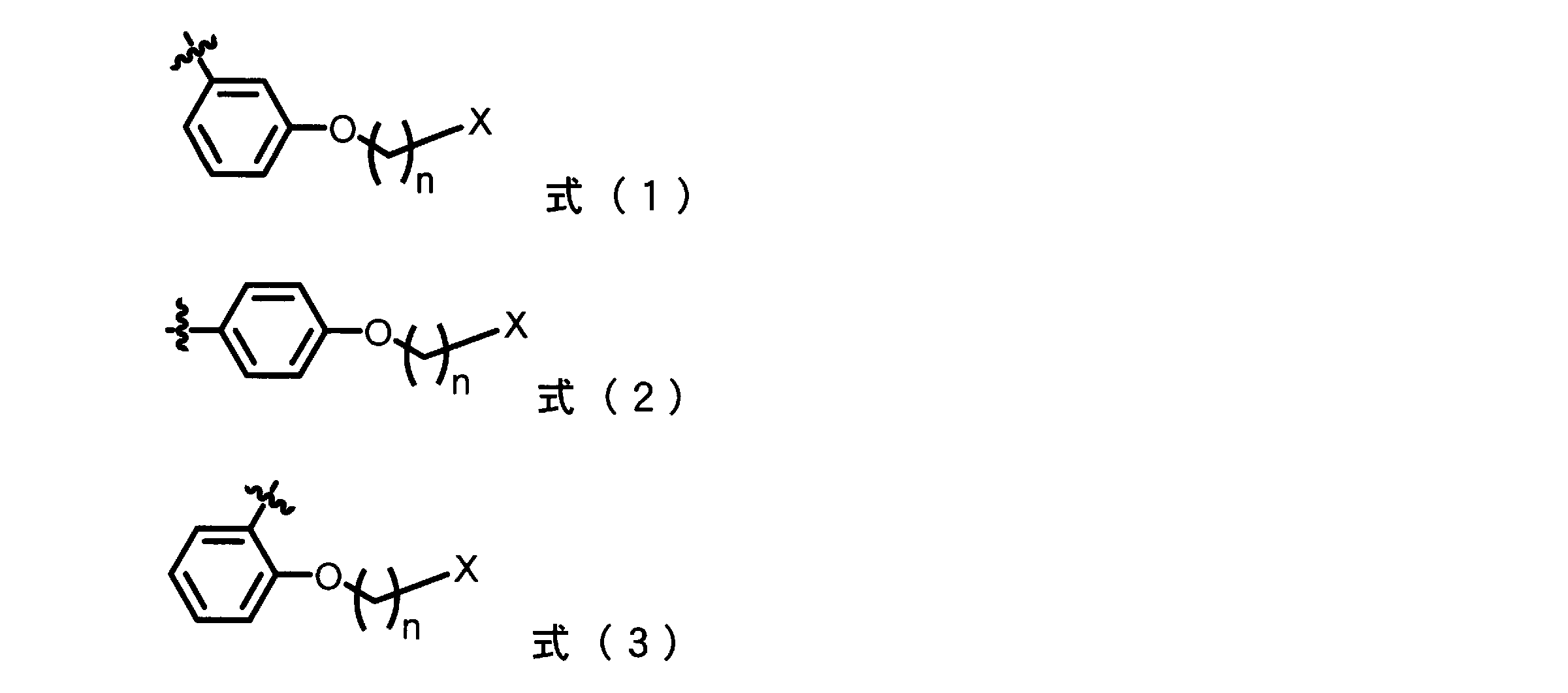

(電荷輸送性ポリマーI)
電荷輸送性ポリマーIは、電荷を輸送する能力を有する。実施形態の有機エレクトロニクス材料Iにおいて、電荷輸送性ポリマーIは、重合性官能基Xを有する、上記式(1)、式(2)、及び式(3)からなる群から選択される少なくとも1つの構造を含む(以下、式(1)の構造、式(2)の構造及び式(3)の構造をそれぞれ式(1)で表される構造、式(2)で表される構造及びは式(3)で表される構造ともいう。)。電荷輸送性ポリマーIは、式(1)、(2)、又は(3)で表される構造を複数含んでいてもよい。式(1)、(2)、又は(3)で表される構造を複数含む場合は、それらの構造は同一であっても異なってもよい。
ポリマー分子同士の結合距離を短縮し、ホッピングによるキャリア輸送性を高める観点からはnは、あまり大きくないほうが好ましい。nは、12以下が好ましいが、例えば、8以下であってもよく、4以下であってもよい。
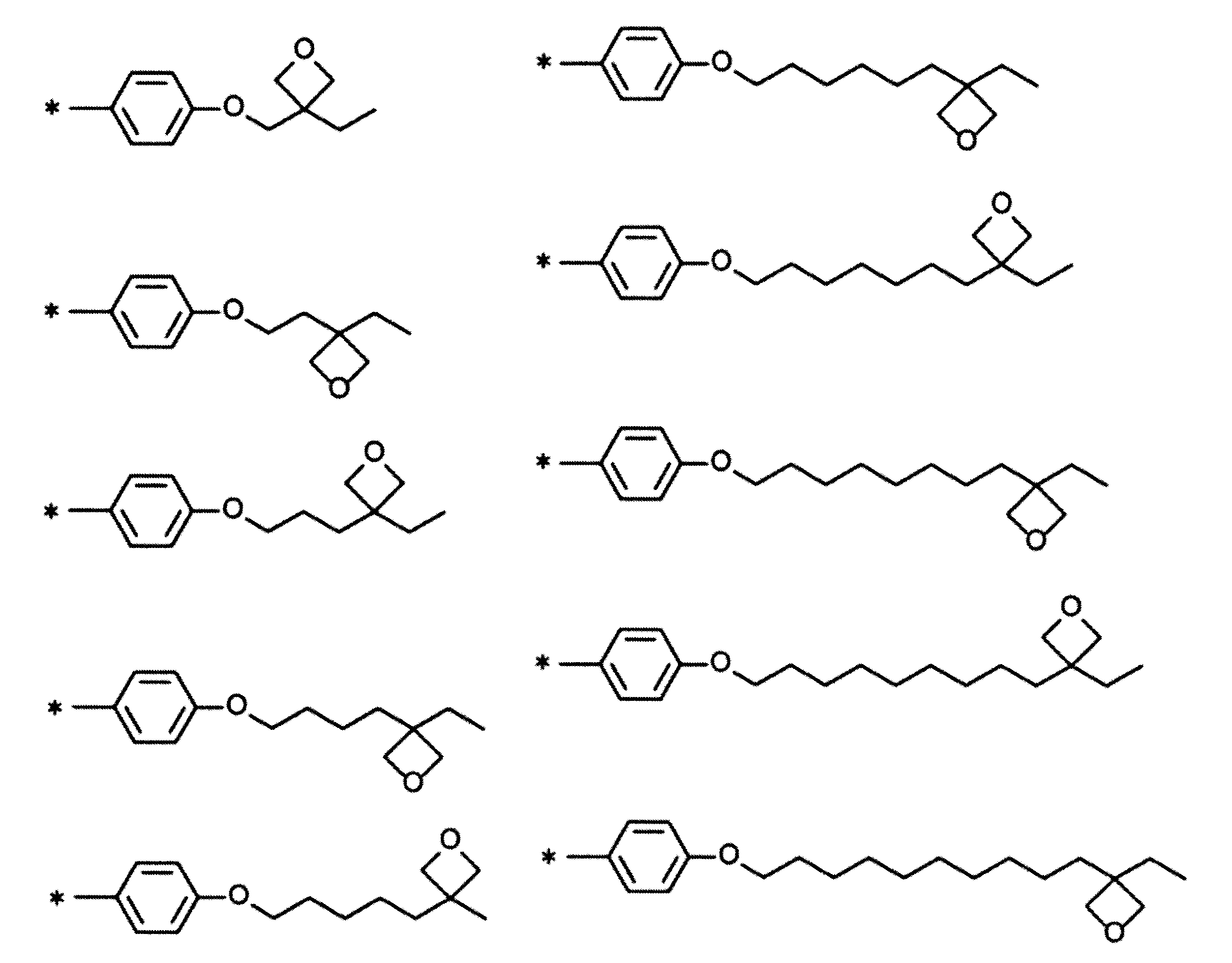


電荷輸送性ポリマーIIは、電荷を輸送する能力を有する。実施形態の有機エレクトロニクス材料IIにおいて、電荷輸送性ポリマーIIは、重合性官能基Xaを有する、上記式(1a)、式(2a)、及び式(3a)からなる群から選択される少なくとも1つの構造を含む(以下、式(1a)の構造、式(2a)の構造及び式(3a)の構造をそれぞれ式(1a)で表される構造、式(2a)で表される構造及びは式(3a)で表される構造ともいう。)。電荷輸送性ポリマーIIは、式(1a)、(2a)、又は(3a)で表される構造を複数含んでいてもよい。式(1a)、(2a)、又は(3a)で表される構造を複数含む場合は、それらの構造は同一であっても異なってもよい。
重合性官能基Xaとしては、特に、置換又は非置換の、ビニル基、アクリロイル基、メタクリロイル基、エポキシ基、及びオキセタン基が好ましく、反応性及び有機エレクトロニクス素子の特性の観点から、置換又は非置換の、ビニル基、オキセタン基、又はエポキシ基がより好ましく、置換又は非置換のオキセタン基が最も好ましい。置換又は非置換のオキセタン基の例としては、下記の重合性官能基Xaの具体例に示されるものが挙げられる。


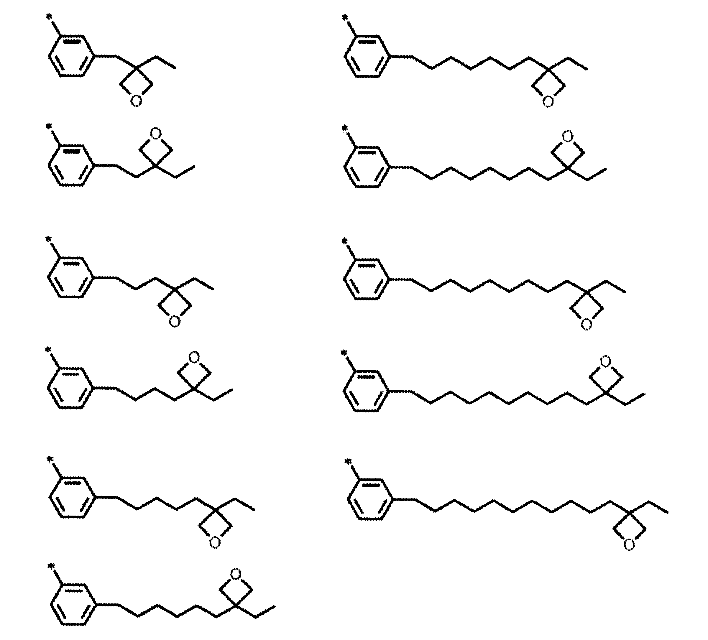
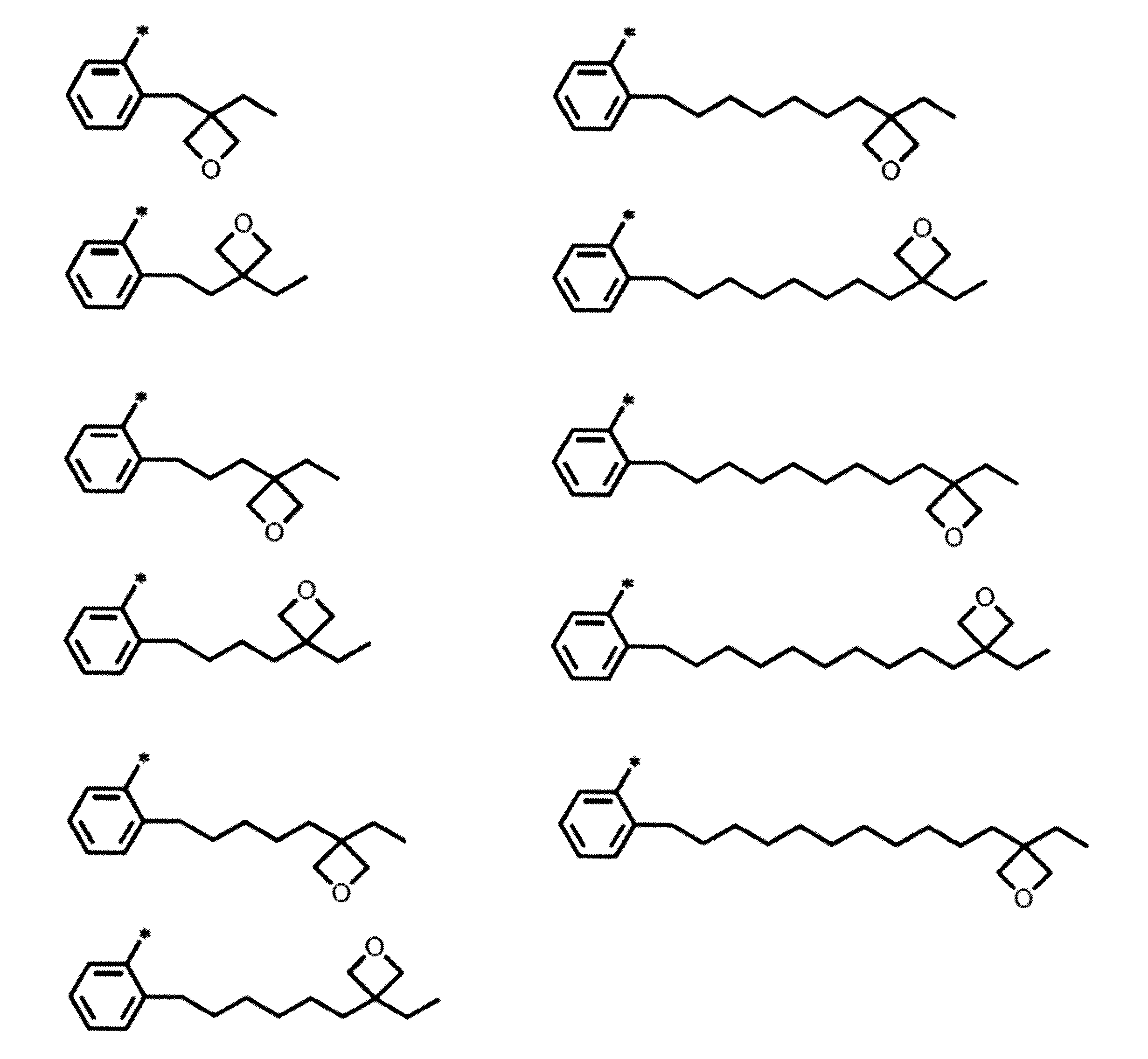

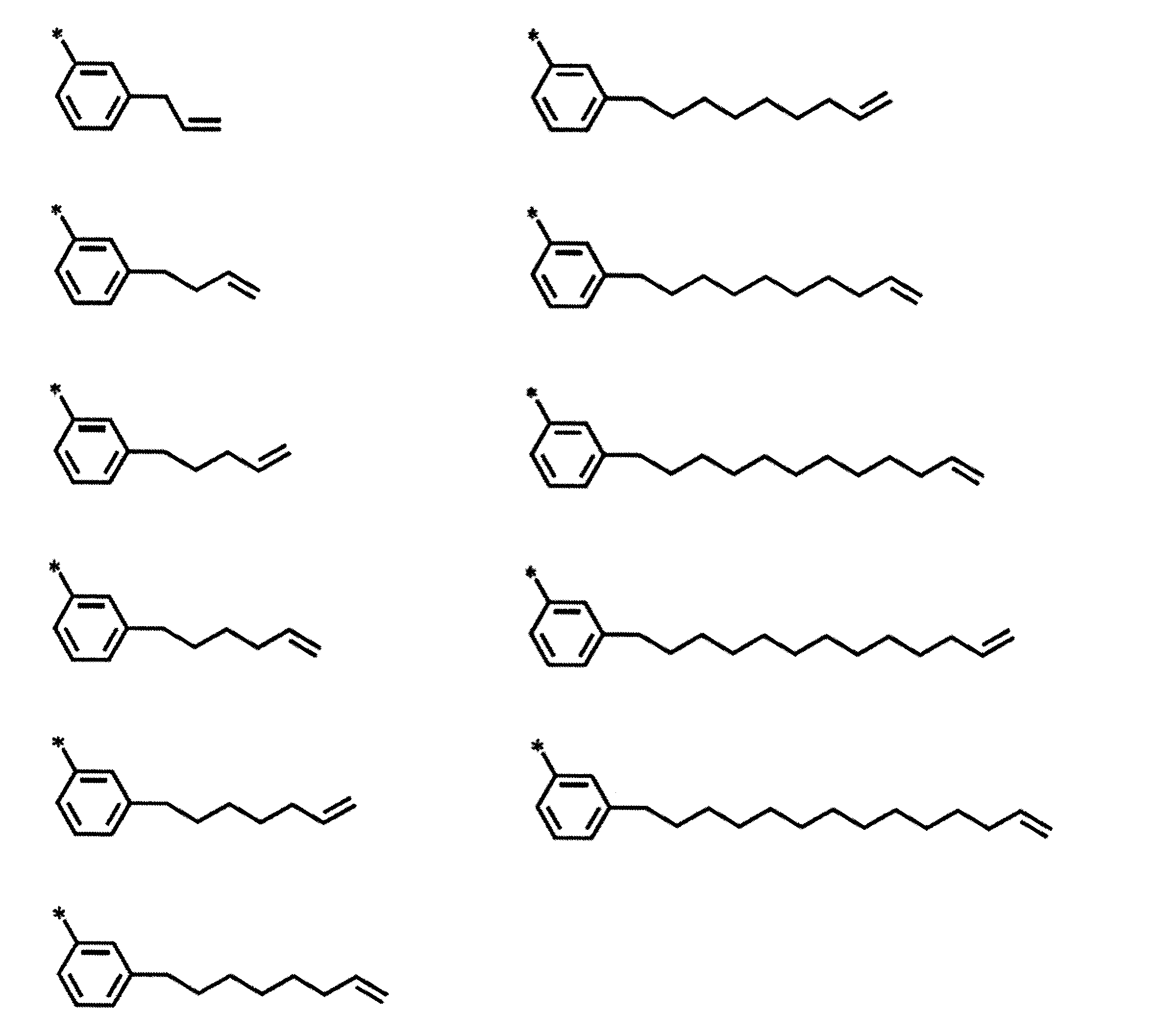

以下に、実施形態における電荷輸送性ポリマーI及びIIの構造を具体的に説明する。


構造単位Lは、電荷輸送性を有する2価の構造単位である。構造単位Lは、電荷を輸送する能力を有する原子団を含んでいればよく、特に限定されない。例えば、構造単位Lは、置換又は非置換の、芳香族アミン構造、カルバゾール構造、チオフェン構造、フルオレン構造、ベンゼン構造、ビフェニル構造、ターフェニル構造、ナフタレン構造、アントラセン構造、テトラセン構造、フェナントレン構造、ジヒドロフェナントレン構造、ピリジン構造、ピラジン構造、キノリン構造、イソキノリン構造、キノキサリン構造、アクリジン構造、ジアザフェナントレン構造、フラン構造、ピロール構造、オキサゾール構造、オキサジアゾール構造、チアゾール構造、チアジアゾール構造、トリアゾール構造、ベンゾチオフェン構造、ベンゾオキサゾール構造、ベンゾオキサジアゾール構造、ベンゾチアゾール構造、ベンゾチアジアゾール構造、ベンゾトリアゾール構造、及び、これらの1種又は2種以上を含む構造から選択される。芳香族アミン構造は、好ましくはトリアリールアミン構造であり、より好ましくはトリフェニルアミン構造である。
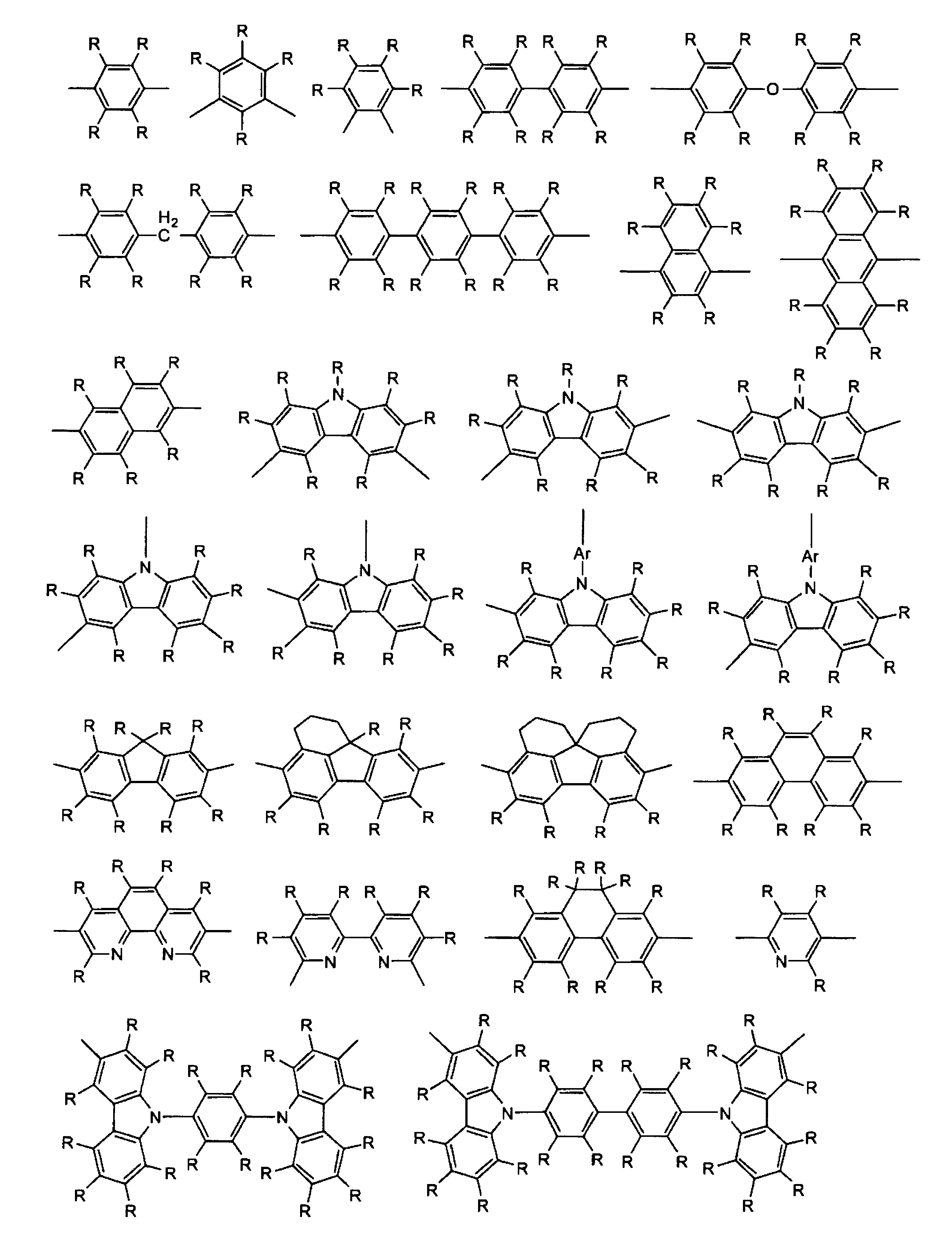

R1~R8は、それぞれ独立に、水素原子;炭素数1~22個の直鎖、環状又は分岐アルキル基;又は、炭素数2~30個のアリール基又はヘテロアリール基を表す。アルキル基は、更に、炭素数2~20個のアリール基又はヘテロアリール基により置換されていてもよく、アリール基又はヘテロアリール基は、更に、炭素数1~22個の直鎖、環状又は分岐アルキル基により置換されていてもよい。
Rは、好ましくは水素原子、アルキル基、アリール基、アルキル置換アリール基である。
構造単位Tは、電荷輸送性ポリマーの末端部を構成する1価の構造単位である。構造単位Tは、特に限定されず、例えば、置換又は非置換の、芳香族炭化水素構造、芳香族複素環構造、及び、これらの1種又は2種以上を含む構造から選択される。一実施形態において、構造単位Tは、電荷の輸送性を低下させずに耐久性を付与するという観点から、置換又は非置換の芳香族炭化水素構造であることが好ましく、置換又は非置換のベンゼン構造であることがより好ましい。また、他の実施形態において、電荷輸送性ポリマーが末端部に重合性官能基を有する場合、構造単位Tは重合可能な構造(例えば、ピロール-イル基等の重合性官能基)であってもよい。構造単位Tは、構造単位Lと同じ構造を有していても、又は、異なる構造を有していてもよい。


構造単位Bは、電荷輸送性ポリマーが分岐構造を有する場合に、分岐部を構成する3価以上の構造単位である。構造単位Bは、有機エレクトロニクス素子の耐久性向上の観点から、好ましくは6価以下であり、より好ましくは3価又は4価である。構造単位Bは、電荷輸送性を有する単位であることが好ましい。例えば、構造単位Bは、有機エレクトロニクス素子の耐久性向上の観点から、置換又は非置換の、芳香族アミン構造、カルバゾール構造、縮合多環式芳香族炭化水素構造、及び、これらの1種又は2種以上を含有する構造から選択される。構造単位Bは、構造単位Lと同じ構造を有していても、又は、異なる構造を有していてもよく、また、構造単位Tと同じ構造を有していても、又は、異なる構造を有していてもよい。
複数のベンゼン環が縮合した多環芳香族の例として、ナフタレン、アントラセン、フェナントレン、ピレン、ベンゾピレン等が挙げられる。
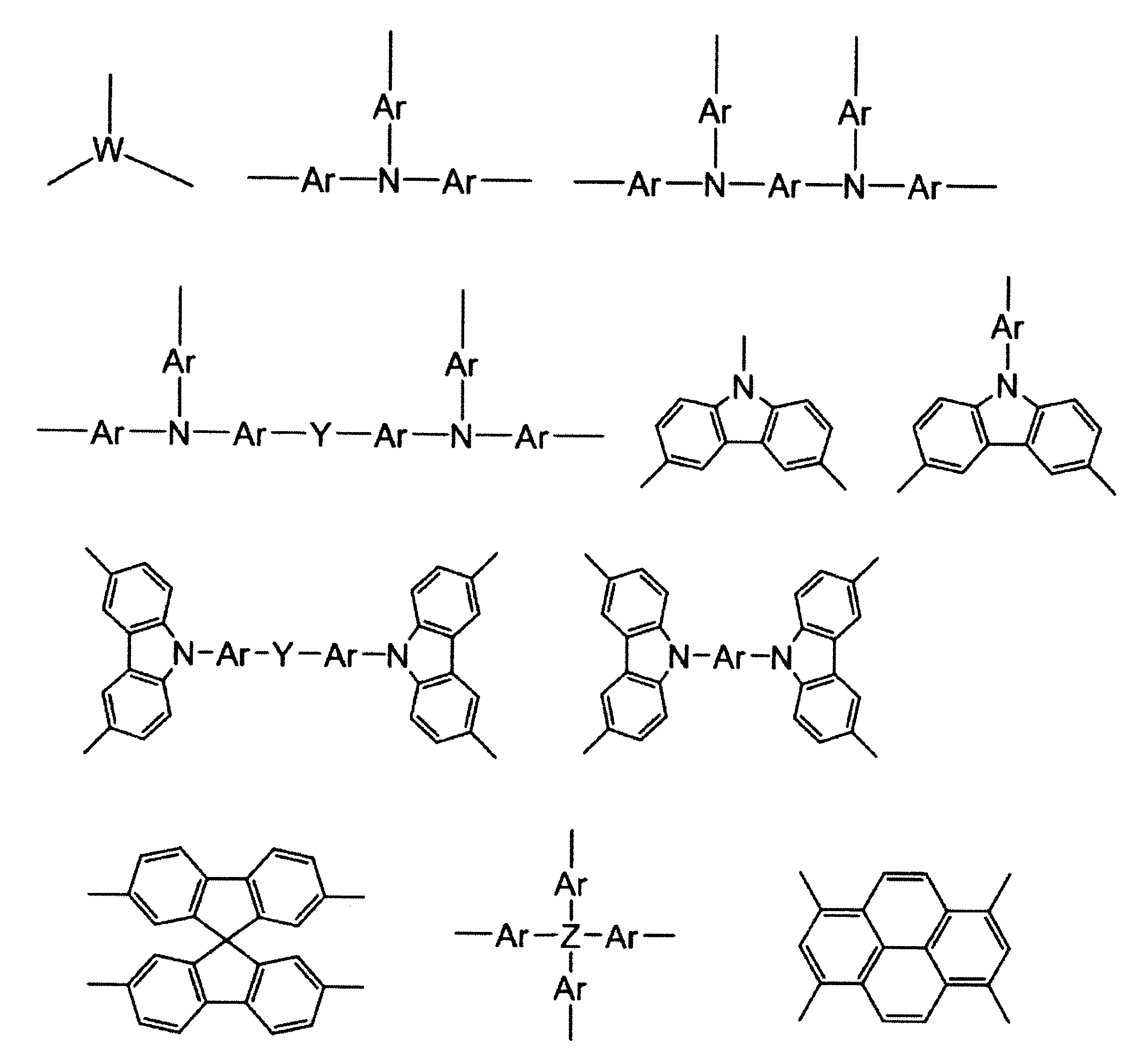
電荷輸送性ポリマーIに含まれる構造単位Lの割合は、十分な電荷輸送性を得る観点から、全構造単位を基準として、10モル%以上が好ましく、20モル%以上がより好ましく、30モル%以上が更に好ましい。また、電荷輸送性ポリマーIに含まれる構造単位Lの割合は、構造単位T及び必要に応じて導入される構造単位Bを考慮すると、95モル%以下が好ましく、90モル%以下がより好ましく、85モル%以下が更に好ましい。
電荷輸送性ポリマーIIに含まれる構造単位Lの割合の好ましい範囲は、上述の電荷輸送ポリマーIに含まれる構造単位Lの割合の好ましい範囲と同様である。
電荷輸送性ポリマーIIに含まれる構造単位Tの割合の好ましい範囲は、上述の電荷輸送ポリマーIに含まれる構造単位Lの割合の好ましい範囲と同様である。
電荷輸送性ポリマーIIが構造単位Bを含む場合、電荷輸送性ポリマーIIに含まれる構造単位Bの割合の好ましい範囲は、上述の、電荷輸送性ポリマーIが構造単位Bを含む場合の電荷輸送性ポリマーIに含まれる構造単位Lの割合の好ましい範囲と同様である。
電荷輸送性ポリマーIIにおける構造単位L及び構造単位Tの割合(モル比)の好ましい割合、及び、電荷輸送性ポリマーIIが構造単位Bを含む場合の、構造単位L、構造単位T、及び構造単位Bの割合(モル比)の好ましい範囲は、上述の、電荷輸送性ポリマーIおける構造単位L及び構造単位Tの割合(モル比)の好ましい割合、及び、電荷輸送性ポリマーIが構造単位Bを含む場合の、構造単位L、構造単位T、及び構造単位Bの割合(モル比)の好ましい範囲と同様である。
電荷輸送性ポリマーI及び電荷輸送性ポリマーIIの数平均分子量は、それぞれ、溶剤への溶解性、成膜性等を考慮して適宜、調整できる。
電荷輸送性ポリマーIの数平均分子量は、電荷輸送性に優れるという観点から、500以上が好ましく、1,000以上がより好ましく、2,000以上が更に好ましい。また、電荷輸送性ポリマーIの数平均分子量は、溶媒への良好な溶解性を保ち、インク組成物の調製を容易にするという観点から、1,000,000以下が好ましく、100,000以下がより好ましく、50,000以下が更に好ましい。
電荷輸送性ポリマーIIの数平均分子量の好ましい範囲は、上述の、電荷輸送性ポリマーIの数平均分子量の好ましい範囲と同様である。
電荷輸送性ポリマーI及びIIのそれぞれにおいて、電荷輸送性ポリマーの重量平均分子量は、溶剤への溶解性、成膜性等を考慮して適宜、調整できる。
電荷輸送性ポリマーIの重量平均分子量は、電荷輸送性に優れるという観点から、1,000以上が好ましく、5,000以上がより好ましく、10,000以上が更に好ましい。また、電荷輸送性ポリマーIの重量平均分子量は、溶媒への良好な溶解性を保ち、インク組成物の調製を容易にするという観点から、1,000,000以下が好ましく、700,000以下がより好ましく、400,000以下が更に好ましい。
電荷輸送性ポリマーIIの重量平均分子量の好ましい範囲は、上述の、電荷輸送性ポリマーIの重量平均分子量の好ましい範囲と同様である。
装置:高速液体クロマトグラフ Prominence(株)島津製作所
送液ポンプ(LC-20AD)
脱気ユニット(DGU-20A)
オートサンプラ(SIL-20AHT)
カラムオーブン(CTO-20A)
PDA検出器(SPD-M20A)
示差屈折率検出器(RID-20A)
カラム:Gelpack(登録商標)
GL-A160S/GL-A150S 日立化成(株)
溶離液:テトラヒドロフラン(THF)(HPLC用、安定剤含有)和光純薬工業(株)
流速:1mL/min
カラム温度:40℃
検出波長:254nm
分子量標準物質:標準ポリスチレンキットPStQuick A/B/C 東ソー(株)
本実施形態の電荷輸送性ポリマーI及びIIは、それぞれ、正孔輸送性を有する構造単位を含むモノマーの重合体又は共重合体であることが好ましい。電荷輸送性ポリマーI及びIIは、それぞれ、好ましくは、上記構造単位Lを含む一種以上のモノマーと、上記構造単位Tを含む一種以上のモノマーとを含み、任意に上記構造単位Bを含むモノマーを含むモノマー混合物を用いて、これらのモノマーを共重合させることにより、好ましく製造することができる。共重合の形式は、交互、ランダム、ブロック又はグラフト共重合体であってもよいし、それらの中間的な構造を有する共重合体、例えばブロック性を帯びたランダム共重合体であってもよい。
有機エレクトロニクス材料I及びIIは、それぞれ、任意の添加剤を含むことができ、例えばドーパントを更に含有してよい、ドーパントは、有機エレクトロニクス材料に添加することでドーピング効果を発現させ、電荷の輸送性を向上させ得るものであればよく、特に制限はない。ドーピングには、p型ドーピングとn型ドーピングがあり、p型ドーピングではドーパントとして電子受容体として働く物質が用いられ、n型ドーピングではドーパントとして電子供与体として働く物質が用いられる。正孔輸送性の向上にはp型ドーピング、電子輸送性の向上にはn型ドーピングを行うことが好ましい。有機エレクトロニクス材料に用いられるドーパントは、p型ドーピング又はn型ドーピングのいずれの効果を発現させるドーパントであってもよい。また、1種のドーパントを単独で添加しても、複数種のドーパントを混合して添加してもよい。
また、上記イオン化合物として、例えば、オニウム塩が挙げられる。オニウム塩とは、ヨードニウム、アンモニウム等のカチオンと対アニオンからなる化合物を言う。
有機エレクトロニクス材料I及びIIは、それぞれ、電荷輸送性低分子化合物、他のポリマー等を更に含有してもよい。
有機エレクトロニクス材料I中の電荷輸送性ポリマーIの含有量は、良好な電荷輸送性を得る観点から、有機エレクトロニクス材料Iの全質量に対して50質量%以上であることが好ましく、70質量%以上がより好ましく、80質量%以上が更に好ましい。有機エレクトロニクス材料I中の電荷輸送性ポリマーIの含有量の上限は特に限定されず、100質量%とすることも可能である。ドーパント等の添加剤を含むことを考慮し、有機エレクトロニクス材料I中の電荷輸送性ポリマーIの含有量を、例えば99質量%以下、98質量%以下、95質量%以下、90質量%以下、等としてもよい。
有機エレクトロニクス材料II中の電荷輸送性ポリマーのII含有量は、良好な電荷輸送性を得る観点から、有機エレクトロニクス材料IIの全質量に対して50質量%以上であることが好ましく、70質量%以上がより好ましく、80質量%以上が更に好ましい。有機エレクトロニクス材料II中の電荷輸送性ポリマーIIの含有量の上限は特に限定されず、100質量%とすることも可能である。ドーパント等の添加剤を含むことを考慮し、有機エレクトロニクス材料II中の電荷輸送性ポリマーIIの含有量を、例えば99質量%以下、98質量%以下、95質量%以下、90質量%以下、等としてもよい。
有機エレクトロニクス材料IIがドーパントを含有する場合、その含有量は、有機エレクトロニクス材料IIの電荷輸送性を向上させる観点から、有機エレクトロニクス材料IIの全質量に対して、0.01質量%以上が好ましく、0.1質量%以上がより好ましく、0.5質量%以上が更に好ましい。また、成膜性を良好に保つ観点から、有機エレクトロニクス材料IIの全質量に対して、50質量%以下が好ましく、30質量%以下がより好ましく、20質量%以下が更に好ましい。
前記実施形態の有機エレクトロニクス材料I及びIIは、それぞれ、さらに該材料を溶解又は分散し得る溶媒を含有するインク組成物であってよい。このようなインク組成物を用いることによって、塗布法といった簡便な方法によって有機層を容易に形成できる。
溶媒としては、水、有機溶媒、又はこれらの混合溶媒を使用できる。有機溶媒としては、メタノール、エタノール、イソプロピルアルコール等のアルコール;ペンタン、ヘキサン、オクタン等のアルカン;シクロヘキサン等の環状アルカン;ベンゼン、トルエン、キシレン、メシチレン、テトラリン、ジフェニルメタン等の芳香族炭化水素;エチレングリコールジメチルエーテル、エチレングリコールジエチルエーテル、プロピレングリコール-1-モノメチルエーテルアセタート等の脂肪族エーテル;1,2-ジメトキシベンゼン、1,3-ジメトキシベンゼン、アニソール、フェネトール、2-メトキシトルエン、3-メトキシトルエン、4-メトキシトルエン、2,3-ジメチルアニソール、2,4-ジメチルアニソール等の芳香族エーテル;酢酸エチル、酢酸n-ブチル、乳酸エチル、乳酸n-ブチル等の脂肪族エステル;酢酸フェニル、プロピオン酸フェニル、安息香酸メチル、安息香酸エチル、安息香酸プロピル、安息香酸n-ブチル等の芳香族エステル;N,N-ジメチルホルムアミド、N,N-ジメチルアセトアミド等のアミド系溶媒;ジメチルスルホキシド、テトラヒドロフラン、アセトン、クロロホルム、塩化メチレンなどが挙げられる。好ましくは、芳香族炭化水素、脂肪族エステル、芳香族エステル、脂肪族エーテル、芳香族エーテル等である。
インク組成物は、好ましくは、重合開始剤を含有する。重合開始剤として、公知のラジカル重合開始剤、カチオン重合開始剤、アニオン重合開始剤等を使用できる。インク組成物を簡便に調製できる観点から、ドーパントとしての機能と重合開始剤としての機能とを兼ねる物質を用いることが好ましい。そのような物質として、例えば、前記イオン化合物が挙げられる。また、カチオン重合開始剤として、前記オニウム塩を好ましく用いることができる。
インク組成物は、更に、任意成分として添加剤を含有してもよい。添加剤としては、例えば、重合禁止剤、安定剤、増粘剤、ゲル化剤、難燃剤、酸化防止剤、還元防止剤、酸化剤、還元剤、表面改質剤、乳化剤、消泡剤、分散剤、界面活性剤等が挙げられる。
インク組成物における溶媒の含有量は、種々の塗布方法へ適用することを考慮して定めることができる。例えば、溶媒の含有量は、溶媒に対し電荷輸送性ポリマーの割合が、0.1質量%以上となる量が好ましく、0.2質量%以上となる量がより好ましく、0.5質量%以上となる量が更に好ましい。また、溶媒の含有量は、溶媒に対し電荷輸送性ポリマーの割合が、20質量%以下となる量が好ましく、15質量%以下となる量がより好ましく、10質量%以下となる量が更に好ましい。
本発明の実施形態である有機層は、前記実施形態の有機エレクトロニクス材料又はインク組成物を用いて形成された層である。インク組成物を用いることによって、塗布法により有機層を良好かつ簡便に形成できる。塗布方法としては、例えば、スピンコーティング法;キャスト法;浸漬法;凸版印刷、凹版印刷、オフセット印刷、平版印刷、凸版反転オフセット印刷、スクリーン印刷、グラビア印刷等の有版印刷法;インクジェット法等の無版印刷法などの公知の方法が挙げられる。塗布法によって有機層を形成する場合、塗布後に得られた有機層(塗布層)を、ホットプレート又はオーブンを用いて乾燥させ、溶媒を除去してもよい。
本発明の実施形態である有機エレクトロニクス素子は、少なくとも一つ以上の前記実施形態の有機層を有する。有機エレクトロニクス素子として、例えば、有機EL素子、有機光電変換素子、有機トランジスタ等が挙げられる。有機エレクトロニクス素子は、好ましくは、少なくとも一対の電極の間に有機層が配置された構造を有する。
本発明の実施形態である有機EL素子は、少なくとも一つ以上の前記実施形態の有機層を有する。有機EL素子は、通常、発光層、陽極、陰極、及び基板を備えており、必要に応じて、正孔注入層、電子注入層、正孔輸送層、電子輸送層等の他の機能層を備えている。各層は、蒸着法により形成してもよく、塗布法により形成してもよい。有機EL素子は、好ましくは、前記有機層を発光層又は他の機能層として有し、より好ましくは機能層として有し、更に好ましくは正孔注入層及び正孔輸送層の少なくとも一方として有する。
発光層に用いる材料として、低分子化合物、ポリマー、デンドリマー等の発光材料を使用できる。ポリマーは、溶媒への溶解性が高く、塗布法に適しているため好ましい。発光材料としては、蛍光材料、燐光材料、熱活性化遅延蛍光材料(TADF)等が挙げられる。
上記の有機エレクトロニクス材料を用いて形成された有機層を、正孔注入層及び正孔輸送層の少なくとも一方として使用することが好ましく、少なくとも正孔輸送層として使用することが一層好ましい。上述のとおり、有機エレクトロニクス材料を含むインク組成物を用いることにより、これらの層を容易に形成することができる。
電子輸送層及び電子注入層に用いる材料としては、例えば、フェナントロリン誘導体、ビピリジン誘導体、ニトロ置換フルオレン誘導体、ジフェニルキノン誘導体、チオピランジオキシド誘導体、ナフタレン、ペリレンなどの縮合環テトラカルボン酸無水物、カルボジイミド、フルオレニリデンメタン誘導体、アントラキノジメタン及びアントロン誘導体、オキサジアゾール誘導体、チアジアゾール誘導体、ベンゾイミダゾール誘導体、キノキサリン誘導体、アルミニウム錯体等が挙げられる。また、前記実施形態の有機エレクトロニクス材料も使用できる。
陰極材料としては、例えば、Li、Ca、Mg、Al、In、Cs、Ba、Mg/Ag、LiF、CsF等の金属又は金属合金が用いられる。
陽極材料としては、例えば、金属(例えば、Au)又は導電性を有する他の材料が用いられる。他の材料として、例えば、酸化物(例えば、ITO:酸化インジウム/酸化錫)、導電性高分子(例えば、ポリチオフェン-ポリスチレンスルホン酸混合物(PEDOT:PSS))が挙げられる。
基板として、ガラス、プラスチック等を使用できる。基板は、透明であることが好ましく、また、フレキシブル性を有するフレキシブル基板であることが好ましい。石英ガラス、光透過性樹脂フィルム等が好ましく用いられる。
有機EL素子は、外気の影響を低減させて長寿命化させるため、封止されていてもよい。封止に用いる材料としては、ガラス、エポキシ樹脂、アクリル樹脂、ポリエチレンテレフタレート、ポリエチレンナフタレート等のプラスチックフィルム、又は酸化珪素、窒化ケイ素等の無機物を用いることができるが、これらに限定されることはない。
封止の方法も、特に限定されず、公知の方法で行うことができる。
有機EL素子の発光色は特に限定されるものではない。白色の有機EL素子は、家庭用照明、車内照明、時計又は液晶のバックライト等の各種照明器具に用いることができるため好ましい。
本発明の実施形態である表示素子は、前記実施形態の有機EL素子を備えている。例えば、赤、緑及び青(RGB)の各画素に対応する素子として、有機EL素子を用いることで、カラーの表示素子が得られる。画像の形成方法には、マトリックス状に配置した電極でパネルに配列された個々の有機EL素子を直接駆動する単純マトリックス型と、各素子に薄膜トランジスタを配置して駆動するアクティブマトリックス型とがある。

<2> 前記電荷輸送性ポリマーが、前記(1)、式(2)、及び式(3)からなる群から選択される少なくとも1つの構造を末端に有する、<1>に記載の有機エレクトロニクス材料。

<4> 前記電荷輸送性ポリマーが、前記(1a)、式(2a)、及び式(3a)からなる群から選択される少なくとも1つの構造を末端に有する、<3>に記載の有機エレクトロニクス材料。
<6> 前記電荷輸送性ポリマーが、置換又は非置換の、芳香族アミン構造、カルバゾール構造、チオフェン構造、ビチオフェン構造、ベンゼン構造、複数のベンゼン環が縮合した多環芳香族構造、及びフルオレン構造からなる群から選択される構造を含む2価の構造単位を含む、<1>~<5>のいずれか一項に記載の有機エレクトロニクス材料。
<7> 前記電荷輸送性ポリマーが正孔輸送材料である、<1>~<6>のいずれか一項に記載の有機エレクトロニクス材料。
<8> さらに重合開始剤を含む、<1>~<7>のいずれか一項に記載の有機エレクトロニクス材料。
<9> 前記重合開始剤がカチオン重合開始剤を含む、<8>に記載の有機エレクトロニクス材料。
<10> 前記カチオン重合開始剤がオニウム塩を含む、<9>に記載の有機エレクトロニクス材料。
<12> <11>に記載の有機層を含む、有機エレクトロニクス素子。
<13> <11>に記載の有機層を含む、有機エレクトロルミネセンス素子。
<14> 燐光材料を含む発光層を有する、<13>に記載の有機エレクトロルミネセンス素子。
<15> 遅延蛍光材料を含む発光層を有する、<13>に記載の有機エレクトロルミネセンス素子。
<16> フレキシブル基板をさらに有する、<13>~<15>のいずれか一項に記載の有機エレクトロルミネセンス素子。
<17> 樹脂フィルム基板をさらに有する、<13>~<15>のいずれか一項に記載の有機エレクトロルミネセンス素子。
<18> <13>~<17>のいずれか一項に記載の有機エレクトロルミネセンス素子を備えた、表示素子。
<19> <13>~<17>のいずれか一項に記載の有機エレクトロルミネセンス素子を備えた、照明装置。
<20> 19に記載の照明装置と、表示手段として液晶素子とを備えた、表示装置。
窒素雰囲気下のグローブボックス中で、室温下、サンプル管にトリス(ジベンジリデンアセトン)ジパラジウム(73.2mg、80μmol)を秤取り、アニソール(15ml)を加え、30分間攪拌した。同様に、サンプル管にトリス(t-ブチル)ホスフィン(129.6mg、640μmol)を秤取り、アニソール(5mL)を加え、5分間攪拌した。これらの溶液を混合し、室温で30分間攪拌して、触媒の溶液を得た。なお、触媒の調製において、すべての溶媒は、30分以上窒素バブルにより脱気した後に使用した。
<電荷輸送性ポリマーの合成>
表1に示す電荷輸送性ポリマーは次の手順で合成した。表1に示すように、下記ブロモモノマー、下記ボロン酸モノマー、下記重合性モノマー、下記末端モノマーを組み合わせて各種ポリマーを合成した。三口丸底フラスコに、ボロン酸モノマー(4.0mmol)、ブロモモノマー(5.0mmol)、重合性モノマー(重合性モノマー100%の場合:2.0mmol、重合性モノマー50%の場合:1.0mmol)、末端モノマー(重合性モノマー100%の場合:0mmol、重合性モノマー50%の場合:1.0mmol)、及びアニソール(20mL)を加え、さらに、上記調製したPd触媒溶液(7.5mL)を加えた。30分撹拌した後、10%テトラエチルアンモニウム水酸化物水溶液(20mL)を追加した。この混合物を2時間、加熱・還流した。なお、ここまでの全ての操作は、窒素気流下で行った。また、すべての溶媒は、30分以上窒素バブルにより脱気した後に使用した。


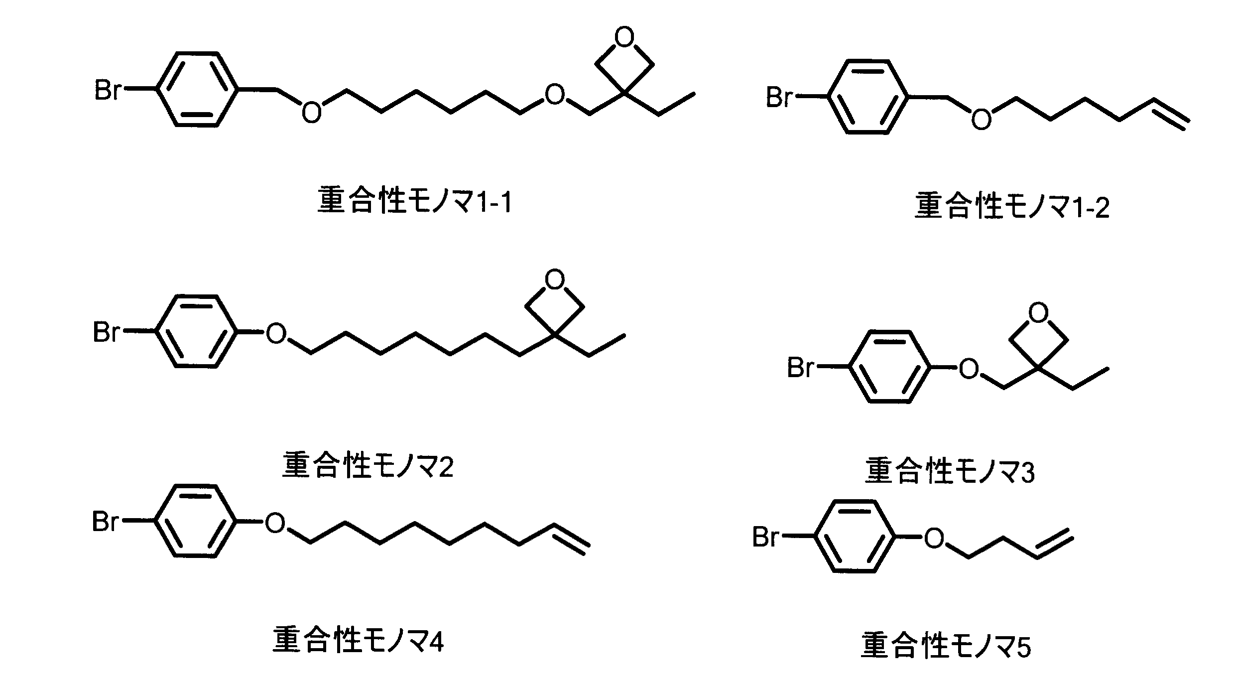
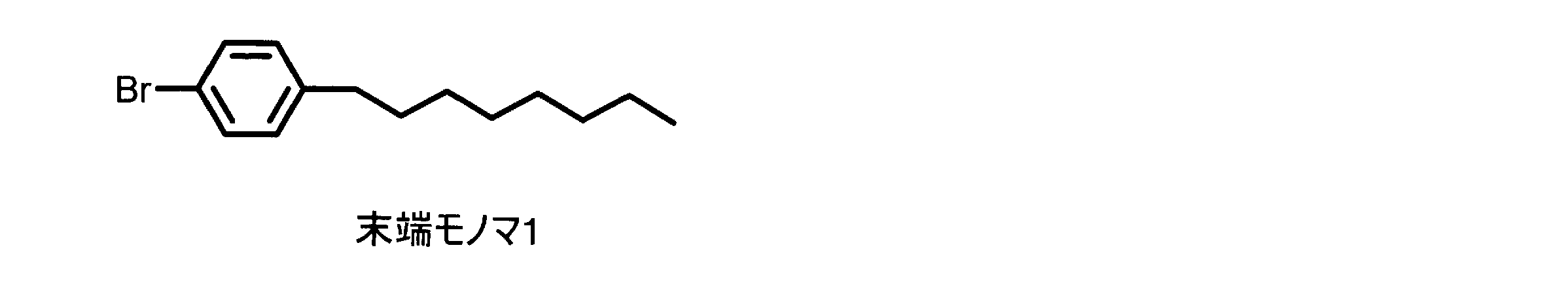
装置:高速液体クロマトグラフ Prominence(株)島津製作所
送液ポンプ(LC-20AD)
脱気ユニット(DGU-20A)
オートサンプラ(SIL-20AHT)
カラムオーブン(CTO-20A)
PDA検出器(SPD-M20A)
示差屈折率検出器(RID-20A)
カラム:Gelpack(登録商標)
GL-A160S(製造番号:686-1J27)
GL-A150S(製造番号:685-1J27)日立化成(株)
溶離液:テトラヒドロフラン(THF)(HPLC用、安定剤含有)和光純薬工業(株)
流速:1mL/min
カラム温度:40℃
検出波長:254nm
分子量標準物質:標準ポリスチレンキットPStQuick A/B/C 東ソー(株)


表3の比較例1~14、及び実施例1~32に示す有機EL素子を次の手順で作製した。ITOを1.6mm幅にパターンニングしたガラス基板上に、PEDOT:PSS分散液(シュタルク・ヴィテック社製、AI4083 LVW142)を、回転速度1500min-1でスピン塗布し、ホットプレート上で空気中、200℃/10分加熱乾燥して、正孔注入層(40nm)を形成した。以後の実験は乾燥窒素環境下で行った。


<電荷輸送性ポリマーの合成>
表4に示す電荷輸送性ポリマーは次の手順で合成した。表4に示すように、下記ブロモモノマー、下記ボロン酸モノマー、下記重合性モノマー、下記末端モノマーを組み合わせて各種ポリマーを合成した。三口丸底フラスコに、ボロン酸モノマー(4.0mmol)、ブロモモノマー(5.0mmol)、重合性モノマー(重合性モノマー100%の場合:2.0mmol、重合性モノマー50%の場合:1.0mmol)、末端モノマー(重合性モノマー100%の場合:0mmol、重合性モノマー50%の場合:1.0mmol、重合性モノマー25%の場合:1.5mmol)、及びアニソール(20mL)を加え、さらに、上記調製したPd触媒溶液(7.5mL)を加えた。30分撹拌した後、10%テトラエチルアンモニウム水酸化物水溶液(20mL)を追加した。この混合物を2時間、加熱・還流した。なお、ここまでの全ての操作は、窒素気流下で行った。また、すべての溶媒は、30分以上窒素バブルにより脱気した後に使用した。

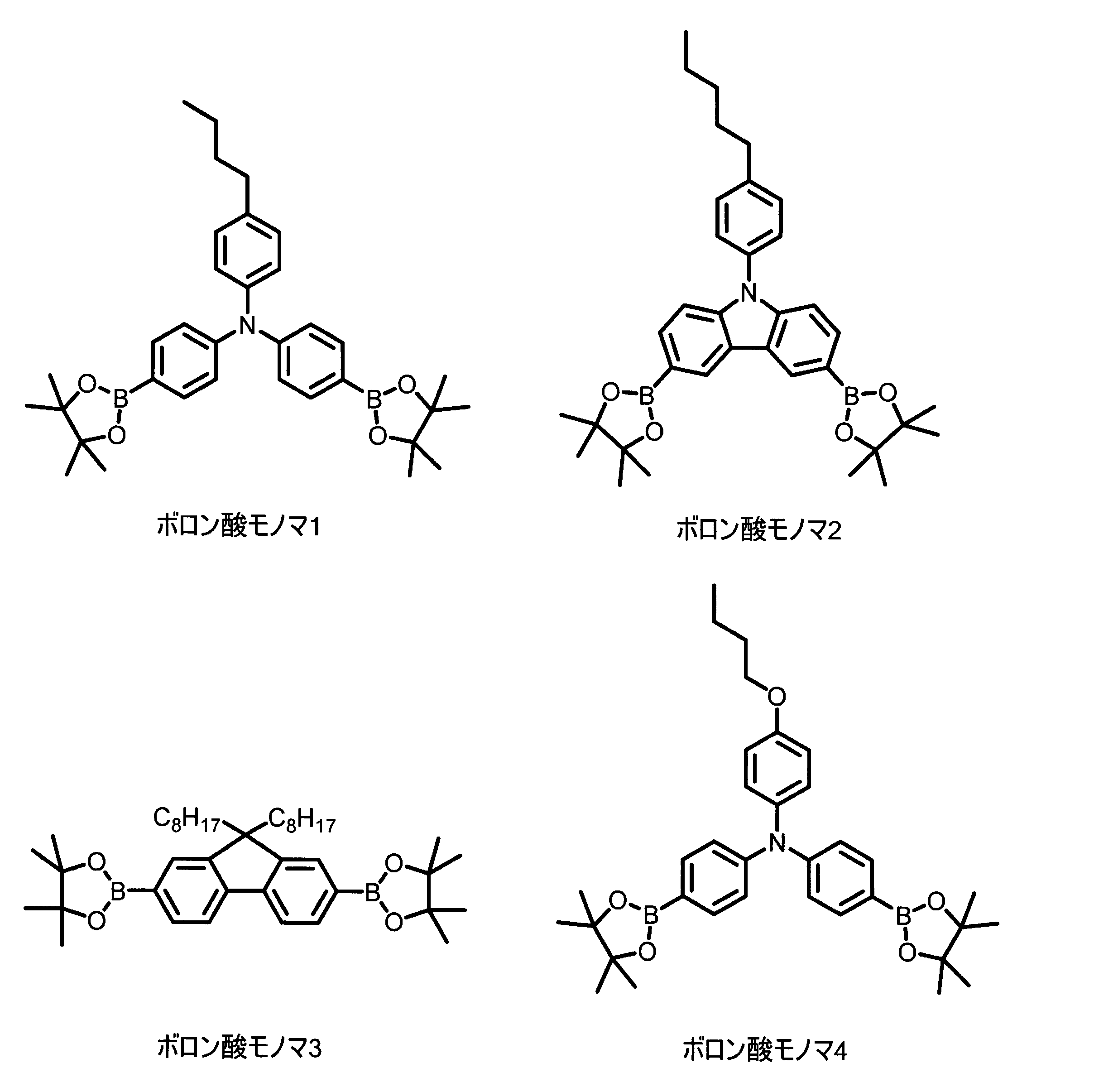
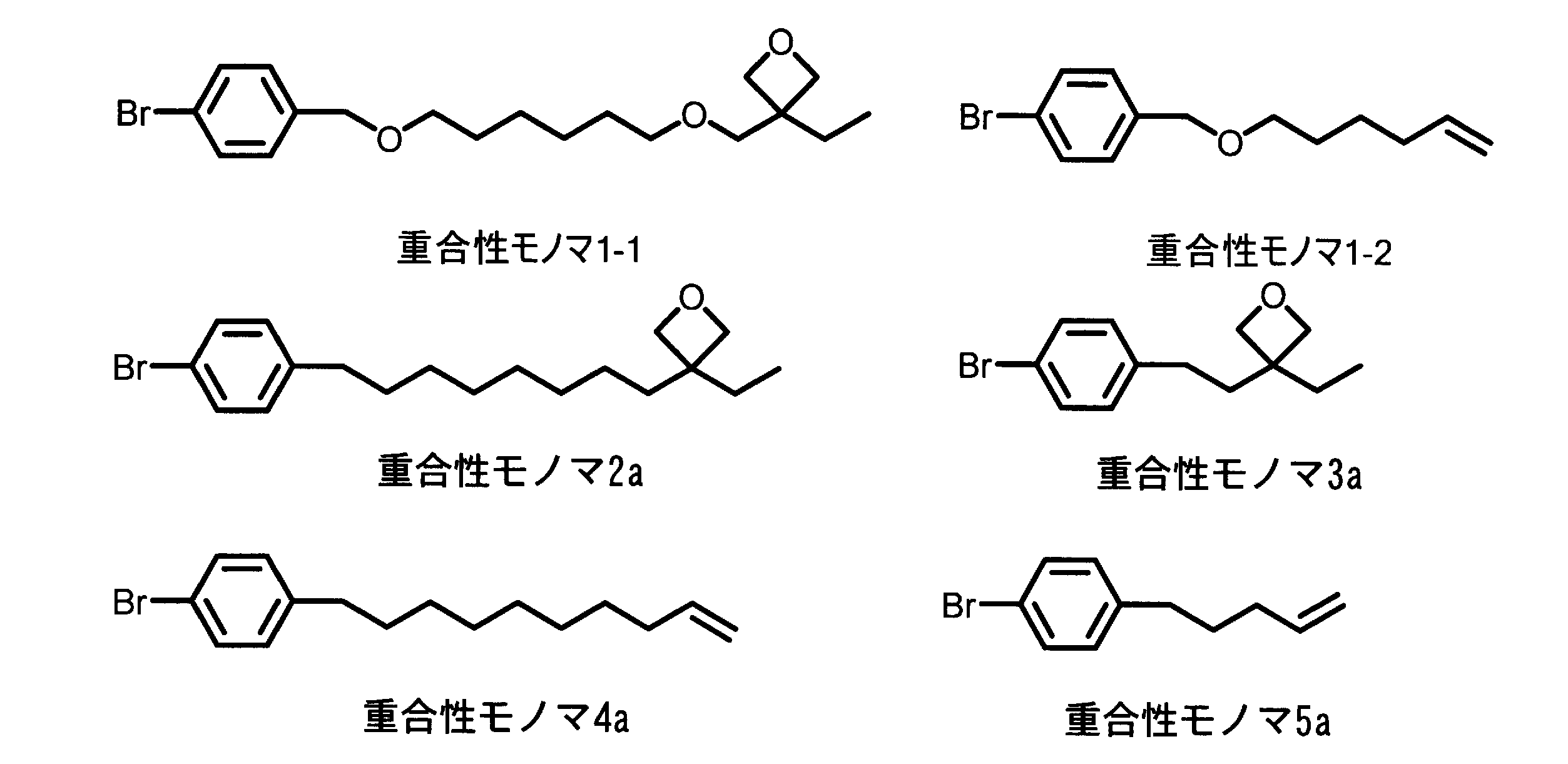


表6の比較例1a~14a、及び実施例1a~32aに示す有機EL素子を次の手順で作製した。
ITOを1.6mm幅にパターンニングしたガラス基板上に、PEDOT:PSS分散液(シュタルク・ヴィテック社製、AI4083 LVW142)を、回転速度1500min-1でスピン塗布し、ホットプレート上で空気中、200℃/10分加熱乾燥して、正孔注入層(40nm)を形成した。以後の実験は乾燥窒素環境下で行った。


2 陽極
3 正孔注入層
4 陰極
5 電子注入層
6 正孔輸送層
7 電子輸送層
8 基板
Claims (20)
- 下記式(1)、下記式(2)、及び下記式(3)からなる群から選択される少なくとも1つの構造を含む電荷輸送性ポリマーを含有する有機エレクトロニクス材料。

- 前記電荷輸送性ポリマーが、前記(1)、式(2)、及び式(3)からなる群から選択される少なくとも1つの構造を末端に有する、請求項1に記載の有機エレクトロニクス材料。
- 下記式(1a)、下記式(2a)、及び下記式(3a)からなる群から選択される少なくとも1つの構造を含む電荷輸送性ポリマーを含有する有機エレクトロニクス材料。

- 前記電荷輸送性ポリマーが、前記(1a)、式(2a)、及び式(3a)からなる群から選択される少なくとも1つの構造を末端に有する、請求項3に記載の有機エレクトロニクス材料。
- 前記電荷輸送性ポリマーが、3方向以上に分岐した構造を有する電荷輸送性ポリマーであって、置換又は非置換の、芳香族アミン構造、カルバゾール構造、チオフェン構造、ビチオフェン構造、ベンゼン構造、複数のベンゼン環が縮合した多環芳香族構造、及びフルオレン構造からなる群から選択される構造を含む3価以上の構造単位を含む、請求項1~4のいずれか1項に記載の有機エレクトロニクス材料。
- 前記電荷輸送性ポリマーが、置換又は非置換の、芳香族アミン構造、カルバゾール構造、チオフェン構造、ビチオフェン構造、ベンゼン構造、複数のベンゼン環が縮合した多環芳香族構造、及びフルオレン構造からなる群から選択される構造を含む2価の構造単位を含む、請求項1~5のいずれか一項に記載の有機エレクトロニクス材料。
- 前記電荷輸送性ポリマーが正孔輸送材料である、請求項1~6のいずれか一項に記載の有機エレクトロニクス材料。
- さらに重合開始剤を含む、請求項1~7のいずれか一項に記載の有機エレクトロニクス材料。
- 前記重合開始剤がカチオン重合開始剤を含む、請求項8に記載の有機エレクトロニクス材料。
- 前記カチオン重合開始剤がオニウム塩を含む、請求項9に記載の有機エレクトロニクス材料。
- 請求項1~10のいずれか一項に記載の有機エレクトロニクス材料により形成された、有機層。
- 請求項11に記載の有機層を含む、有機エレクトロニクス素子。
- 請求項11に記載の有機層を含む、有機エレクトロルミネセンス素子。
- 燐光材料を含む発光層を有する、請求項13に記載の有機エレクトロルミネセンス素子。
- 遅延蛍光材料を含む発光層を有する、請求項13に記載の有機エレクトロルミネセンス素子。
- フレキシブル基板をさらに有する、請求項13~15のいずれか一項に記載の有機エレクトロルミネセンス素子。
- 樹脂フィルム基板をさらに有する、請求項13~15のいずれか一項に記載の有機エレクトロルミネセンス素子。
- 請求項13~17のいずれか一項に記載の有機エレクトロルミネセンス素子を備えた、表示素子。
- 請求項13~17のいずれか一項に記載の有機エレクトロルミネセンス素子を備えた、照明装置。
- 請求項19に記載の照明装置と、表示手段として液晶素子とを備えた、表示装置。
Priority Applications (5)
| Application Number | Priority Date | Filing Date | Title |
|---|---|---|---|
| JP2018529820A JP7044063B2 (ja) | 2016-07-25 | 2017-07-20 | 有機エレクトロニクス材料及びその利用 |
| EP17834141.8A EP3489276A4 (en) | 2016-07-25 | 2017-07-20 | ORGANIC ELECTRONIC MATERIAL AND USE THEREOF |
| US16/320,358 US20190267550A1 (en) | 2016-07-25 | 2017-07-20 | Organic electronic material and use of same |
| KR1020187036955A KR20190032292A (ko) | 2016-07-25 | 2017-07-20 | 유기 전자 재료 및 그 이용 |
| CN201780042878.3A CN109476827A (zh) | 2016-07-25 | 2017-07-20 | 有机电子材料及其利用 |
Applications Claiming Priority (4)
| Application Number | Priority Date | Filing Date | Title |
|---|---|---|---|
| JP2016-145263 | 2016-07-25 | ||
| JP2016145263 | 2016-07-25 | ||
| JP2016217367 | 2016-11-07 | ||
| JP2016-217367 | 2016-11-07 |
Publications (1)
| Publication Number | Publication Date |
|---|---|
| WO2018021133A1 true WO2018021133A1 (ja) | 2018-02-01 |
Family
ID=61016163
Family Applications (1)
| Application Number | Title | Priority Date | Filing Date |
|---|---|---|---|
| PCT/JP2017/026222 WO2018021133A1 (ja) | 2016-07-25 | 2017-07-20 | 有機エレクトロニクス材料及びその利用 |
Country Status (7)
| Country | Link |
|---|---|
| US (1) | US20190267550A1 (ja) |
| EP (1) | EP3489276A4 (ja) |
| JP (1) | JP7044063B2 (ja) |
| KR (1) | KR20190032292A (ja) |
| CN (1) | CN109476827A (ja) |
| TW (1) | TW201823422A (ja) |
| WO (1) | WO2018021133A1 (ja) |
Cited By (5)
| Publication number | Priority date | Publication date | Assignee | Title |
|---|---|---|---|---|
| JP2018061028A (ja) * | 2016-09-29 | 2018-04-12 | 住友化学株式会社 | 発光素子 |
| JP2018061030A (ja) * | 2016-09-29 | 2018-04-12 | 住友化学株式会社 | 発光素子 |
| WO2020012601A1 (ja) * | 2018-07-12 | 2020-01-16 | 日立化成株式会社 | 電荷輸送性ポリマー及び有機エレクトロニクス素子 |
| WO2020217520A1 (ja) * | 2019-04-26 | 2020-10-29 | 日立化成株式会社 | 有機エレクトロニクス材料及び電荷輸送性ポリマーの製造方法 |
| KR20210056367A (ko) * | 2018-09-28 | 2021-05-18 | 쇼와덴코머티리얼즈가부시끼가이샤 | 유기 일렉트로닉스 재료 및 유기 일렉트로닉스 소자 |
Families Citing this family (1)
| Publication number | Priority date | Publication date | Assignee | Title |
|---|---|---|---|---|
| CN115058030B (zh) * | 2022-07-12 | 2024-07-09 | 中南大学 | 一种多形态各向异性半导体聚合物纳米结构的制备方法 |
Citations (10)
| Publication number | Priority date | Publication date | Assignee | Title |
|---|---|---|---|---|
| JP2009283509A (ja) * | 2008-05-19 | 2009-12-03 | Nippon Hoso Kyokai <Nhk> | 有機el素子および有機elディスプレイ |
| JP2010118653A (ja) * | 2008-10-16 | 2010-05-27 | Hitachi Chem Co Ltd | 有機エレクトロニクス用材料、この材料を用いた有機エレクトロニクス素子及び有機エレクトロルミネセンス素子、並びに表示装置、照明装置、表示素子 |
| JP2013036023A (ja) * | 2011-07-13 | 2013-02-21 | Toyo Ink Sc Holdings Co Ltd | 有機エレクトロルミネッセンス素子用材料およびその用途 |
| JP2013045986A (ja) * | 2011-08-26 | 2013-03-04 | Toyo Ink Sc Holdings Co Ltd | 有機エレクトロルミネッセンス素子用材料およびその用途 |
| JP2013124271A (ja) * | 2011-12-14 | 2013-06-24 | Toyo Ink Sc Holdings Co Ltd | 有機エレクトロルミネッセンス素子用材料およびその用途 |
| JP2013209300A (ja) * | 2012-03-30 | 2013-10-10 | Toyo Ink Sc Holdings Co Ltd | 有機エレクトロルミネッセンス素子用材料およびその用途 |
| JP2014019755A (ja) * | 2012-07-13 | 2014-02-03 | Hitachi Chemical Co Ltd | 硬化性重合体並びにこれを用いた樹脂及び有機el素子 |
| JP2014192291A (ja) * | 2013-03-27 | 2014-10-06 | Hitachi Chemical Co Ltd | 重合性塗布液並びにこれを用いて形成した樹脂及び有機エレクトロルミネッセンス素子並びに重合性塗布液及び有機エレクトロルミネッセンス素子の製造方法 |
| JP2015017231A (ja) * | 2013-07-12 | 2015-01-29 | 凸版印刷株式会社 | 電荷輸送ポリマー、ならびにそれを用いた電荷輸送ポリマー組成物、発光性電荷輸送膜および有機el素子 |
| JP2015126115A (ja) * | 2013-12-26 | 2015-07-06 | 日立化成株式会社 | 電荷輸送性材料、該材料を用いたインク組成物、有機エレクトロニクス素子、有機エレクトロルミネセンス素子、表示素子、表示装置及び照明装置 |
Family Cites Families (7)
| Publication number | Priority date | Publication date | Assignee | Title |
|---|---|---|---|---|
| JP2006279007A (ja) | 2005-03-02 | 2006-10-12 | Konica Minolta Holdings Inc | 有機エレクトロルミネッセンス素子、表示装置及び照明装置 |
| JP5625271B2 (ja) * | 2008-07-29 | 2014-11-19 | 住友化学株式会社 | 高分子化合物及びそれを用いた発光素子 |
| JP5491796B2 (ja) * | 2008-08-11 | 2014-05-14 | 三菱化学株式会社 | 電荷輸送性ポリマー、有機電界発光素子用組成物、有機電界発光素子、有機elディスプレイ及び有機el照明 |
| EP2439804B1 (en) * | 2009-06-01 | 2021-07-21 | Showa Denko Materials Co., Ltd. | Organic electronic material, ink composition containing same, and organic thin film, organic electronic element, organic electroluminescent element, lighting device, and display device formed therewith |
| JP5351231B2 (ja) | 2011-10-04 | 2013-11-27 | アンリツ株式会社 | リレーノードシミュレーター及び試験方法 |
| JP6613561B2 (ja) | 2014-12-12 | 2019-12-04 | 日立化成株式会社 | 有機エレクトロニクス材料及び有機エレクトロニクス素子 |
| WO2017188023A1 (ja) * | 2016-04-28 | 2017-11-02 | 日立化成株式会社 | 電荷輸送性材料及びその利用 |
-
2017
- 2017-07-20 US US16/320,358 patent/US20190267550A1/en not_active Abandoned
- 2017-07-20 CN CN201780042878.3A patent/CN109476827A/zh active Pending
- 2017-07-20 EP EP17834141.8A patent/EP3489276A4/en not_active Withdrawn
- 2017-07-20 JP JP2018529820A patent/JP7044063B2/ja active Active
- 2017-07-20 WO PCT/JP2017/026222 patent/WO2018021133A1/ja unknown
- 2017-07-20 KR KR1020187036955A patent/KR20190032292A/ko unknown
- 2017-07-24 TW TW106124706A patent/TW201823422A/zh unknown
Patent Citations (10)
| Publication number | Priority date | Publication date | Assignee | Title |
|---|---|---|---|---|
| JP2009283509A (ja) * | 2008-05-19 | 2009-12-03 | Nippon Hoso Kyokai <Nhk> | 有機el素子および有機elディスプレイ |
| JP2010118653A (ja) * | 2008-10-16 | 2010-05-27 | Hitachi Chem Co Ltd | 有機エレクトロニクス用材料、この材料を用いた有機エレクトロニクス素子及び有機エレクトロルミネセンス素子、並びに表示装置、照明装置、表示素子 |
| JP2013036023A (ja) * | 2011-07-13 | 2013-02-21 | Toyo Ink Sc Holdings Co Ltd | 有機エレクトロルミネッセンス素子用材料およびその用途 |
| JP2013045986A (ja) * | 2011-08-26 | 2013-03-04 | Toyo Ink Sc Holdings Co Ltd | 有機エレクトロルミネッセンス素子用材料およびその用途 |
| JP2013124271A (ja) * | 2011-12-14 | 2013-06-24 | Toyo Ink Sc Holdings Co Ltd | 有機エレクトロルミネッセンス素子用材料およびその用途 |
| JP2013209300A (ja) * | 2012-03-30 | 2013-10-10 | Toyo Ink Sc Holdings Co Ltd | 有機エレクトロルミネッセンス素子用材料およびその用途 |
| JP2014019755A (ja) * | 2012-07-13 | 2014-02-03 | Hitachi Chemical Co Ltd | 硬化性重合体並びにこれを用いた樹脂及び有機el素子 |
| JP2014192291A (ja) * | 2013-03-27 | 2014-10-06 | Hitachi Chemical Co Ltd | 重合性塗布液並びにこれを用いて形成した樹脂及び有機エレクトロルミネッセンス素子並びに重合性塗布液及び有機エレクトロルミネッセンス素子の製造方法 |
| JP2015017231A (ja) * | 2013-07-12 | 2015-01-29 | 凸版印刷株式会社 | 電荷輸送ポリマー、ならびにそれを用いた電荷輸送ポリマー組成物、発光性電荷輸送膜および有機el素子 |
| JP2015126115A (ja) * | 2013-12-26 | 2015-07-06 | 日立化成株式会社 | 電荷輸送性材料、該材料を用いたインク組成物、有機エレクトロニクス素子、有機エレクトロルミネセンス素子、表示素子、表示装置及び照明装置 |
Non-Patent Citations (1)
| Title |
|---|
| See also references of EP3489276A4 * |
Cited By (11)
| Publication number | Priority date | Publication date | Assignee | Title |
|---|---|---|---|---|
| JP2018061028A (ja) * | 2016-09-29 | 2018-04-12 | 住友化学株式会社 | 発光素子 |
| JP2018061030A (ja) * | 2016-09-29 | 2018-04-12 | 住友化学株式会社 | 発光素子 |
| WO2020012601A1 (ja) * | 2018-07-12 | 2020-01-16 | 日立化成株式会社 | 電荷輸送性ポリマー及び有機エレクトロニクス素子 |
| JPWO2020012601A1 (ja) * | 2018-07-12 | 2021-08-26 | 昭和電工マテリアルズ株式会社 | 電荷輸送性ポリマー及び有機エレクトロニクス素子 |
| TWI810330B (zh) * | 2018-07-12 | 2023-08-01 | 日商力森諾科股份有限公司 | 電荷輸送性聚合物、電荷輸送性材料、油墨組成物、有機層、有機電子元件、有機電致發光元件、顯示元件、照明裝置、顯示裝置 |
| JP7363784B2 (ja) | 2018-07-12 | 2023-10-18 | 株式会社レゾナック | 電荷輸送性ポリマー及び有機エレクトロニクス素子 |
| KR20210056367A (ko) * | 2018-09-28 | 2021-05-18 | 쇼와덴코머티리얼즈가부시끼가이샤 | 유기 일렉트로닉스 재료 및 유기 일렉트로닉스 소자 |
| KR102537755B1 (ko) * | 2018-09-28 | 2023-05-26 | 가부시끼가이샤 레조낙 | 유기 일렉트로닉스 재료 및 유기 일렉트로닉스 소자 |
| WO2020217520A1 (ja) * | 2019-04-26 | 2020-10-29 | 日立化成株式会社 | 有機エレクトロニクス材料及び電荷輸送性ポリマーの製造方法 |
| JPWO2020217520A1 (ja) * | 2019-04-26 | 2020-10-29 | ||
| JP7416058B2 (ja) | 2019-04-26 | 2024-01-17 | 株式会社レゾナック | 有機エレクトロニクス材料及び電荷輸送性ポリマーの製造方法 |
Also Published As
| Publication number | Publication date |
|---|---|
| US20190267550A1 (en) | 2019-08-29 |
| EP3489276A4 (en) | 2020-03-18 |
| JPWO2018021133A1 (ja) | 2019-06-13 |
| TW201823422A (zh) | 2018-07-01 |
| EP3489276A1 (en) | 2019-05-29 |
| JP7044063B2 (ja) | 2022-03-30 |
| CN109476827A (zh) | 2019-03-15 |
| KR20190032292A (ko) | 2019-03-27 |
Similar Documents
| Publication | Publication Date | Title |
|---|---|---|
| WO2018021133A1 (ja) | 有機エレクトロニクス材料及びその利用 | |
| JP7425418B2 (ja) | 電荷輸送性材料、有機エレクトロニクス素子、及び有機エレクトロルミネセンス素子 | |
| JP2017069324A (ja) | 有機エレクトロニクス材料、有機層、有機エレクトロニクス素子、有機エレクトロルミネセンス素子、表示素子、照明装置、及び表示素子 | |
| WO2017043502A1 (ja) | 有機エレクトロニクス材料及びその利用 | |
| WO2018143438A1 (ja) | 有機エレクトロニクス材料及びその利用 | |
| JP2017123438A (ja) | 有機エレクトロニクス材料、有機エレクトロニクス素子、及び有機エレクトロルミネセンス素子 | |
| WO2018146779A1 (ja) | 有機エレクトロニクス材料、有機エレクトロニクス素子、及び有機エレクトロルミネセンス素子 | |
| WO2018159694A1 (ja) | 有機エレクトロニクス材料及びその利用 | |
| WO2018021381A1 (ja) | 有機エレクトロニクス材料 | |
| WO2017179661A1 (ja) | 電荷輸送性材料、該材料を用いたインク組成物、有機エレクトロニクス素子、有機エレクトロルミネセンス素子、表示素子、照明装置、及び表示装置 | |
| JP6641845B2 (ja) | 電荷輸送性材料、該材料を用いたインキ組成物、有機エレクトロニクス素子、有機エレクトロルミネセンス素子、表示素子、照明装置、及び表示装置 | |
| WO2018020571A1 (ja) | 有機エレクトロニクス材料 | |
| JP2017069385A (ja) | 電荷輸送性材料、該材料を用いたインク組成物、有機エレクトロニクス素子、有機エレクトロルミネセンス素子、表示素子、照明装置、及び表示装置 | |
| JP6816540B2 (ja) | 電荷輸送性材料、該材料を用いたインク組成物、有機エレクトロニクス素子、有機エレクトロルミネセンス素子、表示素子、照明装置、及び表示装置 | |
| WO2020065926A1 (ja) | 有機エレクトロニクス材料及びその利用 | |
| JP2017050338A (ja) | 有機エレクトロニクス材料及び有機エレクトロニクス素子 | |
| JP6657702B2 (ja) | 有機エレクトロニクス材料及び該材料を含むインク組成物、並びに有機エレクトロニクス素子及び有機エレクトロルミネセンス素子 | |
| WO2019009327A1 (ja) | 有機エレクトロニクス材料及び有機エレクトロニクス素子 | |
| JP2017199866A (ja) | 電荷輸送性材料及びその利用 | |
| WO2020067300A1 (ja) | 有機エレクトロニクス材料及び有機エレクトロニクス素子 | |
| JP6657663B2 (ja) | 電荷輸送性材料、該材料を用いたインク組成物、有機エレクトロニクス素子、有機エレクトロルミネセンス素子、表示素子、表示装置及び照明装置 | |
| WO2019175976A1 (ja) | 有機エレクトロニクス材料及び有機エレクトロニクス素子 | |
| JP2017059718A (ja) | 有機エレクトロニクス材料及び該材料を含むインク組成物、並びに有機エレクトロニクス素子及び有機エレクトロルミネセンス素子 | |
| WO2020065920A1 (ja) | 有機エレクトロニクス材料及び有機エレクトロニクス素子 | |
| JP6690241B2 (ja) | 有機エレクトロニクス材料及びその利用 |
Legal Events
| Date | Code | Title | Description |
|---|---|---|---|
| 121 | Ep: the epo has been informed by wipo that ep was designated in this application |
Ref document number: 17834141 Country of ref document: EP Kind code of ref document: A1 |
|
| ENP | Entry into the national phase |
Ref document number: 2018529820 Country of ref document: JP Kind code of ref document: A |
|
| ENP | Entry into the national phase |
Ref document number: 20187036955 Country of ref document: KR Kind code of ref document: A |
|
| NENP | Non-entry into the national phase |
Ref country code: DE |
|
| ENP | Entry into the national phase |
Ref document number: 2017834141 Country of ref document: EP Effective date: 20190225 |