WO2018016257A1 - 基板処理装置 - Google Patents
基板処理装置 Download PDFInfo
- Publication number
- WO2018016257A1 WO2018016257A1 PCT/JP2017/022866 JP2017022866W WO2018016257A1 WO 2018016257 A1 WO2018016257 A1 WO 2018016257A1 JP 2017022866 W JP2017022866 W JP 2017022866W WO 2018016257 A1 WO2018016257 A1 WO 2018016257A1
- Authority
- WO
- WIPO (PCT)
- Prior art keywords
- substrate
- processing
- mounting
- wafer
- processing apparatus
- Prior art date
Links
Images


Classifications
-
- H—ELECTRICITY
- H01—ELECTRIC ELEMENTS
- H01L—SEMICONDUCTOR DEVICES NOT COVERED BY CLASS H10
- H01L21/00—Processes or apparatus adapted for the manufacture or treatment of semiconductor or solid state devices or of parts thereof
- H01L21/67—Apparatus specially adapted for handling semiconductor or electric solid state devices during manufacture or treatment thereof; Apparatus specially adapted for handling wafers during manufacture or treatment of semiconductor or electric solid state devices or components ; Apparatus not specifically provided for elsewhere
- H01L21/677—Apparatus specially adapted for handling semiconductor or electric solid state devices during manufacture or treatment thereof; Apparatus specially adapted for handling wafers during manufacture or treatment of semiconductor or electric solid state devices or components ; Apparatus not specifically provided for elsewhere for conveying, e.g. between different workstations
- H01L21/67703—Apparatus specially adapted for handling semiconductor or electric solid state devices during manufacture or treatment thereof; Apparatus specially adapted for handling wafers during manufacture or treatment of semiconductor or electric solid state devices or components ; Apparatus not specifically provided for elsewhere for conveying, e.g. between different workstations between different workstations
- H01L21/6773—Conveying cassettes, containers or carriers
-
- B—PERFORMING OPERATIONS; TRANSPORTING
- B65—CONVEYING; PACKING; STORING; HANDLING THIN OR FILAMENTARY MATERIAL
- B65G—TRANSPORT OR STORAGE DEVICES, e.g. CONVEYORS FOR LOADING OR TIPPING, SHOP CONVEYOR SYSTEMS OR PNEUMATIC TUBE CONVEYORS
- B65G49/00—Conveying systems characterised by their application for specified purposes not otherwise provided for
- B65G49/05—Conveying systems characterised by their application for specified purposes not otherwise provided for for fragile or damageable materials or articles
- B65G49/07—Conveying systems characterised by their application for specified purposes not otherwise provided for for fragile or damageable materials or articles for semiconductor wafers Not used, see H01L21/677
-
- B—PERFORMING OPERATIONS; TRANSPORTING
- B65—CONVEYING; PACKING; STORING; HANDLING THIN OR FILAMENTARY MATERIAL
- B65G—TRANSPORT OR STORAGE DEVICES, e.g. CONVEYORS FOR LOADING OR TIPPING, SHOP CONVEYOR SYSTEMS OR PNEUMATIC TUBE CONVEYORS
- B65G49/00—Conveying systems characterised by their application for specified purposes not otherwise provided for
- B65G49/05—Conveying systems characterised by their application for specified purposes not otherwise provided for for fragile or damageable materials or articles
- B65G49/06—Conveying systems characterised by their application for specified purposes not otherwise provided for for fragile or damageable materials or articles for fragile sheets, e.g. glass
- B65G49/061—Lifting, gripping, or carrying means, for one or more sheets forming independent means of transport, e.g. suction cups, transport frames
-
- H—ELECTRICITY
- H01—ELECTRIC ELEMENTS
- H01L—SEMICONDUCTOR DEVICES NOT COVERED BY CLASS H10
- H01L21/00—Processes or apparatus adapted for the manufacture or treatment of semiconductor or solid state devices or of parts thereof
- H01L21/67—Apparatus specially adapted for handling semiconductor or electric solid state devices during manufacture or treatment thereof; Apparatus specially adapted for handling wafers during manufacture or treatment of semiconductor or electric solid state devices or components ; Apparatus not specifically provided for elsewhere
- H01L21/67005—Apparatus not specifically provided for elsewhere
- H01L21/67011—Apparatus for manufacture or treatment
- H01L21/67155—Apparatus for manufacturing or treating in a plurality of work-stations
- H01L21/67161—Apparatus for manufacturing or treating in a plurality of work-stations characterized by the layout of the process chambers
- H01L21/67173—Apparatus for manufacturing or treating in a plurality of work-stations characterized by the layout of the process chambers in-line arrangement
-
- H—ELECTRICITY
- H01—ELECTRIC ELEMENTS
- H01L—SEMICONDUCTOR DEVICES NOT COVERED BY CLASS H10
- H01L21/00—Processes or apparatus adapted for the manufacture or treatment of semiconductor or solid state devices or of parts thereof
- H01L21/67—Apparatus specially adapted for handling semiconductor or electric solid state devices during manufacture or treatment thereof; Apparatus specially adapted for handling wafers during manufacture or treatment of semiconductor or electric solid state devices or components ; Apparatus not specifically provided for elsewhere
- H01L21/67005—Apparatus not specifically provided for elsewhere
- H01L21/67011—Apparatus for manufacture or treatment
- H01L21/67155—Apparatus for manufacturing or treating in a plurality of work-stations
- H01L21/67161—Apparatus for manufacturing or treating in a plurality of work-stations characterized by the layout of the process chambers
- H01L21/67178—Apparatus for manufacturing or treating in a plurality of work-stations characterized by the layout of the process chambers vertical arrangement
-
- H—ELECTRICITY
- H01—ELECTRIC ELEMENTS
- H01L—SEMICONDUCTOR DEVICES NOT COVERED BY CLASS H10
- H01L21/00—Processes or apparatus adapted for the manufacture or treatment of semiconductor or solid state devices or of parts thereof
- H01L21/67—Apparatus specially adapted for handling semiconductor or electric solid state devices during manufacture or treatment thereof; Apparatus specially adapted for handling wafers during manufacture or treatment of semiconductor or electric solid state devices or components ; Apparatus not specifically provided for elsewhere
- H01L21/67005—Apparatus not specifically provided for elsewhere
- H01L21/67011—Apparatus for manufacture or treatment
- H01L21/67155—Apparatus for manufacturing or treating in a plurality of work-stations
- H01L21/67201—Apparatus for manufacturing or treating in a plurality of work-stations characterized by the construction of the load-lock chamber
-
- H—ELECTRICITY
- H01—ELECTRIC ELEMENTS
- H01L—SEMICONDUCTOR DEVICES NOT COVERED BY CLASS H10
- H01L21/00—Processes or apparatus adapted for the manufacture or treatment of semiconductor or solid state devices or of parts thereof
- H01L21/67—Apparatus specially adapted for handling semiconductor or electric solid state devices during manufacture or treatment thereof; Apparatus specially adapted for handling wafers during manufacture or treatment of semiconductor or electric solid state devices or components ; Apparatus not specifically provided for elsewhere
- H01L21/677—Apparatus specially adapted for handling semiconductor or electric solid state devices during manufacture or treatment thereof; Apparatus specially adapted for handling wafers during manufacture or treatment of semiconductor or electric solid state devices or components ; Apparatus not specifically provided for elsewhere for conveying, e.g. between different workstations
- H01L21/67739—Apparatus specially adapted for handling semiconductor or electric solid state devices during manufacture or treatment thereof; Apparatus specially adapted for handling wafers during manufacture or treatment of semiconductor or electric solid state devices or components ; Apparatus not specifically provided for elsewhere for conveying, e.g. between different workstations into and out of processing chamber
- H01L21/67742—Mechanical parts of transfer devices
-
- H—ELECTRICITY
- H01—ELECTRIC ELEMENTS
- H01L—SEMICONDUCTOR DEVICES NOT COVERED BY CLASS H10
- H01L21/00—Processes or apparatus adapted for the manufacture or treatment of semiconductor or solid state devices or of parts thereof
- H01L21/67—Apparatus specially adapted for handling semiconductor or electric solid state devices during manufacture or treatment thereof; Apparatus specially adapted for handling wafers during manufacture or treatment of semiconductor or electric solid state devices or components ; Apparatus not specifically provided for elsewhere
- H01L21/677—Apparatus specially adapted for handling semiconductor or electric solid state devices during manufacture or treatment thereof; Apparatus specially adapted for handling wafers during manufacture or treatment of semiconductor or electric solid state devices or components ; Apparatus not specifically provided for elsewhere for conveying, e.g. between different workstations
- H01L21/67739—Apparatus specially adapted for handling semiconductor or electric solid state devices during manufacture or treatment thereof; Apparatus specially adapted for handling wafers during manufacture or treatment of semiconductor or electric solid state devices or components ; Apparatus not specifically provided for elsewhere for conveying, e.g. between different workstations into and out of processing chamber
- H01L21/67757—Apparatus specially adapted for handling semiconductor or electric solid state devices during manufacture or treatment thereof; Apparatus specially adapted for handling wafers during manufacture or treatment of semiconductor or electric solid state devices or components ; Apparatus not specifically provided for elsewhere for conveying, e.g. between different workstations into and out of processing chamber vertical transfer of a batch of workpieces
-
- H—ELECTRICITY
- H01—ELECTRIC ELEMENTS
- H01L—SEMICONDUCTOR DEVICES NOT COVERED BY CLASS H10
- H01L21/00—Processes or apparatus adapted for the manufacture or treatment of semiconductor or solid state devices or of parts thereof
- H01L21/67—Apparatus specially adapted for handling semiconductor or electric solid state devices during manufacture or treatment thereof; Apparatus specially adapted for handling wafers during manufacture or treatment of semiconductor or electric solid state devices or components ; Apparatus not specifically provided for elsewhere
- H01L21/677—Apparatus specially adapted for handling semiconductor or electric solid state devices during manufacture or treatment thereof; Apparatus specially adapted for handling wafers during manufacture or treatment of semiconductor or electric solid state devices or components ; Apparatus not specifically provided for elsewhere for conveying, e.g. between different workstations
- H01L21/67763—Apparatus specially adapted for handling semiconductor or electric solid state devices during manufacture or treatment thereof; Apparatus specially adapted for handling wafers during manufacture or treatment of semiconductor or electric solid state devices or components ; Apparatus not specifically provided for elsewhere for conveying, e.g. between different workstations the wafers being stored in a carrier, involving loading and unloading
- H01L21/67775—Docking arrangements
-
- H—ELECTRICITY
- H01—ELECTRIC ELEMENTS
- H01L—SEMICONDUCTOR DEVICES NOT COVERED BY CLASS H10
- H01L21/00—Processes or apparatus adapted for the manufacture or treatment of semiconductor or solid state devices or of parts thereof
- H01L21/67—Apparatus specially adapted for handling semiconductor or electric solid state devices during manufacture or treatment thereof; Apparatus specially adapted for handling wafers during manufacture or treatment of semiconductor or electric solid state devices or components ; Apparatus not specifically provided for elsewhere
- H01L21/677—Apparatus specially adapted for handling semiconductor or electric solid state devices during manufacture or treatment thereof; Apparatus specially adapted for handling wafers during manufacture or treatment of semiconductor or electric solid state devices or components ; Apparatus not specifically provided for elsewhere for conveying, e.g. between different workstations
- H01L21/67763—Apparatus specially adapted for handling semiconductor or electric solid state devices during manufacture or treatment thereof; Apparatus specially adapted for handling wafers during manufacture or treatment of semiconductor or electric solid state devices or components ; Apparatus not specifically provided for elsewhere for conveying, e.g. between different workstations the wafers being stored in a carrier, involving loading and unloading
- H01L21/67778—Apparatus specially adapted for handling semiconductor or electric solid state devices during manufacture or treatment thereof; Apparatus specially adapted for handling wafers during manufacture or treatment of semiconductor or electric solid state devices or components ; Apparatus not specifically provided for elsewhere for conveying, e.g. between different workstations the wafers being stored in a carrier, involving loading and unloading involving loading and unloading of wafers
-
- B—PERFORMING OPERATIONS; TRANSPORTING
- B65—CONVEYING; PACKING; STORING; HANDLING THIN OR FILAMENTARY MATERIAL
- B65G—TRANSPORT OR STORAGE DEVICES, e.g. CONVEYORS FOR LOADING OR TIPPING, SHOP CONVEYOR SYSTEMS OR PNEUMATIC TUBE CONVEYORS
- B65G2201/00—Indexing codes relating to handling devices, e.g. conveyors, characterised by the type of product or load being conveyed or handled
- B65G2201/02—Articles
- B65G2201/0214—Articles of special size, shape or weigh
- B65G2201/022—Flat
Definitions
- the present invention relates to a substrate processing apparatus including an EFEM (Equipment Front End Module) for taking out a substrate from a substrate transfer container and a processing module for processing the substrate.
- EFEM Equipment Front End Module
- vacuum processing such as film formation, etching, ashing, and annealing is performed on a semiconductor wafer (hereinafter referred to as “wafer”).
- wafer a semiconductor wafer
- this is called a multi-chamber system in which a polygonal vacuum transfer chamber is connected to EFEM via a load lock chamber, and a vacuum processing module is connected to one side of this vacuum transfer chamber.
- Vacuum processing systems are known.
- Patent Document 1 an apparatus front-end module (EFEM) for pulling out a wafer from a wafer carrier, a linear robot that moves a wafer along an elongated path, and two vacuum processes provided on both sides of the linear robot are provided.
- EFEM apparatus front-end module
- a system comprising a processing cluster for performing is described.
- the processing cluster includes a cluster robot that transfers wafers between the first and second processing chambers and the linear robot.
- Patent Document 1 describes that a linear robot may operate at atmospheric pressure and can be configured by a wafer shuttle.
- Patent Document 2 and Patent Document 3 also describe a layout in which a plurality of apparatuses for performing vacuum processing are arranged on both sides of a linear guide path for placing and transporting a wafer.
- These conventional techniques can increase the number of processing chambers mounted as compared to a multi-chamber system, and are expected to contribute to an improvement in throughput.
- JP 2014-68009 A (FIG. 4, paragraph 0037, FIG. 5, paragraph 0039 and paragraph 0042) JP 2004-349503 A (FIG. 4) JP 2003-188229 A (FIGS. 1 and 2)
- the present invention has been made under such circumstances, and an object of the present invention is to provide a technique capable of improving throughput while suppressing an increase in apparatus cost when processing a substrate.
- the substrate processing apparatus of the present invention comprises: An EFEM including a container placement portion for placing a transport container storing a plurality of substrates, and a delivery mechanism for delivering the substrate to the transport container placed on the container placement portion; A moving part provided movably along a moving path extending linearly toward the back side as viewed from the EFEM; A plurality of processing units that are provided so as to face the moving path when viewed in a plane and are arranged one above the other, A substrate mounting section provided on the moving section so as to be movable up and down via an elevating mechanism, and configured so that a plurality of substrates can be mounted in a shelf shape,
- the processing unit includes a processing module for processing a substrate, and a substrate transport mechanism for transferring the substrate between the processing module and the substrate platform,
- the substrate mounting portion is configured to be movable between a position where the substrate is transferred by the transfer mechanism and a position where the substrate is transferred by the substrate transfer mechanism of each of the plurality of processing units. It is characterized by
- the present invention relates to a substrate processing apparatus including an EFEM and a processing module for processing a substrate, and includes a plurality of processing units each including a processing module and a substrate transport mechanism so as to face a moving path extending from the back when viewed from the EFEM. It is arranged. Then, a substrate mounting section capable of storing a plurality of substrates in a shelf shape is provided so as to be movable and movable up and down along the above movement path, and transport between the substrate transfer mechanism on the EFEM side and the substrate transport mechanism on the processing unit side. Is held by the substrate mounting portion. For this reason, a high throughput can be obtained, and an increase in cost regarding the mechanism for conveyance can be suppressed.
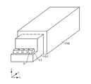
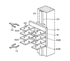
- 1 is an external view showing a substrate processing apparatus according to a first embodiment of the present invention.
- 1 is a plan view showing a substrate processing apparatus according to a first embodiment. It is a perspective view which shows the inside of the substrate processing apparatus which concerns on 1st Embodiment. It is a side view which shows the inside of the substrate processing apparatus which concerns on 1st Embodiment. It is a disassembled perspective view which shows the board
- a substrate processing apparatus will be described. As shown in the external view of FIG. 1, this substrate processing apparatus is connected to the EFEM 101 for taking out a wafer from a carrier C, which is a transfer container containing a plurality of wafers as a substrate, and processes the wafer. And a processing block 102.
- the EFEM 101 includes a load port 11 that is a container mounting portion configured such that, for example, four carriers C that are FOUPs are mounted, for example, in the left-right direction (X direction).
- the support part 10 which supports in the state which positioned the bottom part of the carrier C is shown.
- a transfer chamber 13 in which a transfer mechanism 12 for transferring a wafer to the carrier C is disposed is provided.
- the transfer chamber 13 is set to a normal pressure atmosphere, for example, an air atmosphere, and an opening / closing door 14 that opens and closes an opening serving as a wafer take-out port is provided on a wall portion facing the carrier C in the transfer chamber 13.
- the delivery mechanism 12 includes a base arm (not shown) that is movable along a guide 15 (see FIG. 2) extending in the X direction, and a telescopic joint arm that is movable up and down and rotated.
- the front cover of the carrier C is opened and opened at the same time as the opening / closing door 14 is opened and the wafer is taken out by the delivery mechanism 12.
- an opening serving as a transfer port through which the transfer mechanism 12 passes the wafer W while holding the wafer W is formed in the wall 16 on the back surface of the load port 11 in the transfer chamber 13. 17 is formed.
- the opening 17 may be closed by a shutter (not shown) to partition the atmosphere between the EFEM 101 and the processing block 102 when a wafer W to be described later is not delivered through the opening 17.
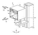
- a Y guide 21 which is a moving path extending in the Y direction, that is, a moving path extending linearly toward the back as viewed from the EFEM 101, is provided at the center in the X direction at the bottom of the processing block 102.
- the processing block 102 is provided with a support column 22 that forms a moving unit that is movable in the Y direction while being guided by the Y guide 21.
- the support unit 22 can be moved up and down along the support column 22 on the EFEM 101 side.
- a substrate mounting portion 3 is provided. The region in which the substrate platform 3 moves is set to an atmospheric pressure atmosphere such as an air atmosphere.
- a driving pulley and a driven pulley driven by a driving source are provided at positions corresponding to both ends of the Y guide 21, respectively.
- a belt conveyance mechanism or the like configured by hanging a belt and fixing the column portion 22 to the belt can be applied.
- each processing unit U is configured as the same structure, and is supported by a structure (not shown) including, for example, a column fixed to the floor surface.
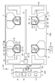
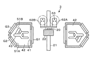
- the load lock module 4 has, for example, a load lock chamber in which one side extends along the Y guide 21 and a transfer port 41 for carrying in and out the wafer W is formed in a wall portion corresponding to the one side, and the planar shape is a pentagonal shape. 42 is provided. Therefore, the transport port 41 is arranged so as to face the moving area of the substrate mounting unit 3 described above. The transport port 41 is opened and closed by a gate valve G1.
- a substrate transport mechanism 43 including a joint arm that is rotatable around a vertical axis.
- the load lock chamber 42 is connected to an exhaust pipe for evacuation by an evacuation mechanism, and is configured so that the atmosphere can be switched between an atmospheric pressure atmosphere, for example, an air atmosphere and a vacuum atmosphere. Has been.
- the vacuum processing chamber of the first processing module 5A and the vacuum processing chamber of the second processing module 5B are respectively connected to the two sides on the back side when viewed from the transfer port 41 in the load lock chamber 42 via the transfer ports 51A and 51B. Airtight connection.
- the transport ports 51A and 51B are opened and closed by gate valves G2 and G3, respectively.
- the processing module and the vacuum processing chamber are denoted by the same reference numerals, and therefore the vacuum processing chamber is not labeled.
- the substrate transport mechanism 43 delivers the wafer W between the substrate platform 3, the first processing module 5A, and the second processing module 5B.
- Each of the first processing module 5A and the second processing module 5B is configured to be able to perform a film forming process which is, for example, a vacuum process, a wafer W mounting table, a processing gas supply unit for the film forming process, A cleaning gas supply unit for dry-cleaning the inside of the vacuum processing chamber, an exhaust port for evacuation by a vacuum evacuation mechanism, and the like are provided.
- a plasma generation mechanism is provided in the case of performing plasma processing. In FIG.
- a portion indicated by reference numeral 50 on the side of each processing unit U indicates a device arrangement region in which a gas supply device, a high-frequency power source for generating plasma, and the like are arranged. Since the structure of the film forming apparatus in a vacuum atmosphere is well known, the structure of the processing module is not particularly illustrated.
- the substrate platform 3 has left and right peripheral portions of the wafer W on both side surfaces inside the box 31 whose front surface opens as a substrate transfer port.
- a plurality of sets of holding portions 32 made up of ridges extending in the front-rear direction are provided in the vertical direction. That is, in the box 31, a plurality of wafers W are held in a shelf shape.
- the substrate platform 3 is provided via a rotating mechanism 24 on an elevator 23 that is an elevator that is provided so as to be movable up and down on a support column 22 that is a movable unit that can move in the Y direction.
- the rotation mechanism 24 includes a rotation shaft 25 that can rotate around a vertical axis and a rotation drive unit 26 that rotates the rotation shaft 25, and the bottom surface of the box 31 is fixed to the top of the rotation shaft 25. Therefore, the substrate platform 3 is configured to be freely movable in the Y direction, freely movable up and down, and rotatable about the vertical axis.
- the substrate mounting unit 3 plays a role of transferring the wafer W between the transfer mechanism 12 in the EFEM 101 and the substrate transfer mechanism 43 in the load lock module 4. For this reason, when the front surface of the substrate platform 3 faces the opening 17 on the back surface of the EFEM 101, the transfer mechanism 12 transfers the wafer W, and the front surface is connected to the transfer port 41 of the load lock chamber 42. When facing each other, the substrate transfer mechanism 43 transfers the wafer W.
- the rotation center of the substrate platform 3 may be positioned at the center of the substrate platform 3 in the front-rear direction and the left-right direction.
- the center of the substrate platform 3 is the center in the left-right direction.
- the center is displaced rearward from the center in the front-rear direction. Therefore, when the front surface of the substrate platform 3 is directed to the left, the substrate platform 3 is moved to the left as viewed from the center in the left-right direction, and when the front surface is directed to the right, the substrate platform 3 is moved to the right. Therefore, the advance / retreat stroke of the substrate transfer mechanism 43 in the load lock module 4 can be shortened.
- the wafer W received by the substrate platform 3 from the delivery mechanism 12 of the EFEM 101 is an unprocessed wafer W
- the wafer W received from the substrate transfer mechanism 43 in the load lock module 4 is a processed wafer W.
- the number of mounted wafers W depends on the operation mode in consideration of the time required for vacuum processing performed in the processing module 5A (5B), or whether any processing unit U is performing maintenance or the like. It depends on. For this reason, the number of stages (storage capacity) of the holding unit 32 in the substrate platform 3 is determined according to the maximum number of mounted sheets corresponding to the operation mode performed by the user.
- the number of stages of the holding unit 32 is received from the EFEM 101 side. It is necessary to set the number obtained by adding one to the number of mounted unprocessed wafers W. For example, when the substrate platform 3 receives 12 wafers W from the EFEM 101 side and distributes and transports them to each processing unit U, it is necessary to provide one substrate in the substrate platform 3, that is, A 13-stage holding portion 32 is required. When there are two substrate holding portions (pick) of the substrate transport mechanism 43, it is not necessary to provide a space for one holding portion 32.
- each processing unit U there is an operation mode in which cleaning is performed on one of the first processing module 5A and the second processing module 5B while the film processing is performed on the wafer W.
- Such an operation mode is applied when a long time is required for the film formation process.
- a process of forming a silicon oxide film using monosilane (SiH 4 ) gas and nitrogen dioxide (NO 2 ) gas and monosilane For example, the step of forming a silicon nitride film using SiH 4 ) gas and ammonia (NH 3 ) gas may be repeated many times.
- first processing module 5A and the second processing module 5B are performing the processing of the number of stacks that is half the target number of thin films on the wafer W, on the other side, Cleaning is performed, and then one of the remaining stacks is cleaned while the other half is processed.
- the number of unprocessed wafers W that the substrate platform 3 receives from the delivery mechanism 12 of the EFEM 101 is, for example, 12 sheets.
- the number of wafers W received by the substrate platform 3 from the EFEM 101 side Is, for example, six.
- the operation mode is not limited to such an example, and the film forming process is performed using both the first processing module 5A and the second processing module 5B of each processing unit U in parallel. May be.
- the number of wafers W received by the substrate platform 3 from the EFEM 101 side may be, for example, 24 corresponding to four groups of processing units U, or may be 12 of the half. . That is, the number of unprocessed wafers W received by the substrate platform 3 from the EFEM 101 side can be set to the number that provides the highest throughput according to the time required for the film forming process, the operation method, and the like.
- the substrate platform 3 used in the present embodiment has a structure superior to the transfer by the transfer arm and the known wafer shuttle.
- the substrate processing apparatus of the present embodiment includes a control unit 100 including a computer, and the control unit 100 includes a storage unit (not shown) that stores software necessary for operation.
- the software is linked to a process recipe in which a procedure and parameter values for executing processing performed on the wafer W are written, a program including steps included in the wafer W transfer sequence, and the process recipe.
- a program for determining an appropriate number of unprocessed wafers W carried into the substrate platform 3 is included.
- This software is stored in the storage unit via a storage medium such as an SSD (solid state drive), a hard disk, a compact disk, a magnetic optical disk, or a memory card.
- SSD solid state drive
- the opening / closing door 14 is opened, and the wafer W is taken out from the carrier C by the delivery mechanism 12.
- the substrate platform 3 is waiting at a position where the front surface faces the opening 17 on the back surface of the EFEM 101, and the wafer W held by the delivery mechanism 12 is delivered to the substrate platform 3 through the aperture 17.
- the height position of the wafer W is controlled by, for example, fixing the height position of the substrate platform 3 and adjusting the height of the transfer mechanism 12. This is done by controlling.
- the support unit 22 is viewed from the EFEM 101 on the front side of the processing unit U.
- the substrate platform 3 rises to a height position corresponding to the uppermost processing unit U. Then, the substrate platform 3 rotates, for example, to the left, and the front surface faces the transfer port 41 of the load lock chamber 42 of the processing unit U on the left side of the Y guide 21.
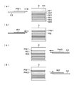
- the wafer W that has already been processed is transferred from, for example, the second processing module 5B into the load lock chamber 42 by the substrate transfer mechanism 43, and the inside of the load lock chamber 42 is always in the normal state. It is a pressure atmosphere. Subsequent wafer delivery will be described with reference to FIG. In FIG. 6, wafers W1 to W6 indicate unprocessed wafers.
- the gate valve G1 of the load lock chamber 42 is opened, and the processed wafer PW1 is first transferred by the substrate transfer mechanism 43 to the empty area R1 above the area where the wafer W is held in the substrate platform 3 (FIG. 6 (a)).
- the height position of the uppermost wafer W1 among the six unprocessed wafers W1 to W6 in the substrate platform 3 corresponds to the access position of the substrate transport mechanism 43.
- the substrate platform 3 is raised, and the uppermost wafer W1 is loaded into the load lock chamber 42 by the substrate transfer mechanism 43 (FIG. 6B).
- the empty area after the wafer W1 is extracted is indicated by R2.
- the substrate platform 3 rotates to the right side, for example, and the front surface faces the right side of the Y guide 21 and the transfer port 41 of the load lock chamber 42 of the uppermost processing unit U, and the load lock chamber of the processing unit U is concerned. 42 gate valve G1 is opened.
- the processed wafer PW2 is transferred to the above-described empty area R2 of the substrate platform 3 by the substrate transfer mechanism 43 (FIG. 6C).
- the substrate transport mechanism 43 is degenerated, the height position of the wafer W2 that is one stage below the wafer W1 already extracted in the substrate platform 3 corresponds to the access position of the substrate transport mechanism 43.
- the substrate platform 3 is raised, and the wafer W2 is loaded into the load lock chamber 42 by the substrate transfer mechanism 43 (FIG. 6D).
- the substrate platform 3 rotates to the left side, for example, and descends to a height position corresponding to the second stage processing unit U, and the processed wafer W in the processing unit U enters the substrate platform 3.
- the unprocessed wafer W3 in the substrate platform 3 is transferred into the processing unit U.
- the unprocessed wafers W1 to W6 of the substrate platform 3 are transferred to the left and right three-stage processing units U, and the processed wafers W are received from these processing units U.
- the front surface of the substrate platform 3 returns to the position facing the opening 17 on the back surface of the EFEM 101, and the processed wafers W in the substrate platform 3 are sequentially taken out through the aperture 17 by the delivery mechanism 12, for example, the original Returned to carrier C.
- the wafer W carried into the load lock chamber 42 is first transferred to the first processing module 5A, and, for example, alternating deposition of a silicon oxide film and a silicon nitride film is performed a predetermined number of times. For example, when both films are counted as one layer, the number of stacked layers is half of the target number of layers, and the cleaning process is performed in the second processing module 5B during that time.
- the cleaning process is performed using, for example, nitrogen trifluoride (NF 3 ) gas in order to remove the thin films (silicon oxide film and silicon nitride film) adhering to the inside of the vacuum processing container.
- NF 3 nitrogen trifluoride
- the wafer W is transferred to the second processing module 5B, and the remaining number of stacked films is formed. Processing is performed.
- the wafer W is carried into the load lock chamber 42 and transferred to the substrate platform 3 as described above, and the next unprocessed wafer W is the first unprocessed wafer W.
- the film forming process is performed in the same manner.
- the unprocessed wafers W are similarly transferred to the left and right processing units U.
- the film formation start time in the front left and right processing units U and the film formation start time in the back left and right processing units U are shifted by a predetermined time.
- the substrate platform 3 delivers the processed wafer W received from the left and right processing units U on the front side to the EFEM 101, and then receives the unprocessed wafer W to be processed in the left and right processing units U from the EFEM 101. Then, the processed wafer W and the unprocessed wafer W are exchanged between the placement unit 3 and the left and right processing units U.
- the deviation of the start time described above is set so that the processed wafer W does not wait unnecessarily in both the front processing unit U and the back processing unit U in such a series of operations. Note that a sequence including the position control of the series of substrate placement units 3 is executed by a program in the control unit 100 constituting the transfer sequence.
- a group in which the processing units U including the two processing modules 5A and 5B and the load lock module 4 are arranged in three stages is moved back and forth along the Y guide 21 extending toward the back as viewed from the EFEM 101.
- four groups are provided on the left and right sides of the Y guide 21. Then, in one movement of the substrate platform 3 between the EFEM 101 and the processing unit U, unprocessed wafers W corresponding to the number of processed wafers W are mounted on the substrate platform 3 and distributed and conveyed. The processed wafer W is received by the substrate platform 3 and transferred to the EFEM 101. Therefore, a high throughput can be obtained (a large number of processed sheets per unit time), and a substrate processing apparatus having a large processing capability can be constructed.
- the substrate platform 3 is configured such that a plurality of wafers W can be placed in a shelf shape, and the wafer W can be delivered by the delivery mechanism 12 of the EFEM 101 and the substrate transport mechanism 42 of the processing unit U.
- the structure is not limited to the above-described embodiment. 7 and 8 show the substrate platform 3 used in the second embodiment of the substrate processing apparatus of the present invention.
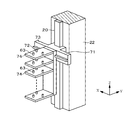
- the substrate platform 3 is provided with a plate-like lifting base 61 that moves up and down while being guided by a Z guide 20 provided on the front side of the support column 22.
- the elevating base 61 has a vertically long portion on the left and right and is formed in a shape in which these vertically long portions are connected to each other with a horizontally long portion.
- four stages of mounting tables 62A and 62B are provided on each of the left and right vertical portions of the elevating base 61 so as to protrude horizontally toward the front side, that is, toward the EFEM 101 side.
- Three holding pins 63 that are protrusions for holding the wafer W are provided on the upper surfaces of the mounting tables 62A and 62B. With respect to the three holding pins 63, the substrate holding portions (picks) of the delivery mechanism 12 and the substrate transport mechanism 43 can enter between the upper surfaces of the mounting tables 62 ⁇ / b> A and 62 ⁇ / b> B and the wafer W, and the holding pins 63.
- the height and arrangement layout are set so as not to interfere with each other in a plane.
- the left four-stage mounting table 62A is for transferring the substrate to and from the substrate transport mechanism 43 of the left processing module 4
- the right four-stage mounting table 62B is the right processing module 4
- the substrate is transferred to and from the substrate transport mechanism 43.
- the configuration other than the substrate placement unit 3 is the same as that of the first embodiment.
- the unprocessed wafer W is transferred to the mounting tables 62A and 62B of the substrate mounting unit 3 by performing the horizontal movement of the transfer mechanism 12 in addition to the lifting and lowering operation of the transfer mechanism 12 of the EFEM 101.
- the uppermost mounting tables 62A and 62B are not provided with the wafer W and are vacant spaces.
- the substrate platform 3 is sequentially rotated to the left and right, and the wafer W is transferred between the left processing unit U and the right processing unit U.
- the wafer W is transferred to and from the processing unit U without rotating the substrate platform 3. That is, the processed wafer W is transferred from the load lock chamber 42 to the uppermost stage mounting table 62A on the left side of the substrate platform 3 by the substrate transfer mechanism 43 in the loadlock chamber 42 of the uppermost processing unit U on the left side.
- the unprocessed wafer W on the second stage mounting table 62 A is carried into the load lock chamber 42 by the substrate transfer mechanism 43.
- the same wafer W is also transferred between the substrate transfer mechanism 43 in the load lock chamber 42 of the uppermost processing unit U on the right side and the mounting table 62A on the right side of the substrate mounting unit 3.
- the left and right substrate transfer mechanisms 43 simultaneously transfer the wafer W to the left and right mounting tables 62A and 62B.
- the elevating base 61 is lowered to a position corresponding to the second stage processing unit U.
- the left and right mounting tables are respectively formed by the substrate transfer mechanism 43 in the load lock chamber 42 of the left second stage processing unit U and the substrate transfer mechanism 43 in the load lock chamber 42 of the right second stage processing unit U.
- the wafer W is simultaneously transferred to the 62A and 62B in the same manner.
- the same delivery is performed between the processing unit U at the third stage and the substrate platform 3, and the substrate platform 3 has the processed wafers W mounted on the left and right platforms 62A and 62B, respectively.
- the position returns to the position facing the opening 17 on the back surface of the EFEM 101.
- Each of the left and right mounting tables 62A and 62B is arranged in four stages, but this configuration is merely an example.
- the arrangement is a seven-stage arrangement, and the left mounting table 62A has processing units U arranged on the left and right sides. Six unprocessed wafers W are mounted for transfer to each of the wafers, and six unprocessed wafers W for transfer to each of the processing units U disposed at the front and rear of the right side on the right mounting table 62B. It may be an operation to install.
- the substrate mounting section 3 is provided with a plurality of stages of mounting tables 62A and 62B on the left and right sides, a load lock can be achieved without using a rotating mechanism as in the first embodiment. There is an advantage that the substrate transfer mechanism 43 in the chamber 42 can deliver the wafer W with a short stroke.
- FIG. 9 shows the substrate platform 3 used in the third embodiment of the substrate processing apparatus of the present invention.
- the substrate platform 3 is provided with a horizontally elevating base 71 that moves up and down while being guided by a Z guide 20 provided on the front side of the support column 22.
- the elevating base 71 is provided with an X guide 72 extending in the X direction, and a vertically long X moving body 73 that is guided by the X guide 72 and can move in the X direction.
- Examples of the moving mechanism for moving the X moving body 73 include a belt conveyance mechanism and a ball screw mechanism.
- the X moving body 73 is provided with, for example, seven stages of mounting tables 74 having the same structure as the mounting tables 62A (62B) used in the second embodiment.
- the top stage mounting table 74 among the seven stages mounting table 74 is set as an empty space, and a total of six unprocessed wafers W are mounted on the second and subsequent mounting tables 74 by the delivery mechanism 12. Then, the support column 21 is moved to a position corresponding to the processing unit U on the near side, and the substrate mounting unit 3 is raised to a position corresponding to the uppermost processing unit U by the elevating base 71.
- the X moving body 72 is positioned at the left side, and the processed wafer W is delivered to the uppermost mounting table 74 by the substrate transfer mechanism 43 of the load lock chamber 42 as already described in detail.
- the unprocessed wafer W on the mounting table 74 is transferred to the substrate transfer mechanism 43.
- the elevating base 71 is raised by one stage of the mounting table 74 and the X moving body 72 is positioned at the right side, and the processed wafer W is placed on the second stage mounting table from the uppermost processing unit U side on the right side. Pass to 74.
- the X moving body 72 is sequentially moved to the left and right, and the height position of the elevating base 71 is set to a position corresponding to each processing unit U, whereby the substrate mounting portion 3 and the left and right processing units U on the near side are set.
- the processed wafer W and the unprocessed wafer W are delivered (exchanged). That is, in this example, the position where the X moving body 72 is moved to the left side and the position which is moved to the right side correspond to the positions of the mounting tables 62A and 62B of the second embodiment, respectively.
- the stroke of the substrate transport mechanism 43 may be short, but a vertically long member constituting the X moving body 72 may be fixed at an intermediate position between the left and right processing units U. Even this configuration can be applied if the stroke of the substrate transport mechanism 43 can be accommodated.
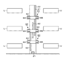
- FIG. 10 and FIG. 11 show the substrate platform 3 used in the fourth embodiment of the substrate processing apparatus of the present invention.
- the substrate mounting unit 3 includes a first mounting table unit 81 for transferring a substrate to and from the uppermost processing unit U among the three processing units U, a second processing unit U, A second mounting table unit 82 for transferring a substrate between them, and a third mounting table unit 83 for transferring a substrate between the third-stage processing unit U. .
- the first to third mounting table units 81 to 83 can transfer the wafer W to the first to third stage processing units U, and can transfer the wafer W to and from the transfer mechanism 12 of the EFEM 101.
- the upper and lower movement ranges are assigned, and they can be moved up and down independently of each other.
- first to third Z guides 91 to 91 which are guide paths for guiding the first to third mounting table units 81 to 83 to move up and down, respectively, are provided on the support column 22. 93 is provided.
- Each of the first to third mounting table units 81 to 83 includes, for example, a horizontally long elevating base 84, and the elevating base 84 is raised and lowered while being guided by first to third Z guides 91 to 93.
- a belt conveying mechanism, a ball screw mechanism, or the like is used as a mechanism for raising and lowering the first to third mounting table units 81 to 83.
- Each lifting base 84 is provided with a two-stage mounting table 8A on the left side and a two-stage mounting table 8B on the right side.
- the horizontal position of the left two-stage mounting table 8A and the horizontal position of the right two-stage mounting table 8A are respectively the positions of the left mounting table 62A and the right mounting table 62B in the second embodiment. It corresponds. That is, the left two-stage mounting table 8A transfers wafers W to and from the left processing unit U, and the right two-stage mounting table 8B transfers wafers to and from the right processing unit U. W is handed over.
- the set of the two stage mounting tables 8A on the left side of the first to third mounting table units 81 to 83 has a wafer W between each of the upper, middle and lower processing units U in the left processing unit U. Will be delivered.
- the set of the two stage mounting bases 8B on the right side of the first to third mounting base units 81 to 83 is arranged between the upper, middle and lower processing units U in the right processing unit U. Delivery will be performed.
- One and the other of the upper stage side and the lower stage side of the two stage mounting tables 8A or 8B forming the set are for mounting the unprocessed wafer W and the processed wafer W, respectively.
- the lower stage of the two stages of the left mounting table 8A in the first to third mounting table units 81 to 83 for example, the lower stage of the two stages of the right mounting table 8B
- the unprocessed wafer W is transferred by the transfer mechanism 12.
- the first to third mounting table units 81 to 83 are set to height positions corresponding to the upper, middle, and lower processing units U, respectively, in the processing unit U on the front side, for example, The processed wafers W are simultaneously transferred between the middle and lower processing units U and the upper, middle and lower processing units U on the right side, and the unprocessed wafers W are simultaneously transferred.
- the fourth embodiment is an effective technique in terms of improving the throughput.
- the first to third mounting table units 81 to 83 are not limited to the two-stage set of mounting tables 8A (8B) provided on the left and right, but are processing units facing the left and right. You may make it provide the 2 step
- the substrate platform 3 first to third platform units 81 to 83
- the processing units U are arranged in three stages on the left and right, but may be arranged in two stages or four or more stages. Further, the processing units U are not limited to being arranged in two groups on the front and rear along the Y guide 21, but may be arranged in three groups or only one group. Furthermore, the processing unit U may be disposed only on one side of the Y guide 21.
- the vacuum processing in the processing modules 5A and 5B is not limited to the film forming process, and may be an annealing process, an etching process, or the like.
- the first and second processing modules 5A and 5B may be applied to the wafer W in parallel. The same vacuum treatment may be performed on the same. Alternatively, the first and second processing modules 5A and 5B may be operated in such a manner that different processes are continuously performed.
- each processing unit may be provided with one or three or more processing modules.
- the processing performed in the processing module is not limited to the vacuum processing, and may be, for example, a wet cleaning process in which the wafer W is adsorbed onto the spin chuck and the cleaning liquid is supplied in the air atmosphere. No module is needed.
- the substrate is not limited to a wafer but may be a glass substrate used for a liquid crystal panel or the like.
Priority Applications (3)
| Application Number | Priority Date | Filing Date | Title |
|---|---|---|---|
| KR1020197001350A KR102164404B1 (ko) | 2016-07-22 | 2017-06-21 | 기판 처리 장치 |
| CN201780044348.2A CN109478527B (zh) | 2016-07-22 | 2017-06-21 | 基片处理设备 |
| US16/252,978 US10906756B2 (en) | 2016-07-22 | 2019-01-21 | Substrate processing device |
Applications Claiming Priority (2)
| Application Number | Priority Date | Filing Date | Title |
|---|---|---|---|
| JP2016144764A JP6747136B2 (ja) | 2016-07-22 | 2016-07-22 | 基板処理装置 |
| JP2016-144764 | 2016-07-22 |
Related Child Applications (1)
| Application Number | Title | Priority Date | Filing Date |
|---|---|---|---|
| US16/252,978 Continuation US10906756B2 (en) | 2016-07-22 | 2019-01-21 | Substrate processing device |
Publications (1)
| Publication Number | Publication Date |
|---|---|
| WO2018016257A1 true WO2018016257A1 (ja) | 2018-01-25 |
Family
ID=60992105
Family Applications (1)
| Application Number | Title | Priority Date | Filing Date |
|---|---|---|---|
| PCT/JP2017/022866 WO2018016257A1 (ja) | 2016-07-22 | 2017-06-21 | 基板処理装置 |
Country Status (5)
| Country | Link |
|---|---|
| US (1) | US10906756B2 (zh) |
| JP (1) | JP6747136B2 (zh) |
| KR (1) | KR102164404B1 (zh) |
| CN (1) | CN109478527B (zh) |
| WO (1) | WO2018016257A1 (zh) |
Cited By (2)
| Publication number | Priority date | Publication date | Assignee | Title |
|---|---|---|---|---|
| CN112689891A (zh) * | 2018-09-21 | 2021-04-20 | 东京毅力科创株式会社 | 真空处理装置和基板输送方法 |
| TWI835914B (zh) | 2018-11-14 | 2024-03-21 | 日商東京威力科創股份有限公司 | 基板處理裝置及基板搬送方法 |
Families Citing this family (4)
| Publication number | Priority date | Publication date | Assignee | Title |
|---|---|---|---|---|
| JP6851288B2 (ja) * | 2017-08-23 | 2021-03-31 | 東京エレクトロン株式会社 | 基板処理装置及び基板搬送方法 |
| US11380564B2 (en) * | 2018-09-19 | 2022-07-05 | Applied Materials, Inc. | Processing system having a front opening unified pod (FOUP) load lock |
| JP7214834B2 (ja) * | 2019-03-19 | 2023-01-30 | 株式会社Kokusai Electric | 半導体装置の製造方法、基板処理装置およびプログラム |
| US11705354B2 (en) * | 2020-07-10 | 2023-07-18 | Applied Materials, Inc. | Substrate handling systems |
Citations (5)
| Publication number | Priority date | Publication date | Assignee | Title |
|---|---|---|---|---|
| WO2001075965A1 (fr) * | 2000-04-05 | 2001-10-11 | Tokyo Electron Limited | Dispositif de traitement |
| JP2002334918A (ja) * | 2001-03-09 | 2002-11-22 | Tokyo Electron Ltd | 処理装置 |
| JP2003197709A (ja) * | 2001-12-25 | 2003-07-11 | Tokyo Electron Ltd | 被処理体の搬送機構及び処理システム |
| JP2008028035A (ja) * | 2006-07-19 | 2008-02-07 | Phyzchemix Corp | 半導体製造装置 |
| JP2014068009A (ja) * | 2012-09-12 | 2014-04-17 | Lam Research Corporation | 半導体処理装置に関する方法およびシステム |
Family Cites Families (9)
| Publication number | Priority date | Publication date | Assignee | Title |
|---|---|---|---|---|
| KR0147403B1 (ko) * | 1994-06-24 | 1998-11-02 | 문정환 | 칩자동 로딩장치 |
| JP2003188229A (ja) | 2001-12-18 | 2003-07-04 | Hitachi Kasado Eng Co Ltd | ウエハ製造システムおよびウエハ製造方法 |
| JP2004349503A (ja) | 2003-05-22 | 2004-12-09 | Tokyo Electron Ltd | 被処理体の処理システム及び処理方法 |
| WO2005123565A2 (en) * | 2004-06-09 | 2005-12-29 | Brooks Automation, Inc. | Dual sacra arm |
| US7950407B2 (en) * | 2007-02-07 | 2011-05-31 | Applied Materials, Inc. | Apparatus for rapid filling of a processing volume |
| CN101330032B (zh) * | 2008-07-22 | 2012-01-11 | 北京北方微电子基地设备工艺研究中心有限责任公司 | 等离子体处理设备及其过渡腔室 |
| JP2011071293A (ja) * | 2009-09-25 | 2011-04-07 | Tokyo Electron Ltd | プロセスモジュール、基板処理装置、および基板搬送方法 |
| KR102060544B1 (ko) * | 2010-11-10 | 2019-12-30 | 브룩스 오토메이션 인코퍼레이티드 | 이중 아암 로봇 |
| TWI691388B (zh) * | 2011-03-11 | 2020-04-21 | 美商布魯克斯自動機械公司 | 基板處理裝置 |
-
2016
- 2016-07-22 JP JP2016144764A patent/JP6747136B2/ja active Active
-
2017
- 2017-06-21 KR KR1020197001350A patent/KR102164404B1/ko active IP Right Grant
- 2017-06-21 WO PCT/JP2017/022866 patent/WO2018016257A1/ja active Application Filing
- 2017-06-21 CN CN201780044348.2A patent/CN109478527B/zh active Active
-
2019
- 2019-01-21 US US16/252,978 patent/US10906756B2/en active Active
Patent Citations (5)
| Publication number | Priority date | Publication date | Assignee | Title |
|---|---|---|---|---|
| WO2001075965A1 (fr) * | 2000-04-05 | 2001-10-11 | Tokyo Electron Limited | Dispositif de traitement |
| JP2002334918A (ja) * | 2001-03-09 | 2002-11-22 | Tokyo Electron Ltd | 処理装置 |
| JP2003197709A (ja) * | 2001-12-25 | 2003-07-11 | Tokyo Electron Ltd | 被処理体の搬送機構及び処理システム |
| JP2008028035A (ja) * | 2006-07-19 | 2008-02-07 | Phyzchemix Corp | 半導体製造装置 |
| JP2014068009A (ja) * | 2012-09-12 | 2014-04-17 | Lam Research Corporation | 半導体処理装置に関する方法およびシステム |
Cited By (2)
| Publication number | Priority date | Publication date | Assignee | Title |
|---|---|---|---|---|
| CN112689891A (zh) * | 2018-09-21 | 2021-04-20 | 东京毅力科创株式会社 | 真空处理装置和基板输送方法 |
| TWI835914B (zh) | 2018-11-14 | 2024-03-21 | 日商東京威力科創股份有限公司 | 基板處理裝置及基板搬送方法 |
Also Published As
| Publication number | Publication date |
|---|---|
| US10906756B2 (en) | 2021-02-02 |
| CN109478527B (zh) | 2023-03-28 |
| US20190152722A1 (en) | 2019-05-23 |
| KR20190020042A (ko) | 2019-02-27 |
| JP6747136B2 (ja) | 2020-08-26 |
| CN109478527A (zh) | 2019-03-15 |
| KR102164404B1 (ko) | 2020-10-12 |
| JP2018014469A (ja) | 2018-01-25 |
Similar Documents
| Publication | Publication Date | Title |
|---|---|---|
| WO2018016257A1 (ja) | 基板処理装置 | |
| JP6006643B2 (ja) | 真空処理装置 | |
| JP5883232B2 (ja) | 基板処理装置 | |
| JP5503006B2 (ja) | 基板処理システム、搬送モジュール、基板処理方法及び半導体素子の製造方法 | |
| JP4980978B2 (ja) | 基板処理装置 | |
| JP2010192855A (ja) | 基板処理装置 | |
| JP2011071293A (ja) | プロセスモジュール、基板処理装置、および基板搬送方法 | |
| US10872798B2 (en) | Substrate transfer mechanism, substrate processing apparatus, and substrate transfer method | |
| TW201342518A (zh) | 真空處理裝置及真空處理裝置之運轉方法 | |
| US20110135427A1 (en) | Method for transferring target object and apparatus for processing target object | |
| TW202147503A (zh) | 半導體處理系統 | |
| US9199805B2 (en) | Processing system and processing method | |
| US20090162170A1 (en) | Tandem type semiconductor-processing apparatus | |
| KR101336420B1 (ko) | 진공 처리 장치 | |
| KR101383248B1 (ko) | 고속 기판 처리 시스템 | |
| JP2014060338A (ja) | 基板処理装置 | |
| KR101578081B1 (ko) | 기판처리시스템 | |
| JP2021145017A (ja) | 基板搬送システム、真空基板搬送モジュール、および基板搬送方法 | |
| JP2004080053A (ja) | 半導体製造装置 | |
| TW202341320A (zh) | 用於混合式基板接合系統的foup或卡匣儲存器 | |
| KR101649303B1 (ko) | 기판처리시스템 | |
| KR20230111438A (ko) | 반도체 기판 처리 장치 | |
| JP2013055363A (ja) | プロセスモジュール、基板処理装置、および基板搬送方法 | |
| JP2001358192A (ja) | 半導体製造設備 | |
| JP2012186506A (ja) | マルチ−チャンバーシステムで半導体素子を製造する方法 |
Legal Events
| Date | Code | Title | Description |
|---|---|---|---|
| 121 | Ep: the epo has been informed by wipo that ep was designated in this application |
Ref document number: 17830777 Country of ref document: EP Kind code of ref document: A1 |
|
| ENP | Entry into the national phase |
Ref document number: 20197001350 Country of ref document: KR Kind code of ref document: A |
|
| NENP | Non-entry into the national phase |
Ref country code: DE |
|
| 122 | Ep: pct application non-entry in european phase |
Ref document number: 17830777 Country of ref document: EP Kind code of ref document: A1 |