WO2018012019A1 - シリコンウェーハの評価方法及び製造方法 - Google Patents
シリコンウェーハの評価方法及び製造方法 Download PDFInfo
- Publication number
- WO2018012019A1 WO2018012019A1 PCT/JP2017/006727 JP2017006727W WO2018012019A1 WO 2018012019 A1 WO2018012019 A1 WO 2018012019A1 JP 2017006727 W JP2017006727 W JP 2017006727W WO 2018012019 A1 WO2018012019 A1 WO 2018012019A1
- Authority
- WO
- WIPO (PCT)
- Prior art keywords
- silicon wafer
- thermal donor
- single crystal
- defect
- region
- Prior art date
- Legal status (The legal status is an assumption and is not a legal conclusion. Google has not performed a legal analysis and makes no representation as to the accuracy of the status listed.)
- Ceased
Links
Images




Classifications
-
- C—CHEMISTRY; METALLURGY
- C30—CRYSTAL GROWTH
- C30B—SINGLE-CRYSTAL GROWTH; UNIDIRECTIONAL SOLIDIFICATION OF EUTECTIC MATERIAL OR UNIDIRECTIONAL DEMIXING OF EUTECTOID MATERIAL; REFINING BY ZONE-MELTING OF MATERIAL; PRODUCTION OF A HOMOGENEOUS POLYCRYSTALLINE MATERIAL WITH DEFINED STRUCTURE; SINGLE CRYSTALS OR HOMOGENEOUS POLYCRYSTALLINE MATERIAL WITH DEFINED STRUCTURE; AFTER-TREATMENT OF SINGLE CRYSTALS OR A HOMOGENEOUS POLYCRYSTALLINE MATERIAL WITH DEFINED STRUCTURE; APPARATUS THEREFOR
- C30B15/00—Single-crystal growth by pulling from a melt, e.g. Czochralski method
- C30B15/20—Controlling or regulating
-
- C—CHEMISTRY; METALLURGY
- C30—CRYSTAL GROWTH
- C30B—SINGLE-CRYSTAL GROWTH; UNIDIRECTIONAL SOLIDIFICATION OF EUTECTIC MATERIAL OR UNIDIRECTIONAL DEMIXING OF EUTECTOID MATERIAL; REFINING BY ZONE-MELTING OF MATERIAL; PRODUCTION OF A HOMOGENEOUS POLYCRYSTALLINE MATERIAL WITH DEFINED STRUCTURE; SINGLE CRYSTALS OR HOMOGENEOUS POLYCRYSTALLINE MATERIAL WITH DEFINED STRUCTURE; AFTER-TREATMENT OF SINGLE CRYSTALS OR A HOMOGENEOUS POLYCRYSTALLINE MATERIAL WITH DEFINED STRUCTURE; APPARATUS THEREFOR
- C30B15/00—Single-crystal growth by pulling from a melt, e.g. Czochralski method
- C30B15/20—Controlling or regulating
- C30B15/203—Controlling or regulating the relationship of pull rate (v) to axial thermal gradient (G)
-
- C—CHEMISTRY; METALLURGY
- C30—CRYSTAL GROWTH
- C30B—SINGLE-CRYSTAL GROWTH; UNIDIRECTIONAL SOLIDIFICATION OF EUTECTIC MATERIAL OR UNIDIRECTIONAL DEMIXING OF EUTECTOID MATERIAL; REFINING BY ZONE-MELTING OF MATERIAL; PRODUCTION OF A HOMOGENEOUS POLYCRYSTALLINE MATERIAL WITH DEFINED STRUCTURE; SINGLE CRYSTALS OR HOMOGENEOUS POLYCRYSTALLINE MATERIAL WITH DEFINED STRUCTURE; AFTER-TREATMENT OF SINGLE CRYSTALS OR A HOMOGENEOUS POLYCRYSTALLINE MATERIAL WITH DEFINED STRUCTURE; APPARATUS THEREFOR
- C30B29/00—Single crystals or homogeneous polycrystalline material with defined structure characterised by the material or by their shape
- C30B29/02—Elements
- C30B29/06—Silicon
-
- C—CHEMISTRY; METALLURGY
- C30—CRYSTAL GROWTH
- C30B—SINGLE-CRYSTAL GROWTH; UNIDIRECTIONAL SOLIDIFICATION OF EUTECTIC MATERIAL OR UNIDIRECTIONAL DEMIXING OF EUTECTOID MATERIAL; REFINING BY ZONE-MELTING OF MATERIAL; PRODUCTION OF A HOMOGENEOUS POLYCRYSTALLINE MATERIAL WITH DEFINED STRUCTURE; SINGLE CRYSTALS OR HOMOGENEOUS POLYCRYSTALLINE MATERIAL WITH DEFINED STRUCTURE; AFTER-TREATMENT OF SINGLE CRYSTALS OR A HOMOGENEOUS POLYCRYSTALLINE MATERIAL WITH DEFINED STRUCTURE; APPARATUS THEREFOR
- C30B33/00—After-treatment of single crystals or homogeneous polycrystalline material with defined structure
- C30B33/02—Heat treatment
-
- H—ELECTRICITY
- H10—SEMICONDUCTOR DEVICES; ELECTRIC SOLID-STATE DEVICES NOT OTHERWISE PROVIDED FOR
- H10P—GENERIC PROCESSES OR APPARATUS FOR THE MANUFACTURE OR TREATMENT OF DEVICES COVERED BY CLASS H10
- H10P36/00—Gettering within semiconductor bodies
- H10P36/20—Intrinsic gettering, i.e. thermally inducing defects by using oxygen present in the silicon body
-
- H—ELECTRICITY
- H10—SEMICONDUCTOR DEVICES; ELECTRIC SOLID-STATE DEVICES NOT OTHERWISE PROVIDED FOR
- H10P—GENERIC PROCESSES OR APPARATUS FOR THE MANUFACTURE OR TREATMENT OF DEVICES COVERED BY CLASS H10
- H10P74/00—Testing or measuring during manufacture or treatment of wafers, substrates or devices
- H10P74/20—Testing or measuring during manufacture or treatment of wafers, substrates or devices characterised by the properties tested or measured, e.g. structural or electrical properties
- H10P74/203—Structural properties, e.g. testing or measuring thicknesses, line widths, warpage, bond strengths or physical defects
-
- H—ELECTRICITY
- H10—SEMICONDUCTOR DEVICES; ELECTRIC SOLID-STATE DEVICES NOT OTHERWISE PROVIDED FOR
- H10P—GENERIC PROCESSES OR APPARATUS FOR THE MANUFACTURE OR TREATMENT OF DEVICES COVERED BY CLASS H10
- H10P90/00—Preparation of wafers not covered by a single main group of this subclass, e.g. wafer reinforcement
-
- H—ELECTRICITY
- H10—SEMICONDUCTOR DEVICES; ELECTRIC SOLID-STATE DEVICES NOT OTHERWISE PROVIDED FOR
- H10P—GENERIC PROCESSES OR APPARATUS FOR THE MANUFACTURE OR TREATMENT OF DEVICES COVERED BY CLASS H10
- H10P95/00—Generic processes or apparatus for manufacture or treatments not covered by the other groups of this subclass
-
- H—ELECTRICITY
- H10—SEMICONDUCTOR DEVICES; ELECTRIC SOLID-STATE DEVICES NOT OTHERWISE PROVIDED FOR
- H10P—GENERIC PROCESSES OR APPARATUS FOR THE MANUFACTURE OR TREATMENT OF DEVICES COVERED BY CLASS H10
- H10P95/00—Generic processes or apparatus for manufacture or treatments not covered by the other groups of this subclass
- H10P95/90—Thermal treatments, e.g. annealing or sintering
Definitions
- the present invention relates to a silicon wafer evaluation method and manufacturing method, and more particularly to a crystal defect region evaluation method of a silicon wafer manufactured by the Czochralski method (hereinafter referred to as “CZ method”).
- CZ method a crystal defect region evaluation method of a silicon wafer manufactured by the Czochralski method
- the CZ method is a method of growing a single crystal by melting a polycrystalline raw material filled in a quartz crucible with a heater and then immersing a seed crystal in the melt and pulling it upward while rotating it.
- the FZ method is a method in which a part of a polycrystalline raw material rod is heated and melted at a high frequency to form a melting zone, and a single crystal is grown while moving the melting zone. Since the CZ method makes it easy to form a crystal with a large diameter, a wafer cut from a silicon single crystal manufactured by the CZ method is used as a highly integrated semiconductor element substrate.
- Silicon wafers manufactured by the CZ method are exposed to thermal oxidation treatment for 1 to 10 hours in an acidic atmosphere of 1000 to 1200 ° C., and appear to have an oxidation-induced stacking fault (hereinafter referred to as OSF (Oxidation-induced Stacking-Fault)) Ring)) may occur.
- OSF Oxidation-induced Stacking-Fault
- Ring oxidation-induced stacking fault
- several types of minute defects hereinafter referred to as “Grown-in defects”.
- the generation site of the OSF ring in the crystal includes a growth rate (pulling rate) V of the silicon single crystal and a temperature gradient G in the pulling axis direction in the temperature range from the melting point of the grown silicon single crystal to 1300 ° C.
- the ratio V / G When the V / G is larger than the critical value at which the OSF ring disappears at the center of the crystal, the vacancies agglomerate to form an octahedral void defect of about 0.1 ⁇ m, and a MOS type LSI is manufactured. In this case, the breakdown voltage of the gate oxide film is deteriorated, or an isolation defect in the element isolation region is caused. In addition, when trench capacitor is used, characteristic defects such as punch-through between the capacitor are caused. On the other hand, when V / G is smaller than the critical value, interstitial silicon aggregates to form dislocation clusters, leading to characteristic defects such as PN junction leakage.
- Patent Document 1 a ratio V / G between a pulling rate V and a temperature gradient G in a crystal is controlled in a single crystal growth so that no grown-in defect or OSF ring occurs (hereinafter referred to as a defect-free region). ) Has been proposed.
- a method for evaluating a Grown-in defect or an OSF ring for example, a method of detecting a void defect by infrared scattering tomography or an OSF ring that is manifested by etching after the thermal oxidation treatment at 1000 to 1200 ° C. described above with a microscope is used. The observation method is known.
- Patent Documents 2 and 3 describe a method for analyzing and evaluating crystal defects of a silicon wafer by a so-called copper decoration method.
- the analysis method described in Patent Document 2 includes a step of forming a thermal oxide film having a predetermined thickness on the surface of a bare wafer, a step of etching a bag side of the bare wafer, and copper at a defective portion of the bare wafer. And a step of analyzing a defect portion of the wafer decorated with copper after the step of performing copper decorating.
- the distribution and density of defect sites on the copper-decorated wafer are analyzed with the naked eye, and the morphology of the defect sites on the copper-decorated wafer is analyzed by transmission electron microscope (TEM) or scanning electron microscope (SEM). ) To analyze.
- TEM transmission electron microscope
- SEM scanning electron microscope
- Patent Document 3 describes a method of evaluating crystal defects in a silicon single crystal manufactured by the CZ method by a copper decoration method in which a sample contaminated with copper is heat-treated and then rapidly cooled.
- a copper decoration method is applied to a silicon single crystal having a low oxygen concentration with an interstitial oxygen concentration of 10 ⁇ 10 17 atoms / cm 3 (ASTM'79) or less in the crystal, and a nucleus that becomes OSF or OSF. The area where the is present is detected with high sensitivity.
- the film thickness of an epitaxial layer or a DZ layer in an epitaxial wafer is measured by measuring the resistivity of the wafer by a thermal donor generated from interstitial oxygen when the silicon wafer is annealed at a low temperature of about 450 ° C.
- a method for evaluating a wafer structure related to oxygen concentration distribution such as measurement is described.
- JP-A-8-330316 Japanese Patent Laid-Open No. 10-227729 JP 2001-81000 A JP-A-9-82768
- the conventional method for evaluating crystal defects of a general silicon wafer requires a plurality of heat treatments and etching processes according to the types of crystal defects, and there is a problem that the evaluation takes time and cost.
- the silicon wafer crystal defect evaluation method using the copper decoration method can simultaneously evaluate the presence or absence of a grown-in defect region or an OSF ring region, but a heat treatment process of several tens of hours for copper decoration. Is necessary, and there is a problem of lack of simplicity.
- an object of the present invention is to provide a silicon wafer evaluation method and manufacturing method capable of evaluating the presence and type of a crystal defect region of a silicon wafer by a simple method while saving time and cost.
- a silicon wafer evaluation method is an evaluation method of a silicon wafer cut out from a silicon single crystal ingot grown by a CZ method, and a thermal donor generation heat treatment is performed on the silicon wafer. It is characterized in that the generation rate of a thermal donor that is sometimes generated is measured, and the presence or absence of a crystal defect region or the type of crystal defect is determined based on the generation rate of the thermal donor.
- a thermal donor generation rate based on a change in specific resistance caused by heat treatment of a silicon wafer cut from a silicon single crystal ingot grown by the CZ method while controlling V / G is measured.
- the presence / absence of a crystal defect region and the type of crystal defect can be easily evaluated.
- the first silicon wafer cut out from the silicon single crystal ingot is subjected to the thermal donor generation heat treatment in a state where the first silicon wafer includes an oxygen cluster.
- the first thermal donor generation rate which is the generation rate of the thermal donor generated at the measurement point, was obtained, and the donor killer process and the thermal donor generation heat treatment were sequentially performed on the second silicon wafer different from the first silicon wafer.
- a second thermal donor generation rate that is a generation rate of a thermal donor generated at a second measurement point on the second silicon wafer is sometimes obtained, and a first thermal donor generation relative to the second thermal donor generation rate is obtained.
- the state in which the silicon wafer includes oxygen clusters refers to a state before the donor killer process is performed on the silicon wafer in the as-grown state.
- the defect-free region refers to a region that does not include a grown-in defect and does not generate an OSF ring after the evaluation heat treatment.
- the present invention based on the first and second thermal donor generation rates obtained from the two types of wafers having the difference in the presence or absence of the donor killer process, the presence or absence of the crystal defect region and the crystal defect The type can be easily evaluated.
- the silicon wafer evaluation method determines that the first measurement point on the first silicon wafer is a defect-free region when the thermal donor generation speed ratio is within the first speed range.
- the thermal donor generation speed ratio is in a second speed range higher than the first speed range, it is determined that the first measurement point is a region including a void defect, and the thermal donor
- the generation speed ratio is in a third speed range higher than the second speed range, it is preferable to determine that the first measurement point is a region including an OSF nucleus.
- the thermal donor generation heat treatment is preferably a heat treatment at 430 ° C. to 480 ° C. for 2 hours to 4 hours, and more preferably at 450 ° C. for 4 hours. Under this heat treatment condition, it is possible to activate the oxygen cluster and evaluate the presence or absence of a crystal defect region and the type of crystal defect based on the thermal donor generation rate.
- the first silicon when the thermal donor generation heat treatment is performed at 450 ° C. for 4 hours, the first silicon is used when the thermal donor generation rate ratio is 1.3 or more and less than 1.7.
- the first measurement point on the wafer is determined to be a defect-free region, and the thermal donor generation rate ratio is 1.7 or more and less than 1.9, the first measurement point includes a void defect. It is preferable to determine that the first measurement point is a region containing OSF nuclei when the thermal donor generation rate ratio is 1.9 or more and less than 2.3. By such determination, it is possible to easily determine an OSF ring region, a region including a void defect, and a defect-free region.
- the crystal defect map in the radial direction of the silicon wafer is measured by measuring the generation rate of the thermal donor at each of a plurality of measurement points provided along the radial direction of the silicon wafer. It is preferable to create
- the specific resistance of the silicon wafer is measured, the carrier concentration is obtained from an Irbin curve based on the specific resistance, and the thermal donor is calculated based on the carrier concentration before and after the thermal donor generation heat treatment. It is preferable to determine the generation amount and determine the thermal donor generation rate from the relationship between the thermal donor generation heat treatment time and the thermal donor generation amount. In this case, it is preferable to measure the specific resistance of the silicon wafer by a four-probe method.
- the silicon wafer manufacturing method includes a first silicon single crystal ingot grown by the Czochralski method and subjected to thermal donor generation heat treatment on the silicon wafer for evaluation cut out from the first silicon single crystal ingot. And measuring the generation rate of the thermal donor generated at the time, and determining the presence or absence of the crystal defect region or the type of crystal defect in the silicon wafer for evaluation based on the measurement result of the generation rate of the thermal donor.
- the second silicon single crystal ingot growth condition is adjusted based on the growth condition of the silicon single crystal ingot and the determination result of the presence or absence of the crystal defect region in the silicon wafer for evaluation or the type of the crystal defect.
- a silicon wafer for production is cut out from a silicon single crystal ingot.
- the second silicon single crystal ingot having a defect-free region may be grown by adjusting a growth condition of the second silicon single crystal ingot.
- the second silicon single crystal ingot having a region including it may be grown, or the second silicon single crystal ingot having a region including an OSF nucleus may be grown.
- the product silicon wafer is preferably subjected to donor killer treatment. According to this, it is possible to provide a silicon wafer product that is not affected by the thermal donor.
- the evaluation method and manufacturing method of a silicon wafer which can evaluate the presence or absence of the crystal defect area
- FIG. 1 is a flowchart for explaining a method of manufacturing a silicon wafer according to an embodiment of the present invention.
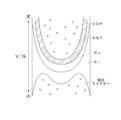
- FIG. 2 is a diagram showing a general relationship between V / G and the type and distribution of crystal defects.
- FIG. 3 is a flowchart showing a thermal donor generation rate measurement step.
- FIG. 4 is a flowchart showing a process of discriminating the presence / absence of a crystal defect region in the wafer and the type of crystal defect.
- FIG. 5 is a graph showing the relationship between the thermal donor generation rate and the thermal donor generation heat treatment time of the wafer samples A1 to A3 and B1 to B3.
- FIG. 1 is a flowchart for explaining a method of manufacturing a silicon wafer according to an embodiment of the present invention.
- FIG. 2 is a diagram showing a general relationship between V / G and the type and distribution of crystal defects.
- FIG. 3 is a flowchart showing a thermal donor generation rate measurement step.
- FIG. 4 is a flowchart showing
- FIG. 6 shows the result of determining the relationship between the thermal donor generation rate and the oxygen concentration in the OSF ring generation region, the region including void defects, and the defect-free region when the thermal donor generation heat treatment is performed at 450 ° C. for 4 hours. It is a graph which shows.
- FIG. 7 is a graph in which the thermal donor generation rate at each measurement point of the wafer without donor killer treatment in FIG. 6 is normalized by the thermal donor generation rate at the same measurement point of the wafer with donor killer treatment.
- FIG. 1 is a flowchart for explaining a method of manufacturing a silicon wafer according to an embodiment of the present invention.
- the silicon single crystal manufacturing method includes a crystal growth step (S11) for growing a silicon single crystal ingot by the CZ method, and a slicing step (S12) for cutting a silicon wafer from the silicon single crystal ingot. ), Thermal donor generation rate measurement step (S13Y, S14) performed when the evaluation of the crystal defect region of the silicon wafer is necessary, and the presence / absence of the crystal defect region and the type of crystal defect from the measurement result of the thermal donor generation rate A discriminating step (S15), and an adjusting step (S16Y, S17) for adjusting the growth conditions of the subsequent silicon single crystal ingot based on the discriminating result of the presence / absence of a crystal defect region and the type of crystal defect. Yes.
- the silicon single crystal manufacturing method includes a donor killer processing step (S18) performed when evaluation of a silicon wafer is unnecessary, and a product such as mirror polishing performed on the silicon wafer after the donor killer processing. And a processing step (S19).
- the kind and distribution of crystal defects contained in a silicon single crystal grown by the CZ method depend on the ratio V / G between the pulling speed V of the silicon single crystal and the temperature gradient G in the crystal in the pulling axis direction. Therefore, in order to control the crystal quality in the silicon single crystal, it is necessary to precisely control V / G. However, whether or not a silicon single crystal ingot (first silicon single crystal ingot) grown under a certain condition has a desired crystal quality cannot be known without actually evaluating the crystal quality.
- the presence / absence of a crystal defect region in the wafer cut out from the silicon single crystal ingot and the type of crystal defect are evaluated.
- this evaluation result is fed back to the subsequent silicon single crystal ingot (second silicon single crystal ingot) growing process.
- the crystal growth conditions such as the crystal pulling speed V are adjusted so that the desired crystal quality is obtained.
- FIG. 2 is a diagram showing a general relationship between V / G and the type and distribution of crystal defects.
- V / G when V / G is large, vacancies become excessive and void defects that are aggregates of vacancies are generated.
- a void defect is a crystal defect generally referred to as COP (Crystal Originated Particle).
- V / G when V / G is small, the number of interstitial silicon atoms becomes excessive, and dislocation clusters that are aggregates of interstitial silicon are generated. Therefore, in order to produce a single crystal containing neither COP nor dislocation clusters, V / G must be controlled in both the radial direction and the length direction (crystal growth direction) of the single crystal.
- an appropriate high temperature region is set in the chamber in order to keep the temperature gradient G in the radial direction within a predetermined range. Need to build.
- the intra-crystal temperature gradient G in the radial direction is controlled by a heat shield provided above the silicon melt, whereby an appropriate hot zone can be constructed near the solid-liquid interface.
- the temperature gradient G in the crystal in the length direction depends not only on the hot zone structure but also on the crystal pulling speed V, it is necessary to adjust the single crystal pulling speed V. At present, by strictly controlling the crystal pulling speed V, silicon single crystals having a diameter of 300 mm that do not contain COPs or dislocation clusters are mass-produced.
- a silicon wafer that does not contain COP and dislocation clusters pulled up by controlling V / G is never homogeneous, and includes a plurality of regions that behave differently when heat-treated. For example, there are three regions, an OSF region, a Pv region, and a Pi region, in descending order of V / G between a region where COP occurs and a region where dislocation clusters occur.
- the OSF region contains plate-like oxygen precipitates (OSF nuclei) in the as-grown state (the state in which no heat treatment is performed after single crystal growth), and is thermally oxidized at a high temperature of 1000 to 1200 ° C. This is a region where OSF occurs.
- the Pv region includes oxygen precipitation nuclei in an as-grown state, and is a region where oxygen precipitates are easily generated when two-stage heat treatment is performed at a low temperature and a high temperature (for example, 800 ° C. and 1000 ° C.).
- the Pi region is a region that hardly contains oxygen precipitation nuclei in an as-grown state and hardly generates oxygen precipitates even after heat treatment.
- the control of V / G is performed mainly by adjusting the pulling speed V.
- V / G is too large. Decrease the crystal pulling speed V.
- V / G is too small and the crystal pulling speed V is increased. .
- the time change of the thermal donor in the silicon wafer cut out from the ingot is measured.
- oxygen dissolved from the quartz crucible is usually 10 ⁇ 10 17 atoms / cm 3 (ASTM F-121, 1979). This oxygen causes crystal defects in the wafer and causes device characteristic defects.
- the wafer strength is increased to suppress deformation and heavy metals that cause device malfunction. It acts in a complicated manner, for example, by forming an oxygen precipitate having a gettering action for trapping the inside of the wafer.
- oxygen atoms in silicon are electrically neutral and do not affect their electrical resistance.
- a silicon single crystal produced by the CZ method is grown using a quartz crucible, it contains supersaturated oxygen in the crystal.
- heat-treated at a low temperature of around 450 ° C. several oxygen atoms gather to form an oxygen cluster. It is known to form and become a donor that emits electrons.
- the thermal donor formed by heat treatment at around 450 ° C. is affected by point defects, and the thermal donor generation rate differs depending on the difference in point defect concentration between the vacancy dominant region (COP region and OSF ring region) and the defect-free region. Therefore, in this embodiment, the presence / absence of a crystal defect region in the silicon wafer and the type of crystal defect are determined based on the generation rate of thermal donors generated in the silicon wafer.
- thermal donor generation rate measuring step (S14) two silicon wafers for evaluation that are continuously cut out from the ingot by the slicing step (S12) are prepared.
- the two evaluation wafers are preferably wafers cut out from the ingot by a wire saw and subjected to rough polishing.
- one of the wafers (first wafer) is subjected to a thermal donor generation heat treatment step without performing donor killer treatment in advance, and the other wafer (second wafer) is subjected to donor killer treatment in advance and then subjected to thermal treatment.
- a donor generation heat treatment is performed, and a thermal donor generation speed is obtained from a change in specific resistance before and after the thermal donor generation heat treatment of each of the first and second wafers.
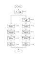
- FIG. 3 is a flowchart showing a thermal donor generation rate measurement step.
- the thermal donor generation rate measurement step (S14) includes a preparation step (S20) for preparing the first and second wafers in the as-grown state, and a ratio for measuring the specific resistance of the first wafer.
- a resistance measurement step (S21), a thermal donor generation heat treatment step (S22) for performing thermal donor generation heat treatment on the first wafer after the specific resistance measurement, and a specific resistance of the first wafer after the thermal donor generation heat treatment are measured.
- the thermal donor generation rate measuring step (S14) includes a step of performing donor killer processing on the second wafer (S25), a resistance measuring step of measuring the specific resistance of the second wafer after donor killer processing (S26), and A thermal donor generation heat treatment step (S27) for performing the same thermal donor generation heat treatment as that of the first wafer on the second wafer after the specific resistance measurement, and a specific resistance of the second wafer after the thermal donor generation heat treatment are measured.
- the temperature of the thermal donor-generated heat treatment is preferably 430 to 480 ° C, particularly preferably 450 ° C.
- the heat treatment time for generating the thermal donor is preferably 1 to 4 hours, more preferably 2 to 4 hours.
- the donor killer treatment is a short-time heat treatment performed in an inert gas atmosphere at 600 to 700 ° C., for example, and the heat treatment time is about 15 minutes, for example.
- the specific resistance in the silicon wafer surface can be measured by a so-called four-probe method. Based on the measured specific resistance, the carrier concentration is determined from the Irvine curve, the amount of thermal donor generation is determined based on the carrier concentration before and after the thermal donor generation heat treatment, and from the relationship between the thermal donor generation heat treatment time and the amount of thermal donor generation The thermal donor generation rate can be determined.
- a defect map in the radial direction of the silicon wafer can be created.
- FIG. 4 is a flowchart showing a process for discriminating the presence / absence of a crystal defect region in the wafer and the type of crystal defect.
- the ratio of the first thermal donor generation rate to the second thermal donor generation rate is calculated (S30).
- the value is 1.3 or more and less than 1.7
- the value is 1.7 or more and less than 1.9, it is a region including a void defect. It discriminate
- the silicon wafer evaluation method cuts out a silicon wafer from a silicon single crystal ingot grown by the CZ method and performs thermal donor generation heat treatment on the silicon wafer. Since the generation rate is measured and the presence or absence of the crystal defect region or the type of crystal defect is determined based on the generation rate of the thermal donor, the region including the OSF nucleus, the region including the void defect, or the non-defect region can be quickly determined. It can be easily determined.
- unlike the conventional evaluation method for example, it is not necessary to decorate copper, and evaluation can be performed with a relatively short time of low-temperature heat treatment. Existence and types of crystal defects can be evaluated.
- the silicon wafer manufacturing method measures the thermal donor generation rate of the evaluation silicon wafer cut out from the preceding silicon single crystal ingot, and based on the measurement result of the thermal donor generation rate, the evaluation silicon wafer Since the presence / absence of the crystal defect region or the type of the crystal defect is discriminated, and the growth condition of the subsequent silicon single crystal ingot is adjusted based on the discrimination result, the crystal growth condition can be easily optimized.
- the first and second silicon wafers cut from the silicon single crystal ingot in the thermal donor generation rate measuring step (S14) are prepared, and the donor killer process (S25) is performed on the second wafer.
- the thermal donor generation heat treatment (S27) is performed to calculate the second thermal donor generation rate.
- such a step of calculating the second thermal donor generation rate can be omitted.
- the other silicon wafer equivalent to the second silicon wafer is subjected to donor killer treatment and thermal donor generation heat treatment, and the second thermal donor generation rate calculated in advance is made into a database to generate the second thermal donor generation.
- the speed read from the database may be used, and only the first thermal donor generation speed may be measured to evaluate the presence / absence of a crystal defect region and the type of crystal defect.
- the effect of the type of crystal defects on the thermal donor generation rate was evaluated.
- a P-type silicon single crystal ingot having a diameter of 300 mm and a plane orientation (100) was grown by the CZ method.
- a silicon single crystal ingot was grown while controlling V / G so as to include the OSF ring generation region.
- the oxygen concentration of this silicon single crystal ingot was 5 ⁇ 10 17 to 20 ⁇ 10 17 atoms / cm 3 (ASTM F-121, 1979).
- samples A1 and B1 of two silicon wafers including the OSF ring generation region were obtained.
- the OSF ring generation region refers to a region where an OSF ring is generated after the evaluation heat treatment, and refers to a region including OSF nuclei in an as-grown state.
- a silicon single crystal ingot is grown under the same conditions as Samples A1 and B1 except that the V / G is controlled so that a void defect area is included, and the silicon single crystal ingot is sliced to obtain a void defect.
- Samples A2 and B2 of two silicon wafers including the region where the sapphire exists were obtained.
- a silicon single crystal ingot is produced under the same conditions as those of the samples A1 and B1 except that V / G is controlled so as to be a defect-free region, and this silicon single crystal ingot is sliced to form 2 Two silicon wafer samples A3 and B3 were obtained.
- a donor killer treatment was performed in a nitrogen atmosphere at 700 ° C. for 15 minutes.
- Samples A1 to A3 of silicon wafers prepared by processes without donor killer treatment (Examples 1 to 3) and samples B1 to B3 of silicon wafers prepared by processes with donor killer treatment (Comparative Examples 1 to 3), respectively.
- Thermal donor generation heat treatment was performed in a nitrogen atmosphere at 450 ° C. to generate a thermal donor.
- FIG. 5 is a graph showing the relationship between the thermal donor generation rate of the wafer samples A1 to A3 and B1 to B3 and the thermal donor generation heat treatment time.
- the horizontal axis represents the heat treatment time (h), and the vertical axis represents the thermal donor generation rate. (Cm ⁇ 3 / h) is shown respectively.
- this graph is summarized only for wafers that satisfy the condition of oxygen concentration of 11 ⁇ 10 17 atoms / cm 3 .
- the donor killer treatment is performed on the OSF ring generation region, the region including the void defect, and the non-defect region as compared with the case where the donor killer treatment is performed (samples B1, B2, and B3). None (samples A1, A2, A3) had a higher thermal donor generation rate.
- the thermal donor generation rate was the same in any region with the donor killer treatment, but without the donor killer treatment, the thermal donor generation rate increased in the order of the OSF ring generation region, the void-containing region, and the defect-free region. became.
- the thermal donor generation rate once increased and then decreased without the donor killer treatment.
- the thermal donor generation rate decreased, and after 16 hours, the thermal donor generation rate became the same under all conditions.
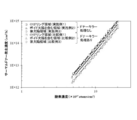
- FIG. 6 shows the result of determining the relationship between the thermal donor generation rate and the oxygen concentration in the OSF ring generation region, the region including void defects, and the defect-free region when the thermal donor generation heat treatment is performed at 450 ° C. for 4 hours.
- the horizontal axis represents the oxygen concentration ( ⁇ 10 17 atoms / cm 3 ), and the vertical axis represents the thermal donor generation rate (cm ⁇ 3 / h).
- the wafer with no donor killer treatment is the thermal donor at any oxygen concentration rather than the donor killer treatment (samples B1, B2, B3).
- the generation rate was great.
- the thermal donor generation rate was the same in all regions in the wafer with the donor killer process, but in the wafer without the donor killer process, the thermal donor was in the order of the OSF ring generation region, the region including the void defect, and the non-defect region. The generation rate has increased.
- FIG. 7 is a graph in which the thermal donor generation rate at each measurement point of the wafer without donor killer treatment is normalized with the thermal donor generation rate at the same measurement point of the wafer with donor killer treatment in the graph of FIG.
- the horizontal axis represents the oxygen concentration ( ⁇ 10 17 atoms / cm 3 ), and the vertical axis represents the thermal donor generation rate (standard value).
- the thermal donor generation rate in the defect-free region of the wafer without donor killer treatment was 1.3 times or more and less than 1.7 times the thermal donor generation rate of the wafer with donor killer treatment.
- the thermal donor generation rate in the region including the void defect of the wafer without donor killer treatment was 1.7 times or more and less than 1.9 times the thermal donor generation rate of the wafer with donor killer treatment.
- the thermal donor generation rate in the OSF ring generation region of the wafer without donor killer treatment was 1.9 times or more and less than 2.3 times the thermal donor generation rate of the wafer with donor killer treatment.
Landscapes
- Chemical & Material Sciences (AREA)
- Engineering & Computer Science (AREA)
- Crystallography & Structural Chemistry (AREA)
- Materials Engineering (AREA)
- Metallurgy (AREA)
- Organic Chemistry (AREA)
- Physics & Mathematics (AREA)
- Thermal Sciences (AREA)
- Crystals, And After-Treatments Of Crystals (AREA)
- Testing Or Measuring Of Semiconductors Or The Like (AREA)
Abstract
Description
S12 スライス工程
S13,S14 サーマルドナー発生速度測定工程
S15 判別工程
S16,S17 結晶育成条件調整工程
S20 ウェーハ準備工程
S21 第1のウェーハの比抵抗測定工程
S22 第1のウェーハのサーマルドナー発生熱処理工程
S23 第1のウェーハの比抵抗測定工程
S24 第1のサーマルドナー発生速度算出工程
S25 第2のウェーハのドナーキラー処理工程
S26 第2のウェーハの比抵抗測定工程
S27 第2のウェーハのサーマルドナー発生熱処理工程
S28 第2のウェーハの比抵抗測定工程
S29 第2のサーマルドナー発生速度算出工程
Claims (15)
- チョクラルスキー法によって育成されたシリコン単結晶インゴットから切り出したシリコンウェーハの評価方法であって、前記シリコンウェーハにサーマルドナー発生熱処理を施したときに発生するサーマルドナーの発生速度を測定し、当該サーマルドナーの発生速度に基づいて結晶欠陥領域の有無又は結晶欠陥の種類を判別することを特徴とするシリコンウェーハの評価方法。
- 前記シリコン単結晶インゴットから切り出した第1のシリコンウェーハが酸素クラスターを含む状態において前記サーマルドナー発生熱処理を施したときに前記第1のシリコンウェーハ上の第1の測定ポイントに発生するサーマルドナーの発生速度である第1のサーマルドナー発生速度を求め、
前記第1のシリコンウェーハと異なる第2のシリコンウェーハにドナーキラー処理及び前記サーマルドナー発生熱処理を順に施したときに前記第2のシリコンウェーハ上の第2の測定ポイントに発生するサーマルドナーの発生速度である第2のサーマルドナー発生速度を求め、
前記第2のサーマルドナー発生速度に対する第1のサーマルドナー発生速度の比であるサーマルドナー発生速度比に基づいて、前記第1のシリコンウェーハ上の前記第1の測定ポイントがOSF核を含む領域、ボイド欠陥を含む領域又は無欠陥領域のいずれに該当するかを判別する、請求項1に記載のシリコンウェーハの評価方法。 - 前記サーマルドナー発生速度比が第1の速度範囲内にある場合に、前記第1のシリコンウェーハ上の前記第1の測定ポイントが無欠陥領域であると判別し、
前記サーマルドナー発生速度比が前記第1の速度範囲よりも高い第2の速度範囲内にある場合に、前記第1のシリコンウェーハ上の前記第1の測定ポイントがボイド欠陥を含む領域であると判別し、
前記サーマルドナー発生速度比が前記第2の速度範囲よりも高い第3の速度範囲内にある場合に、前記第1のシリコンウェーハ上の前記第1の測定ポイントがOSF核を含む領域であると判別する、請求項2に記載のシリコンウェーハの評価方法。 - 前記サーマルドナー発生熱処理は、430℃以上480℃以下で2時間以上4時間以下の熱処理である、請求項1乃至3のいずれか一項に記載のシリコンウェーハの評価方法。
- 450℃で4時間の前記サーマルドナー発生熱処理を施したとき、前記サーマルドナー発生速度比が1.3以上1.7未満である場合に、前記第1のシリコンウェーハ上の前記第1の測定ポイントが無欠陥領域であると判別する、請求項2に記載のシリコンウェーハの評価方法。
- 450℃で4時間の前記サーマルドナー発生熱処理を施したとき、前記サーマルドナー発生速度比が1.7以上1.9未満である場合に、前記第1の測定ポイントがボイド欠陥を含む領域であると判別する、請求項2又は5に記載のシリコンウェーハの評価方法。
- 450℃で4時間の前記サーマルドナー発生熱処理を施したとき、前記サーマルドナー発生速度比が1.9以上2.3未満である場合に、前記第1の測定ポイントがOSF核を含む領域であると判別する、請求項2、5又は6に記載のシリコンウェーハの評価方法。
- 前記シリコンウェーハの径方向に沿って設けた複数の測定ポイントの各々において前記サーマルドナーの発生速度を測定することにより、前記シリコンウェーハの径方向の結晶欠陥マップを作成する、請求項1乃至7のいずれか一項に記載のシリコンウェーハの評価方法。
- 前記シリコンウェーハの比抵抗を測定し、前記比抵抗をもとにキャリア濃度をアービンカーブから求め、前記サーマルドナー発生熱処理前後のキャリア濃度をもとにサーマルドナー発生量を求め、前記サーマルドナー発生熱処理の時間と前記サーマルドナー発生量との関係から前記サーマルドナー発生速度を求める、請求項1乃至8のいずれか一項に記載のシリコンウェーハの評価方法。
- 第1のシリコン単結晶インゴットをチョクラルスキー法によって育成し、
前記第1のシリコン単結晶インゴットから切り出した評価用シリコンウェーハにサーマルドナー発生熱処理を施したときに発生するサーマルドナーの発生速度を測定し、当該サーマルドナーの発生速度の測定結果に基づいて前記評価用シリコンウェーハ中の結晶欠陥領域の有無又は結晶欠陥の種類を判別し、
前記第1のシリコン単結晶インゴットの育成条件及び前記評価用シリコンウェーハ中の結晶欠陥領域の有無又は結晶欠陥の種類の判別結果に基づいて、第2のシリコン単結晶インゴットの育成条件を調整し、前記第2のシリコン単結晶インゴットから製品用シリコンウェーハを切り出すことを特徴とするシリコンウェーハの製造方法。 - 前記第2のシリコン単結晶インゴットの育成条件を調整することによって、無欠陥領域を有する前記第2のシリコン単結晶インゴットを育成する、請求項10に記載のシリコンウェーハの製造方法。
- 前記第2のシリコン単結晶インゴットの育成条件を調整することによって、ボイド欠陥を含む領域を有する前記第2のシリコン単結晶インゴットを育成する、請求項10に記載のシリコンウェーハの製造方法。
- 前記第2のシリコン単結晶インゴットの育成条件を調整することによって、OSF核を含む領域を有する前記第2のシリコン単結晶インゴットを育成する、請求項10に記載のシリコンウェーハの製造方法。
- 前記第2のシリコン単結晶インゴットの育成条件として、前記第2のシリコン単結晶インゴットの引き上げ速度を調整する、請求項10乃至13のいずれか一項に記載のシリコンウェーハの製造方法。
- 前記製品用シリコンウェーハにドナーキラー処理を施す、請求項10乃至14のいずれか一項に記載のシリコンウェーハの製造方法。
Priority Applications (3)
| Application Number | Priority Date | Filing Date | Title |
|---|---|---|---|
| DE112017003486.8T DE112017003486B4 (de) | 2016-07-11 | 2017-02-23 | Verfahren zum evaluieren und herstellen von siliziumwafern |
| KR1020187036819A KR102180784B1 (ko) | 2016-07-11 | 2017-02-23 | 실리콘 웨이퍼의 평가 방법 및 제조 방법 |
| CN201780043227.6A CN109477241B (zh) | 2016-07-11 | 2017-02-23 | 硅晶片的评价方法及制造方法 |
Applications Claiming Priority (2)
| Application Number | Priority Date | Filing Date | Title |
|---|---|---|---|
| JP2016136639A JP6569613B2 (ja) | 2016-07-11 | 2016-07-11 | シリコンウェーハの評価方法及び製造方法 |
| JP2016-136639 | 2016-07-11 |
Publications (1)
| Publication Number | Publication Date |
|---|---|
| WO2018012019A1 true WO2018012019A1 (ja) | 2018-01-18 |
Family
ID=60951697
Family Applications (1)
| Application Number | Title | Priority Date | Filing Date |
|---|---|---|---|
| PCT/JP2017/006727 Ceased WO2018012019A1 (ja) | 2016-07-11 | 2017-02-23 | シリコンウェーハの評価方法及び製造方法 |
Country Status (6)
| Country | Link |
|---|---|
| JP (1) | JP6569613B2 (ja) |
| KR (1) | KR102180784B1 (ja) |
| CN (1) | CN109477241B (ja) |
| DE (1) | DE112017003486B4 (ja) |
| TW (1) | TWI631242B (ja) |
| WO (1) | WO2018012019A1 (ja) |
Families Citing this family (6)
| Publication number | Priority date | Publication date | Assignee | Title |
|---|---|---|---|---|
| JP6669133B2 (ja) * | 2017-06-23 | 2020-03-18 | 株式会社Sumco | シリコンウェーハのサーマルドナー生成挙動予測方法、シリコンウェーハの評価方法およびシリコンウェーハの製造方法 |
| JP6711327B2 (ja) * | 2017-07-18 | 2020-06-17 | 株式会社Sumco | シリコンウェーハ製造工程の評価方法およびシリコンウェーハの製造方法 |
| JP7336961B2 (ja) * | 2019-10-31 | 2023-09-01 | 信越化学工業株式会社 | 単結晶インゴットの製造方法及び単結晶ウエハの製造方法 |
| US11695048B2 (en) | 2020-04-09 | 2023-07-04 | Sumco Corporation | Silicon wafer and manufacturing method of the same |
| JP7613481B2 (ja) * | 2020-12-04 | 2025-01-15 | 株式会社Sumco | シリコン単結晶の育成方法 |
| CN119290973B (zh) * | 2024-12-10 | 2025-05-30 | 江西联创光电超导应用有限公司 | 一种晶体缺陷检测分析方法及系统 |
Citations (4)
| Publication number | Priority date | Publication date | Assignee | Title |
|---|---|---|---|---|
| JPH0982768A (ja) * | 1995-09-19 | 1997-03-28 | Hitachi Ltd | 半導体ウエハの評価方法 |
| WO2005071144A1 (ja) * | 2004-01-27 | 2005-08-04 | Komatsu Denshi Kinzoku Kabushiki Kaisha | シリコン単結晶中の酸素析出挙動予測方法、シリコン単結晶の製造パラメータ決定方法、シリコン単結晶中の酸素析出挙動予測用プログラムを記憶する記憶媒体 |
| JP2008545605A (ja) * | 2005-05-19 | 2008-12-18 | エムイーエムシー・エレクトロニック・マテリアルズ・インコーポレイテッド | 高抵抗率シリコン構造体およびその製造方法 |
| JP2016500641A (ja) * | 2012-10-23 | 2016-01-14 | コミサリア ア レネルジー アトミック エ オ ゼネルジー アルテルナティブCommissariat Al’Energie Atomique Et Aux Energiesalternatives | 一様な抵抗を有するドーピングされたシリコンインゴットを形成する方法 |
Family Cites Families (11)
| Publication number | Priority date | Publication date | Assignee | Title |
|---|---|---|---|---|
| JPH04134840A (ja) * | 1990-09-27 | 1992-05-08 | Kawasaki Steel Corp | シリコンウェーハの重金属不純物エネルギー準位の測定方法 |
| JP3341378B2 (ja) * | 1993-08-25 | 2002-11-05 | 富士通株式会社 | シリコン結晶中の水素濃度測定方法及びシリコン結晶の製造方法 |
| JP3085146B2 (ja) | 1995-05-31 | 2000-09-04 | 住友金属工業株式会社 | シリコン単結晶ウェーハおよびその製造方法 |
| KR100237829B1 (ko) * | 1997-02-06 | 2000-01-15 | 윤종용 | 웨이퍼의 결함 분석방법 |
| JP2001081000A (ja) * | 1999-09-08 | 2001-03-27 | Shin Etsu Handotai Co Ltd | シリコン単結晶の結晶欠陥評価方法 |
| JP2007235153A (ja) * | 2002-04-26 | 2007-09-13 | Sumco Corp | 高抵抗シリコンウエーハ及びその製造方法 |
| JP2006054350A (ja) * | 2004-08-12 | 2006-02-23 | Komatsu Electronic Metals Co Ltd | 窒素ドープシリコンウェーハとその製造方法 |
| FR2964459B1 (fr) * | 2010-09-02 | 2012-09-28 | Commissariat Energie Atomique | Procede de cartographie de la concentration en oxygene |
| KR101246493B1 (ko) * | 2011-07-08 | 2013-04-01 | 주식회사 엘지실트론 | 웨이퍼의 결함 평가방법 |
| KR101759876B1 (ko) * | 2015-07-01 | 2017-07-31 | 주식회사 엘지실트론 | 웨이퍼 및 웨이퍼 결함 분석 방법 |
| CN105332061A (zh) * | 2015-11-17 | 2016-02-17 | 阳光能源(青海)有限公司 | 一种消除单晶棒氧施主效应对电阻率影响的热处理工艺 |
-
2016
- 2016-07-11 JP JP2016136639A patent/JP6569613B2/ja active Active
-
2017
- 2017-02-23 KR KR1020187036819A patent/KR102180784B1/ko active Active
- 2017-02-23 CN CN201780043227.6A patent/CN109477241B/zh active Active
- 2017-02-23 DE DE112017003486.8T patent/DE112017003486B4/de active Active
- 2017-02-23 WO PCT/JP2017/006727 patent/WO2018012019A1/ja not_active Ceased
- 2017-04-06 TW TW106111517A patent/TWI631242B/zh active
Patent Citations (4)
| Publication number | Priority date | Publication date | Assignee | Title |
|---|---|---|---|---|
| JPH0982768A (ja) * | 1995-09-19 | 1997-03-28 | Hitachi Ltd | 半導体ウエハの評価方法 |
| WO2005071144A1 (ja) * | 2004-01-27 | 2005-08-04 | Komatsu Denshi Kinzoku Kabushiki Kaisha | シリコン単結晶中の酸素析出挙動予測方法、シリコン単結晶の製造パラメータ決定方法、シリコン単結晶中の酸素析出挙動予測用プログラムを記憶する記憶媒体 |
| JP2008545605A (ja) * | 2005-05-19 | 2008-12-18 | エムイーエムシー・エレクトロニック・マテリアルズ・インコーポレイテッド | 高抵抗率シリコン構造体およびその製造方法 |
| JP2016500641A (ja) * | 2012-10-23 | 2016-01-14 | コミサリア ア レネルジー アトミック エ オ ゼネルジー アルテルナティブCommissariat Al’Energie Atomique Et Aux Energiesalternatives | 一様な抵抗を有するドーピングされたシリコンインゴットを形成する方法 |
Also Published As
| Publication number | Publication date |
|---|---|
| TW201809375A (zh) | 2018-03-16 |
| CN109477241B (zh) | 2021-05-18 |
| KR102180784B1 (ko) | 2020-11-19 |
| JP2018008832A (ja) | 2018-01-18 |
| DE112017003486T5 (de) | 2019-04-04 |
| CN109477241A (zh) | 2019-03-15 |
| KR20190009354A (ko) | 2019-01-28 |
| TWI631242B (zh) | 2018-08-01 |
| JP6569613B2 (ja) | 2019-09-04 |
| DE112017003486B4 (de) | 2025-10-02 |
Similar Documents
| Publication | Publication Date | Title |
|---|---|---|
| JP6569613B2 (ja) | シリコンウェーハの評価方法及び製造方法 | |
| KR100461893B1 (ko) | 실리콘 웨이퍼 및 이것에 사용되는 실리콘 단결정의제조방법 | |
| US8231852B2 (en) | Silicon wafer and method for producing the same | |
| JP6724142B2 (ja) | 均質な径方向の酸素変化量を有するシリコンウェハ | |
| JP2001500468A (ja) | 低欠陥密度の自己格子間物優勢シリコン | |
| KR101997561B1 (ko) | 실리콘 단결정봉의 제조방법 | |
| CN101024895A (zh) | 外延晶片以及制造外延晶片的方法 | |
| US20110263126A1 (en) | Method for manufacturing a silicon wafer | |
| JP5163459B2 (ja) | シリコン単結晶の育成方法及びシリコンウェーハの検査方法 | |
| KR101895817B1 (ko) | 실리콘 웨이퍼 및 그 제조 방법 | |
| JP2003055088A (ja) | シリコン半導体基板およびその製造方法 | |
| US6261362B1 (en) | Silicon epitaxial wafer manufacturing method | |
| JP2001217251A (ja) | シリコンウェーハの熱処理方法 | |
| JP4131077B2 (ja) | シリコンウェーハの製造方法 | |
| JP2001151597A (ja) | 点欠陥の凝集体が存在しないシリコンウェーハの製造方法 | |
| JP2008066357A (ja) | シリコン単結晶ウエーハおよびシリコン単結晶ウエーハの製造方法 | |
| KR100445190B1 (ko) | 단결정 실리콘 잉곳 제조 방법 | |
| KR100389250B1 (ko) | 실리콘 웨이퍼 및 그 제조 방법 | |
| JP2001102385A (ja) | 点欠陥の凝集体が存在しないシリコンウェーハ | |
| JP3452042B2 (ja) | シリコンウェーハの製造方法 | |
| JP2010116271A (ja) | シリコン単結晶の育成方法及びシリコン単結晶インゴット | |
| JP2002134517A (ja) | シリコンウェーハの熱処理方法 | |
| JP2004189584A (ja) | シリコン単結晶インゴットの点欠陥分布を測定する方法 | |
| JP2010155748A (ja) | アニ―ルウェハの製造方法 | |
| JP2021098623A (ja) | 単結晶シリコンウェーハの酸化膜耐圧の評価方法 |
Legal Events
| Date | Code | Title | Description |
|---|---|---|---|
| 121 | Ep: the epo has been informed by wipo that ep was designated in this application |
Ref document number: 17827154 Country of ref document: EP Kind code of ref document: A1 |
|
| ENP | Entry into the national phase |
Ref document number: 20187036819 Country of ref document: KR Kind code of ref document: A |
|
| 122 | Ep: pct application non-entry in european phase |
Ref document number: 17827154 Country of ref document: EP Kind code of ref document: A1 |
|
| WWG | Wipo information: grant in national office |
Ref document number: 112017003486 Country of ref document: DE |