WO2018008364A1 - 光学装置、露光装置及び物品の製造方法 - Google Patents
光学装置、露光装置及び物品の製造方法 Download PDFInfo
- Publication number
- WO2018008364A1 WO2018008364A1 PCT/JP2017/022311 JP2017022311W WO2018008364A1 WO 2018008364 A1 WO2018008364 A1 WO 2018008364A1 JP 2017022311 W JP2017022311 W JP 2017022311W WO 2018008364 A1 WO2018008364 A1 WO 2018008364A1
- Authority
- WO
- WIPO (PCT)
- Prior art keywords
- optical device
- mirror
- permanent magnet
- shape
- base plate
- Prior art date
- Legal status (The legal status is an assumption and is not a legal conclusion. Google has not performed a legal analysis and makes no representation as to the accuracy of the status listed.)
- Ceased
Links
Images


Classifications
-
- G—PHYSICS
- G02—OPTICS
- G02B—OPTICAL ELEMENTS, SYSTEMS OR APPARATUS
- G02B5/00—Optical elements other than lenses
- G02B5/08—Mirrors
- G02B5/10—Mirrors with curved faces
-
- G—PHYSICS
- G02—OPTICS
- G02B—OPTICAL ELEMENTS, SYSTEMS OR APPARATUS
- G02B7/00—Mountings, adjusting means, or light-tight connections, for optical elements
-
- G—PHYSICS
- G02—OPTICS
- G02B—OPTICAL ELEMENTS, SYSTEMS OR APPARATUS
- G02B7/00—Mountings, adjusting means, or light-tight connections, for optical elements
- G02B7/18—Mountings, adjusting means, or light-tight connections, for optical elements for prisms; for mirrors
- G02B7/182—Mountings, adjusting means, or light-tight connections, for optical elements for prisms; for mirrors for mirrors
- G02B7/185—Mountings, adjusting means, or light-tight connections, for optical elements for prisms; for mirrors for mirrors with means for adjusting the shape of the mirror surface
-
- G—PHYSICS
- G03—PHOTOGRAPHY; CINEMATOGRAPHY; ANALOGOUS TECHNIQUES USING WAVES OTHER THAN OPTICAL WAVES; ELECTROGRAPHY; HOLOGRAPHY
- G03F—PHOTOMECHANICAL PRODUCTION OF TEXTURED OR PATTERNED SURFACES, e.g. FOR PRINTING, FOR PROCESSING OF SEMICONDUCTOR DEVICES; MATERIALS THEREFOR; ORIGINALS THEREFOR; APPARATUS SPECIALLY ADAPTED THEREFOR
- G03F7/00—Photomechanical, e.g. photolithographic, production of textured or patterned surfaces, e.g. printing surfaces; Materials therefor, e.g. comprising photoresists; Apparatus specially adapted therefor
- G03F7/20—Exposure; Apparatus therefor
Definitions
- the present invention relates to an optical apparatus, an exposure apparatus, and a method of manufacturing an article.
- Patent Document 1 discloses a technique of correcting a shape error from an ideal shape (reference shape) generated by screw fastening at the time of mirror attachment by driving an electromagnet actuator.
- the heat generated from the electromagnet actuator causes unintended deformation of the mirror and new optical Aberrations can occur.
- An object of the present invention is, for example, to provide an optical device capable of correcting the shape with high accuracy by suppressing heat generation accompanying the shape correction of the optical element.
- an optical device that deforms a reflective surface of an optical element, and a base plate disposed apart from the surface on the opposite side of the reflective surface
- a correction unit including: a first permanent magnet attached to the surface opposite to the reflecting surface; and a second permanent magnet disposed at a position facing the first permanent magnet of the base plate The correction unit corrects the shape of the reflecting surface by a repulsive force or an attractive force generated by the first permanent magnet and the second permanent magnet.
- an optical device capable of correcting the shape with high accuracy by suppressing the heat generation accompanying the shape correction of the optical element.
- FIG. 1 is a view showing a schematic configuration of an exposure apparatus according to a first embodiment. It is a sectional view showing a schematic structure of an optical device concerning a 1st embodiment.
- FIG. 1 is a front view showing a schematic configuration of an optical device according to a first embodiment. It is sectional drawing which shows schematic structure of the optical apparatus which concerns on 2nd Embodiment. It is a front view which shows schematic structure of the optical apparatus which concerns on 2nd Embodiment.
- FIG. 1 is a view showing a schematic configuration of an exposure apparatus.
- the exposure apparatus 50 includes an illumination optical system IL, a projection optical system UM, a mask stage MS which can move while holding the mask 55, and a substrate stage PS which can move while holding the substrate 56.
- the exposure apparatus 50 also includes a control unit 51 that controls the process of exposing the substrate 56.
- the light emitted from the light source (not shown) included in the illumination optical system IL forms, for example, an arc-shaped illumination area long in the Y direction on the mask 55 by a slit (not shown) included in the illumination optical system IL. can do.
- the mask 55 and the substrate 56 are held by the mask stage MS and the substrate stage PS, respectively, and are at a substantially optically conjugate position (the position of the object plane and the image plane of the projection optical system UM) via the projection optical system UM. Be placed.
- the projection optical system UM has a predetermined projection magnification (for example, 1 ⁇ 2), and projects the pattern formed on the mask 55 onto the substrate 56.
- the mask stage MS and the substrate stage PS are scanned in a direction parallel to the object surface of the projection optical system UM (for example, the X direction in FIG. 1) at a speed ratio corresponding to the projection magnification of the projection optical system UM. Thereby, the pattern formed on the mask 55 can be transferred to the substrate 56.
- the projection optical system UM is configured to include, for example, a plane mirror 52, a mirror 1 which is a concave mirror, and a convex mirror 54, as shown in FIG.
- the exposure light emitted from the illumination optical system IL and transmitted through the mask 55 has its optical path bent by the first surface 52 a of the plane mirror 52 and enters the first surface 1 a 1 of the mirror 1.
- the exposure light reflected on the first surface 1 a 1 of the mirror 1 is reflected on the convex mirror 54 and is incident on the second surface 1 a 2 of the mirror 1.
- the exposure light reflected by the second surface 1 a 2 of the mirror 1 is bent along the optical path by the second surface 52 b of the plane mirror 52 and forms an image on the substrate 56.
- the optical device 10 is, for example, a large aperture concave mirror device used in a reflection mirror type exposure device.
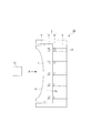
- FIG. 2 is a cross-sectional view of the optical device.
- the optical device 10 includes a mirror 1, a base plate 5, and a plurality of shape error correction units (correction units) 2.
- the mirror 1 is an optical element having a reflective surface 1 a that reflects light and a back surface 1 b that is the surface opposite to the reflective surface.
- the mirror 1 is fixed to the base plate 5 via a fixing member 6.
- the base plate 5 is spaced apart on the back surface 1b.
- the correction unit 2 is disposed between the mirror 1 and the base plate 5, and the first permanent magnet (mirror side magnet) 3 on the mirror side disposed on the back surface 1 b of the mirror 1 and the base side disposed on the opposing base plate 5
- the correction unit 2 can generate a suction force or a repulsive force by inverting and installing the polarity of the base-side magnet 4 facing the mirror-side magnet 3. Further, by adjusting the inter-magnet distance between the mirror-side magnet 3 and the base-side magnet 4 facing the mirror-side magnet 3 using the adjustment mechanism 13, the amount of generated force can be adjusted.
- the distance between the magnets is adjusted by adjusting the position where the base-side magnet 4 is disposed by the adjustment mechanism 13.
- the present invention is not limited to this, and the attraction force and the repulsive force may be switched by changing the polarity of the mirror-side magnet 3.
- the shape of the reflective surface 1a of the mirror 1 is measured using the measurement unit 12, and the direction and amount of force (shape error) required to correct the error of the shape are calculated.
- the measurement unit 12 is configured of a measurement instrument that measures the shape of the reflection surface 1 a of the mirror 1, such as a laser interferometer or a Shack-Hartmann sensor.
- the polarity of the base-side magnet 4 of each correction unit 2 is selected according to the positive / negative (concave / convex) of the shape error indicating the direction and amount of force required to correct the error of the shape, and either attraction or repulsion
- the distance between the mirror side magnet 3 and the base side magnet 4 of each correction unit 2 is adjusted by the adjustment mechanism 13 to adjust the generated force.
- the plurality of correction units 2 partially generate tensile stress or compressive stress on the mirror 1. Therefore, the mirror surface 1a is partially elastically deformed according to the tensile stress or the compressive stress, and the shape error of the mirror surface 1a is corrected.
- the shape error of the mirror 1 can be corrected without the heat generated by the shape correction mechanism due to the correction unit 2 configured by the permanent magnet.
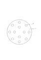
- FIG. 3 is a front view looking at the optical device 10 in the direction of arrow A in FIG.
- the correction units 2 are disposed at four locations at 90 ° intervals on the same circumference, and at eight locations at 45 ° intervals on another further outer circumference.
- the arrangement of the correction unit 2 is not limited to this, and the number and arrangement may be changed according to the optical aberration to be corrected.
- the optical device of this embodiment can be variously modified without departing from the scope of the invention.
- the number, arrangement, and the like of the correction units 2 can be set arbitrarily.
- the outer peripheral portion of the mirror 1 is fixed to the base plate 5 by the fixing member 6, any part of the mirror 1 may be fixed to the base plate 5 by the fixing member 6.
- means such as screws or adhesion may be adopted for connecting the mirror 1 and the base plate 5.
- a spherical mirror having a circular concave surface is used as the mirror 1
- the present invention is not limited thereto.
- a flat mirror or a spherical mirror having a convex surface may be used as the mirror 1.
- the measuring unit 12 has been described by way of example of a sensor that measures the surface shape, but a sensor array configured of a plurality of displacement sensors that measure a plurality of positions of the mirror 1 may be used.
- FIG. 4 is a cross-sectional view of the optical device according to the second embodiment.
- the optical device 20 is, for example, a large-diameter concave mirror device used for a reflection mirror type exposure device, and can be applied to the mirror 1 in the exposure device of FIG.
- the optical device 20 corrects, for example, the optical aberration of the projection optical system, the magnification and distortion of the projection image, and the focus by deforming the reflection surface 1a of the mirror 1 included in the projection optical system of the exposure apparatus.
- the optical device 20 includes a mirror 1, a base plate 5, a plurality of actuators 7, a plurality of displacement sensors 14, and a control unit 11.
- the control unit 11 includes a CPU, a memory, and the like, and controls the displacement sensor 14 and the plurality of actuators 7.
- the actuator 7 is disposed between the mirror 1 and the base plate 5 and applies a force to the back surface 1 b of the mirror 1.
- the actuator 7 has a mover magnet 8 fixed to the back surface 1 b and a stator coil 9 fixed to the base plate 5.
- the displacement sensor 14 measures the distance to the back surface 1 b of the mirror 1. Based on the measurement value of the displacement sensor 14, the control command value of the actuator 7 is calculated by the control unit 11, and a desired force is generated. Thereby, the reflection surface 1a of the mirror 1 can be deformed at high speed and with high accuracy, and optical aberration in the projection optical system UM can be corrected in real time and with high accuracy.
- the optical device 20 also has a correction unit 2.
- the correction unit 2 is arranged between the mirror 1 and the base plate 5 and is composed of the mirror side magnet 3 disposed on the back surface 1 b of the mirror 1 and the base side magnet 4 disposed on the base plate 5 facing the mirror 1.
- the shape correction method by the correction unit 2 is the same as that of the first embodiment.
- the measurement unit 12 may be used as in the first embodiment, or the displacement sensor 14 may be used.
- the processing accuracy required for the mirror 1 is high, but the processing error can be corrected by the correction unit 2 Therefore, processing time and processing cost of the mirror 1 can be suppressed.
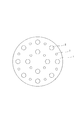
- FIG. 5 is a front view looking at the optical device 20 in the direction of arrow B in FIG.
- the correction unit 2 and the actuator 7 are respectively arranged at four locations at 90 ° intervals on the same circumference, and another 8 locations at 45 ° intervals on another outer circumference. ing.
- the arrangement of the arrangement of the correction unit 2 and the actuator 7 is not limited to this, and the number and arrangement may be changed according to the optical aberration to be corrected.
- the central portion of the mirror 1 is fixed to the base plate 5 by the fixing member 6, but any portion of the mirror 1 may be fixed to the base plate 5 by the fixing member 6.
- a non-contact type actuator such as a voice coil motor (VCM) including the mover magnet 8 and the stator coil 9 not in contact with each other, or a displacement actuator such as a piezoelectric element may be used.
- VCM voice coil motor
- a displacement actuator such as a piezoelectric element
- the optical device As described above, by performing the shape correction of the optical device with the correction unit configured by the permanent magnet, without generating heat accompanying the shape correction as shown in the first embodiment, or the second embodiment As shown in the above, it is possible to suppress heat generation and perform shape correction with high accuracy.
- an apparatus to which the optical device according to the above embodiment can be applied forms, for example, a latent image pattern of resist on a substrate by irradiation with EUV light.
- lithographic apparatus There is a lithographic apparatus.
- the present invention is applicable to a laser processing apparatus, a fundus imaging apparatus, a telescope, and the like.
- the method of manufacturing an article according to the present embodiment is suitable, for example, for manufacturing an article such as a microdevice such as a semiconductor device or an element having a microstructure.
- a latent image pattern is formed in the step of forming a latent image pattern on the photosensitive agent applied to the substrate using the above-described exposure apparatus (the step of exposing the substrate) And developing the substrate.
- a manufacturing method includes other known steps (oxidation, film formation, deposition, doping, planarization, etching, resist stripping, dicing, bonding, packaging, etc.).
- the method of manufacturing an article according to the present embodiment is advantageous in at least one of the performance, quality, productivity, and production cost of an article, as compared to the conventional method.
Landscapes
- Physics & Mathematics (AREA)
- General Physics & Mathematics (AREA)
- Optics & Photonics (AREA)
- Exposure And Positioning Against Photoresist Photosensitive Materials (AREA)
- Optical Elements Other Than Lenses (AREA)
- Mounting And Adjusting Of Optical Elements (AREA)
Priority Applications (2)
| Application Number | Priority Date | Filing Date | Title |
|---|---|---|---|
| CN201780040473.6A CN109416457B (zh) | 2016-07-06 | 2017-06-16 | 光学装置、曝光装置及物品的制造方法 |
| KR1020197002601A KR102165797B1 (ko) | 2016-07-06 | 2017-06-16 | 광학 장치, 노광 장치 및 물품의 제조 방법 |
Applications Claiming Priority (2)
| Application Number | Priority Date | Filing Date | Title |
|---|---|---|---|
| JP2016-134000 | 2016-07-06 | ||
| JP2016134000A JP6929024B2 (ja) | 2016-07-06 | 2016-07-06 | 光学装置、露光装置及び物品の製造方法 |
Publications (1)
| Publication Number | Publication Date |
|---|---|
| WO2018008364A1 true WO2018008364A1 (ja) | 2018-01-11 |
Family
ID=60912605
Family Applications (1)
| Application Number | Title | Priority Date | Filing Date |
|---|---|---|---|
| PCT/JP2017/022311 Ceased WO2018008364A1 (ja) | 2016-07-06 | 2017-06-16 | 光学装置、露光装置及び物品の製造方法 |
Country Status (4)
| Country | Link |
|---|---|
| JP (1) | JP6929024B2 (enExample) |
| KR (1) | KR102165797B1 (enExample) |
| CN (1) | CN109416457B (enExample) |
| WO (1) | WO2018008364A1 (enExample) |
Families Citing this family (2)
| Publication number | Priority date | Publication date | Assignee | Title |
|---|---|---|---|---|
| CN109932804B (zh) * | 2019-03-04 | 2021-06-01 | 杭州电子科技大学 | 一种小口径轻型反射镜的柔性记忆合金支撑装置 |
| JP2022022912A (ja) * | 2020-07-10 | 2022-02-07 | キヤノン株式会社 | 露光装置および物品製造方法 |
Citations (5)
| Publication number | Priority date | Publication date | Assignee | Title |
|---|---|---|---|---|
| JP2005004146A (ja) * | 2002-07-03 | 2005-01-06 | Nikon Corp | 反射光学素子及び露光装置 |
| JP2011119551A (ja) * | 2009-12-04 | 2011-06-16 | Nikon Corp | 光学部材変形装置、光学系、露光装置、デバイスの製造方法 |
| JP2011530721A (ja) * | 2008-08-14 | 2011-12-22 | アルパオ | フォースアクチュエータ及び分散剛性を有する可変ミラー |
| JP2014147169A (ja) * | 2013-01-28 | 2014-08-14 | Mitsubishi Electric Corp | 形状可変鏡装置 |
| JP2015126037A (ja) * | 2013-12-25 | 2015-07-06 | キヤノン株式会社 | 光学装置、投影光学系、露光装置、および物品の製造方法 |
Family Cites Families (9)
| Publication number | Priority date | Publication date | Assignee | Title |
|---|---|---|---|---|
| JPH02101402A (ja) | 1988-10-11 | 1990-04-13 | Omron Tateisi Electron Co | 反射鏡装置 |
| US7589822B2 (en) * | 2004-02-02 | 2009-09-15 | Nikon Corporation | Stage drive method and stage unit, exposure apparatus, and device manufacturing method |
| JP2008310925A (ja) * | 2007-06-18 | 2008-12-25 | Sony Corp | 変形可能ミラー装置、光ピックアップ、光学ドライブ装置 |
| FR2923301B1 (fr) * | 2007-11-02 | 2010-09-17 | Ujf Filiale | Miroir deformable a raideur repartie,outil et procede pour realiser un tel miroir |
| CN103891114B (zh) * | 2011-10-27 | 2018-01-02 | 不列颠哥伦比亚大学 | 位移装置及其制造、使用和控制方法 |
| JP2015050353A (ja) * | 2013-09-02 | 2015-03-16 | キヤノン株式会社 | 光学装置、投影光学系、露光装置、並びに物品の製造方法 |
| JP2015065246A (ja) * | 2013-09-24 | 2015-04-09 | キヤノン株式会社 | 光学装置、光学系、露光装置及び物品の製造方法 |
| JP6168957B2 (ja) * | 2013-09-30 | 2017-07-26 | キヤノン株式会社 | 光学装置、投影光学系、露光装置および物品の製造方法 |
| JP2016092366A (ja) * | 2014-11-11 | 2016-05-23 | キヤノン株式会社 | 光学装置、投影光学系、露光装置、および物品の製造方法 |
-
2016
- 2016-07-06 JP JP2016134000A patent/JP6929024B2/ja not_active Expired - Fee Related
-
2017
- 2017-06-16 CN CN201780040473.6A patent/CN109416457B/zh not_active Expired - Fee Related
- 2017-06-16 KR KR1020197002601A patent/KR102165797B1/ko not_active Expired - Fee Related
- 2017-06-16 WO PCT/JP2017/022311 patent/WO2018008364A1/ja not_active Ceased
Patent Citations (5)
| Publication number | Priority date | Publication date | Assignee | Title |
|---|---|---|---|---|
| JP2005004146A (ja) * | 2002-07-03 | 2005-01-06 | Nikon Corp | 反射光学素子及び露光装置 |
| JP2011530721A (ja) * | 2008-08-14 | 2011-12-22 | アルパオ | フォースアクチュエータ及び分散剛性を有する可変ミラー |
| JP2011119551A (ja) * | 2009-12-04 | 2011-06-16 | Nikon Corp | 光学部材変形装置、光学系、露光装置、デバイスの製造方法 |
| JP2014147169A (ja) * | 2013-01-28 | 2014-08-14 | Mitsubishi Electric Corp | 形状可変鏡装置 |
| JP2015126037A (ja) * | 2013-12-25 | 2015-07-06 | キヤノン株式会社 | 光学装置、投影光学系、露光装置、および物品の製造方法 |
Also Published As
| Publication number | Publication date |
|---|---|
| CN109416457A (zh) | 2019-03-01 |
| KR102165797B1 (ko) | 2020-10-14 |
| CN109416457B (zh) | 2021-09-17 |
| KR20190020139A (ko) | 2019-02-27 |
| JP2018005068A (ja) | 2018-01-11 |
| JP6929024B2 (ja) | 2021-09-01 |
Similar Documents
| Publication | Publication Date | Title |
|---|---|---|
| JP6336274B2 (ja) | 光学装置、投影光学系、露光装置、および物品の製造方法 | |
| JP6168957B2 (ja) | 光学装置、投影光学系、露光装置および物品の製造方法 | |
| US9557560B2 (en) | Mirror unit and exposure apparatus | |
| TWI631430B (zh) | Optical device, projection optical system, exposure device, and article manufacturing method | |
| US10884236B2 (en) | Optical device, projection optical system, exposure apparatus using the same, and method for manufacturing article | |
| CN109416457B (zh) | 光学装置、曝光装置及物品的制造方法 | |
| JP2016092309A (ja) | 光学装置、投影光学系、露光装置、および物品の製造方法 | |
| JP6808381B2 (ja) | 保持装置、投影光学系、露光装置、および物品製造方法 | |
| CN108227401B (zh) | 光学装置、曝光装置以及物品的制造方法 | |
| JP2008112756A (ja) | 光学素子駆動装置及びその制御方法、露光装置、並びにデバイス製造方法 | |
| KR102230464B1 (ko) | 광학 소자, 노광 장치, 및 물품의 제조 방법 | |
| JP6736371B2 (ja) | 位置調整機構、露光装置及び物品の製造方法 | |
| JP7759430B1 (ja) | 露光装置、露光方法及び物品の製造方法 | |
| US20230060389A1 (en) | Driving apparatus, exposure apparatus, and article manufacturing method | |
| JP7033997B2 (ja) | 露光装置、および物品の製造方法 | |
| JP2018066959A (ja) | 光学装置、投影光学系、露光装置及び物品の製造方法 | |
| JP6853659B2 (ja) | 決定方法、光学装置、投影光学系、露光装置及び物品の製造方法 | |
| CN119487448A (zh) | 光学组件、用于半导体光刻的投射曝光系统及方法 |
Legal Events
| Date | Code | Title | Description |
|---|---|---|---|
| 121 | Ep: the epo has been informed by wipo that ep was designated in this application |
Ref document number: 17823971 Country of ref document: EP Kind code of ref document: A1 |
|
| NENP | Non-entry into the national phase |
Ref country code: DE |
|
| ENP | Entry into the national phase |
Ref document number: 20197002601 Country of ref document: KR Kind code of ref document: A |
|
| 122 | Ep: pct application non-entry in european phase |
Ref document number: 17823971 Country of ref document: EP Kind code of ref document: A1 |