WO2018008364A1 - Optical device, exposure device, and method for manufacturing article - Google Patents
Optical device, exposure device, and method for manufacturing article Download PDFInfo
- Publication number
- WO2018008364A1 WO2018008364A1 PCT/JP2017/022311 JP2017022311W WO2018008364A1 WO 2018008364 A1 WO2018008364 A1 WO 2018008364A1 JP 2017022311 W JP2017022311 W JP 2017022311W WO 2018008364 A1 WO2018008364 A1 WO 2018008364A1
- Authority
- WO
- WIPO (PCT)
- Prior art keywords
- optical device
- mirror
- permanent magnet
- shape
- base plate
- Prior art date
Links
Images


Classifications
-
- G—PHYSICS
- G02—OPTICS
- G02B—OPTICAL ELEMENTS, SYSTEMS OR APPARATUS
- G02B5/00—Optical elements other than lenses
- G02B5/08—Mirrors
- G02B5/10—Mirrors with curved faces
-
- G—PHYSICS
- G02—OPTICS
- G02B—OPTICAL ELEMENTS, SYSTEMS OR APPARATUS
- G02B7/00—Mountings, adjusting means, or light-tight connections, for optical elements
-
- G—PHYSICS
- G02—OPTICS
- G02B—OPTICAL ELEMENTS, SYSTEMS OR APPARATUS
- G02B7/00—Mountings, adjusting means, or light-tight connections, for optical elements
- G02B7/18—Mountings, adjusting means, or light-tight connections, for optical elements for prisms; for mirrors
- G02B7/182—Mountings, adjusting means, or light-tight connections, for optical elements for prisms; for mirrors for mirrors
- G02B7/185—Mountings, adjusting means, or light-tight connections, for optical elements for prisms; for mirrors for mirrors with means for adjusting the shape of the mirror surface
-
- G—PHYSICS
- G03—PHOTOGRAPHY; CINEMATOGRAPHY; ANALOGOUS TECHNIQUES USING WAVES OTHER THAN OPTICAL WAVES; ELECTROGRAPHY; HOLOGRAPHY
- G03F—PHOTOMECHANICAL PRODUCTION OF TEXTURED OR PATTERNED SURFACES, e.g. FOR PRINTING, FOR PROCESSING OF SEMICONDUCTOR DEVICES; MATERIALS THEREFOR; ORIGINALS THEREFOR; APPARATUS SPECIALLY ADAPTED THEREFOR
- G03F7/00—Photomechanical, e.g. photolithographic, production of textured or patterned surfaces, e.g. printing surfaces; Materials therefor, e.g. comprising photoresists; Apparatus specially adapted therefor
- G03F7/20—Exposure; Apparatus therefor
Definitions
- the present invention relates to an optical apparatus, an exposure apparatus, and a method of manufacturing an article.
- Patent Document 1 discloses a technique of correcting a shape error from an ideal shape (reference shape) generated by screw fastening at the time of mirror attachment by driving an electromagnet actuator.
- the heat generated from the electromagnet actuator causes unintended deformation of the mirror and new optical Aberrations can occur.
- An object of the present invention is, for example, to provide an optical device capable of correcting the shape with high accuracy by suppressing heat generation accompanying the shape correction of the optical element.
- an optical device that deforms a reflective surface of an optical element, and a base plate disposed apart from the surface on the opposite side of the reflective surface
- a correction unit including: a first permanent magnet attached to the surface opposite to the reflecting surface; and a second permanent magnet disposed at a position facing the first permanent magnet of the base plate The correction unit corrects the shape of the reflecting surface by a repulsive force or an attractive force generated by the first permanent magnet and the second permanent magnet.
- an optical device capable of correcting the shape with high accuracy by suppressing the heat generation accompanying the shape correction of the optical element.
- FIG. 1 is a view showing a schematic configuration of an exposure apparatus according to a first embodiment. It is a sectional view showing a schematic structure of an optical device concerning a 1st embodiment.
- FIG. 1 is a front view showing a schematic configuration of an optical device according to a first embodiment. It is sectional drawing which shows schematic structure of the optical apparatus which concerns on 2nd Embodiment. It is a front view which shows schematic structure of the optical apparatus which concerns on 2nd Embodiment.
- FIG. 1 is a view showing a schematic configuration of an exposure apparatus.
- the exposure apparatus 50 includes an illumination optical system IL, a projection optical system UM, a mask stage MS which can move while holding the mask 55, and a substrate stage PS which can move while holding the substrate 56.
- the exposure apparatus 50 also includes a control unit 51 that controls the process of exposing the substrate 56.
- the light emitted from the light source (not shown) included in the illumination optical system IL forms, for example, an arc-shaped illumination area long in the Y direction on the mask 55 by a slit (not shown) included in the illumination optical system IL. can do.
- the mask 55 and the substrate 56 are held by the mask stage MS and the substrate stage PS, respectively, and are at a substantially optically conjugate position (the position of the object plane and the image plane of the projection optical system UM) via the projection optical system UM. Be placed.
- the projection optical system UM has a predetermined projection magnification (for example, 1 ⁇ 2), and projects the pattern formed on the mask 55 onto the substrate 56.
- the mask stage MS and the substrate stage PS are scanned in a direction parallel to the object surface of the projection optical system UM (for example, the X direction in FIG. 1) at a speed ratio corresponding to the projection magnification of the projection optical system UM. Thereby, the pattern formed on the mask 55 can be transferred to the substrate 56.
- the projection optical system UM is configured to include, for example, a plane mirror 52, a mirror 1 which is a concave mirror, and a convex mirror 54, as shown in FIG.
- the exposure light emitted from the illumination optical system IL and transmitted through the mask 55 has its optical path bent by the first surface 52 a of the plane mirror 52 and enters the first surface 1 a 1 of the mirror 1.
- the exposure light reflected on the first surface 1 a 1 of the mirror 1 is reflected on the convex mirror 54 and is incident on the second surface 1 a 2 of the mirror 1.
- the exposure light reflected by the second surface 1 a 2 of the mirror 1 is bent along the optical path by the second surface 52 b of the plane mirror 52 and forms an image on the substrate 56.
- the optical device 10 is, for example, a large aperture concave mirror device used in a reflection mirror type exposure device.
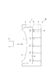
- FIG. 2 is a cross-sectional view of the optical device.
- the optical device 10 includes a mirror 1, a base plate 5, and a plurality of shape error correction units (correction units) 2.
- the mirror 1 is an optical element having a reflective surface 1 a that reflects light and a back surface 1 b that is the surface opposite to the reflective surface.
- the mirror 1 is fixed to the base plate 5 via a fixing member 6.
- the base plate 5 is spaced apart on the back surface 1b.
- the correction unit 2 is disposed between the mirror 1 and the base plate 5, and the first permanent magnet (mirror side magnet) 3 on the mirror side disposed on the back surface 1 b of the mirror 1 and the base side disposed on the opposing base plate 5
- the correction unit 2 can generate a suction force or a repulsive force by inverting and installing the polarity of the base-side magnet 4 facing the mirror-side magnet 3. Further, by adjusting the inter-magnet distance between the mirror-side magnet 3 and the base-side magnet 4 facing the mirror-side magnet 3 using the adjustment mechanism 13, the amount of generated force can be adjusted.
- the distance between the magnets is adjusted by adjusting the position where the base-side magnet 4 is disposed by the adjustment mechanism 13.
- the present invention is not limited to this, and the attraction force and the repulsive force may be switched by changing the polarity of the mirror-side magnet 3.
- the shape of the reflective surface 1a of the mirror 1 is measured using the measurement unit 12, and the direction and amount of force (shape error) required to correct the error of the shape are calculated.
- the measurement unit 12 is configured of a measurement instrument that measures the shape of the reflection surface 1 a of the mirror 1, such as a laser interferometer or a Shack-Hartmann sensor.
- the polarity of the base-side magnet 4 of each correction unit 2 is selected according to the positive / negative (concave / convex) of the shape error indicating the direction and amount of force required to correct the error of the shape, and either attraction or repulsion
- the distance between the mirror side magnet 3 and the base side magnet 4 of each correction unit 2 is adjusted by the adjustment mechanism 13 to adjust the generated force.
- the plurality of correction units 2 partially generate tensile stress or compressive stress on the mirror 1. Therefore, the mirror surface 1a is partially elastically deformed according to the tensile stress or the compressive stress, and the shape error of the mirror surface 1a is corrected.
- the shape error of the mirror 1 can be corrected without the heat generated by the shape correction mechanism due to the correction unit 2 configured by the permanent magnet.
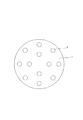
- FIG. 3 is a front view looking at the optical device 10 in the direction of arrow A in FIG.
- the correction units 2 are disposed at four locations at 90 ° intervals on the same circumference, and at eight locations at 45 ° intervals on another further outer circumference.
- the arrangement of the correction unit 2 is not limited to this, and the number and arrangement may be changed according to the optical aberration to be corrected.
- the optical device of this embodiment can be variously modified without departing from the scope of the invention.
- the number, arrangement, and the like of the correction units 2 can be set arbitrarily.
- the outer peripheral portion of the mirror 1 is fixed to the base plate 5 by the fixing member 6, any part of the mirror 1 may be fixed to the base plate 5 by the fixing member 6.
- means such as screws or adhesion may be adopted for connecting the mirror 1 and the base plate 5.
- a spherical mirror having a circular concave surface is used as the mirror 1
- the present invention is not limited thereto.
- a flat mirror or a spherical mirror having a convex surface may be used as the mirror 1.
- the measuring unit 12 has been described by way of example of a sensor that measures the surface shape, but a sensor array configured of a plurality of displacement sensors that measure a plurality of positions of the mirror 1 may be used.
- FIG. 4 is a cross-sectional view of the optical device according to the second embodiment.
- the optical device 20 is, for example, a large-diameter concave mirror device used for a reflection mirror type exposure device, and can be applied to the mirror 1 in the exposure device of FIG.
- the optical device 20 corrects, for example, the optical aberration of the projection optical system, the magnification and distortion of the projection image, and the focus by deforming the reflection surface 1a of the mirror 1 included in the projection optical system of the exposure apparatus.
- the optical device 20 includes a mirror 1, a base plate 5, a plurality of actuators 7, a plurality of displacement sensors 14, and a control unit 11.
- the control unit 11 includes a CPU, a memory, and the like, and controls the displacement sensor 14 and the plurality of actuators 7.
- the actuator 7 is disposed between the mirror 1 and the base plate 5 and applies a force to the back surface 1 b of the mirror 1.
- the actuator 7 has a mover magnet 8 fixed to the back surface 1 b and a stator coil 9 fixed to the base plate 5.
- the displacement sensor 14 measures the distance to the back surface 1 b of the mirror 1. Based on the measurement value of the displacement sensor 14, the control command value of the actuator 7 is calculated by the control unit 11, and a desired force is generated. Thereby, the reflection surface 1a of the mirror 1 can be deformed at high speed and with high accuracy, and optical aberration in the projection optical system UM can be corrected in real time and with high accuracy.
- the optical device 20 also has a correction unit 2.
- the correction unit 2 is arranged between the mirror 1 and the base plate 5 and is composed of the mirror side magnet 3 disposed on the back surface 1 b of the mirror 1 and the base side magnet 4 disposed on the base plate 5 facing the mirror 1.
- the shape correction method by the correction unit 2 is the same as that of the first embodiment.
- the measurement unit 12 may be used as in the first embodiment, or the displacement sensor 14 may be used.
- the processing accuracy required for the mirror 1 is high, but the processing error can be corrected by the correction unit 2 Therefore, processing time and processing cost of the mirror 1 can be suppressed.
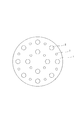
- FIG. 5 is a front view looking at the optical device 20 in the direction of arrow B in FIG.
- the correction unit 2 and the actuator 7 are respectively arranged at four locations at 90 ° intervals on the same circumference, and another 8 locations at 45 ° intervals on another outer circumference. ing.
- the arrangement of the arrangement of the correction unit 2 and the actuator 7 is not limited to this, and the number and arrangement may be changed according to the optical aberration to be corrected.
- the central portion of the mirror 1 is fixed to the base plate 5 by the fixing member 6, but any portion of the mirror 1 may be fixed to the base plate 5 by the fixing member 6.
- a non-contact type actuator such as a voice coil motor (VCM) including the mover magnet 8 and the stator coil 9 not in contact with each other, or a displacement actuator such as a piezoelectric element may be used.
- VCM voice coil motor
- a displacement actuator such as a piezoelectric element
- the optical device As described above, by performing the shape correction of the optical device with the correction unit configured by the permanent magnet, without generating heat accompanying the shape correction as shown in the first embodiment, or the second embodiment As shown in the above, it is possible to suppress heat generation and perform shape correction with high accuracy.
- an apparatus to which the optical device according to the above embodiment can be applied forms, for example, a latent image pattern of resist on a substrate by irradiation with EUV light.
- lithographic apparatus There is a lithographic apparatus.
- the present invention is applicable to a laser processing apparatus, a fundus imaging apparatus, a telescope, and the like.
- the method of manufacturing an article according to the present embodiment is suitable, for example, for manufacturing an article such as a microdevice such as a semiconductor device or an element having a microstructure.
- a latent image pattern is formed in the step of forming a latent image pattern on the photosensitive agent applied to the substrate using the above-described exposure apparatus (the step of exposing the substrate) And developing the substrate.
- a manufacturing method includes other known steps (oxidation, film formation, deposition, doping, planarization, etching, resist stripping, dicing, bonding, packaging, etc.).
- the method of manufacturing an article according to the present embodiment is advantageous in at least one of the performance, quality, productivity, and production cost of an article, as compared to the conventional method.
Abstract
Provided is an optical device capable of highly accurately correcting a shape by suppressing heat generated with shape correction of an optical element. An optical device (10) that deforms a reflecting surface (1a) of a mirror (1) has: a base plate (5) that is disposed by being separated from a rear surface (1b), i.e., the surface on the reverse side of the reflecting surface (1a); and a correction unit (2), which includes a mirror-side magnet (3) attached to the surface on the reverse side of the reflecting surface (1a), and a base-side magnet (4) that is disposed at a position in the base plate (5), said position facing the mirror-side magnet (3). The correction unit (2) corrects the shape of the reflecting surface (1a) by means of a repelling force or an attracting force generated by the mirror-side magnet (3) and the base-side magnet (4).
Description
本発明は、光学装置、露光装置及び物品の製造方法に関する。
The present invention relates to an optical apparatus, an exposure apparatus, and a method of manufacturing an article.
半導体デバイスなどの製造に用いられる露光装置の解像度を向上させるため、露光装置における投影光学系の光学収差、像倍率、像歪み、フォーカスなどの種々の光学特性を補正することが求められている。光学特性の補正は、投影光学系に含まれるミラーの形状を基準形状から変形させることで実現される。ここで、加工誤差等によりミラーの形状が基準形状からずれて形状誤差を有する場合、光学特性の補正のためには、形状誤差も考慮してミラーを変形させる必要がある。特許文献1は、ミラー取り付け時のねじ締結によって発生する理想形状(基準形状)からの形状誤差を、電磁石アクチュエータを駆動することで補正する技術を開示している。
In order to improve the resolution of an exposure apparatus used for manufacturing a semiconductor device or the like, it is required to correct various optical characteristics such as optical aberration, image magnification, image distortion, and focus of a projection optical system in the exposure apparatus. The correction of the optical characteristics is realized by deforming the shape of the mirror included in the projection optical system from the reference shape. Here, if the shape of the mirror deviates from the reference shape due to a processing error or the like and has a shape error, it is necessary to deform the mirror in consideration of the shape error in order to correct the optical characteristics. Patent Document 1 discloses a technique of correcting a shape error from an ideal shape (reference shape) generated by screw fastening at the time of mirror attachment by driving an electromagnet actuator.
しかしながら、上記文献の技術を用いて、電磁石アクチュエータにより形状誤差を補正しつつ、光学特性の補正のためにミラーを変形させる場合、電磁石アクチュエータからの発熱によりミラーに意図しない変形が起こり、新たな光学収差が生じうる。
However, in the case where the mirror is deformed to correct the optical characteristics while correcting the shape error by the electromagnet actuator using the technique of the above-mentioned document, the heat generated from the electromagnet actuator causes unintended deformation of the mirror and new optical Aberrations can occur.
本発明は、例えば、光学素子の形状補正に伴う発熱を抑制し、高精度に形状を補正することが可能な光学装置を提供することを目的とする。
An object of the present invention is, for example, to provide an optical device capable of correcting the shape with high accuracy by suppressing heat generation accompanying the shape correction of the optical element.
上記課題を解決するために、本発明の一側面である光学装置は、光学素子の反射面を変形させる光学装置であって、前記反射面の反対側の面に離間して配置されるベースプレートと、前記反射面の反対側の面に取り付けられる第1の永久磁石と、前記ベースプレートの前記第1の永久磁石に対向する位置に配置される第2の永久磁石とを含む補正ユニットと、を有し、前記補正ユニットは、前記第1の永久磁石と前記第2の永久磁石により発生する反発力または吸引力により、前記反射面の形状を補正する。
In order to solve the above problems, an optical device according to one aspect of the present invention is an optical device that deforms a reflective surface of an optical element, and a base plate disposed apart from the surface on the opposite side of the reflective surface A correction unit including: a first permanent magnet attached to the surface opposite to the reflecting surface; and a second permanent magnet disposed at a position facing the first permanent magnet of the base plate The correction unit corrects the shape of the reflecting surface by a repulsive force or an attractive force generated by the first permanent magnet and the second permanent magnet.
本発明によれば、例えば、光学素子の形状補正に伴う発熱を抑制し、高精度に形状を補正することが可能な光学装置を提供することができる。
According to the present invention, for example, it is possible to provide an optical device capable of correcting the shape with high accuracy by suppressing the heat generation accompanying the shape correction of the optical element.
図1は、露光装置の概略構成を示す図である。露光装置50は、照明光学系ILと、投影光学系UMと、マスク55を保持して移動可能なマスクステージMSと、基板56を保持して移動可能な基板ステージPSとを含む。また、露光装置50は、基板56を露光する処理を制御する制御部51を含む。
FIG. 1 is a view showing a schematic configuration of an exposure apparatus. The exposure apparatus 50 includes an illumination optical system IL, a projection optical system UM, a mask stage MS which can move while holding the mask 55, and a substrate stage PS which can move while holding the substrate 56. The exposure apparatus 50 also includes a control unit 51 that controls the process of exposing the substrate 56.
照明光学系ILに含まれる光源(不図示)から射出された光は、照明光学系ILに含まれるスリット(不図示)によって、例えば、Y方向に長い円弧状の照明領域をマスク55上に形成することができる。マスク55および基板56は、マスクステージMSおよび基板ステージPSによってそれぞれ保持されており、投影光学系UMを介して光学的にほぼ共役な位置(投影光学系UMの物体面および像面の位置)に配置される。投影光学系UMは、所定の投影倍率(例えば1/2倍)を有し、マスク55に形成されたパターンを基板56に投影する。そして、マスクステージMSおよび基板ステージPSを、投影光学系UMの物体面と平行な方向(例えば図1のX方向)に、投影光学系UMの投影倍率に応じた速度比で走査させる。これにより、マスク55に形成されたパターンを基板56に転写することができる。
The light emitted from the light source (not shown) included in the illumination optical system IL forms, for example, an arc-shaped illumination area long in the Y direction on the mask 55 by a slit (not shown) included in the illumination optical system IL. can do. The mask 55 and the substrate 56 are held by the mask stage MS and the substrate stage PS, respectively, and are at a substantially optically conjugate position (the position of the object plane and the image plane of the projection optical system UM) via the projection optical system UM. Be placed. The projection optical system UM has a predetermined projection magnification (for example, 1⁄2), and projects the pattern formed on the mask 55 onto the substrate 56. Then, the mask stage MS and the substrate stage PS are scanned in a direction parallel to the object surface of the projection optical system UM (for example, the X direction in FIG. 1) at a speed ratio corresponding to the projection magnification of the projection optical system UM. Thereby, the pattern formed on the mask 55 can be transferred to the substrate 56.
投影光学系UMは、例えば、図1に示すように、平面鏡52と、凹面鏡であるミラー1と、凸面鏡54とを含むように構成される。照明光学系ILから出射し、マスク55を透過した露光光は、平面鏡52の第1面52aにより光路を折り曲げられ、ミラー1の第1面1a1に入射する。ミラー1の第1面1a1において反射した露光光は、凸面鏡54において反射し、ミラー1の第2面1a2に入射する。ミラー1の第2面1a2において反射した露光光は、平面鏡52の第2面52bにより光路を折り曲げられ、基板56上に結像する。
The projection optical system UM is configured to include, for example, a plane mirror 52, a mirror 1 which is a concave mirror, and a convex mirror 54, as shown in FIG. The exposure light emitted from the illumination optical system IL and transmitted through the mask 55 has its optical path bent by the first surface 52 a of the plane mirror 52 and enters the first surface 1 a 1 of the mirror 1. The exposure light reflected on the first surface 1 a 1 of the mirror 1 is reflected on the convex mirror 54 and is incident on the second surface 1 a 2 of the mirror 1. The exposure light reflected by the second surface 1 a 2 of the mirror 1 is bent along the optical path by the second surface 52 b of the plane mirror 52 and forms an image on the substrate 56.
次に、図2および図3を参照して第1実施形態の光学装置10および形状誤差の補正方法について説明する。光学装置10は、例えば、反射ミラー型の露光装置に用いられる大口径凹面ミラー装置である。図2は、光学装置の断面図である。光学装置10は、ミラー1とベースプレート5と複数の形状誤差補正ユニット(補正ユニット)2とを備える。ミラー1は、光を反射する反射面1aと、反射面の反対側の面である裏面1bとを有する光学素子である。ミラー1は、固定部材6を介して、ベースプレート5に固定されている。ベースプレート5は、裏面1bに離間して配置されている。
Next, the optical device 10 according to the first embodiment and the method of correcting the shape error will be described with reference to FIGS. 2 and 3. The optical device 10 is, for example, a large aperture concave mirror device used in a reflection mirror type exposure device. FIG. 2 is a cross-sectional view of the optical device. The optical device 10 includes a mirror 1, a base plate 5, and a plurality of shape error correction units (correction units) 2. The mirror 1 is an optical element having a reflective surface 1 a that reflects light and a back surface 1 b that is the surface opposite to the reflective surface. The mirror 1 is fixed to the base plate 5 via a fixing member 6. The base plate 5 is spaced apart on the back surface 1b.
補正ユニット2はミラー1とベースプレート5の間に配置され、ミラー1の裏面1bに設置されたミラー側の第1の永久磁石(ミラー側磁石)3と、対向するベースプレート5に配置されたベース側の第2の永久磁石(ベース側磁石)4とで構成されている。補正ユニット2は、ミラー側磁石3に対向するベース側磁石4の極性を反転させて設置することで、吸引力または反発力を発生することができる。また、ミラー側磁石3と対向するベース側磁石4との磁石間距離を、調整機構13を用いて調整することで、発生する力の量を調整することができる。具体的には、調整機構13によりベース側磁石4の配置する位置を調整することで、磁石間距離を調整する。なお、本実施形態においてはベース側磁石4の極性を変える場合を説明したが、これに限られるものではなく、ミラー側磁石3の極性を変えることで吸引力と反発力を切り替えてもよい。
The correction unit 2 is disposed between the mirror 1 and the base plate 5, and the first permanent magnet (mirror side magnet) 3 on the mirror side disposed on the back surface 1 b of the mirror 1 and the base side disposed on the opposing base plate 5 The second permanent magnet (base-side magnet) 4 of FIG. The correction unit 2 can generate a suction force or a repulsive force by inverting and installing the polarity of the base-side magnet 4 facing the mirror-side magnet 3. Further, by adjusting the inter-magnet distance between the mirror-side magnet 3 and the base-side magnet 4 facing the mirror-side magnet 3 using the adjustment mechanism 13, the amount of generated force can be adjusted. Specifically, the distance between the magnets is adjusted by adjusting the position where the base-side magnet 4 is disposed by the adjustment mechanism 13. Although the case of changing the polarity of the base-side magnet 4 has been described in the present embodiment, the present invention is not limited to this, and the attraction force and the repulsive force may be switched by changing the polarity of the mirror-side magnet 3.
次に、補正ユニット2を用いたミラー1の形状誤差補正方法について説明する。計測部12を用いてミラー1の反射面1aの形状を測定し、形状の誤差を補正するために必要な力の方向および量(形状誤差)を算出する。計測部12は、レーザ干渉計やシャック・ハルトマンセンサなど、ミラー1の反射面1aの形状を計測する計測器で構成される。
Next, a method of correcting the shape error of the mirror 1 using the correction unit 2 will be described. The shape of the reflective surface 1a of the mirror 1 is measured using the measurement unit 12, and the direction and amount of force (shape error) required to correct the error of the shape are calculated. The measurement unit 12 is configured of a measurement instrument that measures the shape of the reflection surface 1 a of the mirror 1, such as a laser interferometer or a Shack-Hartmann sensor.
形状の誤差を補正するために必要な力の方向および量を示す形状誤差の正負(凹凸)に応じて、各補正ユニット2のベース側磁石4の極性を選択し、吸引力または反発力のいずれかを発生させる。形状誤差の大きさに応じて、各補正ユニット2のミラー側磁石3とベース側磁石4の磁石間距離を調整機構13により調節して、発生力を調整する。複数の補正ユニット2によって、ミラー1に部分的に引張応力或いは圧縮応力が生じる。そのため、ミラー面1aが引張応力あるいは圧縮応力に応じて部分的に弾性変形し、ミラー面1aの形状誤差が補正される。本実施形態の光学装置10は、永久磁石で構成される補正ユニット2により形状補正機構が発熱することなくミラー1の形状誤差を補正することができる。
The polarity of the base-side magnet 4 of each correction unit 2 is selected according to the positive / negative (concave / convex) of the shape error indicating the direction and amount of force required to correct the error of the shape, and either attraction or repulsion To generate According to the size of the shape error, the distance between the mirror side magnet 3 and the base side magnet 4 of each correction unit 2 is adjusted by the adjustment mechanism 13 to adjust the generated force. The plurality of correction units 2 partially generate tensile stress or compressive stress on the mirror 1. Therefore, the mirror surface 1a is partially elastically deformed according to the tensile stress or the compressive stress, and the shape error of the mirror surface 1a is corrected. In the optical device 10 according to the present embodiment, the shape error of the mirror 1 can be corrected without the heat generated by the shape correction mechanism due to the correction unit 2 configured by the permanent magnet.
次に、図3を参照して補正ユニット2の配置について説明する。図3は、図2の矢印Aの方向で光学装置10を見た正面図である。補正ユニット2は、同一円周上に90°間隔で4箇所に配置し、それとは別のさらに外側の円周上に45°間隔でさらに8箇所に配置する。しかしながら、補正ユニット2の配置はこれに限られるものではなく、補正したい光学収差によって個数および配置を変えてもよい。
Next, the arrangement of the correction unit 2 will be described with reference to FIG. FIG. 3 is a front view looking at the optical device 10 in the direction of arrow A in FIG. The correction units 2 are disposed at four locations at 90 ° intervals on the same circumference, and at eight locations at 45 ° intervals on another further outer circumference. However, the arrangement of the correction unit 2 is not limited to this, and the number and arrangement may be changed according to the optical aberration to be corrected.
なお、本実施形態の光学装置は要旨を逸脱しない範囲で種々に変形することが可能である。例えば、補正ユニット2の数や配置等を任意に設定することが可能である。また、ミラー1の外周部を固定部材6によってベースプレート5に固定しているが、ミラー1の任意の箇所を固定部材6によってベースプレート5に固定してもよい。また、ミラー1とベースプレート5の連結に、ねじや接着等の手段を採用してもよい。第1実施形態では、円形の凹面を有する球面ミラーをミラー1として用いる例について説明したが、それに限られるものではなく、例えば、平面ミラーや凸面を有する球面ミラーをミラー1として用いてもよい。計測部12は、面形状を計測するセンサを例に説明したが、ミラー1の複数の位置を計測する複数の変位センサで構成されたセンサアレイを用いてもよい。
The optical device of this embodiment can be variously modified without departing from the scope of the invention. For example, the number, arrangement, and the like of the correction units 2 can be set arbitrarily. Further, although the outer peripheral portion of the mirror 1 is fixed to the base plate 5 by the fixing member 6, any part of the mirror 1 may be fixed to the base plate 5 by the fixing member 6. Further, means such as screws or adhesion may be adopted for connecting the mirror 1 and the base plate 5. In the first embodiment, an example in which a spherical mirror having a circular concave surface is used as the mirror 1 has been described. However, the present invention is not limited thereto. For example, a flat mirror or a spherical mirror having a convex surface may be used as the mirror 1. The measuring unit 12 has been described by way of example of a sensor that measures the surface shape, but a sensor array configured of a plurality of displacement sensors that measure a plurality of positions of the mirror 1 may be used.
次に、図4および図5を参照して第2実施形態の光学装置20および形状誤差の補正方法について説明する。なお、図4および図5において、第1実施形態と共通する部材には同じ符号を付し、その説明を省略する。図4は、第2実施形態に係る光学装置の断面図である。光学装置20は、例えば、反射ミラー型の露光装置に用いられる大口径凹面ミラー装置であり、図1の露光装置ではミラー1に適用されうる。第2実施形態の光学装置20は、例えば、露光装置の投影光学系に含まれるミラー1の反射面1aを変形させることによって投影光学系の光学収差や、投影像の倍率や歪みやフォーカスを補正する。光学装置20は、ミラー1と、ベースプレート5と、複数のアクチュエータ7と、複数の変位センサ14と、制御部11とを含む。
Next, an optical device 20 according to a second embodiment and a method of correcting a shape error will be described with reference to FIGS. 4 and 5. In FIG. 4 and FIG. 5, the members common to the first embodiment are given the same reference numerals, and the description thereof will be omitted. FIG. 4 is a cross-sectional view of the optical device according to the second embodiment. The optical device 20 is, for example, a large-diameter concave mirror device used for a reflection mirror type exposure device, and can be applied to the mirror 1 in the exposure device of FIG. The optical device 20 according to the second embodiment corrects, for example, the optical aberration of the projection optical system, the magnification and distortion of the projection image, and the focus by deforming the reflection surface 1a of the mirror 1 included in the projection optical system of the exposure apparatus. Do. The optical device 20 includes a mirror 1, a base plate 5, a plurality of actuators 7, a plurality of displacement sensors 14, and a control unit 11.
制御部11は、CPUやメモリなどを有し、変位センサ14と複数のアクチュエータ7を制御する。アクチュエータ7は、ミラー1とベースプレート5との間に配置され、ミラー1の裏面1bに力を加える。アクチュエータ7は、裏面1bに固定された可動子磁石8とベースプレート5に固定されている固定子コイル9を有する。変位センサ14は、ミラー1の裏面1bまでの距離を計測する。変位センサ14の計測値をもとに制御部11でアクチュエータ7の駆動指令値が算出され、所望の力が発生される。これにより、ミラー1の反射面1aを高速かつ高精度に変形させることができ、投影光学系UMにおける光学収差をリアルタイムかつ高精度に補正することができる。
The control unit 11 includes a CPU, a memory, and the like, and controls the displacement sensor 14 and the plurality of actuators 7. The actuator 7 is disposed between the mirror 1 and the base plate 5 and applies a force to the back surface 1 b of the mirror 1. The actuator 7 has a mover magnet 8 fixed to the back surface 1 b and a stator coil 9 fixed to the base plate 5. The displacement sensor 14 measures the distance to the back surface 1 b of the mirror 1. Based on the measurement value of the displacement sensor 14, the control command value of the actuator 7 is calculated by the control unit 11, and a desired force is generated. Thereby, the reflection surface 1a of the mirror 1 can be deformed at high speed and with high accuracy, and optical aberration in the projection optical system UM can be corrected in real time and with high accuracy.
また、光学装置20は、補正ユニット2を有している。補正ユニット2は、ミラー1とベースプレート5の間に配置され、ミラー1の裏面1bに設置されたミラー側磁石3と対向するベースプレート5に配置されたベース側磁石4とで構成されている。補正ユニット2による形状補正方法は、第1実施形態と同様である。形状誤差の測定には、第1実施形態と同様に計測部12を用いてもよいし、変位センサ14を用いてもよい。
The optical device 20 also has a correction unit 2. The correction unit 2 is arranged between the mirror 1 and the base plate 5 and is composed of the mirror side magnet 3 disposed on the back surface 1 b of the mirror 1 and the base side magnet 4 disposed on the base plate 5 facing the mirror 1. The shape correction method by the correction unit 2 is the same as that of the first embodiment. For the measurement of the shape error, the measurement unit 12 may be used as in the first embodiment, or the displacement sensor 14 may be used.
ミラー1の組立誤差や加工誤差に起因する形状誤差を、この各アクチュエータ7で補正を行うと、形状誤差に応じて必要な力を常時出し続けなければならないので発熱が大きくなってしまい、ミラー1に意図しない変形をもたらしてしまう。しかし、補正ユニット2を用いて組立誤差や加工誤差に起因する形状誤差を補正することで、発熱することなく組立誤差や加工誤差に起因する形状誤差を補正することができる。これにより各アクチュエータは、投影光学系UMにおける光学収差の補正に必要な変形駆動量に対して必要な力のみを発生すればよくなるので、相対的に発熱を抑えることができる。さらに、一般的に第2実施形態のように複数のアクチュエータで変形駆動を行う光学装置20においてはミラー1に要求される加工精度は高くなるが、加工誤差を補正ユニット2で補正することができるので、ミラー1の加工時間および加工コストを抑制できる。
If a shape error due to an assembly error or a processing error of the mirror 1 is corrected by each of the actuators 7, it is necessary to continuously continuously provide a necessary force according to the shape error, so the heat generation becomes large. Brings unintended deformations to However, by correcting the shape error due to the assembly error or the processing error using the correction unit 2, it is possible to correct the shape error due to the assembly error or the processing error without generating heat. As a result, since each actuator only needs to generate a force necessary for the deformation drive amount required to correct the optical aberration in the projection optical system UM, heat generation can be relatively suppressed. Furthermore, in the optical device 20 that generally performs deformation drive with a plurality of actuators as in the second embodiment, the processing accuracy required for the mirror 1 is high, but the processing error can be corrected by the correction unit 2 Therefore, processing time and processing cost of the mirror 1 can be suppressed.
次に、図5を用いて補正ユニット2およびアクチュエータ7の配置について説明する。図5は、図4の矢印Bの方向で光学装置20を見た正面図である。第2実施形態では、補正ユニット2およびアクチュエータ7をそれぞれ同一円周上に90°間隔で4箇所ずつ配置し、それとは別のさらに外側の円周上に45°間隔でさらに8箇所ずつ配置している。しかしながら、補正ユニット2およびアクチュエータ7の配置の配置はこれに限られるものではなく、補正したい光学収差によって個数および配置を変えてもよい。
Next, the arrangement of the correction unit 2 and the actuator 7 will be described with reference to FIG. FIG. 5 is a front view looking at the optical device 20 in the direction of arrow B in FIG. In the second embodiment, the correction unit 2 and the actuator 7 are respectively arranged at four locations at 90 ° intervals on the same circumference, and another 8 locations at 45 ° intervals on another outer circumference. ing. However, the arrangement of the arrangement of the correction unit 2 and the actuator 7 is not limited to this, and the number and arrangement may be changed according to the optical aberration to be corrected.
第2実施形態では、ミラー1の中心部を固定部材6によってベースプレート5に固定しているが、ミラー1の任意の箇所を固定部材6によってベースプレート5に固定してもよい。各アクチュエータ7としては、例えば、ボイスコイルモータ(VCM)など、互いに接触しない可動子磁石8と固定子コイル9とを含む非接触型のアクチュエータや、圧電素子などの変位アクチュエータが用いられてもよい。
In the second embodiment, the central portion of the mirror 1 is fixed to the base plate 5 by the fixing member 6, but any portion of the mirror 1 may be fixed to the base plate 5 by the fixing member 6. As each actuator 7, for example, a non-contact type actuator such as a voice coil motor (VCM) including the mover magnet 8 and the stator coil 9 not in contact with each other, or a displacement actuator such as a piezoelectric element may be used. .
以上説明したように、永久磁石で構成された補正ユニットで光学装置の形状補正を行うことで、第1実施形態に示したように形状補正に伴う発熱をすることなく、または、第2実施形態に示したように発熱を抑制して、高精度な形状補正を行うことができる。なお、上記実施形態では、露光装置に適用する例を説明したが、上記実施形態に係る光学装置を適用可能な装置は、例えば、EUV光の照射により基板上にレジストの潜像パターンを形成するリソグラフィ装置がある。その他、レーザ加工装置、眼底撮影装置、望遠鏡等にも適用可能である。
As described above, by performing the shape correction of the optical device with the correction unit configured by the permanent magnet, without generating heat accompanying the shape correction as shown in the first embodiment, or the second embodiment As shown in the above, it is possible to suppress heat generation and perform shape correction with high accuracy. In the above embodiment, an example of application to an exposure apparatus has been described, but an apparatus to which the optical device according to the above embodiment can be applied forms, for example, a latent image pattern of resist on a substrate by irradiation with EUV light. There is a lithographic apparatus. In addition, the present invention is applicable to a laser processing apparatus, a fundus imaging apparatus, a telescope, and the like.
本実施形態にかかる物品の製造方法は、例えば、半導体デバイス等のマイクロデバイスや微細構造を有する素子等の物品を製造するのに好適である。本実施形態の物品の製造方法は、基板に塗布された感光剤に上記の露光装置を用いて潜像パターンを形成する工程(基板を露光する工程)と、かかる工程で潜像パターンが形成された基板を現像する工程とを含む。さらに、かかる製造方法は、他の周知の工程(酸化、成膜、蒸着、ドーピング、平坦化、エッチング、レジスト剥離、ダイシング、ボンディング、パッケージング等)を含む。本実施形態の物品の製造方法は、従来の方法に比べて、物品の性能・品質・生産性・生産コストの少なくとも1つにおいて有利である。
The method of manufacturing an article according to the present embodiment is suitable, for example, for manufacturing an article such as a microdevice such as a semiconductor device or an element having a microstructure. In the method of manufacturing an article according to the present embodiment, a latent image pattern is formed in the step of forming a latent image pattern on the photosensitive agent applied to the substrate using the above-described exposure apparatus (the step of exposing the substrate) And developing the substrate. Furthermore, such a manufacturing method includes other known steps (oxidation, film formation, deposition, doping, planarization, etching, resist stripping, dicing, bonding, packaging, etc.). The method of manufacturing an article according to the present embodiment is advantageous in at least one of the performance, quality, productivity, and production cost of an article, as compared to the conventional method.
以上、本発明の好ましい実施形態について説明したが、本発明は、これらの実施形態に限定されず、その要旨の範囲内で種々の変形および変更が可能である。
Although the preferred embodiments of the present invention have been described above, the present invention is not limited to these embodiments, and various modifications and changes are possible within the scope of the present invention.
1 ミラー
2 補正ユニット
3 ミラー側磁石
4 ベース側磁石
5 ベースプレート 1mirror 2 correction unit 3 mirror side magnet 4 base side magnet 5 base plate
2 補正ユニット
3 ミラー側磁石
4 ベース側磁石
5 ベースプレート 1
Claims (10)
- 光学素子の反射面を変形させる光学装置であって、
前記反射面の反対側の面に離間して配置されるベースプレートと、
前記反射面の反対側の面に取り付けられる第1の永久磁石と、前記ベースプレートの前記第1の永久磁石に対向する位置に配置される第2の永久磁石とを含む補正ユニットと、を有し、
前記補正ユニットは、前記第1の永久磁石と前記第2の永久磁石により発生する反発力または吸引力により、前記反射面の形状を補正することを特徴とする光学装置。 An optical device for deforming a reflection surface of an optical element, comprising:
A base plate spaced apart on a surface opposite to the reflective surface;
The correction unit includes: a first permanent magnet attached to the surface opposite to the reflecting surface; and a second permanent magnet disposed at a position facing the first permanent magnet of the base plate ,
The optical device according to claim 1, wherein the correction unit corrects the shape of the reflection surface by a repulsive force or a suction force generated by the first permanent magnet and the second permanent magnet. - 前記第2の永久磁石の極性を変えることで、前記反発力と前記吸引力を切り替えることを特徴とする請求項1に記載の光学装置。 The optical device according to claim 1, wherein the repulsive force and the attractive force are switched by changing the polarity of the second permanent magnet.
- 前記第2の永久磁石の極性は、前記反射面の形状を測定する計測部により計測された形状誤差に基づいて変えることを特徴とする請求項2に記載の光学装置。 The optical device according to claim 2, wherein the polarity of the second permanent magnet is changed based on a shape error measured by a measurement unit that measures the shape of the reflection surface.
- 前記第2の永久磁石の位置を調整することで、前記第1の永久磁石と前記第2の永久磁石との距離を調整する調整機構をさらに有することを特徴とする請求項1ないし3のうちいずれか1項に記載の光学装置。 4. The apparatus according to claim 1, further comprising an adjusting mechanism for adjusting a distance between the first permanent magnet and the second permanent magnet by adjusting a position of the second permanent magnet. The optical device according to any one of the items.
- 前記調整機構は、前記反射面の形状を測定する計測部により計測された形状誤差に基づいて前記第2の永久磁石の位置を調整することを特徴とする請求項4に記載の光学装置。 5. The optical device according to claim 4, wherein the adjustment mechanism adjusts the position of the second permanent magnet based on a shape error measured by a measurement unit that measures the shape of the reflection surface.
- 前記反射面の反対側の面に取り付けられた磁石と、前記ベースプレートの前記磁石に対向する位置に配置されるコイルとを含むアクチュエータをさらに有することを特徴とする請求項1ないし5のうちいずれか1項に記載の光学装置。 The actuator according to any one of claims 1 to 5, further comprising an actuator including a magnet attached to a surface opposite to the reflecting surface, and a coil disposed at a position facing the magnet on the base plate. An optical device according to item 1.
- 前記ベースプレートに配置された、前記ベースプレートと前記反射面の反対側の面との距離を計測する変位センサをさらに有することを特徴とする請求項6に記載の光学装置。 The optical device according to claim 6, further comprising a displacement sensor disposed on the base plate and measuring a distance between the base plate and a surface opposite to the reflection surface.
- 前記アクチュエータは、前記変位センサが計測した前記距離に基づいて駆動することを特徴とする請求項7に記載の光学装置。 The optical device according to claim 7, wherein the actuator is driven based on the distance measured by the displacement sensor.
- 請求項1ないし8のいずれか1項に記載の光学装置を有することを特徴とする露光装置。 An exposure apparatus comprising the optical device according to any one of claims 1 to 8.
- 請求項9に記載の露光装置を用いて基板を露光する工程と、
前記露光された前記基板を現像する工程と、を含む
ことを特徴とする物品の製造方法。 Exposing the substrate using the exposure apparatus according to claim 9;
And b. Developing the exposed substrate.
Priority Applications (2)
| Application Number | Priority Date | Filing Date | Title |
|---|---|---|---|
| CN201780040473.6A CN109416457B (en) | 2016-07-06 | 2017-06-16 | Optical device, exposure device, and method for manufacturing article |
| KR1020197002601A KR102165797B1 (en) | 2016-07-06 | 2017-06-16 | Optical device, exposure device, and manufacturing method of article |
Applications Claiming Priority (2)
| Application Number | Priority Date | Filing Date | Title |
|---|---|---|---|
| JP2016134000A JP6929024B2 (en) | 2016-07-06 | 2016-07-06 | Manufacturing method of optical equipment, exposure equipment and articles |
| JP2016-134000 | 2016-07-06 |
Publications (1)
| Publication Number | Publication Date |
|---|---|
| WO2018008364A1 true WO2018008364A1 (en) | 2018-01-11 |
Family
ID=60912605
Family Applications (1)
| Application Number | Title | Priority Date | Filing Date |
|---|---|---|---|
| PCT/JP2017/022311 WO2018008364A1 (en) | 2016-07-06 | 2017-06-16 | Optical device, exposure device, and method for manufacturing article |
Country Status (4)
| Country | Link |
|---|---|
| JP (1) | JP6929024B2 (en) |
| KR (1) | KR102165797B1 (en) |
| CN (1) | CN109416457B (en) |
| WO (1) | WO2018008364A1 (en) |
Families Citing this family (1)
| Publication number | Priority date | Publication date | Assignee | Title |
|---|---|---|---|---|
| CN109932804B (en) * | 2019-03-04 | 2021-06-01 | 杭州电子科技大学 | Flexible memory alloy supporting device of small-caliber light reflector |
Citations (5)
| Publication number | Priority date | Publication date | Assignee | Title |
|---|---|---|---|---|
| JP2005004146A (en) * | 2002-07-03 | 2005-01-06 | Nikon Corp | Reflection optical device and exposure device |
| JP2011119551A (en) * | 2009-12-04 | 2011-06-16 | Nikon Corp | Optical member deformation apparatus, optical system, aligner, method of manufacturing device |
| JP2011530721A (en) * | 2008-08-14 | 2011-12-22 | アルパオ | Force mirror and variable mirror with distributed stiffness |
| JP2014147169A (en) * | 2013-01-28 | 2014-08-14 | Mitsubishi Electric Corp | Variable shape mirror device |
| JP2015126037A (en) * | 2013-12-25 | 2015-07-06 | キヤノン株式会社 | Optical device, projecting optical system, exposure device and manufacturing method for object |
Family Cites Families (9)
| Publication number | Priority date | Publication date | Assignee | Title |
|---|---|---|---|---|
| JPH02101402A (en) | 1988-10-11 | 1990-04-13 | Omron Tateisi Electron Co | Reflecting mirror device |
| US7589822B2 (en) | 2004-02-02 | 2009-09-15 | Nikon Corporation | Stage drive method and stage unit, exposure apparatus, and device manufacturing method |
| JP2008310925A (en) | 2007-06-18 | 2008-12-25 | Sony Corp | Deformable mirror device, optical pickup, and optical drive device |
| FR2923301B1 (en) | 2007-11-02 | 2010-09-17 | Ujf Filiale | DEFORMABLE MIRROR WITH DISTRIBUTED RAIDEUR, TOOL AND METHOD FOR REALIZING SUCH A MIRROR |
| CN103891114B (en) | 2011-10-27 | 2018-01-02 | 不列颠哥伦比亚大学 | Gearshift and its manufacture, use and control method |
| JP2015050353A (en) | 2013-09-02 | 2015-03-16 | キヤノン株式会社 | Optical device, projection optical system, exposure device, and manufacturing method of article |
| JP2015065246A (en) * | 2013-09-24 | 2015-04-09 | キヤノン株式会社 | Optical device, optical system, exposure device, and manufacturing method for article |
| JP6168957B2 (en) * | 2013-09-30 | 2017-07-26 | キヤノン株式会社 | Optical apparatus, projection optical system, exposure apparatus, and article manufacturing method |
| JP2016092366A (en) * | 2014-11-11 | 2016-05-23 | キヤノン株式会社 | Optical device, projection optical system, exposure device, and manufacturing method of article |
-
2016
- 2016-07-06 JP JP2016134000A patent/JP6929024B2/en active Active
-
2017
- 2017-06-16 WO PCT/JP2017/022311 patent/WO2018008364A1/en active Application Filing
- 2017-06-16 CN CN201780040473.6A patent/CN109416457B/en active Active
- 2017-06-16 KR KR1020197002601A patent/KR102165797B1/en active IP Right Grant
Patent Citations (5)
| Publication number | Priority date | Publication date | Assignee | Title |
|---|---|---|---|---|
| JP2005004146A (en) * | 2002-07-03 | 2005-01-06 | Nikon Corp | Reflection optical device and exposure device |
| JP2011530721A (en) * | 2008-08-14 | 2011-12-22 | アルパオ | Force mirror and variable mirror with distributed stiffness |
| JP2011119551A (en) * | 2009-12-04 | 2011-06-16 | Nikon Corp | Optical member deformation apparatus, optical system, aligner, method of manufacturing device |
| JP2014147169A (en) * | 2013-01-28 | 2014-08-14 | Mitsubishi Electric Corp | Variable shape mirror device |
| JP2015126037A (en) * | 2013-12-25 | 2015-07-06 | キヤノン株式会社 | Optical device, projecting optical system, exposure device and manufacturing method for object |
Also Published As
| Publication number | Publication date |
|---|---|
| KR102165797B1 (en) | 2020-10-14 |
| CN109416457B (en) | 2021-09-17 |
| CN109416457A (en) | 2019-03-01 |
| JP6929024B2 (en) | 2021-09-01 |
| KR20190020139A (en) | 2019-02-27 |
| JP2018005068A (en) | 2018-01-11 |
Similar Documents
| Publication | Publication Date | Title |
|---|---|---|
| JP6336274B2 (en) | Optical apparatus, projection optical system, exposure apparatus, and article manufacturing method | |
| JP6168957B2 (en) | Optical apparatus, projection optical system, exposure apparatus, and article manufacturing method | |
| US9557560B2 (en) | Mirror unit and exposure apparatus | |
| JP2008112756A (en) | Optical element driving device and control method thereof, exposure apparatus, and manufacturing method of device | |
| KR102193387B1 (en) | Holding device, projection optical system, exposure device, and article manufacturing method | |
| JP2016092309A (en) | Optical device, projection optical system, exposure device, and manufacturing method of article | |
| TWI631430B (en) | Optical device, projection optical system, exposure device, and article manufacturing method | |
| JP2009223034A (en) | Optical element holding apparatus, optical system, exposure apparatus, optical characteristic adjusting method, and method of manufacturing device | |
| WO2018008364A1 (en) | Optical device, exposure device, and method for manufacturing article | |
| US10884236B2 (en) | Optical device, projection optical system, exposure apparatus using the same, and method for manufacturing article | |
| CN108227401B (en) | Optical device, exposure device, and method for manufacturing article | |
| JP6736371B2 (en) | Position adjusting mechanism, exposure apparatus, and article manufacturing method | |
| US20230060389A1 (en) | Driving apparatus, exposure apparatus, and article manufacturing method | |
| KR102230464B1 (en) | Optical element, exposure apparatus, and article manufacturing method | |
| JP7033997B2 (en) | Exposure equipment and manufacturing method of articles | |
| JP2018066959A (en) | Optical device, projection optical system, exposure apparatus and production method of article | |
| JP6853659B2 (en) | Determining method, optical equipment, projection optical system, exposure equipment and manufacturing method of articles | |
| JP2016033999A (en) | Exposure device and goods manufacturing method |
Legal Events
| Date | Code | Title | Description |
|---|---|---|---|
| 121 | Ep: the epo has been informed by wipo that ep was designated in this application |
Ref document number: 17823971 Country of ref document: EP Kind code of ref document: A1 |
|
| NENP | Non-entry into the national phase |
Ref country code: DE |
|
| ENP | Entry into the national phase |
Ref document number: 20197002601 Country of ref document: KR Kind code of ref document: A |
|
| 122 | Ep: pct application non-entry in european phase |
Ref document number: 17823971 Country of ref document: EP Kind code of ref document: A1 |