WO2018003697A1 - Bioélectrode et procédé de production de bioélectrode - Google Patents
Bioélectrode et procédé de production de bioélectrode Download PDFInfo
- Publication number
- WO2018003697A1 WO2018003697A1 PCT/JP2017/023226 JP2017023226W WO2018003697A1 WO 2018003697 A1 WO2018003697 A1 WO 2018003697A1 JP 2017023226 W JP2017023226 W JP 2017023226W WO 2018003697 A1 WO2018003697 A1 WO 2018003697A1
- Authority
- WO
- WIPO (PCT)
- Prior art keywords
- film
- electrode film
- electrode
- silver chloride
- silver
- Prior art date
Links
Images


Classifications
-
- B—PERFORMING OPERATIONS; TRANSPORTING
- B32—LAYERED PRODUCTS
- B32B—LAYERED PRODUCTS, i.e. PRODUCTS BUILT-UP OF STRATA OF FLAT OR NON-FLAT, e.g. CELLULAR OR HONEYCOMB, FORM
- B32B3/00—Layered products comprising a layer with external or internal discontinuities or unevennesses, or a layer of non-planar form; Layered products having particular features of form
- B32B3/02—Layered products comprising a layer with external or internal discontinuities or unevennesses, or a layer of non-planar form; Layered products having particular features of form characterised by features of form at particular places, e.g. in edge regions
- B32B3/08—Layered products comprising a layer with external or internal discontinuities or unevennesses, or a layer of non-planar form; Layered products having particular features of form characterised by features of form at particular places, e.g. in edge regions characterised by added members at particular parts
-
- A—HUMAN NECESSITIES
- A61—MEDICAL OR VETERINARY SCIENCE; HYGIENE
- A61B—DIAGNOSIS; SURGERY; IDENTIFICATION
- A61B5/00—Measuring for diagnostic purposes; Identification of persons
- A61B5/24—Detecting, measuring or recording bioelectric or biomagnetic signals of the body or parts thereof
- A61B5/25—Bioelectric electrodes therefor
- A61B5/279—Bioelectric electrodes therefor specially adapted for particular uses
- A61B5/291—Bioelectric electrodes therefor specially adapted for particular uses for electroencephalography [EEG]
-
- B—PERFORMING OPERATIONS; TRANSPORTING
- B32—LAYERED PRODUCTS
- B32B—LAYERED PRODUCTS, i.e. PRODUCTS BUILT-UP OF STRATA OF FLAT OR NON-FLAT, e.g. CELLULAR OR HONEYCOMB, FORM
- B32B1/00—Layered products having a general shape other than plane
- B32B1/08—Tubular products
-
- B—PERFORMING OPERATIONS; TRANSPORTING
- B32—LAYERED PRODUCTS
- B32B—LAYERED PRODUCTS, i.e. PRODUCTS BUILT-UP OF STRATA OF FLAT OR NON-FLAT, e.g. CELLULAR OR HONEYCOMB, FORM
- B32B15/00—Layered products comprising a layer of metal
- B32B15/04—Layered products comprising a layer of metal comprising metal as the main or only constituent of a layer, which is next to another layer of the same or of a different material
- B32B15/046—Layered products comprising a layer of metal comprising metal as the main or only constituent of a layer, which is next to another layer of the same or of a different material of foam
-
- B—PERFORMING OPERATIONS; TRANSPORTING
- B32—LAYERED PRODUCTS
- B32B—LAYERED PRODUCTS, i.e. PRODUCTS BUILT-UP OF STRATA OF FLAT OR NON-FLAT, e.g. CELLULAR OR HONEYCOMB, FORM
- B32B15/00—Layered products comprising a layer of metal
- B32B15/04—Layered products comprising a layer of metal comprising metal as the main or only constituent of a layer, which is next to another layer of the same or of a different material
- B32B15/08—Layered products comprising a layer of metal comprising metal as the main or only constituent of a layer, which is next to another layer of the same or of a different material of synthetic resin
- B32B15/09—Layered products comprising a layer of metal comprising metal as the main or only constituent of a layer, which is next to another layer of the same or of a different material of synthetic resin comprising polyesters
-
- B—PERFORMING OPERATIONS; TRANSPORTING
- B32—LAYERED PRODUCTS
- B32B—LAYERED PRODUCTS, i.e. PRODUCTS BUILT-UP OF STRATA OF FLAT OR NON-FLAT, e.g. CELLULAR OR HONEYCOMB, FORM
- B32B27/00—Layered products comprising a layer of synthetic resin
- B32B27/06—Layered products comprising a layer of synthetic resin as the main or only constituent of a layer, which is next to another layer of the same or of a different material
- B32B27/065—Layered products comprising a layer of synthetic resin as the main or only constituent of a layer, which is next to another layer of the same or of a different material of foam
-
- B—PERFORMING OPERATIONS; TRANSPORTING
- B32—LAYERED PRODUCTS
- B32B—LAYERED PRODUCTS, i.e. PRODUCTS BUILT-UP OF STRATA OF FLAT OR NON-FLAT, e.g. CELLULAR OR HONEYCOMB, FORM
- B32B27/00—Layered products comprising a layer of synthetic resin
- B32B27/06—Layered products comprising a layer of synthetic resin as the main or only constituent of a layer, which is next to another layer of the same or of a different material
- B32B27/08—Layered products comprising a layer of synthetic resin as the main or only constituent of a layer, which is next to another layer of the same or of a different material of synthetic resin
-
- B—PERFORMING OPERATIONS; TRANSPORTING
- B32—LAYERED PRODUCTS
- B32B—LAYERED PRODUCTS, i.e. PRODUCTS BUILT-UP OF STRATA OF FLAT OR NON-FLAT, e.g. CELLULAR OR HONEYCOMB, FORM
- B32B27/00—Layered products comprising a layer of synthetic resin
- B32B27/12—Layered products comprising a layer of synthetic resin next to a fibrous or filamentary layer
-
- B—PERFORMING OPERATIONS; TRANSPORTING
- B32—LAYERED PRODUCTS
- B32B—LAYERED PRODUCTS, i.e. PRODUCTS BUILT-UP OF STRATA OF FLAT OR NON-FLAT, e.g. CELLULAR OR HONEYCOMB, FORM
- B32B27/00—Layered products comprising a layer of synthetic resin
- B32B27/30—Layered products comprising a layer of synthetic resin comprising vinyl (co)polymers; comprising acrylic (co)polymers
- B32B27/308—Layered products comprising a layer of synthetic resin comprising vinyl (co)polymers; comprising acrylic (co)polymers comprising acrylic (co)polymers
-
- B—PERFORMING OPERATIONS; TRANSPORTING
- B32—LAYERED PRODUCTS
- B32B—LAYERED PRODUCTS, i.e. PRODUCTS BUILT-UP OF STRATA OF FLAT OR NON-FLAT, e.g. CELLULAR OR HONEYCOMB, FORM
- B32B27/00—Layered products comprising a layer of synthetic resin
- B32B27/32—Layered products comprising a layer of synthetic resin comprising polyolefins
-
- B—PERFORMING OPERATIONS; TRANSPORTING
- B32—LAYERED PRODUCTS
- B32B—LAYERED PRODUCTS, i.e. PRODUCTS BUILT-UP OF STRATA OF FLAT OR NON-FLAT, e.g. CELLULAR OR HONEYCOMB, FORM
- B32B27/00—Layered products comprising a layer of synthetic resin
- B32B27/34—Layered products comprising a layer of synthetic resin comprising polyamides
-
- B—PERFORMING OPERATIONS; TRANSPORTING
- B32—LAYERED PRODUCTS
- B32B—LAYERED PRODUCTS, i.e. PRODUCTS BUILT-UP OF STRATA OF FLAT OR NON-FLAT, e.g. CELLULAR OR HONEYCOMB, FORM
- B32B27/00—Layered products comprising a layer of synthetic resin
- B32B27/36—Layered products comprising a layer of synthetic resin comprising polyesters
-
- B—PERFORMING OPERATIONS; TRANSPORTING
- B32—LAYERED PRODUCTS
- B32B—LAYERED PRODUCTS, i.e. PRODUCTS BUILT-UP OF STRATA OF FLAT OR NON-FLAT, e.g. CELLULAR OR HONEYCOMB, FORM
- B32B27/00—Layered products comprising a layer of synthetic resin
- B32B27/40—Layered products comprising a layer of synthetic resin comprising polyurethanes
-
- B—PERFORMING OPERATIONS; TRANSPORTING
- B32—LAYERED PRODUCTS
- B32B—LAYERED PRODUCTS, i.e. PRODUCTS BUILT-UP OF STRATA OF FLAT OR NON-FLAT, e.g. CELLULAR OR HONEYCOMB, FORM
- B32B29/00—Layered products comprising a layer of paper or cardboard
- B32B29/002—Layered products comprising a layer of paper or cardboard as the main or only constituent of a layer, which is next to another layer of the same or of a different material
- B32B29/007—Layered products comprising a layer of paper or cardboard as the main or only constituent of a layer, which is next to another layer of the same or of a different material next to a foam layer
-
- B—PERFORMING OPERATIONS; TRANSPORTING
- B32—LAYERED PRODUCTS
- B32B—LAYERED PRODUCTS, i.e. PRODUCTS BUILT-UP OF STRATA OF FLAT OR NON-FLAT, e.g. CELLULAR OR HONEYCOMB, FORM
- B32B5/00—Layered products characterised by the non- homogeneity or physical structure, i.e. comprising a fibrous, filamentary, particulate or foam layer; Layered products characterised by having a layer differing constitutionally or physically in different parts
- B32B5/02—Layered products characterised by the non- homogeneity or physical structure, i.e. comprising a fibrous, filamentary, particulate or foam layer; Layered products characterised by having a layer differing constitutionally or physically in different parts characterised by structural features of a fibrous or filamentary layer
- B32B5/022—Non-woven fabric
-
- B—PERFORMING OPERATIONS; TRANSPORTING
- B32—LAYERED PRODUCTS
- B32B—LAYERED PRODUCTS, i.e. PRODUCTS BUILT-UP OF STRATA OF FLAT OR NON-FLAT, e.g. CELLULAR OR HONEYCOMB, FORM
- B32B5/00—Layered products characterised by the non- homogeneity or physical structure, i.e. comprising a fibrous, filamentary, particulate or foam layer; Layered products characterised by having a layer differing constitutionally or physically in different parts
- B32B5/16—Layered products characterised by the non- homogeneity or physical structure, i.e. comprising a fibrous, filamentary, particulate or foam layer; Layered products characterised by having a layer differing constitutionally or physically in different parts characterised by features of a layer formed of particles, e.g. chips, powder or granules
-
- B—PERFORMING OPERATIONS; TRANSPORTING
- B32—LAYERED PRODUCTS
- B32B—LAYERED PRODUCTS, i.e. PRODUCTS BUILT-UP OF STRATA OF FLAT OR NON-FLAT, e.g. CELLULAR OR HONEYCOMB, FORM
- B32B5/00—Layered products characterised by the non- homogeneity or physical structure, i.e. comprising a fibrous, filamentary, particulate or foam layer; Layered products characterised by having a layer differing constitutionally or physically in different parts
- B32B5/18—Layered products characterised by the non- homogeneity or physical structure, i.e. comprising a fibrous, filamentary, particulate or foam layer; Layered products characterised by having a layer differing constitutionally or physically in different parts characterised by features of a layer of foamed material
-
- B—PERFORMING OPERATIONS; TRANSPORTING
- B32—LAYERED PRODUCTS
- B32B—LAYERED PRODUCTS, i.e. PRODUCTS BUILT-UP OF STRATA OF FLAT OR NON-FLAT, e.g. CELLULAR OR HONEYCOMB, FORM
- B32B7/00—Layered products characterised by the relation between layers; Layered products characterised by the relative orientation of features between layers, or by the relative values of a measurable parameter between layers, i.e. products comprising layers having different physical, chemical or physicochemical properties; Layered products characterised by the interconnection of layers
- B32B7/04—Interconnection of layers
- B32B7/06—Interconnection of layers permitting easy separation
-
- C—CHEMISTRY; METALLURGY
- C09—DYES; PAINTS; POLISHES; NATURAL RESINS; ADHESIVES; COMPOSITIONS NOT OTHERWISE PROVIDED FOR; APPLICATIONS OF MATERIALS NOT OTHERWISE PROVIDED FOR
- C09J—ADHESIVES; NON-MECHANICAL ASPECTS OF ADHESIVE PROCESSES IN GENERAL; ADHESIVE PROCESSES NOT PROVIDED FOR ELSEWHERE; USE OF MATERIALS AS ADHESIVES
- C09J9/00—Adhesives characterised by their physical nature or the effects produced, e.g. glue sticks
- C09J9/02—Electrically-conducting adhesives
-
- A—HUMAN NECESSITIES
- A61—MEDICAL OR VETERINARY SCIENCE; HYGIENE
- A61B—DIAGNOSIS; SURGERY; IDENTIFICATION
- A61B2562/00—Details of sensors; Constructional details of sensor housings or probes; Accessories for sensors
- A61B2562/02—Details of sensors specially adapted for in-vivo measurements
- A61B2562/0209—Special features of electrodes classified in A61B5/24, A61B5/25, A61B5/283, A61B5/291, A61B5/296, A61B5/053
- A61B2562/0215—Silver or silver chloride containing
-
- A—HUMAN NECESSITIES
- A61—MEDICAL OR VETERINARY SCIENCE; HYGIENE
- A61B—DIAGNOSIS; SURGERY; IDENTIFICATION
- A61B2562/00—Details of sensors; Constructional details of sensor housings or probes; Accessories for sensors
- A61B2562/12—Manufacturing methods specially adapted for producing sensors for in-vivo measurements
- A61B2562/125—Manufacturing methods specially adapted for producing sensors for in-vivo measurements characterised by the manufacture of electrodes
-
- B—PERFORMING OPERATIONS; TRANSPORTING
- B32—LAYERED PRODUCTS
- B32B—LAYERED PRODUCTS, i.e. PRODUCTS BUILT-UP OF STRATA OF FLAT OR NON-FLAT, e.g. CELLULAR OR HONEYCOMB, FORM
- B32B2250/00—Layers arrangement
- B32B2250/44—Number of layers variable across the laminate
-
- B—PERFORMING OPERATIONS; TRANSPORTING
- B32—LAYERED PRODUCTS
- B32B—LAYERED PRODUCTS, i.e. PRODUCTS BUILT-UP OF STRATA OF FLAT OR NON-FLAT, e.g. CELLULAR OR HONEYCOMB, FORM
- B32B2255/00—Coating on the layer surface
- B32B2255/10—Coating on the layer surface on synthetic resin layer or on natural or synthetic rubber layer
-
- B—PERFORMING OPERATIONS; TRANSPORTING
- B32—LAYERED PRODUCTS
- B32B—LAYERED PRODUCTS, i.e. PRODUCTS BUILT-UP OF STRATA OF FLAT OR NON-FLAT, e.g. CELLULAR OR HONEYCOMB, FORM
- B32B2255/00—Coating on the layer surface
- B32B2255/20—Inorganic coating
- B32B2255/205—Metallic coating
-
- B—PERFORMING OPERATIONS; TRANSPORTING
- B32—LAYERED PRODUCTS
- B32B—LAYERED PRODUCTS, i.e. PRODUCTS BUILT-UP OF STRATA OF FLAT OR NON-FLAT, e.g. CELLULAR OR HONEYCOMB, FORM
- B32B2255/00—Coating on the layer surface
- B32B2255/26—Polymeric coating
-
- B—PERFORMING OPERATIONS; TRANSPORTING
- B32—LAYERED PRODUCTS
- B32B—LAYERED PRODUCTS, i.e. PRODUCTS BUILT-UP OF STRATA OF FLAT OR NON-FLAT, e.g. CELLULAR OR HONEYCOMB, FORM
- B32B2264/00—Composition or properties of particles which form a particulate layer or are present as additives
- B32B2264/02—Synthetic macromolecular particles
- B32B2264/0214—Particles made of materials belonging to B32B27/00
-
- B—PERFORMING OPERATIONS; TRANSPORTING
- B32—LAYERED PRODUCTS
- B32B—LAYERED PRODUCTS, i.e. PRODUCTS BUILT-UP OF STRATA OF FLAT OR NON-FLAT, e.g. CELLULAR OR HONEYCOMB, FORM
- B32B2264/00—Composition or properties of particles which form a particulate layer or are present as additives
- B32B2264/10—Inorganic particles
- B32B2264/101—Glass
-
- B—PERFORMING OPERATIONS; TRANSPORTING
- B32—LAYERED PRODUCTS
- B32B—LAYERED PRODUCTS, i.e. PRODUCTS BUILT-UP OF STRATA OF FLAT OR NON-FLAT, e.g. CELLULAR OR HONEYCOMB, FORM
- B32B2264/00—Composition or properties of particles which form a particulate layer or are present as additives
- B32B2264/10—Inorganic particles
- B32B2264/102—Oxide or hydroxide
-
- B—PERFORMING OPERATIONS; TRANSPORTING
- B32—LAYERED PRODUCTS
- B32B—LAYERED PRODUCTS, i.e. PRODUCTS BUILT-UP OF STRATA OF FLAT OR NON-FLAT, e.g. CELLULAR OR HONEYCOMB, FORM
- B32B2264/00—Composition or properties of particles which form a particulate layer or are present as additives
- B32B2264/10—Inorganic particles
- B32B2264/104—Oxysalt, e.g. carbonate, sulfate, phosphate or nitrate particles
-
- B—PERFORMING OPERATIONS; TRANSPORTING
- B32—LAYERED PRODUCTS
- B32B—LAYERED PRODUCTS, i.e. PRODUCTS BUILT-UP OF STRATA OF FLAT OR NON-FLAT, e.g. CELLULAR OR HONEYCOMB, FORM
- B32B2266/00—Composition of foam
- B32B2266/12—Gel
-
- B—PERFORMING OPERATIONS; TRANSPORTING
- B32—LAYERED PRODUCTS
- B32B—LAYERED PRODUCTS, i.e. PRODUCTS BUILT-UP OF STRATA OF FLAT OR NON-FLAT, e.g. CELLULAR OR HONEYCOMB, FORM
- B32B2307/00—Properties of the layers or laminate
- B32B2307/20—Properties of the layers or laminate having particular electrical or magnetic properties, e.g. piezoelectric
- B32B2307/202—Conductive
-
- B—PERFORMING OPERATIONS; TRANSPORTING
- B32—LAYERED PRODUCTS
- B32B—LAYERED PRODUCTS, i.e. PRODUCTS BUILT-UP OF STRATA OF FLAT OR NON-FLAT, e.g. CELLULAR OR HONEYCOMB, FORM
- B32B2307/00—Properties of the layers or laminate
- B32B2307/70—Other properties
- B32B2307/71—Resistive to light or to UV
-
- B—PERFORMING OPERATIONS; TRANSPORTING
- B32—LAYERED PRODUCTS
- B32B—LAYERED PRODUCTS, i.e. PRODUCTS BUILT-UP OF STRATA OF FLAT OR NON-FLAT, e.g. CELLULAR OR HONEYCOMB, FORM
- B32B2307/00—Properties of the layers or laminate
- B32B2307/70—Other properties
- B32B2307/732—Dimensional properties
-
- B—PERFORMING OPERATIONS; TRANSPORTING
- B32—LAYERED PRODUCTS
- B32B—LAYERED PRODUCTS, i.e. PRODUCTS BUILT-UP OF STRATA OF FLAT OR NON-FLAT, e.g. CELLULAR OR HONEYCOMB, FORM
- B32B2307/00—Properties of the layers or laminate
- B32B2307/70—Other properties
- B32B2307/748—Releasability
-
- B—PERFORMING OPERATIONS; TRANSPORTING
- B32—LAYERED PRODUCTS
- B32B—LAYERED PRODUCTS, i.e. PRODUCTS BUILT-UP OF STRATA OF FLAT OR NON-FLAT, e.g. CELLULAR OR HONEYCOMB, FORM
- B32B2457/00—Electrical equipment
Definitions
- the present invention relates to a biological electrode and a method for forming a biological electrode.
- Patent Document 1 discloses a biological electrode provided with an unpolarized electrode film containing silver / silver chloride.
- the living body electrode of Patent Document 1 includes an unpolarized electrode film containing silver / silver chloride. Since silver contained in the non-polarized electrode film is expensive, the living body electrode of Patent Document 1 has a problem of high cost. It is an object of the present invention to provide a biological electrode that can be made inexpensive while maintaining nonpolarity.
- the invention according to aspect 1 of the invention for achieving the above object is characterized in that the main electrode film, the unpolarized electrode film formed on one surface of the main electrode film, and the main electrode film in the unpolarized electrode film are: A living body comprising an electroconductive gel film formed on the opposite surface, wherein the non-polarized electrode film comprises an electrode film comprising a carrier and a silver chloride carrier having silver chloride carried on the carrier. Electrode.
- the non-polarized electrode film is composed of an electrode film including a carrier and a silver chloride carrier having silver chloride supported on the carrier, so that the exposed area of silver chloride in the non-polarized electrode film is reduced.
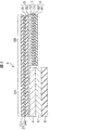
- FIG. 1 is a schematic plan view showing a biomedical electrode according to a first embodiment of the present invention.
- FIG. 2 is a schematic cross-sectional view taken along the line II-II in FIG.
- FIG. 3 is a schematic plan view showing a biological electrode according to the second embodiment of the present invention.
- 4 is a schematic cross-sectional view taken along line IV-IV in FIG.
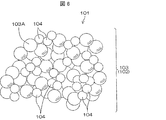
- FIG. 5 is a schematic diagram showing an example of a schematic particle structure of silica made of gelled silica.
- FIG. 6 is a schematic diagram schematically showing an example of a particle structure of silver chloride-supporting silica in which silver chloride is supported on silica made of gelled silica.
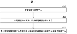
- FIG. 7 is a flowchart illustrating a method for forming a biomedical electrode.
- FIG. 1 is a schematic plan view showing a biomedical electrode according to a first embodiment of the present invention.
- FIG. 2 is a schematic cross-sectional view taken along the line II-II in FIG.
- the bioelectrode 1 includes a protective film 2, a main electrode film 3, an unpolarized electrode film 4, a conductive gel film 5, a release film 6, a lead wire 7, and a lead wire protective film 8. Yes.
- the protective film 2 includes a rectangular electrode protection portion 2A in plan view and a lead wire protection portion extending in one direction (right direction in FIG. 1) from the central portion of one side (right side in FIG. 1) of the electrode protection portion 2A. 2B.
- the protective film 2 includes a nonwoven fabric 21 and a resin film 22 formed on one surface (lower surface in FIG. 2) of the nonwoven fabric 81.
- the resin film 22 is made of polyethylene (PE).
- the main electrode film 3 has substantially the same planar shape as the protective film 2.
- the main electrode film 3 includes a base material 31 and a metal film 32 formed on one surface (the lower surface in FIG. 2) of the base material 31.
- the base material 31 is made of polyethylene terephthalate (PET)
- the metal film 32 is made of a silver vapor deposition film.
- Such a silver vapor deposition film can be formed by vapor-depositing silver on one surface of the substrate 31.
- the main electrode film 3 is bonded to one surface (lower surface in FIG. 2) of the protective film 2 with the surface (upper surface in FIG. 2) facing the base material 31 facing.
- the non-polarized electrode film 4 is formed on the surface of the main electrode film 3 opposite to the protective film 2 (the surface on the metal film 32 side) and in a region facing the electrode protection portion 2A of the protective film 2. .
- the non-polarized electrode film 4 is composed of an electrode film including a silver chloride carrier comprising a carrier and silver chloride carried on the carrier.
- Such an electrode film (unpolarized electrode film 4) can be formed from a silver chloride paste containing a silver chloride carrier. Details of the silver chloride paste containing the silver chloride carrier will be described later.
- the conductive gel film 5 is formed on almost the entire surface of the non-polarized electrode film 4 opposite to the main electrode film 3.
- the conductive gel film 5 is a part that directly contacts the skin of the living body when the bioelectrode 1 is used.
- the release film 6 is formed on almost the entire surface of the non-polarized electrode film 4 opposite to the main electrode film 3.
- the release film 6 is a release paper (release paper), a fluorine film, a polyethylene naphthalate (PEN) film in which a silicone or non-silicone (melamine, acrylic, etc.) release agent is applied on one or both sides, polyethylene A terephthalate (PET) film or the like is used.
- the release film 6 is peeled off when the biological electrode 1 is used.
- the lead wire 7 includes a strip-like base material 71 having a narrower width than the lead wire protection portion 2B of the protective film 2 in plan view, and a metal film 72 formed on one surface (upper surface in FIG. 2) of the base material 71. It consists of.
- the base material 71 is made of PET
- the metal film 72 is made of a silver vapor deposition film. Such a silver vapor deposition film can be formed by vapor-depositing silver on one surface of the substrate 71.
- the lead wire 7 is a surface of the main electrode film 3 opposite to the protective film 2 (the surface on the metal film 32 side, the lower surface in FIG. 2), and is in a region corresponding to the lead wire protection part 2B of the protective film 2. The bonding is performed with the metal film 72 side facing each other. The end of the lead wire 7 on the side of the electrode protection part 2A does not reach the electrode protection part 2A in a plan view and does not contact the non-polarized electrode film 4.
- the lead wire protective film 8 has substantially the same planar shape as the lead wire protective part 2B in the protective film 2.
- the lead wire protective film 8 includes a nonwoven fabric 81 and a resin film 82 formed on one surface of the nonwoven fabric 81 (upper surface in FIG. 2).
- the resin film 82 is made of PE.
- the lead wire protective film 8 is the surface of the main electrode film 3 opposite to the protective film 2 side (the surface on the metal film 32 side, the lower surface in FIG. 2), and corresponds to the lead wire protection part 2B of the protective film 2 In a state where the surface on the resin film 82 side is opposed to the region to be covered, the lead wire 7 is covered. Thereby, the lead wire 7 is covered with the protective film 2 mainly covering the upper surface of the lead wire 7 and the lead wire protective film 8 mainly covering the lower surface of the lead wire.
- the aforementioned living body electrode 1 is manufactured as follows, for example.
- An elongated rectangular protective film forming member (a member for forming the protective film 2) is prepared which is long in one direction in plan view and has a width equal to the width of the electrode protective portion 2A described above.
- an elongated rectangular lead wire protective film forming member (member for forming the lead wire protective film 8) having a long plan view in one direction and a width substantially equal to the width of the protective film forming member is prepared.
- a rectangular main electrode film forming member (a member for forming the main electrode film 3) having a rectangular shape in plan view and a width substantially equal to the width of the electrode protection portion 2A is prepared.
- the non-polarized electrode film 4 is formed on one end portion of the main electrode film forming member (the surface on the metal film side, the lower surface in FIG. 2) (the region corresponding to the electrode protection portion 2A of the protection film 2).
- a formed laminated electrode film is prepared.
- This laminated electrode film is, for example, formed in a silver chloride paste containing a silver chloride carrier on one end (surface on the metal film side) of one surface of the main electrode film forming member, and then included in the silver chloride paste. Produced by drying the solvent.
- the silver chloride paste can be formed on the main electrode film forming member by printing, transferring, coating, or the like.
- the solvent drying is performed by, for example, heat treatment at 110 ° C. for 3 minutes to 5 minutes.
- the thickness of the non-polarized electrode film 4 is, for example, an arbitrary thickness within the range of 1 ⁇ m to 100 ⁇ m, for example, 20 ⁇ m.
- membrane 5 was formed in one surface (FIG. 2 upper surface) of the peeling film 6 is prepared. Furthermore, a lead wire 7 is prepared. First, the laminated electrode film is bonded to one surface (the lower surface in FIG. 2) of the protective film forming member with the surface on the main electrode film forming member side facing. Next, a gel sheet with a release film is bonded to the surface of the laminated electrode film on the side of the nonpolarizing electrode film 4 with the surface on the side of the conductive gel film 5 facing.
- the lead wire 7 is placed on the surface of the main electrode film forming member opposite to the protective film forming member and in the region facing the lead wire protection portion planned region in the protective film forming member. Bonding is performed with the surface on the film 72 side (the upper surface in FIG. 2) facing each other.
- the lead wire is placed on the surface of the main electrode film forming member on the side to which the lead wire is bonded (the lower surface in FIG. 2) and in the region facing the lead wire protection portion planned region in the protective film forming member.
- the protective film forming member is bonded so as to cover the lead wire 7 with the surface on the resin film 82 side facing each other.
- the protective film forming member, the main electrode film forming member, and the lead wire protective film forming member are patterned so as to have the shapes of the protective film 2, the main electrode film 3, and the lead wire protective film 8, respectively.
- the biological electrode 1 shown in FIGS. 1 and 2 is obtained.
- the non-polarized electrode film 4 is composed of an electrode film including a silver chloride carrier composed of a carrier and silver chloride carried on the carrier. Therefore, when an unpolarized electrode film whose total amount of exposed area of silver chloride in the unpolarized electrode film 4 is a predetermined amount is obtained, the unpolarized electrode film containing silver / silver chloride described in Patent Document 1 As compared with the above, the total amount of silver can be reduced. Thereby, it is possible to reduce the cost while maintaining the nonpolarization property.
- the main electrode film 3 is composed of the base material 31 and the metal film 32 formed on one surface (the lower surface in FIG. 2) of the base material 31.
- membrane 3 may be comprised only from metal films, such as silver.
- the metal film 32 is composed of a silver vapor deposition film, but the metal film 32 may be a metal vapor deposition film other than silver.
- the metal film 32 may be a metal sputtered film formed by a sputtering method or a metal plated film formed by a plating method.
- FIG. 3 is a schematic plan view showing a biological electrode according to a second embodiment of the present invention. 4 is a schematic cross-sectional view taken along the line IV-IV in FIG.
- the biological electrode 1A according to the second embodiment is similar to the biological electrode 1 according to the first embodiment described above, and includes a protective film 2, a main electrode film 3A, an unpolarized electrode film 4, and a conductive material.
- the gel film 5, the release film 6, the lead wire 7, and the lead wire protective film 8 are included.
- the shape and the configuration of the protective film 2, the non-polarized electrode film 4, the conductive gel film 5, the release film 6, the lead wire 7 and the lead wire protective film 8 in the biological electrode 1A according to the second embodiment are respectively first.
- the shape and configuration of the protective film 2, the non-polarized electrode film 4, the conductive gel film 5, the release film 6, the lead wire 7, and the lead wire protective film 8 according to the embodiment are the same.
- the biological electrode 1A according to the second embodiment differs from the biological electrode 1 according to the first embodiment described above in the structure for attaching the lead wire 7 and the shape and material of the main electrode film 3A. ing.
- the main electrode film 3A has the same planar shape as the electrode protection part 2A of the protective film 2.
- the main electrode film 3 is composed of an electrode film containing silver.
- Such an electrode film can be formed from, for example, a silver paste (silver ink).
- the lead wire 7 is bonded to the surface of the protective film 2 on the resin film 22 side (the lower surface in FIG. 4) with the surface of the base material 71 facing the surface.
- the lead wires 7 are arranged so as to pass through the width central portion of the surface of the lead wire protection portion 2B of the protective film 2 on the resin film 22 side in plan view, but the electrode protection portion 2A of the lead wire 7 is disposed. One end portion on the side is disposed on the electrode protection portion 2A side beyond the lead wire protection portion 2B of the protective film 2.
- the nonpolarizing electrode film 4 is formed so as to cover one end of the lead wire 7 on almost the entire surface of the main electrode film 3A opposite to the protective film 2 (the lower surface in FIG. 4).
- the conductive gel film 5 is formed on almost the entire surface of the non-polarized electrode film 4 opposite to the main electrode film 3A.
- the release film 6 is formed on almost the entire surface of the non-polarized electrode film 4 opposite to the main electrode film 3A.
- the lead wire protective film 8 covers the lead wire 7 with the surface on the resin film 82 side facing the surface (the lower surface in FIG. 4) of the protective film 2 on which the lead wire 7 is formed. It is joined to. Thereby, the lead wire 7 is covered with the protective film 2 mainly covering the upper surface of the lead wire 7 and the lead wire protective film 8 mainly covering the lower surface of the lead wire.
- the biological electrode 1A described above is manufactured, for example, as follows.
- An elongated rectangular protective film forming member (a member for forming the protective film 2) is prepared which is long in one direction in plan view and has a width equal to the width of the electrode protective portion 2A described above.
- an elongated rectangular lead wire protective film forming member (a member for forming the lead wire protective film 8) having a long plan view in one direction and a width equal to the width of the protective film forming member is prepared.
- a laminated electrode film holding film in which a laminated film (laminated electrode film) of the main electrode film 3A and the non-polarized electrode film 4 is prepared on a polyester (PET) film substrate (not shown) is prepared.
- This laminated electrode film holding film is manufactured as follows, for example. That is, first, after forming a silver paste on a release film (not shown), the silver paste is dried to form the main electrode film 3A on the polyester film substrate. Then, after forming a silver chloride paste containing a silver chloride carrier on the surface of the main electrode film 3A, the silver chloride paste is dried to form the nonpolarized electrode film 4 on the main electrode film 3A. In this way, a laminated electrode film holding film is obtained.
- the thickness of the non-polarized electrode film 4 is, for example, an arbitrary thickness within the range of 1 ⁇ m to 100 ⁇ m, for example, 20 ⁇ m.
- the gel sheet with a peeling film in which the electroconductive gel film 5 was formed in one surface (upper surface in FIG. 4) of the peeling film 6 is prepared. Furthermore, a lead wire 7 is prepared. First, the lead wire 7 is bonded to one surface (the lower surface in FIG. 4) of the protective film forming member in a state where the surface on the substrate 71 side is opposed to the surface. At this time, most of the lead wire 7 passes through the width central portion of the surface of the lead wire protection portion 2B of the protection film 2 on the resin film 22 side, and one end portion of the lead wire 7 on the electrode protection portion 2A side is the lead wire protection portion. The lead wire 7 is disposed so as to protrude beyond 2B to the electrode protection portion 2A side.
- the polyester film substrate is peeled from the laminated electrode film holding film to obtain a laminated electrode film composed of the main electrode film 3A and the nonpolarized electrode film 4. Then, on one surface (the lower surface in FIG. 4) of the protective film forming member, the laminated electrode film is placed in a region corresponding to the electrode protection portion 2A, with the surface on the main electrode film 3A side facing. Then, bonding is performed so as to cover one end of the lead wire 7. Next, a gel sheet with a release film is bonded to the surface of the laminated electrode film on the side of the nonpolarizing electrode film 4 with the surface on the side of the conductive gel film 5 facing.
- the lead wire protective film is formed in a region facing the planned lead wire protection portion region in the protective film forming member.
- the forming member is joined so as to cover the lead wire 7 with the surface on the resin film 82 side facing each other.
- the protective film forming member and the lead wire protective film forming member are patterned so as to have the shapes of the protective film 2 and the lead wire protective film 8, respectively. Thereby, the biological electrode 1A shown in FIGS. 3 and 4 is obtained.
- the non-polarized electrode film 4 is composed of an electrode film including a silver chloride carrier composed of a carrier and silver chloride carried on the carrier. Therefore, when an unpolarized electrode film whose total amount of exposed area of silver chloride in the unpolarized electrode film 4 is a predetermined amount is obtained, the unpolarized electrode film containing silver / silver chloride described in Patent Document 1 As compared with the above, the total amount of silver can be reduced. Thereby, it is possible to reduce the cost while maintaining the nonpolarization property.
- the main electrode film 3 is made of an electrode film containing silver, but may be made of an electrode film containing carbon. Such an electrode film can be formed from a carbon paste.
- the main electrode film 3 may be formed from a conductive paste other than silver paste and carbon paste.
- Silver chloride paste for forming unpolarized electrode film is a silver chloride formed by supporting a binder resin and silver chloride on a carrier. A carrier. Since such a silver chloride paste contains a silver chloride carrier, it has nonpolarization properties.
- Binder Resin As the binder resin, for example, a thermoplastic resin can be used.
- polyester resin polyurethane resin, acrylic resin, alkyd resin, phenoxy resin, butyral resin, polyvinyl alcohol resin, or the like can be used as the binder resin.
- polyester resin include solvent-soluble polyesters TP-220, TP-217, TP-249, TP-235, TP-236, TP-290, TP-270, LP-manufactured by Nippon Synthetic Chemical Co., Ltd.
- the silver chloride carrier comprises a carrier and silver chloride carried on the carrier.
- Carrier As the material for the carrier, various materials such as metal (preferably a metal other than silver), nonmetal, organic matter, or inorganic matter can be used. In order to facilitate the dispersion of the silver chloride support in the binder resin, it is preferable not to precipitate the silver chloride support in the binder resin.
- the carrier preferably has a density close to that of the binder resin. Further, the carrier is more preferably a low-cost one that can easily carry silver chloride.
- the carrier includes (1) acrylic resin, polyurethane resin, polyester resin, or polyamide resin, (2) polymer particles made of epoxy resin, silica, mica, or glass beads, (3) calcium carbonate, etc. Inorganic particles consisting of can be used.
- Example 1 of silver chloride carrier is silver chloride-supported silica in which silver chloride is supported on silica (silicon dioxide).
- the silica on which silver chloride is supported may be wet method silica such as precipitation method silica or gelation method silica (gel method silica), or may be dry method silica.
- the silica is preferably gelled silica.
- the silica is gelled silica.
- FIG. 5 is a schematic diagram showing an example of a schematic particle structure of silica made of gelled silica.
- Silica 102 made of gelled silica has a particle structure in which, for example, a plurality of primary particles (skeleton particles) 103A gather in the shape of a bunch of grapes to form secondary particles 103.
- the specific surface area of silica refers to the surface area per unit mass.
- the surface area of silica is the sum of the external area and internal area of silica (the area of the pore inner surface of silica).
- the pore volume of silica refers to the volume of silica pores per unit mass.
- the average pore diameter of silica refers to the average diameter of silica pores (voids).
- the average particle diameter of silica refers to the average of the diameters D (see FIG. 5) of the secondary particles.
- the specific surface area of silica is preferably 20 m 2 / g or more and 1000 m 2 / g or less, and particularly preferably 100 m 2 / g or more and 700 m 2 / g or less.
- the pore volume of silica is preferably 0.2 ml / g or more and 2.0 ml / g or less, and particularly preferably 0.3 ml / g or more and 1.2 ml / g or less.
- the average pore diameter of silica is preferably 2 nm or more and 100 nm or less, and particularly preferably 2 nm or more and 30 nm or less.
- the average particle diameter of silica is preferably 1 ⁇ m or more and 50 ⁇ m or less, and particularly preferably 2 ⁇ m or more and 30 ⁇ m or less.
- FIG. 6 is a schematic diagram schematically showing an example of a particle structure of silver chloride-supporting silica in which silver chloride is supported on silica made of gelled silica.
- the silver chloride-supporting silica 101 shown in FIG. 6 includes silica 102 and silver chloride 104 supported on the surface of the silica 102 (including the content surface of the pores).
- the silver chloride-supporting silica is produced by the following production method. This manufacturing method includes the steps of generating a silver compound solution by dissolving the silver compound in the solution, and supporting the silver compound on silica (including the inner surface of the pores) using the silver compound solution. .
- As the silver compound silver nitrate or silver chloride is used.
- silver nitrate when silver nitrate is used as the silver compound, first, a silver nitrate solution is generated by dissolving silver nitrate powder in an aqueous solvent. Next, silver nitrate is supported on silica using a silver nitrate solution. Examples of the method for supporting silver nitrate on silica include a precipitation method, a gelation method, an impregnation method, and an ion exchange method. After that, silver chloride is supported on silica by reacting silver nitrate supported on silica with a compound containing chloride ions such as hydrochloric acid or sodium chloride.
- silver chloride when silver chloride is used as the silver compound, first, silver chloride powder is dissolved in an aqueous solution such as ammonia water, concentrated hydrochloric acid solution, alkaline cyanide aqueous solution, thiosulfate aqueous solution, or ammonium carbonate aqueous solution. To produce a silver chloride solution. Next, silver chloride is supported on silica using a silver chloride solution. Examples of the method for supporting silver chloride on silica include a precipitation method, a gelation method, an impregnation method, and an ion exchange method.
- an aqueous solution such as ammonia water, concentrated hydrochloric acid solution, alkaline cyanide aqueous solution, thiosulfate aqueous solution, or ammonium carbonate aqueous solution.
- an aqueous solution such as ammonia water, concentrated hydrochloric acid solution, alkaline cyanide aqueous solution, thiosulfate
- Example 1 of silver chloride-supported silica contains silica (Silicia 710 (trade name) manufactured by Fuji Silysia Chemical Co., Ltd.) that is a gelled silica and silver chloride (AgCl) supported on the silica.
- the content of silica (silicon dioxide) is 61% by weight and the silver chloride content is 39% by weight.
- the specific surface area of silica is 397 m 2 / g, and the average particle diameter of silica is 2.9 ⁇ m.
- Example 1 of silver chloride-supporting silica A method for producing Example 1 of silver chloride-supporting silica will be described.
- a silver nitrate solution was prepared by dissolving 40 g of silver nitrate powder with 50 ml of ion-exchanged water.
- 20 g of silica (Silicia 710 (trade name), manufactured by Fuji Silysia Chemical Ltd.) was added to the silver nitrate solution and stirred for 4 hours.
- the solid content was recovered from the stirred solution using 5 types A filter paper, and the recovered solid content was dried with a shelf dryer at 120 ° C. for 16 hours.
- silver nitrate-supporting silica in which silver nitrate was supported on silica was obtained.
- Another method for producing a silver chloride carrier The silver chloride carrier can also be produced by coating a carrier with silver and then subjecting it to a chlorination treatment.
- a method for coating the carrier with silver methods described in Patent Documents 2 and 3 can be used.
- Example of Method for Producing Silver Chloride Paste An example of a method for producing a silver chloride paste when the silver chloride carrier is silver chloride-supported silica will be described.
- 50 g of silver chloride-supporting silica powder was put in a container with a lid.
- the amount of silver chloride supported on the silver chloride-supported silica is an arbitrary amount within the range of 0.1 wt% to 80 wt%.
- 25 g of a mixed solvent of MEK (methyl ethyl ketone), ethyl acetate and toluene (mixing ratio 1: 1: 1) was put into the container and mixed with the silver chloride-supporting silica powder.
- 50 g of a binder resin solvent soluble type polyester LP-035 (solid content: 40%) manufactured by Nippon Synthetic Chemical Co., Ltd.
- stirring was performed for 10 minutes at a rotation speed of 3500 r / min. Thereby, the fluid silver chloride paste without powder aggregation was obtained.
- -Silver chloride has the property of being easy to aggregate (low dispersibility), while silica is hard to aggregate (high dispersibility). For this reason, silver chloride-supporting silica has higher dispersibility than silver chloride and is less likely to aggregate. Thereby, in a silver chloride paste using silver chloride-supporting silica, silver chloride (silver chloride-supporting silica) is less likely to aggregate. In the silver chloride-supporting silica, silver chloride is supported on silica (including the inner surface of the pores).
- the silver chloride paste using the silver chloride-supporting silica is compared with the conventional silver / silver chloride paste.
- the surface area of silver chloride can be increased.
- the polarization suppression effect can be improved.
- silver chloride-supporting silica silver chloride is supported on silica (including the inner surface of the pores).
- the main electrode film has a base material and a metal film formed on one surface of the base material.
- the biological electrode according to aspect 3 of the invention is the above-described aspect 1, wherein the main electrode film is made of a metal film.
- the biological electrode according to aspect 4 of the invention is the above-described aspect 2 or 3, wherein the metal film is one arbitrarily selected from a metal vapor deposition film, a metal sputtered film, and a metal plating film.
- the metal film is made of silver.
- the biological electrode according to aspect 6 of the present invention is the above-described aspect 1, wherein the main electrode film is composed of an electrode film containing silver or an electrode film containing carbon.
- a biological electrode according to aspect 7 of the invention further includes a protective film formed on the surface of the main electrode film opposite to the non-polarized electrode film in any of the above aspects 1 to 6.
- the biological electrode according to Aspect 8 of the invention further includes a release film formed on the surface of the conductive gel film opposite to the non-polarized electrode film in any one of Aspects 1 to 7.
- the carrier is silica.
- a biological electrode according to aspect 10 of the present invention further includes a lead wire having one end electrically connected to the main electrode film in any of the above aspects 1 to 9.
- a biological electrode according to an eleventh aspect of the invention includes, in order, a main electrode film, an unpolarized electrode film, and a conductive gel film, and the unpolarized electrode film includes a carrier and silver chloride supported on the carrier. It is comprised from the electrode film containing the silver chloride support body which has this.
- the biological electrode forming method according to the twelfth aspect of the present invention includes a step of forming a main electrode film (S10), a step of forming an unpolarized electrode film on one surface of the main electrode film (S20), and the non-polarization.
- the electrode film includes a silver chloride carrier having silver chloride.
- the biological electrode forming method according to the thirteenth aspect of the invention includes a step of forming a main electrode film (S10), a step of forming a conductive gel film on one surface of the main electrode film (S20), and the conductive Forming an unpolarized electrode film on the surface of the gel film opposite to the side on which the main electrode film is formed (S30), and the unpolarized electrode film is supported on the carrier and the carrier
- the electrode film includes a silver chloride carrier having silver chloride.
Abstract
La présente invention concerne une bioélectrode (1) comprenant : une couche d'électrode principale (3); une couche d'électrode non polarisable (4) formée sur une surface de la couche d'électrode principale (3); et une couche de gel conducteur (5) formée sur une surface de la couche d'électrode non polarisable (4) se trouvant à l'opposé de la couche d'électrode principale. La couche d'électrode non polarisable (4) comprend une couche d'électrode qui comprend un support au chlorure d'argent comprenant un substrat et du chlorure d'argent supporté par celui-ci.
Priority Applications (3)
| Application Number | Priority Date | Filing Date | Title |
|---|---|---|---|
| CN201780038347.7A CN109414210B (zh) | 2016-06-30 | 2017-06-23 | 生物体用电极、以及生物体用电极的形成方法 |
| US16/311,334 US11490846B2 (en) | 2016-06-30 | 2017-06-23 | Bioelectrode and method for producing bioelectrode |
| JP2018525134A JP6785856B2 (ja) | 2016-06-30 | 2017-06-23 | 生体用電極、及び生体用電極の形成方法 |
Applications Claiming Priority (2)
| Application Number | Priority Date | Filing Date | Title |
|---|---|---|---|
| JP2016-130503 | 2016-06-30 | ||
| JP2016130503 | 2016-06-30 |
Publications (1)
| Publication Number | Publication Date |
|---|---|
| WO2018003697A1 true WO2018003697A1 (fr) | 2018-01-04 |
Family
ID=60786368
Family Applications (1)
| Application Number | Title | Priority Date | Filing Date |
|---|---|---|---|
| PCT/JP2017/023226 WO2018003697A1 (fr) | 2016-06-30 | 2017-06-23 | Bioélectrode et procédé de production de bioélectrode |
Country Status (4)
| Country | Link |
|---|---|
| US (1) | US11490846B2 (fr) |
| JP (1) | JP6785856B2 (fr) |
| CN (1) | CN109414210B (fr) |
| WO (1) | WO2018003697A1 (fr) |
Cited By (3)
| Publication number | Priority date | Publication date | Assignee | Title |
|---|---|---|---|---|
| WO2021181752A1 (fr) * | 2020-03-13 | 2021-09-16 | タツタ電線株式会社 | Bioélectrode |
| CN113613902A (zh) * | 2019-03-19 | 2021-11-05 | 东丽株式会社 | 导电性片材 |
| WO2022107784A1 (fr) * | 2020-11-17 | 2022-05-27 | タツタ電線株式会社 | Bioélectrode |
Families Citing this family (2)
| Publication number | Priority date | Publication date | Assignee | Title |
|---|---|---|---|---|
| JP6727399B2 (ja) * | 2017-03-07 | 2020-07-22 | アルプスアルパイン株式会社 | 生体情報測定用電極及び生体情報測定用電極の製造方法 |
| EP4344639A1 (fr) | 2022-09-30 | 2024-04-03 | Ambu A/S | Elément de détection d'argent/chlorure d'argent |
Citations (8)
| Publication number | Priority date | Publication date | Assignee | Title |
|---|---|---|---|---|
| JPS5126789A (en) * | 1974-08-29 | 1976-03-05 | Richaado Sato Takuya | Gin enkagindenkyoku |
| JPS5721302U (fr) * | 1980-07-09 | 1982-02-03 | ||
| JPS587227A (ja) * | 1981-07-02 | 1983-01-17 | ティーディーケイ株式会社 | 生体用電極の製造方法 |
| JPS59190649A (ja) * | 1983-04-14 | 1984-10-29 | Terumo Corp | 基準電極 |
| JPH0595922A (ja) * | 1991-10-08 | 1993-04-20 | Nippon Achison Kk | 生体用電極およびその製造方法 |
| JP2001292972A (ja) * | 2000-04-13 | 2001-10-23 | Nippon Koden Corp | 生体用電極 |
| WO2007111368A1 (fr) * | 2006-03-29 | 2007-10-04 | Tti Ellebeau, Inc. | Appareil iontophorétique |
| JP2014517759A (ja) * | 2011-05-23 | 2014-07-24 | エスエイチエル・テレメデイシン・インターナシヨナル・リミテツド | 心電図監視システムおよび方法 |
Family Cites Families (57)
| Publication number | Priority date | Publication date | Assignee | Title |
|---|---|---|---|---|
| JPS5319870A (en) | 1976-08-06 | 1978-02-23 | Seiko Epson Corp | Structure of digital watch |
| DE2940529A1 (de) * | 1978-10-06 | 1980-04-17 | Tdk Electronics Co Ltd | Silber-silberchlorid-elektrode |
| US4377170A (en) | 1980-12-01 | 1983-03-22 | Minnesota Mining And Manufacturing Company | Non-polarizable bioelectrode |
| JPS6410164A (en) | 1987-07-03 | 1989-01-13 | Terumo Corp | Reference electrode |
| US4852571A (en) * | 1987-09-03 | 1989-08-01 | Marquette Electronics | Disposable biopotential electrode |
| JPH05182513A (ja) | 1991-12-27 | 1993-07-23 | Tokuriki Honten Co Ltd | 厚膜形成用ペーストおよび厚膜の形成方法 |
| JPH05176904A (ja) | 1991-12-27 | 1993-07-20 | Tokuriki Honten Co Ltd | 銀−塩化銀電極およびその製造方法 |
| JP3149597B2 (ja) * | 1993-02-03 | 2001-03-26 | 松下電器産業株式会社 | 体液成分測定装置 |
| US5506059A (en) | 1993-05-14 | 1996-04-09 | Minnesota Mining And Manufacturing Company | Metallic films and articles using same |
| US5505200A (en) | 1994-01-28 | 1996-04-09 | Minnesota Mining And Manufacturing | Biomedical conductor containing inorganic oxides and biomedical electrodes prepared therefrom |
| US5565143A (en) | 1995-05-05 | 1996-10-15 | E. I. Du Pont De Nemours And Company | Water-based silver-silver chloride compositions |
| US5851438A (en) | 1997-08-29 | 1998-12-22 | E. I. Du Pont De Nemours And Company | Thick film compositions for making medical electrodes |
| WO2001004614A1 (fr) | 1999-07-13 | 2001-01-18 | Wakunaga Pharmaceutical Co., Ltd. | Biocapteur electrochimique avec electrode d'argent-chlorure d'argent et matrice de chromatographie |
| US6623664B2 (en) * | 1999-12-24 | 2003-09-23 | 3M Innovative Properties Company | Conductive adhesive and biomedical electrode |
| ATE468531T1 (de) | 2001-05-30 | 2010-06-15 | I Sens Inc | Biosensor |
| US6702968B2 (en) | 2001-09-17 | 2004-03-09 | Michael J. Stevenson | Printed circuit techniques for polyethylene surfaces |
| JP4278020B2 (ja) | 2001-10-30 | 2009-06-10 | 日揮触媒化成株式会社 | 研磨用粒子および研磨材の製造方法 |
| CN1228395C (zh) | 2002-05-20 | 2005-11-23 | 中国科学院理化技术研究所 | 微介孔二氧化硅异质复合体及其制备方法和用途 |
| CN1274593C (zh) | 2003-11-25 | 2006-09-13 | 复旦大学 | 一种有序介孔氧化硅单片材料的制备方法 |
| US20100185071A1 (en) | 2003-12-05 | 2010-07-22 | Dexcom, Inc. | Dual electrode system for a continuous analyte sensor |
| CN1286923C (zh) | 2004-03-03 | 2006-11-29 | 中国科学院理化技术研究所 | 释放负离子的抗菌纳米负载材料及其制备方法和用途 |
| CN2685874Y (zh) | 2004-03-17 | 2005-03-16 | 武汉大学 | 高温全密封式参比电极 |
| JP2007085763A (ja) | 2005-09-20 | 2007-04-05 | Citizen Watch Co Ltd | 濃度測定装置 |
| CN100364884C (zh) * | 2006-01-26 | 2008-01-30 | 复旦大学 | 一种介孔碳材料的制备方法 |
| CN101081699B (zh) | 2006-05-31 | 2010-04-14 | 南京理工大学 | 一种有序介孔氧化硅及其快速制备方法 |
| US20080177166A1 (en) | 2007-01-18 | 2008-07-24 | Provex Technologies, Llc | Ultrasensitive amperometric saliva glucose sensor strip |
| CN101037220B (zh) | 2007-02-15 | 2011-06-01 | 中国科学院上海硅酸盐研究所 | 一种具有高比表面积的片状钠/锂-锰材料及其制备方法 |
| JP4466674B2 (ja) | 2007-03-30 | 2010-05-26 | Tdk株式会社 | 電極及び電気化学デバイス |
| CN100515986C (zh) | 2007-09-06 | 2009-07-22 | 哈尔滨工业大学 | 一种抑菌陶粒及其制备方法 |
| CN101420032B (zh) | 2007-10-26 | 2011-12-14 | 比亚迪股份有限公司 | 一种组合物浆料、其制备方法及其应用 |
| TW201004869A (en) | 2008-06-10 | 2010-02-01 | Nanotune Technologies Corp | Nanoporous materials and related methods |
| WO2010020007A1 (fr) | 2008-08-20 | 2010-02-25 | The University Of Queensland | Électrodes en carbone nanoporeux et supercondensateurs formés à partir de celles-ci |
| CN101435792B (zh) | 2008-12-17 | 2012-05-30 | 中国科学院上海硅酸盐研究所 | 氮掺杂介孔碳固定化酶生物传感材料及其制备方法 |
| CN102198929B (zh) | 2010-03-22 | 2013-05-01 | 中国科学院理化技术研究所 | 具有纳米级贵金属和二氧化硅内核的中空二氧化硅亚微米球及其制备方法 |
| CN102285659B (zh) | 2010-06-17 | 2013-04-03 | 国家纳米科学中心 | 一种有序介孔二氧化硅材料及其制备方法 |
| CN103189131A (zh) | 2010-08-06 | 2013-07-03 | 台达电子工业股份有限公司 | 多孔材料的制造方法 |
| JP2012091358A (ja) | 2010-10-26 | 2012-05-17 | Sumitomo Chemical Co Ltd | 押出成形機とこれを用いる成形体の製造方法 |
| EP2465426A1 (fr) | 2010-12-20 | 2012-06-20 | General Electric Company | Capteur biomédical |
| CN102091331B (zh) | 2011-01-19 | 2012-11-21 | 浙江大学 | 一种羧基化介孔二氧化硅纳米粒载体材料及制备方法 |
| KR101812370B1 (ko) | 2011-05-31 | 2017-12-26 | 다츠다 덴센 가부시키가이샤 | 접착제 조성물 및 접착 필름 |
| CN102380334A (zh) | 2011-07-25 | 2012-03-21 | 重庆文理学院 | 一种具三维孔道结构的介孔高分子或碳/氧化硅纳米复合材料及其制备方法 |
| CN102976457A (zh) | 2012-11-08 | 2013-03-20 | 赵建树 | 负载纳米银的有机功能化二氧化硅、其制备方法及其应用 |
| JP5915555B2 (ja) | 2013-01-28 | 2016-05-11 | 富士ゼロックス株式会社 | シリカ複合粒子及びその製造方法 |
| WO2014129597A1 (fr) | 2013-02-21 | 2014-08-28 | 新日鉄住金化学株式会社 | Matière de carbone en vue d'une utilisation comme support de catalyseur |
| CN103149258B (zh) | 2013-02-26 | 2015-09-23 | 山东大学 | 一种基于纳米多孔金-导电聚合物的生物电极的制备方法 |
| CN103192070B (zh) | 2013-04-17 | 2015-07-08 | 苏州格林泰克科技有限公司 | 一种银/氯化银电极材料及其制备方法和电极 |
| CN103783081A (zh) | 2014-01-17 | 2014-05-14 | 浙江理工大学 | 一种银-氧化铜共掺杂的介孔二氧化锆抗菌剂的制备方法 |
| CN103798289A (zh) | 2014-02-14 | 2014-05-21 | 浙江理工大学 | 一种载银介孔二氧化硅抗菌剂的制备方法 |
| CN103861657B (zh) | 2014-02-24 | 2015-07-08 | 浙江大学 | 纳米银负载多孔二氧化硅的制备方法 |
| JP6429228B2 (ja) | 2014-04-24 | 2018-11-28 | タツタ電線株式会社 | 金属被覆樹脂粒子及びそれを用いた導電性接着剤 |
| CN204306820U (zh) | 2014-11-10 | 2015-05-06 | 青岛柏恩鸿泰电子科技有限公司 | 一种银/氯化银粉末电极 |
| WO2017031487A1 (fr) | 2015-08-20 | 2017-02-23 | Parker-Hannifin Corporation | Compositions argent-chlorure d'argent et dispositifs électriques les contenant |
| CN105334250A (zh) | 2015-10-23 | 2016-02-17 | 吴国清 | 一种银/氯化银电极片及其制备工艺 |
| CN105581793A (zh) | 2016-01-29 | 2016-05-18 | 上海傲意信息科技有限公司 | 一种人体生物电监测服装 |
| CN109310355B (zh) * | 2016-06-30 | 2022-03-22 | 拓自达电线株式会社 | 电极材料 |
| WO2018003702A1 (fr) * | 2016-06-30 | 2018-01-04 | タツタ電線株式会社 | Pâte de chlorure d'argent. |
| JP6654164B2 (ja) | 2017-03-30 | 2020-02-26 | タツタ電線株式会社 | 塩化銀被覆粒子 |
-
2017
- 2017-06-23 WO PCT/JP2017/023226 patent/WO2018003697A1/fr active Application Filing
- 2017-06-23 CN CN201780038347.7A patent/CN109414210B/zh active Active
- 2017-06-23 US US16/311,334 patent/US11490846B2/en active Active
- 2017-06-23 JP JP2018525134A patent/JP6785856B2/ja active Active
Patent Citations (8)
| Publication number | Priority date | Publication date | Assignee | Title |
|---|---|---|---|---|
| JPS5126789A (en) * | 1974-08-29 | 1976-03-05 | Richaado Sato Takuya | Gin enkagindenkyoku |
| JPS5721302U (fr) * | 1980-07-09 | 1982-02-03 | ||
| JPS587227A (ja) * | 1981-07-02 | 1983-01-17 | ティーディーケイ株式会社 | 生体用電極の製造方法 |
| JPS59190649A (ja) * | 1983-04-14 | 1984-10-29 | Terumo Corp | 基準電極 |
| JPH0595922A (ja) * | 1991-10-08 | 1993-04-20 | Nippon Achison Kk | 生体用電極およびその製造方法 |
| JP2001292972A (ja) * | 2000-04-13 | 2001-10-23 | Nippon Koden Corp | 生体用電極 |
| WO2007111368A1 (fr) * | 2006-03-29 | 2007-10-04 | Tti Ellebeau, Inc. | Appareil iontophorétique |
| JP2014517759A (ja) * | 2011-05-23 | 2014-07-24 | エスエイチエル・テレメデイシン・インターナシヨナル・リミテツド | 心電図監視システムおよび方法 |
Cited By (5)
| Publication number | Priority date | Publication date | Assignee | Title |
|---|---|---|---|---|
| CN113613902A (zh) * | 2019-03-19 | 2021-11-05 | 东丽株式会社 | 导电性片材 |
| CN113613902B (zh) * | 2019-03-19 | 2023-08-18 | 东丽株式会社 | 导电性片材 |
| WO2021181752A1 (fr) * | 2020-03-13 | 2021-09-16 | タツタ電線株式会社 | Bioélectrode |
| WO2022107784A1 (fr) * | 2020-11-17 | 2022-05-27 | タツタ電線株式会社 | Bioélectrode |
| JP7119252B1 (ja) * | 2020-11-17 | 2022-08-16 | タツタ電線株式会社 | 生体用電極 |
Also Published As
| Publication number | Publication date |
|---|---|
| JPWO2018003697A1 (ja) | 2019-04-18 |
| CN109414210A (zh) | 2019-03-01 |
| CN109414210B (zh) | 2022-03-11 |
| JP6785856B2 (ja) | 2020-11-18 |
| US20190320923A1 (en) | 2019-10-24 |
| US11490846B2 (en) | 2022-11-08 |
Similar Documents
| Publication | Publication Date | Title |
|---|---|---|
| WO2018003697A1 (fr) | Bioélectrode et procédé de production de bioélectrode | |
| CN100505323C (zh) | 电极、光电转换元件和染料增感太阳能电池 | |
| KR101861235B1 (ko) | 은나노와이어를 포함하는 전도막, 발열체 및 그의 제조 방법 | |
| JP6612984B2 (ja) | 塩化銀ペースト | |
| Wang et al. | Enhanced photo-electrocatalytic performance of Pt/RGO/TiO 2 on carbon fiber towards methanol oxidation in alkaline media | |
| JP6069991B2 (ja) | ペロブスカイト化合物を用いた光電変換素子の製造方法 | |
| JP2017531046A (ja) | Ldsプラスチックのための添加剤 | |
| JP2014049551A (ja) | ペロブスカイト化合物を用いた光電変換素子およびその製造方法 | |
| WO2016101982A1 (fr) | Nanotubes de carbone multi-fonctionnalisés | |
| JP2014229747A (ja) | ペロブスカイト化合物を用いた光電変換素子およびその製造方法 | |
| JP6082007B2 (ja) | 光電変換層用組成物および光電変換素子 | |
| CN113758975A (zh) | 一种激光诱导的石墨烯/金属氧化物敏感材料及其制备方法 | |
| KR20170045669A (ko) | 도전체, 그 제조 방법, 및 이를 포함하는 소자 | |
| CN112105248A (zh) | 一种电磁屏蔽膜及其制备方法 | |
| Dalagan et al. | Simultaneous functionalization and reduction of graphene oxide with diatom silica | |
| KR101802932B1 (ko) | 면상발열체와, 면상발열체의 제조방법 | |
| JP5348962B2 (ja) | 光電気セルの製造方法 | |
| CN109843809A (zh) | 金属被覆粒子及树脂组合物 | |
| KR101826149B1 (ko) | 투명 면상 발열체 | |
| CN217470312U (zh) | 透明薄膜加热器及应用该透明薄膜加热器的产品 | |
| JP5960989B2 (ja) | 酸化チタン含有多孔質膜積層体及びその製造方法 | |
| JP2010153232A (ja) | 多孔質半導体膜形成用塗料および光電気セル | |
| CN112499684B (zh) | 一种基于离子斥力作用分散剥离多层wo3纳米片的方法 | |
| CN109860337A (zh) | 一种耐高温柔性透明电极的制备方法 | |
| JP5432486B2 (ja) | 多孔質膜及びこれを用いた透明電極 |
Legal Events
| Date | Code | Title | Description |
|---|---|---|---|
| ENP | Entry into the national phase |
Ref document number: 2018525134 Country of ref document: JP Kind code of ref document: A |
|
| 121 | Ep: the epo has been informed by wipo that ep was designated in this application |
Ref document number: 17820054 Country of ref document: EP Kind code of ref document: A1 |
|
| NENP | Non-entry into the national phase |
Ref country code: DE |
|
| 122 | Ep: pct application non-entry in european phase |
Ref document number: 17820054 Country of ref document: EP Kind code of ref document: A1 |