WO2018003697A1 - Bioelectrode and method for producing bioelectrode - Google Patents
Bioelectrode and method for producing bioelectrode Download PDFInfo
- Publication number
- WO2018003697A1 WO2018003697A1 PCT/JP2017/023226 JP2017023226W WO2018003697A1 WO 2018003697 A1 WO2018003697 A1 WO 2018003697A1 JP 2017023226 W JP2017023226 W JP 2017023226W WO 2018003697 A1 WO2018003697 A1 WO 2018003697A1
- Authority
- WO
- WIPO (PCT)
- Prior art keywords
- film
- electrode film
- electrode
- silver chloride
- silver
- Prior art date
Links
Images


Classifications
-
- B—PERFORMING OPERATIONS; TRANSPORTING
- B32—LAYERED PRODUCTS
- B32B—LAYERED PRODUCTS, i.e. PRODUCTS BUILT-UP OF STRATA OF FLAT OR NON-FLAT, e.g. CELLULAR OR HONEYCOMB, FORM
- B32B3/00—Layered products comprising a layer with external or internal discontinuities or unevennesses, or a layer of non-planar form; Layered products having particular features of form
- B32B3/02—Layered products comprising a layer with external or internal discontinuities or unevennesses, or a layer of non-planar form; Layered products having particular features of form characterised by features of form at particular places, e.g. in edge regions
- B32B3/08—Layered products comprising a layer with external or internal discontinuities or unevennesses, or a layer of non-planar form; Layered products having particular features of form characterised by features of form at particular places, e.g. in edge regions characterised by added members at particular parts
-
- A—HUMAN NECESSITIES
- A61—MEDICAL OR VETERINARY SCIENCE; HYGIENE
- A61B—DIAGNOSIS; SURGERY; IDENTIFICATION
- A61B5/00—Measuring for diagnostic purposes; Identification of persons
- A61B5/24—Detecting, measuring or recording bioelectric or biomagnetic signals of the body or parts thereof
- A61B5/25—Bioelectric electrodes therefor
- A61B5/279—Bioelectric electrodes therefor specially adapted for particular uses
- A61B5/291—Bioelectric electrodes therefor specially adapted for particular uses for electroencephalography [EEG]
-
- B—PERFORMING OPERATIONS; TRANSPORTING
- B32—LAYERED PRODUCTS
- B32B—LAYERED PRODUCTS, i.e. PRODUCTS BUILT-UP OF STRATA OF FLAT OR NON-FLAT, e.g. CELLULAR OR HONEYCOMB, FORM
- B32B1/00—Layered products having a general shape other than plane
- B32B1/08—Tubular products
-
- B—PERFORMING OPERATIONS; TRANSPORTING
- B32—LAYERED PRODUCTS
- B32B—LAYERED PRODUCTS, i.e. PRODUCTS BUILT-UP OF STRATA OF FLAT OR NON-FLAT, e.g. CELLULAR OR HONEYCOMB, FORM
- B32B15/00—Layered products comprising a layer of metal
- B32B15/04—Layered products comprising a layer of metal comprising metal as the main or only constituent of a layer, which is next to another layer of the same or of a different material
- B32B15/046—Layered products comprising a layer of metal comprising metal as the main or only constituent of a layer, which is next to another layer of the same or of a different material of foam
-
- B—PERFORMING OPERATIONS; TRANSPORTING
- B32—LAYERED PRODUCTS
- B32B—LAYERED PRODUCTS, i.e. PRODUCTS BUILT-UP OF STRATA OF FLAT OR NON-FLAT, e.g. CELLULAR OR HONEYCOMB, FORM
- B32B15/00—Layered products comprising a layer of metal
- B32B15/04—Layered products comprising a layer of metal comprising metal as the main or only constituent of a layer, which is next to another layer of the same or of a different material
- B32B15/08—Layered products comprising a layer of metal comprising metal as the main or only constituent of a layer, which is next to another layer of the same or of a different material of synthetic resin
- B32B15/09—Layered products comprising a layer of metal comprising metal as the main or only constituent of a layer, which is next to another layer of the same or of a different material of synthetic resin comprising polyesters
-
- B—PERFORMING OPERATIONS; TRANSPORTING
- B32—LAYERED PRODUCTS
- B32B—LAYERED PRODUCTS, i.e. PRODUCTS BUILT-UP OF STRATA OF FLAT OR NON-FLAT, e.g. CELLULAR OR HONEYCOMB, FORM
- B32B27/00—Layered products comprising a layer of synthetic resin
- B32B27/06—Layered products comprising a layer of synthetic resin as the main or only constituent of a layer, which is next to another layer of the same or of a different material
- B32B27/065—Layered products comprising a layer of synthetic resin as the main or only constituent of a layer, which is next to another layer of the same or of a different material of foam
-
- B—PERFORMING OPERATIONS; TRANSPORTING
- B32—LAYERED PRODUCTS
- B32B—LAYERED PRODUCTS, i.e. PRODUCTS BUILT-UP OF STRATA OF FLAT OR NON-FLAT, e.g. CELLULAR OR HONEYCOMB, FORM
- B32B27/00—Layered products comprising a layer of synthetic resin
- B32B27/06—Layered products comprising a layer of synthetic resin as the main or only constituent of a layer, which is next to another layer of the same or of a different material
- B32B27/08—Layered products comprising a layer of synthetic resin as the main or only constituent of a layer, which is next to another layer of the same or of a different material of synthetic resin
-
- B—PERFORMING OPERATIONS; TRANSPORTING
- B32—LAYERED PRODUCTS
- B32B—LAYERED PRODUCTS, i.e. PRODUCTS BUILT-UP OF STRATA OF FLAT OR NON-FLAT, e.g. CELLULAR OR HONEYCOMB, FORM
- B32B27/00—Layered products comprising a layer of synthetic resin
- B32B27/12—Layered products comprising a layer of synthetic resin next to a fibrous or filamentary layer
-
- B—PERFORMING OPERATIONS; TRANSPORTING
- B32—LAYERED PRODUCTS
- B32B—LAYERED PRODUCTS, i.e. PRODUCTS BUILT-UP OF STRATA OF FLAT OR NON-FLAT, e.g. CELLULAR OR HONEYCOMB, FORM
- B32B27/00—Layered products comprising a layer of synthetic resin
- B32B27/30—Layered products comprising a layer of synthetic resin comprising vinyl (co)polymers; comprising acrylic (co)polymers
- B32B27/308—Layered products comprising a layer of synthetic resin comprising vinyl (co)polymers; comprising acrylic (co)polymers comprising acrylic (co)polymers
-
- B—PERFORMING OPERATIONS; TRANSPORTING
- B32—LAYERED PRODUCTS
- B32B—LAYERED PRODUCTS, i.e. PRODUCTS BUILT-UP OF STRATA OF FLAT OR NON-FLAT, e.g. CELLULAR OR HONEYCOMB, FORM
- B32B27/00—Layered products comprising a layer of synthetic resin
- B32B27/32—Layered products comprising a layer of synthetic resin comprising polyolefins
-
- B—PERFORMING OPERATIONS; TRANSPORTING
- B32—LAYERED PRODUCTS
- B32B—LAYERED PRODUCTS, i.e. PRODUCTS BUILT-UP OF STRATA OF FLAT OR NON-FLAT, e.g. CELLULAR OR HONEYCOMB, FORM
- B32B27/00—Layered products comprising a layer of synthetic resin
- B32B27/34—Layered products comprising a layer of synthetic resin comprising polyamides
-
- B—PERFORMING OPERATIONS; TRANSPORTING
- B32—LAYERED PRODUCTS
- B32B—LAYERED PRODUCTS, i.e. PRODUCTS BUILT-UP OF STRATA OF FLAT OR NON-FLAT, e.g. CELLULAR OR HONEYCOMB, FORM
- B32B27/00—Layered products comprising a layer of synthetic resin
- B32B27/36—Layered products comprising a layer of synthetic resin comprising polyesters
-
- B—PERFORMING OPERATIONS; TRANSPORTING
- B32—LAYERED PRODUCTS
- B32B—LAYERED PRODUCTS, i.e. PRODUCTS BUILT-UP OF STRATA OF FLAT OR NON-FLAT, e.g. CELLULAR OR HONEYCOMB, FORM
- B32B27/00—Layered products comprising a layer of synthetic resin
- B32B27/40—Layered products comprising a layer of synthetic resin comprising polyurethanes
-
- B—PERFORMING OPERATIONS; TRANSPORTING
- B32—LAYERED PRODUCTS
- B32B—LAYERED PRODUCTS, i.e. PRODUCTS BUILT-UP OF STRATA OF FLAT OR NON-FLAT, e.g. CELLULAR OR HONEYCOMB, FORM
- B32B29/00—Layered products comprising a layer of paper or cardboard
- B32B29/002—Layered products comprising a layer of paper or cardboard as the main or only constituent of a layer, which is next to another layer of the same or of a different material
- B32B29/007—Layered products comprising a layer of paper or cardboard as the main or only constituent of a layer, which is next to another layer of the same or of a different material next to a foam layer
-
- B—PERFORMING OPERATIONS; TRANSPORTING
- B32—LAYERED PRODUCTS
- B32B—LAYERED PRODUCTS, i.e. PRODUCTS BUILT-UP OF STRATA OF FLAT OR NON-FLAT, e.g. CELLULAR OR HONEYCOMB, FORM
- B32B5/00—Layered products characterised by the non- homogeneity or physical structure, i.e. comprising a fibrous, filamentary, particulate or foam layer; Layered products characterised by having a layer differing constitutionally or physically in different parts
- B32B5/02—Layered products characterised by the non- homogeneity or physical structure, i.e. comprising a fibrous, filamentary, particulate or foam layer; Layered products characterised by having a layer differing constitutionally or physically in different parts characterised by structural features of a fibrous or filamentary layer
- B32B5/022—Non-woven fabric
-
- B—PERFORMING OPERATIONS; TRANSPORTING
- B32—LAYERED PRODUCTS
- B32B—LAYERED PRODUCTS, i.e. PRODUCTS BUILT-UP OF STRATA OF FLAT OR NON-FLAT, e.g. CELLULAR OR HONEYCOMB, FORM
- B32B5/00—Layered products characterised by the non- homogeneity or physical structure, i.e. comprising a fibrous, filamentary, particulate or foam layer; Layered products characterised by having a layer differing constitutionally or physically in different parts
- B32B5/16—Layered products characterised by the non- homogeneity or physical structure, i.e. comprising a fibrous, filamentary, particulate or foam layer; Layered products characterised by having a layer differing constitutionally or physically in different parts characterised by features of a layer formed of particles, e.g. chips, powder or granules
-
- B—PERFORMING OPERATIONS; TRANSPORTING
- B32—LAYERED PRODUCTS
- B32B—LAYERED PRODUCTS, i.e. PRODUCTS BUILT-UP OF STRATA OF FLAT OR NON-FLAT, e.g. CELLULAR OR HONEYCOMB, FORM
- B32B5/00—Layered products characterised by the non- homogeneity or physical structure, i.e. comprising a fibrous, filamentary, particulate or foam layer; Layered products characterised by having a layer differing constitutionally or physically in different parts
- B32B5/18—Layered products characterised by the non- homogeneity or physical structure, i.e. comprising a fibrous, filamentary, particulate or foam layer; Layered products characterised by having a layer differing constitutionally or physically in different parts characterised by features of a layer of foamed material
-
- B—PERFORMING OPERATIONS; TRANSPORTING
- B32—LAYERED PRODUCTS
- B32B—LAYERED PRODUCTS, i.e. PRODUCTS BUILT-UP OF STRATA OF FLAT OR NON-FLAT, e.g. CELLULAR OR HONEYCOMB, FORM
- B32B7/00—Layered products characterised by the relation between layers; Layered products characterised by the relative orientation of features between layers, or by the relative values of a measurable parameter between layers, i.e. products comprising layers having different physical, chemical or physicochemical properties; Layered products characterised by the interconnection of layers
- B32B7/04—Interconnection of layers
- B32B7/06—Interconnection of layers permitting easy separation
-
- C—CHEMISTRY; METALLURGY
- C09—DYES; PAINTS; POLISHES; NATURAL RESINS; ADHESIVES; COMPOSITIONS NOT OTHERWISE PROVIDED FOR; APPLICATIONS OF MATERIALS NOT OTHERWISE PROVIDED FOR
- C09J—ADHESIVES; NON-MECHANICAL ASPECTS OF ADHESIVE PROCESSES IN GENERAL; ADHESIVE PROCESSES NOT PROVIDED FOR ELSEWHERE; USE OF MATERIALS AS ADHESIVES
- C09J9/00—Adhesives characterised by their physical nature or the effects produced, e.g. glue sticks
- C09J9/02—Electrically-conducting adhesives
-
- A—HUMAN NECESSITIES
- A61—MEDICAL OR VETERINARY SCIENCE; HYGIENE
- A61B—DIAGNOSIS; SURGERY; IDENTIFICATION
- A61B2562/00—Details of sensors; Constructional details of sensor housings or probes; Accessories for sensors
- A61B2562/02—Details of sensors specially adapted for in-vivo measurements
- A61B2562/0209—Special features of electrodes classified in A61B5/24, A61B5/25, A61B5/283, A61B5/291, A61B5/296, A61B5/053
- A61B2562/0215—Silver or silver chloride containing
-
- A—HUMAN NECESSITIES
- A61—MEDICAL OR VETERINARY SCIENCE; HYGIENE
- A61B—DIAGNOSIS; SURGERY; IDENTIFICATION
- A61B2562/00—Details of sensors; Constructional details of sensor housings or probes; Accessories for sensors
- A61B2562/12—Manufacturing methods specially adapted for producing sensors for in-vivo measurements
- A61B2562/125—Manufacturing methods specially adapted for producing sensors for in-vivo measurements characterised by the manufacture of electrodes
-
- B—PERFORMING OPERATIONS; TRANSPORTING
- B32—LAYERED PRODUCTS
- B32B—LAYERED PRODUCTS, i.e. PRODUCTS BUILT-UP OF STRATA OF FLAT OR NON-FLAT, e.g. CELLULAR OR HONEYCOMB, FORM
- B32B2250/00—Layers arrangement
- B32B2250/44—Number of layers variable across the laminate
-
- B—PERFORMING OPERATIONS; TRANSPORTING
- B32—LAYERED PRODUCTS
- B32B—LAYERED PRODUCTS, i.e. PRODUCTS BUILT-UP OF STRATA OF FLAT OR NON-FLAT, e.g. CELLULAR OR HONEYCOMB, FORM
- B32B2255/00—Coating on the layer surface
- B32B2255/10—Coating on the layer surface on synthetic resin layer or on natural or synthetic rubber layer
-
- B—PERFORMING OPERATIONS; TRANSPORTING
- B32—LAYERED PRODUCTS
- B32B—LAYERED PRODUCTS, i.e. PRODUCTS BUILT-UP OF STRATA OF FLAT OR NON-FLAT, e.g. CELLULAR OR HONEYCOMB, FORM
- B32B2255/00—Coating on the layer surface
- B32B2255/20—Inorganic coating
- B32B2255/205—Metallic coating
-
- B—PERFORMING OPERATIONS; TRANSPORTING
- B32—LAYERED PRODUCTS
- B32B—LAYERED PRODUCTS, i.e. PRODUCTS BUILT-UP OF STRATA OF FLAT OR NON-FLAT, e.g. CELLULAR OR HONEYCOMB, FORM
- B32B2255/00—Coating on the layer surface
- B32B2255/26—Polymeric coating
-
- B—PERFORMING OPERATIONS; TRANSPORTING
- B32—LAYERED PRODUCTS
- B32B—LAYERED PRODUCTS, i.e. PRODUCTS BUILT-UP OF STRATA OF FLAT OR NON-FLAT, e.g. CELLULAR OR HONEYCOMB, FORM
- B32B2264/00—Composition or properties of particles which form a particulate layer or are present as additives
- B32B2264/02—Synthetic macromolecular particles
- B32B2264/0214—Particles made of materials belonging to B32B27/00
-
- B—PERFORMING OPERATIONS; TRANSPORTING
- B32—LAYERED PRODUCTS
- B32B—LAYERED PRODUCTS, i.e. PRODUCTS BUILT-UP OF STRATA OF FLAT OR NON-FLAT, e.g. CELLULAR OR HONEYCOMB, FORM
- B32B2264/00—Composition or properties of particles which form a particulate layer or are present as additives
- B32B2264/10—Inorganic particles
- B32B2264/101—Glass
-
- B—PERFORMING OPERATIONS; TRANSPORTING
- B32—LAYERED PRODUCTS
- B32B—LAYERED PRODUCTS, i.e. PRODUCTS BUILT-UP OF STRATA OF FLAT OR NON-FLAT, e.g. CELLULAR OR HONEYCOMB, FORM
- B32B2264/00—Composition or properties of particles which form a particulate layer or are present as additives
- B32B2264/10—Inorganic particles
- B32B2264/102—Oxide or hydroxide
-
- B—PERFORMING OPERATIONS; TRANSPORTING
- B32—LAYERED PRODUCTS
- B32B—LAYERED PRODUCTS, i.e. PRODUCTS BUILT-UP OF STRATA OF FLAT OR NON-FLAT, e.g. CELLULAR OR HONEYCOMB, FORM
- B32B2264/00—Composition or properties of particles which form a particulate layer or are present as additives
- B32B2264/10—Inorganic particles
- B32B2264/104—Oxysalt, e.g. carbonate, sulfate, phosphate or nitrate particles
-
- B—PERFORMING OPERATIONS; TRANSPORTING
- B32—LAYERED PRODUCTS
- B32B—LAYERED PRODUCTS, i.e. PRODUCTS BUILT-UP OF STRATA OF FLAT OR NON-FLAT, e.g. CELLULAR OR HONEYCOMB, FORM
- B32B2266/00—Composition of foam
- B32B2266/12—Gel
-
- B—PERFORMING OPERATIONS; TRANSPORTING
- B32—LAYERED PRODUCTS
- B32B—LAYERED PRODUCTS, i.e. PRODUCTS BUILT-UP OF STRATA OF FLAT OR NON-FLAT, e.g. CELLULAR OR HONEYCOMB, FORM
- B32B2307/00—Properties of the layers or laminate
- B32B2307/20—Properties of the layers or laminate having particular electrical or magnetic properties, e.g. piezoelectric
- B32B2307/202—Conductive
-
- B—PERFORMING OPERATIONS; TRANSPORTING
- B32—LAYERED PRODUCTS
- B32B—LAYERED PRODUCTS, i.e. PRODUCTS BUILT-UP OF STRATA OF FLAT OR NON-FLAT, e.g. CELLULAR OR HONEYCOMB, FORM
- B32B2307/00—Properties of the layers or laminate
- B32B2307/70—Other properties
- B32B2307/71—Resistive to light or to UV
-
- B—PERFORMING OPERATIONS; TRANSPORTING
- B32—LAYERED PRODUCTS
- B32B—LAYERED PRODUCTS, i.e. PRODUCTS BUILT-UP OF STRATA OF FLAT OR NON-FLAT, e.g. CELLULAR OR HONEYCOMB, FORM
- B32B2307/00—Properties of the layers or laminate
- B32B2307/70—Other properties
- B32B2307/732—Dimensional properties
-
- B—PERFORMING OPERATIONS; TRANSPORTING
- B32—LAYERED PRODUCTS
- B32B—LAYERED PRODUCTS, i.e. PRODUCTS BUILT-UP OF STRATA OF FLAT OR NON-FLAT, e.g. CELLULAR OR HONEYCOMB, FORM
- B32B2307/00—Properties of the layers or laminate
- B32B2307/70—Other properties
- B32B2307/748—Releasability
-
- B—PERFORMING OPERATIONS; TRANSPORTING
- B32—LAYERED PRODUCTS
- B32B—LAYERED PRODUCTS, i.e. PRODUCTS BUILT-UP OF STRATA OF FLAT OR NON-FLAT, e.g. CELLULAR OR HONEYCOMB, FORM
- B32B2457/00—Electrical equipment
Definitions
- the present invention relates to a biological electrode and a method for forming a biological electrode.
- Patent Document 1 discloses a biological electrode provided with an unpolarized electrode film containing silver / silver chloride.
- the living body electrode of Patent Document 1 includes an unpolarized electrode film containing silver / silver chloride. Since silver contained in the non-polarized electrode film is expensive, the living body electrode of Patent Document 1 has a problem of high cost. It is an object of the present invention to provide a biological electrode that can be made inexpensive while maintaining nonpolarity.
- the invention according to aspect 1 of the invention for achieving the above object is characterized in that the main electrode film, the unpolarized electrode film formed on one surface of the main electrode film, and the main electrode film in the unpolarized electrode film are: A living body comprising an electroconductive gel film formed on the opposite surface, wherein the non-polarized electrode film comprises an electrode film comprising a carrier and a silver chloride carrier having silver chloride carried on the carrier. Electrode.
- the non-polarized electrode film is composed of an electrode film including a carrier and a silver chloride carrier having silver chloride supported on the carrier, so that the exposed area of silver chloride in the non-polarized electrode film is reduced.
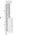
- FIG. 1 is a schematic plan view showing a biomedical electrode according to a first embodiment of the present invention.
- FIG. 2 is a schematic cross-sectional view taken along the line II-II in FIG.
- FIG. 3 is a schematic plan view showing a biological electrode according to the second embodiment of the present invention.
- 4 is a schematic cross-sectional view taken along line IV-IV in FIG.
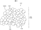
- FIG. 5 is a schematic diagram showing an example of a schematic particle structure of silica made of gelled silica.
- FIG. 6 is a schematic diagram schematically showing an example of a particle structure of silver chloride-supporting silica in which silver chloride is supported on silica made of gelled silica.
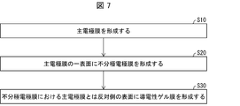
- FIG. 7 is a flowchart illustrating a method for forming a biomedical electrode.
- FIG. 1 is a schematic plan view showing a biomedical electrode according to a first embodiment of the present invention.
- FIG. 2 is a schematic cross-sectional view taken along the line II-II in FIG.
- the bioelectrode 1 includes a protective film 2, a main electrode film 3, an unpolarized electrode film 4, a conductive gel film 5, a release film 6, a lead wire 7, and a lead wire protective film 8. Yes.
- the protective film 2 includes a rectangular electrode protection portion 2A in plan view and a lead wire protection portion extending in one direction (right direction in FIG. 1) from the central portion of one side (right side in FIG. 1) of the electrode protection portion 2A. 2B.
- the protective film 2 includes a nonwoven fabric 21 and a resin film 22 formed on one surface (lower surface in FIG. 2) of the nonwoven fabric 81.
- the resin film 22 is made of polyethylene (PE).
- the main electrode film 3 has substantially the same planar shape as the protective film 2.
- the main electrode film 3 includes a base material 31 and a metal film 32 formed on one surface (the lower surface in FIG. 2) of the base material 31.
- the base material 31 is made of polyethylene terephthalate (PET)
- the metal film 32 is made of a silver vapor deposition film.
- Such a silver vapor deposition film can be formed by vapor-depositing silver on one surface of the substrate 31.
- the main electrode film 3 is bonded to one surface (lower surface in FIG. 2) of the protective film 2 with the surface (upper surface in FIG. 2) facing the base material 31 facing.
- the non-polarized electrode film 4 is formed on the surface of the main electrode film 3 opposite to the protective film 2 (the surface on the metal film 32 side) and in a region facing the electrode protection portion 2A of the protective film 2. .
- the non-polarized electrode film 4 is composed of an electrode film including a silver chloride carrier comprising a carrier and silver chloride carried on the carrier.
- Such an electrode film (unpolarized electrode film 4) can be formed from a silver chloride paste containing a silver chloride carrier. Details of the silver chloride paste containing the silver chloride carrier will be described later.
- the conductive gel film 5 is formed on almost the entire surface of the non-polarized electrode film 4 opposite to the main electrode film 3.
- the conductive gel film 5 is a part that directly contacts the skin of the living body when the bioelectrode 1 is used.
- the release film 6 is formed on almost the entire surface of the non-polarized electrode film 4 opposite to the main electrode film 3.
- the release film 6 is a release paper (release paper), a fluorine film, a polyethylene naphthalate (PEN) film in which a silicone or non-silicone (melamine, acrylic, etc.) release agent is applied on one or both sides, polyethylene A terephthalate (PET) film or the like is used.
- the release film 6 is peeled off when the biological electrode 1 is used.
- the lead wire 7 includes a strip-like base material 71 having a narrower width than the lead wire protection portion 2B of the protective film 2 in plan view, and a metal film 72 formed on one surface (upper surface in FIG. 2) of the base material 71. It consists of.
- the base material 71 is made of PET
- the metal film 72 is made of a silver vapor deposition film. Such a silver vapor deposition film can be formed by vapor-depositing silver on one surface of the substrate 71.
- the lead wire 7 is a surface of the main electrode film 3 opposite to the protective film 2 (the surface on the metal film 32 side, the lower surface in FIG. 2), and is in a region corresponding to the lead wire protection part 2B of the protective film 2. The bonding is performed with the metal film 72 side facing each other. The end of the lead wire 7 on the side of the electrode protection part 2A does not reach the electrode protection part 2A in a plan view and does not contact the non-polarized electrode film 4.
- the lead wire protective film 8 has substantially the same planar shape as the lead wire protective part 2B in the protective film 2.
- the lead wire protective film 8 includes a nonwoven fabric 81 and a resin film 82 formed on one surface of the nonwoven fabric 81 (upper surface in FIG. 2).
- the resin film 82 is made of PE.
- the lead wire protective film 8 is the surface of the main electrode film 3 opposite to the protective film 2 side (the surface on the metal film 32 side, the lower surface in FIG. 2), and corresponds to the lead wire protection part 2B of the protective film 2 In a state where the surface on the resin film 82 side is opposed to the region to be covered, the lead wire 7 is covered. Thereby, the lead wire 7 is covered with the protective film 2 mainly covering the upper surface of the lead wire 7 and the lead wire protective film 8 mainly covering the lower surface of the lead wire.
- the aforementioned living body electrode 1 is manufactured as follows, for example.
- An elongated rectangular protective film forming member (a member for forming the protective film 2) is prepared which is long in one direction in plan view and has a width equal to the width of the electrode protective portion 2A described above.
- an elongated rectangular lead wire protective film forming member (member for forming the lead wire protective film 8) having a long plan view in one direction and a width substantially equal to the width of the protective film forming member is prepared.
- a rectangular main electrode film forming member (a member for forming the main electrode film 3) having a rectangular shape in plan view and a width substantially equal to the width of the electrode protection portion 2A is prepared.
- the non-polarized electrode film 4 is formed on one end portion of the main electrode film forming member (the surface on the metal film side, the lower surface in FIG. 2) (the region corresponding to the electrode protection portion 2A of the protection film 2).
- a formed laminated electrode film is prepared.
- This laminated electrode film is, for example, formed in a silver chloride paste containing a silver chloride carrier on one end (surface on the metal film side) of one surface of the main electrode film forming member, and then included in the silver chloride paste. Produced by drying the solvent.
- the silver chloride paste can be formed on the main electrode film forming member by printing, transferring, coating, or the like.
- the solvent drying is performed by, for example, heat treatment at 110 ° C. for 3 minutes to 5 minutes.
- the thickness of the non-polarized electrode film 4 is, for example, an arbitrary thickness within the range of 1 ⁇ m to 100 ⁇ m, for example, 20 ⁇ m.
- membrane 5 was formed in one surface (FIG. 2 upper surface) of the peeling film 6 is prepared. Furthermore, a lead wire 7 is prepared. First, the laminated electrode film is bonded to one surface (the lower surface in FIG. 2) of the protective film forming member with the surface on the main electrode film forming member side facing. Next, a gel sheet with a release film is bonded to the surface of the laminated electrode film on the side of the nonpolarizing electrode film 4 with the surface on the side of the conductive gel film 5 facing.
- the lead wire 7 is placed on the surface of the main electrode film forming member opposite to the protective film forming member and in the region facing the lead wire protection portion planned region in the protective film forming member. Bonding is performed with the surface on the film 72 side (the upper surface in FIG. 2) facing each other.
- the lead wire is placed on the surface of the main electrode film forming member on the side to which the lead wire is bonded (the lower surface in FIG. 2) and in the region facing the lead wire protection portion planned region in the protective film forming member.
- the protective film forming member is bonded so as to cover the lead wire 7 with the surface on the resin film 82 side facing each other.
- the protective film forming member, the main electrode film forming member, and the lead wire protective film forming member are patterned so as to have the shapes of the protective film 2, the main electrode film 3, and the lead wire protective film 8, respectively.
- the biological electrode 1 shown in FIGS. 1 and 2 is obtained.
- the non-polarized electrode film 4 is composed of an electrode film including a silver chloride carrier composed of a carrier and silver chloride carried on the carrier. Therefore, when an unpolarized electrode film whose total amount of exposed area of silver chloride in the unpolarized electrode film 4 is a predetermined amount is obtained, the unpolarized electrode film containing silver / silver chloride described in Patent Document 1 As compared with the above, the total amount of silver can be reduced. Thereby, it is possible to reduce the cost while maintaining the nonpolarization property.
- the main electrode film 3 is composed of the base material 31 and the metal film 32 formed on one surface (the lower surface in FIG. 2) of the base material 31.
- membrane 3 may be comprised only from metal films, such as silver.
- the metal film 32 is composed of a silver vapor deposition film, but the metal film 32 may be a metal vapor deposition film other than silver.
- the metal film 32 may be a metal sputtered film formed by a sputtering method or a metal plated film formed by a plating method.
- FIG. 3 is a schematic plan view showing a biological electrode according to a second embodiment of the present invention. 4 is a schematic cross-sectional view taken along the line IV-IV in FIG.
- the biological electrode 1A according to the second embodiment is similar to the biological electrode 1 according to the first embodiment described above, and includes a protective film 2, a main electrode film 3A, an unpolarized electrode film 4, and a conductive material.
- the gel film 5, the release film 6, the lead wire 7, and the lead wire protective film 8 are included.
- the shape and the configuration of the protective film 2, the non-polarized electrode film 4, the conductive gel film 5, the release film 6, the lead wire 7 and the lead wire protective film 8 in the biological electrode 1A according to the second embodiment are respectively first.
- the shape and configuration of the protective film 2, the non-polarized electrode film 4, the conductive gel film 5, the release film 6, the lead wire 7, and the lead wire protective film 8 according to the embodiment are the same.
- the biological electrode 1A according to the second embodiment differs from the biological electrode 1 according to the first embodiment described above in the structure for attaching the lead wire 7 and the shape and material of the main electrode film 3A. ing.
- the main electrode film 3A has the same planar shape as the electrode protection part 2A of the protective film 2.
- the main electrode film 3 is composed of an electrode film containing silver.
- Such an electrode film can be formed from, for example, a silver paste (silver ink).
- the lead wire 7 is bonded to the surface of the protective film 2 on the resin film 22 side (the lower surface in FIG. 4) with the surface of the base material 71 facing the surface.
- the lead wires 7 are arranged so as to pass through the width central portion of the surface of the lead wire protection portion 2B of the protective film 2 on the resin film 22 side in plan view, but the electrode protection portion 2A of the lead wire 7 is disposed. One end portion on the side is disposed on the electrode protection portion 2A side beyond the lead wire protection portion 2B of the protective film 2.
- the nonpolarizing electrode film 4 is formed so as to cover one end of the lead wire 7 on almost the entire surface of the main electrode film 3A opposite to the protective film 2 (the lower surface in FIG. 4).
- the conductive gel film 5 is formed on almost the entire surface of the non-polarized electrode film 4 opposite to the main electrode film 3A.
- the release film 6 is formed on almost the entire surface of the non-polarized electrode film 4 opposite to the main electrode film 3A.
- the lead wire protective film 8 covers the lead wire 7 with the surface on the resin film 82 side facing the surface (the lower surface in FIG. 4) of the protective film 2 on which the lead wire 7 is formed. It is joined to. Thereby, the lead wire 7 is covered with the protective film 2 mainly covering the upper surface of the lead wire 7 and the lead wire protective film 8 mainly covering the lower surface of the lead wire.
- the biological electrode 1A described above is manufactured, for example, as follows.
- An elongated rectangular protective film forming member (a member for forming the protective film 2) is prepared which is long in one direction in plan view and has a width equal to the width of the electrode protective portion 2A described above.
- an elongated rectangular lead wire protective film forming member (a member for forming the lead wire protective film 8) having a long plan view in one direction and a width equal to the width of the protective film forming member is prepared.
- a laminated electrode film holding film in which a laminated film (laminated electrode film) of the main electrode film 3A and the non-polarized electrode film 4 is prepared on a polyester (PET) film substrate (not shown) is prepared.
- This laminated electrode film holding film is manufactured as follows, for example. That is, first, after forming a silver paste on a release film (not shown), the silver paste is dried to form the main electrode film 3A on the polyester film substrate. Then, after forming a silver chloride paste containing a silver chloride carrier on the surface of the main electrode film 3A, the silver chloride paste is dried to form the nonpolarized electrode film 4 on the main electrode film 3A. In this way, a laminated electrode film holding film is obtained.
- the thickness of the non-polarized electrode film 4 is, for example, an arbitrary thickness within the range of 1 ⁇ m to 100 ⁇ m, for example, 20 ⁇ m.
- the gel sheet with a peeling film in which the electroconductive gel film 5 was formed in one surface (upper surface in FIG. 4) of the peeling film 6 is prepared. Furthermore, a lead wire 7 is prepared. First, the lead wire 7 is bonded to one surface (the lower surface in FIG. 4) of the protective film forming member in a state where the surface on the substrate 71 side is opposed to the surface. At this time, most of the lead wire 7 passes through the width central portion of the surface of the lead wire protection portion 2B of the protection film 2 on the resin film 22 side, and one end portion of the lead wire 7 on the electrode protection portion 2A side is the lead wire protection portion. The lead wire 7 is disposed so as to protrude beyond 2B to the electrode protection portion 2A side.
- the polyester film substrate is peeled from the laminated electrode film holding film to obtain a laminated electrode film composed of the main electrode film 3A and the nonpolarized electrode film 4. Then, on one surface (the lower surface in FIG. 4) of the protective film forming member, the laminated electrode film is placed in a region corresponding to the electrode protection portion 2A, with the surface on the main electrode film 3A side facing. Then, bonding is performed so as to cover one end of the lead wire 7. Next, a gel sheet with a release film is bonded to the surface of the laminated electrode film on the side of the nonpolarizing electrode film 4 with the surface on the side of the conductive gel film 5 facing.
- the lead wire protective film is formed in a region facing the planned lead wire protection portion region in the protective film forming member.
- the forming member is joined so as to cover the lead wire 7 with the surface on the resin film 82 side facing each other.
- the protective film forming member and the lead wire protective film forming member are patterned so as to have the shapes of the protective film 2 and the lead wire protective film 8, respectively. Thereby, the biological electrode 1A shown in FIGS. 3 and 4 is obtained.
- the non-polarized electrode film 4 is composed of an electrode film including a silver chloride carrier composed of a carrier and silver chloride carried on the carrier. Therefore, when an unpolarized electrode film whose total amount of exposed area of silver chloride in the unpolarized electrode film 4 is a predetermined amount is obtained, the unpolarized electrode film containing silver / silver chloride described in Patent Document 1 As compared with the above, the total amount of silver can be reduced. Thereby, it is possible to reduce the cost while maintaining the nonpolarization property.
- the main electrode film 3 is made of an electrode film containing silver, but may be made of an electrode film containing carbon. Such an electrode film can be formed from a carbon paste.
- the main electrode film 3 may be formed from a conductive paste other than silver paste and carbon paste.
- Silver chloride paste for forming unpolarized electrode film is a silver chloride formed by supporting a binder resin and silver chloride on a carrier. A carrier. Since such a silver chloride paste contains a silver chloride carrier, it has nonpolarization properties.
- Binder Resin As the binder resin, for example, a thermoplastic resin can be used.
- polyester resin polyurethane resin, acrylic resin, alkyd resin, phenoxy resin, butyral resin, polyvinyl alcohol resin, or the like can be used as the binder resin.
- polyester resin include solvent-soluble polyesters TP-220, TP-217, TP-249, TP-235, TP-236, TP-290, TP-270, LP-manufactured by Nippon Synthetic Chemical Co., Ltd.
- the silver chloride carrier comprises a carrier and silver chloride carried on the carrier.
- Carrier As the material for the carrier, various materials such as metal (preferably a metal other than silver), nonmetal, organic matter, or inorganic matter can be used. In order to facilitate the dispersion of the silver chloride support in the binder resin, it is preferable not to precipitate the silver chloride support in the binder resin.
- the carrier preferably has a density close to that of the binder resin. Further, the carrier is more preferably a low-cost one that can easily carry silver chloride.
- the carrier includes (1) acrylic resin, polyurethane resin, polyester resin, or polyamide resin, (2) polymer particles made of epoxy resin, silica, mica, or glass beads, (3) calcium carbonate, etc. Inorganic particles consisting of can be used.
- Example 1 of silver chloride carrier is silver chloride-supported silica in which silver chloride is supported on silica (silicon dioxide).
- the silica on which silver chloride is supported may be wet method silica such as precipitation method silica or gelation method silica (gel method silica), or may be dry method silica.
- the silica is preferably gelled silica.
- the silica is gelled silica.
- FIG. 5 is a schematic diagram showing an example of a schematic particle structure of silica made of gelled silica.
- Silica 102 made of gelled silica has a particle structure in which, for example, a plurality of primary particles (skeleton particles) 103A gather in the shape of a bunch of grapes to form secondary particles 103.
- the specific surface area of silica refers to the surface area per unit mass.
- the surface area of silica is the sum of the external area and internal area of silica (the area of the pore inner surface of silica).
- the pore volume of silica refers to the volume of silica pores per unit mass.
- the average pore diameter of silica refers to the average diameter of silica pores (voids).
- the average particle diameter of silica refers to the average of the diameters D (see FIG. 5) of the secondary particles.
- the specific surface area of silica is preferably 20 m 2 / g or more and 1000 m 2 / g or less, and particularly preferably 100 m 2 / g or more and 700 m 2 / g or less.
- the pore volume of silica is preferably 0.2 ml / g or more and 2.0 ml / g or less, and particularly preferably 0.3 ml / g or more and 1.2 ml / g or less.
- the average pore diameter of silica is preferably 2 nm or more and 100 nm or less, and particularly preferably 2 nm or more and 30 nm or less.
- the average particle diameter of silica is preferably 1 ⁇ m or more and 50 ⁇ m or less, and particularly preferably 2 ⁇ m or more and 30 ⁇ m or less.
- FIG. 6 is a schematic diagram schematically showing an example of a particle structure of silver chloride-supporting silica in which silver chloride is supported on silica made of gelled silica.
- the silver chloride-supporting silica 101 shown in FIG. 6 includes silica 102 and silver chloride 104 supported on the surface of the silica 102 (including the content surface of the pores).
- the silver chloride-supporting silica is produced by the following production method. This manufacturing method includes the steps of generating a silver compound solution by dissolving the silver compound in the solution, and supporting the silver compound on silica (including the inner surface of the pores) using the silver compound solution. .
- As the silver compound silver nitrate or silver chloride is used.
- silver nitrate when silver nitrate is used as the silver compound, first, a silver nitrate solution is generated by dissolving silver nitrate powder in an aqueous solvent. Next, silver nitrate is supported on silica using a silver nitrate solution. Examples of the method for supporting silver nitrate on silica include a precipitation method, a gelation method, an impregnation method, and an ion exchange method. After that, silver chloride is supported on silica by reacting silver nitrate supported on silica with a compound containing chloride ions such as hydrochloric acid or sodium chloride.
- silver chloride when silver chloride is used as the silver compound, first, silver chloride powder is dissolved in an aqueous solution such as ammonia water, concentrated hydrochloric acid solution, alkaline cyanide aqueous solution, thiosulfate aqueous solution, or ammonium carbonate aqueous solution. To produce a silver chloride solution. Next, silver chloride is supported on silica using a silver chloride solution. Examples of the method for supporting silver chloride on silica include a precipitation method, a gelation method, an impregnation method, and an ion exchange method.
- an aqueous solution such as ammonia water, concentrated hydrochloric acid solution, alkaline cyanide aqueous solution, thiosulfate aqueous solution, or ammonium carbonate aqueous solution.
- an aqueous solution such as ammonia water, concentrated hydrochloric acid solution, alkaline cyanide aqueous solution, thiosulfate
- Example 1 of silver chloride-supported silica contains silica (Silicia 710 (trade name) manufactured by Fuji Silysia Chemical Co., Ltd.) that is a gelled silica and silver chloride (AgCl) supported on the silica.
- the content of silica (silicon dioxide) is 61% by weight and the silver chloride content is 39% by weight.
- the specific surface area of silica is 397 m 2 / g, and the average particle diameter of silica is 2.9 ⁇ m.
- Example 1 of silver chloride-supporting silica A method for producing Example 1 of silver chloride-supporting silica will be described.
- a silver nitrate solution was prepared by dissolving 40 g of silver nitrate powder with 50 ml of ion-exchanged water.
- 20 g of silica (Silicia 710 (trade name), manufactured by Fuji Silysia Chemical Ltd.) was added to the silver nitrate solution and stirred for 4 hours.
- the solid content was recovered from the stirred solution using 5 types A filter paper, and the recovered solid content was dried with a shelf dryer at 120 ° C. for 16 hours.
- silver nitrate-supporting silica in which silver nitrate was supported on silica was obtained.
- Another method for producing a silver chloride carrier The silver chloride carrier can also be produced by coating a carrier with silver and then subjecting it to a chlorination treatment.
- a method for coating the carrier with silver methods described in Patent Documents 2 and 3 can be used.
- Example of Method for Producing Silver Chloride Paste An example of a method for producing a silver chloride paste when the silver chloride carrier is silver chloride-supported silica will be described.
- 50 g of silver chloride-supporting silica powder was put in a container with a lid.
- the amount of silver chloride supported on the silver chloride-supported silica is an arbitrary amount within the range of 0.1 wt% to 80 wt%.
- 25 g of a mixed solvent of MEK (methyl ethyl ketone), ethyl acetate and toluene (mixing ratio 1: 1: 1) was put into the container and mixed with the silver chloride-supporting silica powder.
- 50 g of a binder resin solvent soluble type polyester LP-035 (solid content: 40%) manufactured by Nippon Synthetic Chemical Co., Ltd.
- stirring was performed for 10 minutes at a rotation speed of 3500 r / min. Thereby, the fluid silver chloride paste without powder aggregation was obtained.
- -Silver chloride has the property of being easy to aggregate (low dispersibility), while silica is hard to aggregate (high dispersibility). For this reason, silver chloride-supporting silica has higher dispersibility than silver chloride and is less likely to aggregate. Thereby, in a silver chloride paste using silver chloride-supporting silica, silver chloride (silver chloride-supporting silica) is less likely to aggregate. In the silver chloride-supporting silica, silver chloride is supported on silica (including the inner surface of the pores).
- the silver chloride paste using the silver chloride-supporting silica is compared with the conventional silver / silver chloride paste.
- the surface area of silver chloride can be increased.
- the polarization suppression effect can be improved.
- silver chloride-supporting silica silver chloride is supported on silica (including the inner surface of the pores).
- the main electrode film has a base material and a metal film formed on one surface of the base material.
- the biological electrode according to aspect 3 of the invention is the above-described aspect 1, wherein the main electrode film is made of a metal film.
- the biological electrode according to aspect 4 of the invention is the above-described aspect 2 or 3, wherein the metal film is one arbitrarily selected from a metal vapor deposition film, a metal sputtered film, and a metal plating film.
- the metal film is made of silver.
- the biological electrode according to aspect 6 of the present invention is the above-described aspect 1, wherein the main electrode film is composed of an electrode film containing silver or an electrode film containing carbon.
- a biological electrode according to aspect 7 of the invention further includes a protective film formed on the surface of the main electrode film opposite to the non-polarized electrode film in any of the above aspects 1 to 6.
- the biological electrode according to Aspect 8 of the invention further includes a release film formed on the surface of the conductive gel film opposite to the non-polarized electrode film in any one of Aspects 1 to 7.
- the carrier is silica.
- a biological electrode according to aspect 10 of the present invention further includes a lead wire having one end electrically connected to the main electrode film in any of the above aspects 1 to 9.
- a biological electrode according to an eleventh aspect of the invention includes, in order, a main electrode film, an unpolarized electrode film, and a conductive gel film, and the unpolarized electrode film includes a carrier and silver chloride supported on the carrier. It is comprised from the electrode film containing the silver chloride support body which has this.
- the biological electrode forming method according to the twelfth aspect of the present invention includes a step of forming a main electrode film (S10), a step of forming an unpolarized electrode film on one surface of the main electrode film (S20), and the non-polarization.
- the electrode film includes a silver chloride carrier having silver chloride.
- the biological electrode forming method according to the thirteenth aspect of the invention includes a step of forming a main electrode film (S10), a step of forming a conductive gel film on one surface of the main electrode film (S20), and the conductive Forming an unpolarized electrode film on the surface of the gel film opposite to the side on which the main electrode film is formed (S30), and the unpolarized electrode film is supported on the carrier and the carrier
- the electrode film includes a silver chloride carrier having silver chloride.
Abstract
This bioelectrode (1) comprises: a main electrode film (3); a non-polarizable electrode film (4) formed on one surface of the main electrode film (3); and a conductive gel film (5) formed on a surface of the non-polarizable electrode film (4) situated on the opposite side of the main electrode film. The non-polarizable electrode film (4) comprises an electrode film that includes a silver chloride support having a carrier and silver chloride supported thereby.
Description
この発明は、生体用電極、及び生体用電極の形成方法に関する。
The present invention relates to a biological electrode and a method for forming a biological electrode.
特許文献1には、銀/塩化銀を含む不分極電極膜を備えた生体用電極が開示されている。
Patent Document 1 discloses a biological electrode provided with an unpolarized electrode film containing silver / silver chloride.
特許文献1の生体用電極は、銀/塩化銀を含む不分極電極膜を備えている。不分極電極膜に含まれる銀は高価なため、特許文献1の生体用電極では、コストが高くなるという問題がある。
この発明は、不分極性を維持したまま、低廉化が図れる生体用電極を提供することを目的とする。 The living body electrode of Patent Document 1 includes an unpolarized electrode film containing silver / silver chloride. Since silver contained in the non-polarized electrode film is expensive, the living body electrode of Patent Document 1 has a problem of high cost.
It is an object of the present invention to provide a biological electrode that can be made inexpensive while maintaining nonpolarity.
上記目的を達成するための発明の態様1に係る発明は、主電極膜と、前記主電極膜の一表面に形成された不分極電極膜と、前記不分極電極膜における前記主電極膜とは反対側の表面に形成された導電性ゲル膜とを含み、前記不分極電極膜は、担体と前記担体に担持された塩化銀を有する塩化銀担持体を含む電極膜から構成されている、生体用電極である。
この構成では、不分極電極膜は、担体と前記担体に担持された塩化銀を有する塩化銀担持体を含む電極膜から構成されているので、不分極電極膜内での塩化銀の露出面積の総量が所定量である不分極電極膜を得ようとした場合に、特許文献1に記載の銀/塩化銀を含む不分極電極膜に比べて、銀の総量を低減させることができる。これにより、不分極性を維持したまま、低廉化が図れる。 The invention according to aspect 1 of the invention for achieving the above object is characterized in that the main electrode film, the unpolarized electrode film formed on one surface of the main electrode film, and the main electrode film in the unpolarized electrode film are: A living body comprising an electroconductive gel film formed on the opposite surface, wherein the non-polarized electrode film comprises an electrode film comprising a carrier and a silver chloride carrier having silver chloride carried on the carrier. Electrode.
In this configuration, the non-polarized electrode film is composed of an electrode film including a carrier and a silver chloride carrier having silver chloride supported on the carrier, so that the exposed area of silver chloride in the non-polarized electrode film is reduced. When an unpolarized electrode film whose total amount is a predetermined amount is to be obtained, the total amount of silver can be reduced as compared with the nonpolarized electrode film containing silver / silver chloride described in Patent Document 1. Thereby, it is possible to reduce the cost while maintaining the nonpolarization property.
以下では、この発明の実施形態を、添付図面を参照して説明する。
[1]第1の実施形態
図1は、本発明の第1の実施形態に係る生体用電極を示す図解的な平面図である。図2は、図1のII-II線に沿う図解的な断面図である。
生体用電極1は、保護膜2と、主電極膜3と、不分極電極膜4と、導電性ゲル膜5と、剥離フィルム6と、リード線7と、リード線保護膜8とを含んでいる。 Hereinafter, embodiments of the present invention will be described with reference to the accompanying drawings.
[1] First Embodiment FIG. 1 is a schematic plan view showing a biomedical electrode according to a first embodiment of the present invention. FIG. 2 is a schematic cross-sectional view taken along the line II-II in FIG.
The bioelectrode 1 includes aprotective film 2, a main electrode film 3, an unpolarized electrode film 4, a conductive gel film 5, a release film 6, a lead wire 7, and a lead wire protective film 8. Yes.
[1]第1の実施形態
図1は、本発明の第1の実施形態に係る生体用電極を示す図解的な平面図である。図2は、図1のII-II線に沿う図解的な断面図である。
生体用電極1は、保護膜2と、主電極膜3と、不分極電極膜4と、導電性ゲル膜5と、剥離フィルム6と、リード線7と、リード線保護膜8とを含んでいる。 Hereinafter, embodiments of the present invention will be described with reference to the accompanying drawings.
[1] First Embodiment FIG. 1 is a schematic plan view showing a biomedical electrode according to a first embodiment of the present invention. FIG. 2 is a schematic cross-sectional view taken along the line II-II in FIG.
The bioelectrode 1 includes a
保護膜2は、平面視で矩形状の電極保護部2Aと、電極保護部2Aの1辺(図1では右辺)の中央部から一方向(図1では右方向)に延びたリード線保護部2Bとを備えている。この実施形態では、保護膜2は、不織布21と、不織布81の一方の表面(図2では下面)に形成された樹脂膜22とからなる。この実施形態では、樹脂膜22は、ポリエチレン(PE)からなる。
The protective film 2 includes a rectangular electrode protection portion 2A in plan view and a lead wire protection portion extending in one direction (right direction in FIG. 1) from the central portion of one side (right side in FIG. 1) of the electrode protection portion 2A. 2B. In this embodiment, the protective film 2 includes a nonwoven fabric 21 and a resin film 22 formed on one surface (lower surface in FIG. 2) of the nonwoven fabric 81. In this embodiment, the resin film 22 is made of polyethylene (PE).
主電極膜3は、保護膜2とほぼ同じ平面形状を有している。この実施形態では、主電極膜3は、基材31と、基材31の一方の表面(図2では下面)に形成された金属膜32とからなる。この実施形態では、基材31はポリエチレンテレフタレート(PET)からなり、金属膜32は銀蒸着膜からなる。このような銀蒸着膜は、基材31の一方の表面に銀を蒸着することによって形成できる。主電極膜3は、保護膜2の一方の表面(図2では下面)に、その基材31側の表面(図2では上面)が対向した状態で、接合されている。
The main electrode film 3 has substantially the same planar shape as the protective film 2. In this embodiment, the main electrode film 3 includes a base material 31 and a metal film 32 formed on one surface (the lower surface in FIG. 2) of the base material 31. In this embodiment, the base material 31 is made of polyethylene terephthalate (PET), and the metal film 32 is made of a silver vapor deposition film. Such a silver vapor deposition film can be formed by vapor-depositing silver on one surface of the substrate 31. The main electrode film 3 is bonded to one surface (lower surface in FIG. 2) of the protective film 2 with the surface (upper surface in FIG. 2) facing the base material 31 facing.
不分極電極膜4は、主電極膜3における保護膜2とは反対側の表面(金属膜32側の表面)であって、保護膜2の電極保護部2Aに対向する領域に形成されている。不分極電極膜4は、担体と担体に担持された塩化銀とからなる塩化銀担持体を含む電極膜から構成されている。このような電極膜(不分極電極膜4)は、塩化銀担持体を含む塩化銀ペーストから形成することができる。塩化銀担持体を含む塩化銀ペーストの詳細については後述する。
The non-polarized electrode film 4 is formed on the surface of the main electrode film 3 opposite to the protective film 2 (the surface on the metal film 32 side) and in a region facing the electrode protection portion 2A of the protective film 2. . The non-polarized electrode film 4 is composed of an electrode film including a silver chloride carrier comprising a carrier and silver chloride carried on the carrier. Such an electrode film (unpolarized electrode film 4) can be formed from a silver chloride paste containing a silver chloride carrier. Details of the silver chloride paste containing the silver chloride carrier will be described later.
導電性ゲル膜5は、不分極電極膜4における主電極膜3とは反対側の表面のほぼ全面に形成されている。導電性ゲル膜5は、生体用電極1の使用時には、生体の皮膚に直接的に接触する部分である。導電性ゲル膜5としては、例えば、積水化学工業株式会社製のハイドロゲル HIT-B3R,CR-H,CR-RA等を使用できる。
剥離フィルム6は、不分極電極膜4における主電極膜3とは反対側の表面のほぼ全面に形成されている。剥離フィルム6としては、剥離紙(離型紙)、フッ素フィルム、片面または両面にシリコーン系または非シリコーン系(メラミン系、アクリル系等)の離型剤を塗布したポリエチレンナフタレート(PEN)フィルム、ポリエチレンテレフタレート(PET)フィルム等が用いられる。剥離フィルム6は、生体用電極1を使用する際には、剥がされる。 Theconductive gel film 5 is formed on almost the entire surface of the non-polarized electrode film 4 opposite to the main electrode film 3. The conductive gel film 5 is a part that directly contacts the skin of the living body when the bioelectrode 1 is used. As the conductive gel film 5, for example, hydrogel HIT-B3R, CR-H, CR-RA manufactured by Sekisui Chemical Co., Ltd. can be used.
Therelease film 6 is formed on almost the entire surface of the non-polarized electrode film 4 opposite to the main electrode film 3. The release film 6 is a release paper (release paper), a fluorine film, a polyethylene naphthalate (PEN) film in which a silicone or non-silicone (melamine, acrylic, etc.) release agent is applied on one or both sides, polyethylene A terephthalate (PET) film or the like is used. The release film 6 is peeled off when the biological electrode 1 is used.
剥離フィルム6は、不分極電極膜4における主電極膜3とは反対側の表面のほぼ全面に形成されている。剥離フィルム6としては、剥離紙(離型紙)、フッ素フィルム、片面または両面にシリコーン系または非シリコーン系(メラミン系、アクリル系等)の離型剤を塗布したポリエチレンナフタレート(PEN)フィルム、ポリエチレンテレフタレート(PET)フィルム等が用いられる。剥離フィルム6は、生体用電極1を使用する際には、剥がされる。 The
The
リード線7は、平面視で保護膜2のリード線保護部2Bよりも幅が狭い帯状の基材71と、当該基材71の一方の表面(図2では上面)に形成された金属膜72とからなる。この実施形態では、基材71はPETからなり、金属膜72は銀蒸着膜からなる。このような銀蒸着膜は、基材71の一方の表面に銀を蒸着することに形成できる。リード線7は、主電極膜3における保護膜2とは反対側の面(金属膜32側の面、図2では下面)であって、保護膜2のリード線保護部2Bに対応する領域に、その金属膜72側の表面を対向させた状態で接合されている。リード線7の電極保護部2A側端は、平面視で電極保護部2Aに達しておらず、不分極電極膜4に接していない。
The lead wire 7 includes a strip-like base material 71 having a narrower width than the lead wire protection portion 2B of the protective film 2 in plan view, and a metal film 72 formed on one surface (upper surface in FIG. 2) of the base material 71. It consists of. In this embodiment, the base material 71 is made of PET, and the metal film 72 is made of a silver vapor deposition film. Such a silver vapor deposition film can be formed by vapor-depositing silver on one surface of the substrate 71. The lead wire 7 is a surface of the main electrode film 3 opposite to the protective film 2 (the surface on the metal film 32 side, the lower surface in FIG. 2), and is in a region corresponding to the lead wire protection part 2B of the protective film 2. The bonding is performed with the metal film 72 side facing each other. The end of the lead wire 7 on the side of the electrode protection part 2A does not reach the electrode protection part 2A in a plan view and does not contact the non-polarized electrode film 4.
リード線保護膜8は、保護膜2におけるリード線保護部2Bとほぼ同じ平面形状を有している。この実施形態では、リード線保護膜8は、不織布81と、不織布81の一方の表面(図2では上面)に形成された樹脂膜82とからなる。この実施形態では、樹脂膜82は、PEからなる。リード線保護膜8は、主電極膜3における保護膜2側とは反対側の面(金属膜32側の面、図2では下面)であって、保護膜2のリード線保護部2Bに対応する領域に、その樹脂膜82側の表面を対向させた状態で、リード線7を覆うように接合されている。これにより、リード線7は、主としてリード線7の上面を覆う保護膜2と、主としてリード線の下面を覆うリード線保護膜8とによって被覆される。
The lead wire protective film 8 has substantially the same planar shape as the lead wire protective part 2B in the protective film 2. In this embodiment, the lead wire protective film 8 includes a nonwoven fabric 81 and a resin film 82 formed on one surface of the nonwoven fabric 81 (upper surface in FIG. 2). In this embodiment, the resin film 82 is made of PE. The lead wire protective film 8 is the surface of the main electrode film 3 opposite to the protective film 2 side (the surface on the metal film 32 side, the lower surface in FIG. 2), and corresponds to the lead wire protection part 2B of the protective film 2 In a state where the surface on the resin film 82 side is opposed to the region to be covered, the lead wire 7 is covered. Thereby, the lead wire 7 is covered with the protective film 2 mainly covering the upper surface of the lead wire 7 and the lead wire protective film 8 mainly covering the lower surface of the lead wire.
前述の生体用電極1は、例えば、次のように製造される。
平面視が一方向に長くかつ幅が前述した電極保護部2Aの幅と等しい細長矩形の保護膜形成用部材(保護膜2を形成するための部材)を用意する。また、平面視が一方向に長くかつ幅が保護膜形成用部材の幅とほぼ等しい細長矩形のリード線保護膜形成用部材(リード線保護膜8を形成するための部材)を用意する。 The aforementioned living body electrode 1 is manufactured as follows, for example.
An elongated rectangular protective film forming member (a member for forming the protective film 2) is prepared which is long in one direction in plan view and has a width equal to the width of the electrodeprotective portion 2A described above. In addition, an elongated rectangular lead wire protective film forming member (member for forming the lead wire protective film 8) having a long plan view in one direction and a width substantially equal to the width of the protective film forming member is prepared.
平面視が一方向に長くかつ幅が前述した電極保護部2Aの幅と等しい細長矩形の保護膜形成用部材(保護膜2を形成するための部材)を用意する。また、平面視が一方向に長くかつ幅が保護膜形成用部材の幅とほぼ等しい細長矩形のリード線保護膜形成用部材(リード線保護膜8を形成するための部材)を用意する。 The aforementioned living body electrode 1 is manufactured as follows, for example.
An elongated rectangular protective film forming member (a member for forming the protective film 2) is prepared which is long in one direction in plan view and has a width equal to the width of the electrode
また、平面視が一方向に長くかつ幅が前述の電極保護部2Aの幅とほぼ等しい矩形の主電極膜形成用部材(主電極膜3を形成するための部材)を用意する。そして、この主電極膜形成用部材の一方の表面(金属膜側の表面、図2では下面)の一端部(保護膜2の電極保護部2Aに対応する領域)に、不分極電極膜4が形成された積層電極膜を用意する。この積層電極膜は、例えば、主電極膜形成用部材の一方の表面(金属膜側の表面)の一端部に、塩化銀担持体を含む塩化銀ペーストを形成した後、当該塩化銀ペーストに含まれる溶剤を乾燥させることにより製造される。主電極膜形成用部材への塩化銀ペーストの形成は、印刷、転写、又は塗布等によって行うことができる。また、溶剤乾燥は、例えば、110℃で3分~5分の熱処理によって行われる。不分極電極膜4の厚さは、例えば1μm~100μmの範囲内の任意の厚さであり、例えば20μmである。
Further, a rectangular main electrode film forming member (a member for forming the main electrode film 3) having a rectangular shape in plan view and a width substantially equal to the width of the electrode protection portion 2A is prepared. Then, the non-polarized electrode film 4 is formed on one end portion of the main electrode film forming member (the surface on the metal film side, the lower surface in FIG. 2) (the region corresponding to the electrode protection portion 2A of the protection film 2). A formed laminated electrode film is prepared. This laminated electrode film is, for example, formed in a silver chloride paste containing a silver chloride carrier on one end (surface on the metal film side) of one surface of the main electrode film forming member, and then included in the silver chloride paste. Produced by drying the solvent. The silver chloride paste can be formed on the main electrode film forming member by printing, transferring, coating, or the like. The solvent drying is performed by, for example, heat treatment at 110 ° C. for 3 minutes to 5 minutes. The thickness of the non-polarized electrode film 4 is, for example, an arbitrary thickness within the range of 1 μm to 100 μm, for example, 20 μm.
また、剥離フィルム6の一方の表面(図2では上面)に導電性ゲル膜5が形成された剥離フィルム付きゲルシートを用意する。さらに、リード線7を用意する。
そして、まず、前記保護膜形成用部材の一方の表面(図2では下面)に、前記積層電極膜を、その主電極膜形成用部材側の表面を対向させた状態で接合する。次に、積層電極膜における不分極電極膜4側の表面に、剥離フィルム付きゲルシートを、その導電性ゲル膜5側の表面が対向した状態で接合する。 Moreover, the gel sheet with a peeling film in which the electroconductive gel film |membrane 5 was formed in one surface (FIG. 2 upper surface) of the peeling film 6 is prepared. Furthermore, a lead wire 7 is prepared.
First, the laminated electrode film is bonded to one surface (the lower surface in FIG. 2) of the protective film forming member with the surface on the main electrode film forming member side facing. Next, a gel sheet with a release film is bonded to the surface of the laminated electrode film on the side of thenonpolarizing electrode film 4 with the surface on the side of the conductive gel film 5 facing.
そして、まず、前記保護膜形成用部材の一方の表面(図2では下面)に、前記積層電極膜を、その主電極膜形成用部材側の表面を対向させた状態で接合する。次に、積層電極膜における不分極電極膜4側の表面に、剥離フィルム付きゲルシートを、その導電性ゲル膜5側の表面が対向した状態で接合する。 Moreover, the gel sheet with a peeling film in which the electroconductive gel film |
First, the laminated electrode film is bonded to one surface (the lower surface in FIG. 2) of the protective film forming member with the surface on the main electrode film forming member side facing. Next, a gel sheet with a release film is bonded to the surface of the laminated electrode film on the side of the
次に、主電極膜形成用部材における保護膜形成用部材とは反対側の表面であって、保護膜形成用部材におけるリード線保護部予定領域と対向する領域に、リード線7を、その金属膜72側の表面(図2では上面)を対向させた状態で接合する。
次に、主電極膜形成用部材におけるリード線が接合されている側の表面(図2では下面)であって、保護膜形成用部材におけるリード線保護部予定領域と対向する領域に、リード線保護膜形成用部材を、その樹脂膜82側の表面が対向した状態で、リード線7を覆うように接合する。 Next, the lead wire 7 is placed on the surface of the main electrode film forming member opposite to the protective film forming member and in the region facing the lead wire protection portion planned region in the protective film forming member. Bonding is performed with the surface on the film 72 side (the upper surface in FIG. 2) facing each other.
Next, the lead wire is placed on the surface of the main electrode film forming member on the side to which the lead wire is bonded (the lower surface in FIG. 2) and in the region facing the lead wire protection portion planned region in the protective film forming member. The protective film forming member is bonded so as to cover the lead wire 7 with the surface on the resin film 82 side facing each other.
最後に、保護膜形成用部材、主電極膜形成用部材およびリード線保護膜形成用部材を、それぞれ保護膜2、主電極膜3およびリード線保護膜8の形状となるように、パターニングする。これにより、図1および図2に示される生体用電極1が得られる。
前述の第1の実施形態では、不分極電極膜4は、担体と当該担体に担持された塩化銀とからなる塩化銀担持体を含む電極膜から構成されている。そのため、不分極電極膜4内での塩化銀の露出面積の総量が所定量である不分極電極膜を得ようとした場合に、特許文献1に記載の銀/塩化銀を含む不分極電極膜に比べて、銀の総量を低減させることができる。これにより、不分極性を維持したまま、低廉化が図れる。 Finally, the protective film forming member, the main electrode film forming member, and the lead wire protective film forming member are patterned so as to have the shapes of theprotective film 2, the main electrode film 3, and the lead wire protective film 8, respectively. Thereby, the biological electrode 1 shown in FIGS. 1 and 2 is obtained.
In the first embodiment described above, thenon-polarized electrode film 4 is composed of an electrode film including a silver chloride carrier composed of a carrier and silver chloride carried on the carrier. Therefore, when an unpolarized electrode film whose total amount of exposed area of silver chloride in the unpolarized electrode film 4 is a predetermined amount is obtained, the unpolarized electrode film containing silver / silver chloride described in Patent Document 1 As compared with the above, the total amount of silver can be reduced. Thereby, it is possible to reduce the cost while maintaining the nonpolarization property.
前述の第1の実施形態では、不分極電極膜4は、担体と当該担体に担持された塩化銀とからなる塩化銀担持体を含む電極膜から構成されている。そのため、不分極電極膜4内での塩化銀の露出面積の総量が所定量である不分極電極膜を得ようとした場合に、特許文献1に記載の銀/塩化銀を含む不分極電極膜に比べて、銀の総量を低減させることができる。これにより、不分極性を維持したまま、低廉化が図れる。 Finally, the protective film forming member, the main electrode film forming member, and the lead wire protective film forming member are patterned so as to have the shapes of the
In the first embodiment described above, the
前述の第1の実施形態では、主電極膜3は、基材31と、基材31の一方の表面(図2では下面)に形成された金属膜32とから構成されているが、主電極膜3は、銀等の金属膜のみから構成されていてもよい。また、前述の第1の実施形態では、金属膜32は、銀蒸着膜から構成されているが、金属膜32は銀以外の金属蒸着膜であってもよい。また、金属膜32は、スパッタ法によって形成される金属スパッタ膜、又はメッキ法によって形成される金属メッキ膜であってもよい。
[2]第2の実施形態
図3は、本発明の第2の実施形態に係る生体用電極を示す図解的な平面図である。図4は、図3のIV-IV線に沿う図解的な断面図である。 In the first embodiment described above, themain electrode film 3 is composed of the base material 31 and the metal film 32 formed on one surface (the lower surface in FIG. 2) of the base material 31. The film | membrane 3 may be comprised only from metal films, such as silver. In the first embodiment described above, the metal film 32 is composed of a silver vapor deposition film, but the metal film 32 may be a metal vapor deposition film other than silver. The metal film 32 may be a metal sputtered film formed by a sputtering method or a metal plated film formed by a plating method.
[2] Second Embodiment FIG. 3 is a schematic plan view showing a biological electrode according to a second embodiment of the present invention. 4 is a schematic cross-sectional view taken along the line IV-IV in FIG.
[2]第2の実施形態
図3は、本発明の第2の実施形態に係る生体用電極を示す図解的な平面図である。図4は、図3のIV-IV線に沿う図解的な断面図である。 In the first embodiment described above, the
[2] Second Embodiment FIG. 3 is a schematic plan view showing a biological electrode according to a second embodiment of the present invention. 4 is a schematic cross-sectional view taken along the line IV-IV in FIG.
図3および図4において、前述の図1および図2の各部に対応する部分には、図1および図2と同じ符号を付して示す。
第2の実施形態に係る生体用電極1Aは、前述の第1の実施形態に係る生体用電極1と同様に、保護膜2と、主電極膜3Aと、不分極電極膜4と、導電性ゲル膜5と、剥離フィルム6と、リード線7と、リード線保護膜8とを含んでいる。第2の実施形態に係る生体用電極1Aにおける保護膜2、不分極電極膜4、導電性ゲル膜5、剥離フィルム6、リード線7およびリード線保護膜8の形状および構成は、それぞれ第1の実施形態に係る保護膜2、不分極電極膜4、導電性ゲル膜5、剥離フィルム6、リード線7およびリード線保護膜8の形状および構成と同じである。 3 and FIG. 4, portions corresponding to the respective portions in FIG. 1 and FIG. 2 are denoted by the same reference numerals as those in FIG. 1 and FIG. 2.
Thebiological electrode 1A according to the second embodiment is similar to the biological electrode 1 according to the first embodiment described above, and includes a protective film 2, a main electrode film 3A, an unpolarized electrode film 4, and a conductive material. The gel film 5, the release film 6, the lead wire 7, and the lead wire protective film 8 are included. The shape and the configuration of the protective film 2, the non-polarized electrode film 4, the conductive gel film 5, the release film 6, the lead wire 7 and the lead wire protective film 8 in the biological electrode 1A according to the second embodiment are respectively first. The shape and configuration of the protective film 2, the non-polarized electrode film 4, the conductive gel film 5, the release film 6, the lead wire 7, and the lead wire protective film 8 according to the embodiment are the same.
第2の実施形態に係る生体用電極1Aは、前述の第1の実施形態に係る生体用電極1と同様に、保護膜2と、主電極膜3Aと、不分極電極膜4と、導電性ゲル膜5と、剥離フィルム6と、リード線7と、リード線保護膜8とを含んでいる。第2の実施形態に係る生体用電極1Aにおける保護膜2、不分極電極膜4、導電性ゲル膜5、剥離フィルム6、リード線7およびリード線保護膜8の形状および構成は、それぞれ第1の実施形態に係る保護膜2、不分極電極膜4、導電性ゲル膜5、剥離フィルム6、リード線7およびリード線保護膜8の形状および構成と同じである。 3 and FIG. 4, portions corresponding to the respective portions in FIG. 1 and FIG. 2 are denoted by the same reference numerals as those in FIG. 1 and FIG. 2.
The
第2の実施形態に係る生体用電極1Aは、前述の第1の実施形態に係る生体用電極1と比較して、リード線7の取り付け構造と、主電極膜3Aの形状および材質とが異なっている。
主電極膜3Aは、保護膜2の電極保護部2Aと同じ平面形状を有している。主電極膜3は、この実施形態では、銀を含む電極膜から構成されている。このような電極膜は、例えば、銀ペースト(銀インキ)から形成することができる。リード線7は、保護膜2における樹脂膜22側の表面(図4では下面)に、その基材71側の表面を対向させた状態で接合されている。リード線7の大部分は、平面視において、保護膜2のリード線保護部2Bの樹脂膜22側の表面の幅中央部を通るように配置されているが、リード線7の電極保護部2A側の一端部は、保護膜2のリード線保護部2Bを超えて電極保護部2A側に配置されている。 Thebiological electrode 1A according to the second embodiment differs from the biological electrode 1 according to the first embodiment described above in the structure for attaching the lead wire 7 and the shape and material of the main electrode film 3A. ing.
Themain electrode film 3A has the same planar shape as the electrode protection part 2A of the protective film 2. In this embodiment, the main electrode film 3 is composed of an electrode film containing silver. Such an electrode film can be formed from, for example, a silver paste (silver ink). The lead wire 7 is bonded to the surface of the protective film 2 on the resin film 22 side (the lower surface in FIG. 4) with the surface of the base material 71 facing the surface. Most of the lead wires 7 are arranged so as to pass through the width central portion of the surface of the lead wire protection portion 2B of the protective film 2 on the resin film 22 side in plan view, but the electrode protection portion 2A of the lead wire 7 is disposed. One end portion on the side is disposed on the electrode protection portion 2A side beyond the lead wire protection portion 2B of the protective film 2.
主電極膜3Aは、保護膜2の電極保護部2Aと同じ平面形状を有している。主電極膜3は、この実施形態では、銀を含む電極膜から構成されている。このような電極膜は、例えば、銀ペースト(銀インキ)から形成することができる。リード線7は、保護膜2における樹脂膜22側の表面(図4では下面)に、その基材71側の表面を対向させた状態で接合されている。リード線7の大部分は、平面視において、保護膜2のリード線保護部2Bの樹脂膜22側の表面の幅中央部を通るように配置されているが、リード線7の電極保護部2A側の一端部は、保護膜2のリード線保護部2Bを超えて電極保護部2A側に配置されている。 The
The
不分極電極膜4は、主電極膜3Aにおける保護膜2とは反対側の表面(図4では下面)のほぼ全面に、リード線7の一端部を覆うように形成されている。
導電性ゲル膜5は、不分極電極膜4における主電極膜3Aとは反対側の表面のほぼ全面に形成されている。剥離フィルム6は、不分極電極膜4における主電極膜3Aとは反対側の表面のほぼ全面に形成されている。リード線保護膜8は、保護膜2のリード線7が形成されている側の表面(図4では下面)に、その樹脂膜82側の表面を対向させた状態で、リード線7を覆うように接合されている。これにより、リード線7は、主としてリード線7の上面を覆う保護膜2と、主としてリード線の下面を覆うリード線保護膜8とによって被覆されている。 Thenonpolarizing electrode film 4 is formed so as to cover one end of the lead wire 7 on almost the entire surface of the main electrode film 3A opposite to the protective film 2 (the lower surface in FIG. 4).
Theconductive gel film 5 is formed on almost the entire surface of the non-polarized electrode film 4 opposite to the main electrode film 3A. The release film 6 is formed on almost the entire surface of the non-polarized electrode film 4 opposite to the main electrode film 3A. The lead wire protective film 8 covers the lead wire 7 with the surface on the resin film 82 side facing the surface (the lower surface in FIG. 4) of the protective film 2 on which the lead wire 7 is formed. It is joined to. Thereby, the lead wire 7 is covered with the protective film 2 mainly covering the upper surface of the lead wire 7 and the lead wire protective film 8 mainly covering the lower surface of the lead wire.
導電性ゲル膜5は、不分極電極膜4における主電極膜3Aとは反対側の表面のほぼ全面に形成されている。剥離フィルム6は、不分極電極膜4における主電極膜3Aとは反対側の表面のほぼ全面に形成されている。リード線保護膜8は、保護膜2のリード線7が形成されている側の表面(図4では下面)に、その樹脂膜82側の表面を対向させた状態で、リード線7を覆うように接合されている。これにより、リード線7は、主としてリード線7の上面を覆う保護膜2と、主としてリード線の下面を覆うリード線保護膜8とによって被覆されている。 The
The
前述の生体用電極1Aは、例えば、次のように製造される。
平面視が一方向に長くかつ幅が前述した電極保護部2Aの幅と等しい細長矩形の保護膜形成用部材(保護膜2を形成するための部材)を用意する。また、平面視が一方向に長くかつ幅が保護膜形成用部材の幅と等しい細長矩形のリード線保護膜形成用部材(リード線保護膜8を形成するための部材)を用意する。 Thebiological electrode 1A described above is manufactured, for example, as follows.
An elongated rectangular protective film forming member (a member for forming the protective film 2) is prepared which is long in one direction in plan view and has a width equal to the width of the electrodeprotective portion 2A described above. In addition, an elongated rectangular lead wire protective film forming member (a member for forming the lead wire protective film 8) having a long plan view in one direction and a width equal to the width of the protective film forming member is prepared.
平面視が一方向に長くかつ幅が前述した電極保護部2Aの幅と等しい細長矩形の保護膜形成用部材(保護膜2を形成するための部材)を用意する。また、平面視が一方向に長くかつ幅が保護膜形成用部材の幅と等しい細長矩形のリード線保護膜形成用部材(リード線保護膜8を形成するための部材)を用意する。 The
An elongated rectangular protective film forming member (a member for forming the protective film 2) is prepared which is long in one direction in plan view and has a width equal to the width of the electrode
また、図示しないポリエステル(PET)フィルム基材上に、主電極膜3Aおよび不分極電極膜4の積層膜(積層電極膜)が形成された積層電極膜保持フィルムを用意する。この積層電極膜保持フィルムは、例えば、次のようにして製造される。すなわち、まず、図示しない剥離フィルムの上に、銀ペーストを形成した後、その銀ペーストを乾燥させることにより、ポリエステルフィルム基材上に主電極膜3Aを形成する。そして、主電極膜3Aの表面に、塩化銀担持体を含む塩化銀ペーストを形成した後に、その塩化銀ペーストを乾燥させることにより、主電極膜3A上に不分極電極膜4を形成する。このようにして、積層電極膜保持フィルムが得られる。不分極電極膜4の厚さは、例えば1μm~100μmの範囲内の任意の厚さであり、例えば20μmである。
Also, a laminated electrode film holding film in which a laminated film (laminated electrode film) of the main electrode film 3A and the non-polarized electrode film 4 is prepared on a polyester (PET) film substrate (not shown) is prepared. This laminated electrode film holding film is manufactured as follows, for example. That is, first, after forming a silver paste on a release film (not shown), the silver paste is dried to form the main electrode film 3A on the polyester film substrate. Then, after forming a silver chloride paste containing a silver chloride carrier on the surface of the main electrode film 3A, the silver chloride paste is dried to form the nonpolarized electrode film 4 on the main electrode film 3A. In this way, a laminated electrode film holding film is obtained. The thickness of the non-polarized electrode film 4 is, for example, an arbitrary thickness within the range of 1 μm to 100 μm, for example, 20 μm.
また、剥離フィルム6の一方の表面(図4では上面)に導電性ゲル膜5が形成された剥離フィルム付きゲルシートを用意する。さらに、リード線7を用意する。
そして、まず、前記保護膜形成用部材の一方の表面(図4では下面)に、リード線7を、その基材71側の表面を対向させた状態で接合する。この際、リード線7の大部分が保護膜2のリード線保護部2Bの樹脂膜22側の表面の幅中央部を通り、リード線7の電極保護部2A側の一端部がリード線保護部2Bを超えて電極保護部2A側に突出するように、リード線7は配置される。 Moreover, the gel sheet with a peeling film in which theelectroconductive gel film 5 was formed in one surface (upper surface in FIG. 4) of the peeling film 6 is prepared. Furthermore, a lead wire 7 is prepared.
First, the lead wire 7 is bonded to one surface (the lower surface in FIG. 4) of the protective film forming member in a state where the surface on thesubstrate 71 side is opposed to the surface. At this time, most of the lead wire 7 passes through the width central portion of the surface of the lead wire protection portion 2B of the protection film 2 on the resin film 22 side, and one end portion of the lead wire 7 on the electrode protection portion 2A side is the lead wire protection portion. The lead wire 7 is disposed so as to protrude beyond 2B to the electrode protection portion 2A side.
そして、まず、前記保護膜形成用部材の一方の表面(図4では下面)に、リード線7を、その基材71側の表面を対向させた状態で接合する。この際、リード線7の大部分が保護膜2のリード線保護部2Bの樹脂膜22側の表面の幅中央部を通り、リード線7の電極保護部2A側の一端部がリード線保護部2Bを超えて電極保護部2A側に突出するように、リード線7は配置される。 Moreover, the gel sheet with a peeling film in which the
First, the lead wire 7 is bonded to one surface (the lower surface in FIG. 4) of the protective film forming member in a state where the surface on the
次に、積層電極膜保持フィルムからポリエステルフィルム基材を剥離することにより、主電極膜3Aおよび不分極電極膜4からなる積層電極膜を得る。そして、保護膜形成用部材の一方の表面(図4では下面)であって、電極保護部2Aに対応する領域に、積層電極膜を、その主電極膜3A側の表面を対向させた状態で、リード線7の一端部を覆うように接合する。次に、積層電極膜における不分極電極膜4側の表面に、剥離フィルム付きゲルシートを、その導電性ゲル膜5側の表面が対向した状態で接合する。
Next, the polyester film substrate is peeled from the laminated electrode film holding film to obtain a laminated electrode film composed of the main electrode film 3A and the nonpolarized electrode film 4. Then, on one surface (the lower surface in FIG. 4) of the protective film forming member, the laminated electrode film is placed in a region corresponding to the electrode protection portion 2A, with the surface on the main electrode film 3A side facing. Then, bonding is performed so as to cover one end of the lead wire 7. Next, a gel sheet with a release film is bonded to the surface of the laminated electrode film on the side of the nonpolarizing electrode film 4 with the surface on the side of the conductive gel film 5 facing.
次に、保護膜形成用部材におけるリード線7が接合されている表面(図4では下面)であって、保護膜形成用部材におけるリード線保護部予定領域と対向する領域に、リード線保護膜形成用部材を、その樹脂膜82側の表面が対向した状態で、リード線7を覆うように接合する。
最後に、保護膜形成用部材およびリード線保護膜形成用部材を、それぞれ保護膜2およびリード線保護膜8の形状となるように、パターニングする。これにより、図3および図4に示される生体用電極1Aが得られる。 Next, on the surface (the lower surface in FIG. 4) to which the lead wire 7 in the protective film forming member is bonded, the lead wire protective film is formed in a region facing the planned lead wire protection portion region in the protective film forming member. The forming member is joined so as to cover the lead wire 7 with the surface on the resin film 82 side facing each other.
Finally, the protective film forming member and the lead wire protective film forming member are patterned so as to have the shapes of theprotective film 2 and the lead wire protective film 8, respectively. Thereby, the biological electrode 1A shown in FIGS. 3 and 4 is obtained.
最後に、保護膜形成用部材およびリード線保護膜形成用部材を、それぞれ保護膜2およびリード線保護膜8の形状となるように、パターニングする。これにより、図3および図4に示される生体用電極1Aが得られる。 Next, on the surface (the lower surface in FIG. 4) to which the lead wire 7 in the protective film forming member is bonded, the lead wire protective film is formed in a region facing the planned lead wire protection portion region in the protective film forming member. The forming member is joined so as to cover the lead wire 7 with the surface on the resin film 82 side facing each other.
Finally, the protective film forming member and the lead wire protective film forming member are patterned so as to have the shapes of the
前述の第2の実施形態においても、不分極電極膜4は、担体と当該担体に担持された塩化銀とからなる塩化銀担持体を含む電極膜から構成されている。そのため、不分極電極膜4内での塩化銀の露出面積の総量が所定量である不分極電極膜を得ようとした場合に、特許文献1に記載の銀/塩化銀を含む不分極電極膜に比べて、銀の総量を低減させることができる。これにより、不分極性を維持したまま、低廉化が図れる。
Also in the second embodiment described above, the non-polarized electrode film 4 is composed of an electrode film including a silver chloride carrier composed of a carrier and silver chloride carried on the carrier. Therefore, when an unpolarized electrode film whose total amount of exposed area of silver chloride in the unpolarized electrode film 4 is a predetermined amount is obtained, the unpolarized electrode film containing silver / silver chloride described in Patent Document 1 As compared with the above, the total amount of silver can be reduced. Thereby, it is possible to reduce the cost while maintaining the nonpolarization property.
前述の第2の実施形態では、主電極膜3は、銀を含む電極膜から構成されているが、カーボンを含む電極膜から構成されていてもよい。このような電極膜は、カーボンペーストから形成することができる。また、主電極膜3は、銀ペースト、及びカーボンペースト以外の導電性ペーストから形成してもよい。
[3]不分極電極膜形成用の塩化銀ペースト
不分極電極膜4を形成するために用いられる塩化銀ペーストは、この実施形態では、バインダー樹脂と、担体に塩化銀が担持されてなる塩化銀担持体とを含む。このような塩化銀ペーストは、塩化銀担持体を含んでいるので、不分極性を有している。
[3.1]バインダー樹脂
バインダー樹脂としては、たとえば、熱可塑性樹脂を使用できる。具体的には、バインダー樹脂としては、ポリエステル樹脂、ポリウレタン樹脂、アクリル樹脂、アルキッド樹脂、フェノキシ樹脂、ブチラール樹脂、又はポリビニルアルコール樹脂等を使用できる。ポリエステル樹脂としては、例えば、日本合成化学株式会社製の溶剤可溶型ポリエスターTP-220、TP-217、TP-249、TP-235、TP-236、TP-290、TP-270、LP-035、LP-033、LP-050、LP-011、LP-022、TP-219、ユニチカ株式会社製のエリーテルUE3220、UE3223、UE3230、UE3231、UE3400、UE3500、UE3200、UE9200、UE3201、UE3203、UE3600、UE9600、UE3660、UE3690、UE3210、UE3215、UE3216、UE3620、UE3240、UE3250、東亜合成株式会社製のアロンメルトPES310S30、又はPES360HVXM30等を使用できる。
[3.2]塩化銀担持体
塩化銀担持体は、担体と、当該担体に担持された塩化銀とからなる。
[3.2.1]担体
担体の材料としては、金属(銀以外の金属であることが好ましい)、非金属、有機物、又は無機物等の各種材料を使用できる。バインダー樹脂中に塩化銀担持体を分散させやすくするためには、塩化銀担持体をバインダー樹脂内で沈殿させないようにすることが好ましい。この観点から、担体としては、バインダー樹脂に近い密度を有しているものが好ましい。また、担体としては、塩化銀を担持させやすく、低コストのものがより好ましい。 In the above-described second embodiment, themain electrode film 3 is made of an electrode film containing silver, but may be made of an electrode film containing carbon. Such an electrode film can be formed from a carbon paste. The main electrode film 3 may be formed from a conductive paste other than silver paste and carbon paste.
[3] Silver chloride paste for forming unpolarized electrode film In this embodiment, the silver chloride paste used for forming thenonpolarized electrode film 4 is a silver chloride formed by supporting a binder resin and silver chloride on a carrier. A carrier. Since such a silver chloride paste contains a silver chloride carrier, it has nonpolarization properties.
[3.1] Binder Resin As the binder resin, for example, a thermoplastic resin can be used. Specifically, polyester resin, polyurethane resin, acrylic resin, alkyd resin, phenoxy resin, butyral resin, polyvinyl alcohol resin, or the like can be used as the binder resin. Examples of the polyester resin include solvent-soluble polyesters TP-220, TP-217, TP-249, TP-235, TP-236, TP-290, TP-270, LP-manufactured by Nippon Synthetic Chemical Co., Ltd. 035, LP-033, LP-050, LP-011, LP-022, TP-219, Elitel UE3220, UE3223, UE3230, UE3231, UE3400, UE3500, UE3200, UE9200, UE9200, UE3201, UE3203, UE3600, manufactured by Unitika Ltd. UE9600, UE3660, UE3690, UE3210, UE3215, UE3216, UE3620, UE3240, UE3250, Aronmelt PES310S30 or PES360HVXM30 manufactured by Toa Gosei Co., Ltd. can be used
[3.2] Silver chloride carrier The silver chloride carrier comprises a carrier and silver chloride carried on the carrier.
[3.2.1] Carrier As the material for the carrier, various materials such as metal (preferably a metal other than silver), nonmetal, organic matter, or inorganic matter can be used. In order to facilitate the dispersion of the silver chloride support in the binder resin, it is preferable not to precipitate the silver chloride support in the binder resin. In this respect, the carrier preferably has a density close to that of the binder resin. Further, the carrier is more preferably a low-cost one that can easily carry silver chloride.
[3]不分極電極膜形成用の塩化銀ペースト
不分極電極膜4を形成するために用いられる塩化銀ペーストは、この実施形態では、バインダー樹脂と、担体に塩化銀が担持されてなる塩化銀担持体とを含む。このような塩化銀ペーストは、塩化銀担持体を含んでいるので、不分極性を有している。
[3.1]バインダー樹脂
バインダー樹脂としては、たとえば、熱可塑性樹脂を使用できる。具体的には、バインダー樹脂としては、ポリエステル樹脂、ポリウレタン樹脂、アクリル樹脂、アルキッド樹脂、フェノキシ樹脂、ブチラール樹脂、又はポリビニルアルコール樹脂等を使用できる。ポリエステル樹脂としては、例えば、日本合成化学株式会社製の溶剤可溶型ポリエスターTP-220、TP-217、TP-249、TP-235、TP-236、TP-290、TP-270、LP-035、LP-033、LP-050、LP-011、LP-022、TP-219、ユニチカ株式会社製のエリーテルUE3220、UE3223、UE3230、UE3231、UE3400、UE3500、UE3200、UE9200、UE3201、UE3203、UE3600、UE9600、UE3660、UE3690、UE3210、UE3215、UE3216、UE3620、UE3240、UE3250、東亜合成株式会社製のアロンメルトPES310S30、又はPES360HVXM30等を使用できる。
[3.2]塩化銀担持体
塩化銀担持体は、担体と、当該担体に担持された塩化銀とからなる。
[3.2.1]担体
担体の材料としては、金属(銀以外の金属であることが好ましい)、非金属、有機物、又は無機物等の各種材料を使用できる。バインダー樹脂中に塩化銀担持体を分散させやすくするためには、塩化銀担持体をバインダー樹脂内で沈殿させないようにすることが好ましい。この観点から、担体としては、バインダー樹脂に近い密度を有しているものが好ましい。また、担体としては、塩化銀を担持させやすく、低コストのものがより好ましい。 In the above-described second embodiment, the
[3] Silver chloride paste for forming unpolarized electrode film In this embodiment, the silver chloride paste used for forming the
[3.1] Binder Resin As the binder resin, for example, a thermoplastic resin can be used. Specifically, polyester resin, polyurethane resin, acrylic resin, alkyd resin, phenoxy resin, butyral resin, polyvinyl alcohol resin, or the like can be used as the binder resin. Examples of the polyester resin include solvent-soluble polyesters TP-220, TP-217, TP-249, TP-235, TP-236, TP-290, TP-270, LP-manufactured by Nippon Synthetic Chemical Co., Ltd. 035, LP-033, LP-050, LP-011, LP-022, TP-219, Elitel UE3220, UE3223, UE3230, UE3231, UE3400, UE3500, UE3200, UE9200, UE9200, UE3201, UE3203, UE3600, manufactured by Unitika Ltd. UE9600, UE3660, UE3690, UE3210, UE3215, UE3216, UE3620, UE3240, UE3250, Aronmelt PES310S30 or PES360HVXM30 manufactured by Toa Gosei Co., Ltd. can be used
[3.2] Silver chloride carrier The silver chloride carrier comprises a carrier and silver chloride carried on the carrier.
[3.2.1] Carrier As the material for the carrier, various materials such as metal (preferably a metal other than silver), nonmetal, organic matter, or inorganic matter can be used. In order to facilitate the dispersion of the silver chloride support in the binder resin, it is preferable not to precipitate the silver chloride support in the binder resin. In this respect, the carrier preferably has a density close to that of the binder resin. Further, the carrier is more preferably a low-cost one that can easily carry silver chloride.
具体的には、担体としては、(1)アクリル樹脂、ポリウレタン樹脂、ポリエステル樹脂、又はポリアミド樹脂、(2)エポキシ樹脂等からなるポリマー粒子、シリカ、マイカ、又はガラスビーズ、(3)炭酸カルシウム等からなる無機粒子を使用できる。
[3.2.2]塩化銀担持体の実施例1
塩化銀担持体の実施例1は、シリカ(二酸化ケイ素)に塩化銀が担持された塩化銀担持シリカである。 Specifically, the carrier includes (1) acrylic resin, polyurethane resin, polyester resin, or polyamide resin, (2) polymer particles made of epoxy resin, silica, mica, or glass beads, (3) calcium carbonate, etc. Inorganic particles consisting of can be used.
[3.2.2] Example 1 of silver chloride carrier
Example 1 of the silver chloride carrier is silver chloride-supported silica in which silver chloride is supported on silica (silicon dioxide).
塩化銀が担持されるシリカは、沈殿法シリカ、ゲル化法シリカ(ゲル法シリカ)等の湿式法シリカであってもよく、乾式法シリカであってもよい。シリカは、ゲル化法シリカであることが好ましい。この実施形態では、シリカは、ゲル化法シリカである。
図5は、ゲル化法シリカからなるシリカの図解的な粒子構造の一例を示す模式図である。ゲル化法シリカからなるシリカ102は、例えば、複数の一次粒子(骨格粒子)103Aが、ブドウの房状に集まって二次粒子103を構成したような粒子構造を有している。 The silica on which silver chloride is supported may be wet method silica such as precipitation method silica or gelation method silica (gel method silica), or may be dry method silica. The silica is preferably gelled silica. In this embodiment, the silica is gelled silica.
FIG. 5 is a schematic diagram showing an example of a schematic particle structure of silica made of gelled silica.Silica 102 made of gelled silica has a particle structure in which, for example, a plurality of primary particles (skeleton particles) 103A gather in the shape of a bunch of grapes to form secondary particles 103.
図5は、ゲル化法シリカからなるシリカの図解的な粒子構造の一例を示す模式図である。ゲル化法シリカからなるシリカ102は、例えば、複数の一次粒子(骨格粒子)103Aが、ブドウの房状に集まって二次粒子103を構成したような粒子構造を有している。 The silica on which silver chloride is supported may be wet method silica such as precipitation method silica or gelation method silica (gel method silica), or may be dry method silica. The silica is preferably gelled silica. In this embodiment, the silica is gelled silica.
FIG. 5 is a schematic diagram showing an example of a schematic particle structure of silica made of gelled silica.
以下において、シリカの比表面積とは、単位質量当たりの表面積をいう。シリカの表面積は、シリカの外部面積と内部面積(シリカの細孔内面の面積)との和である。シリカの細孔容積とは、単位質量当たりのシリカの細孔の容積をいう。シリカの平均細孔径とは、シリカの細孔(空隙)の直径の平均をいう。シリカの平均粒子径とは、二次粒子の直径D(図5参照)の平均をいう。
In the following, the specific surface area of silica refers to the surface area per unit mass. The surface area of silica is the sum of the external area and internal area of silica (the area of the pore inner surface of silica). The pore volume of silica refers to the volume of silica pores per unit mass. The average pore diameter of silica refers to the average diameter of silica pores (voids). The average particle diameter of silica refers to the average of the diameters D (see FIG. 5) of the secondary particles.
シリカの比表面積は、20m2/g以上1000m2/g以下であることが好ましく、100m2/g以上700m2/g以下であることが特に好ましい。また、シリカの細孔容積は、0.2ml/g以上2.0ml/g以下であることが好ましく、0.3ml/g以上1.2ml/g以下であることが特に好ましい。また、シリカの平均細孔径は、2nm以上100nm以下であることが好ましく、2nm以上30nm以下であることが特に好ましい。また、シリカの平均粒子径は、1μm以上50μm以下であることが好ましく、2μm以上30μm以下であることが特に好ましい。
The specific surface area of silica is preferably 20 m 2 / g or more and 1000 m 2 / g or less, and particularly preferably 100 m 2 / g or more and 700 m 2 / g or less. The pore volume of silica is preferably 0.2 ml / g or more and 2.0 ml / g or less, and particularly preferably 0.3 ml / g or more and 1.2 ml / g or less. The average pore diameter of silica is preferably 2 nm or more and 100 nm or less, and particularly preferably 2 nm or more and 30 nm or less. The average particle diameter of silica is preferably 1 μm or more and 50 μm or less, and particularly preferably 2 μm or more and 30 μm or less.
図6は、ゲル化法シリカからなるシリカに塩化銀が担持されてなる塩化銀担持シリカの粒子構造の一例を図解的に示す模式図である。図6に示される塩化銀担持シリカ101は、シリカ102と、シリカ102の表面(細孔の内容面を含む)に担持された塩化銀104とからなる。
塩化銀担持シリカは、例えば、次のような製造方法によって製造される。この製造方法は、銀化合物を溶液に溶解させることにより、銀化合物溶液を生成するステップと、銀化合物溶液を用いて、シリカ(細孔の内面を含む)に銀化合物を担持させるステップとを含む。銀化合物としては、硝酸銀、又は塩化銀等が用いられる。 FIG. 6 is a schematic diagram schematically showing an example of a particle structure of silver chloride-supporting silica in which silver chloride is supported on silica made of gelled silica. The silver chloride-supportingsilica 101 shown in FIG. 6 includes silica 102 and silver chloride 104 supported on the surface of the silica 102 (including the content surface of the pores).
For example, the silver chloride-supporting silica is produced by the following production method. This manufacturing method includes the steps of generating a silver compound solution by dissolving the silver compound in the solution, and supporting the silver compound on silica (including the inner surface of the pores) using the silver compound solution. . As the silver compound, silver nitrate or silver chloride is used.
塩化銀担持シリカは、例えば、次のような製造方法によって製造される。この製造方法は、銀化合物を溶液に溶解させることにより、銀化合物溶液を生成するステップと、銀化合物溶液を用いて、シリカ(細孔の内面を含む)に銀化合物を担持させるステップとを含む。銀化合物としては、硝酸銀、又は塩化銀等が用いられる。 FIG. 6 is a schematic diagram schematically showing an example of a particle structure of silver chloride-supporting silica in which silver chloride is supported on silica made of gelled silica. The silver chloride-supporting
For example, the silver chloride-supporting silica is produced by the following production method. This manufacturing method includes the steps of generating a silver compound solution by dissolving the silver compound in the solution, and supporting the silver compound on silica (including the inner surface of the pores) using the silver compound solution. . As the silver compound, silver nitrate or silver chloride is used.
銀化合物として、例えば硝酸銀が用いられる場合には、まず、硝酸銀粉末を水系溶媒に溶解させることにより、硝酸銀溶液を生成する。次に、硝酸銀溶液を用いて、シリカに硝酸銀を担持させる。シリカに硝酸銀を担持させる方法としては、沈殿法、ゲル化法、含侵法、又はイオン交換法等が挙げられる。この後、シリカに担持された硝酸銀に、塩酸、又は塩化ナトリウム等の塩化物イオンを含む化合物を反応させることにより、シリカに塩化銀を担持させる。
For example, when silver nitrate is used as the silver compound, first, a silver nitrate solution is generated by dissolving silver nitrate powder in an aqueous solvent. Next, silver nitrate is supported on silica using a silver nitrate solution. Examples of the method for supporting silver nitrate on silica include a precipitation method, a gelation method, an impregnation method, and an ion exchange method. After that, silver chloride is supported on silica by reacting silver nitrate supported on silica with a compound containing chloride ions such as hydrochloric acid or sodium chloride.
銀化合物として、例えば塩化銀が用いられる場合には、まず、アンモニア水、濃塩酸溶液、アルカリ性シアン化物水溶液、チオ硫酸塩水溶液、又は炭酸アンモニウム水溶液等の水溶液に、塩化銀粉末を溶解させることにより、塩化銀溶液を生成する。次に、塩化銀溶液を用いて、シリカに塩化銀を担持させる。シリカに塩化銀を担持させる方法としては、沈殿法、ゲル化法、含侵法、又はイオン交換法等が挙げられる。この後、メタノール、エタノール、イソプロピルアルコール、メチルセロソルブ、又はブチルセロソルブなどの水系溶媒に溶解する有機溶媒を、シリカに担持された塩化銀に添加することにより、シリカに塩化銀を担持させる。
[3.2.2.1]塩化銀担持シリカの実施例1
塩化銀担持シリカの実施例1は、ゲル化法シリカであるシリカ(サイリシア710(商品名) 富士シリシア化学株式会社製)と当該シリカに担持された塩化銀(AgCl)とを含む。実施例1の塩化銀担持シリカでは、シリカ(二酸化ケイ素)の含有量は61重量%であり、塩化銀含有量は39重量%である。また、実施例1では、シリカの比表面積は397m2/gであり、シリカの平均粒子径は2.9μmである。 For example, when silver chloride is used as the silver compound, first, silver chloride powder is dissolved in an aqueous solution such as ammonia water, concentrated hydrochloric acid solution, alkaline cyanide aqueous solution, thiosulfate aqueous solution, or ammonium carbonate aqueous solution. To produce a silver chloride solution. Next, silver chloride is supported on silica using a silver chloride solution. Examples of the method for supporting silver chloride on silica include a precipitation method, a gelation method, an impregnation method, and an ion exchange method. Thereafter, an organic solvent that dissolves in an aqueous solvent such as methanol, ethanol, isopropyl alcohol, methyl cellosolve, or butyl cellosolve is added to the silver chloride supported on the silica, whereby the silver chloride is supported on the silica.
[3.2.2.1] Example 1 of silver chloride-supported silica
Example 1 of the silver chloride-supported silica contains silica (Silicia 710 (trade name) manufactured by Fuji Silysia Chemical Co., Ltd.) that is a gelled silica and silver chloride (AgCl) supported on the silica. In the silver chloride-supporting silica of Example 1, the content of silica (silicon dioxide) is 61% by weight and the silver chloride content is 39% by weight. In Example 1, the specific surface area of silica is 397 m 2 / g, and the average particle diameter of silica is 2.9 μm.
塩化銀担持シリカの実施例1を製造する方法について説明する。まず、硝酸銀粉末40gをイオン交換水50mlで溶解することにより、硝酸銀溶液を調整した。次に、シリカ(サイリシア710(商品名) 富士シリシア化学株式会社製)20gを硝酸銀溶液に添加し、4時間攪拌した。次に、攪拌後の溶液から、5種Aのろ紙を用いて固形分を回収し、回収した固形分を120℃の棚式乾燥機で16時間乾燥した。これにより、シリカに硝酸銀が担持された硝酸銀担持シリカを得た。
A method for producing Example 1 of silver chloride-supporting silica will be described. First, a silver nitrate solution was prepared by dissolving 40 g of silver nitrate powder with 50 ml of ion-exchanged water. Next, 20 g of silica (Silicia 710 (trade name), manufactured by Fuji Silysia Chemical Ltd.) was added to the silver nitrate solution and stirred for 4 hours. Next, the solid content was recovered from the stirred solution using 5 types A filter paper, and the recovered solid content was dried with a shelf dryer at 120 ° C. for 16 hours. As a result, silver nitrate-supporting silica in which silver nitrate was supported on silica was obtained.
次に、硝酸銀担持シリカの約34gを1Mの塩酸200mlに添加して4時間攪拌した。次に、攪拌後の溶液から、5種Aのろ紙を用いて固形分を回収し、回収した固形分を200mlのイオン交換水で洗浄した。次に、洗浄後の固形分を、120℃の棚式乾燥機で16時間乾燥した後、粉砕した。これにより、シリカに塩化銀が担持されたシリカ(塩化銀担持シリカ)が、約30g得られた。
[3.2.3]塩化銀担持体の他の製造方法
なお、塩化銀担持体は、担体に銀を被覆した後、塩化処理することによって、製造することもできる。担体に銀を被覆する方法としては、特許文献2,3等に記載された方法を用いることができる。
[3.3]塩化銀ペーストの製造方法の実施例
塩化銀担持体が塩化銀担持シリカである場合の塩化銀ペーストの製造方法の実施例について説明する。 Next, about 34 g of silver nitrate-supporting silica was added to 200 ml of 1M hydrochloric acid and stirred for 4 hours. Next, the solid content was recovered from the stirred solution using 5 types A filter paper, and the recovered solid content was washed with 200 ml of ion-exchanged water. Next, the solid content after washing was dried with a shelf dryer at 120 ° C. for 16 hours and then pulverized. As a result, about 30 g of silica in which silver chloride was supported on silica (silver chloride-supported silica) was obtained.
[3.2.3] Another method for producing a silver chloride carrier The silver chloride carrier can also be produced by coating a carrier with silver and then subjecting it to a chlorination treatment. As a method for coating the carrier with silver, methods described in Patent Documents 2 and 3 can be used.
[3.3] Example of Method for Producing Silver Chloride Paste An example of a method for producing a silver chloride paste when the silver chloride carrier is silver chloride-supported silica will be described.
[3.2.3]塩化銀担持体の他の製造方法
なお、塩化銀担持体は、担体に銀を被覆した後、塩化処理することによって、製造することもできる。担体に銀を被覆する方法としては、特許文献2,3等に記載された方法を用いることができる。
[3.3]塩化銀ペーストの製造方法の実施例
塩化銀担持体が塩化銀担持シリカである場合の塩化銀ペーストの製造方法の実施例について説明する。 Next, about 34 g of silver nitrate-supporting silica was added to 200 ml of 1M hydrochloric acid and stirred for 4 hours. Next, the solid content was recovered from the stirred solution using 5 types A filter paper, and the recovered solid content was washed with 200 ml of ion-exchanged water. Next, the solid content after washing was dried with a shelf dryer at 120 ° C. for 16 hours and then pulverized. As a result, about 30 g of silica in which silver chloride was supported on silica (silver chloride-supported silica) was obtained.
[3.2.3] Another method for producing a silver chloride carrier The silver chloride carrier can also be produced by coating a carrier with silver and then subjecting it to a chlorination treatment. As a method for coating the carrier with silver, methods described in
[3.3] Example of Method for Producing Silver Chloride Paste An example of a method for producing a silver chloride paste when the silver chloride carrier is silver chloride-supported silica will be described.
蓋つきの容器に、塩化銀担持シリカ粉末を50g入れた。塩化銀担持シリカにおける塩
化銀の担持量は、0.1重量%以上80重量%の範囲内の任意量である。
次に、MEK(メチルエチルケトン)と酢酸エチルとトルエンとの混合溶剤(混合比 1:1:1)25gを、前記容器内に投入して、塩化銀担持シリカ粉末と混合した。
この後、バインダー樹脂(溶剤可溶型ポリエスターLP-035(固形分40%) 日本合成化学株式会社製)50gを前記容器内に投入し、攪拌した。具体的には、攪拌機(プライミクス株式会社製のTKホモデイスパーMODEL2.5)を使用し、3500r/minの回転速度で、攪拌を10分間行った。これにより、粉末凝集のない流動性のある塩化銀ペーストが得られた。 50 g of silver chloride-supporting silica powder was put in a container with a lid. The amount of silver chloride supported on the silver chloride-supported silica is an arbitrary amount within the range of 0.1 wt% to 80 wt%.
Next, 25 g of a mixed solvent of MEK (methyl ethyl ketone), ethyl acetate and toluene (mixing ratio 1: 1: 1) was put into the container and mixed with the silver chloride-supporting silica powder.
Thereafter, 50 g of a binder resin (solvent soluble type polyester LP-035 (solid content: 40%) manufactured by Nippon Synthetic Chemical Co., Ltd.) was put into the container and stirred. Specifically, using a stirrer (TK homodisper MODEL2.5 manufactured by PRIMIX Corporation), stirring was performed for 10 minutes at a rotation speed of 3500 r / min. Thereby, the fluid silver chloride paste without powder aggregation was obtained.
なお、バインダー樹脂として、前述の日本合成化学株式会社製の溶剤可溶型ポリエスターLP-035(固形分40%)の代わりに、例えば、ユニチカ株式会社製のエリーテル♯3220(固形分40%)、ユニチカ株式会社製のエリーテル♯9200(固形分40%)等を用いてもよい。
また、攪拌機としては、プロペラ型攪拌機等の前述の攪拌機とは異なるタイプの攪拌機を用いてもよい。
[3.4]塩化銀担持シリカを用いた塩化銀ペーストの利点
塩化銀担持シリカを用いた塩化銀ペーストは、次のような利点を有している。
・塩化銀は凝集しやすい(分散性が低い)のに対して、シリカは凝集しにくい(分散性が高い)という性質を有している。このため、塩化銀担持シリカは、塩化銀に比べて分散性が高く、凝集しにくい。これにより、塩化銀担持シリカを用いた塩化銀ペーストでは、塩化銀(塩化銀担持シリカ)が凝集しにくくなる。
・塩化銀担持シリカは、シリカ(細孔の内面を含む)に塩化銀が担持されている。これにより、塩化銀ペースト中の塩化銀の総量が所定量である塩化銀ペーストを得ようとした場合に、塩化銀担持シリカを用いた塩化銀ペーストでは、従来の銀/塩化銀ペーストに比べて、塩化銀の表面積を増加させることが可能となる。これにより、分極抑制効果を向上させることができる。
・塩化銀担持シリカは、シリカ(細孔の内面を含む)に塩化銀が担持されている。これにより、塩化銀ペースト内での塩化銀の露出面積の総量が所定量である塩化銀ペーストを得ようとした場合に、塩化銀担持シリカを用いた塩化銀ペーストでは、従来の銀/塩化銀ペーストに比べて、塩化銀(または銀)の量を低減させることが可能となり、低廉化が図れる。
・塩化銀担持シリカを用いた塩化銀ペーストでは、シリカの細孔(空隙)内に担持されている塩化銀には光が入射されにくい。したがって、塩化銀担持シリカを用いた塩化銀ペーストは、従来の銀粒子および微粒子塩化銀を含む銀/塩化銀ペーストに比べて耐光性の向上化が図れる。
〔まとめ〕
発明の態様2に係る生体用電極は、上記の態様1において、前記主電極膜が、基材と前記基材の一表面に形成された金属膜を有する。
発明の態様3に係る生体用電極は、上記の態様1において、前記主電極膜が、金属膜からなる。
発明の態様4に係る生体用電極は、上記の態様2または3において、前記金属膜が、金属蒸着膜、金属スパッタ膜および金属メッキ膜のうちから任意に選択された1つである。
発明の態様5に係る生体用電極は、上記の態様2から4の何れかにおいて、前記金属膜が、銀からなる。
発明の態様6に係る生体用電極は、上記の態様1において、前記主電極膜が、銀を含む電極膜またはカーボンを含む電極膜からなる。
発明の態様7に係る生体用電極は、上記の態様1から6の何れかにおいて、前記主電極膜における前記不分極電極膜とは反対側の表面に形成された保護膜をさらに含む。
発明の態様8に係る生体用電極は、上記の態様1から7の何れかにおいて、前記導電性ゲル膜における前記不分極電極膜とは反対側の表面に形成された剥離フィルムをさらに含む。
発明の態様9に係る生体用電極は、上記の態様1から8の何れかにおいて、前記担体は、シリカである。
発明の態様10に係る生体用電極は、上記の態様1から9の何れかにおいて、前記主電極膜に一端部が電気的に接続されたリード線をさらに含む。
発明の態様11に係る生体用電極は、順に、主電極膜と、不分極電極膜と、導電性ゲル膜と、を含み、前記不分極電極膜は、担体と前記担体に担持された塩化銀を有する塩化銀担持体を含む電極膜から構成されている。
発明の態様12に係る生体用電極の形成方法は、主電極膜を形成するステップ(S10)と、前記主電極膜の一表面に不分極電極膜を形成するステップ(S20)と、前記不分極電極膜における前記主電極膜が形成された側とは反対側の表面に導電性ゲル膜を形成するステップ(S30)と、を含み、前記不分極電極膜は、担体と前記担体に担持された塩化銀とを有する塩化銀担持体を含む電極膜から構成されている。
発明の態様13に係る生体用電極の形成方法は、主電極膜を形成するステップ(S10)と、前記主電極膜の一表面に導電性ゲル膜を形成するステップ(S20)と、前記導電性ゲル膜における前記主電極膜が形成された側とは反対側の表面に不分極電極膜を形成するステップ(S30)と、を含み、前記不分極電極膜は、担体と前記担体に担持された塩化銀とを有する塩化銀担持体を含む電極膜から構成されている。 As the binder resin, for example, Elitel # 3220 (solid content 40%) manufactured by Unitika Co., Ltd. is used instead of the above-mentioned solvent-soluble polyester LP-035 (solid content 40%) manufactured by Nippon Synthetic Chemical Co., Ltd. Elitel # 9200 (solid content 40%) manufactured by Unitika Ltd. may be used.
Further, as the stirrer, a stirrer of a type different from the above stirrer such as a propeller stirrer may be used.
[3.4] Advantages of silver chloride paste using silver chloride-supporting silica Silver chloride paste using silver chloride-supporting silica has the following advantages.
-Silver chloride has the property of being easy to aggregate (low dispersibility), while silica is hard to aggregate (high dispersibility). For this reason, silver chloride-supporting silica has higher dispersibility than silver chloride and is less likely to aggregate. Thereby, in a silver chloride paste using silver chloride-supporting silica, silver chloride (silver chloride-supporting silica) is less likely to aggregate.
In the silver chloride-supporting silica, silver chloride is supported on silica (including the inner surface of the pores). Thus, when trying to obtain a silver chloride paste in which the total amount of silver chloride in the silver chloride paste is a predetermined amount, the silver chloride paste using the silver chloride-supporting silica is compared with the conventional silver / silver chloride paste. The surface area of silver chloride can be increased. Thereby, the polarization suppression effect can be improved.
In the silver chloride-supporting silica, silver chloride is supported on silica (including the inner surface of the pores). As a result, when a silver chloride paste in which the total amount of exposed area of silver chloride in the silver chloride paste is a predetermined amount is to be obtained, the conventional silver / silver chloride is used in the silver chloride paste using the silver chloride-supporting silica. Compared to paste, the amount of silver chloride (or silver) can be reduced, and the cost can be reduced.
-In a silver chloride paste using silver chloride-supporting silica, it is difficult for light to enter the silver chloride supported in the pores (voids) of the silica. Therefore, the silver chloride paste using the silver chloride-supporting silica can improve the light resistance as compared with the silver / silver chloride paste containing conventional silver particles and fine silver chloride.
[Summary]
In the biological electrode according toaspect 2 of the present invention, in the above aspect 1, the main electrode film has a base material and a metal film formed on one surface of the base material.
The biological electrode according toaspect 3 of the invention is the above-described aspect 1, wherein the main electrode film is made of a metal film.
The biological electrode according toaspect 4 of the invention is the above-described aspect 2 or 3, wherein the metal film is one arbitrarily selected from a metal vapor deposition film, a metal sputtered film, and a metal plating film.
In the biological electrode according toAspect 5 of the invention, in any one of Aspects 2 to 4, the metal film is made of silver.
The biological electrode according toaspect 6 of the present invention is the above-described aspect 1, wherein the main electrode film is composed of an electrode film containing silver or an electrode film containing carbon.
A biological electrode according to aspect 7 of the invention further includes a protective film formed on the surface of the main electrode film opposite to the non-polarized electrode film in any of the above aspects 1 to 6.
The biological electrode according toAspect 8 of the invention further includes a release film formed on the surface of the conductive gel film opposite to the non-polarized electrode film in any one of Aspects 1 to 7.
In the biological electrode according to the ninth aspect of the present invention, in any one of the first to eighth aspects, the carrier is silica.
A biological electrode according to aspect 10 of the present invention further includes a lead wire having one end electrically connected to the main electrode film in any of the above aspects 1 to 9.
A biological electrode according to an eleventh aspect of the invention includes, in order, a main electrode film, an unpolarized electrode film, and a conductive gel film, and the unpolarized electrode film includes a carrier and silver chloride supported on the carrier. It is comprised from the electrode film containing the silver chloride support body which has this.
The biological electrode forming method according to the twelfth aspect of the present invention includes a step of forming a main electrode film (S10), a step of forming an unpolarized electrode film on one surface of the main electrode film (S20), and the non-polarization. Forming a conductive gel film on the surface of the electrode film opposite to the side on which the main electrode film is formed (S30), wherein the non-polarized electrode film is supported on the carrier and the carrier The electrode film includes a silver chloride carrier having silver chloride.
The biological electrode forming method according to the thirteenth aspect of the invention includes a step of forming a main electrode film (S10), a step of forming a conductive gel film on one surface of the main electrode film (S20), and the conductive Forming an unpolarized electrode film on the surface of the gel film opposite to the side on which the main electrode film is formed (S30), and the unpolarized electrode film is supported on the carrier and the carrier The electrode film includes a silver chloride carrier having silver chloride.
また、攪拌機としては、プロペラ型攪拌機等の前述の攪拌機とは異なるタイプの攪拌機を用いてもよい。
[3.4]塩化銀担持シリカを用いた塩化銀ペーストの利点
塩化銀担持シリカを用いた塩化銀ペーストは、次のような利点を有している。
・塩化銀は凝集しやすい(分散性が低い)のに対して、シリカは凝集しにくい(分散性が高い)という性質を有している。このため、塩化銀担持シリカは、塩化銀に比べて分散性が高く、凝集しにくい。これにより、塩化銀担持シリカを用いた塩化銀ペーストでは、塩化銀(塩化銀担持シリカ)が凝集しにくくなる。
・塩化銀担持シリカは、シリカ(細孔の内面を含む)に塩化銀が担持されている。これにより、塩化銀ペースト中の塩化銀の総量が所定量である塩化銀ペーストを得ようとした場合に、塩化銀担持シリカを用いた塩化銀ペーストでは、従来の銀/塩化銀ペーストに比べて、塩化銀の表面積を増加させることが可能となる。これにより、分極抑制効果を向上させることができる。
・塩化銀担持シリカは、シリカ(細孔の内面を含む)に塩化銀が担持されている。これにより、塩化銀ペースト内での塩化銀の露出面積の総量が所定量である塩化銀ペーストを得ようとした場合に、塩化銀担持シリカを用いた塩化銀ペーストでは、従来の銀/塩化銀ペーストに比べて、塩化銀(または銀)の量を低減させることが可能となり、低廉化が図れる。
・塩化銀担持シリカを用いた塩化銀ペーストでは、シリカの細孔(空隙)内に担持されている塩化銀には光が入射されにくい。したがって、塩化銀担持シリカを用いた塩化銀ペーストは、従来の銀粒子および微粒子塩化銀を含む銀/塩化銀ペーストに比べて耐光性の向上化が図れる。
〔まとめ〕
発明の態様2に係る生体用電極は、上記の態様1において、前記主電極膜が、基材と前記基材の一表面に形成された金属膜を有する。
発明の態様3に係る生体用電極は、上記の態様1において、前記主電極膜が、金属膜からなる。
発明の態様4に係る生体用電極は、上記の態様2または3において、前記金属膜が、金属蒸着膜、金属スパッタ膜および金属メッキ膜のうちから任意に選択された1つである。
発明の態様5に係る生体用電極は、上記の態様2から4の何れかにおいて、前記金属膜が、銀からなる。
発明の態様6に係る生体用電極は、上記の態様1において、前記主電極膜が、銀を含む電極膜またはカーボンを含む電極膜からなる。
発明の態様7に係る生体用電極は、上記の態様1から6の何れかにおいて、前記主電極膜における前記不分極電極膜とは反対側の表面に形成された保護膜をさらに含む。
発明の態様8に係る生体用電極は、上記の態様1から7の何れかにおいて、前記導電性ゲル膜における前記不分極電極膜とは反対側の表面に形成された剥離フィルムをさらに含む。
発明の態様9に係る生体用電極は、上記の態様1から8の何れかにおいて、前記担体は、シリカである。
発明の態様10に係る生体用電極は、上記の態様1から9の何れかにおいて、前記主電極膜に一端部が電気的に接続されたリード線をさらに含む。
発明の態様11に係る生体用電極は、順に、主電極膜と、不分極電極膜と、導電性ゲル膜と、を含み、前記不分極電極膜は、担体と前記担体に担持された塩化銀を有する塩化銀担持体を含む電極膜から構成されている。
発明の態様12に係る生体用電極の形成方法は、主電極膜を形成するステップ(S10)と、前記主電極膜の一表面に不分極電極膜を形成するステップ(S20)と、前記不分極電極膜における前記主電極膜が形成された側とは反対側の表面に導電性ゲル膜を形成するステップ(S30)と、を含み、前記不分極電極膜は、担体と前記担体に担持された塩化銀とを有する塩化銀担持体を含む電極膜から構成されている。
発明の態様13に係る生体用電極の形成方法は、主電極膜を形成するステップ(S10)と、前記主電極膜の一表面に導電性ゲル膜を形成するステップ(S20)と、前記導電性ゲル膜における前記主電極膜が形成された側とは反対側の表面に不分極電極膜を形成するステップ(S30)と、を含み、前記不分極電極膜は、担体と前記担体に担持された塩化銀とを有する塩化銀担持体を含む電極膜から構成されている。 As the binder resin, for example, Elitel # 3220 (solid content 40%) manufactured by Unitika Co., Ltd. is used instead of the above-mentioned solvent-soluble polyester LP-035 (solid content 40%) manufactured by Nippon Synthetic Chemical Co., Ltd. Elitel # 9200 (solid content 40%) manufactured by Unitika Ltd. may be used.
Further, as the stirrer, a stirrer of a type different from the above stirrer such as a propeller stirrer may be used.
[3.4] Advantages of silver chloride paste using silver chloride-supporting silica Silver chloride paste using silver chloride-supporting silica has the following advantages.
-Silver chloride has the property of being easy to aggregate (low dispersibility), while silica is hard to aggregate (high dispersibility). For this reason, silver chloride-supporting silica has higher dispersibility than silver chloride and is less likely to aggregate. Thereby, in a silver chloride paste using silver chloride-supporting silica, silver chloride (silver chloride-supporting silica) is less likely to aggregate.
In the silver chloride-supporting silica, silver chloride is supported on silica (including the inner surface of the pores). Thus, when trying to obtain a silver chloride paste in which the total amount of silver chloride in the silver chloride paste is a predetermined amount, the silver chloride paste using the silver chloride-supporting silica is compared with the conventional silver / silver chloride paste. The surface area of silver chloride can be increased. Thereby, the polarization suppression effect can be improved.
In the silver chloride-supporting silica, silver chloride is supported on silica (including the inner surface of the pores). As a result, when a silver chloride paste in which the total amount of exposed area of silver chloride in the silver chloride paste is a predetermined amount is to be obtained, the conventional silver / silver chloride is used in the silver chloride paste using the silver chloride-supporting silica. Compared to paste, the amount of silver chloride (or silver) can be reduced, and the cost can be reduced.
-In a silver chloride paste using silver chloride-supporting silica, it is difficult for light to enter the silver chloride supported in the pores (voids) of the silica. Therefore, the silver chloride paste using the silver chloride-supporting silica can improve the light resistance as compared with the silver / silver chloride paste containing conventional silver particles and fine silver chloride.
[Summary]
In the biological electrode according to
The biological electrode according to
The biological electrode according to
In the biological electrode according to
The biological electrode according to
A biological electrode according to aspect 7 of the invention further includes a protective film formed on the surface of the main electrode film opposite to the non-polarized electrode film in any of the above aspects 1 to 6.
The biological electrode according to
In the biological electrode according to the ninth aspect of the present invention, in any one of the first to eighth aspects, the carrier is silica.
A biological electrode according to aspect 10 of the present invention further includes a lead wire having one end electrically connected to the main electrode film in any of the above aspects 1 to 9.
A biological electrode according to an eleventh aspect of the invention includes, in order, a main electrode film, an unpolarized electrode film, and a conductive gel film, and the unpolarized electrode film includes a carrier and silver chloride supported on the carrier. It is comprised from the electrode film containing the silver chloride support body which has this.
The biological electrode forming method according to the twelfth aspect of the present invention includes a step of forming a main electrode film (S10), a step of forming an unpolarized electrode film on one surface of the main electrode film (S20), and the non-polarization. Forming a conductive gel film on the surface of the electrode film opposite to the side on which the main electrode film is formed (S30), wherein the non-polarized electrode film is supported on the carrier and the carrier The electrode film includes a silver chloride carrier having silver chloride.
The biological electrode forming method according to the thirteenth aspect of the invention includes a step of forming a main electrode film (S10), a step of forming a conductive gel film on one surface of the main electrode film (S20), and the conductive Forming an unpolarized electrode film on the surface of the gel film opposite to the side on which the main electrode film is formed (S30), and the unpolarized electrode film is supported on the carrier and the carrier The electrode film includes a silver chloride carrier having silver chloride.
この発明は、特許請求の範囲に記載された事項の範囲で種々の設計変更を施すことが可能である。また、本発明は上述した各実施形態に限定されるものではなく、請求項に示した範囲で種々の変更が可能であり、異なる実施形態にそれぞれ開示された技術的手段を適宜組み合わせて得られる実施形態についても本発明の技術的範囲に含まれる。
This invention can be subjected to various design changes within the scope of the matters described in the claims. The present invention is not limited to the above-described embodiments, and various modifications can be made within the scope of the claims, and the technical means disclosed in different embodiments can be appropriately combined. Embodiments are also included in the technical scope of the present invention.
1 生体用電極
2 保護膜
2A 電極保護部
2B リード線保護部
21 不織布
22 樹脂膜
3,3A 主電極膜
31 基材
32 金属膜
4 不分極電極膜
5 導電性ゲル膜
6 剥離フィルム
7 リード線
71 基材
72 金属膜
8 リード線保護膜
81 不織布
82 樹脂膜
DESCRIPTION OF SYMBOLS 1Biological electrode 2 Protective film 2A Electrode protective part 2B Lead wire protective part 21 Non-woven fabric 22 Resin film 3, 3A Main electrode film 31 Base material 32 Metal film 4 Unpolarized electrode film 5 Conductive gel film 6 Release film 7 Lead wire 71 Base material 72 Metal film 8 Lead wire protective film 81 Non-woven fabric 82 Resin film
2 保護膜
2A 電極保護部
2B リード線保護部
21 不織布
22 樹脂膜
3,3A 主電極膜
31 基材
32 金属膜
4 不分極電極膜
5 導電性ゲル膜
6 剥離フィルム
7 リード線
71 基材
72 金属膜
8 リード線保護膜
81 不織布
82 樹脂膜
DESCRIPTION OF SYMBOLS 1
Claims (11)
- 主電極膜と、
前記主電極膜の一表面に形成された不分極電極膜と、
前記不分極電極膜における前記主電極膜とは反対側の表面に形成された導電性ゲル膜とを含み、
前記不分極電極膜は、担体と前記担体に担持された塩化銀とを有する塩化銀担持体を含む電極膜から構成されている、生体用電極。 A main electrode membrane;
An unpolarized electrode film formed on one surface of the main electrode film;
A conductive gel film formed on the surface of the non-polarized electrode film opposite to the main electrode film;
The non-polarized electrode film is a biological electrode composed of an electrode film including a silver chloride carrier having a carrier and silver chloride supported on the carrier. - 前記主電極膜が、基材と前記基材の一表面に形成された金属膜を有する、請求項1に記載の生体用電極。 The biological electrode according to claim 1, wherein the main electrode film has a base material and a metal film formed on one surface of the base material.
- 前記主電極膜が、金属膜からなる、請求項1に記載の生体用電極。 The biological electrode according to claim 1, wherein the main electrode film is made of a metal film.
- 前記金属膜が、金属蒸着膜、金属スパッタ膜および金属メッキ膜のうちから任意に選択された1つである、請求項2または3に記載の生体用電極。 The biological electrode according to claim 2 or 3, wherein the metal film is one arbitrarily selected from a metal vapor deposition film, a metal sputtered film, and a metal plating film.
- 前記金属膜が、銀からなる請求項2~4のいずれか一項に記載の生体用電極。 The biological electrode according to any one of claims 2 to 4, wherein the metal film is made of silver.
- 前記主電極膜が、銀を含む電極膜またはカーボンを含む電極膜からなる、請求項1に記載の生体用電極。 The biological electrode according to claim 1, wherein the main electrode film is made of an electrode film containing silver or an electrode film containing carbon.
- 前記主電極膜における前記不分極電極膜とは反対側の表面に形成された保護膜をさらに含む、請求項1~6のいずれか一項に記載の生体用電極。 The biological electrode according to any one of claims 1 to 6, further comprising a protective film formed on a surface of the main electrode film opposite to the non-polarized electrode film.
- 前記導電性ゲル膜における前記不分極電極膜とは反対側の表面に形成された剥離フィルムをさらに含む、請求項1~7のいずれか一項に記載の生体用電極。 The biological electrode according to any one of claims 1 to 7, further comprising a release film formed on a surface of the conductive gel film opposite to the non-polarized electrode film.
- 前記担体は、シリカである、請求項1~8のいずれか一項に記載の生体用電極。 The biological electrode according to any one of claims 1 to 8, wherein the carrier is silica.
- 前記主電極膜に一端部が電気的に接続されたリード線をさらに含む、請求項1~9のいずれか一項に記載の生体用電極。 The biological electrode according to any one of claims 1 to 9, further comprising a lead wire having one end electrically connected to the main electrode film.
- 生体用電極の形成方法であって、
主電極膜を形成するステップと、
前記主電極膜の一表面に不分極電極膜を形成するステップと、
前記不分極電極膜における前記主電極膜が形成された側とは反対側の表面に導電性ゲル膜を形成するステップと、を含み、
前記不分極電極膜は、担体と前記担体に担持された塩化銀を有する塩化銀担持体とを含む電極膜から構成されている、生体用電極の形成方法。
A method for forming a biomedical electrode, comprising:
Forming a main electrode film;
Forming an unpolarized electrode film on one surface of the main electrode film;
Forming a conductive gel film on the surface of the non-polarized electrode film opposite to the side on which the main electrode film is formed,
The biopolar electrode forming method, wherein the non-polarized electrode film is composed of an electrode film including a carrier and a silver chloride carrier having silver chloride carried on the carrier.
Priority Applications (3)
| Application Number | Priority Date | Filing Date | Title |
|---|---|---|---|
| CN201780038347.7A CN109414210B (en) | 2016-06-30 | 2017-06-23 | Electrode for living body, and method for forming electrode for living body |
| US16/311,334 US11490846B2 (en) | 2016-06-30 | 2017-06-23 | Bioelectrode and method for producing bioelectrode |
| JP2018525134A JP6785856B2 (en) | 2016-06-30 | 2017-06-23 | Biological electrodes and methods for forming bioelectrodes |
Applications Claiming Priority (2)
| Application Number | Priority Date | Filing Date | Title |
|---|---|---|---|
| JP2016-130503 | 2016-06-30 | ||
| JP2016130503 | 2016-06-30 |
Publications (1)
| Publication Number | Publication Date |
|---|---|
| WO2018003697A1 true WO2018003697A1 (en) | 2018-01-04 |
Family
ID=60786368
Family Applications (1)
| Application Number | Title | Priority Date | Filing Date |
|---|---|---|---|
| PCT/JP2017/023226 WO2018003697A1 (en) | 2016-06-30 | 2017-06-23 | Bioelectrode and method for producing bioelectrode |
Country Status (4)
| Country | Link |
|---|---|
| US (1) | US11490846B2 (en) |
| JP (1) | JP6785856B2 (en) |
| CN (1) | CN109414210B (en) |
| WO (1) | WO2018003697A1 (en) |
Cited By (3)
| Publication number | Priority date | Publication date | Assignee | Title |
|---|---|---|---|---|
| WO2021181752A1 (en) * | 2020-03-13 | 2021-09-16 | タツタ電線株式会社 | Bioelectrode |
| CN113613902A (en) * | 2019-03-19 | 2021-11-05 | 东丽株式会社 | Conductive sheet |
| WO2022107784A1 (en) * | 2020-11-17 | 2022-05-27 | タツタ電線株式会社 | Bioelectrode |
Families Citing this family (2)
| Publication number | Priority date | Publication date | Assignee | Title |
|---|---|---|---|---|
| WO2018163881A1 (en) * | 2017-03-07 | 2018-09-13 | アルプス電気株式会社 | Electrode for biological information measurement and method for producing electrode for biological information measurement |
| EP4344639A1 (en) | 2022-09-30 | 2024-04-03 | Ambu A/S | Silver/silver chloride sensor element |
Citations (8)
| Publication number | Priority date | Publication date | Assignee | Title |
|---|---|---|---|---|
| JPS5126789A (en) * | 1974-08-29 | 1976-03-05 | Richaado Sato Takuya | Gin enkagindenkyoku |
| JPS5721302U (en) * | 1980-07-09 | 1982-02-03 | ||
| JPS587227A (en) * | 1981-07-02 | 1983-01-17 | ティーディーケイ株式会社 | Preparation of electrode for live body |
| JPS59190649A (en) * | 1983-04-14 | 1984-10-29 | Terumo Corp | Reference electrode |
| JPH0595922A (en) * | 1991-10-08 | 1993-04-20 | Nippon Achison Kk | Electrode for organism and manufacture thereof |
| JP2001292972A (en) * | 2000-04-13 | 2001-10-23 | Nippon Koden Corp | Electrode for organism |
| WO2007111368A1 (en) * | 2006-03-29 | 2007-10-04 | Tti Ellebeau, Inc. | Iontophoretic apparatus |
| JP2014517759A (en) * | 2011-05-23 | 2014-07-24 | エスエイチエル・テレメデイシン・インターナシヨナル・リミテツド | ECG monitoring system and method |
Family Cites Families (57)
| Publication number | Priority date | Publication date | Assignee | Title |
|---|---|---|---|---|
| JPS5319870A (en) | 1976-08-06 | 1978-02-23 | Seiko Epson Corp | Structure of digital watch |
| DE2940529A1 (en) * | 1978-10-06 | 1980-04-17 | Tdk Electronics Co Ltd | SILVER-SILVER CHLORIDE ELECTRODE |
| US4377170A (en) | 1980-12-01 | 1983-03-22 | Minnesota Mining And Manufacturing Company | Non-polarizable bioelectrode |
| JPS6410164A (en) | 1987-07-03 | 1989-01-13 | Terumo Corp | Reference electrode |
| US4852571A (en) * | 1987-09-03 | 1989-08-01 | Marquette Electronics | Disposable biopotential electrode |
| JPH05182513A (en) | 1991-12-27 | 1993-07-23 | Tokuriki Honten Co Ltd | Paste for forming thick film and forming method for thick film |
| JPH05176904A (en) | 1991-12-27 | 1993-07-20 | Tokuriki Honten Co Ltd | Silver-silver chloride electrode and its production |
| JP3149597B2 (en) * | 1993-02-03 | 2001-03-26 | 松下電器産業株式会社 | Body fluid component measurement device |
| US5506059A (en) | 1993-05-14 | 1996-04-09 | Minnesota Mining And Manufacturing Company | Metallic films and articles using same |
| US5505200A (en) | 1994-01-28 | 1996-04-09 | Minnesota Mining And Manufacturing | Biomedical conductor containing inorganic oxides and biomedical electrodes prepared therefrom |
| US5565143A (en) | 1995-05-05 | 1996-10-15 | E. I. Du Pont De Nemours And Company | Water-based silver-silver chloride compositions |
| US5851438A (en) | 1997-08-29 | 1998-12-22 | E. I. Du Pont De Nemours And Company | Thick film compositions for making medical electrodes |
| WO2001004614A1 (en) | 1999-07-13 | 2001-01-18 | Wakunaga Pharmaceutical Co., Ltd. | Electrochemical biosensor using silver silver chloride electrode and chromatography matrix |
| US6623664B2 (en) * | 1999-12-24 | 2003-09-23 | 3M Innovative Properties Company | Conductive adhesive and biomedical electrode |
| ATE468531T1 (en) | 2001-05-30 | 2010-06-15 | I Sens Inc | BIOSENSOR |
| US6702968B2 (en) | 2001-09-17 | 2004-03-09 | Michael J. Stevenson | Printed circuit techniques for polyethylene surfaces |
| JP4278020B2 (en) | 2001-10-30 | 2009-06-10 | 日揮触媒化成株式会社 | Abrasive particles and method for producing abrasives |
| CN1228395C (en) | 2002-05-20 | 2005-11-23 | 中国科学院理化技术研究所 | Micromesohole silicon dioxide heterocompound and its preparation method and use |
| CN1274593C (en) | 2003-11-25 | 2006-09-13 | 复旦大学 | Preparation method of silicon oxide uniwafer material with ordered hole |
| US20100185071A1 (en) | 2003-12-05 | 2010-07-22 | Dexcom, Inc. | Dual electrode system for a continuous analyte sensor |
| CN1286923C (en) | 2004-03-03 | 2006-11-29 | 中国科学院理化技术研究所 | Antibacterial nano supported materials capable of releasing anion and preparation method and use thereof |
| CN2685874Y (en) | 2004-03-17 | 2005-03-16 | 武汉大学 | High-temperature full sealed reference electrode |
| JP2007085763A (en) | 2005-09-20 | 2007-04-05 | Citizen Watch Co Ltd | Concentration measuring instrument |
| CN100364884C (en) * | 2006-01-26 | 2008-01-30 | 复旦大学 | Method for preparing mesoporous carbon material |
| CN101081699B (en) | 2006-05-31 | 2010-04-14 | 南京理工大学 | Ordered meso-porous silicon oxide and rapid preparation method thereof |
| US20080177166A1 (en) | 2007-01-18 | 2008-07-24 | Provex Technologies, Llc | Ultrasensitive amperometric saliva glucose sensor strip |
| CN101037220B (en) | 2007-02-15 | 2011-06-01 | 中国科学院上海硅酸盐研究所 | Sheet natrium/lithium-manganese material having high specific surface area and preparation method thereof |
| JP4466674B2 (en) | 2007-03-30 | 2010-05-26 | Tdk株式会社 | Electrode and electrochemical device |
| CN100515986C (en) | 2007-09-06 | 2009-07-22 | 哈尔滨工业大学 | Bacterium-restraining haydite and preparation method thereof |
| CN101420032B (en) | 2007-10-26 | 2011-12-14 | 比亚迪股份有限公司 | Combination pulp, preparation and application thereof |
| US8454918B2 (en) | 2008-06-10 | 2013-06-04 | Nanotune Technologies Corp. | Nanoporous materials and related methods |
| WO2010020007A1 (en) | 2008-08-20 | 2010-02-25 | The University Of Queensland | Nanoporous carbon electrodes and supercapacitors formed therefrom |
| CN101435792B (en) * | 2008-12-17 | 2012-05-30 | 中国科学院上海硅酸盐研究所 | Mesoporous carbon immobilized enzyme biological sensing material doped with nitrogen and preparing method thereof |
| CN102198929B (en) | 2010-03-22 | 2013-05-01 | 中国科学院理化技术研究所 | Hollow silicon dioxide sub-microsphere with nanoscale precious metal and silicon dioxide kernel and preparation method thereof |
| CN102285659B (en) | 2010-06-17 | 2013-04-03 | 国家纳米科学中心 | Ordered mesoporous silicon-dioxide material and preparation method thereof |
| JP5674937B2 (en) | 2010-08-06 | 2015-02-25 | デルタ エレクトロニクス インコーポレーテッド | Method for producing a porous material |
| JP2012091358A (en) | 2010-10-26 | 2012-05-17 | Sumitomo Chemical Co Ltd | Extrusion molding machine, and method for manufacturing molded object using the same |
| EP2465426A1 (en) | 2010-12-20 | 2012-06-20 | General Electric Company | Biomedical sensor |
| CN102091331B (en) | 2011-01-19 | 2012-11-21 | 浙江大学 | Carboxyl mesoporous silica nanoparticle carrier material and preparation method thereof |
| JP5675975B2 (en) | 2011-05-31 | 2015-02-25 | タツタ電線株式会社 | Adhesive composition and adhesive film |
| CN102380334A (en) | 2011-07-25 | 2012-03-21 | 重庆文理学院 | Mesoporous high polymer or carbon/silicon oxide nano-composite material with three-dimensional pore canal structure and preparation method thereof |
| CN102976457A (en) | 2012-11-08 | 2013-03-20 | 赵建树 | Nanosilver-loaded organic functional silica, preparation method thereof and application thereof |
| JP5915555B2 (en) | 2013-01-28 | 2016-05-11 | 富士ゼロックス株式会社 | Silica composite particles and method for producing the same |
| WO2014129597A1 (en) * | 2013-02-21 | 2014-08-28 | 新日鉄住金化学株式会社 | Carbon material for use as catalyst carrier |
| CN103149258B (en) | 2013-02-26 | 2015-09-23 | 山东大学 | A kind of preparation method of the bioelectrode based on nano-porous gold-conducting polymer |
| CN103192070B (en) | 2013-04-17 | 2015-07-08 | 苏州格林泰克科技有限公司 | Silver/silver chloride electrode material, method for manufacturing same and electrode |
| CN103783081A (en) | 2014-01-17 | 2014-05-14 | 浙江理工大学 | Preparation method of silver-copper oxide co-doped mesoporous zirconium dioxide antibacterial agent |
| CN103798289A (en) | 2014-02-14 | 2014-05-21 | 浙江理工大学 | Preparation method of silver-loaded mesoporous silicon dioxide antibacterial agent |
| CN103861657B (en) | 2014-02-24 | 2015-07-08 | 浙江大学 | Preparation method of nano-silver loaded porous silicon dioxide |
| JP6429228B2 (en) | 2014-04-24 | 2018-11-28 | タツタ電線株式会社 | Metal-coated resin particles and conductive adhesive using the same |
| CN204306820U (en) | 2014-11-10 | 2015-05-06 | 青岛柏恩鸿泰电子科技有限公司 | A kind of silver/silver chloride powder electrode |
| CA2993837C (en) | 2015-08-20 | 2023-08-22 | Parker-Hannifin Corporation | Silver-silver chloride compositions and electrical devices containing the same |
| CN105334250A (en) | 2015-10-23 | 2016-02-17 | 吴国清 | Silver/silver chloride electrode slice and preparation technology thereof |
| CN105581793A (en) | 2016-01-29 | 2016-05-18 | 上海傲意信息科技有限公司 | Human body bioelectricity monitoring garment |
| US10873081B2 (en) * | 2016-06-30 | 2020-12-22 | Tatsuta Electric Wire & Cable Co., Ltd. | Electrode material |
| US10629325B2 (en) * | 2016-06-30 | 2020-04-21 | Tatsuta Electric Wire & Cable Co., Ltd. | Silver chloride paste |
| JP6654164B2 (en) | 2017-03-30 | 2020-02-26 | タツタ電線株式会社 | Silver chloride coated particles |
-
2017
- 2017-06-23 WO PCT/JP2017/023226 patent/WO2018003697A1/en active Application Filing
- 2017-06-23 JP JP2018525134A patent/JP6785856B2/en active Active
- 2017-06-23 US US16/311,334 patent/US11490846B2/en active Active
- 2017-06-23 CN CN201780038347.7A patent/CN109414210B/en active Active
Patent Citations (8)
| Publication number | Priority date | Publication date | Assignee | Title |
|---|---|---|---|---|
| JPS5126789A (en) * | 1974-08-29 | 1976-03-05 | Richaado Sato Takuya | Gin enkagindenkyoku |
| JPS5721302U (en) * | 1980-07-09 | 1982-02-03 | ||
| JPS587227A (en) * | 1981-07-02 | 1983-01-17 | ティーディーケイ株式会社 | Preparation of electrode for live body |
| JPS59190649A (en) * | 1983-04-14 | 1984-10-29 | Terumo Corp | Reference electrode |
| JPH0595922A (en) * | 1991-10-08 | 1993-04-20 | Nippon Achison Kk | Electrode for organism and manufacture thereof |
| JP2001292972A (en) * | 2000-04-13 | 2001-10-23 | Nippon Koden Corp | Electrode for organism |
| WO2007111368A1 (en) * | 2006-03-29 | 2007-10-04 | Tti Ellebeau, Inc. | Iontophoretic apparatus |
| JP2014517759A (en) * | 2011-05-23 | 2014-07-24 | エスエイチエル・テレメデイシン・インターナシヨナル・リミテツド | ECG monitoring system and method |
Cited By (5)
| Publication number | Priority date | Publication date | Assignee | Title |
|---|---|---|---|---|
| CN113613902A (en) * | 2019-03-19 | 2021-11-05 | 东丽株式会社 | Conductive sheet |
| CN113613902B (en) * | 2019-03-19 | 2023-08-18 | 东丽株式会社 | Conductive sheet |
| WO2021181752A1 (en) * | 2020-03-13 | 2021-09-16 | タツタ電線株式会社 | Bioelectrode |
| WO2022107784A1 (en) * | 2020-11-17 | 2022-05-27 | タツタ電線株式会社 | Bioelectrode |
| JP7119252B1 (en) * | 2020-11-17 | 2022-08-16 | タツタ電線株式会社 | biomedical electrode |
Also Published As
| Publication number | Publication date |
|---|---|
| JPWO2018003697A1 (en) | 2019-04-18 |
| CN109414210B (en) | 2022-03-11 |
| US11490846B2 (en) | 2022-11-08 |
| JP6785856B2 (en) | 2020-11-18 |
| US20190320923A1 (en) | 2019-10-24 |
| CN109414210A (en) | 2019-03-01 |
Similar Documents
| Publication | Publication Date | Title |
|---|---|---|
| WO2018003697A1 (en) | Bioelectrode and method for producing bioelectrode | |
| CN100505323C (en) | Electrode, photoelectric conversion element, and dye-sensitized solar cell | |
| TW516242B (en) | Photoelectric conversion element | |
| KR101861235B1 (en) | Conductive film comprising silver nano wire, heater and manufacturing method thereof | |
| JP6612984B2 (en) | Silver chloride paste | |
| Wang et al. | Enhanced photo-electrocatalytic performance of Pt/RGO/TiO 2 on carbon fiber towards methanol oxidation in alkaline media | |
| JP6069991B2 (en) | Method for producing photoelectric conversion element using perovskite compound | |
| JP2017531046A (en) | Additives for LDS plastics | |
| JP2014049551A (en) | Photoelectric conversion element using perovskite compound and method of manufacturing the same | |
| WO2016101982A1 (en) | Multi-functionalized carbon nanotubes | |
| JP2014229747A (en) | Photoelectric conversion element using perovskite compound and method for manufacturing the same | |
| JP6082007B2 (en) | Composition for photoelectric conversion layer and photoelectric conversion element | |
| CN113758975A (en) | Laser-induced graphene/metal oxide sensitive material and preparation method thereof | |
| KR20170045669A (en) | Electrical conductors, production methods thereof, and electronic devices including the same | |
| CN112105248A (en) | Electromagnetic shielding film and preparation method thereof | |
| Dalagan et al. | Simultaneous functionalization and reduction of graphene oxide with diatom silica | |
| KR101802932B1 (en) | Heating plate and manufacturing method of the same | |
| JP5348962B2 (en) | Photoelectric cell manufacturing method | |
| KR101826149B1 (en) | Transparent surface heating device | |
| CN217470312U (en) | Transparent film heater and product using same | |
| JP5960989B2 (en) | Titanium oxide-containing porous membrane laminate and method for producing the same | |
| JP2010153232A (en) | Coating material for forming porous semiconductor film and photoelectric cell | |
| CN112499684B (en) | Multilayer WO based on ion repulsion action dispersion stripping 3 Method of nanosheet | |
| CN109860337A (en) | A kind of preparation method of high-temperature flexible transparent electrode | |
| JP5432486B2 (en) | Porous membrane and transparent electrode using the same |
Legal Events
| Date | Code | Title | Description |
|---|---|---|---|
| ENP | Entry into the national phase |
Ref document number: 2018525134 Country of ref document: JP Kind code of ref document: A |
|
| 121 | Ep: the epo has been informed by wipo that ep was designated in this application |
Ref document number: 17820054 Country of ref document: EP Kind code of ref document: A1 |
|
| NENP | Non-entry into the national phase |
Ref country code: DE |
|
| 122 | Ep: pct application non-entry in european phase |
Ref document number: 17820054 Country of ref document: EP Kind code of ref document: A1 |