WO2017187848A1 - セラミック電子部品及びセラミック電子部品の製造方法 - Google Patents
セラミック電子部品及びセラミック電子部品の製造方法 Download PDFInfo
- Publication number
- WO2017187848A1 WO2017187848A1 PCT/JP2017/011422 JP2017011422W WO2017187848A1 WO 2017187848 A1 WO2017187848 A1 WO 2017187848A1 JP 2017011422 W JP2017011422 W JP 2017011422W WO 2017187848 A1 WO2017187848 A1 WO 2017187848A1
- Authority
- WO
- WIPO (PCT)
- Prior art keywords
- ceramic
- insulator
- electronic component
- conductor layer
- ceramic electronic
- Prior art date
- Legal status (The legal status is an assumption and is not a legal conclusion. Google has not performed a legal analysis and makes no representation as to the accuracy of the status listed.)
- Ceased
Links
Images


Classifications
-
- H—ELECTRICITY
- H01—ELECTRIC ELEMENTS
- H01G—CAPACITORS; CAPACITORS, RECTIFIERS, DETECTORS, SWITCHING DEVICES, LIGHT-SENSITIVE OR TEMPERATURE-SENSITIVE DEVICES OF THE ELECTROLYTIC TYPE
- H01G4/00—Fixed capacitors; Processes of their manufacture
- H01G4/002—Details
- H01G4/005—Electrodes
- H01G4/012—Form of non-self-supporting electrodes
-
- H—ELECTRICITY
- H01—ELECTRIC ELEMENTS
- H01G—CAPACITORS; CAPACITORS, RECTIFIERS, DETECTORS, SWITCHING DEVICES, LIGHT-SENSITIVE OR TEMPERATURE-SENSITIVE DEVICES OF THE ELECTROLYTIC TYPE
- H01G4/00—Fixed capacitors; Processes of their manufacture
- H01G4/002—Details
- H01G4/005—Electrodes
- H01G4/008—Selection of materials
- H01G4/0085—Fried electrodes
-
- H—ELECTRICITY
- H01—ELECTRIC ELEMENTS
- H01G—CAPACITORS; CAPACITORS, RECTIFIERS, DETECTORS, SWITCHING DEVICES, LIGHT-SENSITIVE OR TEMPERATURE-SENSITIVE DEVICES OF THE ELECTROLYTIC TYPE
- H01G4/00—Fixed capacitors; Processes of their manufacture
- H01G4/30—Stacked capacitors
-
- H—ELECTRICITY
- H01—ELECTRIC ELEMENTS
- H01G—CAPACITORS; CAPACITORS, RECTIFIERS, DETECTORS, SWITCHING DEVICES, LIGHT-SENSITIVE OR TEMPERATURE-SENSITIVE DEVICES OF THE ELECTROLYTIC TYPE
- H01G4/00—Fixed capacitors; Processes of their manufacture
- H01G4/002—Details
- H01G4/018—Dielectrics
- H01G4/06—Solid dielectrics
- H01G4/08—Inorganic dielectrics
- H01G4/12—Ceramic dielectrics
- H01G4/1209—Ceramic dielectrics characterised by the ceramic dielectric material
- H01G4/1218—Ceramic dielectrics characterised by the ceramic dielectric material based on titanium oxides or titanates
-
- H—ELECTRICITY
- H01—ELECTRIC ELEMENTS
- H01G—CAPACITORS; CAPACITORS, RECTIFIERS, DETECTORS, SWITCHING DEVICES, LIGHT-SENSITIVE OR TEMPERATURE-SENSITIVE DEVICES OF THE ELECTROLYTIC TYPE
- H01G4/00—Fixed capacitors; Processes of their manufacture
- H01G4/002—Details
- H01G4/018—Dielectrics
- H01G4/06—Solid dielectrics
- H01G4/08—Inorganic dielectrics
- H01G4/12—Ceramic dielectrics
- H01G4/1209—Ceramic dielectrics characterised by the ceramic dielectric material
- H01G4/1236—Ceramic dielectrics characterised by the ceramic dielectric material based on zirconium oxides or zirconates
-
- H—ELECTRICITY
- H01—ELECTRIC ELEMENTS
- H01G—CAPACITORS; CAPACITORS, RECTIFIERS, DETECTORS, SWITCHING DEVICES, LIGHT-SENSITIVE OR TEMPERATURE-SENSITIVE DEVICES OF THE ELECTROLYTIC TYPE
- H01G4/00—Fixed capacitors; Processes of their manufacture
- H01G4/002—Details
- H01G4/018—Dielectrics
- H01G4/06—Solid dielectrics
- H01G4/08—Inorganic dielectrics
- H01G4/12—Ceramic dielectrics
- H01G4/1209—Ceramic dielectrics characterised by the ceramic dielectric material
- H01G4/1236—Ceramic dielectrics characterised by the ceramic dielectric material based on zirconium oxides or zirconates
- H01G4/1245—Ceramic dielectrics characterised by the ceramic dielectric material based on zirconium oxides or zirconates containing also titanates
-
- H—ELECTRICITY
- H01—ELECTRIC ELEMENTS
- H01G—CAPACITORS; CAPACITORS, RECTIFIERS, DETECTORS, SWITCHING DEVICES, LIGHT-SENSITIVE OR TEMPERATURE-SENSITIVE DEVICES OF THE ELECTROLYTIC TYPE
- H01G4/00—Fixed capacitors; Processes of their manufacture
- H01G4/002—Details
- H01G4/228—Terminals
- H01G4/232—Terminals electrically connecting two or more layers of a stacked or rolled capacitor
Definitions
- the present invention relates to a ceramic electronic component and a method for manufacturing a ceramic electronic component.
- a ceramic electronic component such as a multilayer ceramic substrate and a multilayer ceramic capacitor includes a ceramic insulator, an internal conductor embedded in the ceramic insulator, and an external conductor provided on the outer surface of the ceramic insulator.
- Such a ceramic electronic component is usually formed on a green sheet containing a raw material powder of a ceramic insulator by using a conductor paste to form a conductor paste film that becomes an internal conductor or an external conductor, and then a conductor paste film is formed.
- a green laminate is formed by laminating a plurality of green sheets, and the raw laminate is fired.
- a plating layer is formed on the surface of the external conductor by performing a plating process for the purpose of improving heat resistance, solder wettability, and the like.
- both the conductor paste and the green sheet shrink during firing, and a gap may be formed between the inner conductor and the ceramic insulator due to the difference in the shrinkage behavior of both. is there.
- a liquid such as a plating solution may enter the gap, and as a result, the electrical characteristics of the ceramic electronic component may deteriorate, leading to a decrease in reliability.
- Patent Document 1 discloses a method of closing pores by impregnating a synthetic resin in a vacuum into pores of a ceramic surface portion such as a sintered magnetic material and a dielectric
- Patent Document 2 includes a process of performing wet plating. Describes a method of filling an air gap between a ceramic body and a terminal electrode with an organic solvent and volatilizing and removing the organic solvent after the process is completed.
- Patent Document 1 and Patent Document 2 are methods for filling the voids by post-processing, the number of steps for manufacturing a ceramic electronic component increases. Furthermore, since the resin material used in Patent Document 1 has a thermal expansion coefficient different from that of the ceramic material, when a thermal shock is applied to the ceramic electronic component, there is a risk of causing peeling or cracking between the two. Moreover, since the method using an organic solvent like patent document 2 is a method of closing a space
- the present invention has been made to solve the above-mentioned problem, and it is difficult to form a gap between the inner conductor layer and the ceramic insulator, and a ceramic electronic component capable of preventing the ingress of liquid from the outside, And it aims at providing the manufacturing method of this ceramic electronic component.
- a ceramic electronic component of the present invention is a ceramic electronic component comprising a ceramic insulator and an internal conductor layer provided inside the ceramic insulator, wherein the internal conductor layer is a metal And a metal oxide containing at least one metal element selected from the group consisting of Ti, Mg and Zr, and at least selected from the group consisting of Ti, Mg and Zr inside the internal conductor layer
- the ceramic insulator and the discontinuous first insulator region exist in a dispersed manner, including one metal element, and the metal element contained in the first insulator region around the inner conductor layer A second insulator region containing the same metal element is present.
- the first insulator region and the second insulator region containing at least one metal element selected from the group consisting of Ti, Mg, and Zr are provided inside and around the inner conductor layer, respectively.
- the metal oxide component contained in the inner conductor layer does not diffuse into the ceramic insulator when firing to produce a ceramic electronic component, and the inside of the inner conductor layer and the inner conductor layer and the ceramic insulation. It means staying with the body. As a result, shrinkage of the inner conductor layer during firing is suppressed, and a gap is less likely to be formed between the inner conductor layer and the ceramic insulator.
- the formation of voids between the inner conductor layer and the ceramic insulator can be suppressed, so that the intrusion of a liquid such as a plating solution from the outside can be prevented. it can.
- occurrence of migration or the like is suppressed, and shorts between conductors are reduced, leading to improvement in reliability.
- defects such as expansion of the external conductor, solder explosion, formation of voids inside the solder, and discoloration of the external conductor, which are problems when mounting the ceramic electronic component due to liquid penetration, can be reduced.
- the ceramic insulator includes the same metal element as the metal element included in the first insulator region and the second insulator region. If the ceramic insulator contains the same metal element as the metal element contained in the first insulator region and the second insulator region, the sintering behavior of the inner conductor layer becomes close to the sintering behavior of the ceramic insulator, Formation of a gap between the inner conductor layer and the ceramic insulator can be further suppressed.
- the concentration of the metal element included in the ceramic insulator is the above-described concentration in the first insulator region. It is preferable that the concentration is lower than the concentration of the metal element and lower than the concentration of the metal element in the second insulator region. Even if the ceramic insulator includes the same metal element as the metal element contained in the first insulator region and the second insulator region, the component of the metal oxide contained in the inner conductor layer is the inner conductor layer. , And between the inner conductor layer and the ceramic insulator. Therefore, shrinkage of the inner conductor layer during firing is suppressed, and it is difficult to form a gap between the inner conductor layer and the ceramic insulator.
- the inner conductor layer is exposed on the surface of the ceramic insulator.
- the ceramic electronic component of the present invention preferably further includes an outer conductor provided on the surface of the ceramic insulator, and the inner conductor layer is preferably covered with the outer conductor.
- the length of the gap generated in a portion in contact with the upper surface of the inner conductor layer in the lower surface of the inner conductor layer is 100 ⁇ m or less.
- a method for manufacturing a ceramic electronic component according to the present invention is a method for manufacturing a ceramic electronic component, comprising: preparing a plurality of green sheets containing a raw material powder of a ceramic insulator; a metal powder; and a metal oxide powder or a metal A conductor paste containing an oxide precursor powder and an organic vehicle, wherein the metal oxide powder or the metal oxide precursor powder contains at least one metal element selected from the group consisting of Ti, Mg and Zr.
- the metal powder is sintered before the metal oxide component derived from the metal oxide powder or the metal oxide precursor powder diffuses into the ceramic insulator.
- the first insulator region and the second insulator region described above can be formed by retaining the oxide inside the inner conductor layer and between the inner conductor layer and the ceramic insulator. Thereby, shrinkage
- the specific surface area of the metal oxide powder or the metal oxide precursor powder is preferably 6 m 2 / g or more and 90 m 2 / g or less.
- the specific surface area of the metal oxide powder or metal oxide precursor powder contained in the conductor paste is in the above range, the metal oxide powder or metal oxide precursor powder is easily confined between the sintered metal powders. Become. That is, since the metal oxide component contained in the inner conductor layer is less likely to diffuse into the ceramic insulator, shrinkage of the inner conductor layer during firing is further suppressed.
- the specific surface area equivalent particle diameter of the metal oxide powder or the metal oxide precursor powder is D Osf [nm] and the volume-based median diameter of the metal powder is D M50 [ nm], it is preferable that 2.28 ⁇ D M50 / D Osf ⁇ 105.5.
- the particle size of the metal oxide powder or the metal oxide precursor powder is small relative to the particle size of the metal powder, the metal oxide powder or the metal oxide precursor powder is easily confined between the sintered metal powders. That is, since the metal oxide component contained in the inner conductor layer is less likely to diffuse into the ceramic insulator, shrinkage of the inner conductor layer during firing is further suppressed.
- the sintering start temperature of the metal powder is not more than the sintering start temperature of the green sheet.
- the liquid phase component of the ceramic insulator may react with the metal oxide in the conductor paste, and the first insulator region and the second insulator region may not be formed. Therefore, the 1st insulator area
- region can be reliably formed by making sintering start temperature of a metal powder below into sintering start temperature of a green sheet.
- the raw material powder of the ceramic insulator preferably contains and a Ba compound SiO 2 and Al 2 O 3.
- the raw material powder can be sintered at a firing temperature of 1000 ° C. or less, and can be co-fired with Ag or Cu.
- hole is not easily formed between an internal conductor layer and a ceramic insulator, and the ceramic electronic component which can prevent the penetration
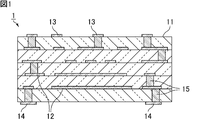
- FIG. 1 is a cross-sectional view schematically showing an example of a multilayer ceramic substrate.
- FIG. 2 is a cross-sectional view schematically showing an example of a multilayer ceramic capacitor.
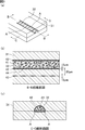
- 3 (a) is a perspective view schematically showing the vicinity of the inner conductor layer of the ceramic electronic component of the present invention
- FIG. 3 (b) is a cross-sectional view taken along the line BB of FIG. 3 (a)
- FIG. 3C is a cross-sectional view taken along the line CC of FIG. 4A to 4D are reflected electron images and Ti element mapping images in the vicinity of the inner conductor layers of the ceramic electronic components S-1 to S-4.
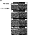
- FIGS. 5A to 5D are reflected electron images and Ti element mapping images of the entire ceramic electronic components S-1 to S-4.
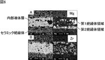
- FIG. 6A is a reflected electron image and Mg element mapping layer near the inner conductor layer of the ceramic electronic component S-11
- FIG. 6B is a reflected electron image and Zr element near the inner conductor layer of the ceramic electronic component S-12. This is a mapping image.
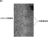
- FIG. 7 is a photomicrograph of the exposed surface of the ceramic electronic component S-4.
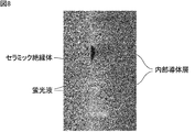
- FIG. 8 is a photomicrograph of the exposed surface of the ceramic electronic component S-15.
- the ceramic electronic component of the present invention and the method for manufacturing the ceramic electronic component will be described.
- the present invention is not limited to the following configurations, and can be applied with appropriate modifications without departing from the scope of the present invention.
- a combination of two or more of the individual desirable configurations of the present invention described below is also the present invention.
- Each embodiment shown below is an illustration, and it cannot be overemphasized that a partial substitution or combination of composition shown in a different embodiment is possible.
- FIG. 1 is a cross-sectional view schematically showing an example of a multilayer ceramic substrate.
- a multilayer ceramic substrate 1 shown in FIG. 1 includes a ceramic insulator 11 in which a plurality of ceramic layers are laminated, and an internal conductor layer 12 provided inside the ceramic insulator 11.
- the internal conductor layer 12 is disposed between the ceramic layers as a wiring conductor, and is formed substantially parallel to the main surface of the ceramic insulator 11.
- the multilayer ceramic substrate 1 is provided as an external conductor layer 13 provided on one main surface of the multilayer ceramic substrate 1 and on the other main surface of the multilayer ceramic substrate 1 as wiring conductors other than the internal conductor layer 12.
- a chip component (not shown) is mounted on one main surface of the multilayer ceramic substrate 1 in a state of being electrically connected to the external conductor layer 13.
- the chip component mounted on the multilayer ceramic substrate 1 may be the ceramic electronic component of the present invention.
- the external conductor layer 14 formed on the other main surface of the multilayer ceramic substrate 1 is used as an electrical connection means when the multilayer ceramic substrate 1 on which chip components are mounted is mounted on a mother board (not shown).
- the ceramic electronic component of the present invention is not limited to a multilayer ceramic substrate, and can be applied to a chip component mounted on the multilayer ceramic substrate, for example, a multilayer ceramic electronic component such as a multilayer ceramic capacitor, a multilayer inductor, and a multilayer filter.
- a multilayer ceramic electronic component such as a multilayer ceramic capacitor, a multilayer inductor, and a multilayer filter.
- the present invention can be applied to various ceramic electronic components other than the multilayer ceramic electronic component.
- FIG. 2 is a cross-sectional view schematically showing an example of a multilayer ceramic capacitor.
- the multilayer ceramic capacitor 2 shown in FIG. 2 includes a ceramic insulator 21 in which a plurality of dielectric layers are stacked, and inner layer electrodes 22a to 22f as internal conductor layers provided inside the ceramic insulator 21. Yes.
- the inner layer electrodes 22a to 22f are disposed between the dielectric layers, and are formed substantially parallel to the main surface of the ceramic insulator 21.
- An external electrode 23 a as an external conductor is formed on one end face of the ceramic insulator 21, and an external electrode 23 b as an external conductor is formed on the other end face of the ceramic insulator 21.
- the inner layer electrodes 22a to 22f are juxtaposed in the stacking direction.
- the inner layer electrodes 22a, 22c and 22e are exposed at one end face of the ceramic insulator 21, and are electrically connected to the outer electrode 23a.
- the inner layer electrodes 22b, 22d and 22f are exposed at the other end face of the ceramic insulator 21 and are electrically connected to the outer electrode 23b.
- produces between the opposing surfaces of inner layer electrode 22a, 22c, and 22e and inner layer electrode 22b, 22d, and 22f.
- the ceramic electronic component of the present invention preferably has a structure in which the inner conductor layer is exposed on the surface of the ceramic insulator or a structure in which the inner conductor layer is covered with an outer conductor.
- the external conductor is provided on the surface of the ceramic insulator, and may be a metal case or the like provided for electromagnetic shielding in addition to the external electrode described above.
- the ceramic insulator constituting the ceramic electronic component of the present invention preferably contains a low-temperature sintered ceramic material.
- the low-temperature sintered ceramic material means a material that can be sintered at a firing temperature of 1000 ° C. or less and can be co-fired with Ag or Cu among ceramic materials.
- Examples of the low-temperature sintered ceramic material included in the ceramic insulator include a glass composite low-temperature sintered ceramic material obtained by mixing borosilicate glass with a ceramic material such as quartz, alumina, and forsterite, ZnO—MgO—Al 2 Crystallized glass-based low-temperature sintered ceramic materials using O 3 —SiO 2 -based crystallized glass, BaO—Al 2 O 3 —SiO 2 based ceramic materials and Al 2 O 3 —CaO—SiO 2 —MgO—B 2
- Non-glass type low-temperature sintered ceramic material using O 3 type ceramic material or the like can be used.
- the internal conductor layer constituting the ceramic electronic component of the present invention contains a metal and a metal oxide.
- the metal contained in the inner conductor layer include Au, Ag, Cu, Pt, Ta, W, Ni, Fe, Cr, Mo, Ti, Pd, Ru, and an alloy mainly composed of one of these metals. Etc.
- the internal conductor layer preferably contains Au, Ag, or Cu as the metal, and more preferably contains Ag or Cu. Since Au, Ag, and Cu have low resistance, they are particularly suitable when the ceramic electronic component is used for high frequency.
- the metal oxide contained in the inner conductor layer contains at least one metal element selected from the group consisting of Ti, Mg, and Zr, and representative materials include TiO 2 , MgO, and ZrO 2. It is done. These metal oxides may be one kind or two or more kinds.
- the internal conductor layer preferably contains a metal oxide containing a Ti element such as TiO 2 as a metal oxide.
- the first insulator region discontinuous with the ceramic insulator is dispersed inside the inner conductor layer, and the second insulator region is present around the inner conductor layer.
- the first insulator region includes at least one metal element selected from the group consisting of Ti, Mg, and Zr, and the second insulator region is the same as the metal element included in the first insulator region. Contains metal elements.
- the metal element contained in the first insulator region and the second insulator region coincides with the metal element constituting the metal oxide contained in the internal conductor layer. That is, when the metal oxide contained in the internal conductor layer is a metal oxide containing Ti, such as TiO 2 , the metal element contained in the first insulator region and the second insulator region is Ti, When the metal oxide contained in the conductor layer is a metal oxide containing Mg, such as MgO, the metal element contained in the first insulator region and the second insulator region is Mg, and is contained in the inner conductor layer.
- a metal oxide containing Ti such as TiO 2
- Mg metal oxide containing Mg
- the metal oxide to be obtained is a metal oxide containing Zr, for example, ZrO 2
- the metal element contained in the first insulator region and the second insulator region is Zr.
- FIG. 3 (a) is a perspective view schematically showing the vicinity of the inner conductor layer of the ceramic electronic component of the present invention
- FIG. 3 (b) is a cross-sectional view taken along the line BB of FIG. 3 (a)
- FIG. 3C is a cross-sectional view taken along the line CC of FIG. 3A and 3B show an example in which one end of the internal conductor layer 32 is exposed on the surface of the ceramic insulator 31.
- FIG. 3B and FIG. 3C the ceramic insulator 31 and the discontinuous first insulator regions 41 are dispersed inside the inner conductor layer 32, and the inner conductor layer 32.
- the second insulator region 42 is present around the area.
- each region can be a first insulator region and a second insulator region.
- the first insulator region is a discontinuous region with the ceramic insulator. That is, the first insulator region is a region that is not connected to the ceramic insulator outside the inner conductor layer and is independent of the ceramic insulator surrounded by the metal of the inner conductor layer.
- the first insulator region is composed of a plurality of small regions, and each small region exists in a dispersed manner. The size of each small region is not particularly limited, and the size of each small region may be the same or different.
- the second insulator region is preferably uniformly present around the inner conductor layer, but may not be present at a part of the periphery of the inner conductor layer.
- region should just exist between an internal conductor layer and a ceramic insulator.
- region exists in an area
- FIG. 3B shows an example in which the second insulator region 42 exists in a region having a thickness of 3 ⁇ m between the inner conductor layer 32 and the ceramic insulator 31.
- the ceramic insulator preferably contains the same metal element as that contained in the first insulator region and the second insulator region. That is, when the metal element contained in the first insulator region and the second insulator region is Ti, the ceramic insulator preferably contains a Ti element, and the first insulator region and the second insulator region include When the metal element contained is Mg, the ceramic insulator preferably contains Mg element, and when the metal element contained in the first insulator region and the second insulator region is Zr, the ceramic insulator It is preferable that the body contains a Zr element. When two or more kinds of metal elements are included in the first insulator region and the second insulator region, the ceramic insulator only needs to include at least one of the metal elements.
- the concentration of the metal element contained in the ceramic insulator is lower than the concentration of the metal element in the first insulator region and lower than the concentration of the metal element in the second insulator region. It is preferable.
- the concentration of the metal element contained in the ceramic insulator is a 3 ⁇ m thick region (region 43 in FIG. 3B) that is 20 ⁇ m away from the interface between the inner conductor layer and the second insulator region. It is set as the density
- the concentration of the metal element contained in the ceramic insulator is lower than the concentration of the metal element in the first insulator region and lower than the concentration of the metal element in the second insulator region.
- the interface between the inner conductor layer and the second insulator region is the strength of the element (for example, Cu) of the metal component contained in the inner conductor layer when elemental analysis by WDX is performed under the conditions described in the examples.
- the length of the gap generated in the portion (the portion A in FIGS. 3A and 3C) of the lower surface of the inner conductor layer that is in contact with the upper surface of the inner conductor layer is 100 ⁇ m.
- the following is preferable.
- the length of the gap is 0 ⁇ m, that is, no gap is generated in the portion.
- the surface on which the inner conductor layer is formed is referred to as “the lower surface of the inner conductor layer”, and the other surface is referred to as “the upper surface of the inner conductor layer”.
- the bottom surface of the inner conductor layer in contact with the ceramic layer corresponds to the “lower surface of the inner conductor layer”, and the plane facing the bottom surface and The side surfaces collectively correspond to the “upper surface of the inner conductor layer”.
- the length of the gap is measured by measuring the length of the fluorescent liquid that has entered between the internal conductor layer and the ceramic insulator after impregnating the ceramic electronic component with the fluorescent liquid, as will be described in Examples. Is required.
- the ceramic electronic component of the present invention is preferably manufactured as follows.
- a plurality of green sheets including a raw material powder for a ceramic insulator is prepared.
- the green sheet is obtained by forming a slurry containing a ceramic raw material powder such as a low-temperature sintered ceramic material, an organic binder, and a solvent into a sheet shape by a doctor blade method or the like.
- the slurry may contain various additives such as a dispersant and a plasticizer.
- the raw material powder for the ceramic insulator preferably contains SiO 2 , Al 2 O 3 and a Ba compound. Furthermore, the raw material powder for the ceramic insulator more preferably contains the same metal element as the metal element contained in the conductor paste described later.
- a powder containing SiO 2 , Al 2 O 3 , and BaCO 3 is preferably used, and SiO 2 , Al 2 O 3 , BaCO 3 , More preferably, a powder containing at least one selected from the group consisting of TiO 2 , Mg (OH) 2 and ZrO 2 is used. By heating, BaCO 3 changes to BaO and Mg (OH) 2 changes to MgO. Instead of Mg (OH) 2 powder, MgO powder may be used.
- a conductor paste containing a metal powder, a metal oxide powder or a metal oxide precursor powder, and an organic vehicle is prepared.
- the metal powder Cu powder is preferably used.
- the organic vehicle for example, ethyl cellulose resin, acrylic resin, polyvinyl butyral resin, and the like can be used, and it is preferable to use ethyl cellulose resin.
- the metal oxide powder or metal oxide precursor powder contains at least one metal element selected from the group consisting of Ti, Mg, and Zr.
- the metal oxide precursor is changed to a metal oxide by heating.
- a powder containing at least one selected from the group consisting of TiO 2 , Mg (OH) 2 and ZrO 2 can be used as the metal oxide powder.
- TiO 2 powder By heating, Mg (OH) 2 changes to MgO.
- MgO powder may be used.
- the specific surface area (SSA) of the metal oxide powder or metal oxide precursor powder is preferably 6 m 2 / g or more, more preferably 20 m 2 / g or more, and still more preferably 50 m 2 / g or more.
- the specific surface area of the metal oxide powder or metal oxide precursor powder is preferably 90 m 2 / g or less.
- the specific surface area of the TiO 2 powder is preferably in the above range.
- the specific surface area equivalent particle diameter of the metal oxide powder or metal oxide precursor powder is D Osf [nm] and the volume-based median diameter of the metal powder is D M50 [nm]
- D M50 / D Osf ⁇ 105.5 is preferable, and 18.8 ⁇ D M50 / D Osf ⁇ 105.5 is more preferable.
- D M50 / D Osf is preferably in the above range.
- the specific surface area equivalent particle diameter D Osf [nm] of the metal oxide powder or metal oxide precursor powder is the specific surface area of the metal oxide powder or metal oxide precursor powder measured by the BET 1-point method.
- the volume-based median diameter D M50 [nm] of the metal powder is a value measured using a laser diffraction / scattering particle size distribution measuring device (LA series manufactured by Horiba, Ltd.).
- the content of the metal oxide powder or metal oxide precursor powder in the conductor paste is preferably 1.5% by weight or more, more preferably 2.0% by weight or more, further preferably 2.5% by weight or more, 4.0 weight% or less is preferable and 3.5 weight% or less is more preferable.
- the sintering start temperature of the metal powder is preferably equal to or lower than the sintering start temperature of the green sheet.
- the sintering start temperature of the metal powder and the green sheet is a temperature at which the main shrinkage temperature range, that is, the shrinkage amount is maximum in a temperature range of 400 ° C. or more and 1000 ° C. or less using a thermomechanical measurement apparatus (TMA). This is the temperature indicated by the intersection of the two lines when the tangent line of the TMA curve in the region and the tangent line of the TMA curve in the range of 600 ° C. to 700 ° C. are drawn.
- TMA thermomechanical measurement apparatus
- a conductor paste film serving as an internal conductor layer is formed. If necessary, a conductor paste film to be an external conductor layer and a conductor paste body to be a via conductor are formed on a specific green sheet. As a conductor paste for forming the outer conductor layer and the via conductor, it is preferable to use a conductor paste for forming the inner conductor layer.
- the raw laminate is preferably produced by laminating green sheets previously formed into a sheet shape, but is produced by repeatedly forming the ceramic slurry into a sheet shape at the same place. May be.
- the metal powder is sintered before the metal oxide component derived from the metal oxide powder or the metal oxide precursor powder diffuses into the ceramic insulator.
- the first insulator region and the second insulator region described above can be formed by retaining the oxide inside the inner conductor layer and between the inner conductor layer and the ceramic insulator. Thereby, shrinkage
- a constrained green sheet mainly composed of an inorganic material (Al 2 O 3 or the like) that does not substantially sinter at the sintering temperature of the raw laminate is prepared, and the raw laminate is prepared.
- the raw laminate may be fired with a constrained green sheet placed on the outermost surface of the body.
- the constrained green sheet does not sinter substantially at the time of firing, so that the shrinkage does not occur, and acts to suppress the shrinkage in the main surface direction with respect to the laminate.
- the dimensional accuracy of the ceramic electronic component can be increased.
- a plated layer may be formed on the surface of the fired external conductor by performing electrolytic plating or electroless plating.
- An organic binder, a dispersant, and a plasticizer were added to the raw material powder, and mixed and ground so that the average particle size (D 50 ) of the raw material powder was 1.5 ⁇ m or less to obtain a ceramic slurry.
- the ceramic slurry was formed into a sheet shape on a base film by a doctor blade method and dried to obtain a green sheet having a thickness adjusted to 20 ⁇ m after firing.
- the particle size (D M10 , D M50 and D M90 ) of the metal powder in Table 1 was measured using a laser diffraction / scattering type particle size distribution measuring apparatus (LA series manufactured by Horiba, Ltd.). As a measurement solvent, a mixture of ethyl alcohol and isopropyl alcohol was used.
- the SSA (specific surface area) of the metal powder and metal oxide powder in Tables 1 and 2 was measured using an SSA measuring apparatus (trade name: Macsorb (registered trademark) manufactured by Mountech) with a BET 1-point method using N 2 gas.
- the density of the metal powder and metal oxide powder in Tables 1 and 2 was measured using a dry automatic densimeter (trade name Accupic Series, manufactured by Shimadzu Corporation).
- the density of the organic vehicle in Table 3 was measured using a specific gravity cup (manufactured by Yasuda Seiki).
- the starting materials shown in Tables 1 to 3 were prepared so as to have the composition ratios shown in Table 4, and dispersed with a three-roll mill to obtain conductor pastes P-1 to P-15.
- FIGS. 5A to 5D are reflected electron images and Ti element mapping images of the entire ceramic electronic components S-1 to S-4. 5A to 5D, the left side is a reflected electron image, and the right side is a Ti element mapping image.
- 5A to 5D as in FIGS. 4A to 4D, the ceramic insulator and the discontinuous first insulator region exist in the inner conductor layer and are distributed around the inner conductor layer. It can be confirmed that the second insulator region exists. On the other hand, in the region 20 ⁇ m away from the interface between the inner conductor layer and the second insulator region, it can be confirmed that the strength of the Ti element is lower than that in the first insulator region and the second insulator region. Therefore, it can be seen that the concentration of Ti element contained in the ceramic insulator is lower than the concentration of Ti element in the first insulator region and the second insulator region.
- the ceramic electronic components S-13 and S-14 in which the inner conductor layer is formed using the conductor pastes P-13 and P-14 in which the content of the TiO 2 powder, which is a powder, is changed are the same as the ceramic electronic components S-3 and S-14.
- the ceramic insulator and the discontinuous first insulator region exist in the inner conductor layer, and the second insulator region exists around the inner conductor layer.
- FIG. 6A is a reflected electron image and Mg element mapping layer near the inner conductor layer of the ceramic electronic component S-11
- FIG. 6B is a reflected electron image and Zr element near the inner conductor layer of the ceramic electronic component S-12.
- This is a mapping image.
- 6A and 6B the left side is a reflected electron image, and the right side is a mapping image of Mg element or Zr element.
- the second insulator region does not exist in a part of the periphery of the inner conductor layer
- the first insulator region discontinuous with the ceramic insulator is dispersed inside the inner conductor layer, and the second insulator region is present around the inner conductor layer. It can be confirmed.
- the presence of the first insulator region and the second insulator region could not be confirmed. This is presumably because the metal oxide powder contained in the conductor paste reacted with the raw material powder of the ceramic insulator.
- the presence of the first insulator region and the second insulator region can also be confirmed in the ceramic electronic component S-15 in which the inner conductor layer is formed using the conductor paste P-15 that does not contain the metal oxide powder. could not.
- each ceramic electronic component was vacuum impregnated with a fluorescent solution and then dried using a dryer. Thereafter, the ceramic electronic component was polished using a mechanical polishing machine until the surface including the inner conductor layer was exposed. The polished surface was confirmed using a microscope with an Hg light source, and it was confirmed whether the fluorescent solution had entered between the internal conductor layer and the ceramic insulator.
- FIG. 7 is a photomicrograph of the exposed surface of the ceramic electronic component S-4
- FIG. 8 is a photomicrograph of the exposed surface of the ceramic electronic component S-15.
- the fluorescent solution is not infiltrated as shown in FIG. 7, whereas the first insulator region and the second insulator region In the ceramic electronic component S-15 without the presence of the fluorescent liquid, it can be confirmed that the fluorescent liquid has entered as shown in FIG. From the above results, it can be seen that the formation of the gap between the internal conductor layer and the ceramic insulator is suppressed by forming the first insulator region and the second insulator region.
- Multilayer ceramic substrate (ceramic electronic parts) 2 Multilayer ceramic capacitors (ceramic electronic components) 11, 21, 31 Ceramic insulators 12, 32 Inner conductor layers 13, 14 Outer conductor layer 15 Via conductors 22a, 22b, 22c, 22d, 22e, 22f Inner layer electrode (inner conductor layer) 23a, 23b External electrode 41 First insulator region 42 Second insulator region 43 3 ⁇ m thick region 44 away from the interface between the inner conductor layer and the second insulator region 44 The inner conductor layer and the second insulator region Interface A of the lower surface of the inner conductor layer that is in contact with the upper surface of the inner conductor layer
Landscapes
- Engineering & Computer Science (AREA)
- Power Engineering (AREA)
- Manufacturing & Machinery (AREA)
- Microelectronics & Electronic Packaging (AREA)
- Chemical & Material Sciences (AREA)
- Materials Engineering (AREA)
- Ceramic Capacitors (AREA)
- Fixed Capacitors And Capacitor Manufacturing Machines (AREA)
- Ceramic Engineering (AREA)
- Inorganic Chemistry (AREA)
Abstract
本発明のセラミック電子部品は、セラミック絶縁体と、上記セラミック絶縁体の内部に設けられた内部導体層とを備えるセラミック電子部品であって、上記内部導体層は、金属と、Ti、Mg及びZrからなる群より選択される少なくとも1種の金属元素を含む金属酸化物とを含み、上記内部導体層の内部に、Ti、Mg及びZrからなる群より選択される少なくとも1種の金属元素を含み、上記セラミック絶縁体と不連続な第1絶縁体領域が分散して存在するとともに、上記内部導体層の周囲に、上記第1絶縁体領域に含まれる上記金属元素と同じ金属元素を含む第2絶縁体領域が存在することを特徴とする。
Description
本発明は、セラミック電子部品及びセラミック電子部品の製造方法に関する。
多層セラミック基板及び積層セラミックコンデンサ等のセラミック電子部品は、セラミック絶縁体と、セラミック絶縁体に埋設された内部導体と、セラミック絶縁体の外表面に設けられた外部導体とを備えている。このようなセラミック電子部品は、通常、セラミック絶縁体の原料粉末を含むグリーンシート上に、導体ペーストを用いて内部導体又は外部導体となる導体ペースト膜を形成し、次いで、導体ペースト膜が形成されたグリーンシートを複数枚積層して生の積層体を形成し、この生の積層体を焼成することにより得られる。さらに、耐熱性及びはんだ濡れ性等の向上を目的として、めっき処理を行うことによって、外部導体の表面にめっき層が形成される。
上記の方法によってセラミック電子部品を製造する際、焼成時に導体ペースト及びグリーンシートはどちらも収縮し、両者の収縮挙動の違いによって、内部導体とセラミック絶縁体との間に空隙が形成される場合がある。この場合、めっき液等の液体が上記空隙に浸入し、その結果、セラミック電子部品の電気特性が低下する等、信頼性低下を招くおそれがある。
そこで、めっき液等の液体の浸入を防止する手段として、特許文献1及び特許文献2に記載の方法が提案されている。特許文献1には、焼結磁性体、誘電体等のセラミック表面部分の細孔へ合成樹脂を真空中で含浸させることにより細孔を塞ぐ方法、特許文献2には、湿式めっきを行う工程中はセラミック素体及び端子電極の空隙に有機溶剤を充填し、該工程が終了した後に有機溶剤を揮発除去する方法がそれぞれ記載されている。
特許文献1及び特許文献2に記載の方法は、後処理によって空隙を埋める方法であるため、セラミック電子部品を製造するための工数が増加してしまう。さらに、特許文献1で用いる樹脂材料はセラミック材料と熱膨張係数が異なるため、セラミック電子部品に熱衝撃が加わった際、両者の間での剥離又はクラックの発生を招くおそれがある。また、特許文献2のように有機溶剤を用いる方法は、めっき処理時に一時的に空隙を塞ぐ方法であるため、有機溶剤が揮発した後には液体が浸入し得る空隙が残存することになる。
本発明は上記の問題を解決するためになされたものであり、内部導体層とセラミック絶縁体との間で空隙が形成されにくく、外部からの液体の浸入を防止することができるセラミック電子部品、及び、該セラミック電子部品の製造方法を提供することを目的とする。
上記目的を達成するため、本発明のセラミック電子部品は、セラミック絶縁体と、上記セラミック絶縁体の内部に設けられた内部導体層とを備えるセラミック電子部品であって、上記内部導体層は、金属と、Ti、Mg及びZrからなる群より選択される少なくとも1種の金属元素を含む金属酸化物とを含み、上記内部導体層の内部に、Ti、Mg及びZrからなる群より選択される少なくとも1種の金属元素を含み、上記セラミック絶縁体と不連続な第1絶縁体領域が分散して存在するとともに、上記内部導体層の周囲に、上記第1絶縁体領域に含まれる上記金属元素と同じ金属元素を含む第2絶縁体領域が存在することを特徴とする。
本発明のセラミック電子部品では、内部導体層の内部及び周囲に、Ti、Mg及びZrからなる群より選択される少なくとも1種の金属元素を含む第1絶縁体領域及び第2絶縁体領域がそれぞれ存在している。これは、セラミック電子部品を製造するために焼成する際、内部導体層に含まれる金属酸化物の成分が、セラミック絶縁体へ拡散せず、内部導体層の内部、及び、内部導体層とセラミック絶縁体との間に留まることを意味している。これにより、焼成時における内部導体層の収縮が抑制され、内部導体層とセラミック絶縁体との間に空隙が形成されにくくなる。
このように、本発明のセラミック電子部品では、内部導体層とセラミック絶縁体との間での空隙の形成を抑制することができるため、めっき液等の液体の外部からの浸入を防止することができる。その結果、マイグレーション等の発生が抑制され、導体間のショートが低減するため、信頼性の向上に繋がる。さらに、液体の浸入が原因となってセラミック電子部品の実装時に問題となる、外部導体の膨張、半田爆ぜ、半田内部での空隙の形成、外部導体の変色等の不良を低減することもできる。
このように、本発明のセラミック電子部品では、内部導体層とセラミック絶縁体との間での空隙の形成を抑制することができるため、めっき液等の液体の外部からの浸入を防止することができる。その結果、マイグレーション等の発生が抑制され、導体間のショートが低減するため、信頼性の向上に繋がる。さらに、液体の浸入が原因となってセラミック電子部品の実装時に問題となる、外部導体の膨張、半田爆ぜ、半田内部での空隙の形成、外部導体の変色等の不良を低減することもできる。
本発明のセラミック電子部品において、上記セラミック絶縁体は、上記第1絶縁体領域及び上記第2絶縁体領域に含まれる上記金属元素と同じ金属元素を含むことが好ましい。
セラミック絶縁体が第1絶縁体領域及び第2絶縁体領域に含まれる金属元素と同じ金属元素を含んでいると、内部導体層の焼結挙動がセラミック絶縁体の焼結挙動に近くなるため、内部導体層とセラミック絶縁体との間での空隙の形成をさらに抑制することができる。
セラミック絶縁体が第1絶縁体領域及び第2絶縁体領域に含まれる金属元素と同じ金属元素を含んでいると、内部導体層の焼結挙動がセラミック絶縁体の焼結挙動に近くなるため、内部導体層とセラミック絶縁体との間での空隙の形成をさらに抑制することができる。
セラミック絶縁体が第1絶縁体領域及び第2絶縁体領域に含まれる金属元素と同じ金属元素を含む場合、上記セラミック絶縁体に含まれる上記金属元素の濃度は、上記第1絶縁体領域における上記金属元素の濃度よりも低く、上記第2絶縁体領域における上記金属元素の濃度よりも低いことが好ましい。
これは、セラミック絶縁体が第1絶縁体領域及び第2絶縁体領域に含まれる金属元素と同じ金属元素を含む場合であっても、内部導体層に含まれる金属酸化物の成分が内部導体層の内部、及び、内部導体層とセラミック絶縁体との間に留まることを意味する。したがって、焼成時における内部導体層の収縮が抑制され、内部導体層とセラミック絶縁体との間に空隙が形成されにくくなる。
これは、セラミック絶縁体が第1絶縁体領域及び第2絶縁体領域に含まれる金属元素と同じ金属元素を含む場合であっても、内部導体層に含まれる金属酸化物の成分が内部導体層の内部、及び、内部導体層とセラミック絶縁体との間に留まることを意味する。したがって、焼成時における内部導体層の収縮が抑制され、内部導体層とセラミック絶縁体との間に空隙が形成されにくくなる。
本発明のセラミック電子部品において、上記内部導体層は、上記セラミック絶縁体の表面に露出していることが好ましい。また、本発明のセラミック電子部品は、上記セラミック絶縁体の表面に設けられた外部導体をさらに備え、上記内部導体層は、上記外部導体によって被覆されていることも好ましい。
このように、セラミック電子部品が外部から液体が浸入しやすい構造であっても、内部導体層とセラミック絶縁体との間での空隙の形成を抑制することができるため、めっき液等の液体の外部からの浸入を防止することができる。
このように、セラミック電子部品が外部から液体が浸入しやすい構造であっても、内部導体層とセラミック絶縁体との間での空隙の形成を抑制することができるため、めっき液等の液体の外部からの浸入を防止することができる。
本発明のセラミック電子部品においては、上記内部導体層の下面のうち、上記内部導体層の上面と接する部分に生じる空隙の長さが100μm以下であることが好ましい。
本発明のセラミック電子部品においては、内部導体層とセラミック絶縁体との間の中でも空隙が形成されやすい、内部導体層の下面のうち、内部導体層の上面と接する部分に生じる空隙の形成を抑制することができる。
本発明のセラミック電子部品においては、内部導体層とセラミック絶縁体との間の中でも空隙が形成されやすい、内部導体層の下面のうち、内部導体層の上面と接する部分に生じる空隙の形成を抑制することができる。
本発明のセラミック電子部品の製造方法は、上記セラミック電子部品の製造方法であって、セラミック絶縁体の原料粉末を含む複数のグリーンシートを準備する工程と、金属粉末と、金属酸化物粉末又は金属酸化物前駆体粉末と、有機ビヒクルとを含み、上記金属酸化物粉末又は上記金属酸化物前駆体粉末がTi、Mg及びZrからなる群より選択される少なくとも1種の金属元素を含む導体ペーストを準備する工程と、上記グリーンシートの少なくとも1枚の主面に上記導体ペーストを塗布することによって、内部導体層となる導体ペースト膜を形成する工程と、複数の上記グリーンシートが積層されるとともに、上記導体ペースト膜が上記グリーンシート間に形成された生の積層体を作製する工程と、上記生の積層体を焼成する工程と、を備えることを特徴とする。
本発明のセラミック電子部品の製造方法では、金属酸化物粉末又は金属酸化物前駆体粉末に由来する金属酸化物の成分がセラミック絶縁体へ拡散する前に金属粉末を焼結させることで、上記金属酸化物を内部導体層の内部、及び、内部導体層とセラミック絶縁体との間に留め、上述した第1絶縁体領域及び第2絶縁体領域を形成することができる。これにより、焼成時における内部導体層の収縮を抑制することができる。その結果、内部導体層とセラミック絶縁体との間に空隙が形成されにくく、外部からの液体の浸入を防止することができるセラミック電子部品を製造することができる。
本発明のセラミック電子部品の製造方法においては、上記金属酸化物粉末又は上記金属酸化物前駆体粉末の比表面積が、6m2/g以上90m2/g以下であることが好ましい。
導体ペーストに含まれる金属酸化物粉末又は金属酸化物前駆体粉末の比表面積が上記範囲であると、焼結した金属粉末同士の間に金属酸化物粉末又は金属酸化物前駆体粉末が閉じ込められやすくなる。つまり、内部導体層に含まれる金属酸化物の成分がセラミック絶縁体へ拡散しにくくなるため、焼成時における内部導体層の収縮がさらに抑制される。
導体ペーストに含まれる金属酸化物粉末又は金属酸化物前駆体粉末の比表面積が上記範囲であると、焼結した金属粉末同士の間に金属酸化物粉末又は金属酸化物前駆体粉末が閉じ込められやすくなる。つまり、内部導体層に含まれる金属酸化物の成分がセラミック絶縁体へ拡散しにくくなるため、焼成時における内部導体層の収縮がさらに抑制される。
本発明のセラミック電子部品の製造方法においては、上記金属酸化物粉末又は上記金属酸化物前駆体粉末の比表面積換算粒径をDOsf[nm]、上記金属粉末の体積基準メディアン径をDM50[nm]としたとき、2.28≦DM50/DOsf≦105.5であることが好ましい。
金属粉末の粒径に対する金属酸化物粉末又は金属酸化物前駆体粉末の粒径が小さいと、焼結した金属粉末同士の間に金属酸化物粉末又は金属酸化物前駆体粉末が閉じ込められやすくなる。つまり、内部導体層に含まれる金属酸化物の成分がセラミック絶縁体へ拡散しにくくなるため、焼成時における内部導体層の収縮がさらに抑制される。
金属粉末の粒径に対する金属酸化物粉末又は金属酸化物前駆体粉末の粒径が小さいと、焼結した金属粉末同士の間に金属酸化物粉末又は金属酸化物前駆体粉末が閉じ込められやすくなる。つまり、内部導体層に含まれる金属酸化物の成分がセラミック絶縁体へ拡散しにくくなるため、焼成時における内部導体層の収縮がさらに抑制される。
本発明のセラミック電子部品の製造方法においては、上記金属粉末の焼結開始温度が、上記グリーンシートの焼結開始温度以下であることが好ましい。
グリーンシートの焼結が低温で開始すると、セラミック絶縁体の液相成分が導体ペースト中の金属酸化物と反応してしまい、第1絶縁体領域及び第2絶縁体領域が形成されないおそれがある。したがって、金属粉末の焼結開始温度をグリーンシートの焼結開始温度以下とすることにより、第1絶縁体領域及び第2絶縁体領域を確実に形成することができる。
グリーンシートの焼結が低温で開始すると、セラミック絶縁体の液相成分が導体ペースト中の金属酸化物と反応してしまい、第1絶縁体領域及び第2絶縁体領域が形成されないおそれがある。したがって、金属粉末の焼結開始温度をグリーンシートの焼結開始温度以下とすることにより、第1絶縁体領域及び第2絶縁体領域を確実に形成することができる。
本発明のセラミック電子部品の製造方法において、上記セラミック絶縁体の原料粉末は、SiO2とAl2O3とBa化合物とを含むことが好ましい。
上記の原料粉末は、1000℃以下の温度の焼成温度で焼結可能であり、AgやCuとの同時焼成が可能である。
上記の原料粉末は、1000℃以下の温度の焼成温度で焼結可能であり、AgやCuとの同時焼成が可能である。
本発明によれば、内部導体層とセラミック絶縁体との間で空隙が形成されにくく、外部からの液体の浸入を防止することができるセラミック電子部品、及び、該セラミック電子部品の製造方法を提供することができる。
以下、本発明のセラミック電子部品及びセラミック電子部品の製造方法について説明する。
しかしながら、本発明は、以下の構成に限定されるものではなく、本発明の要旨を変更しない範囲において適宜変更して適用することができる。
以下において記載する本発明の個々の望ましい構成を2つ以上組み合わせたものもまた本発明である。
以下に示す各実施形態は例示であり、異なる実施形態で示した構成の部分的な置換又は組み合わせが可能であることは言うまでもない。
しかしながら、本発明は、以下の構成に限定されるものではなく、本発明の要旨を変更しない範囲において適宜変更して適用することができる。
以下において記載する本発明の個々の望ましい構成を2つ以上組み合わせたものもまた本発明である。
以下に示す各実施形態は例示であり、異なる実施形態で示した構成の部分的な置換又は組み合わせが可能であることは言うまでもない。
本発明のセラミック電子部品の一実施形態として、多層セラミック基板を例にとって説明する。
図1は、多層セラミック基板の一例を模式的に示す断面図である。
図1に示す多層セラミック基板1は、複数のセラミック層が積層されてなるセラミック絶縁体11と、セラミック絶縁体11の内部に設けられた内部導体層12とを備えている。内部導体層12は、配線導体として、セラミック層の間に配置されており、セラミック絶縁体11の主面に実質的に平行に形成されている。
さらに、多層セラミック基板1は、内部導体層12以外の配線導体として、多層セラミック基板1の一方主面上に設けられた外部導体層13と、多層セラミック基板1の他方主面上に設けられた外部導体層14と、内部導体層12、外部導体層13及び外部導体層14のいずれかと電気的に接続され、かつセラミック層を厚み方向に貫通するように設けられたビア導体15とを備えている。
図1は、多層セラミック基板の一例を模式的に示す断面図である。
図1に示す多層セラミック基板1は、複数のセラミック層が積層されてなるセラミック絶縁体11と、セラミック絶縁体11の内部に設けられた内部導体層12とを備えている。内部導体層12は、配線導体として、セラミック層の間に配置されており、セラミック絶縁体11の主面に実質的に平行に形成されている。
さらに、多層セラミック基板1は、内部導体層12以外の配線導体として、多層セラミック基板1の一方主面上に設けられた外部導体層13と、多層セラミック基板1の他方主面上に設けられた外部導体層14と、内部導体層12、外部導体層13及び外部導体層14のいずれかと電気的に接続され、かつセラミック層を厚み方向に貫通するように設けられたビア導体15とを備えている。
多層セラミック基板1の一方主面上には、外部導体層13に電気的に接続された状態で、チップ部品(図示せず)が搭載される。多層セラミック基板1に搭載されるチップ部品が本発明のセラミック電子部品であってもよい。多層セラミック基板1の他方主面上に形成された外部導体層14は、チップ部品が搭載された多層セラミック基板1をマザーボード(図示せず)上に実装する際の電気的接続手段として用いられる。
本発明のセラミック電子部品は、多層セラミック基板に限らず、多層セラミック基板に搭載するチップ部品、例えば、積層セラミックコンデンサ、積層インダクタ、積層フィルタ等の積層セラミック電子部品に対して適用することが可能であり、また、積層セラミック電子部品以外の種々のセラミック電子部品に対して適用することも可能である。
図2は、積層セラミックコンデンサの一例を模式的に示す断面図である。
図2に示す積層セラミックコンデンサ2は、複数の誘電体層が積層されてなるセラミック絶縁体21と、セラミック絶縁体21の内部に設けられた内部導体層としての内層電極22a~22fとを備えている。内層電極22a~22fは、誘電体層の間に配置されており、セラミック絶縁体21の主面に実質的に平行に形成されている。セラミック絶縁体21の一方端面には外部導体としての外部電極23aが形成されており、セラミック絶縁体21の他方端面には外部導体としての外部電極23bが形成されている。
図2に示す積層セラミックコンデンサ2は、複数の誘電体層が積層されてなるセラミック絶縁体21と、セラミック絶縁体21の内部に設けられた内部導体層としての内層電極22a~22fとを備えている。内層電極22a~22fは、誘電体層の間に配置されており、セラミック絶縁体21の主面に実質的に平行に形成されている。セラミック絶縁体21の一方端面には外部導体としての外部電極23aが形成されており、セラミック絶縁体21の他方端面には外部導体としての外部電極23bが形成されている。
内層電極22a~22fは、積層方向に並設されている。内層電極22a、22c及び22eは、セラミック絶縁体21の一方端面に露出し、外部電極23aと電気的に接続されている。また、内層電極22b、22d及び22fは、セラミック絶縁体21の他方端面に露出し、外部電極23bと電気的に接続されている。そして、内層電極22a、22c及び22eと内層電極22b、22d及び22fとの対向面間で静電容量が発生する。
本発明のセラミック電子部品においては、内部導体層がセラミック絶縁体の表面に露出している構造、又は、内部導体層が外部導体によって被覆されている構造を有していることが好ましい。
なお、本発明のセラミック電子部品において、外部導体は、セラミック絶縁体の表面に設けられるものであり、上述の外部電極のほか、電磁シールド用に設けられる金属ケース等であってもよい。
なお、本発明のセラミック電子部品において、外部導体は、セラミック絶縁体の表面に設けられるものであり、上述の外部電極のほか、電磁シールド用に設けられる金属ケース等であってもよい。
本発明のセラミック電子部品を構成するセラミック絶縁体は、低温焼結セラミック材料を含むことが好ましい。
低温焼結セラミック材料とは、セラミック材料のうち、1000℃以下の焼成温度で焼結可能であり、AgやCuとの同時焼成が可能である材料を意味する。
低温焼結セラミック材料とは、セラミック材料のうち、1000℃以下の焼成温度で焼結可能であり、AgやCuとの同時焼成が可能である材料を意味する。
セラミック絶縁体に含まれる低温焼結セラミック材料としては、例えば、クオーツやアルミナ、フォルステライト等のセラミック材料にホウ珪酸ガラスを混合してなるガラス複合系低温焼結セラミック材料、ZnO-MgO-Al2O3-SiO2系の結晶化ガラスを用いた結晶化ガラス系低温焼結セラミック材料、BaO-Al2O3-SiO2系セラミック材料やAl2O3-CaO-SiO2-MgO-B2O3系セラミック材料等を用いた非ガラス系低温焼結セラミック材料等が挙げられる。
本発明のセラミック電子部品を構成する内部導体層は、金属と金属酸化物とを含む。
内部導体層に含まれる金属としては、例えば、Au、Ag、Cu、Pt、Ta、W、Ni、Fe、Cr、Mo、Ti、Pd、Ru及びこれらの金属の1種を主成分とする合金等が挙げられる。内部導体層は、金属として、Au、Ag又はCuを含むことが好ましく、Ag又はCuを含むことがより好ましい。Au、Ag及びCuは低抵抗であるため、特に、セラミック電子部品が高周波用途である場合に適している。
内部導体層に含まれる金属としては、例えば、Au、Ag、Cu、Pt、Ta、W、Ni、Fe、Cr、Mo、Ti、Pd、Ru及びこれらの金属の1種を主成分とする合金等が挙げられる。内部導体層は、金属として、Au、Ag又はCuを含むことが好ましく、Ag又はCuを含むことがより好ましい。Au、Ag及びCuは低抵抗であるため、特に、セラミック電子部品が高周波用途である場合に適している。
内部導体層に含まれる金属酸化物は、Ti、Mg及びZrからなる群より選択される少なくとも1種の金属元素を含むものであり、代表的な物質としてはTiO2、MgO及びZrO2が挙げられる。これらの金属酸化物は1種でもよく、2種以上であってもよい。内部導体層は、金属酸化物として、TiO2等のTi元素を含む金属酸化物を含むことが好ましい。
本発明のセラミック電子部品においては、内部導体層の内部に、セラミック絶縁体と不連続な第1絶縁体領域が分散して存在するとともに、内部導体層の周囲に、第2絶縁体領域が存在する。第1絶縁体領域は、Ti、Mg及びZrからなる群より選択される少なくとも1種の金属元素を含んでおり、第2絶縁体領域は、第1絶縁体領域に含まれる上記金属元素と同じ金属元素を含んでいる。
第1絶縁体領域及び第2絶縁体領域に含まれる金属元素は、内部導体層に含まれる金属酸化物を構成する金属元素と一致する。すなわち、内部導体層に含まれる金属酸化物がTiを含む金属酸化物、例えばTiO2である場合には、第1絶縁体領域及び第2絶縁体領域に含まれる金属元素がTiであり、内部導体層に含まれる金属酸化物がMgを含む金属酸化物、例えばMgOである場合には、第1絶縁体領域及び第2絶縁体領域に含まれる金属元素がMgであり、内部導体層に含まれる金属酸化物がZrを含む金属酸化物、例えばZrO2である場合には、第1絶縁体領域及び第2絶縁体領域に含まれる金属元素がZrである。内部導体層に2種以上の金属酸化物が含まれる場合、そのうちの少なくとも1種の金属酸化物が第1絶縁体領域及び第2絶縁体領域に含まれていればよい。
図3(a)は、本発明のセラミック電子部品の内部導体層付近を模式的に示す斜視図であり、図3(b)は、図3(a)のB-B線断面図であり、図3(c)は、図3(a)のC-C線断面図である。図3(a)及び図3(b)では、内部導体層32の一端がセラミック絶縁体31の表面に露出している例を示している。
図3(b)及び図3(c)に示すように、内部導体層32の内部に、セラミック絶縁体31と不連続な第1絶縁体領域41が分散して存在するとともに、内部導体層32の周囲に、第2絶縁体領域42が存在する。
図3(b)及び図3(c)に示すように、内部導体層32の内部に、セラミック絶縁体31と不連続な第1絶縁体領域41が分散して存在するとともに、内部導体層32の周囲に、第2絶縁体領域42が存在する。
本明細書においては、波長分散型X線分光分析(WDX)による元素分析によって、Ti、Mg及びZrからなる群より選択される少なくとも1種の金属元素が内部導体層の内部及び周囲に確認されれば、各領域を第1絶縁体領域及び第2絶縁体領域とすることができる。
本発明のセラミック電子部品において、第1絶縁体領域は、セラミック絶縁体と不連続な領域である。すなわち、第1絶縁体領域は、内部導体層の外側にあるセラミック絶縁体と繋がっておらず、内部導体層の金属に囲まれてセラミック絶縁体から独立した領域である。第1絶縁体領域は、複数の小領域から構成されており、それぞれの小領域は分散して存在している。それぞれの小領域のサイズは特に限定されず、また、それぞれの小領域のサイズは同じであってもよいし、異なっていてもよい。
本発明のセラミック電子部品において、第2絶縁体領域は、内部導体層の周囲に一様に存在することが好ましいが、内部導体層の周囲の一部に存在していなくてもよい。
また、第2絶縁体領域は、内部導体層とセラミック絶縁体との間に存在していればよい。中でも、第2絶縁体領域は、内部導体層とセラミック絶縁体との間、厚さ3μmの領域に存在することが好ましい。図3(b)では、第2絶縁体領域42が、内部導体層32とセラミック絶縁体31との間、厚さ3μmの領域に存在する例を示している。
また、第2絶縁体領域は、内部導体層とセラミック絶縁体との間に存在していればよい。中でも、第2絶縁体領域は、内部導体層とセラミック絶縁体との間、厚さ3μmの領域に存在することが好ましい。図3(b)では、第2絶縁体領域42が、内部導体層32とセラミック絶縁体31との間、厚さ3μmの領域に存在する例を示している。
本発明のセラミック電子部品において、セラミック絶縁体は、第1絶縁体領域及び第2絶縁体領域に含まれる金属元素と同じ金属元素を含むことが好ましい。すなわち、第1絶縁体領域及び第2絶縁体領域に含まれる金属元素がTiである場合には、セラミック絶縁体がTi元素を含むことが好ましく、第1絶縁体領域及び第2絶縁体領域に含まれる金属元素がMgである場合には、セラミック絶縁体がMg元素を含むことが好ましく、第1絶縁体領域及び第2絶縁体領域に含まれる金属元素がZrである場合には、セラミック絶縁体がZr元素を含むことが好ましい。第1絶縁体領域及び第2絶縁体領域に2種以上の金属元素が含まれる場合、そのうちの少なくとも1種の金属元素をセラミック絶縁体が含んでいればよい。
本発明のセラミック電子部品において、セラミック絶縁体に含まれる上記金属元素の濃度は、第1絶縁体領域における上記金属元素の濃度よりも低く、第2絶縁体領域における上記金属元素の濃度よりも低いことが好ましい。
本明細書において、セラミック絶縁体に含まれる上記金属元素の濃度は、内部導体層と第2絶縁体領域との界面から20μm離れた厚さ3μmの領域(図3(b)中の領域43)における上記金属元素の濃度とする。
上記領域において、上述のWDXによるTi、Mg及びZrからなる群より選択される少なくとも1種の金属元素の強度が第1絶縁体領域及び第2絶縁体領域における上記金属元素の強度よりも小さければ、セラミック絶縁体に含まれる上記金属元素の濃度は、第1絶縁体領域における上記金属元素の濃度よりも低く、第2絶縁体領域における上記金属元素の濃度よりも低いと言うことができる。
なお、内部導体層と第2絶縁体領域との界面とは、実施例で説明する条件でWDXによる元素分析を行った場合における、内部導体層に含まれる金属成分の元素(例えばCu)の強度が600未満となる部位を意味する。
上記領域において、上述のWDXによるTi、Mg及びZrからなる群より選択される少なくとも1種の金属元素の強度が第1絶縁体領域及び第2絶縁体領域における上記金属元素の強度よりも小さければ、セラミック絶縁体に含まれる上記金属元素の濃度は、第1絶縁体領域における上記金属元素の濃度よりも低く、第2絶縁体領域における上記金属元素の濃度よりも低いと言うことができる。
なお、内部導体層と第2絶縁体領域との界面とは、実施例で説明する条件でWDXによる元素分析を行った場合における、内部導体層に含まれる金属成分の元素(例えばCu)の強度が600未満となる部位を意味する。
本発明のセラミック電子部品においては、内部導体層の下面のうち、内部導体層の上面と接する部分(図3(a)及び図3(c)中のA部分)に生じる空隙の長さが100μm以下であることが好ましい。特に、上記空隙の長さは0μmであること、すなわち、上記部分に空隙が生じないことが好ましい。
本明細書においては、内部導体層が形成されている面を「内部導体層の下面」とし、それ以外の面を「内部導体層の上面」とする。例えば、形状が直方体である内部導体層がセラミック層上に形成されている場合、当該セラミック層と接する内部導体層の底面が「内部導体層の下面」に該当し、上記底面と対向する平面及び側面がまとめて「内部導体層の上面」に該当する。
なお、上記空隙の長さは、実施例で説明するように、セラミック電子部品に蛍光液を含浸させた後、内部導体層とセラミック絶縁体との間に侵入した蛍光液の長さを測定することによって求められる。
本明細書においては、内部導体層が形成されている面を「内部導体層の下面」とし、それ以外の面を「内部導体層の上面」とする。例えば、形状が直方体である内部導体層がセラミック層上に形成されている場合、当該セラミック層と接する内部導体層の底面が「内部導体層の下面」に該当し、上記底面と対向する平面及び側面がまとめて「内部導体層の上面」に該当する。
なお、上記空隙の長さは、実施例で説明するように、セラミック電子部品に蛍光液を含浸させた後、内部導体層とセラミック絶縁体との間に侵入した蛍光液の長さを測定することによって求められる。
本発明のセラミック電子部品は、好ましくは、以下のように製造される。
まず、セラミック絶縁体の原料粉末を含む複数のグリーンシートを準備する。
グリーンシートは、例えば低温焼結セラミック材料のようなセラミック原料の粉末と、有機バインダと溶剤とを含むスラリーを、ドクターブレード法等によってシート状に成形したものである。上記スラリーには、分散剤、可塑剤等の種々の添加剤が含まれていてもよい。
グリーンシートは、例えば低温焼結セラミック材料のようなセラミック原料の粉末と、有機バインダと溶剤とを含むスラリーを、ドクターブレード法等によってシート状に成形したものである。上記スラリーには、分散剤、可塑剤等の種々の添加剤が含まれていてもよい。
セラミック絶縁体の原料粉末は、SiO2とAl2O3とBa化合物とを含むことが好ましい。さらに、セラミック絶縁体の原料粉末は、後述する導体ペーストに含まれる金属元素と同じ金属元素を含むことがより好ましい。上記スラリーに含まれるセラミック原料の粉末としては、例えば、SiO2と、Al2O3と、BaCO3とを含む粉末を用いることが好ましく、SiO2と、Al2O3と、BaCO3と、TiO2、Mg(OH)2及びZrO2からなる群より選択される少なくとも1種とを含む粉末を用いることがより好ましい。加熱により、BaCO3はBaOに、Mg(OH)2はMgOに変化する。Mg(OH)2粉末に代えて、MgO粉末を用いてもよい。
別途、金属粉末と、金属酸化物粉末又は金属酸化物前駆体粉末と、有機ビヒクルとを含む導体ペーストを準備する。
金属粉末としては、Cu粉末を用いることが好ましい。また、有機ビヒクルとしては、例えば、エチルセルロース系樹脂、アクリル樹脂及びポリビニルブチラール樹脂等を用いることができ、中でもエチルセルロース系樹脂を用いることが好ましい。
金属粉末としては、Cu粉末を用いることが好ましい。また、有機ビヒクルとしては、例えば、エチルセルロース系樹脂、アクリル樹脂及びポリビニルブチラール樹脂等を用いることができ、中でもエチルセルロース系樹脂を用いることが好ましい。
金属酸化物粉末又は金属酸化物前駆体粉末は、Ti、Mg及びZrからなる群より選択される少なくとも1種の金属元素を含む。なお、金属酸化物前駆体とは、加熱により金属酸化物に変化するものである。金属酸化物粉末又は金属酸化物前駆体粉末としては、例えば、TiO2、Mg(OH)2及びZrO2からなる群より選択される少なくとも1種を含む粉末を用いることができる。中でも、金属酸化物粉末としてTiO2粉末を用いることが好ましい。加熱により、Mg(OH)2はMgOに変化する。Mg(OH)2粉末に代えて、MgO粉末を用いてもよい。
金属酸化物粉末又は金属酸化物前駆体粉末の比表面積(SSA)は、6m2/g以上が好ましく、20m2/g以上がより好ましく、50m2/g以上がさらに好ましい。また、金属酸化物粉末又は金属酸化物前駆体粉末の比表面積は、90m2/g以下が好ましい。特に、金属酸化物粉末としてTiO2粉末を用いた場合に、TiO2粉末の比表面積が上記範囲であることが好ましい。
なお、金属酸化物粉末又は金属酸化物前駆体粉末の比表面積は、N2ガスによるBET(Brunauer,Emmet and Teller’s equation)1点法によるSSA測定装置(マウンテック製 商品名マックソーブ(登録商標))を用いて測定した値である。
なお、金属酸化物粉末又は金属酸化物前駆体粉末の比表面積は、N2ガスによるBET(Brunauer,Emmet and Teller’s equation)1点法によるSSA測定装置(マウンテック製 商品名マックソーブ(登録商標))を用いて測定した値である。
金属酸化物粉末又は金属酸化物前駆体粉末の比表面積換算粒径をDOsf[nm]、金属粉末の体積基準メディアン径をDM50[nm]としたとき、2.28≦DM50/DOsf≦105.5であることが好ましく、18.8≦DM50/DOsf≦105.5であることがより好ましい。特に、金属酸化物粉末としてTiO2粉末を用いた場合に、DM50/DOsfが上記範囲であることが好ましい。
なお、金属酸化物粉末又は金属酸化物前駆体粉末の比表面積換算粒径DOsf[nm]は、BET1点法により測定した金属酸化物粉末又は金属酸化物前駆体粉末の比表面積をs[m2/g]、金属酸化物粉末又は金属酸化物前駆体粉末の構成物質の密度をρ[g/cm3]としたとき、式「DOsf=(6×103)/(s×ρ)」から求めた値である。
また、金属粉末の体積基準メディアン径DM50[nm]は、レーザー回折/散乱式粒度分布測定装置(堀場製作所製 LAシリーズ)を用いて測定した値である。
なお、金属酸化物粉末又は金属酸化物前駆体粉末の比表面積換算粒径DOsf[nm]は、BET1点法により測定した金属酸化物粉末又は金属酸化物前駆体粉末の比表面積をs[m2/g]、金属酸化物粉末又は金属酸化物前駆体粉末の構成物質の密度をρ[g/cm3]としたとき、式「DOsf=(6×103)/(s×ρ)」から求めた値である。
また、金属粉末の体積基準メディアン径DM50[nm]は、レーザー回折/散乱式粒度分布測定装置(堀場製作所製 LAシリーズ)を用いて測定した値である。
導体ペースト中の金属酸化物粉末又は金属酸化物前駆体粉末の含有量は、1.5重量%以上が好ましく、2.0重量%以上がより好ましく、2.5重量%以上がさらに好ましく、また、4.0重量%以下が好ましく、3.5重量%以下がより好ましい。
金属粉末の焼結開始温度は、グリーンシートの焼結開始温度以下であることが好ましい。
ここで、金属粉末及びグリーンシートの焼結開始温度とは、熱機械測定装置(TMA)を用い、400℃以上1000℃以下の温度範囲で、主たる収縮温度域、即ち収縮量が最大となる温度領域内にあって、TMA曲線が変曲を示す点の接線、並びに、600℃以上700℃以下の範囲におけるTMA曲線の接線を引いた時、その2線の交点が示す温度である。
ここで、金属粉末及びグリーンシートの焼結開始温度とは、熱機械測定装置(TMA)を用い、400℃以上1000℃以下の温度範囲で、主たる収縮温度域、即ち収縮量が最大となる温度領域内にあって、TMA曲線が変曲を示す点の接線、並びに、600℃以上700℃以下の範囲におけるTMA曲線の接線を引いた時、その2線の交点が示す温度である。
上記導体ペーストを、グリーンシートの少なくとも1枚の主面に塗布することによって、内部導体層となる導体ペースト膜を形成する。必要に応じて、特定のグリーンシートに対して、外部導体層となる導体ペースト膜及びビア導体となる導体ペースト体を形成する。外部導体層及びビア導体を形成するための導体ペーストとしては、内部導体層を形成するための導体ペーストを用いることが好ましい。
続いて、複数のグリーンシートを積層することによって、導体ペースト膜がグリーンシート間に形成された生の積層体を作製する。
生の積層体は、上述のように、予めシート状に成形されたグリーンシートを積層することによって作製されることが好ましいが、セラミックスラリーを同一場所でシート状に成形することを繰り返すことによって作製されてもよい。
生の積層体は、上述のように、予めシート状に成形されたグリーンシートを積層することによって作製されることが好ましいが、セラミックスラリーを同一場所でシート状に成形することを繰り返すことによって作製されてもよい。
その後、生の積層体を焼成する。これによって、セラミック絶縁体と、セラミック絶縁体の内部に設けられた内部導体層とを備えるセラミック電子部品が得られる。
本発明のセラミック電子部品の製造方法では、金属酸化物粉末又は金属酸化物前駆体粉末に由来する金属酸化物の成分がセラミック絶縁体へ拡散する前に金属粉末を焼結させることで、上記金属酸化物を内部導体層の内部、及び、内部導体層とセラミック絶縁体との間に留め、上述した第1絶縁体領域及び第2絶縁体領域を形成することができる。これにより、焼成時における内部導体層の収縮を抑制することができる。その結果、内部導体層とセラミック絶縁体との間に空隙が形成されにくく、外部からの液体の浸入を防止することができるセラミック電子部品を製造することができる。
本発明のセラミック電子部品の製造方法では、生の積層体の焼結温度では実質的に焼結しない無機材料(Al2O3等)を主成分とする拘束グリーンシートを準備し、生の積層体の最表面に拘束グリーンシートを配置した状態で生の積層体を焼成してもよい。この場合、拘束グリーンシートは、焼成時において実質的に焼結しないので収縮が生じず、積層体に対して主面方向での収縮を抑制するように作用する。その結果、セラミック電子部品の寸法精度を高めることができる。
本発明のセラミック電子部品が外部電極等の外部導体を備える場合、電解めっき又は無電解めっきを施すことによって、焼成後の外部導体の表面にめっき層を形成してもよい。
以下、本発明のセラミック電子部品及びセラミック電子部品の製造方法をより具体的に開示した実施例を示す。なお、本発明は、これらの実施例のみに限定されるものではない。
[グリーンシートの作製]
出発原料として、いずれも平均粒径(D50)2.0μm以下のSiO2、Al2O3、BaCO3、TiO2、Mg(OH)2及びZrO2の各粉末を準備した。これらの出発原料粉末を、所定の組成比となるように秤量し、湿式混合粉砕した後、乾燥し、混合物を得た。得られた混合物を還元雰囲気下で熱処理することにより、セラミック絶縁体のグリーンシートのための原料粉末を得た。この熱処理によって、BaCO3はBaOに、Mg(OH)2はMgOに変化した。
出発原料として、いずれも平均粒径(D50)2.0μm以下のSiO2、Al2O3、BaCO3、TiO2、Mg(OH)2及びZrO2の各粉末を準備した。これらの出発原料粉末を、所定の組成比となるように秤量し、湿式混合粉砕した後、乾燥し、混合物を得た。得られた混合物を還元雰囲気下で熱処理することにより、セラミック絶縁体のグリーンシートのための原料粉末を得た。この熱処理によって、BaCO3はBaOに、Mg(OH)2はMgOに変化した。
上記原料粉末に、有機バインダ、分散剤及び可塑剤を加え、原料粉末の平均粒径(D50)が1.5μm以下となるように混合粉砕することにより、セラミックスラリーを得た。次に、セラミックスラリーをドクターブレード法によって基材フィルム上にシート状に成形し、乾燥させることにより、焼成後の厚みが20μmとなるように厚みを調整したグリーンシートを得た。
[導体ペーストの作製]
出発原料として、表1に示す金属粉末、表2に示す金属酸化物粉末、及び、表3に示す有機ビヒクルを準備した。
出発原料として、表1に示す金属粉末、表2に示す金属酸化物粉末、及び、表3に示す有機ビヒクルを準備した。

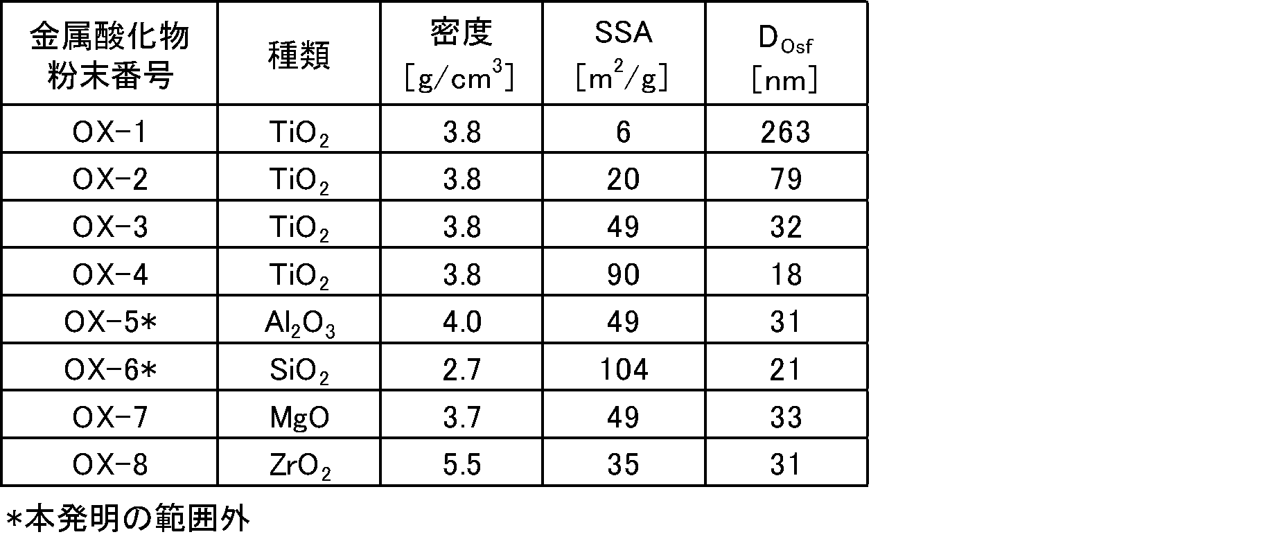

表1における金属粉末の粒径(DM10、DM50及びDM90)は、レーザー回折/散乱式粒度分布測定装置(堀場製作所製 LAシリーズ)を用いて測定した。測定溶媒は、エチルアルコールとイソプロピルアルコールの混合物を用いた。表1及び表2における金属粉末及び金属酸化物粉末のSSA(比表面積)は、N2ガスによるBET1点法によるSSA測定装置(マウンテック製 商品名マックソーブ(登録商標))を用いて測定した。表1及び表2における金属粉末及び金属酸化物粉末の密度は、乾式自動密度計(島津製作所製 商品名アキュピックシリーズ)を用いて測定した。表3における有機ビヒクルの密度は、比重カップ(安田精機製)を用いて測定した。
表1~表3に示した出発原料を、表4に示す組成比となるように調合し、三本ロールミルで分散処理を行なうことにより、導体ペーストP-1~P-15を得た。

[セラミック電子部品の作製]
導体ペーストP-1~P-15を用いて、スクリーン印刷により、グリーンシートの表面に内部導体層となる導体ペースト膜を形成した。導体ペースト膜が形成されたグリーンシートを所定枚数積層し、導体パターン膜が形成されていないグリーンシートで挟持した後、圧着して生の積層体を作製した。その後、還元雰囲気下、800~1000℃、60~180分間で焼成を行うことにより、セラミック絶縁体の内部に内部導体層が設けられたセラミック電子部品を得た。得られたセラミック電子部品に、導体ペーストの番号に対応したサンプル番号S-1~S-15を付した。
導体ペーストP-1~P-15を用いて、スクリーン印刷により、グリーンシートの表面に内部導体層となる導体ペースト膜を形成した。導体ペースト膜が形成されたグリーンシートを所定枚数積層し、導体パターン膜が形成されていないグリーンシートで挟持した後、圧着して生の積層体を作製した。その後、還元雰囲気下、800~1000℃、60~180分間で焼成を行うことにより、セラミック絶縁体の内部に内部導体層が設けられたセラミック電子部品を得た。得られたセラミック電子部品に、導体ペーストの番号に対応したサンプル番号S-1~S-15を付した。
[WDXによる元素分析]
機械研磨機を用いてセラミック電子部品S-1~S-15を研磨することにより、セラミック電子部品S-1~S-15の断面を露出させた。セラミック電子部品S-1~S-15の断面に対してフラットミリング処理及びカーボンコーティング処理を行った、WDX(波長分散型X線分光分析)測定装置(JEOL製 商品名JXA-8530F)を用いて元素分析を行った。WDXの測定条件を表5に示す。
機械研磨機を用いてセラミック電子部品S-1~S-15を研磨することにより、セラミック電子部品S-1~S-15の断面を露出させた。セラミック電子部品S-1~S-15の断面に対してフラットミリング処理及びカーボンコーティング処理を行った、WDX(波長分散型X線分光分析)測定装置(JEOL製 商品名JXA-8530F)を用いて元素分析を行った。WDXの測定条件を表5に示す。
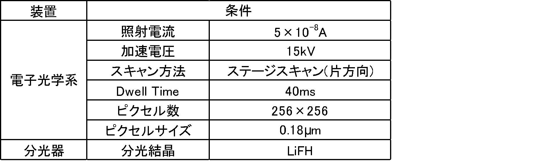
図4A~図4Dは、セラミック電子部品S-1~S-4の内部導体層付近の反射電子像及びTi元素のマッピング像である。図4A~図4Dにおいて、左側が反射電子像であり、右側がTi元素のマッピング像である。
図4A~図4Dに示すように、金属酸化物粉末としてTiO2粉末を含む導体ペーストP-1~P-4を用いて内部導体層を形成したセラミック電子部品S-1~S-4では、内部導体層の内部に、セラミック絶縁体と不連続な第1絶縁体領域が分散して存在するとともに、内部導体層の周囲に第2絶縁体領域が存在することが確認できる。さらに、図4Aから図4Dに向かってTiO2粉末のSSA(比表面積)が大きくなるほど、すなわち、比表面積換算粒径DOsfが小さくなるほど、第1絶縁体領域を構成する小領域のサイズが小さくなっていくことが確認できる。
図4A~図4Dに示すように、金属酸化物粉末としてTiO2粉末を含む導体ペーストP-1~P-4を用いて内部導体層を形成したセラミック電子部品S-1~S-4では、内部導体層の内部に、セラミック絶縁体と不連続な第1絶縁体領域が分散して存在するとともに、内部導体層の周囲に第2絶縁体領域が存在することが確認できる。さらに、図4Aから図4Dに向かってTiO2粉末のSSA(比表面積)が大きくなるほど、すなわち、比表面積換算粒径DOsfが小さくなるほど、第1絶縁体領域を構成する小領域のサイズが小さくなっていくことが確認できる。
図5A~図5Dは、セラミック電子部品S-1~S-4全体の反射電子像及びTi元素のマッピング像である。図5A~図5Dにおいて、左側が反射電子像であり、右側がTi元素のマッピング像である。
図5A~図5Dにおいても、図4A~図4Dと同様に、内部導体層の内部に、セラミック絶縁体と不連続な第1絶縁体領域が分散して存在するとともに、内部導体層の周囲に第2絶縁体領域が存在することが確認できる。一方、内部導体層と第2絶縁体領域との界面から20μm離れた領域では、第1絶縁体領域及び第2絶縁体領域に比べてTi元素の強度が小さいことが確認できる。したがって、セラミック絶縁体に含まれるTi元素の濃度は、第1絶縁体領域及び第2絶縁体領域におけるTi元素の濃度よりも低くなっていることが分かる。
図5A~図5Dにおいても、図4A~図4Dと同様に、内部導体層の内部に、セラミック絶縁体と不連続な第1絶縁体領域が分散して存在するとともに、内部導体層の周囲に第2絶縁体領域が存在することが確認できる。一方、内部導体層と第2絶縁体領域との界面から20μm離れた領域では、第1絶縁体領域及び第2絶縁体領域に比べてTi元素の強度が小さいことが確認できる。したがって、セラミック絶縁体に含まれるTi元素の濃度は、第1絶縁体領域及び第2絶縁体領域におけるTi元素の濃度よりも低くなっていることが分かる。
図示しないが、金属粉末であるCu粉末の粒径を変更した導体ペーストP-5~P-8を用いて内部導体層を形成したセラミック電子部品S-5~S-8、及び、金属酸化物粉末であるTiO2粉末の含有量を変更した導体ペーストP-13及びP-14を用いて内部導体層を形成したセラミック電子部品S-13及びS-14においても、セラミック電子部品S-3と同様、内部導体層の内部に、セラミック絶縁体と不連続な第1絶縁体領域が分散して存在するとともに、内部導体層の周囲に第2絶縁体領域が存在することが確認された。
図6Aは、セラミック電子部品S-11の内部導体層付近の反射電子像及びMg元素のマッピング層であり、図6Bは、セラミック電子部品S-12の内部導体層付近の反射電子像及びZr元素のマッピング像である。図6A及び図6Bにおいて、左側が反射電子像であり、右側がMg元素又はZr元素のマッピング像である。
図6Aに示すように、金属酸化物粉末としてMgO粉末を含む導体ペーストP-11を用いて内部導体層を形成したセラミック電子部品S-11、及び、図6Bに示すように、金属酸化物粉末としてZrO2粉末を含む導体ペーストP-12を用いて内部導体層を形成したセラミック電子部品S-12では、内部導体層の周囲の一部に第2絶縁体領域が存在しないものの、セラミック電子部品S-1~S-4と同様、内部導体層の内部に、セラミック絶縁体と不連続な第1絶縁体領域が分散して存在するとともに、内部導体層の周囲に第2絶縁体領域が存在することが確認できる。
図6Aに示すように、金属酸化物粉末としてMgO粉末を含む導体ペーストP-11を用いて内部導体層を形成したセラミック電子部品S-11、及び、図6Bに示すように、金属酸化物粉末としてZrO2粉末を含む導体ペーストP-12を用いて内部導体層を形成したセラミック電子部品S-12では、内部導体層の周囲の一部に第2絶縁体領域が存在しないものの、セラミック電子部品S-1~S-4と同様、内部導体層の内部に、セラミック絶縁体と不連続な第1絶縁体領域が分散して存在するとともに、内部導体層の周囲に第2絶縁体領域が存在することが確認できる。
一方、金属酸化物粉末としてAl2O3粉末を含む導体ペーストP-9を用いて内部導体層を形成したセラミック電子部品S-9、及び、金属酸化物粉末としてSiO2粉末を含む導体ペーストP-10を用いて内部導体層を形成したセラミック電子部品S-10では、第1絶縁体領域及び第2絶縁体領域の存在を確認することができなかった。これは、導体ペーストに含まれる金属酸化物粉末がセラミック絶縁体の原料粉末と反応してしまったためと考えられる。また、金属酸化物粉末を含まない導体ペーストP-15を用いて内部導体層を形成したセラミック電子部品S-15においても、第1絶縁体領域及び第2絶縁体領域の存在を確認することができなかった。
[内部導体層とセラミック絶縁体との間で生じる空隙の確認]
内部導体層とセラミック絶縁体との間で生じる空隙を確認するため、各セラミック電子部品に蛍光液を真空含浸させた後、乾燥機を用いて乾燥させた。その後、機械研磨機を用いて内部導体層を含む面が露出するまでセラミック電子部品を研磨した。Hg光源の顕微鏡を用いて研磨面を確認し、内部導体層とセラミック絶縁体との間に蛍光液が浸入しているかを確認した。
内部導体層とセラミック絶縁体との間で生じる空隙を確認するため、各セラミック電子部品に蛍光液を真空含浸させた後、乾燥機を用いて乾燥させた。その後、機械研磨機を用いて内部導体層を含む面が露出するまでセラミック電子部品を研磨した。Hg光源の顕微鏡を用いて研磨面を確認し、内部導体層とセラミック絶縁体との間に蛍光液が浸入しているかを確認した。
図7は、セラミック電子部品S-4の露出面の顕微鏡写真であり、図8は、セラミック電子部品S-15の露出面の顕微鏡写真である。
第1絶縁体領域及び第2絶縁体領域が存在するセラミック電子部品S-4では、図7に示すように蛍光液が浸入していないのに対し、第1絶縁体領域及び第2絶縁体領域が存在しないセラミック電子部品S-15では、図8に示すように蛍光液が浸入していることが確認できる。以上の結果から、第1絶縁体領域及び第2絶縁体領域を形成することにより、内部導体層とセラミック絶縁体との間で生じる空隙の形成が抑制されることが分かる。
第1絶縁体領域及び第2絶縁体領域が存在するセラミック電子部品S-4では、図7に示すように蛍光液が浸入していないのに対し、第1絶縁体領域及び第2絶縁体領域が存在しないセラミック電子部品S-15では、図8に示すように蛍光液が浸入していることが確認できる。以上の結果から、第1絶縁体領域及び第2絶縁体領域を形成することにより、内部導体層とセラミック絶縁体との間で生じる空隙の形成が抑制されることが分かる。
1 多層セラミック基板(セラミック電子部品)
2 積層セラミックコンデンサ(セラミック電子部品)
11,21,31 セラミック絶縁体
12,32 内部導体層
13,14 外部導体層
15 ビア導体
22a,22b,22c,22d,22e,22f 内層電極(内部導体層)
23a,23b 外部電極
41 第1絶縁体領域
42 第2絶縁体領域
43 内部導体層と第2絶縁体領域との界面から20μm離れた厚さ3μmの領域
44 内部導体層と第2絶縁体領域との界面
A 内部導体層の下面のうち、内部導体層の上面と接する部分
2 積層セラミックコンデンサ(セラミック電子部品)
11,21,31 セラミック絶縁体
12,32 内部導体層
13,14 外部導体層
15 ビア導体
22a,22b,22c,22d,22e,22f 内層電極(内部導体層)
23a,23b 外部電極
41 第1絶縁体領域
42 第2絶縁体領域
43 内部導体層と第2絶縁体領域との界面から20μm離れた厚さ3μmの領域
44 内部導体層と第2絶縁体領域との界面
A 内部導体層の下面のうち、内部導体層の上面と接する部分
Claims (11)
- セラミック絶縁体と、前記セラミック絶縁体の内部に設けられた内部導体層とを備えるセラミック電子部品であって、
前記内部導体層は、金属と、Ti、Mg及びZrからなる群より選択される少なくとも1種の金属元素を含む金属酸化物とを含み、
前記内部導体層の内部に、Ti、Mg及びZrからなる群より選択される少なくとも1種の金属元素を含み、前記セラミック絶縁体と不連続な第1絶縁体領域が分散して存在するとともに、
前記内部導体層の周囲に、前記第1絶縁体領域に含まれる前記金属元素と同じ金属元素を含む第2絶縁体領域が存在することを特徴とするセラミック電子部品。 - 前記セラミック絶縁体は、前記第1絶縁体領域及び前記第2絶縁体領域に含まれる前記金属元素と同じ金属元素を含む請求項1に記載のセラミック電子部品。
- 前記セラミック絶縁体に含まれる前記金属元素の濃度は、前記第1絶縁体領域における前記金属元素の濃度よりも低く、前記第2絶縁体領域における前記金属元素の濃度よりも低い請求項2に記載のセラミック電子部品。
- 前記内部導体層は、前記セラミック絶縁体の表面に露出している請求項1~3のいずれか1項に記載のセラミック電子部品。
- 前記セラミック絶縁体の表面に設けられた外部導体をさらに備え、
前記内部導体層は、前記外部導体によって被覆されている請求項1~3のいずれか1項に記載のセラミック電子部品。 - 前記内部導体層の下面のうち、前記内部導体層の上面と接する部分に生じる空隙の長さが100μm以下である請求項1~5のいずれか1項に記載のセラミック電子部品。
- 請求項1~6のいずれか1項に記載のセラミック電子部品の製造方法であって、
セラミック絶縁体の原料粉末を含む複数のグリーンシートを準備する工程と、
金属粉末と、金属酸化物粉末又は金属酸化物前駆体粉末と、有機ビヒクルとを含み、前記金属酸化物粉末又は前記金属酸化物前駆体粉末がTi、Mg及びZrからなる群より選択される少なくとも1種の金属元素を含む導体ペーストを準備する工程と、
前記グリーンシートの少なくとも1枚の主面に前記導体ペーストを塗布することによって、内部導体層となる導体ペースト膜を形成する工程と、
複数の前記グリーンシートが積層されるとともに、前記導体ペースト膜が前記グリーンシート間に形成された生の積層体を作製する工程と、
前記生の積層体を焼成する工程と、を備えることを特徴とするセラミック電子部品の製造方法。 - 前記金属酸化物粉末又は前記金属酸化物前駆体粉末の比表面積が、6m2/g以上90m2/g以下である請求項7に記載のセラミック電子部品の製造方法。
- 前記金属酸化物粉末又は金属酸化物前駆体粉末の比表面積換算粒径をDOsf[nm]、前記金属粉末の体積基準メディアン径をDM50[nm]としたとき、2.28≦DM50/DOsf≦105.5である請求項7又は8に記載のセラミック電子部品の製造方法。
- 前記金属粉末の焼結開始温度が、前記グリーンシートの焼結開始温度以下である請求項7~9のいずれか1項に記載のセラミック電子部品の製造方法。
- 前記セラミック絶縁体の原料粉末は、SiO2とAl2O3とBa化合物とを含む請求項7~10のいずれか1項に記載のセラミック電子部品の製造方法。
Priority Applications (3)
| Application Number | Priority Date | Filing Date | Title |
|---|---|---|---|
| JP2018514199A JP6544485B2 (ja) | 2016-04-28 | 2017-03-22 | セラミック電子部品及びセラミック電子部品の製造方法 |
| CN201780026163.9A CN109074956B (zh) | 2016-04-28 | 2017-03-22 | 陶瓷电子部件及陶瓷电子部件的制造方法 |
| US16/161,313 US11011306B2 (en) | 2016-04-28 | 2018-10-16 | Ceramic electronic component and method for producing ceramic electronic component |
Applications Claiming Priority (2)
| Application Number | Priority Date | Filing Date | Title |
|---|---|---|---|
| JP2016-091782 | 2016-04-28 | ||
| JP2016091782 | 2016-04-28 |
Related Child Applications (1)
| Application Number | Title | Priority Date | Filing Date |
|---|---|---|---|
| US16/161,313 Continuation US11011306B2 (en) | 2016-04-28 | 2018-10-16 | Ceramic electronic component and method for producing ceramic electronic component |
Publications (1)
| Publication Number | Publication Date |
|---|---|
| WO2017187848A1 true WO2017187848A1 (ja) | 2017-11-02 |
Family
ID=60160324
Family Applications (1)
| Application Number | Title | Priority Date | Filing Date |
|---|---|---|---|
| PCT/JP2017/011422 Ceased WO2017187848A1 (ja) | 2016-04-28 | 2017-03-22 | セラミック電子部品及びセラミック電子部品の製造方法 |
Country Status (4)
| Country | Link |
|---|---|
| US (1) | US11011306B2 (ja) |
| JP (1) | JP6544485B2 (ja) |
| CN (1) | CN109074956B (ja) |
| WO (1) | WO2017187848A1 (ja) |
Cited By (1)
| Publication number | Priority date | Publication date | Assignee | Title |
|---|---|---|---|---|
| JP2022134873A (ja) * | 2021-03-04 | 2022-09-15 | 太陽誘電株式会社 | セラミック電子部品およびその製造方法 |
Citations (2)
| Publication number | Priority date | Publication date | Assignee | Title |
|---|---|---|---|---|
| JP2013214698A (ja) * | 2012-04-02 | 2013-10-17 | Samsung Electro-Mechanics Co Ltd | 内部電極用導電性ペースト組成物及びそれを含む積層セラミック電子部品 |
| JP2015131982A (ja) * | 2014-01-09 | 2015-07-23 | 株式会社村田製作所 | 複合粉末とその製造方法およびそれを用いた導電性ペーストとそれを用いた積層セラミック電子部品 |
Family Cites Families (12)
| Publication number | Priority date | Publication date | Assignee | Title |
|---|---|---|---|---|
| JPS6014416A (ja) | 1983-07-05 | 1985-01-25 | Tdk Corp | 電子部品の製造方法 |
| JPH06290985A (ja) * | 1993-03-30 | 1994-10-18 | Taiyo Yuden Co Ltd | 内部電極ペースト |
| JP3243943B2 (ja) | 1994-08-25 | 2002-01-07 | 株式会社村田製作所 | セラミック電子部品の製造方法 |
| JP4776913B2 (ja) * | 2004-01-08 | 2011-09-21 | Tdk株式会社 | 積層型セラミックコンデンサ及びその製造方法 |
| JP4295179B2 (ja) * | 2004-08-31 | 2009-07-15 | Tdk株式会社 | 電子部品およびその製造方法 |
| US7158364B2 (en) * | 2005-03-01 | 2007-01-02 | Tdk Corporation | Multilayer ceramic capacitor and method of producing the same |
| JP5166049B2 (ja) * | 2008-01-21 | 2013-03-21 | 太陽誘電株式会社 | セラミック電子部品及びその製造方法 |
| CN101593622B (zh) * | 2009-06-30 | 2011-03-30 | 广东风华高新科技股份有限公司 | 一种mlcc铜内电极浆料 |
| KR101580350B1 (ko) * | 2012-06-04 | 2015-12-23 | 삼성전기주식회사 | 적층 세라믹 부품 |
| KR102089695B1 (ko) * | 2014-04-30 | 2020-03-16 | 삼성전기주식회사 | 적층 세라믹 전자부품 및 그 제조방법 |
| JP2015053502A (ja) * | 2014-10-23 | 2015-03-19 | 株式会社村田製作所 | 積層セラミックコンデンサ |
| JP6632808B2 (ja) * | 2015-03-30 | 2020-01-22 | 太陽誘電株式会社 | 積層セラミックコンデンサ |
-
2017
- 2017-03-22 CN CN201780026163.9A patent/CN109074956B/zh active Active
- 2017-03-22 WO PCT/JP2017/011422 patent/WO2017187848A1/ja not_active Ceased
- 2017-03-22 JP JP2018514199A patent/JP6544485B2/ja active Active
-
2018
- 2018-10-16 US US16/161,313 patent/US11011306B2/en active Active
Patent Citations (2)
| Publication number | Priority date | Publication date | Assignee | Title |
|---|---|---|---|---|
| JP2013214698A (ja) * | 2012-04-02 | 2013-10-17 | Samsung Electro-Mechanics Co Ltd | 内部電極用導電性ペースト組成物及びそれを含む積層セラミック電子部品 |
| JP2015131982A (ja) * | 2014-01-09 | 2015-07-23 | 株式会社村田製作所 | 複合粉末とその製造方法およびそれを用いた導電性ペーストとそれを用いた積層セラミック電子部品 |
Cited By (2)
| Publication number | Priority date | Publication date | Assignee | Title |
|---|---|---|---|---|
| JP2022134873A (ja) * | 2021-03-04 | 2022-09-15 | 太陽誘電株式会社 | セラミック電子部品およびその製造方法 |
| JP7721285B2 (ja) | 2021-03-04 | 2025-08-12 | 太陽誘電株式会社 | セラミック電子部品およびその製造方法 |
Also Published As
| Publication number | Publication date |
|---|---|
| US11011306B2 (en) | 2021-05-18 |
| US20190051458A1 (en) | 2019-02-14 |
| JP6544485B2 (ja) | 2019-07-17 |
| JPWO2017187848A1 (ja) | 2019-02-21 |
| CN109074956A (zh) | 2018-12-21 |
| CN109074956B (zh) | 2020-07-10 |
Similar Documents
| Publication | Publication Date | Title |
|---|---|---|
| US10090108B2 (en) | Conductive paste, electronic component, and method for manufacturing electronic component | |
| US10529486B2 (en) | Conductive paste for external electrode and method for manufacturing electronic component including the conductive paste for external electrode | |
| JP5904305B2 (ja) | 積層セラミックコンデンサおよびその製造方法 | |
| JP5617637B2 (ja) | セラミック積層部品とその製造方法 | |
| KR101577395B1 (ko) | 적층 세라믹 전자부품 및 그 제조방법 | |
| CN103827992B (zh) | 层叠型线圈部件 | |
| JP2020072263A (ja) | 積層セラミック電子部品とその製造方法 | |
| JP5324247B2 (ja) | 積層セラミックコンデンサ | |
| CN1841598B (zh) | 叠层陶瓷电子部件及其制造方法 | |
| JP2012182355A (ja) | 積層セラミックコンデンサ及び積層セラミックコンデンサの製造方法 | |
| CN109979734B (zh) | 线圈部件 | |
| JP6544485B2 (ja) | セラミック電子部品及びセラミック電子部品の製造方法 | |
| JP4826881B2 (ja) | 導電性ペースト、及び積層セラミック電子部品の製造方法、並びに積層セラミック電子部品 | |
| JP4333594B2 (ja) | 導電性ペースト及びセラミック電子部品 | |
| JP6369560B2 (ja) | セラミック配線基板およびセラミック配線基板の製造方法 | |
| WO2022163141A1 (ja) | 電子部品 | |
| JP2016192477A (ja) | 積層セラミック電子部品 | |
| JP4387150B2 (ja) | 積層セラミック電子部品およびその製造方法 | |
| JP2001143957A (ja) | 積層セラミックコンデンサおよびその製造方法 | |
| JP2003323817A (ja) | 導電性ペーストおよび積層セラミック電子部品 | |
| US20250002416A1 (en) | Laminated ceramic capacitor and method of manufacturing laminated ceramic capacitor | |
| JP5903913B2 (ja) | 積層電子部品 | |
| JP2000058375A (ja) | 積層セラミック電子部品及びその製造方法 | |
| JP3330817B2 (ja) | 多層セラミックス部品 | |
| JPH08148834A (ja) | コンデンサ内蔵ガラスセラミック多層配線基板 |
Legal Events
| Date | Code | Title | Description |
|---|---|---|---|
| ENP | Entry into the national phase |
Ref document number: 2018514199 Country of ref document: JP Kind code of ref document: A |
|
| NENP | Non-entry into the national phase |
Ref country code: DE |
|
| 121 | Ep: the epo has been informed by wipo that ep was designated in this application |
Ref document number: 17789137 Country of ref document: EP Kind code of ref document: A1 |
|
| 122 | Ep: pct application non-entry in european phase |
Ref document number: 17789137 Country of ref document: EP Kind code of ref document: A1 |