WO2017168992A1 - 半導体装置 - Google Patents
半導体装置 Download PDFInfo
- Publication number
- WO2017168992A1 WO2017168992A1 PCT/JP2017/002044 JP2017002044W WO2017168992A1 WO 2017168992 A1 WO2017168992 A1 WO 2017168992A1 JP 2017002044 W JP2017002044 W JP 2017002044W WO 2017168992 A1 WO2017168992 A1 WO 2017168992A1
- Authority
- WO
- WIPO (PCT)
- Prior art keywords
- insulating member
- conductor
- insulating
- base member
- layer
- Prior art date
- Legal status (The legal status is an assumption and is not a legal conclusion. Google has not performed a legal analysis and makes no representation as to the accuracy of the status listed.)
- Ceased
Links
Images



Classifications
-
- H—ELECTRICITY
- H10—SEMICONDUCTOR DEVICES; ELECTRIC SOLID-STATE DEVICES NOT OTHERWISE PROVIDED FOR
- H10W—GENERIC PACKAGES, INTERCONNECTIONS, CONNECTORS OR OTHER CONSTRUCTIONAL DETAILS OF DEVICES COVERED BY CLASS H10
- H10W40/00—Arrangements for thermal protection or thermal control
- H10W40/20—Arrangements for cooling
- H10W40/25—Arrangements for cooling characterised by their materials
- H10W40/255—Arrangements for cooling characterised by their materials having a laminate or multilayered structure, e.g. direct bond copper [DBC] ceramic substrates
-
- H—ELECTRICITY
- H02—GENERATION; CONVERSION OR DISTRIBUTION OF ELECTRIC POWER
- H02M—APPARATUS FOR CONVERSION BETWEEN AC AND AC, BETWEEN AC AND DC, OR BETWEEN DC AND DC, AND FOR USE WITH MAINS OR SIMILAR POWER SUPPLY SYSTEMS; CONVERSION OF DC OR AC INPUT POWER INTO SURGE OUTPUT POWER; CONTROL OR REGULATION THEREOF
- H02M7/00—Conversion of AC power input into DC power output; Conversion of DC power input into AC power output
- H02M7/42—Conversion of DC power input into AC power output without possibility of reversal
- H02M7/44—Conversion of DC power input into AC power output without possibility of reversal by static converters
- H02M7/48—Conversion of DC power input into AC power output without possibility of reversal by static converters using discharge tubes with control electrode or semiconductor devices with control electrode
-
- H—ELECTRICITY
- H10—SEMICONDUCTOR DEVICES; ELECTRIC SOLID-STATE DEVICES NOT OTHERWISE PROVIDED FOR
- H10W—GENERIC PACKAGES, INTERCONNECTIONS, CONNECTORS OR OTHER CONSTRUCTIONAL DETAILS OF DEVICES COVERED BY CLASS H10
- H10W44/00—Electrical arrangements for controlling or matching impedance
- H10W44/601—Capacitive arrangements
-
- H—ELECTRICITY
- H10—SEMICONDUCTOR DEVICES; ELECTRIC SOLID-STATE DEVICES NOT OTHERWISE PROVIDED FOR
- H10W—GENERIC PACKAGES, INTERCONNECTIONS, CONNECTORS OR OTHER CONSTRUCTIONAL DETAILS OF DEVICES COVERED BY CLASS H10
- H10W70/00—Package substrates; Interposers; Redistribution layers [RDL]
- H10W70/20—Conductive package substrates serving as an interconnection, e.g. metal plates
- H10W70/22—Conductive package substrates serving as an interconnection, e.g. metal plates having an heterogeneous or anisotropic structure
-
- H—ELECTRICITY
- H10—SEMICONDUCTOR DEVICES; ELECTRIC SOLID-STATE DEVICES NOT OTHERWISE PROVIDED FOR
- H10W—GENERIC PACKAGES, INTERCONNECTIONS, CONNECTORS OR OTHER CONSTRUCTIONAL DETAILS OF DEVICES COVERED BY CLASS H10
- H10W90/00—Package configurations
-
- H—ELECTRICITY
- H10—SEMICONDUCTOR DEVICES; ELECTRIC SOLID-STATE DEVICES NOT OTHERWISE PROVIDED FOR
- H10W—GENERIC PACKAGES, INTERCONNECTIONS, CONNECTORS OR OTHER CONSTRUCTIONAL DETAILS OF DEVICES COVERED BY CLASS H10
- H10W72/00—Interconnections or connectors in packages
-
- H—ELECTRICITY
- H10—SEMICONDUCTOR DEVICES; ELECTRIC SOLID-STATE DEVICES NOT OTHERWISE PROVIDED FOR
- H10W—GENERIC PACKAGES, INTERCONNECTIONS, CONNECTORS OR OTHER CONSTRUCTIONAL DETAILS OF DEVICES COVERED BY CLASS H10
- H10W72/00—Interconnections or connectors in packages
- H10W72/071—Connecting or disconnecting
- H10W72/076—Connecting or disconnecting of strap connectors
- H10W72/07651—Connecting or disconnecting of strap connectors characterised by changes in properties of the strap connectors during connecting
-
- H—ELECTRICITY
- H10—SEMICONDUCTOR DEVICES; ELECTRIC SOLID-STATE DEVICES NOT OTHERWISE PROVIDED FOR
- H10W—GENERIC PACKAGES, INTERCONNECTIONS, CONNECTORS OR OTHER CONSTRUCTIONAL DETAILS OF DEVICES COVERED BY CLASS H10
- H10W72/00—Interconnections or connectors in packages
- H10W72/60—Strap connectors, e.g. thick copper clips for grounding of power devices
-
- H—ELECTRICITY
- H10—SEMICONDUCTOR DEVICES; ELECTRIC SOLID-STATE DEVICES NOT OTHERWISE PROVIDED FOR
- H10W—GENERIC PACKAGES, INTERCONNECTIONS, CONNECTORS OR OTHER CONSTRUCTIONAL DETAILS OF DEVICES COVERED BY CLASS H10
- H10W72/00—Interconnections or connectors in packages
- H10W72/851—Dispositions of multiple connectors or interconnections
- H10W72/874—On different surfaces
- H10W72/884—Die-attach connectors and bond wires
-
- H—ELECTRICITY
- H10—SEMICONDUCTOR DEVICES; ELECTRIC SOLID-STATE DEVICES NOT OTHERWISE PROVIDED FOR
- H10W—GENERIC PACKAGES, INTERCONNECTIONS, CONNECTORS OR OTHER CONSTRUCTIONAL DETAILS OF DEVICES COVERED BY CLASS H10
- H10W90/00—Package configurations
- H10W90/701—Package configurations characterised by the relative positions of pads or connectors relative to package parts
- H10W90/731—Package configurations characterised by the relative positions of pads or connectors relative to package parts of die-attach connectors
- H10W90/734—Package configurations characterised by the relative positions of pads or connectors relative to package parts of die-attach connectors between a chip and a stacked insulating package substrate, interposer or RDL
-
- H—ELECTRICITY
- H10—SEMICONDUCTOR DEVICES; ELECTRIC SOLID-STATE DEVICES NOT OTHERWISE PROVIDED FOR
- H10W—GENERIC PACKAGES, INTERCONNECTIONS, CONNECTORS OR OTHER CONSTRUCTIONAL DETAILS OF DEVICES COVERED BY CLASS H10
- H10W90/00—Package configurations
- H10W90/701—Package configurations characterised by the relative positions of pads or connectors relative to package parts
- H10W90/751—Package configurations characterised by the relative positions of pads or connectors relative to package parts of bond wires
- H10W90/754—Package configurations characterised by the relative positions of pads or connectors relative to package parts of bond wires between a chip and a stacked insulating package substrate, interposer or RDL
Definitions
- the present invention relates to a semiconductor device.
- Some semiconductor devices perform a power conversion function for converting DC power to AC power or AC power to DC power.
- Patent Document 1 discloses one or more semiconductor chips, one or more conductors connected to the semiconductor chip, a ceramic substrate on which these are mounted, and a base plate on which the ceramic substrate is mounted. And an electric power conversion device including a radiator, an invention is disclosed in which an insulating plate is sandwiched between a base plate and a radiator, the radiator is grounded, and the dielectric strength is improved.
- Patent Documents 2 and 3 a lead frame in which a plurality of semiconductor elements are bonded to one surface, a first insulating layer disposed on the other surface of the lead frame, and the lead frame have a first insulation.
- An invention has been disclosed that includes a metal base plate connected to one surface via a layer and a second insulating layer disposed on the other surface of the metal base plate to improve insulation.
- a semiconductor device includes a semiconductor element, a conductor plate connected to the semiconductor element, a metal base member facing the conductor plate and constituting the exterior of the semiconductor device, and between the conductor plate and the base member. And an insulating member disposed between the first insulating layer and the conductor plate, the insulating member having a conductor layer sandwiched between the first insulating layer and the second insulating layer. And forming a capacitance circuit between the second insulating layer and the base member, and the base member is formed with a protruding portion that protrudes toward the insulating member at a contact portion between the insulating member and the base member.
- the length from the center of the layer to the peripheral edge of the insulating member including the conductor layer is longer than the length from the center of the conductive layer to the peripheral edge of the protruding portion of the base member.
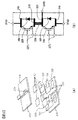
- FIGS. 2A and 2B are an external perspective view and an exploded perspective view of a power semiconductor module.
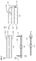
- A) (B) It is a disassembled perspective view which shows the assembly process of the internal wiring of a power semiconductor module, and a circuit diagram which shows an internal circuit.
- A) (B) (C) (D) It is sectional drawing which shows the assembly process of a power semiconductor module, sectional drawing which shows an internal structure, an expanded sectional view, and a bottom plan view.
- (A) (B) The figure explaining the voltage sharing effect of a power semiconductor module, It is a circuit diagram explaining the voltage sharing effect.
- (A) (B) (C) It is 2nd Embodiment, It is sectional drawing of a power semiconductor module, an expanded sectional view, and a bottom part top view.
- (A) (B) (C) (D) It is 3rd Embodiment and is a disassembled sectional view of a power semiconductor module, sectional drawing, an expanded sectional view, and a bottom part top view.
- (A) (B) (C) It is 4th Embodiment and is an exploded sectional view of a power semiconductor module, sectional drawing, and a bottom part top view.
- FIG. 1A is a perspective view showing the appearance of the power semiconductor module 300.
- FIG. 1B is an exploded perspective view showing an assembly process of the power semiconductor module 300.
- the sealing body 302 including the power semiconductor element is sandwiched by the insulating member 333 from both sides. Insulation between the terminals of the wiring led out from the power semiconductor element is ensured by the terminal mold material 317 to form the terminal mold 316.
- a state where the power semiconductor module 300 is assembled is shown in FIG.
- the sealing body 302 and the insulating member 333 are housed in the housing portion 306 of the case 304 and sealed with the second sealing resin 349.
- An O-ring groove 312 is formed on the outer periphery of the storage port of the storage unit 306.
- the power semiconductor element is fixed to a water channel casing (not shown) while an O-ring is attached to the O-ring groove 312 and the O-ring is compressed.
- the case 304 is provided with fins 305 on both sides to dissipate heat generated by the power semiconductor element.
- the fin 305 is formed of a member having electrical conductivity, for example, a composite material such as Cu, Cu alloy, Cu—C, or Cu—CuO, or a composite material such as Al, Al alloy, AlSiC, or Al—C. .
- a power module AC terminal 320D for connecting to an AC bus bar, a reactor, or the like constituting an inverter circuit (not shown), a power module DC positive terminal 315D for connecting to a capacitor or the like constituting the inverter circuit, and the power The module DC negative terminal 319D protrudes.
- an upper arm signal connection terminal 327U and a lower arm signal connection terminal 327L for controlling and protecting the power semiconductor element include a power module DC positive terminal 315D and a power module DC negative terminal 319D. Projecting in the same direction.
- FIG. 2A is an exploded perspective view showing an assembly process of internal wiring of the power semiconductor module 300, and a circuit diagram showing an equivalent circuit corresponding to FIG.
- the IGBT 328 and the diode 156 constituting the upper arm circuit, which is a power semiconductor element are bonded by a metal bonding material 331 so as to be sandwiched between the upper arm conductor plates 315 and 318.
- the IGBT 330 and the diode 166 constituting the lower arm circuit which is a power semiconductor element are joined by a metal joining material 331 so as to be sandwiched between the lower arm conductor plates 319 and 320.
- the upper arm circuit and the lower arm circuit are joined by a metal joining material 331 at the intermediate connection portion 329 to form an upper and lower arm series circuit.
- the upper arm circuit includes an IGBT 328 and a diode 156, and the power module DC positive terminal 315D is connected to the upper arm conductor plate 315.
- the lower arm circuit includes an IGBT 330 and a diode 166, and a power module DC negative terminal 319D is connected to the lower arm conductor plate 319.
- the upper arm conductor plate 318 and the lower arm conductor plate 320 are connected by an intermediate connection portion 329.
- the lower arm conductor plate 320 is connected to the power module AC terminal 320D.
- the gate electrode of the IGBT 328 of the upper arm circuit is connected to one of the upper arm signal connection terminals 327U, and the emitter electrode of the IGBT 328 of the upper arm circuit is connected to the other one of the upper arm signal connection terminals 327U.
- the gate electrode of the IGBT 330 of the lower arm circuit is connected to one of the lower arm signal connection terminals 327L, and the emitter electrode of the IGBT 330 of the lower arm circuit is connected to the other one of the lower arm signal connection terminals 327L.
- the IGBTs 328 and 330, the diodes 156 and 166, and the conductor plates 315, 318, 319, and 320 are sealed with a sealing resin material to form a sealing body 302 shown in FIG.
- sealing resin used for the sealing body 302 for example, a resin based on a novolac-based, polyfunctional, or biphenyl-based epoxy resin can be used, and ceramics and gels such as SiO2, Al2O3, AlN, and BN, Rubber or the like is included to make the thermal expansion coefficient close to the conductor plates 315, 318, 319, and 320.
- ceramics and gels such as SiO2, Al2O3, AlN, and BN, Rubber or the like is included to make the thermal expansion coefficient close to the conductor plates 315, 318, 319, and 320.
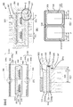
- FIG. 3A is a cross-sectional view showing an assembly process of the power semiconductor module 300, and is a cross-sectional view taken along the line AA in FIG. 1B.
- FIG. 3B is a cross-sectional view showing the internal structure of the power semiconductor module 300, and is a cross-sectional view taken along the line BB in FIG.
- FIG. 3C is a cross-sectional view showing a detailed structure of the power semiconductor module 300, and is an enlarged cross-sectional view of a portion C of FIG. 3B.
- FIG. 3D is a plan view of the power semiconductor module 300, and is a bottom plan view seen from the direction D in FIG. 3B.
- IGBTs 328 and 330 are joined to conductor plates 315, 318, 319, and 320 via a metal joining material 331 to constitute a sealing body 302.
- An insulating member 333 is provided outside the sealing body 302.
- the insulating member 333 includes a conductor layer 334 provided by being stacked between the first insulating layer 335a and the second insulating layer 335b.
- the lower conductor layer 334 in FIG. 3A is divided by the slit portion 339 so as to correspond to the gap between the conductor plate 315 and the conductor plate 320.
- the upper conductor layer 334 is divided by the slit portion 339 so as to correspond to the gap between the conductor plate 318 and the conductor plate 319.
- the power semiconductor module 300 is configured by sealing the sealing body 302 between the base members 307 of the case 304 with the insulating member 333 interposed therebetween.
- the case 304 including the base member 307 constitutes the exterior of the power semiconductor module 300 and is made of metal.
- the conductor layer 334 of the insulating member 333 faces the conductor plates 315, 318, 319, and 320, respectively.
- the remaining space of the case 304 is filled with the second sealing resin 349 to suppress moisture absorption and thermal stress of the insulating member 333.
- the sealing resin used for the second sealing resin 349 for example, a resin based on a novolac-based, polyfunctional, or biphenyl-based epoxy resin can be used, and ceramics such as SiO2, Al2O3, AlN, BN, etc. Gel, rubber or the like is included, and the thermal expansion coefficient is brought close to the case 304. As a result, the difference in thermal expansion coefficient between the members can be reduced, and the thermal stress generated as the temperature rises in the use environment is reduced, so that the life of the power semiconductor module 300 can be extended.
- metal bonding material 33 for example, a Sn brazing material (solder) based on Sn alloy, a hard brazing material such as an Al alloy or a Cu alloy, or a metal sintered material using metal nanoparticles or microparticles is used.
- FIG. 3C is an enlarged cross-sectional view of a portion C in FIG.
- the base member 307 is formed with a table-like protruding portion 307 a that protrudes toward the insulating member 333 at the contact portion between the insulating member 333 and the base member 307.
- a length L2 from the center P of the conductor layer 334 to the peripheral edge of the insulating member 333 is longer than a length L1 from the center P of the conductor layer 334 to the peripheral edge of the protruding portion 307a of the base member 307.
- the base end surface 308 at the peripheral portion of the protruding portion 307 a is located on the inner side of the insulating member end surface 336 at the peripheral portion of the insulating member 333. Furthermore, the insulating member end surface 336 of the insulating member 333 and the conductor layer end surface 344 of the conductor layer 334 form end surfaces at the same position. As described above, the base end surface 308 at the peripheral edge of the protruding portion 307a is located on the inner side of the insulating member end surface 336 at the peripheral edge of the insulating member 333, so that the gap between the conductor layer 334 and the base member 307 is reached. Insulation distance is secured.
- the positional relationship among the base end surface 308, the insulating member end surface 336, the conductor layer end surface 344, and the conductor plates 315, 318, 319, and 320 is shown in FIG. As shown in this figure, the base end surface 308 is located on the inner side of the insulating member end surface 336, and the conductor plates 315, 318, 319, and 320 are disposed on the inner side of the conductor layer end surface 344.
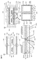
- FIG. 4 (A) is an exploded cross-sectional view for explaining the crimping method of the insulating member 333.
- the insulating member 333 is formed by laminating a conductor layer 334 with a first insulating layer 335a and a second insulating layer 335b made of an insulating material, and thermocompression bonding under a vacuum state. Molded.
- both ends are cut off with a die M or the like as shown in FIG.
- the conductor layer 334 is divided by the slit portion 339.
- FIG. 4C the shape and dimensions of the insulating member 333 are formed and finished.
- FIG. 4D A detailed enlarged view of the peripheral portion E of the insulating member end surface 336 of the insulating member 333 is shown in FIG.
- the insulating member end surface 336 may have cracks 340 and burrs 341 due to being cut off by the punching die M or the like. In this case, when the conductor layer 334 comes into contact with the base member 307, a short circuit occurs and the insulation performance is degraded.
- the conductor layer end surface 344 of the conductor layer 334 is disposed on the same plane as the insulating member end surface 336.
- the base end surface 308 of the peripheral part of the protrusion part 307a is located inside the insulating member end surface 336 of the peripheral part of the insulating member 333. Therefore, an insulation distance can be ensured between the conductor layer 334 and the base member 307, and insulation performance can be improved.
- FIG. 5A is an enlarged cross-sectional view for explaining the voltage sharing effect of the power semiconductor module 300.
- FIG. 5B is a circuit diagram illustrating the voltage sharing effect of the power semiconductor module 300.
- a surge voltage during switching operation is added to the DC voltage of the inverter system, and the maximum voltage during operation reaches the vicinity of the withstand voltage of the power semiconductor element.
- a value substantially close to this voltage value is applied between the insulating member 333 and the case 304.
- the applied voltage is shared by the conductor layer 334, and the voltage applied to the first insulating layer 335a and the second insulating layer 335b can be reduced.
- the electrostatic capacitances 338 thereof are equal, and the first insulating layer 335a and the second insulating layer 335b. Can be reduced to half of the voltage applied to the insulating member 333. Accordingly, when the void 337 exists inside the first insulating layer 335a and the second insulating layer 335b, the voltage value applied to the void 337 can be reduced, so that the discharge voltage of the void 337 is improved and the insulating member 333 is increased. The discharge start voltage can be improved. If this state is shown by an equivalent circuit, as shown in FIG. 5B, when the case 304 is at the ground potential, there is equivalently electrostatic between each conductor plate 315, 318, 319, 320 and the ground potential. A circuit is formed by connecting two capacitors 338 in series.
- FIGS. 6A, 6B, and 6C are diagrams illustrating the second embodiment.
- 6A is a cross-sectional view of the power semiconductor module 300
- FIG. 6B is an enlarged cross-sectional view of a portion F in FIG. 6A
- FIG. 6C is a cross-sectional view of FIG. It is the bottom part top view seen from.
- a base recess 309 is provided on the end surface of the base member 307. This is different from the first embodiment shown in FIG. 3B, and the other parts have the same configuration.
- the base recess 309 By providing the base recess 309, the base recess end surface 309 a of the base member 307 is positioned on the inner side of the insulating member end surface 336 as shown in FIG. 6B.
- the base member 307 is formed with a base-like protruding portion 307 a that protrudes toward the insulating member 333 at the contact portion between the insulating member 333 and the base member 307.
- FIG. 6C shows the positional relationship between the base recess end surface 309a, the insulating member end surface 336, and the conductor plates 315, 318, 319, and 320.
- the length L3 from the center P of the conductor layer 334 to the peripheral edge of the insulating member 333 is the length from the center P of the conductor layer 334 to the base recess end surface 309a of the base member 307, that is, the protrusion from the center P of the conductor layer 334 It is formed longer than the length L4 to the periphery of 307a.
- the positions of the insulating member end surface 336 and the conductor layer end surface 344 are larger to the outside than the base recess end surface 309a, whereby an insulation distance can be secured and the insulation performance can be improved.
- the conductor plates 315, 318, 319, and 320 are disposed on the inner side of the insulating member end surface 336.
- FIGS. 7A, 7B, 7C, and 7D are diagrams showing the third embodiment.
- 7A is an exploded cross-sectional view of the power semiconductor module 300
- FIG. 7B is a cross-sectional view of the power semiconductor module 300
- FIG. 7C is an enlarged cross-sectional view of a portion G in FIG. 7B
- 7 (D) is a bottom plan view of FIG. 7 (B) viewed from the D direction.
- the insulating member 333 is divided into the same number as the conductor plates 315, 318, 319, 320, and the plurality of divided insulating members 333 are divided into a plurality of conductor plates 315, 318, 319 and 320 are arranged opposite to each other.
- a recess 310 is formed in the base member 307 so as to face a gap position where a plurality of divided insulating members 333 are adjacent.
- Other configurations are the same as those of the second embodiment. As shown in FIG.
- the conductor layer end surface 344 and the insulating member end surface 336 are on the same plane, and the concave end surface 310a of the concave portion 310 is located on the inner side of the insulating member end surface 336 of the insulating member 333.
- the recess 310 forms two base-like protrusions 307 a that protrude toward the insulating member 333 at the contact portion between the insulating member 333 and the base member 307.
- the length L6 from the center P of the conductor layer 334 to the peripheral edge of the insulating member 333 is the length from the center P of the conductor layer 334 to the peripheral edge of the protruding portion 307a of the base member 307. It is formed longer than the length L5. According to the present embodiment, it is possible to secure an insulation distance and improve insulation performance, and by dividing the insulation member 333, the slit portion 339 shown in FIG. It can be simplified.
- FIGS. 8A, 8B, and 8C are diagrams illustrating the fourth embodiment.
- 8A is an exploded sectional view of the power semiconductor module 300
- FIG. 8B is a sectional view of the power semiconductor module 300
- FIG. 8C is a bottom portion of FIG. 8B viewed from the D direction. It is a top view.
- the conductor layer 334 of the insulating member 333 is not provided with the slit portion 339 shown in FIG. This is different from the first embodiment shown in FIG. 3A, and other parts have the same configuration.
- 8B shows the case where the shape of the base member 307 is the same as that of the first embodiment, the configuration may be the same as that of the second embodiment.
- the base member 307 is formed with a table-like protruding portion 307 a that protrudes toward the insulating member 333 at the contact portion between the insulating member 333 and the base member 307.
- the length L8 from the center P of the conductor layer 334 to the insulating member end surface 336 that is the peripheral edge of the insulating member 333 is the end face of the protrusion 307a that is the peripheral edge of the protrusion 307a of the base member 307 from the center P of the conductor layer 334. It is longer than the length L7 up to 308. According to this embodiment, since there is no slit 339 in the conductor layer 334 of the insulating member 333, the manufacturing process can be simplified.
- FIG. 9 is an exploded cross-sectional view of a power semiconductor module 300 showing the fifth embodiment.
- the conductor layer 334 of the insulating member 333 is not provided with the slit portion 339 illustrated in FIG. Further, the conductor layer 334 of the insulating member 333 is laminated in two layers with an insulating layer interposed therebetween. Other parts are the same as those in the first embodiment.
- the shape of the base member 307 may be the shape shown in FIG. 3B shown in the first embodiment, or the shape shown in FIG. 6A shown in the second embodiment. According to this embodiment, since the conductor layer 334 is laminated
- FIG. 10 is an exploded sectional view showing the sixth embodiment.
- the conductor layer 334 of the insulating member 333 is provided in a portion facing the AC potential conductor plates 318 and 320, and is not provided in a portion facing the conductor plates 319 and 315.
- the base member 307 is formed with a table-like protruding portion 307 a that protrudes toward the insulating member 333 at the contact portion between the insulating member 333 and the base member 307.
- the shape of the base member 307 may be the shape shown in FIG. 6A shown in the second embodiment.
- the relationship between the insulating member 333 and the base member 307 facing the AC potential conductor plates 318 and 320 is as follows.
- the length from the center of the conductor layer 334 to the peripheral edge portion of the insulating member 333 is longer than the length from the center of the conductor layer 334 to the peripheral edge portion of the protruding portion 307 a of the base member 307.
- Other parts are the same as those in the first embodiment. According to this embodiment, since the conductor layer 334 is provided at a place where a withstand voltage is required, the insulation performance is improved and the manufacturing process can be simplified.
- FIGS. 11A and 11B are power semiconductor modules 300 showing the structure of the seventh embodiment.
- FIG. 11A is an exploded cross-sectional view and FIG. 11B is a bottom plan view.
- the insulating member 333 is divided and arranged so as to face the conductor plates 315, 318, 319, and 320, respectively, and the conductor layer 334 of the insulating member 333 has an AC potential. It is provided in a portion facing the conductor plates 318 and 320 and is not provided in a portion facing the conductor plates 319 and 315.
- the base member 307 is provided with a recess 310 at the center of the base member 307.
- the base member 307 is formed with a table-like protruding portion 307 a that protrudes toward the insulating member 333 at the contact portion between the insulating member 333 and the base member 307.
- the shape of the base member 307 may be the shape shown in FIG. 6A shown in the second embodiment.
- FIG. 11B shows the relationship between the insulating member 333 facing the AC potential conductor plates 318 and 320 and the base member 307. That is, the length L10 from the center P of the conductor layer 334 to the peripheral edge of the insulating member 333 is longer than the length L9 from the center of the conductor layer 334 to the peripheral edge of the protruding portion 307a of the base member 307. According to this embodiment, since the conductor layer 334 is provided at a place where a withstand voltage is required, the insulation performance is improved and the manufacturing process can be simplified.
- the power semiconductor module 300 is opposed to a semiconductor element (IGBT 328, a diode 156), conductor plates 315, 318, 319, and 320 connected to the semiconductor element, and conductor plates 315, 318, 319, and 320.
- a metal base member 307 constituting the exterior of the semiconductor module 300, and an insulating member 333 disposed between the conductor plates 315, 318, 319, 320 and the base member 307.
- a conductive layer 334 is sandwiched between the first insulating layer 335a and the second insulating layer 335b, and a capacitance circuit is formed between the first insulating layer 335a and the conductive plates 315, 318, 319, 320, A capacitance circuit is formed between the second insulating layer 335b and the base member 307, and the base member 307 includes the insulating member 333, the base member 307, and the like.
- a trapezoidal protrusion 307 a that protrudes toward the insulating member 333 is formed at the contact portion, and the length from the center of the conductor layer 334 to the peripheral edge of the insulating member 333 including the conductor layer 334 is based on the base of the conductor layer 334.
- the member 307 is formed to be longer than the length to the peripheral edge of the protrusion 307a.
- the present invention is not limited to the above-described embodiment, and may be configured by combining the above-described embodiments.
- other forms conceivable within the scope of the technical idea of the present invention are also included in the scope of the present invention as long as the characteristics of the present invention are not impaired.
Landscapes
- Engineering & Computer Science (AREA)
- Power Engineering (AREA)
- Inverter Devices (AREA)
- Cooling Or The Like Of Semiconductors Or Solid State Devices (AREA)
Abstract
絶縁の信頼性が低くなるという課題がある。 導体層334の中心Pから絶縁部材333の周縁部までの長さL2は、導体層334の中心Pからベース部材307の突出部307aの周縁部までの長さL1より長く形成されている。換言すると、突出部307aの周縁部のベース端面308は、絶縁部材333の周縁部の絶縁部材端面336よりも内部側に位置している。更に、絶縁部材333の絶縁部材端面336と導体層の導体層端面344は同一位置で端面を形成している。このように、突出部307aの周縁部のベース端面308が、絶縁部材333の周縁部の絶縁部材端面336よりも内部側に位置していることで絶縁距離を確保できる。
Description
本発明は、半導体装置に関する。
半導体装置として、直流電力を交流電力に、または交流電力を直流電力に変換するための電力変換機能を行うものがある。
このような半導体装置として、特許文献1には、1つまたは複数の半導体チップと、この半導体チップと接続する1つまたは複数の導体と、これらを搭載するセラミック基板と、セラミック基板を搭載したベースプレートと、放熱器とから構成される電力変換装置において、ベースプレートと放熱器の間に絶縁プレートを挟み、放熱器を接地して、絶縁耐力を向上する発明が開示されている。また、特許文献2、3には、複数の半導体素子が一方の面に接合されたリードフレームと、リードフレームの他方の面に配置された第1の絶縁層と、リードフレームが第1の絶縁層を介して一方の面に接続された金属ベース板と、金属ベース板の他方の面に配置された第2の絶縁層と、を備え、絶縁性を向上する発明が開示されている。
特許文献2、3に記載される半導体装置は、第2の絶縁層が金属ベース板の外部に露出されて配置されるため、吸湿や熱応力によって第1の絶縁層に比べて絶縁の信頼性が低くなるという課題がある。
本発明による半導体装置は、半導体素子と、半導体素子に接続される導体板と、導体板と対向し、半導体装置の外装を構成する金属製のベース部材と、導体板とベース部材との間に配置される絶縁部材と、を備え、絶縁部材は、第1絶縁層と第2絶縁層との間に導体層を挟んで構成され、第1絶縁層と導体板との間で静電容量回路を形成し、第2絶縁層とベース部材との間で静電容量回路を形成し、ベース部材は、絶縁部材とベース部材との接触部分において絶縁部材側に突出する突出部が形成され、導体層の中心から導体層を含む絶縁部材の周縁部までの長さは、導体層の中心からベース部材の突出部の周縁部までの長さより長く形成される。
本発明によれば、絶縁性を確実に確保できる半導体装置を提供できる。
(第1の実施形態)
以下、本発明の半導体装置をパワー半導体モジュールに適用した例で説明する。
図1(A)は、パワー半導体モジュール300の外観を示す斜視図である。図1(B)は、パワー半導体モジュール300の組立て工程を示す分解斜視図である。
以下、本発明の半導体装置をパワー半導体モジュールに適用した例で説明する。
図1(A)は、パワー半導体モジュール300の外観を示す斜視図である。図1(B)は、パワー半導体モジュール300の組立て工程を示す分解斜視図である。
図1(B)に示すように、パワー半導体素子を内包した封止体302は、両面から絶縁部材333によって挟持される。パワー半導体素子より導出される配線の端子間の絶縁は端子モールド材317によって確保され、端子モールド316を形成する。パワー半導体モジュール300を組み立てた状態を図1(A)に示す。封止体302と絶縁部材333は、ケース304の収納部306に収納され、第2封止樹脂349によって封止される。収納部306の収納口の外周部にはOリング溝312が形成される。パワー半導体素子は、Oリング溝312にOリングを取り付け、このOリングを圧縮しながら図示省略した水路筐体に固定される。ケース304には両面にフィン305が設けられ、パワー半導体素子の発熱を放熱する。フィン305は、電気伝導性を有する部材、例えばCu、Cu合金、Cu-C、Cu-CuOなどの複合材、あるいはAl、Al合金、AlSiC、Al-Cなどの複合材などから形成されている。パワー半導体モジュール300から、図示省略したインバータ回路を構成する交流バスバーやリアクトル等と接続するためのパワーモジュール交流端子320D、インバータ回路を構成するキャパシタ等と接続するためパワーモジュール直流正極端子315D、及びパワーモジュール直流負極端子319Dが突出している。また、パワー半導体モジュール300から、パワー半導体素子の制御と保護のための上アーム用信号接続端子327Uと下アーム用信号接続端子327Lが、パワーモジュール直流正極端子315D、及びパワーモジュール直流負極端子319Dと同方向に突出している。
図2(A)は、パワー半導体モジュール300の内部配線の組み立て工程を示す分解斜視図、図2(A)に対応する等価回路を示す回路図である。
パワー半導体素子である上アーム回路を構成するIGBT328とダイオード156は、図2(A)に示すように、上アーム導体板315、318で挟まれる様に金属接合材331によって接合される。同様に、パワー半導体素子である下アーム回路を構成するIGBT330とダイオード166は下アーム導体板319、320で挟まれる様に金属接合材331によって接合される。上アーム回路と下アーム回路は、中間接続部329で金属接合材331によって接合され、上下アーム直列回路を形成している。
パワー半導体素子である上アーム回路を構成するIGBT328とダイオード156は、図2(A)に示すように、上アーム導体板315、318で挟まれる様に金属接合材331によって接合される。同様に、パワー半導体素子である下アーム回路を構成するIGBT330とダイオード166は下アーム導体板319、320で挟まれる様に金属接合材331によって接合される。上アーム回路と下アーム回路は、中間接続部329で金属接合材331によって接合され、上下アーム直列回路を形成している。
図2(B)に示すように、上アーム回路は、IGBT328とダイオード156とを備え、上アーム導体板315にパワーモジュール直流正極端子315Dが接続される。また下アーム回路は、IGBT330とダイオード166とを備え、下アーム導体板319にパワーモジュール直流負極端子319Dが接続される。上アーム導体板318と下アーム導体板320は、中間接続部329で接続される。また、下アーム導体板320はパワーモジュール交流端子320Dに接続される。上アーム回路のIGBT328のゲート電極は、上アーム用信号接続端子327Uの一つに、上アーム回路のIGBT328のエミッタ電極は、上アーム用信号接続端子327Uの他の一つに接続される。下アーム回路のIGBT330のゲート電極は、下アーム用信号接続端子327Lの一つに、下アーム回路のIGBT330のエミッタ電極は、下アーム用信号接続端子327Lの他の一つに接続される。IGBT328、330とダイオード156、166と、導体板315、318、319、320は、封止樹脂材によって封止されて、図1(B)に示す封止体302を形成する。
封止体302に用いる封止樹脂としては、例えばノボラック系、多官能系、ビフェニル系のエポキシ樹脂系を基とした樹脂を用いることができ、SiO2、Al2O3、AlN、BNなどのセラミックスやゲル、ゴムなどを含有させ、熱膨張係数を導体板315、318、319、320に近づける。これにより、部材間の熱膨張係数差を低減でき、使用環境時の温度上昇にともない発生する熱応力が低下するため、パワー半導体モジュール300の寿命をのばすことが可能となる。
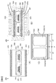
図3(A)は、パワー半導体モジュール300の組立て工程を示す断面図であり、図1(B)のA-A断面図である。図3(B)は、パワー半導体モジュール300の内部構造を示す断面図であり、図1(A)のB-B断面図である。 図3(C)は、パワー半導体モジュール300の詳細構造を示す断面図であり、図3(B)のC部の拡大断面図である。図3(D)は、パワー半導体モジュール300の平面図であり、図3(B)のD方向から見た底部平面図である。
図3(A)に示すように、IGBT328、330が金属接合材331を介して導体板315、318、319、320に接合され、封止体302を構成する。封止体302の外側には、絶縁部材333が設けられている。絶縁部材333は、第1絶縁層335aと第2絶縁層335bとの間に積層して設けられた導体層334を有する。図3(A)の図示下側の導体層334は、導体板315と導体板320との間の隙間と対応する様にスリット部339によって分割されている。同様に、図示上側の導体層334は、導体板318と導体板319との間の隙間と対応する様にスリット部339によって分割されている。
図3(B)に示すように、封止体302を絶縁部材333を介してケース304のベース部材307の間に封止してパワー半導体モジュール300を構成する。ベース部材307を含むケース304は、パワー半導体モジュール300の外装を構成し、金属製である。このように、絶縁部材333の導体層334は、それぞれ導体板315、318、319、320に対向している。また、ケース304の余空隙は第2封止樹脂349が充填され、絶縁部材333の吸湿と熱応力を抑制する。
第2封止樹脂349に用いる封止樹脂としては、例えばノボラック系、多官能系、ビフェニル系のエポキシ樹脂系を基とした樹脂を用いることができ、SiO2、Al2O3、AlN、BNなどのセラミックスやゲル、ゴムなどを含有させ、熱膨張係数をケース304に近づける。これにより、部材間の熱膨張係数差を低減でき、使用環境時の温度上昇にともない発生する熱応力が低下するため、パワー半導体モジュール300の寿命をのばすことが可能となる。金属接合材331は、例えばSn合金系の軟ろう材(はんだ)やAl合金、Cu合金等の硬ろう材や金属のナノ粒子、マイクロ粒子を用いた金属焼結材を用いる。
図3(C)は、図3(B)のC部の拡大断面図である。ベース部材307は、絶縁部材333とベース部材307との接触部分において絶縁部材333側に突出する台状の突出部307aが形成されている。そして導体層334の中心Pから絶縁部材333の周縁部までの長さL2は、導体層334の中心Pからベース部材307の突出部307aの周縁部までの長さL1より長く形成されている。換言すると、突出部307aの周縁部のベース端面308は、絶縁部材333の周縁部の絶縁部材端面336よりも内部側に位置している。更に、絶縁部材333の絶縁部材端面336と導体層334の導体層端面344は同一位置で端面を形成している。このように、突出部307aの周縁部のベース端面308が、絶縁部材333の周縁部の絶縁部材端面336よりも内部側に位置していることで、導体層334とベース部材307との間の絶縁距離を確保している。ベース端面308、絶縁部材端面336、導体層端面344及び導体板315、318、319、320の位置関係を、図3(D)に示す。この図に示すように、ベース端面308が、絶縁部材端面336よりも内部側に位置しており、導体板315、318、319、320は、導体層端面344の内部側に配置される。
図4(A)は、絶縁部材333の圧着工法を説明する分解断面図である。絶縁部材333は、図4(A)に示すように、絶縁材料で構成される第1絶縁層335aと第2絶縁層335bで導体層334を挟んで積層し、真空状態の下で熱圧着により成形される。
絶縁部材333を熱圧着して成形した後に、図4(B)に示すように、両端を抜き金型M等で切り落とす。なお、導体層334は、スリット部339によって分割されている。そして、図4(C)に示すように、絶縁部材333の形と寸法を成形して仕上げる。絶縁部材333の絶縁部材端面336の周辺部Eの詳細拡大図を図4(D)に示す。絶縁部材端面336は、図4(D)に示すように、抜き金型M等で切り落としたためにクラック340やバリ341が発生しているおそれがある。この場合、導体層334がベース部材307と接触すると短絡して絶縁性能が低下する。しかしながら、本実施形態では、図3(C)に示したように、導体層334の導体層端面344は、絶縁部材端面336と同一面上に配置している。そして、突出部307aの周縁部のベース端面308が、絶縁部材333の周縁部の絶縁部材端面336よりも内部側に位置している。そのため、導体層334とベース部材307との間で絶縁距離を確保でき、絶縁性能を向上させることができる。
図5(A)は、パワー半導体モジュール300の電圧分担効果を説明する拡大断面図である。図5(B)は、パワー半導体モジュール300の電圧分担効果を説明した回路図である。パワー半導体モジュール300の動作時には、インバータシステムの直流電圧にスイッチング動作時のサージ電圧が加わり、動作時の最高電圧はパワー半導体素子の耐圧近傍まで到達する。このとき、絶縁部材333とケース304の間には、略この電圧値に近い値が印加される。このとき、導体層334によってこの印加電圧が分担され、第1絶縁層335a及び第2絶縁層335bに印加される電圧を低減できる。例えば、導体層334の両面側の第1絶縁層335a、第2絶縁層335bの厚みと誘電率が等しい場合、両者の静電容量338が等しくなり、第1絶縁層335a及び第2絶縁層335bに印加される電圧が、絶縁部材333に印加される電圧の半分に低減できる。これにより、第1絶縁層335a、第2絶縁層335bの内部にボイド337が存在する場合、ボイド337に引加される電圧値も低減できるため、ボイド337の放電電圧を向上し、絶縁部材333の放電開始電圧を向上することができる。この状態を等価回路で示せば、図5(B)のように、ケース304が接地電位にあるとき、各導体板315、318、319、320と接地電位の間には、等価的に静電容量338が2直列されて形成された回路となる。
(第2の実施形態)
図6(A)(B)(C)は、第2の実施形態を示す図である。図6(A)は、パワー半導体モジュール300の断面図、図6(B)は、図6(A)のF部の拡大断面図、図6(C)は、図6(A)をD方向から見た底部平面図である。
図6(A)(B)(C)は、第2の実施形態を示す図である。図6(A)は、パワー半導体モジュール300の断面図、図6(B)は、図6(A)のF部の拡大断面図、図6(C)は、図6(A)をD方向から見た底部平面図である。
本実施形態では、図6(B)に示すように、ベース部材307の端面にベース凹部309を設ける。この点が図3(B)に示す第1の実施形態とは異なり、その他の部分は同様の構成である。ベース凹部309を設けることにより、図6(B)に示すように、ベース部材307のベース凹部端面309aが絶縁部材端面336よりも内部側に位置する。換言すると、ベース凹部309を設けたことにより、ベース部材307は、絶縁部材333とベース部材307との接触部分において絶縁部材333側に突出する台状の突出部307aが形成される。
図6(C)に、ベース凹部端面309a、絶縁部材端面336、及び導体板315、318、319、320の位置関係を示す。導体層334の中心Pから絶縁部材333の周縁部までの長さL3は、導体層334の中心Pからベース部材307のベース凹部端面309aまでの長さ、すなわち導体層334の中心Pから突出部307aの周縁部までの長さL4より長く形成されている。換言すれば、ベース凹部端面309aよりも絶縁部材端面336と導体層の端面344の位置が外側に大きく、これにより、絶縁距離を確保でき、絶縁性能を向上させることができる。また、導体板315、318、319、320は、絶縁部材端面336の内部側に配置される。
(第3の実施形態)
図7(A)(B)(C)(D)は、第3の実施形態を示す図である。図7(A)は、パワー半導体モジュール300の分解断面図、図7(B)は、パワー半導体モジュール300の断面図、図7(C)は、図7(B)のG部の拡大断面図、図7(D)は、図7(B)をD方向から見た底部平面図である。
図7(A)(B)(C)(D)は、第3の実施形態を示す図である。図7(A)は、パワー半導体モジュール300の分解断面図、図7(B)は、パワー半導体モジュール300の断面図、図7(C)は、図7(B)のG部の拡大断面図、図7(D)は、図7(B)をD方向から見た底部平面図である。
図7(A)(B)に示すように、絶縁部材333が、導体板315、318、319、320と同数に分割され、分割された複数の絶縁部材333は複数の導体板315、318、319、320と夫々対向して配置される。そして、ベース部材307には、分割された複数の絶縁部材333が隣接する間隙位置に対向して凹部310が形成されている。その他の構成は第2の実施形態と同様である。図7(C)に示すように、導体層端面344と絶縁部材端面336は同一面にあり、凹部310の凹部端面310aは、絶縁部材333の絶縁部材端面336より内部側に位置する。なお、この凹部310により、ベース部材307には、絶縁部材333とベース部材307との接触部分において絶縁部材333側に突出する台状の突出部307aが2つ形成される。
図7(D)に示すように、導体層334の中心Pから絶縁部材333の周縁部までの長さL6は、導体層334の中心Pからベース部材307の突出部307aの周縁部までの長さL5より長く形成されている。本実施形態によれば、絶縁距離を確保でき、絶縁性能を向上させることができるとともに、絶縁部材333を分割することで、図4(B)で示したスリット部339が不要となり、製造工程を簡略化できる。
(第4の実施形態)
図8(A)(B)(C)は、第4の実施形態を示す図である。図8(A)は、パワー半導体モジュール300の分解断面図、図8(B)は、パワー半導体モジュール300の断面図、図8(C)は、図8(B)をD方向から見た底部平面図である。
図8(A)(B)(C)は、第4の実施形態を示す図である。図8(A)は、パワー半導体モジュール300の分解断面図、図8(B)は、パワー半導体モジュール300の断面図、図8(C)は、図8(B)をD方向から見た底部平面図である。
本実施形態では、図8(A)に示すように、絶縁部材333の導体層334に、図3(A)に示すスリット部339が設けられていない。この点が図3(A)に示す第1の実施形態とは異なり、その他の部分は同様の構成である。なお、図8(B)では、ベース部材307の形状は、第1の実施形態と同様である場合を示したが、第2の実施形態と同様の構成であってもよい。ベース部材307は、絶縁部材333とベース部材307との接触部分において絶縁部材333側に突出する台状の突出部307aが形成されている。図8(C)に、突出部307aの端面308、絶縁部材端面336、導体板315、318、319、320の位置関係を示す。導体層334の中心Pから絶縁部材333の周縁部である絶縁部材端面336までの長さL8は、導体層334の中心Pからベース部材307の突出部307aの周縁部である突出部307aの端面308までの長さL7より長く形成されている。本実施形態によれば、絶縁部材333の導体層334にスリット部339が無いため、製造工程を簡略化できる。
(第5の実施形態)
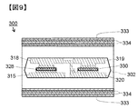
図9は、第5の実施形態を示すパワー半導体モジュール300の分解断面図である。
図9に示すように、絶縁部材333の導体層334に、図3(A)に示すスリット部339が設けられていない。更に、絶縁部材333の導体層334が間に絶縁層を挟んで2層に積層されている。その他の部分は第1の実施形態と同様の構成である。なお、ベース部材307の形状は、第1の実施形態で示した図3(B)の形状でもよく、第2の実施形態で示した図6(A)の形状でもよい。本実施形態によれば、導体層334が2層に積層されているため、更に絶縁性能が向上し、製造工程も簡略化できる。
図9は、第5の実施形態を示すパワー半導体モジュール300の分解断面図である。
図9に示すように、絶縁部材333の導体層334に、図3(A)に示すスリット部339が設けられていない。更に、絶縁部材333の導体層334が間に絶縁層を挟んで2層に積層されている。その他の部分は第1の実施形態と同様の構成である。なお、ベース部材307の形状は、第1の実施形態で示した図3(B)の形状でもよく、第2の実施形態で示した図6(A)の形状でもよい。本実施形態によれば、導体層334が2層に積層されているため、更に絶縁性能が向上し、製造工程も簡略化できる。
(第6の実施形態)
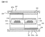
図10は、第6の実施形態を示す分解断面図である。
図10に示すように、絶縁部材333の導体層334は、交流電位の導体板318、320に対向する部分に設け、導体板319、315に対向する部分には設けていない。ベース部材307は、絶縁部材333とベース部材307との接触部分において絶縁部材333側に突出する台状の突出部307aが形成されている。なお、ベース部材307の形状は、第2の実施形態で示した図6(A)の形状でもよい。交流電位の導体板318、320に対向する絶縁部材333とベース部材307との関係は次のとおりである。すなわち、導体層334の中心から絶縁部材333の周縁部までの長さは、導体層334の中心からベース部材307の突出部307aの周縁部までの長さより長く形成されている。その他の部分は第1の実施形態と同様の構成である。本実施形態によれば、導体層334は耐圧が必要な個所に設けられているため、絶縁性能が向上し、製造工程も簡略化できる。
(第7の実施形態)
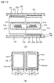
図11(A)(B)は、第7の実施形態の構造を示すパワー半導体モジュール300であり、図11(A)は分解断面図、図11(B)は底部平面図である。
図11(A)に示すように、絶縁部材333が、導体板315、318、319、320にそれぞれ対向する様に分割して配置され、更に、絶縁部材333の導体層334は、交流電位の導体板318、320に対向する部分に設け、導体板319、315に対向する部分には設けていない。ベース部材307には、ベース部材307の中央部に凹部310が設けられている。ベース部材307は、絶縁部材333とベース部材307との接触部分において絶縁部材333側に突出する台状の突出部307aが形成されている。なお、ベース部材307の形状は、第2の実施形態で示した図6(A)の形状でもよい。交流電位の導体板318、320に対向する絶縁部材333とベース部材307との関係を図11(B)に示す。すなわち、導体層334の中心Pから絶縁部材333の周縁部までの長さL10は、導体層334の中心からベース部材307の突出部307aの周縁部までの長さL9より長く形成されている。本実施形態によれば、導体層334は耐圧が必要な個所に設けられているため、絶縁性能が向上し、製造工程も簡略化できる。
以上説明した実施形態によれば、次の作用効果が得られる。
(1)パワー半導体モジュール300は、半導体素子(IGBT328、ダイオード156)と、半導体素子に接続される導体板315、318、319、320と、導体板315、318、319、320と対向し、パワー半導体モジュール300の外装を構成する金属製のベース部材307と、導体板315、318、319、320とベース部材307との間に配置される絶縁部材333と、を備え、絶縁部材333は、第1絶縁層335aと第2絶縁層335bとの間に導体層334を挟んで構成され、第1絶縁層335aと導体板315、318、319、320との間で静電容量回路を形成し、第2絶縁層335bとベース部材307との間で静電容量回路を形成し、ベース部材307は、絶縁部材333とベース部材307との接触部分において絶縁部材333側に突出する台状の突出部307aが形成され、導体層334の中心から導体層334を含む絶縁部材333の周縁部までの長さは、導体層334の中心からベース部材307の突出部307aの周縁部までの長さより長く形成される。これにより、絶縁性を確実に確保できるパワー半導体モジュール300を提供できる。
(1)パワー半導体モジュール300は、半導体素子(IGBT328、ダイオード156)と、半導体素子に接続される導体板315、318、319、320と、導体板315、318、319、320と対向し、パワー半導体モジュール300の外装を構成する金属製のベース部材307と、導体板315、318、319、320とベース部材307との間に配置される絶縁部材333と、を備え、絶縁部材333は、第1絶縁層335aと第2絶縁層335bとの間に導体層334を挟んで構成され、第1絶縁層335aと導体板315、318、319、320との間で静電容量回路を形成し、第2絶縁層335bとベース部材307との間で静電容量回路を形成し、ベース部材307は、絶縁部材333とベース部材307との接触部分において絶縁部材333側に突出する台状の突出部307aが形成され、導体層334の中心から導体層334を含む絶縁部材333の周縁部までの長さは、導体層334の中心からベース部材307の突出部307aの周縁部までの長さより長く形成される。これにより、絶縁性を確実に確保できるパワー半導体モジュール300を提供できる。
本発明は、上記の実施形態に限定されるものではなく、上述した各実施形態を組み合わせた構成としてもよい。また、本発明の特徴を損なわない限り、本発明の技術思想の範囲内で考えられるその他の形態についても、本発明の範囲内に含まれる。
300 パワー半導体モジュール
304 ケース
305 フィン
307 ベース部材
307a 突出部
315、318、319、320 導体板
333 絶縁部材
334 導体層
335a 第1絶縁層
335b 第2絶縁層
304 ケース
305 フィン
307 ベース部材
307a 突出部
315、318、319、320 導体板
333 絶縁部材
334 導体層
335a 第1絶縁層
335b 第2絶縁層
Claims (5)
- 半導体素子と、
前記半導体素子に接続される導体板と、
前記導体板と対向し、半導体装置の外装を構成する金属製のベース部材と、
前記導体板と前記ベース部材との間に配置される絶縁部材と、を備え、
前記絶縁部材は、第1絶縁層と第2絶縁層との間に導体層を挟んで構成され、前記第1絶縁層と前記導体板との間で静電容量回路を形成し、前記第2絶縁層と前記ベース部材との間で静電容量回路を形成し、
前記ベース部材は、前記絶縁部材と前記ベース部材との接触部分において前記絶縁部材側に突出する突出部が形成され、
前記導体層の中心から前記導体層を含む前記絶縁部材の周縁部までの長さは、前記導体層の中心から前記ベース部材の前記突出部の周縁部までの長さより長く形成される半導体装置。 - 請求項1に記載の半導体装置において、
前記導体板は複数の前記半導体素子に対応して複数設けられ、前記導体層は、複数の前記導体板と対向して複数設けられる半導体装置。 - 請求項1または請求項2に記載の半導体装置において、
前記ベース部材の前記突出部の周縁部に凹部を設け、前記導体層の中心から前記導体層を含む前記絶縁部材の周縁部までの長さは、前記導体層の中心から前記ベース部材の前記凹部までの長さより長く形成される半導体装置。 - 請求項2に記載の半導体装置において、
前記絶縁部材は、複数の前記導体板と同数に分割され、分割された複数の前記絶縁部材は複数の前記導体板と夫々対向して配置され、
前記分割された複数の絶縁部材の隣接する間隙位置に対向して前記ベース部材に凹部が形成される半導体装置。 - 請求項2に記載の半導体装置において、
前記絶縁部材は、複数の前記導体板と同数に分割され、分割された複数の前記絶縁部材は複数の前記導体板のうち、交流電位となる前記導体板に対向して配置され、
前記交流電位となる前記導体板に対向して配置された前記絶縁部材の周縁部までの長さが、前記ベース部材の前記突出部の周縁部までの長さより長く形成される半導体装置。
Priority Applications (3)
| Application Number | Priority Date | Filing Date | Title |
|---|---|---|---|
| US16/089,079 US11201143B2 (en) | 2016-03-30 | 2017-01-23 | Semiconductor device with a protruding base member |
| DE112017001071.3T DE112017001071B4 (de) | 2016-03-30 | 2017-01-23 | Halbleitervorrichtung |
| CN201780020105.5A CN109005669B (zh) | 2016-03-30 | 2017-01-23 | 半导体装置 |
Applications Claiming Priority (2)
| Application Number | Priority Date | Filing Date | Title |
|---|---|---|---|
| JP2016067036A JP6719252B2 (ja) | 2016-03-30 | 2016-03-30 | 半導体装置 |
| JP2016-067036 | 2016-03-30 |
Publications (1)
| Publication Number | Publication Date |
|---|---|
| WO2017168992A1 true WO2017168992A1 (ja) | 2017-10-05 |
Family
ID=59964121
Family Applications (1)
| Application Number | Title | Priority Date | Filing Date |
|---|---|---|---|
| PCT/JP2017/002044 Ceased WO2017168992A1 (ja) | 2016-03-30 | 2017-01-23 | 半導体装置 |
Country Status (5)
| Country | Link |
|---|---|
| US (1) | US11201143B2 (ja) |
| JP (1) | JP6719252B2 (ja) |
| CN (1) | CN109005669B (ja) |
| DE (1) | DE112017001071B4 (ja) |
| WO (1) | WO2017168992A1 (ja) |
Cited By (1)
| Publication number | Priority date | Publication date | Assignee | Title |
|---|---|---|---|---|
| WO2020195140A1 (ja) * | 2019-03-28 | 2020-10-01 | 日立オートモティブシステムズ株式会社 | パワー半導体装置 |
Families Citing this family (6)
| Publication number | Priority date | Publication date | Assignee | Title |
|---|---|---|---|---|
| JP7107199B2 (ja) * | 2018-12-07 | 2022-07-27 | 株式会社デンソー | 半導体装置 |
| JP7156155B2 (ja) * | 2019-04-19 | 2022-10-19 | 三菱電機株式会社 | 半導体モジュール |
| JP7356402B2 (ja) * | 2020-05-18 | 2023-10-04 | 日立Astemo株式会社 | パワーモジュール |
| JP7580349B2 (ja) * | 2021-07-01 | 2024-11-11 | 日立Astemo株式会社 | パワー半導体装置 |
| DE112021008369T5 (de) * | 2021-12-15 | 2024-08-01 | Hitachi Astemo, Ltd. | Halbleitervorrichtung und isolierelement |
| CN116130443A (zh) * | 2023-02-16 | 2023-05-16 | 华中科技大学 | 一种用于高温环境的碳化硅功率模块双面散热封装结构 |
Citations (3)
| Publication number | Priority date | Publication date | Assignee | Title |
|---|---|---|---|---|
| JP2013118299A (ja) * | 2011-12-05 | 2013-06-13 | Mitsubishi Materials Corp | パワーモジュール用基板 |
| JP2015126342A (ja) * | 2013-12-26 | 2015-07-06 | ローム株式会社 | パワー回路およびパワーモジュール |
| WO2016038955A1 (ja) * | 2014-09-09 | 2016-03-17 | 日立オートモティブシステムズ株式会社 | パワーモジュール |
Family Cites Families (8)
| Publication number | Priority date | Publication date | Assignee | Title |
|---|---|---|---|---|
| US1006880A (en) | 1910-05-23 | 1911-10-24 | George Roseman | Agricultural machine. |
| JP5492447B2 (ja) * | 2009-04-28 | 2014-05-14 | 日立オートモティブシステムズ株式会社 | パワーモジュール |
| JP5591396B2 (ja) * | 2011-03-04 | 2014-09-17 | 日立オートモティブシステムズ株式会社 | 半導体モジュール、および半導体モジュールの製造方法 |
| JP5825843B2 (ja) | 2011-05-19 | 2015-12-02 | 株式会社日立製作所 | 半導体ユニット及び電力変換装置 |
| JP5520889B2 (ja) | 2011-06-24 | 2014-06-11 | 日立オートモティブシステムズ株式会社 | パワー半導体モジュール及びそれを用いた電力変換装置 |
| JP2013229534A (ja) | 2012-04-27 | 2013-11-07 | Mitsubishi Electric Corp | 半導体装置 |
| JP2013229535A (ja) | 2012-04-27 | 2013-11-07 | Mitsubishi Electric Corp | 半導体装置 |
| KR101420536B1 (ko) * | 2012-12-14 | 2014-07-17 | 삼성전기주식회사 | 전력 모듈 패키지 |
-
2016
- 2016-03-30 JP JP2016067036A patent/JP6719252B2/ja active Active
-
2017
- 2017-01-23 WO PCT/JP2017/002044 patent/WO2017168992A1/ja not_active Ceased
- 2017-01-23 CN CN201780020105.5A patent/CN109005669B/zh active Active
- 2017-01-23 US US16/089,079 patent/US11201143B2/en active Active
- 2017-01-23 DE DE112017001071.3T patent/DE112017001071B4/de active Active
Patent Citations (3)
| Publication number | Priority date | Publication date | Assignee | Title |
|---|---|---|---|---|
| JP2013118299A (ja) * | 2011-12-05 | 2013-06-13 | Mitsubishi Materials Corp | パワーモジュール用基板 |
| JP2015126342A (ja) * | 2013-12-26 | 2015-07-06 | ローム株式会社 | パワー回路およびパワーモジュール |
| WO2016038955A1 (ja) * | 2014-09-09 | 2016-03-17 | 日立オートモティブシステムズ株式会社 | パワーモジュール |
Cited By (5)
| Publication number | Priority date | Publication date | Assignee | Title |
|---|---|---|---|---|
| WO2020195140A1 (ja) * | 2019-03-28 | 2020-10-01 | 日立オートモティブシステムズ株式会社 | パワー半導体装置 |
| JP2020161752A (ja) * | 2019-03-28 | 2020-10-01 | 日立オートモティブシステムズ株式会社 | パワー半導体装置 |
| CN113614917A (zh) * | 2019-03-28 | 2021-11-05 | 日立安斯泰莫株式会社 | 功率半导体装置 |
| JP7240221B2 (ja) | 2019-03-28 | 2023-03-15 | 日立Astemo株式会社 | パワー半導体装置 |
| US11894348B2 (en) | 2019-03-28 | 2024-02-06 | Hitachi Astemo, Ltd. | Power semiconductor device |
Also Published As
| Publication number | Publication date |
|---|---|
| US20200303360A1 (en) | 2020-09-24 |
| DE112017001071T5 (de) | 2018-11-29 |
| DE112017001071B4 (de) | 2026-07-02 |
| CN109005669A (zh) | 2018-12-14 |
| US11201143B2 (en) | 2021-12-14 |
| JP2017183440A (ja) | 2017-10-05 |
| CN109005669B (zh) | 2022-05-10 |
| JP6719252B2 (ja) | 2020-07-08 |
Similar Documents
| Publication | Publication Date | Title |
|---|---|---|
| JP6719252B2 (ja) | 半導体装置 | |
| CN111373647B (zh) | 电力转换装置 | |
| JP6233507B2 (ja) | パワー半導体モジュールおよび複合モジュール | |
| JP6725004B2 (ja) | 半導体装置、インバータユニット及び自動車 | |
| US9973104B2 (en) | Power module | |
| CN107424985B (zh) | 功率模块 | |
| CN110323142B (zh) | 功率模块及其制造方法 | |
| JP6988345B2 (ja) | 半導体装置 | |
| IT201800004209A1 (it) | Dispositivo semiconduttore di potenza con relativo incapsulamento e corrispondente procedimento di fabbricazione | |
| WO2015072105A1 (ja) | パワーモジュール | |
| JP6149932B2 (ja) | 半導体装置 | |
| KR20200011890A (ko) | 중첩 전기 전도성 영역을 갖는 반도체 패키지 및 그 제조 방법 | |
| JP2015162609A (ja) | 半導体装置 | |
| CN103633044A (zh) | 半导体装置 | |
| CN111354710B (zh) | 半导体装置及其制造方法 | |
| CN106972001A (zh) | 半导体模块以及半导体装置 | |
| JP2021180252A (ja) | 半導体装置、バスバー及び電力変換装置 | |
| CN113348554B (zh) | 功率半导体装置 | |
| JP2000058372A (ja) | セラミックコンデンサ実装構造 | |
| CN117501434A (zh) | 功率半导体器件 | |
| KR102016019B1 (ko) | 고열전도성 반도체 패키지 | |
| CN112910287B (zh) | 功率用半导体装置 | |
| WO2022124011A1 (ja) | 積層型コンデンサおよび半導体装置 | |
| JP6584333B2 (ja) | パワーモジュール | |
| JP2007150347A (ja) | セラミックコンデンサ実装構造 |
Legal Events
| Date | Code | Title | Description |
|---|---|---|---|
| WWE | Wipo information: entry into national phase |
Ref document number: 112017001071 Country of ref document: DE |
|
| 121 | Ep: the epo has been informed by wipo that ep was designated in this application |
Ref document number: 17773542 Country of ref document: EP Kind code of ref document: A1 |
|
| 122 | Ep: pct application non-entry in european phase |
Ref document number: 17773542 Country of ref document: EP Kind code of ref document: A1 |
|
| WWG | Wipo information: grant in national office |
Ref document number: 112017001071 Country of ref document: DE |