WO2017164032A1 - 印刷版および印刷方法ならびに印刷版の製造方法 - Google Patents
印刷版および印刷方法ならびに印刷版の製造方法 Download PDFInfo
- Publication number
- WO2017164032A1 WO2017164032A1 PCT/JP2017/010388 JP2017010388W WO2017164032A1 WO 2017164032 A1 WO2017164032 A1 WO 2017164032A1 JP 2017010388 W JP2017010388 W JP 2017010388W WO 2017164032 A1 WO2017164032 A1 WO 2017164032A1
- Authority
- WO
- WIPO (PCT)
- Prior art keywords
- silicone rubber
- printing
- printing plate
- image
- layer containing
- Prior art date
Links
Images


Classifications
-
- B—PERFORMING OPERATIONS; TRANSPORTING
- B41—PRINTING; LINING MACHINES; TYPEWRITERS; STAMPS
- B41N—PRINTING PLATES OR FOILS; MATERIALS FOR SURFACES USED IN PRINTING MACHINES FOR PRINTING, INKING, DAMPING, OR THE LIKE; PREPARING SUCH SURFACES FOR USE AND CONSERVING THEM
- B41N1/00—Printing plates or foils; Materials therefor
- B41N1/12—Printing plates or foils; Materials therefor non-metallic other than stone, e.g. printing plates or foils comprising inorganic materials in an organic matrix
-
- B—PERFORMING OPERATIONS; TRANSPORTING
- B41—PRINTING; LINING MACHINES; TYPEWRITERS; STAMPS
- B41C—PROCESSES FOR THE MANUFACTURE OR REPRODUCTION OF PRINTING SURFACES
- B41C1/00—Forme preparation
- B41C1/003—Forme preparation the relief or intaglio pattern being obtained by imagewise deposition of a liquid, e.g. by an ink jet
-
- B—PERFORMING OPERATIONS; TRANSPORTING
- B41—PRINTING; LINING MACHINES; TYPEWRITERS; STAMPS
- B41C—PROCESSES FOR THE MANUFACTURE OR REPRODUCTION OF PRINTING SURFACES
- B41C1/00—Forme preparation
- B41C1/02—Engraving; Heads therefor
-
- B—PERFORMING OPERATIONS; TRANSPORTING
- B41—PRINTING; LINING MACHINES; TYPEWRITERS; STAMPS
- B41M—PRINTING, DUPLICATING, MARKING, OR COPYING PROCESSES; COLOUR PRINTING
- B41M1/00—Inking and printing with a printer's forme
- B41M1/10—Intaglio printing ; Gravure printing
-
- B—PERFORMING OPERATIONS; TRANSPORTING
- B41—PRINTING; LINING MACHINES; TYPEWRITERS; STAMPS
- B41M—PRINTING, DUPLICATING, MARKING, OR COPYING PROCESSES; COLOUR PRINTING
- B41M1/00—Inking and printing with a printer's forme
- B41M1/26—Printing on other surfaces than ordinary paper
- B41M1/32—Printing on other surfaces than ordinary paper on rubber
-
- G—PHYSICS
- G03—PHOTOGRAPHY; CINEMATOGRAPHY; ANALOGOUS TECHNIQUES USING WAVES OTHER THAN OPTICAL WAVES; ELECTROGRAPHY; HOLOGRAPHY
- G03F—PHOTOMECHANICAL PRODUCTION OF TEXTURED OR PATTERNED SURFACES, e.g. FOR PRINTING, FOR PROCESSING OF SEMICONDUCTOR DEVICES; MATERIALS THEREFOR; ORIGINALS THEREFOR; APPARATUS SPECIALLY ADAPTED THEREFOR
- G03F7/00—Photomechanical, e.g. photolithographic, production of textured or patterned surfaces, e.g. printing surfaces; Materials therefor, e.g. comprising photoresists; Apparatus specially adapted therefor
- G03F7/0005—Production of optical devices or components in so far as characterised by the lithographic processes or materials used therefor
- G03F7/0007—Filters, e.g. additive colour filters; Components for display devices
-
- G—PHYSICS
- G03—PHOTOGRAPHY; CINEMATOGRAPHY; ANALOGOUS TECHNIQUES USING WAVES OTHER THAN OPTICAL WAVES; ELECTROGRAPHY; HOLOGRAPHY
- G03F—PHOTOMECHANICAL PRODUCTION OF TEXTURED OR PATTERNED SURFACES, e.g. FOR PRINTING, FOR PROCESSING OF SEMICONDUCTOR DEVICES; MATERIALS THEREFOR; ORIGINALS THEREFOR; APPARATUS SPECIALLY ADAPTED THEREFOR
- G03F7/00—Photomechanical, e.g. photolithographic, production of textured or patterned surfaces, e.g. printing surfaces; Materials therefor, e.g. comprising photoresists; Apparatus specially adapted therefor
- G03F7/20—Exposure; Apparatus therefor
- G03F7/24—Curved surfaces
-
- H—ELECTRICITY
- H05—ELECTRIC TECHNIQUES NOT OTHERWISE PROVIDED FOR
- H05K—PRINTED CIRCUITS; CASINGS OR CONSTRUCTIONAL DETAILS OF ELECTRIC APPARATUS; MANUFACTURE OF ASSEMBLAGES OF ELECTRICAL COMPONENTS
- H05K3/00—Apparatus or processes for manufacturing printed circuits
- H05K3/10—Apparatus or processes for manufacturing printed circuits in which conductive material is applied to the insulating support in such a manner as to form the desired conductive pattern
- H05K3/12—Apparatus or processes for manufacturing printed circuits in which conductive material is applied to the insulating support in such a manner as to form the desired conductive pattern using thick film techniques, e.g. printing techniques to apply the conductive material or similar techniques for applying conductive paste or ink patterns
-
- B—PERFORMING OPERATIONS; TRANSPORTING
- B41—PRINTING; LINING MACHINES; TYPEWRITERS; STAMPS
- B41M—PRINTING, DUPLICATING, MARKING, OR COPYING PROCESSES; COLOUR PRINTING
- B41M1/00—Inking and printing with a printer's forme
- B41M1/26—Printing on other surfaces than ordinary paper
- B41M1/30—Printing on other surfaces than ordinary paper on organic plastics, horn or similar materials
-
- B—PERFORMING OPERATIONS; TRANSPORTING
- B41—PRINTING; LINING MACHINES; TYPEWRITERS; STAMPS
- B41M—PRINTING, DUPLICATING, MARKING, OR COPYING PROCESSES; COLOUR PRINTING
- B41M1/00—Inking and printing with a printer's forme
- B41M1/26—Printing on other surfaces than ordinary paper
- B41M1/34—Printing on other surfaces than ordinary paper on glass or ceramic surfaces
Definitions
- the present invention relates to a printing plate used for forming a wiring pattern and the like, a printing method using the printing plate, and a manufacturing method of the printing plate, and in particular, a printing plate that can be used for forming a high-definition pattern, and the printing
- the present invention relates to a printing method using a printing plate and a printing plate manufacturing method.
- printing is used not only for writing letters and photographs, but also for forming wiring boards and the like.
- Attempts to produce electronic devices by printing technology using functional materials in inks are expected as new methods for forming passive elements and active electronic elements as well as forming metal wiring.
- a technical field called printing electronics technology is a process at normal pressure and relatively low temperature, and thus it is said that electronic devices can be easily manufactured with low energy, and has attracted attention.
- Patent Document 1 describes a printing intaglio having a concave image portion and a non-image portion formed on a substrate for printing, and the image portion is recessed with respect to the non-image portion. .
- an image portion and a non-image portion are formed on the main surface of the substrate.
- the image portion has a solvent holding layer and a resin layer, and the resin layer has a facing surface facing the main surface of the substrate.
- the solvent holding layer is disposed between the base material and the resin layer.
- the solvent holding layer has a contact surface that is in surface contact with the opposing surface of the resin layer.
- a solvent holding layer and a resin layer are sequentially laminated on the inner surface of the concave portion of the image line portion.
- the non-image area is formed by laminating a metal film on a substrate. Note that the image line portion is a portion where ink is transferred to the substrate during printing. The non-image portion is a portion where ink is not transferred to the substrate during printing.
- Patent Document 2 uses an intaglio transfer method in which a transfer material in a liquid state is filled in a transfer intaglio and is peeled off after the transfer material is cured or solidified to form a desired object made of the transfer material on the transfer target side.
- An intaglio for transfer is described.
- At least a part of the surface layer of the printing plate is made of a substance having a low critical surface tension, or a substance having an action of reducing the critical surface tension is segregated.
- a substance having a low critical surface tension is a block copolymer or a graft copolymer containing a fluororesin or a silicone resin, and can impart photocurability.
- the substance having the action of reducing the critical surface tension is a silicone resin-based additive or a fluororesin-based additive, and the portion where the material of the surface layer of the printing plate is deposited is when the material constituting this portion is in a liquid state.
- a silicone resin-based additive or a fluororesin-based additive is added to a curable material at a certain time, is formed as a surface layer, and is cured after heat treatment.
- Patent Document 3 describes an intaglio plate in which a plate pattern including a concave portion corresponding to an image line portion and a bank portion corresponding to a non-image line portion is provided on the plate base material.
- the bank is elastically deformable, and a part or all of the upper surface of the bank is made of an ink repellent material that repels ink.
- an image is formed on a hard substrate such as a glass substrate by direct printing.
- the non-image portion is formed of a metal film, and the surface is metal.
- the resin layer in the recess is made of silicone rubber, and the surface layer of the recess is silicone rubber.
- the surface of the non-image area is not liquid repellent, and the printing method is also performed by applying ink to the entire plate surface.
- the surface of the non-image area is silicone and not a fluorine-based material. Any of the intaglio plates of Patent Documents 1 to 3 has a problem in that the liquid repellency of the non-image area is not sufficient due to the above-described configuration, and ink overflows from the image area, that is, the recess. Thereby, a high-definition pattern cannot be formed.
- An object of the present invention is to provide a printing plate, a printing method, and a printing plate manufacturing method capable of solving the problems based on the above-described prior art and forming a high-definition pattern.
- the present invention provides a printing plate having an image portion and a non-image portion, wherein the image portion is a recess and includes a layer containing silicone rubber, and the non-image portion is a protrusion. And a layer containing a fluorine compound provided on the surface of the layer containing silicone rubber, and the height difference between the surface of the image part and the surface of the non-image part is more than 0.1 ⁇ m and less than 10 ⁇ m A printing plate characterized by the above is provided.
- the receding contact angle of the non-image part is preferably larger than the advancing contact angle of the image part.
- the printing ink contains a solvent, and the absorption rate of the solvent in the image area is preferably faster than the absorption rate of the solvent in the non-image area.
- the viscosity of the printing ink is preferably 1 mPa ⁇ s or more and 30 mPa ⁇ s or less. Further, it is preferably used for manufacturing an electronic device, and preferably used for forming a wiring pattern or an electrode.
- the present invention is a printing method using a printing plate having an image portion and a non-image portion, wherein the image portion is a recess and is composed of a layer containing silicone rubber, and the non-image portion is a protrusion. And a layer containing a fluorine compound provided on the surface of the layer containing silicone rubber, and the difference in height between the surface of the image area and the surface of the non-image area is more than 0.1 ⁇ m and 10 ⁇ m or less. It is an object of the present invention to provide a printing method comprising: an ink application process for applying a printing ink; and a transfer process for transferring the printing ink applied to an image portion to a substrate. In the ink application process, it is preferable to apply the printing ink to the image portion by an inkjet method. In the ink application process, it is preferable to change the amount of printing ink applied to the image area.
- the present invention has an image part and a non-image part, the image part is a concave part and is composed of a layer containing silicone rubber, and the non-image part is a convex part and is formed on the surface of the layer containing silicone rubber.
- a printing plate manufacturing method comprising a layer containing a fluorine compound and having a height difference between the surface of the image area and the surface of the non-image area of more than 0.1 ⁇ m and not more than 10 ⁇ m, including silicone rubber
- a step of forming a layer containing a compound comprising a layer containing a fluorine compound and having a height difference between the surface of the image area and the surface of the non-image area of more than 0.1 ⁇ m and not more than 10 ⁇ m, including silicone rubber
- the present invention has an image part and a non-image part, the image part is a concave part and is composed of a layer containing silicone rubber, and the non-image part is a convex part and is formed on the surface of the layer containing silicone rubber.
- a printing plate manufacturing method comprising a layer containing a fluorine compound and having a height difference between the surface of the image area and the surface of the non-image area of more than 0.1 ⁇ m and not more than 10 ⁇ m, including silicone rubber And a step of forming a layer containing a fluorine compound on the layer, a layer containing a fluorine compound in a region to be an image portion, and a step of removing a layer containing silicone rubber in a region to be an image portion.
- a method for producing a printing plate is provided.
- the present invention has an image part and a non-image part, the image part is a concave part and is composed of a layer containing silicone rubber, and the non-image part is a convex part and is formed on the surface of the layer containing silicone rubber.
- a printing plate manufacturing method comprising a layer containing a fluorine compound and having a height difference between the surface of the image area and the surface of the non-image area of more than 0.1 ⁇ m and not more than 10 ⁇ m, including silicone rubber And a step of forming a layer containing a fluorosurfactant and a silicone resin on the layer, and a step of removing the layer containing the fluorosurfactant and the silicone resin in a region to be an image portion.
- a method for producing a printing plate is provided.
- the present invention has an image part and a non-image part, the image part is a concave part and is composed of a layer containing silicone rubber, and the non-image part is a convex part and is formed on the surface of the layer containing silicone rubber.
- a method for producing a printing plate comprising a layer containing a fluorine compound and having a height difference between the surface of the image area and the surface of the non-image area of more than 0.1 ⁇ m and 10 ⁇ m or less, wherein A step of forming a layer containing silicone rubber on a support having a convex pattern for forming a layer, a step of peeling a layer containing silicone rubber from the support, and a layer containing a silicone rubber. And a step of forming a layer containing a fluorine compound on the surface of a region to be an image portion.
- a high-definition pattern can be formed.
- the printing method can form a high-definition pattern.
- a printing plate capable of forming a high-definition pattern can be obtained.
- FIG. 3 is a schematic diagram illustrating an image recording unit of the printing apparatus according to the embodiment of the present invention. It is a top view which shows arrangement
- FIG. 1 is a flowchart illustrating a printing method according to an embodiment of the present invention. It is typical sectional drawing which shows the process of the printing method of embodiment of this invention. It is typical sectional drawing which shows the process of the printing method of embodiment of this invention. It is typical sectional drawing which shows the process of the printing method of embodiment of this invention. It is typical sectional drawing which shows the process of the printing method of embodiment of this invention. It is typical sectional drawing which shows the process of the printing method of embodiment of this invention. It is typical sectional drawing which shows the process of the printing method of embodiment of this invention. It is typical sectional drawing which shows the process of the printing method of embodiment of this invention. It is typical sectional drawing which shows the process of the printing method of embodiment of this invention.
- FIG. 6 is a schematic diagram illustrating a printing result of Example 1.
- FIG. 3 is a schematic diagram illustrating a cross-sectional shape of a printing result of Example 1.
- FIG. 4 is a schematic diagram showing a first inking result of Example 1.
- FIG. It is a schematic diagram which shows the 2nd inking result of Example 1.
- FIG. 10 is a schematic diagram illustrating a printing result by first inking according to the first exemplary embodiment.
- FIG. 10 is a schematic diagram illustrating a printing result by second inking according to the first exemplary embodiment.
- 6 is a schematic diagram illustrating a third inking result of Example 1.
- FIG. 6 is a schematic diagram showing an inking result of Comparative Example 1.
- FIG. 6 is a graph showing measurement results of samples 1 to 5 by time-of-flight secondary ion mass spectrometry.
- 6 is a graph showing measurement results of samples 1 to 5 by time-of-flight secondary ion mass spectrometry.
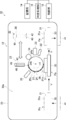
- FIG. 1 is a schematic diagram illustrating an example of a printing apparatus used for printing a printing plate according to an embodiment of the present invention.
- the printing apparatus 10 includes a printing apparatus main body 12, a storage unit 14, a determination processing unit 16, and a control unit 18.
- the printing apparatus main body 12 forms a predetermined pattern on the substrate 31 by a printing method using the printing plate 25.
- the printing apparatus main body 12 will be described in detail later.
- the storage unit 14 stores various information used in the printing apparatus 10.
- the storage unit 14 stores information on a reference shape serving as a reference for the plate surface 25c of the printing plate 25 to which the printing ink is applied to a specific pattern.
- the reference shape information is, for example, image data indicating an ideal state when printing ink is applied to a pattern formation region constituted by the image portion 25a of the printing plate 25.
- the image data indicates an ideal state for each time.
- the ideal dot formed by each printing ink ejection Image data indicating a proper arrangement is referred to as the reference shape information. Further, the image data indicating the ideal state of the plate surface 25c of the printing plate 25 after the transfer is also included in the reference shape information.
- the storage unit 14 stores pattern data of a pattern to be printed.
- the pattern data is appropriately input from the outside.
- the input method of the reference shape information and pattern data to the storage unit 14 is not particularly limited, and various interfaces are provided in the storage unit 14 and input via a storage medium and a wired or wireless network. can do.
- the storage unit 14 corrects the ejection pattern data and ejection timing data of the printing ink ejected from the inkjet head 40 and the ejection pattern data of the printing ink according to the mounting state of the printing plate 25.
- the corrected pattern data is also stored.
- the printing ink ejection pattern data is data indicating ejection patterns when the printing ink is applied to the pattern area of the printing plate 25 using the inkjet head 40.
- the ejection timing data is data indicating when the printing ink is ejected to the pattern area of the printing plate 25 when the printing ink is applied to the pattern area of the printing plate 25 using the inkjet head 40. is there.
- the determination processing unit 16 is used for acquiring attachment information of the printing plate 25 provided in the plate cylinder 24.
- the determination processing unit 16 specifies the positions of the alignment marks A to D using the alignment mark position information obtained by the alignment camera 42 described later. Thereby, attachment information of the printing plate 25 provided on the plate cylinder 24 can be acquired.
- the determination processing unit 16 compares the inclination angle of the printing plate 25 with the allowable range based on the attachment position information of the printing plate 25 and determines whether the printing plate 25 is within the allowable range. Determination information corresponding to the determination result is output to the control unit 18. The inclination angle of the printing plate 25 will be described later.
- the determination processing unit 16 is stored in the storage unit 14 and information on the plate surface 25c of the printing plate 25 obtained by applying the printing ink to the specific pattern obtained by the plate surface observation unit 26 of the printing apparatus main body 12 described later. Compared with the reference shape information serving as a reference of the plate surface 25c of the printing plate 25 to which the printing ink is applied with respect to the specific pattern, it is determined whether the reference pattern is within a predetermined range. is there. Determination information corresponding to the determination result is output to the control unit 18.
- the determination processing unit 16 also identifies a part or the like that is out of the predetermined range. For example, when printing ink is applied to the pattern area, the portion where the printing ink protrudes is specified. Further, in the case where the printing ink is applied to the pattern region by the ink jet method, the determination processing unit 16 can specify a positional deviation of dots formed by the printing ink, a region where dots are missing, and the like. Thereby, as will be described later, the ejection amount of the printing ink is adjusted in accordance with the location specified by the control unit 18.
- the determination processing unit 16 determines the printing ink.
- the ejection pattern data is multiplied by cos ⁇ in accordance with the inclination angle ⁇ to create correction pattern data.
- the correction pattern data is stored in the storage unit 14.
- the correction pattern data is generated by the determination processing unit 16 when the inclination angle ⁇ of the printing plate 25 is compared with the allowable range based on the attachment information of the printing plate 25 and is determined to be out of the allowable range.
- the determination processing unit 16 calculates a rotation amount for rotating the inkjet head 40 based on the attachment position information of the printing plate 25 obtained by the plate surface observation unit 26 and stores the rotation amount in the storage unit 14. Based on the rotation amount, the control unit 18 rotates the inkjet head 40 to discharge printing ink.
- the control unit 18 is connected to the printing apparatus main body 12, the storage unit 14, and the determination processing unit 16, and controls each element of the printing apparatus main body 12, the storage unit 14, and the determination processing unit 16. Further, the control unit 18 controls each unit according to the determination result in the determination processing unit 16. Further, for example, when the correction pattern data of the ejection pattern data is created by the determination processing unit 16, the control unit 18 ejects printing ink from the inkjet head 40 based on the correction pattern data.
- the printing apparatus main body 12 Since the printing apparatus main body 12 has a clean atmosphere for printing, each part is provided in the inside 20 a of the casing 20. A filter (not shown) and air conditioning equipment (not shown) are provided so that the inside 20a of the casing 20 has a predetermined cleanliness.
- the printing apparatus main body 12 includes an image recording unit 22, a plate cylinder 24, a plate surface observation unit 26, a stage 30, a drying unit 32, an ionizer 33, a cleaning unit 34, and a maintenance unit 36.
- An image recording unit 22, a plate surface observation unit 26, a drying unit 32, an ionizer 33 and a cleaning unit 34 are provided so as to surround the surface 24 a of the plate cylinder 24.
- the cleaning unit 34 is provided in contact with the surface 24 a of the plate cylinder 24.
- the substrate 31 is arranged on the stage 30, and the printing plate 25 and the surface 31 a of the substrate 31 come into contact with each other when the plate cylinder 24 rotates in a state where the stage 30 is arranged at the printing position Pp below the plate cylinder 24. Is arranged. As a result, the printing ink applied in a predetermined pattern to the plate surface 25 c of the printing plate 25 is transferred to the surface 31 a of the substrate 31.
- the plate cylinder 24 and the stage 30 constitute a transfer unit 39.
- the printing ink is baked by, for example, heat, light, or the like according to the characteristics of the printing ink. A known material used for baking printing ink using heat and light can be used as appropriate.
- the firing of the printing ink on the substrate 31 may be performed inside or outside the casing 20.
- printing ink is applied to the pattern formation region of the printing plate 25 provided on the plate cylinder 24, but this printing ink application may be completed once, or the printing ink is applied multiple times. May be.
- the plate cylinder 24 is rotated as many times as the printing ink is applied. For example, when printing ink is applied in four times, the plate cylinder 24 is rotated four times. Giving printing ink is called inking. Moreover, it is also called scanning that printing ink is performed once among a plurality of times.
- the image recording unit 22 applies printing ink to a predetermined pattern formation region of the plate surface 25c of the printing plate 25, and the image recording unit 22 applies printing ink to the plate surface 25c with a predetermined pattern.
- the image recording method of the image recording unit 22 is not particularly limited, and for example, an ink jet method is used.
- the plate cylinder 24 is rotatable in one direction, for example, the Y direction, around the rotation shaft 24b.
- the Y direction is the rotational direction.
- the Y direction is also called the feed direction.
- the plate cylinder 24 is rotated while holding the printing plate 25 to transfer the printing ink on the plate surface 25c of the printing plate 25 applied in a predetermined pattern onto the surface 31a of the substrate 31.
- a motor (not shown) for rotating the plate cylinder 24 is provided on the rotating shaft 24b via a gear (not shown) or the like.
- a direct drive motor without a gear can be provided.
- the motor is controlled by the control unit 18.
- the rotary shaft 24b is provided with a rotary encoder (not shown) for detecting the rotation and the rotation amount.
- the rotary encoder is connected to the control unit 18, and the control unit 18 detects the amount of rotation of the plate cylinder 24.
- the substrate 31 to be transferred is not particularly limited, but film substrates such as PEN (polyethylene naphthalate), PET (polyethylene terephthalate) and PC (polycarbonate), glass epoxy substrates, ceramic substrates, and glass substrates are used. be able to. In addition to this, the material of the substrate used for the electronic device can be used as appropriate.
- a rigid substrate such as a glass substrate can be transferred by fixing the substrate 31 on the stage 30 and bringing it into close contact with the plate cylinder 24 as described above.
- a configuration may be adopted in which an impression cylinder is used, and the film is fixed to the impression cylinder and brought into close contact with the plate cylinder 24 for transfer.
- the plate surface observation unit 26 is disposed downstream of the image recording unit 22 in the Y direction of the plate cylinder 24.
- the plate surface observation unit 26 acquires information on the plate surface 25c of the printing plate 25 to which the printing ink is applied.
- the plate surface observation unit 26 also acquires information on the plate surface 25 c of the printing plate 25 after the printing ink is transferred to the substrate 31.
- the configuration of the plate surface observation unit 26 is not particularly limited as long as it can acquire information on the plate surface 25c of the printing plate 25 before and after printing ink transfer. Since the printing plate 25 is often rectangular, it is preferable to use a line sensor and line illumination. In this case, plate surface imaging data is obtained as information on the plate surface 25c.
- the plate surface image data is determined by being compared with the reference shape information by the determination processing unit 16 as described above.
- the line sensor for example, a monochrome CMOS (complementary metal oxide semiconductor) sensor or a CCD (charge coupled device) sensor can be used.
- the line sensor may not be a color sensor in order to observe the shadow of the ejected printing ink droplet.
- a lens and various filters may be provided in front of the line sensor.
- the line-shaped illumination for example, LEDs (light emitting diodes) arranged in a straight line can be used.
- the printing plate observation unit 26 is connected to the control unit 18, and the timing of acquiring information on the printing plate 25 c of the printing plate 25 in the printing plate observation unit 26 is controlled by the control unit 18, and the acquired printing plate 25 c of the printing plate 25. Is stored in the storage unit 14.
- silver gloss develops silver gloss with drying, and a color or a reflectance changes.
- the film thickness can be determined by interference fringes.
- the film thickness can be estimated by measuring the relationship between the film thickness and the interference fringes in advance.
- a polarizing filter may be provided to estimate the film thickness by color. In this case as well, the film thickness can be estimated by measuring the relationship between the film thickness and the color in advance.
- the stage 30 places the substrate 31 and moves in the transport direction V to transport the substrate 31 to a predetermined position.
- the stage 30 is provided with a transport mechanism (not shown).
- the transport mechanism is connected to the control unit 18, and the control unit 18 controls the transport mechanism to move the stage 30 in the transport direction V, thereby changing the position of the stage 30.
- the stage 30 stands by at a start position Ps where the substrate 31 transported from the outside of the casing 20 is placed.
- the stage 30 is moved to the printing position Pp below the plate cylinder 24.
- the stage 30 is moved to the end position Pe with the printed substrate 31 placed thereon, and then the substrate 31 is taken out of the casing 20.
- the stage 30 is moved from the end position Pe to the start position Ps and waits until the substrate 31 is loaded.
- the drying unit 32 is for drying the printing ink on the plate surface 25 c of the printing plate 25.
- the drying method is not particularly limited, and examples thereof include warm air using a fan, blowing cold air, heating using an infrared heater, high-frequency irradiation, and microwave irradiation. If the printing ink on the plate surface 25c of the printing plate 25 can be dried by natural drying, the drying unit 32 is not necessarily provided.
- the degree of drying of the printing ink is not particularly limited, and may be a semi-dried state that is a state before being completely dried.
- the semi-dry state is a state in which a part of the solvent of the printing ink before application is dissipated to the outside.
- a preferable semi-dried state for printing is a state satisfying the following requirements 1 to 3. 1. To the extent that the printing ink does not deform in the horizontal direction due to the stress applied to the printing ink on the plate surface 25c during printing (when the printing ink is transferred from the printing plate 25 to the substrate 31), that is, the pattern shape is not deteriorated by printing. Drying is progressing until it has the elasticity of 2.
- Drying proceeds until the cohesive force of the printing ink increases to such an extent that the printing ink does not cry during printing (the state where the printing ink remains on both the plate surface 25c of the printing plate 25 and the substrate 31 after transfer) does not occur. And 3. Printing ink transfer failure during printing (print ink does not transfer from the plate surface 25c of the printing plate 25 to the substrate 31 after transfer) does not occur, that is, the plate surface 25c of the printing plate 25 is attached to the printing ink. This is a state where the drying does not proceed excessively until the adhesion force becomes larger than the adhesion force between the substrate 31 and the printing ink.
- the ionizer 33 neutralizes static electricity on the plate surface 25 c of the printing plate 25.
- the ionizer 33 removes static electricity from the plate surface 25c of the printing plate 25, and suppresses adhesion of foreign matters such as dust and dirt to the plate surface 25c of the printing plate 25. Further, when the plate surface 25c of the printing plate 25 is charged, the printing ink may be bent. However, the bending of the printing ink can be prevented, and the inkjet ejection accuracy is improved.
- an electrostatic static eliminator can be used. For example, a corona discharge method and an ion generation method can be used.
- the ionizer 33 is provided on the downstream side in the Y direction of the drying unit 32. If the static electricity on the plate surface 25c of the printing plate 25 can be removed before recording by the image recording unit 22, the ionizer 33 is provided.
- the position is not particularly limited.
- the cleaning unit 34 removes the printing ink adhering to the plate cylinder 24 and the printing plate 25. If the cleaning part 34 can remove the printing ink adhering to the plate cylinder 24 and the printing plate 25, the structure will not be specifically limited. For example, the roller is pressed against the plate cylinder 24, the printing ink is transferred to the roller, and the transferred printing ink is wiped off.
- the maintenance unit 36 checks whether the discharge characteristics of the image recording unit 22 exhibit predetermined performance.
- the maintenance unit 36 wipes the nozzles so as to exhibit a predetermined performance.
- the maintenance unit 36 is provided at a position away from the plate cylinder 24.
- the image recording unit 22 is transferred to the maintenance unit 36 via a guide rail (not shown), for example.
- the maintenance unit 36 will be described in detail later.
- FIG. 2 is a schematic diagram illustrating an image recording unit of the printing apparatus according to the embodiment of the present invention.
- An image recording unit 22 using an inkjet method will be described as an example.
- the image recording unit 22 includes an inkjet head 40, an alignment camera 42, a laser displacement meter 44, and a rotation unit 49, which are provided on the carriage 46.
- the carriage 46 can be moved in a direction parallel to the rotation shaft 24 b of the plate cylinder 24 by the linear motor 48, that is, the X direction, and the inkjet head 40 can be moved in the X direction by the carriage 46.
- the position of the carriage 46 can be calculated from a reading value of a linear scale (not shown) provided in the linear motor 48.
- the inkjet head 40 is an ink application unit, and the inkjet head 40 is provided with an ejection control unit 43 for controlling ejection of ink.
- a discharge waveform of the printing ink is adjusted by the discharge control unit 43.
- the discharge controller 43 is connected to the controller 18. In the discharge controller 43, for example, the user can adjust the discharge voltage or the discharge waveform through the user interface. As will be described later, the ink is ejected with the temperature of the printing ink adjusted.
- Alignment camera 42 and laser displacement meter 44 are also connected to control unit 18.
- the carriage 46 is provided with a drive unit (not shown) for moving in the Z direction.
- This drive unit is connected to the control unit 18, and the control unit 18 controls the movement of the carriage 46 in the Z direction. Is done.
- the Z direction is a direction perpendicular to the surface 24 a of the plate cylinder 24.
- the alignment camera 42 is for obtaining positional information of alignment marks for correcting printing ink ejection positions, printing ink ejection timings, and pattern data.
- the configuration of the alignment camera 42 is not particularly limited as long as the alignment marks A to D can be detected.
- the alignment marks A to D are imaged by the alignment camera 42, the imaged data is stored in the storage unit 14, and the positions of the alignment marks A to D are specified by the determination processing unit 16.
- the alignment camera 42 and the determination processing unit 16 function as an attachment position information acquisition unit that acquires attachment information of the printing plate 25 provided in the plate cylinder 24. Based on the position information of the alignment marks A and B, it is possible to obtain information about the printing ink ejection start position in the Y direction, the enlargement / reduction of the printing plate in the X direction, and the inclination angle ⁇ of the printing plate.
- the position information of the alignment marks A and C it is possible to obtain information about the discharge start position of the printing ink in the X direction and the enlargement / reduction information of the printing plate in the Y direction.
- information on the trapezoidal distortion of the printing plate that is, information on the keystone deformation can be obtained from the position information of the alignment marks A to D.
- the printing ink discharge start position is called an inking start position.
- a line La (see FIG. 6) passing through the alignment mark A and the alignment mark C is parallel to the Y direction described above.
- the printing plate 25 is attached to the plate cylinder 24, the printing plate 25 is slightly inclined with respect to the plate cylinder 24.
- Information on the attachment of the printing plate 25 on the plate cylinder 24, for example, information such as the inclination of the printing plate 25 with respect to the Y direction of the plate cylinder 24 can be obtained from the position information of the alignment marks A to D.
- the print ink discharge start position, the position of the inkjet head 40, and the print ink discharge timing are corrected based on the various information obtained above. Any of these corrections may be performed by a known correction method for ejecting ink droplets by inkjet. Further, known correction methods can be used for the enlargement / reduction in the X direction, the enlargement / reduction in the Y direction, the inclination, and the trapezoid correction of the pattern data. Note that it is sufficient that there are at least three alignment marks, and information on enlargement / reduction of the printing plate in the X direction, inclination angle ⁇ of the printing plate, and enlargement / reduction of the printing plate in the Y direction can be obtained.
- the laser displacement meter 44 measures the distance between the inkjet head 40 and the plate surface 25c of the printing plate 25.
- the distance in the Y direction between the alignment mark A and the alignment mark C that is, the AC length, changes due to plate swelling caused by printing ink or changes in plate cylinder diameter + plate thickness due to temperature or the like.
- the printing ink of the inkjet head 40 is ejected at the timing of the rotary encoder, it corresponds to the change of the plate length without receiving the change of the plate cylinder diameter, but the length changes when transferred to the substrate 31. End up.
- the laser displacement meter 44 measures the change in the plate cylinder diameter + plate thickness. Correction is performed based on the measurement result. As a specific example of the correction, the distance fluctuation from the rotating shaft 24b of the plate cylinder 24 to the plate surface 25c of the printing plate 25 is accurately measured, and based on the result, the relative movement of the plate cylinder 24 and the substrate 31 at the time of transfer is measured. For example, changing the speed.
- the temperature of the plate cylinder 24 or the environment is measured, and the table of the relationship between the temperature and the distance between the rotation axis 24b of the plate cylinder 24 and the plate surface 25c of the printing plate 25 prepared in advance is used. Based on the above, it is possible to change the movement relative speed of the plate cylinder 24 and the substrate 31 during transfer. According to the specific example of the correction described above, printing can be performed with high accuracy even if the plate swells or the plate cylinder diameter changes. It is known that when the transfer is performed, if the feed speed on the plate side is different from that on the substrate side, the dimension of the transfer pattern in the feed direction changes.
- the configuration of the laser displacement meter 44 is not particularly limited as long as the distance between the inkjet head 40 and the plate surface 25c of the printing plate 25 can be measured.
- the laser displacement meter 44 can measure the change in the plate cylinder diameter + plate thickness by measuring the distance to the plate surface 25c of the printing plate 25. This can be used for enlargement / reduction in the Y direction. For example, when the diameter of the plate cylinder 24 or the film thickness of the printing plate 25 changes due to a temperature change, the length between the alignment mark A and the alignment mark C changes. This change in length can be used for pattern data correction.
- Alignment accuracy can be increased by using the alignment camera 42 and the laser displacement meter 44 as described above.
- the printing apparatus 10 is used for forming a thin film transistor as will be described later.
- the thin film transistor even a deviation of about 10 ⁇ m results in a characteristic different from the designed characteristic.
- the characteristics vary even if there is a deviation of about 10 ⁇ m. For example, when used for electronic paper, high performance cannot be obtained. Can be suppressed.
- the rotating unit 49 rotates the inkjet head 40 around a line perpendicular to the surface 24 a of the plate cylinder 24.
- the rotating portion 49 can match the orientation of the inkjet head 40 with the inclination of the printing plate 25.
- the method for ejecting the printing ink of the ink jet head 40 is not particularly limited, and the piezoelectric method for ejecting the liquid by utilizing the bending deformation, shear deformation, longitudinal vibration, etc. of the piezoelectric element, and the liquid in the liquid chamber by the heater.
- Various methods can be used such as a thermal method in which a liquid is ejected by using a film boiling phenomenon by heating and an electrostatic method in which an electrostatic force is used.
- the specific configuration of the inkjet head 40 includes a plurality of nozzles 41 that alternately change positions in the Y direction along the X direction over a length corresponding to the entire width of the printing plate 25. Has been placed. By alternately changing the positions in the Y direction along the X direction, the nozzles 41 can be arranged at high density.
- the number of rows in which the nozzles 41 are arranged is not particularly limited, and may be one row, two rows, or more.
- the nozzles 41 may be arranged in a matrix.
- the configuration of the inkjet head 40 is not particularly limited, and for example, the configuration shown in FIG. 4 may be used.
- the configuration is not limited to a configuration in which the plurality of head modules 40a are connected in a row, and a plurality of nozzles 41 of the plurality of head modules 40a are arranged so that the positions in the Y direction are alternately changed along the X direction.
- the head modules 40a may be connected together.
- the discharge control unit 43 can adjust the discharge waveform for each head module 40 a. Further, if the ejection control unit 43 is provided for each head module 40 a, it is possible to adjust the ejection waveform for each ejection control unit 43.
- the application of the printing ink 52 b is not limited to the inkjet head 40, but a blade coating method, a bar coating method, a spray coating method, a dip coating method, a spin coating method, a slit coating method, and a capillary.
- a known method such as a coating method can be appropriately used.
- the ink jet method is preferable when it is necessary to control the ink film thickness.
- durability of the printing plate 25 is improved by inking the printing plate 25 using a non-contact inking method such as an ink jet method and a capillary coating method.
- the printing ink preferably has a viscosity in the range of 1 mPa ⁇ s to 20 mPa ⁇ s.
- the printing ink has a viscosity of 1 mPa ⁇ s to 30 mPa ⁇ s. -It is preferable that it is the range below s. Further, when it is necessary to control the ink film thickness, the ink jet method is suitable.
- FIG. 5 is a schematic diagram illustrating an ink supply mechanism of the printing apparatus according to the embodiment of the present invention.
- the inkjet head 40 is connected to two sub tanks 50 and 58 via pipes 50c and 58c, respectively.
- a deaeration unit 51 is provided in the pipe 50c.
- the deaeration unit 51 degass the printing ink supplied to the inkjet head 40, and a known unit can be used as appropriate.
- the sub tank 50 stores printing ink to be supplied to the ink jet head 40.
- Two water level sensors 50a and a temperature adjustment unit 50b are provided. If the water level sensor 50a can measure the water level of printing ink, the structure will not be specifically limited, A well-known thing can be utilized suitably.
- the temperature adjustment unit 50b adjusts the temperature of the printing ink. Thereby, the temperature of printing ink can be adjusted.
- the temperature of the printing ink is preferably about 15 ° C. to 30 ° C., for example. As long as the temperature adjustment unit 50b can adjust the temperature of printing ink, the structure will not be specifically limited, A well-known thing can be used suitably.
- the sub tank 58 stores printing ink collected from the inkjet head 40.
- Two water level sensors 58a and a temperature adjustment unit 58b are provided. Since the water level sensor 58a has the same configuration as the water level sensor 50a, detailed description thereof is omitted. Since the temperature adjustment unit 58b has the same configuration as the temperature adjustment unit 50b, a detailed description thereof is omitted.
- the circulation unit 60 that moves the printing ink of the sub tank 58 to the sub tank 50.
- the circulation unit 60 includes a pipe 60c that connects the sub tank 50 and the sub tank 58, and a pump 60a and a filter 60b that are provided in the pipe 60c.
- the pump 60a is for adjusting the amount of ink in the sub tank 50 and the sub tank 58.
- the configuration of the pump 60a is not particularly limited as long as the printing ink can be moved between the sub tank 50 and the sub tank 58, and a known pump can be appropriately used.
- the printing ink moving from the sub tank 58 to the sub tank 50 passes through the filter 60b, and at this time, dust and the like are removed.
- a pipe 64c is inserted into each of the sub tank 50 and the sub tank 58, and a pump 64a is provided in the pipe 64c. Further, a pressure sensor 64b is connected to the pipe 64c via a pipe 64d. Although not shown, the pipes 64c and 64d are provided with valves and the like. Thereby, the sub tanks 50 and 58 are filled with nitrogen gas. Further, by changing the filling amount of the nitrogen gas, a pressure difference can be generated between the sub tank 50 and the sub tank 58 and the gas can be easily circulated. The pressure of the sub tank 50 and the sub tank 58 can be measured by the pressure sensor 64b. By using the measurement results of the pressures of the sub tank 50 and the sub tank 58 by the pressure sensor 64b, the meniscus negative pressure and the circulation amount of the inkjet head 40 can be controlled.
- An ink tank 52 is connected to the sub tank 50 via a pipe 62b.
- the pipe 62b is provided with a pump 62a and a filter 62e.
- the ink tank 52 is filled with printing ink 52b.
- the ink tank 52 is provided with a temperature adjustment unit 52a. Since the temperature adjustment unit 52a has the same configuration as the temperature adjustment unit 50b, a detailed description thereof will be omitted.
- a cylinder 62c filled with nitrogen gas is connected to the ink tank 52 via a pipe 62d. As a result, the ink tank 52 is filled with nitrogen gas.
- a cleaning liquid bottle 54 is connected to the sub tank 50 via a pipe 62b.
- the pipe 62b is provided with a pump 62a and a filter 62e.
- the cleaning liquid bottle 54 is filled with a cleaning liquid 54b.
- the cleaning liquid bottle 54 is provided with a temperature adjustment unit 54a. Since the temperature adjustment unit 54a has the same configuration as the temperature adjustment unit 50b, a detailed description thereof is omitted. Further, for example, a cylinder 62c filled with nitrogen gas is connected to the cleaning liquid bottle 54 via a pipe 62d. As a result, the cleaning liquid bottle 54 is filled with nitrogen gas.
- the temperature of the printing ink can be adjusted by the temperature adjustment unit 52a, the temperature of the printing ink is preferably the temperature of the printing ink in the sub tank 50> the temperature of the printing ink in the ink tank 52.
- the sub tank 58 is connected to a waste liquid tank 56 through a pipe 62f.
- a pump 62a is connected to the pipe 62f.
- the printing ink 52b in the sub tank 58 can be moved as waste liquid into the waste liquid tank 56.
- nano metal ink for ink jet can be used.
- ULVAC-made Ag nanometal ink (Ag1teH (model number), L-Ag1TeH (model number)), and Au nanometal ink (cyclododecene solvent) ink jet type can be used.
- various inks can be used as appropriate.
- a rotating roller (not shown) that rotates about the rotation axis is arranged with respect to the inkjet head 40.
- a web (not shown) for cleaning the inkjet head 40 is wound around the circumferential surface of the rotating roller.
- the web is not particularly limited as long as the inkjet head 40 can be cleaned.
- the cleaning liquid is directly applied or sprayed to the inkjet head 40 by the cleaning unit, and the rotating roller is rotated to bring the web into contact with the inkjet head to remove the printing ink 52b.
- the cleaning liquid may be ejected onto the web by the cleaning unit, and the rotary roller may be rotated to bring the web into contact with the inkjet head 40 to remove the printing ink 52b.
- the cleaning liquid for example, a solvent that does not contain solids among ink-soluble solvents or ink components is used.
- Hydrocarbon solvents can be used for ULVAC Ag nanometal ink (Ag1teH (model number), L-Ag1TeH (model number)) and Au nanometal ink (cyclododecene solvent) inkjet type.
- the hydrocarbon solvent for example, toluene, xylene, hexane, tetradecane, and cyclododecene can be used.
- the web includes, for example, wiping cloths such as KB Seiren, Savina (registered trademark), Toray, Toraysee (registered trademark), and Teijin Limited, Nanofront (registered trademark), Microstar (registered trademark), etc. Can be used.
- wiping cloths such as KB Seiren, Savina (registered trademark), Toray, Toraysee (registered trademark), and Teijin Limited, Nanofront (registered trademark), Microstar (registered trademark), etc. Can be used.
- the cleaning of the inkjet head 40 is not limited to the above.
- it can also be set as the structure which has a rubber blade (not shown). Since the inkjet head 40 can be moved in the X direction by the carriage 46, the rubber blade is fixed and the printing ink is wiped off in the longitudinal direction of the inkjet head 40 using this.
- the inkjet head 40 may be fixed and the rubber blade may be scanned and wiped. At this time, wiping the printing ink in a short direction perpendicular to the longitudinal direction of the inkjet head 40 has an advantage that the moving distance of the rubber blade can be shortened. There are few merits.
- wiping the printing ink in a direction parallel to the longitudinal direction of the inkjet head 40 has an advantage that the X axis of the inkjet head 40 can be shared. Therefore, it is preferable to design in an optimum form considering the device configuration or cost.
- the cleaning ink may be applied to the rubber blade or the inkjet head 40 to wipe off the printing ink.
- the pressure in the sub tanks 50 and 58 can be set separately from the pressure at the time of printing. It is preferable to set an optimum pressure according to the conditions of the printing ink, the inkjet head 40 or the wipe.
- the web When using a web (not shown), the web is moved and wiped while moving the inkjet head 40 in the X direction, for example. This constantly refreshes the web surface.
- the same web as that described above can be used as the web.
- at least one of cleaning the web with a cleaning liquid in advance and wiping the printing ink, and applying the cleaning liquid to the inkjet head 40 and wiping the printing ink may be performed.
- the pressure in the sub tanks 50 and 58 can be set separately from the pressure at the time of printing. It is preferable to set an optimum pressure according to the conditions of the printing ink, the inkjet head 40 or the wipe.
- the maintenance unit 36 can also perform operations such as purge, spit and drip on the inkjet head 40.
- purging means that the inkjet head 40 is disposed on an ink receiver (not shown), and in this state, the pressure of the sub tank 50 is set to a positive pressure and printing ink is pushed out from the nozzles 41.
- the ink receiver can be shared with the cap and the wiper.
- Spit means discharge operation. Thereby, nozzle clogging and discharge bending can be improved.
- the spit is performed at the same place as the purge, but a spit station may be provided. In this case, it is preferable to perform suction from below so that the ejected printing ink does not fly.
- the drive voltage is made higher than the ejection waveform for the inkjet head 40 during printing, or a dedicated waveform is used.
- the dedicated waveform is set so that the amount of ink droplets is larger than the ejection waveform during printing, and the ejection speed of printing ink is increased.
- the drip is not a recovery operation in which the printing ink is strongly pushed out as in the above-described purge, but an operation in which the printing ink is recovered by dripping slowly. This can improve nozzle clogging and printing ink ejection bending.
- the drip is also performed at the same place as the purge or spit, but the drip is performed by setting the pressure in the sub tank 50 to the positive pressure side than the pressure during printing. However, it is preferable that the pressure in the subtank 50 is more positive than atmospheric pressure and lower than the purge pressure.
- the maintenance unit 36 may have a cap mechanism (not shown) for preventing the nozzle 41 from drying.
- the cap mechanism after the nozzle 41 is capped, the periphery of the nozzle 41 is filled with nitrogen gas. Further, the nozzle 41 can be further prevented from drying by immersing the cleaning liquid in a web or the like and disposing it in the cap.
- the maintenance unit 36 may have a function of observing the printing ink 52b ejected from the inkjet head 40.
- a nozzle observation unit (not shown) for observing the ink droplets 45 ejected from the ink jet head 40 and a nozzle observation for observing the nozzle 41 (see FIG. 3) of the ink jet head 40 from the surface side on which the nozzle 41 is formed. Part (not shown).
- Both the discharge observation unit and the nozzle observation unit are connected to the control unit 18, and their operations are controlled by the control unit 18, and the obtained imaging data is stored in the storage unit 14 by the control unit 18.
- the control unit 18 compares the ejection state of the printing ink with the inkjet head 40 with, for example, the design value of the ejection characteristics of the inkjet head 40, and the comparison result is stored in the storage unit 14.
- FIG. 6 is a schematic plan view showing a printing plate according to an embodiment of the present invention
- FIG. 7 is a schematic sectional view showing an example of a printing plate according to an embodiment of the present invention
- FIG. 8 is an embodiment of the present invention. It is a typical sectional view showing other examples of the printing plate.
- FIG. 9 is a schematic plan view showing an example of the printing pattern of the printing plate according to the embodiment of the present invention.
- the printing plate 25 is provided with alignment marks A to D at four corners, respectively, and an ejection confirmation area T, printing areas G 11 and G 12 , a spit area G, and a printing area G. 21 , G 22 , a spit area G, and printing areas G 31 and G 32 are formed.
- the ejection confirmation area T is an area where printing ink is ejected in a test pattern by the inkjet head 40. After the evaluation, the printing ink in the discharge confirmation area T is removed by the cleaning unit 34 or transferred to the substrate 31 and removed.
- the spit area G is an area that is used for ejection confirmation by ejecting printing ink by the inkjet head 40 in a normal ejection operation.
- the printing plate 25 shown in FIG. 7 has an image portion 25a and a non-image portion 25b other than the image portion 25a.
- the image portion 25a is the concave portion 27, which is a pattern formation region.
- the image portion 25a that is, the concave portion 27 is composed of a layer containing silicone rubber as will be described later.
- the non-image portion 25b is a convex portion and is a non-pattern forming region.
- the non-image portion 25b, that is, the convex portion is formed of a layer containing a fluorine compound as will be described later.
- the pattern formation region is a region for forming, for example, a gate electrode and a wiring. In the printing plate 25, the printing ink is transferred from the image portion 25a to the substrate 31, and the printing ink is not transferred from the non-image portion 25b to the substrate 31.
- a silicone rubber layer 92 is provided on a support material 90.
- a silicone rubber layer 93 is provided as a partition wall of the recess 27 except for the image portion 25a.
- the recess 27 includes a silicone rubber layer 92 and a silicone rubber layer 93 that are layers containing silicone rubber.
- the bottom surface is the surface 92a of the silicone rubber layer 92
- the side surface 27b of the concave portion 27 is composed of a silicone rubber layer 93 that is a layer containing silicone rubber.
- the convex part of the printing plate 25 is comprised by the silicone rubber layer 93, and the fluorine compound layer 94 which is a layer containing a fluorine compound is provided in the surface 93a of the silicone rubber layer 93.
- FIG. The surface 94a of the fluorine compound layer 94 becomes the surface of the non-image portion 25b.
- the fluorine compound layer 94 repels printing ink and exhibits liquid repellency with respect to printing ink.
- the printing plate 25 is generally called an intaglio.
- the height difference ⁇ between the surface of the image portion 25a and the surface of the non-image portion 25b is more than 0.1 ⁇ m and not more than 10 ⁇ m.
- the height difference ⁇ of the printing plate 25 is the distance from the surface 92a of the silicone rubber layer 92 to the surface 94a of the fluorine compound layer 94.
- a cross-sectional image of the printing plate 25 can be obtained using a scanning electron microscope, and the height difference ⁇ can be obtained from the cross-sectional image.
- the fluorine compound layer 94 may have a thickness of 1 nm or more and 100 nm or less, and is preferably about 10 nm, for example. If the fluorine compound layer 94 has a thickness of 1 nm or more, absorption of the solvent can be prevented. By absorbing the solvent of the printing ink in the silicone rubber layers 92 and 93, the printing ink is prevented from being repelled in the silicone rubber layers 92 and 93, and the printing ink can be applied to the silicone rubber layers 92 and 93. Further, by reducing the absorption of the solvent of the printing ink into the fluorine compound, pinning of the printing ink on the fluorine compound layer 94 can be prevented so that the printing ink does not remain on the fluorine compound.
- the image portion 25a is lyophilic with respect to the printing ink and is a lyophilic portion.
- the non-image portion 25b is liquid repellent with respect to printing ink and is an ink repellent portion.
- the silicone rubber layer 92 and the silicone rubber layer 93 are provided in the printing plate 25 shown in FIG. 7, the silicone rubber layer 92 and the silicone rubber layer 93 are provided.
- the present invention is not limited to this.
- the silicone rubber layer 92 may be provided with a recess 27.
- the recessed part 27 is comprised only by the silicone rubber layer 92 including the side surface 27b.
- a fluorine compound layer 94 is provided on the outermost surface 92 c of the convex portion 92 b of the silicone rubber layer 92.
- the image portion 25a and the non-image portion 25b are formed in a specific pattern.
- the pattern of the image portion 25a is, for example, a pattern of a gate electrode and wiring, and the gate electrode and wiring are formed.
- the printing plate 25 can be used, for example, for forming various electrodes such as a gate electrode, a source electrode, and a drain electrode of a thin film transistor used for electronic paper or the like.
- the printing plate 25 can also be used to form wiring patterns for electronic circuits and printed wiring boards.
- FIG. 10 is a schematic view showing an example of a thin film transistor formed using the printing plate of the embodiment of the present invention. 10 includes a gate electrode 82, a gate insulating layer (not shown), a source electrode 86a, a drain electrode 86b, a semiconductor layer (not shown), and a protective layer. (Not shown).
- a gate insulating layer (not shown) is formed so as to cover the gate electrode 82.
- a source electrode 86 a and a drain electrode 86 b are formed on the gate insulating layer with a gap set in advance as a channel region 84.
- a semiconductor layer (not shown) that functions as an active layer is formed on the channel region 84.
- a protective layer (not shown) is formed to cover the semiconductor layer, the source electrode 86a, and the drain electrode 86b.
- the channel length of the channel region 84 is on the order of several ⁇ m to several tens of ⁇ m.
- the drain current of the thin film transistor is affected by the channel length, and the variation in the channel length leads to the variation in the characteristics of the thin film transistor.
- the printing plate 25 can be used for forming various pattern films such as an electrode film, a wiring film, and an insulating film.
- electronic devices such as an electroluminescent transistor, an organic electroluminescent element, and a solar cell can be manufactured by sequentially laminating and forming such various films.
- the printing plate 25 can also be used for manufacturing electronic devices.
- the support material 90 of the printing plate 25 supports the silicone rubber layer 92 and is made of, for example, resin, metal, glass, or the like. Further, the support member 90 is not limited to being composed of only one type of material, and a plurality of materials may be combined. In this case, for example, the support material 90 may be a composite material of an aluminum plate and a polyethylene terephthalate material.
- the printing plate 25 may be configured without the support material 90. When the printing plate 25 is wound around the plate cylinder 24, the support member 90 needs to be flexible. Therefore, for example, when the support material 90 is a polyethylene terephthalate (PET) material, the thickness is desirably about 50 to 200 ⁇ m. When the support member 90 is an aluminum plate, the thickness of the aluminum plate is preferably 0.1 to 1 mm, and preferably 0.15 to 0.4 mm.
- PET polyethylene terephthalate
- the silicone rubber layer 92 of the printing plate 25 constitutes the image portion 25a.
- the silicone rubber refers to a rubbery substance having a network structure having an organic siloxane as a main chain.
- Silicone resins include those that do not exhibit rubber elasticity, for example, organosiloxane polymers.
- the silicone resin also includes silicone rubber as described above.
- the silicone rubber layer 92 of the printing plate 25 is made of, for example, PDMS (polydimethylsiloxane).
- PDMS polydimethylsiloxane
- polydimethylsiloxane is also simply referred to as PDMS.
- the silicone rubber layer 92 is made of, for example, ultraviolet curable PDMS (polydimethylsiloxane) or thermosetting PDMS (polydimethylsiloxane).
- ultraviolet curable PDMS polydimethylsiloxane
- thermosetting PDMS polydimethylsiloxane
- the silicone rubber layer 92 is, for example, an ultraviolet curable liquid silicone rubber (product name: X-34-4184-A / B) manufactured by Shin-Etsu Silicone.
- the thickness of the silicone rubber layer 92 is thicker than the silicone rubber layer 93, for example, about 500 ⁇ m.
- the silicone rubber layer 93 constitutes the side surface 27b of the recess 27, and the height difference ⁇ can be adjusted by the thickness of the silicone rubber layer 93 as described above.
- the thickness of the silicone rubber layer 93 is, for example, about several ⁇ m to 10 ⁇ m, and is appropriately set according to the above-described height difference ⁇ of the printing plate 25.
- the silicone rubber layer 93 is provided on the surface 92 a of the silicone rubber layer 92, and may be composed of PDMS (polydimethylsiloxane) in the same manner as the silicone rubber layer 92.
- the silicone rubber layer 93 is separate from the silicone rubber layer 92 and constitutes the side surface 27b of the recess 27 as described above.
- the silicone rubber layer 93 is capable of pattern formation.
- the silicone rubber layer 93 is made of, for example, ultraviolet curable PDMS (polydimethylsiloxane) or thermosetting PDMS (polydimethylsiloxane).
- ultraviolet curable PDMS polydimethylsiloxane
- thermosetting PDMS polydimethylsiloxane
- the ultraviolet curable PDMS either a type in which a region irradiated with ultraviolet light is cured or a type in which a region irradiated with ultraviolet light is softened can be used depending on the manufacturing method.
- UV curable PDMS polydimethylsiloxane
- UV curable liquid silicone rubber product name: X-34-4184-A / B
- Shin-Etsu Silicone Co., Ltd. a two-component mixed room temperature curing type KE106 (product name), X-32-3279 (prototype number), and X-32-3094-2 (prototype number) manufactured by Shin-Etsu Silicone may be used. it can.
- the thickness of the silicone rubber layer 92 is preferably 10 ⁇ m or more and 1 mm or less. If the thickness of the silicone rubber layer 92 is too thin, less than 10 ⁇ m, the absorption rate of the printing ink solvent is undesirably lowered. On the other hand, if the thickness of the silicone rubber layer 92 exceeds 1 mm, it is not preferable because the deformation of the silicone rubber layer 92 increases due to stress applied during printing, resulting in deterioration of dimensional reproducibility and alignment accuracy. Note that the absorption rate v s of the solvent of the printing ink described later, for greatly varies depending on the solvent of the printing ink used, also changes the lower limit value of the thickness of the preferred silicone rubber layer 92 accordingly.
- the fluorine compound layer 94 of the printing plate 25 constitutes the non-image part 25b.
- the fluorine compound layer 94 preferably exhibits high adhesion to the surface 93a of the silicone rubber layer 93 in addition to exhibiting liquid repellency with respect to the printing ink described later.
- the fluorine compound layer 94 is preferably a polymer mainly composed of a fluoroalkyl group.
- the fluorine compound layer 94 is made of, for example, Durasurf (registered trademark) (DS-5210TH (product name)) manufactured by Harves Co., Ltd. or OPTOOL (registered trademark) DSX (product name) manufactured by Daikin Industries, Ltd. Can do.
- the fluorine compound layer 94 is preferably 1 nm to 100 nm.
- the liquid repellency with respect to the printing ink and the lyophilicity with respect to the printing ink can be evaluated as follows. Droplets are deposited on a region where liquid repellency is expected and a region where lyophilicity is expected, and evaluation is performed based on the behavior of the droplets. A region where the droplet amount is reduced with respect to the droplet amount upon landing is an ink repellent portion having liquid repellency, and a region where the droplet amount is increased is a lyophilic ink portion having lyophilic property. In the plate making process, liquid repellency and lyophilicity are imparted.
- the evaluation of the liquid repellency and the lyophilic property is performed by making droplets land on the boundary between the liquid repellant ink repellant portion and the lyophilic parent ink portion and evaluating the behavior of the liquid droplets.
- a region where the droplet amount has decreased with respect to the droplet amount upon landing is lyophobic, and a region where the droplet amount has increased is lyophilic.
- the advancing contact angle of the printing ink in the image portion 25a is ⁇ A, s and the receding contact angle of the printing ink in the non-image portion 25b is ⁇ R, f , the advancing contact angle of the image portion 25a with respect to the printing ink.
- the receding contact angle ⁇ R , f of the non-image portion 25b is larger than ⁇ A , s .
- the difference between the receding contact angle ⁇ R, f and the advancing contact angle ⁇ A, s is 10 ° or more.
- the printing ink present at the boundary is a liquid-repellent ink repellent portion (non-image) Part 25b) to the lyophilic lyophilic ink part (image part 25a).
- the printing ink straddling the boundary between the image portion 25a and the non-image portion 25b is subjected to a force F having a magnitude indicated by the following formula in the direction from the non-image portion 25b to the image portion 25a.
- ⁇ is the surface tension of the printing ink
- r is the contact surface radius of the droplet.
- the receding contact angle ⁇ R, f and the advancing contact angle ⁇ A, s are less than 180 ° (all droplets satisfy this condition), F is positive if ⁇ R, f > ⁇ A, s.
- the liquid droplet moves to the image portion 25a side.
- the difference between the receding contact angle ⁇ R, f and the advancing contact angle ⁇ A, s is 10 ° or more.
- the advancing contact angle and the receding contact angle can be measured by any of the “tilting method (also referred to as sliding method)”, “Wilhelmy method”, or “expansion / contraction method”. In the present invention, the measurement was performed by the “tilting method (also referred to as sliding method)”.
- the printing ink contains a solvent, and the absorption speed of the solvent in the image portion 25a is higher than the absorption speed of the solvent in the non-image portion 25b with respect to the same solvent. That is, the absorption rate of the solvent of the image portion 25a and v s, when the rate of absorption of the non-image area 25b solvents and v f, it is preferable that v f ⁇ v s. Accordingly, the spread of the printing ink on the image portion 25a is suppressed during printing ink transfer, and a high-definition pattern can be formed.
- absorption rate v s of the solvent of the printing ink in the image area 25a is 0.1 [mu] m / s or more, more preferably 1.0 .mu.m / s or more.
- the solvent absorption speed v f of the printing ink in the non-image area 25b is preferably less than 0.1 ⁇ m / s, more preferably less than 0.01 ⁇ m / s.
- the advancing contact angle and the receding contact angle described above can be adjusted by adding a surfactant to the printing ink solvent.
- absorption rate v s of the solvent of the printing ink It explained absorption rate v s of the solvent of the printing ink.
- Absorption rate v s of the solvent of the printing ink first, the image portion of the printing ink by the ink jet method, the non-image portion is dripping, imaged by the camera the shape of the printing ink dripping from the side. Next, by calculating the amount of ink remaining on the image part and non-image part by performing image processing of the ink shape imaged at every elapsed time from the landing, the ink amount is differentiated by time. Get the solvent absorption rate and evaporation rate of the printing ink.
- the desirable amount of the fluorine compound to be applied to the non-image portion 25b includes the thickness of the fluorine compound layer 94 of the printing plate 25, the receding contact angle ⁇ R, f and the advancing contact angle ⁇ A, s described above, and the above-mentioned. it is those comprehensive judgment combined absorption rate v s of the solvent of the printing ink.
- the desirable amount of the fluorine compound to be applied to the non-image area 25b is derived from the amount of the fluorine compound determined by time-of-flight secondary ion mass spectrometry (TOF-SIMS) and the PDMS-derived amount.
- F / Si ratio [C 3 OF 7 ] / ([Si 3 O 7 H] + [Si 3 C 5 H 15 O 4 ])
- 11 to 15 are schematic cross-sectional views showing the manufacturing method of the first example of the printing plate 25 in the order of steps. 11 to 15, the same components as those of the printing plate 25 shown in FIG. 8 are denoted by the same reference numerals, and detailed description thereof is omitted.
- a support material 90 provided with a silicone rubber layer 92 as a first layer containing silicone rubber is prepared.
- the silicone rubber layer 92 is composed of the above-described ultraviolet curable PDMS or thermosetting PDMS.
- photosensitive PDMS is applied on the silicone rubber layer 92 to form the silicone rubber layer 100.
- the photosensitive PDMS for example, the above-described ultraviolet curable PDMS is used.
- the region irradiated with the ultraviolet light Lv is cured.
- the ultraviolet light Lv is obtained by a general ultraviolet exposure apparatus used in a semiconductor manufacturing apparatus.
- the ultraviolet light Lv it is preferable to use light having a wavelength of 300 nm or less in order to dissociate chemical bonds such as fluorine compounds.
- a mask 110 is disposed on the silicone rubber layer 100.
- the mask 110 transmits the ultraviolet light Lv except for the chromium layer 110a, the region 110b that transmits the ultraviolet light Lv is formed in a pattern of the non-image portion 25b, and the chromium layer 110a is the pattern of the image portion 25a. It is formed in a shape.
- the ultraviolet light Lv is irradiated from above the mask 110 toward the silicone rubber layer 100.
- the irradiated region 100a of the silicone rubber layer 100 is cured, and the unirradiated region 100b that is not irradiated is not cured.
- the unirradiated region 100b is a region that becomes the image portion 25a.
- the mask 110 is removed from the silicone rubber layer 100.
- post-baking is performed on the silicone rubber layer 100 after being irradiated with the ultraviolet light Lv, for example, by holding it in a room temperature atmosphere for a predetermined time.
- the post-baking promotes the curing of the silicone rubber layer 100.
- the silicone rubber layer 100 is developed using toluene, and the unirradiated region 100b is dissolved and removed. As shown in FIG.
- a part of the surface 92a of the silicone rubber layer 92 Is exposed, and a silicone rubber layer 93 is formed as a second layer containing silicone rubber in a region to be the non-image portion 25b on the surface 92a of the silicone rubber layer 92.
- thermosetting PDMS is used as a mold as in the formation of the silicone rubber layer 92 and the convex portion 92b of the silicone rubber layer 92 shown in FIG.
- a casting method may be used.
- the mold material to be used include glass, metal, Si, and resist.
- the resist is a resist layer patterned on a glass substrate or the like.
- the thickness of the silicone rubber layer 93 that is, the depth of the concave portion 27 can be made multi-step within the plane of the printing plate 25. If this method is used, the range of the applied amount of printing ink described later can be further expanded.
- the above-described mask 110 is arranged on the silicone rubber layer 93 so that the region 110 b that transmits the ultraviolet light Lv and the surface 93 a of the silicone rubber layer 93 are aligned.
- the ultraviolet light Lv is irradiated toward the surface 93a. Hydroxyl groups are formed on the surface 93a of the silicone rubber layer 93 irradiated with the ultraviolet light Lv, and the surface 93a is activated.
- the mask 110 is removed from the silicone rubber layer 93.
- the silicone rubber layer 93 together with the support material 90 is immersed in a silane coupling agent (not shown), and the activated surface 93a of the silicone rubber layer 93 is subjected to a silane coupling treatment. Thereafter, the unreacted silane coupling agent is removed by rotating it with a spin coater. Let it settle.
- a silane coupling agent for example, a primer agent dedicated to durasurf (DS-PC-3B (model number)) is used.
- a fluorine compound (not shown) is applied to the surface 93a of the silicone rubber layer 93, and a fixing process is performed at a predetermined temperature and time. Thereafter, the unfixed portion of the fluorine compound is removed by washing, for example, by spin coating with a fluorine-based solvent (Durasurf (DS-TH (product name)) manufactured by Harves Inc.). Thereby, the intaglio printing plate 25 shown in FIG. 7 can be obtained.
- a fluorine-based solvent for example, Durasurf (DS-5210TH (product name)) manufactured by Harves Co., Ltd. or OPTOOL (registered trademark) DSX (product name) manufactured by Daikin Industries, Ltd. is used.
- silane coupling treatment it is desirable to start treatment immediately after exposure, specifically, to immerse in a silane coupling agent within 30 seconds after exposure. This is because the surface radicals formed on the surface of the irradiated area by the exposure treatment are deactivated in a short time and the uncrosslinked component inside the silicone rubber layer 92 is bleed, so that the surface of the irradiated area gradually becomes a hydrophobic surface. It is because it will return to.
- a mask exposure method using the mask 110 is used, but the present invention is not limited to this.
- Plasma treatment using a mask having an opening, laser or light collection A direct drawing method in which the light beam is directly scanned can also be used.
- the activated surface 93a when the activated surface 93a is subjected to a silane coupling treatment, a liquid phase method in which the surface 93a is immersed in a silane coupling agent is used.
- the activated surface 93a may be subjected to a silane coupling treatment using a gas of a silane coupling agent.
- chemical or physical treatment is performed to improve the degree of activation of the surface 92a of the silicone rubber layer 92 and the side surface 93b of the silicone rubber layer 93. Can do.
- the fluorine compound is applied after the silane coupling treatment, but the present invention is not limited to this.
- a fluorine-based silane coupling agent is bonded to the above-described hydroxyl group by a vapor phase method or a liquid phase method.
- the fluorine compound layer 94 (see FIG. 7) may be formed.
- FIG. 16 and FIG. 17 are schematic cross-sectional views showing the manufacturing method of the second example of the printing plate 25 in the order of steps.
- the same components as those of the printing plate 25 shown in FIG.
- the ultraviolet light is irradiated on the silicone rubber layer 92 including the surface 93a of the silicone rubber layer 93.
- Lv is irradiated to form hydroxyl groups on the entire surface 93a of the silicone rubber layer 93, thereby bringing the surface 93a of the silicone rubber layer 93 into an activated state.
- the surface 92a of the silicone rubber layer 92 is also activated, and when the side surface 93b of the silicone rubber layer 93 is irradiated with the ultraviolet light L, the side surface 93b is also activated.
- the method is not limited to the method using the ultraviolet curable PDMS described above, and the thermosetting PDMS is used as a mold as in the formation of the silicone rubber layer 92 and the convex portion 92b of the silicone rubber layer 92 shown in FIG.
- a casting method may be used.
- the mold material used is as described above.
- the base body 112 containing a silane coupling agent is pressed and brought into contact only with the surface 93a of the silicone rubber layer 93, and the surface 93a is subjected to silane coupling treatment. Thereafter, a fluorine compound layer 94 (see FIG. 7) is formed on the surface 93a that has been subjected to the silane coupling treatment.
- the method for forming the fluorine compound layer 94 is as described above.
- the substrate 112 containing the silane coupling agent can be formed by immersing the base material of the substrate 112 in a solution in which the silane coupling agent is dissolved for a certain period of time.
- the material used for the base material of the substrate 112 may be any material that absorbs the silane coupling agent and its solvent, and is composed of, for example, PDMS. Moreover, what is necessary is just to determine suitably the time which immerses a base material in the solution in which the silane coupling agent melt
- the method is not limited to the above-described method.
- the base 112 containing a fluorine-based silane coupling agent is pressed and brought into contact with only the surface 93a of the silicone rubber layer 93, and the fluorine compound layer is brought into contact with the surface 93a.
- the base material of the base 112 is made of, for example, PDMS, SHIN-ETSU SIFEL (registered trademark) manufactured by Shin-Etsu Chemical Co., Ltd., Daiel (registered trademark) manufactured by Daikin Industries, Ltd., or the like.
- the silane coupling treatment method is as described above.
- the substrate 112 containing a fluorine compound is pressed and brought into contact only with the surface 93a that has been subjected to the silane coupling treatment to form a fluorine compound layer 94 (see FIG. 8).
- the intaglio printing plate 25 shown in FIG. 8 can be obtained.
- the configuration of the base material of the base body 112 is as described above.
- 18 to 21 are schematic cross-sectional views showing the manufacturing method of the third example of the printing plate 25 in the order of steps.
- 18 to 21 the same components as those of the printing plate 25 shown in FIG. 8 are denoted by the same reference numerals, and detailed description thereof is omitted.
- a resist is filled into the recesses 93 c of the silicone rubber layer 93 to form a resist layer 114.
- the resist is not particularly limited as long as the resist layer 114 can be formed on the silicone rubber layer 92, and a known resist can be appropriately used.
- thermosetting PDMS is cast into a mold and molded as in the formation of the silicone rubber layer 92 and the convex portion 92b of the silicone rubber layer 92 shown in FIG. 8 may be used.
- the mold material used is as described above.
- the resist layer 114 preferably has a low transmittance of the ultraviolet light Lv, that is, a high absorption rate of the ultraviolet light Lv. Thereby, irradiation of the ultraviolet light Lv to the part provided with the resist layer 114 can be suppressed.
- the surface 93 a of the silicone rubber layer 93 is irradiated with ultraviolet light Lv including the resist layer 114. Thereby, a hydroxyl group is formed on the surface 93a of the silicone rubber layer 93, and the surface 93a is activated.
- the activated surface 93a is subjected to a silane coupling treatment, and then a fluorine compound layer 94 is formed on the surface 93a subjected to the silane coupling treatment, as shown in FIG. . Since the silane coupling process is as described above, a detailed description is omitted.
- the method for forming the fluorine compound layer 94 is the same as the method for forming the fluorine compound layer 94 described above.
- the resist layer 114 is removed.
- a known removal method of the resist layer 114 used in a photolithography method can be used as appropriate.
- the resist layer 114 is removed by dissolving the resist layer 114 using a solvent. Thereby, the printing plate 25 shown in FIG. 8 can be obtained.
- 22 to 25 are schematic cross-sectional views showing the manufacturing method of the fourth example of the printing plate 25 in the order of steps. 22 to 25, the same components as those of the printing plate 25 shown in FIG. 8 are denoted by the same reference numerals, and detailed description thereof is omitted.
- the resist is used to fill the recesses 93c of the silicone rubber layer 93 as shown in FIG.
- a resist layer 115 is formed to cover the surface 93a of the 93.
- the resist is not particularly limited as long as the resist layer 115 can be formed on the silicone rubber layer 92, and a known resist can be appropriately used.
- the same resist layer 114 as described above can be used.
- the above UV curable PDMS was used.
- the method is not limited to the above method, and a method in which thermosetting PDMS is cast into a mold and molded as in the formation of the silicone rubber layer 92 and the convex portion 92b of the silicone rubber layer 92 shown in FIG. 8 may be used.
- the mold material used is as described above.
- the resist layer 115 is exposed by, for example, dry etching or wet etching to expose the surface 93a of the silicone rubber layer 93 and form the resist layer 114 only in the recesses 93c of the silicone rubber layer 93 as shown in FIG. .
- the surface 93 a of the silicone rubber layer 93 is irradiated with ultraviolet light Lv including the resist layer 114. Thereby, a hydroxyl group is formed on the surface 93a of the silicone rubber layer 93, and the surface 93a is activated.
- the activated surface 93a is subjected to silane coupling treatment, and then a fluorine compound layer 94 is formed on the surface 93a subjected to silane coupling treatment as shown in FIG. . Since the silane coupling process is as described above, a detailed description is omitted.
- the method for forming the fluorine compound layer 94 is the same as the method for forming the fluorine compound layer 94 described above.
- the resist layer 114 is removed.
- a known removal method of the resist layer 114 used in the photolithography method can be used as appropriate.
- the resist layer 114 is removed by dissolving the resist layer 114 with a solvent. Thereby, the printing plate 25 shown in FIG. 8 can be obtained.
- FIG. 26 to FIG. 29 are schematic cross-sectional views showing the manufacturing method of the fifth example of the printing plate 25 in the order of steps. 26 to 29, the same components as those of the printing plate 25 shown in FIG. 8 are denoted by the same reference numerals, and detailed description thereof is omitted.
- a support material 90 provided with a silicone rubber layer 92 is prepared.
- the silicone rubber layer 92 is made of PDMS, for example.
- photosensitive PDMS is applied on the silicone rubber layer 92 to form the silicone rubber layer 100.
- the photosensitive PDMS is, for example, the above-described ultraviolet curable PDMS.
- FIG. 27 the entire surface 100c of the silicone rubber layer 100 is irradiated with ultraviolet light Lv, hydroxyl groups are formed on the entire surface 100c of the silicone rubber layer 100, and the surface 100c is activated. To do.
- the activated surface 100c of the silicone rubber layer 100 is subjected to silane coupling treatment, and then a fluorine compound layer 102 is formed on the entire surface 100c of the silicone rubber layer 100 as shown in FIG. . Since the silane coupling treatment is as described above, a detailed description is omitted. Further, the method for forming the fluorine compound layer 102 is the same as the method for forming the fluorine compound layer 94 described above, and thus detailed description thereof is omitted.
- pattern formation is performed on the fluorine compound layer 102 and the silicone rubber layer 100 to remove the region to be the image portion 25a in the fluorine compound layer 102 and the region to be the image portion 25a in the silicone rubber layer 100, as shown in FIG. As described above, the concave portion 27 in which the surface 92a of the silicone rubber layer 92 is exposed is formed. Thereby, the printing plate 25 shown in FIG. 8 can be obtained.
- FIG. 30 to 34 are schematic cross-sectional views showing the sixth example of the method for manufacturing the printing plate 25 in the order of steps.
- the same components as those of the printing plate 25 shown in FIG. 8 are denoted by the same reference numerals, and detailed description thereof is omitted.
- a region 110b that transmits ultraviolet light Lv is non-imaged on the silicone rubber layer 100 as shown in FIG.
- a mask 110 is formed, which is formed in a pattern of the part 25b, and in which the chrome layer 110a is formed in the pattern of the image part 25a.
- the ultraviolet light Lv is irradiated from above the mask 110 toward the silicone rubber layer 100.
- the irradiated region 100a of the silicone rubber layer 100 is cured, and the unirradiated region 100b that is not irradiated is not cured.
- the unirradiated region 100b is a region that becomes the image portion 25a.
- the mask 110 is removed from the silicone rubber layer 100.
- post-baking for accelerating curing is performed on the silicone rubber layer 100 after irradiation with the ultraviolet light Lv, for example, in a room temperature atmosphere while being held for a predetermined time.
- the entire surface 100c of the silicone rubber layer 100 is irradiated with ultraviolet light Lv to form hydroxyl groups on the entire surface 100c of the silicone rubber layer 100, thereby activating the surface 100c.
- the ultraviolet light Lv is irradiated from above the mask 110 toward the silicone rubber layer 100 to cure the irradiation region 100a of the silicone rubber layer 100, and the entire surface 100c of the silicone rubber layer 100 is irradiated with ultraviolet light.
- the wavelength and illuminance of the ultraviolet light Lv used for the step of irradiating Lv may be different or the same.
- the silicone rubber layer 100 is cured and the surface 100c of the silicone rubber layer 100 is activated. If it can be made, the wavelength and illuminance of the ultraviolet light Lv are not particularly limited.
- the activated surface 100c of the silicone rubber layer 100 is subjected to silane coupling treatment, and then a fluorine compound layer 102 is formed on the entire surface 100c of the silicone rubber layer 100 as shown in FIG. . Since the silane coupling treatment is as described above, a detailed description is omitted. Further, the method for forming the fluorine compound layer 102 is the same as the method for forming the fluorine compound layer 94 described above, and thus detailed description thereof is omitted. Next, a pattern is formed so that the unirradiated region 100b is exposed in the fluorine compound layer 102.
- the silicone rubber layer 100 is developed using toluene, and the unirradiated region 100b of the silicone rubber layer 100 is dissolved and removed. As a result, as shown in FIG. 34, a recess 27 in which the surface 92a of the silicone rubber layer 92 is exposed is formed, and the printing plate 25 can be obtained.
- 35 to 39 are schematic cross-sectional views showing the seventh example of the manufacturing method of the printing plate 25 in the order of steps.
- the same components as those of the printing plate 25 shown in FIG. 8 are denoted by the same reference numerals, and detailed description thereof is omitted.
- a support material 90 provided with a silicone rubber layer 92 is prepared.
- the entire surface of the outermost surface 92c of the silicone rubber layer 92 is irradiated with ultraviolet light Lv to form hydroxyl groups on the entire surface of the outermost surface 92c of the silicone rubber layer 92.
- 92c is in an activated state.
- the entire surface of the outermost surface 92c in an activated state of the silicone rubber layer 92 is subjected to silane coupling treatment, and a fluorine compound layer 102 is formed on the entire surface of the outermost surface 92c of the silicone rubber layer 92 as shown in FIG. To do. Since the silane coupling treatment is as described above, a detailed description is omitted. Further, the method for forming the fluorine compound layer 102 is the same as the method for forming the fluorine compound layer 94 described above, and thus detailed description thereof is omitted.
- a mask 122 is disposed on the surface 102 c of the fluorine compound layer 102. Except for the chromium layer 122a, the mask 122 transmits laser light Le by an excimer laser, for example, and the chromium layer 122a is formed except for the region 122b corresponding to the recess 27. Then, the laser beam Le is irradiated from above the mask 122 toward the fluorine compound layer 102. When the laser beam Le is irradiated, the irradiated region 102a of the fluorine compound layer 102 is etched and removed including the lower silicone rubber layer 92, and the non-irradiated unirradiated region 102b is not etched and removed. Thereby, as shown in FIG. 39, the recessed part 27 is formed and the printing plate 25 is obtained.
- the irradiation region 102a is a region that becomes the image portion 25a.
- the mask 122 that transmits the laser beam Le is used.
- the invention is not limited to this, and the excimer laser corresponds to the recess 27 without using the mask 122.
- the recess 27 can be formed by irradiating only the region 122b.
- the laser beam Le is not limited to the excimer laser, but ablation can be caused to form the concave portion 27 by using a high illuminance laser.
- the high-illuminance laser is a laser having an illuminance equivalent to that of an excimer laser, and is not limited to a gas laser such as an excimer laser, and may be a solid-state laser or a semiconductor laser.
- the following method can also be used. First, a metal mask having an opening in the region 122 b corresponding to the recess 27 is disposed on the surface 102 c of the fluorine compound layer 102. Next, the printing plate 25 in which the concave portions 27 shown in FIG. 39 are formed is obtained by performing plasma treatment of a mixed gas of fluorine and oxygen and performing etching.
- FIG. 40 to 42 are schematic cross-sectional views showing the manufacturing method of the eighth example of the printing plate 25 in the order of steps. 40 to 42, the same components as those of the printing plate 25 shown in FIG. 8 are denoted by the same reference numerals, and detailed description thereof is omitted.
- the printing plate 25 is not limited to the one in which the fluorine compound layer 94 (see FIG. 8) is formed on the silicone rubber layer 93, and is formed using a layer containing a fluorine-based surfactant and a silicone resin. Also good. In this case, it is not separately formed as in the fluorine compound layer 94 (see FIG. 8), but as shown in FIG. A rubber layer 97 laminated is prepared.
- the silicone rubber layer 97 containing a fluorosurfactant and a silicone resin is, for example, a silicone rubber containing a fluorosurfactant.
- a silicone rubber for example, the above-described ultraviolet curable PDMS or thermosetting PDMS is used.
- fluorine-based surfactant for example, OPTOOL (registered trademark) DAC (additive) manufactured by Daikin Industries, Ltd., Megafac series manufactured by DIC, or the like is used.
- the silicone rubber layer 97 containing a fluorosurfactant and a silicone resin is simply referred to as a silicone rubber layer 97.
- a mask 122 that transmits the laser beam Le other than the chromium layer 122a is disposed on the surface 97c of the silicone rubber layer 97.
- the mask 122 has the same configuration as the mask 122 shown in FIG. Then, the laser beam Le is irradiated from above the mask 122 toward the silicone rubber layer 97.
- the irradiated region 97a of the silicone rubber layer 97 is etched and removed, and the unirradiated region 97b that is not irradiated is not etched and removed.
- the fluorosurfactant contained in the silicone rubber layer 97 is segregated on the surface 97 c of the silicone rubber layer 97.
- the irradiation region 97a is a region that becomes the image portion 25a.
- a recess 27 is formed in the silicone rubber layer 97 to form a silicone rubber layer 93.
- the fluorine-based surfactant segregates on the surface 93a, so that the fluorine compound 95 exists on the surface 93a of the silicone rubber layer 93.
- the fluorine compound 95 exhibits the same function as the fluorine compound layer 94 described above. In this way, the printing plate 25 is obtained.
- the manufacturing method of the eighth example of the printing plate 25 is not limited to the above-described method, and as the silicone rubber layer 97, an ultraviolet curable PDMS containing a fluorosurfactant is used.
- the printing plate 25 in which the concave portions 27 are formed as shown in FIG. 42 may be manufactured by the manufacturing method of the first example.
- a mask 110 is disposed on the silicone rubber layer 100, and the ultraviolet light Lv is irradiated from the mask 110 toward the silicone rubber layer 100.
- the ultraviolet light Lv is irradiated, the irradiated region 100a of the silicone rubber layer 100 is cured, and the unirradiated region 100b that is not irradiated is not cured.
- the unirradiated region 100b of the silicone rubber layer 100 is a region that becomes the image portion 25a.
- the mask 110 is removed from the silicone rubber layer 100 and, as shown in FIG. 13, post-baking is performed on the silicone rubber layer 100 after irradiation with the ultraviolet light Lv. Development processing is performed, and the irradiated region 100a of the silicone rubber layer 100 is not dissolved and removed, and the unirradiated region 100b is dissolved and removed, and a part of the surface 92a of the silicone rubber layer 92 is exposed (see FIG. 14). Thereby, the printing plate 25 in which the recessed part 27 shown in FIG. 42 was formed is obtained.
- 43 to 48 are schematic cross-sectional views showing the manufacturing method of the ninth example of the printing plate 25 in the order of steps. 43 to 48, the same components as those of the printing plate 25 shown in FIG. 8 are denoted by the same reference numerals, and detailed description thereof is omitted.
- a resist film 118 for forming the concave portion 27 (see FIG. 8) of the printing plate 25 (see FIG. 8) is formed on the surface 116a of the support 116, and a convex pattern is formed.
- a support 116 having the same is obtained.
- the resist film 118 has the same structure as the above-described resist layer 114 and can be formed by the same method, detailed description thereof is omitted.
- a silicone rubber film 120 that covers the resist film 118 is formed on the surface 116 a of the support 116.
- the silicone rubber film 120 will later become the silicone rubber layer 92 described above. Therefore, the thickness and composition of the silicone rubber film 120 have the same configuration as the above-described silicone rubber layer 92 and can be formed by the same method, and thus detailed description thereof is omitted.
- the support 116 is made of glass, for example.
- the silicone rubber film 120 is peeled from the support 116. Thereby, a silicone rubber layer 92 is obtained as shown in FIG.
- the entire surface of the outermost surface 92c of the silicone rubber layer 92 is irradiated with ultraviolet light Lv.
- the region filled with the resist film 118 later becomes the concave portion 27 (see FIG. 8), but irradiation of the ultraviolet light Lv to the region filled with the resist film 118 is suppressed.
- the entire surface 92c of the silicone rubber layer 92 is subjected to a silane coupling treatment, and then the outermost surface 92c subjected to the silane coupling treatment, that is, a non-image portion.
- a fluorine compound layer 94 is formed on the surface of the region. Since the silane coupling treatment and the method for forming the fluorine compound layer 94 are as described above, detailed description thereof is omitted.
- the resist film 118 is removed.
- a known removal method of the resist layer can be used as appropriate.
- the resist film 118 can be removed by dissolving the resist film 118 with a solution. Thereby, the printing plate 25 shown in FIG. 48 can be obtained.
- the resist film 118 is formed on the support 116, the present invention is not limited to this, and a mold having a shape in which the resist film 118 is formed on the support 116 may be used.
- a mold having a shape in which the resist film 118 is formed on the support 116 may be used.
- silane coupling treatment only on the outermost surface 92c of the convex portion 92b of the silicone rubber layer 92.
- 49 to 53 are schematic cross-sectional views showing the manufacturing method of the tenth example of the printing plate 25 in the order of steps.
- 49 to 53 the same components as those of the printing plate 25 shown in FIG. 8 are denoted by the same reference numerals, and detailed description thereof is omitted.
- a resist film 118 having the same shape as the concave portion 27 (see FIG. 8) of the printing plate 25 (see FIG. 8) is formed on the surface 116a of the support 116, and the printing plate 25 (see FIG. 8).
- the support 116 having a convex pattern for forming the concave portion 27 (see FIG. 8) is obtained.
- a substrate on which the resist film 118 is formed on the support 116 is used as a mold for forming the printing plate 25. Since the resist film 118 has the same structure as the above-described resist layer 114 and can be formed by the same method, detailed description thereof is omitted.
- a step of performing a mold release process on the mold shown in FIG. 49 may be added.
- the mold release treatment may be performed by a known method. For example, a fluorine-based silane coupling agent that has been vaporized at a temperature of 120 ° C.
- the mold release treatment can be completed by allowing the mold to stand in a triethoxysilane atmosphere for 2 hours.
- any one of oxygen plasma processing, vacuum ultraviolet irradiation processing, ozone processing, and the like may be selected as appropriate.
- a silicone rubber film 120 covering the resist film 118 is formed on the surface 116 a of the support 116.
- the silicone rubber film 120 will later become the silicone rubber layer 92 described above. Therefore, the thickness and composition of the silicone rubber film 120 have the same configuration as the above-described silicone rubber layer 92 and can be formed by the same method, and thus detailed description thereof is omitted.
- the support 116 is made of, for example, quartz glass.
- the entire surface 120c of the silicone rubber film 120 is irradiated with ultraviolet light Lv through the support 116 from the support 116 side.
- the region filled with the resist film 118 later becomes the concave portion 27 (see FIG. 8), but irradiation of the ultraviolet light Lv to the region filled with the resist film 118 is suppressed.
- the surface 120 c of the silicone rubber film 120 becomes the outermost surface 92 c of the silicone rubber layer 92. Note that since the ultraviolet light Lv passes through the support 116 and is irradiated on the entire surface 120c, the support 116 preferably has a high transmittance of the ultraviolet light Lv.
- the silicone rubber film 120 is peeled from the support 116 to obtain a silicone rubber layer 92 as shown in FIG.
- the entire surface 92c of the silicone rubber layer 92 is subjected to a silane coupling treatment, and then the outermost surface 92c in a state subjected to the silane coupling treatment, that is, the surface of the region to be a non-image portion is shown in FIG.
- a fluorine compound layer 94 is formed. Since the silane coupling treatment and the method for forming the fluorine compound layer 94 are as described above, detailed description thereof is omitted. Thereby, the printing plate 25 shown in FIG. 53 can be obtained.
- the printing method of this embodiment will be described using the printing apparatus 10.
- a specific pattern is printed on the substrate 31 based on the pattern data of the pattern to be printed.
- the position information of the alignment marks A to D is acquired by the alignment camera 42, the mounting position information of the printing plate 25 is acquired, and the inclination of the printing plate 25 is obtained.
- the inclination of the printing plate 25 is within the allowable range, printing ink from the inkjet head 40 is discharged to the printing plate 25 with a predetermined discharge waveform without performing inclination correction, and inking is performed.
- the inclination of the printing plate 25 is out of the allowable range, the inclination is corrected and the pattern is printed.
- the plate surface observation unit 26 acquires information on the plate surface 25c of the printing plate 25, and the determination processing unit 16 makes a determination. Based on the determination result, the control unit 18 discharges the printing ink. The amount and the discharge density are adjusted, and the next printing ink is ejected. In this case, when there is a deficiency in the concave portion of the printing plate 25, the amount of ink ejected around the deficient portion is increased to increase the dots to be formed. In addition to this, the droplet ejection density is increased by increasing the number of droplets ejected from a predetermined printing ink.
- the inkjet head 40 has a redundant nozzle, a redundant nozzle can also be used.
- printing ink to the pattern formation region is obtained by scanning four times with a 1200 dpi pattern in both the X and Y directions and four times scanning with a 600 dpi and 2400 dpi pattern in the Y direction.
- 1200 dpi in both the X direction and the Y direction the distance between adjacent pixels (minimum value) of one nozzle is 21.2 ⁇ m, and the discharge frequency requirement is low, but the number of nozzles is twice that in the X direction compared with 600 dpi. Necessary.
- the distance between adjacent pixels in the X direction, that is, the minimum value is 21.2 ⁇ m, and there is a concern about the influence of X direction landing interference.
- the number of nozzles is halved compared to the above-described X direction of 1200 dpi, and the distance between adjacent pixels in the X direction, that is, the minimum value is 42.3 ⁇ m.
- the distance between adjacent pixels in the Y direction, that is, the minimum value is 10.6 ⁇ m, and twice as many high-frequency discharges are required as compared to 1200 dpi in both the X and Y directions.
- FIG. 54 is a flowchart showing a printing method according to the embodiment of the present invention.
- 55 to 58 are schematic cross-sectional views showing the steps of the printing method according to the embodiment of the present invention.
- printing ink is supplied to the ink tank (step S10).
- step S10 first, printing ink is sent from the ink tank to the sub tank. Then, printing ink is supplied from the sub tank to the inkjet head 40.
- the cleaning liquid is replaced with the printing ink.
- the printing ink can be supplied after the cleaning liquid is discharged from the inkjet head 40 with nitrogen gas, it is easy to entrain the nitrogen gas. For this reason, it is preferable to replace the supply of the printing ink from the cleaning liquid.
- the ejection is confirmed.
- the discharge recovery is performed using the maintenance unit 36. If it cannot be recovered, the inkjet head 40 is replaced as necessary.
- the cleaning liquid in the sub tank 50 is reduced to the lower limit.
- the printing ink is put into the sub tank 50, and the cleaning liquid in the inkjet head 40 is pushed away with the printing ink.
- the printing ink in the sub tank 50 is reduced to the lower limit.
- the cleaning liquid in the inkjet head 40 is washed away with the printing ink, and the printing ink in the sub tank 50 is repeatedly reduced to the lower limit to replace the cleaning liquid with the printing ink.
- step S12 alignment is performed (step S12).
- alignment between the position of the inkjet head 40 and the plate position is performed.
- the alignment marks A to C are read by the alignment camera 42 and their positions are detected.
- the absolute distance in the X direction is obtained. In this case, for example, it is calculated from the position of the carriage 46 (linear scale read value) when the alignment marks A and B are at the same position in the X direction of the visual field of the alignment camera 42.
- the absolute distance in the Y direction is obtained.
- the alignment marks A and C are calculated from the rotational position information of the plate cylinder 24 output from the rotary encoder when the alignment marks A and C are at the same position in the Y direction of the visual field of the alignment camera 42. In the Y direction, alignment is adjusted not by distance but by angle.
- the relative inclination between the inkjet head 40 and the printing plate 25 is obtained.
- the inclination angle ⁇ is obtained.
- the displacement is measured not only in the X direction position of the alignment marks A and B but also in the Y direction.
- the deviation in the Y direction is calculated from the rotational position information of the plate cylinder 24 output from the rotary encoder when the Y direction of the visual field of the alignment camera 42 is also the same, and the inclination is obtained from the distance in the X direction and the deviation in the Y direction.
- the angle ⁇ is calculated.
- the tilt angle ⁇ can be calculated from the deviation in the Y direction within the camera field of view.
- the position information of the printing plate 25 attached to the plate cylinder 24 is obtained from the position information of the alignment marks A to C. That is, information on how the printing plate 25 is attached to the plate cylinder 24 is obtained. Then, the inclination angle ⁇ of the printing plate 25 is obtained. For example, the inclination angle ⁇ can be calculated from the distance in the X direction and the deviation in the Y direction.
- the distance in the X direction, the angle in the Y direction, and the tilt angle ⁇ obtained as described above are stored in the storage unit 14.
- the control unit 18 the distance based on the X direction, the angle in the Y direction, the inclination angle ⁇ , and the pattern data to be printed stored in the storage unit 14, enlargement / reduction processing in the X direction and Y direction, and the pattern based on the inclination angle ⁇ Rotate data to correct pattern data.
- the correction of the inclination of the printing plate 25 is performed on the corrected pattern data as necessary. Obtain correction pattern data.
- the control unit 18 also adjusts the timing of discharging the printing ink from the inkjet head 40.
- discharge confirmation of the inkjet head 40 is performed (step S14). In this case, it is performed by evaluating the printed matter of the test pattern or by observing the discharge.
- the printed matter of the test pattern print is evaluated by visual inspection of the printed substrate or by a scanner. Further, it is also possible to carry out by observing the printing ink on the printing plate 25 with the alignment camera 42 without performing the transfer only on the printing plate 25.
- the printing plate 25 is provided with the discharge confirmation area T as described above, and the printing ink is ejected thereto.
- An ejection confirmation area T may be provided in the plate cylinder 24, and printing ink may be ejected there. After the evaluation, the printing ink in the discharge confirmation area T is removed by the cleaning unit 34 or transferred to the substrate 31 and removed.
- the recovery operation is performed by the maintenance unit 36, or the discharge waveform is optimized by the discharge control unit 43.
- the discharge control unit 43 Along with the ejection confirmation, information on the landing position of the printing ink deposited on the printing plate 25 is acquired using the alignment camera 42.
- the determination processing unit 16 determines the deviation of the landing position, and when the X direction, the Y direction, and the inclination angle ⁇ are out of the predetermined ranges, the enlargement / reduction, rotation, etc. of the correction pattern data are adjusted again. .
- step S16 the printing plate is inked (step S16).
- Pattern data or correction pattern data is sent to the discharge control unit 43, and the plate cylinder 24 is rotated.
- a predetermined timing is set in accordance with the timing.
- Ink is ejected by ejecting printing ink from the inkjet head 40 onto the printing plate 25 in the ejection waveform.
- the printing cylinder 24 is rotated four times, that is, scanned four times to apply printing ink to the pattern formation region. In this case, spit is performed for each scan.
- the spit is performed in a spit area G (not shown) for the spit provided on the spit area G of the printing plate 25 or the plate cylinder 24.
- the spit timing may be after each printing plate even after the pattern is formed in the printing area.
- purge, wipe, and spit may be performed by the maintenance unit 36 for every certain number of printed sheets, such as every 100 printing plates, and further ejection confirmation may be performed.
- step S16 for inking the printing plate corresponds to an ink application process. In this case, as shown in FIG. 55, the printing ink 52b is ejected onto the image portion 25a. In the inking process, the durability of the printing plate 25 can be improved by using a non-contact inking method such as an inkjet method and a capillary coating method.
- Step S18 corresponds to a drying process.
- the printing ink is preferably in a semi-dry state.
- the inked printing plate 25 is transferred to the substrate 31 (step S20). First, in the transfer process of step S20, the substrate 31 is placed on the stage 30 and waits at the start position Ps. Then, the substrate 31 is aligned for alignment of the pattern of the printing plate 25.
- the stage 30 is moved in the transport direction V, and the substrate 31 is placed at the printing position Pp below the plate cylinder 24. Then, the plate cylinder 24 is rotated, and the printing plate 25 and the surface 31a of the substrate 31 are brought into contact with each other as shown in FIG. After the transfer, the stage 30 is moved in the transport direction V, and the printing plate 25 is moved from the printing position Pp below the plate cylinder 24 to the end position Pe. Thereafter, the printing plate 25 on which the pattern is formed is moved from the stage 30 and taken out of the casing 20. In this case, as shown in FIG. 57, the printing ink 52b does not remain in the image portion 25a of the printing plate 25, and the printing ink 52b is transferred to the surface 31a of the substrate 31 as shown in FIG. It is formed.
- the image portion 25a that is, the side surface 27b of the concave portion 27 is composed of a silicone rubber layer
- the non-image portion 25b that is, the surface of the convex portion is composed of the fluorine compound layer 94.
- the printing ink overflow is small, and the printing ink releasability at the side surface 27b of the recess 27 is good. Thereby, a high-definition printing pattern can be formed. Further, since the printing ink releasability is good, the variation in the pattern width can be reduced, and in the case of wiring or the like, the characteristics can be formed uniformly.
- the thickness of the pattern portion 98 corresponds to the above-described height difference ⁇ , and a pattern having a large film thickness can be formed. Furthermore, since the printing ink does not remain on the printing plate 25 as described above, an ink removing step is not necessary, and ink use efficiency is improved.
- FIGS. 59 to 61 are schematic cross-sectional views showing the steps of another example of the printing method according to the embodiment of the present invention. 59 to 61, the same components as those of the printing plate 25 shown in FIG. 8 are denoted by the same reference numerals, and detailed description thereof is omitted.
- the printing plate 25 has a plurality of concave portions 27 that are image portions 25a, for example, when there are two concave portions 27 as in the printing plate 29 shown in FIG. 59, the ejection amount of the printing ink 52b is changed by the ink jet method.
- the amount of printing ink 52b applied to the recess 27 is changed. 60, the printing plate 25 and the surface 31a of the substrate 31 are brought into contact with each other, and the printing ink of the printing plate 25 is transferred to the substrate 31. Thereby, as shown in FIG. 61, pattern portions 98 and 98a having different thicknesses can be formed on the surface 31a of the substrate 31 in one transfer step. Thereby, wirings with different thicknesses can be formed simultaneously. Also in this case, variations in the pattern widths of the pattern portions 98 and 98a can be reduced, and in the case of wiring or the like, the characteristics can be formed uniformly.
- the printing plate 25 has been described as a sheet-like sheet-fed type, but is not particularly limited, and may be a roll.
- the pattern can be formed by a roll-to-sheet method, a sheet-to-roll method, or a roll-to-roll method.
- the printing ink is not particularly limited, but it needs to be not repellent by the image portion 25a and desirably has a surface tension equal to or lower than the critical surface free energy of the silicone rubber.
- the printing ink is preferably Newtonian fluid.
- the printing ink preferably has a viscosity in the range of 1 mPa ⁇ s to 20 mPa ⁇ s.
- the material of the printing ink used for forming the precursor of the electronic circuit wiring, the constituent part of the electronic element such as the thin film transistor, or the electronic circuit wiring, the constituent part of the electronic element such as the thin film transistor will be specifically described.
- the conductive material preferably contains conductive fine particles, and the particle diameter of the conductive fine particles is preferably 1 nm or more and 100 nm or less.
- the particle diameter of the conductive fine particles is larger than 100 nm, the nozzle is likely to be clogged, and it becomes difficult to discharge by the ink jet method.
- the particle diameter of the conductive fine particles is less than 1 nm, the volume ratio of the coating agent to the conductive fine particles becomes large, and the ratio of organic substances in the obtained film becomes excessive.
- the dispersoid concentration is preferably 1% by mass or more and 80% by mass or less from the viewpoint of the cohesiveness of the dispersoid concentration.
- the surface tension of the dispersion of conductive fine particles is preferably in the range of 20 mN / m to 70 mN / m.
- the surface tension of the dispersion of conductive fine particles is preferably in the range of 20 mN / m to 70 mN / m.
- Examples of the conductive material include silver fine particles.
- metal fine particles other than silver include, for example, gold, platinum, copper, palladium, rhodium, osmium, ruthenium, iridium, iron, tin, zinc, cobalt, nickel, chromium, titanium, tantalum, tungsten, and indium. Any one of them may be used, or an alloy in which any two or more are combined may be used. Further, silver halide may be used. However, silver nanoparticles are preferred.
- conductive polymer or superconductor fine particles may be used.
- Examples of the coating material that coats the surface of the conductive fine particles include organic solvents such as xylene and toluene, citric acid, and the like.
- the characteristics limited by the combination of the above-mentioned substrate and printing ink, that is, satisfying the advancing contact angle and receding contact angle, and the solvent absorption rate, and capable of dispersing the above-mentioned conductive fine particles are used.
- alcohols such as methanol, ethanol, propanol, butanol, n-heptane, n-octane, decane, tetradecane, toluene, xylene, cymene, durene, Hydrocarbon compounds such as indene, dipentene, tetrahydronaphthalene, decahydronaphthalene, and cyclohexylbenzene, or ethylene glycol dimethyl ether, ethylene glycol diethyl ether, ethylene glycol methyl ethyl ether, diethylene glycol dimethyl ester Ether compounds such as ether, diethylene glycol diethyl ether, diethylene glycol methyl ethyl ether, 1,2-dimethoxyethane, bis (2-methoxyethyl) ether, p-dioxane, propylene carbonate, ⁇
- water, alcohols, hydrocarbon compounds, and ether compounds are preferred and more preferred dispersions in terms of fine particle dispersibility, dispersion stability, and ease of application to the ink jet method.
- examples of the medium include water and hydrocarbon compounds. These dispersion media can be used alone or as a mixture of two or more.
- binders that is, additives include alkyd resins, modified alkyd resins, modified epoxy resins, urethanized oils, urethane resins, rosin resins, rosinized oils, maleic resins, maleic anhydride resins, polybutene resins, diallyl phthalates.
- Resins, polyester resins, polyester oligomers, mineral oils, vegetable oils, urethane oligomers, copolymers of (meth) allyl ether and maleic anhydride, and the like can be used alone or in combination of two or more.
- other monomers such as styrene may be added as a copolymerization component.
- a dispersant for the metal paste, a dispersant, a wetting agent, a thickening agent, a leveling agent, an antifouling agent, a gelling agent, a silicone oil, a silicone resin, an antifoaming agent, or a plasticizer is appropriately selected as an additive. May be added.
- normal paraffin, isoparaffin, naphthene, and alkylbenzenes can also be used as a solvent.
- a conductive organic material can be used, and for example, a high molecular weight soluble material such as polyaniline, polythiophene, and polyphenylene vinylene may be included.
- a metal fine particles an organometallic compound may be included.
- An organometallic compound here is a compound in which a metal precipitates by decomposition by heating.
- Such organometallic compounds include chlorotriethylphosphine gold, chlorotrimethylphosphine gold, chlorotriphenylphosphine gold, silver 2,4-pentanedionate complex, trimethylphosphine (hexafluoroacetylacetonate) silver complex, and copper hexafluoro Pentandionatocyclooctadiene complex.
- the conductive fine particles include a resist, an acrylic resin as a linear insulating material, a silane compound that is heated to become silicon, and a metal complex. These may be dispersed as fine particles in a liquid, or may be dissolved. Examples of silane compounds that are heated to silicon include trisilane, pentasilane, cyclotrisilane, and 1,1′-biscyclobutasilane.
- an aqueous solution of conductive polymers PEDOT (polyethylenedioxythiophene) and PPS (polystyrenesulfonic acid), doped PANI (polyaniline), and PEDOT (polyethylenedioxythiophene)
- PEDOT polyethylenedioxythiophene
- An aqueous solution of a conductive polymer doped with PSS (polystyrene sulfonic acid) can be used.
- inorganic semiconductors such as CdSe, CdTe, GaAs, InP, Si, Ge, carbon nanotube, Si, and ZnO, organic low molecules such as pentacene, anthracene, tetracene, and phthalocyanine, polyacetylene-based materials
- Conductive polymers polyparaphenylene and derivatives thereof, polyphenylene conductive polymers such as polyphenylene vinylene and derivatives thereof, polypyrrole and derivatives thereof, polythiophene and derivatives thereof, heterocyclic conductive polymers such as polyfuran and derivatives thereof
- organic semiconductors such as ionic conductive polymers such as polyaniline and derivatives thereof can be used.
- the following can be used as a material with a large electrical insulation which forms an interlayer insulation film, ie, an insulating material.
- the organic material include polyimide, polyamideimide, epoxy resin, silsesquioxane, polyvinylphenol, polycarbonate, fluorine-based resin, polyparaxylylene, and polyvinyl butyral. May be used after being crosslinked with an appropriate crosslinking agent.
- porous insulating film examples include a phosphorus silicate glass in which phosphorus is added to silicon dioxide, a boron phosphorus silicate glass in which phosphorus and boron are added to silicon dioxide, polyimide, and a porous insulating film such as polyacryl.
- a porous insulating film having a siloxane bond such as porous methylsilsesquioxane, porous hydrosilsesquioxane, and porous methylhydrosilsesquioxane can be formed.
- the materials contained in the printing ink are not limited to those described above, and an optimum material is selected according to the application.
- a printing ink containing a colorant used for manufacturing a color filter can be applied.
- the colorant include known dyes and pigments.
- such a printing ink may contain the above-described dispersion medium and binder.
- the present invention is basically configured as described above. Although the printing method and printing apparatus of the present invention have been described in detail above, the present invention is not limited to the above-described embodiment, and various improvements or modifications may be made without departing from the spirit of the present invention. Of course.
- a pigment ink in which silver nanoparticles were dispersed (nano silver ink manufactured by ULVAC Corporation) was used.
- the silicone rubber layer is a thermosetting silicone rubber made by Shin-Etsu Chemical, the fluorine compound is Durasurf (DS-5210TH (product name)), and the primer solution is the primer (DS-PC) -3B (product name)) was used.
- Uncured silicone rubber was poured into the mold, sandwiched between the support materials 90, and cured by heating in an oven at a temperature of 150 ° C. for 30 minutes. Thereafter, the silicone rubber was released from the mold to form a concave silicone rubber layer 92 (see FIG. 8).
- a flat sheet (substrate 112) also made of silicone rubber was immersed in the primer solution for 3 days, so that the low molecular components contained in the primer agent were absorbed into the silicone rubber. After the immersion, the poultice was rotated by a spin coater to remove the primer solution remaining on the surface of the sheet (substrate 112).
- the surface of the silicone rubber layer 92 is irradiated with UV light for 15 seconds under a nitrogen atmosphere with an oxygen concentration of less than 1%, using an Ox Manufacturing VUS-3150 equipped with an excimer lamp, and activated. Was given. Thereafter, the intaglio and the sheet (substrate 112) were contacted at room temperature for 30 minutes to complete the silane coupling treatment, and then the silane coupling agent was fixed on a hot plate at a temperature of 120 ° C. for 30 minutes in a saturated water vapor pressure environment. .
- Example 1 About the printing plate 25, it inked using the pigment ink which the above-mentioned silver nanoparticle disperse
- the inkjet apparatus the Dimatix company make, 10pL (picoliter) head
- a wiring 132 having a width of 10 ⁇ m could be formed on the polycarbonate film 130.
- good printed wiring was obtained.
- the entire surface of the printing plate 25 having a comb-shaped pattern having a width of 20 ⁇ m is inked by using a blade coating method, as shown in the third inking result in FIG.
- the image portion 25b) showed good liquid repellency, and only the concave portion (image portion 25a) of the printing plate could be filled with the printing ink 52b.
- Example 1 As a comparison with Example 1, as in Example 1, uncured silicone rubber was poured into a mold, sandwiched between support materials 90, and a concave silicone rubber layer 92 (30 ° C.) heated and cured in an oven at a temperature of 150 ° C. for 30 minutes.
- FIG. 69 shows the result of inking by blade coating on the same concave pattern as in FIG. 68 using the same printing ink as in Example 1.
- the fluorine compound layer is not formed on the surface 140c of the convex portion 140b of the printing plate 140 in Comparative Example 1, and the printing ink 52b is applied to almost the entire surface regardless of the convex portion 140b and the concave portion 140a. It has been found that the purpose of filling only the recess 140a with the printing ink cannot be achieved.
- the heat-cured silicone rubber layer was irradiated with UV light for 10 seconds in a nitrogen atmosphere with an oxygen concentration of less than 1% using a VUS-3150 manufactured by Oak Manufacturing Co., Ltd. equipped with an excimer lamp as a light source.
- the treatment was performed and the activation treatment was performed.
- a silane coupling agent was used as a silane coupling agent to complete a silane coupling treatment using a primer agent dedicated to durasurf (DS-PC-3B (model number)).
- DS-PC-3B model number
- the ratio of the amount of the fluorine compound and the amount of the component derived from PDMS obtained from the above-mentioned time-of-flight secondary ion mass spectrometry estimated the PDMS coverage of the fluorine compound from the following formula as described above.
- the results of the F / Si ratio of Samples 1 to 5 are shown in Table 1 below.
- F / Si ratio [C 3 OF 7 ] / ([Si 3 O 7 H] + [Si 3 C 5 H 15 O 4 ])
- [C 3 OF 7 ], [Si 3 O 7 H] and [Si 3 C 5 H 15 O 4 ] in the above formula are the same as described above, and thus description thereof is omitted.
- the liquid repellency was evaluated as good when the printing ink remained in the ink repellent part.
- Samples 2 to 4 that were subjected to an intermediate treatment between sample 1 and sample 5 were also positively correlated with the F / Si ratio, receding contact angle ⁇ R, f and liquid repellency.
- the F / Si ratio was 1689.75 or more, a large receding contact angle ⁇ R, f was obtained, which proved to be sufficient.
Landscapes
- Engineering & Computer Science (AREA)
- Manufacturing & Machinery (AREA)
- Physics & Mathematics (AREA)
- General Physics & Mathematics (AREA)
- Microelectronics & Electronic Packaging (AREA)
- Printing Methods (AREA)
- Printing Plates And Materials Therefor (AREA)
- Manufacture Or Reproduction Of Printing Formes (AREA)
Abstract
高精細な印刷ができ、しかも印刷インクの使用効率が高い、印刷版および印刷方法を提供する。画像部と非画像部とを有する印刷版である。印刷版は画像部が凹部であり、かつシリコーンゴムを含む層で構成され、非画像部が凸部であり、かつシリコーンゴムを含む層の表面に設けられたフッ素化合物を含む層で構成されている。印刷版は画像部の表面と非画像部の表面との高低差が0.1μm超10μm以下である画線部と、画線部以外の非画線部とを有する。印刷方法は印刷版の画像部に印刷インクを付与するインク付与工程と、画像部に付与された印刷インクを基板に転写する転写工程とを有する。印刷版の製造方法はシリコーンゴムを含む第1の層上の、非画像部となる領域にシリコーンゴムを含む第2の層を形成し、シリコーンゴムを含む層を得る工程とシリコーンゴムを含む第2の層の表面にフッ素化合物を含む層を形成する工程とを有する。
Description
本発明は、配線パターン等の形成に用いられる印刷版、およびこの印刷版を用いた印刷方法ならびに印刷版の製造方法に関し、特に、高精細なパターンの形成に利用可能な印刷版、およびこの印刷版を用いた印刷方法ならびに印刷版の製造方法に関する。
現在、印刷は、文字および写真のみならず、配線基板等の形成にも利用されている。機能性材料をインク化して用い、印刷技術によって電子デバイスを製造する試みは、メタル配線形成のみならず受動素子およびアクティブ電子素子の新しい形成法として期待されている。印刷エレクトロニクス技術と呼ばれる技術分野は、常圧かつ比較的低温のプロセスであるため、低エネルギー、かつ簡便に電子デバイスの製造が可能であるとされており、注目が集まっている。
特許文献1には、印刷用の基材上に形成された凹状の画線部と非画線部とを備え、非画線部に対し画線部が窪んだ印刷用凹版が記載されている。特許文献1では、画線部と非画線部とが基材の主表面上に形成されている。画線部は溶媒保持層と樹脂層とを有し、樹脂層は基材の主表面に対向する対向面を有する。溶媒保持層は基材と樹脂層との間に配置されている。溶媒保持層は樹脂層の対向面と面接触する、接触面を有する。画線部の凹部内表面に溶媒保持層と樹脂層とが順に積層している。非画線部は基材上に金属膜が積層されて形成されている。なお、画線部は印刷時に被印刷物へインクが転写される部分である。非画線部は印刷時に被印刷物へインクが転写されない部分である。
特許文献2には、液状状態の転写材料を転写用凹版に充填して転写材料が硬化または固化してから引き剥がして被転写体側に転写材料からなる所望の物体を形成する凹版転写法で使用する転写用凹版が記載されている。版面の表面層の少なくとも一部分が臨界表面張力の低い物質よりなるもの、または臨界表面張力を低下させる作用を有する物質が偏析してなるものである。
臨界表面張力の低い物質がフッ素樹脂分またはシリコーン樹脂分を含むブロック共重合体またはグラフト共重合体であり、かつ感光硬化性を付与することが可能である。
臨界表面張力を低下させる作用を有する物質がシリコーン樹脂系添加剤またはフッ素樹脂系添加剤であり、版面の表面層の物質が析出してなる部分は、この部分を構成する材料が液状状態時であるときの硬化性材料にシリコーン樹脂系添加剤またはフッ素樹脂系添加剤を添加し、表面層として形成されて加熱処理を行った後に硬化したものである。
臨界表面張力の低い物質がフッ素樹脂分またはシリコーン樹脂分を含むブロック共重合体またはグラフト共重合体であり、かつ感光硬化性を付与することが可能である。
臨界表面張力を低下させる作用を有する物質がシリコーン樹脂系添加剤またはフッ素樹脂系添加剤であり、版面の表面層の物質が析出してなる部分は、この部分を構成する材料が液状状態時であるときの硬化性材料にシリコーン樹脂系添加剤またはフッ素樹脂系添加剤を添加し、表面層として形成されて加熱処理を行った後に硬化したものである。
特許文献3には、版基材に、画線部に対応する凹部と非画線部に対応する土手部とからなる版パターンが設けられている凹版が記載されている。土手部が弾性変形可能であり、かつ土手部の上面の一部または全部が、インキを反発する撥インキ材料からなる。特許文献3では、直刷りにより、ガラス基板のような硬い基板に画像を形成する。
特許文献1は、非画線部は金属膜で形成されており、表面が金属である。また、凹部内の樹脂層がシリコーンゴムで形成されており、凹部の表層はシリコーンゴムである。
特許文献2は、非画線部の表面が撥液性ではなく、印刷方法も版面全面にインクを塗布してなされる。特許文献3は、非画線部の表面がシリコーンであり、フッ素系材料ではない。
特許文献1~3のいずれの凹版も、上述の構成から非画線部の撥液性が十分ではなく、画線部、すなわち、凹部からインクが溢れるという問題点がある。これにより、高精細なパターンを形成することができない。
特許文献2は、非画線部の表面が撥液性ではなく、印刷方法も版面全面にインクを塗布してなされる。特許文献3は、非画線部の表面がシリコーンであり、フッ素系材料ではない。
特許文献1~3のいずれの凹版も、上述の構成から非画線部の撥液性が十分ではなく、画線部、すなわち、凹部からインクが溢れるという問題点がある。これにより、高精細なパターンを形成することができない。
本発明の目的は、前述の従来技術に基づく問題点を解消し、高精細なパターンの形成ができる印刷版および印刷方法ならびに印刷版の製造方法を提供することにある。
上述の目的を達成するために、本発明は、画像部と非画像部とを有する印刷版であって、画像部が凹部であり、かつシリコーンゴムを含む層で構成され、非画像部が凸部であり、かつシリコーンゴムを含む層の表面に設けられたフッ素化合物を含む層で構成されており、画像部の表面と非画像部の表面との高低差が0.1μm超10μm以下であることを特徴とする印刷版を提供するものである。
印刷インクに対して、画像部の前進接触角よりも、非画像部の後退接触角の方が大きいことが好ましい。
印刷インクは溶剤を含み、画像部の溶剤の吸収速度は、非画像部の溶剤の吸収速度よりも速いことが好ましい。
印刷インクの粘度が1mPa・s以上30mPa・s以下であることが好ましい。
また、電子デバイスの製造に用いられることが好ましく、配線パターンまたは電極の形成に用いられることが好ましい。
印刷インクに対して、画像部の前進接触角よりも、非画像部の後退接触角の方が大きいことが好ましい。
印刷インクは溶剤を含み、画像部の溶剤の吸収速度は、非画像部の溶剤の吸収速度よりも速いことが好ましい。
印刷インクの粘度が1mPa・s以上30mPa・s以下であることが好ましい。
また、電子デバイスの製造に用いられることが好ましく、配線パターンまたは電極の形成に用いられることが好ましい。
本発明は、画像部と非画像部とを有する印刷版を用いた印刷方法であって、画像部が凹部であり、かつシリコーンゴムを含む層で構成され、非画像部が凸部であり、かつシリコーンゴムを含む層の表面に設けられたフッ素化合物を含む層で構成されており、画像部の表面と非画像部の表面との高低差が0.1μm超10μm以下であり、画像部に印刷インクを付与するインク付与工程と、画像部に付与された印刷インクを基板に転写する転写工程とを有することを特徴とする印刷方法を提供するものである。
インク付与工程は、インクジェット法で印刷インクを画像部に付与することが好ましい。インク付与工程は、画像部に対する印刷インクの付与量を変えることが好ましい。
インク付与工程は、インクジェット法で印刷インクを画像部に付与することが好ましい。インク付与工程は、画像部に対する印刷インクの付与量を変えることが好ましい。
本発明は、画像部と非画像部とを有し、画像部が凹部であり、かつシリコーンゴムを含む層で構成され、非画像部が凸部であり、かつシリコーンゴムを含む層の表面に設けられたフッ素化合物を含む層で構成されており、画像部の表面と非画像部の表面との高低差が0.1μm超10μm以下である印刷版の製造方法であって、シリコーンゴムを含む第1の層上の、非画像部となる領域に、シリコーンゴムを含む第2の層を形成し、シリコーンゴムを含む層を得る工程と、シリコーンゴムを含む第2の層の表面に、フッ素化合物を含む層を形成する工程とを有することを特徴とする印刷版の製造方法を提供するものである。
本発明は、画像部と非画像部とを有し、画像部が凹部であり、かつシリコーンゴムを含む層で構成され、非画像部が凸部であり、かつシリコーンゴムを含む層の表面に設けられたフッ素化合物を含む層で構成されており、画像部の表面と非画像部の表面との高低差が0.1μm超10μm以下である印刷版の製造方法であって、シリコーンゴムを含む層上に、フッ素化合物を含む層を形成する工程と、画像部となる領域のフッ素化合物を含む層と、画像部となる領域のシリコーンゴムを含む層を除去する工程とを有することを特徴とする印刷版の製造方法を提供するものである。
本発明は、画像部と非画像部とを有し、画像部が凹部であり、かつシリコーンゴムを含む層で構成され、非画像部が凸部であり、かつシリコーンゴムを含む層の表面に設けられたフッ素化合物を含む層で構成されており、画像部の表面と非画像部の表面との高低差が0.1μm超10μm以下である印刷版の製造方法であって、シリコーンゴムを含む層上に、フッ素系界面活性剤およびシリコーン樹脂を含む層を形成する工程と、画像部となる領域の、フッ素系界面活性剤およびシリコーン樹脂を含む層を除去する工程とを有することを特徴とする印刷版の製造方法を提供するものである。
本発明は、画像部と非画像部とを有し、画像部が凹部であり、かつシリコーンゴムを含む層で構成され、非画像部が凸部であり、かつシリコーンゴムを含む層の表面に設けられたフッ素化合物を含む層で構成されており、画像部の表面と非画像部の表面との高低差が0.1μm超10μm以下である印刷版の製造方法であって、印刷版の凹部を形成するための凸状のパターンを有する支持体上に、シリコーンゴムを含む層を形成する工程と、支持体から、シリコーンゴムを含む層を剥離する工程と、シリコーンゴムを含む層の、非画像部となる領域の表面に、フッ素化合物を含む層を形成する工程とを有することを特徴とする印刷版の製造方法を提供するものである。
本発明の印刷版によれば、高精細なパターンの形成ができる。また、印刷方法では、高精細なパターンの形成ができる。
印刷版の製造方法では、高精細なパターンの形成ができる印刷版を得ることができる。
印刷版の製造方法では、高精細なパターンの形成ができる印刷版を得ることができる。
以下に、添付の図面に示す好適実施形態に基づいて、本発明の印刷版および印刷方法を詳細に説明する。
なお、以下において数値範囲を示す「~」とは両側に記載された数値を含む。例えば、εが数値α1~数値β1とは、εの範囲は数値α1と数値β1を含む範囲であり、数学記号で示せばα1≦ε≦β1である。
角度を表す「平行」、「垂直」および「直交」、ならびに特定の角度については、技術分野で一般的に許容される誤差範囲を含む。また、「全面」等の範囲を示すものについては、1技術分野で一般的に許容される誤差範囲を含む。
なお、以下において数値範囲を示す「~」とは両側に記載された数値を含む。例えば、εが数値α1~数値β1とは、εの範囲は数値α1と数値β1を含む範囲であり、数学記号で示せばα1≦ε≦β1である。
角度を表す「平行」、「垂直」および「直交」、ならびに特定の角度については、技術分野で一般的に許容される誤差範囲を含む。また、「全面」等の範囲を示すものについては、1技術分野で一般的に許容される誤差範囲を含む。
まず、印刷版の印刷に用いられる印刷装置について説明する。
図1は、本発明の実施形態の印刷版の印刷に用いられる印刷装置の一例を示す模式図である。
図1に示すように印刷装置10は、印刷装置本体12と、記憶部14と、判定処理部16と、制御部18とを有する。
印刷装置本体12は、印刷版25を用いて、印刷法により基板31に予め定められたパターンを形成するものである。印刷装置本体12については後に詳細に説明する。
図1は、本発明の実施形態の印刷版の印刷に用いられる印刷装置の一例を示す模式図である。
図1に示すように印刷装置10は、印刷装置本体12と、記憶部14と、判定処理部16と、制御部18とを有する。
印刷装置本体12は、印刷版25を用いて、印刷法により基板31に予め定められたパターンを形成するものである。印刷装置本体12については後に詳細に説明する。
記憶部14は、印刷装置10で利用される各種の情報が記憶されるものである。記憶部14には、特定のパターンに対して印刷インクが付与された印刷版25の版面25cの基準となる基準形状の情報が記憶される。
基準形状の情報とは、例えば、印刷版25の画像部25aで構成されるパターン形成領域に対して、印刷インクを付与した際の理想的な状態を示す画像データである。また、印刷版25のパターン形成領域に対して、複数回にわたり、印刷インクを付与する場合には、各回毎の理想的な状態を示す画像データである。例えば、パターン形成領域に対してインクジェット方式で印刷インクを吐出し、ドットを形成してパターン形成領域に印刷インクを付与した場合には、各回毎の印刷インクの吐出により形成されるドットの理想的な配置を示す画像データを上述の基準形状の情報という。
また、転写後の印刷版25の版面25cの理想的な状態を示す画像データも基準形状の情報に含まれる。
また、記憶部14には、印刷しようとするパターンのパターンデータが記憶されるが、このパターンデータは、外部から適宜入力される。記憶部14への基準形状の情報およびパターンデータの入力方法は、特に限定されるものではなく、各種のインターフェースを記憶部14に設け、記憶媒体、ならびに有線および無線を問わないネットワークを介して入力することができる。
また、記憶部14には、後に詳細に説明するが、インクジェットヘッド40から吐出する印刷インクの吐出パターンデータおよび吐出タイミングデータ、ならびに印刷インクの吐出パターンデータを印刷版25の取り付け状態に応じて補正した補正パターンデータも記憶される。
また、記憶部14には、後に詳細に説明するが、インクジェットヘッド40から吐出する印刷インクの吐出パターンデータおよび吐出タイミングデータ、ならびに印刷インクの吐出パターンデータを印刷版25の取り付け状態に応じて補正した補正パターンデータも記憶される。
印刷インクの吐出パターンデータとは、インクジェットヘッド40を用いて印刷インクを印刷版25のパターン領域に付与する際の吐出パターンを示すデータのことである。
吐出タイミングデータとは、インクジェットヘッド40を用いて印刷版25のパターン領域に印刷インクを付与する際に、印刷版25のパターン領域に、どのタイミングで印刷インクを吐出するのかを示すデータのことである。
吐出タイミングデータとは、インクジェットヘッド40を用いて印刷版25のパターン領域に印刷インクを付与する際に、印刷版25のパターン領域に、どのタイミングで印刷インクを吐出するのかを示すデータのことである。
判定処理部16は、版胴24に設けられた印刷版25の取り付け情報の取得に利用されるものである。判定処理部16では、後述するアライメントカメラ42で得られたアライメントマークの位置情報を用いて、アライメントマークA~Dの位置を特定するものである。これにより、版胴24に設けられた印刷版25の取り付け情報を取得することができる。
判定処理部16は、印刷版25の取り付け位置情報に基づき、印刷版25の傾き角度を許容範囲と比較し、許容範囲にあるかを判定するものである。判定結果に応じた判定情報を制御部18に出力するものである。印刷版25の傾き角度については後に説明する。
判定処理部16は、後述する印刷装置本体12の版面観察部26で得られた、特定のパターンに対して印刷インクが付与された印刷版25の版面25cの情報と、記憶部14で記憶された特定のパターンに対して印刷インクが付与された印刷版25の版面25cの基準となる基準形状の情報とを比較し、基準形状に対して予め定められた範囲にあるかを判定するものである。判定結果に応じた判定情報を制御部18に出力するものである。
また、判定処理部16では、予め定められた範囲から外れる場合、外れた箇所等の特定もするものである。例えば、パターン領域に対してはみ出して印刷インクが付与された場合には、印刷インクのはみ出した部分を特定する。また、判定処理部16では、インクジェット方式でパターン領域に対して印刷インクを付与する場合には、印刷インクにより形成されるドットの位置のずれ、ドットが抜けた領域等を特定することができる。これにより、後述するように制御部18で特定された箇所に応じて印刷インクの吐出量等を調整する。
アライメントカメラ42で得られた印刷版25の取り付け情報に基づき、印刷版25が理想的な配置の印刷版に対し、傾き角度β、傾いて配置された場合、判定処理部16は、印刷インクの吐出パターンデータを傾き角度βに応じて、cosβ倍し、補正パターンデータを作成する。この補正パターンデータは記憶部14に記憶される。
例えば、判定処理部16による補正パターンデータの作成は、印刷版25の取り付け情報に基づき、印刷版25の傾き角度βを許容範囲と比較し、許容範囲外と判定されたときになされる。
また、判定処理部16は、上述の版面観察部26で得られた、印刷版25の取り付け位置情報に基づいて、インクジェットヘッド40を回動させる回動量を算出し、記憶部14に記憶させる。制御部18にて、回動量に基づき、インクジェットヘッド40を回動させて印刷インクを吐出させる。
例えば、判定処理部16による補正パターンデータの作成は、印刷版25の取り付け情報に基づき、印刷版25の傾き角度βを許容範囲と比較し、許容範囲外と判定されたときになされる。
また、判定処理部16は、上述の版面観察部26で得られた、印刷版25の取り付け位置情報に基づいて、インクジェットヘッド40を回動させる回動量を算出し、記憶部14に記憶させる。制御部18にて、回動量に基づき、インクジェットヘッド40を回動させて印刷インクを吐出させる。
制御部18は、印刷装置本体12、記憶部14および判定処理部16に接続されており、印刷装置本体12、記憶部14および判定処理部16の各要素を制御するものである。さらに、制御部18は、判定処理部16での判定結果に応じて各部を制御する。
また、制御部18は、例えば、判定処理部16で吐出パターンデータの補正パターンデータが作成された場合、その補正パターンデータに基づいて印刷インクをインクジェットヘッド40から吐出させる。
また、制御部18は、例えば、判定処理部16で吐出パターンデータの補正パターンデータが作成された場合、その補正パターンデータに基づいて印刷インクをインクジェットヘッド40から吐出させる。
次に、印刷装置本体12について説明する。
印刷装置本体12は、印刷を清浄な雰囲気でするためにケーシング20の内部20aに各部が設けられている。ケーシング20の内部20aを予め定められた清浄度となるように、フィルタ(図示せず)および空調設備(図示せず)が設けられている。
印刷装置本体12は、画像記録部22と、版胴24と、版面観察部26と、ステージ30と、乾燥部32と、イオナイザー33と、クリーニング部34と、メンテナンス部36とを有する。
版胴24の表面24aの周囲を囲むようにして、画像記録部22、版面観察部26、乾燥部32、イオナイザー33およびクリーニング部34が設けられている。クリーニング部34は版胴24の表面24aに接して設けられている。
ステージ30上に基板31が配置されており、ステージ30が版胴24の下方の印刷位置Ppに配置された状態で版胴24が回転すると印刷版25と、基板31の表面31aとが接するように配置されている。これにより、基板31の表面31aに印刷版25の版面25cに予め定められたパターン状に付与された印刷インクが転写される。版胴24とステージ30で転写部39が構成される。
なお、印刷された基板31では、印刷インクの特性に応じて、例えば、熱、光等により印刷インクが焼成される。熱、光を用いた印刷インクの焼成で利用される公知のものが適宜利用可能である。基板31に対する印刷インクの焼成は、ケーシング20の内部20aでなされても、外部でなされてもよい。
なお、印刷された基板31では、印刷インクの特性に応じて、例えば、熱、光等により印刷インクが焼成される。熱、光を用いた印刷インクの焼成で利用される公知のものが適宜利用可能である。基板31に対する印刷インクの焼成は、ケーシング20の内部20aでなされても、外部でなされてもよい。
印刷装置10では、版胴24に設けた印刷版25のパターン形成領域に印刷インクを付与するが、この印刷インクの付与は1回で完了させてもよく、また複数回にわたって印刷インクを付与してもよい。複数回にわたって印刷インクを付与する場合、印刷インクを付与する回数分、版胴24を回転させる。例えば、4回に分けて印刷インクを付与する場合、版胴24を4回回転させる。印刷インクを付与することをインキングという。また、複数回のうち、印刷インクを1回行うことを走査するともいう。
以下、印刷装置本体12の各部について説明する。
画像記録部22は、印刷版25の版面25cの予め定められたパターン形成領域に印刷インクを付与するものであり、画像記録部22により、版面25cに予め定められたパターンで印刷インクが付与される。なお、画像記録部22の画像記録方式は特に限定されるものではなく、例えば、インクジェット方式が用いられる。
画像記録部22は、印刷版25の版面25cの予め定められたパターン形成領域に印刷インクを付与するものであり、画像記録部22により、版面25cに予め定められたパターンで印刷インクが付与される。なお、画像記録部22の画像記録方式は特に限定されるものではなく、例えば、インクジェット方式が用いられる。
版胴24は、回転軸24bを中心にして、一方向、例えば、Y方向に回転可能なものである。Y方向が回転方向である。Y方向のことを送り方向ともいう。また、版胴24は、印刷版25を保持した状態で回転させて、予め定められたパターン状に付与された印刷版25の版面25cの印刷インクを基板31の表面31aに転写するためのものである。
回転軸24bには、例えば、版胴24を回転させるためのモータ(図示せず)がギア(図示せず)等を介して設けられている。また、ギアを介さないダイレクトドライブモータを設けることもできる。モータは制御部18にて制御される。また、回転軸24bには回転と回転量を検出するローターリーエンコーダ(図示せず)が設けられている。ローターリーエンコーダは制御部18に接続されており、制御部18で版胴24の回転量が検出される。
回転軸24bには、例えば、版胴24を回転させるためのモータ(図示せず)がギア(図示せず)等を介して設けられている。また、ギアを介さないダイレクトドライブモータを設けることもできる。モータは制御部18にて制御される。また、回転軸24bには回転と回転量を検出するローターリーエンコーダ(図示せず)が設けられている。ローターリーエンコーダは制御部18に接続されており、制御部18で版胴24の回転量が検出される。
転写される基板31は、特に限定されるものではないが、PEN(ポリエチレンナフタレート)、PET(ポリエチレンテレフタレート)およびPC(ポリカーボネート)等のフイルム基板、ガラスエポキシ基板、セラミック基板、ならびにガラス基板を用いることができる。これ以外にも、電子デバイスに利用される基板の材質のものを適宜利用可能である。転写方法としては、ガラス基板等のリジッド基板では、上述のようにステージ30上に基板31を固定して版胴24に密着させることで転写できる。
なお、印刷版25にフイルムを使った場合には圧胴を用いて、フイルムを圧胴に固定して版胴24に密着させて転写する構成としてもよい。
なお、印刷版25にフイルムを使った場合には圧胴を用いて、フイルムを圧胴に固定して版胴24に密着させて転写する構成としてもよい。
版面観察部26は、画像記録部22よりも版胴24のY方向の下流側に配置されている。版面観察部26は、印刷インクが付与された印刷版25の版面25cの情報を取得するものである。また、版面観察部26は、基板31に印刷インクが転写された後の印刷版25の版面25cの情報も取得するものである。
版面観察部26は、印刷インク転写前後の印刷版25の版面25cの情報を取得することができれば、その構成は特に限定されるものではない。印刷版25は矩形状のものが多いため、ラインセンサとライン状の照明を用いることが好ましい。この場合、版面25cの情報として、版面撮像データが得られる。この版面撮像データが、判定処理部16にて上述のように基準形状の情報と比較されて判定される。
版面観察部26は、印刷インク転写前後の印刷版25の版面25cの情報を取得することができれば、その構成は特に限定されるものではない。印刷版25は矩形状のものが多いため、ラインセンサとライン状の照明を用いることが好ましい。この場合、版面25cの情報として、版面撮像データが得られる。この版面撮像データが、判定処理部16にて上述のように基準形状の情報と比較されて判定される。
ラインセンサは、例えば、モノクロCMOS(相補型金属酸化膜半導体)センサ、CCD(電荷結合素子)センサを用いることができる。なお、ラインセンサは、吐出された印刷インク液滴の陰影を観察するためカラーセンサーでなくてもよい。また、ラインセンサの前にレンズ、および各種のフィルタ等を設けてもよい。ライン状の照明としては、例えば、LED(発光ダイオード)を一直線状に並べたものを用いることができる。
版面観察部26は、制御部18に接続されており、版面観察部26での印刷版25の版面25cの情報の取得のタイミングは制御部18で制御され、取得された印刷版25の版面25cの情報は記憶部14に記憶される。
版面観察部26は、制御部18に接続されており、版面観察部26での印刷版25の版面25cの情報の取得のタイミングは制御部18で制御され、取得された印刷版25の版面25cの情報は記憶部14に記憶される。
印刷インクに絶縁体等の透明インクを用いた場合、肉眼による識別が困難であるが、光源、ラインセンサ前に偏光フィルタを設けること、2箇所以上から照明を行う等により、ラインセンサによる印刷インクの識別性を改善することができる。
また、印刷版25の版面25cの情報の取得は、走査毎に行うことで、着弾位置ずれ、サテライトおよび吐出滴量変化による膜厚むらを検出することが可能となる。例えば、膜厚と光学特性のとの関係を予め測定しておき、記憶部14に記憶しておくことにより、上述の関係と検出された光学特性とを比較することで膜厚を推定することができる。
また、印刷版25の版面25cの情報の取得は、走査毎に行うことで、着弾位置ずれ、サテライトおよび吐出滴量変化による膜厚むらを検出することが可能となる。例えば、膜厚と光学特性のとの関係を予め測定しておき、記憶部14に記憶しておくことにより、上述の関係と検出された光学特性とを比較することで膜厚を推定することができる。
また、印刷インクに銀ナノインクを用いた場合、銀ナノインクでは、乾燥とともに銀光沢が発現して、色または反射率が変化する。膜厚が薄いと乾燥が早く、厚いと乾燥が遅いため、検出までの予め定められた時間における膜厚と色、膜厚と反射率との関係を、予め計測しておくことで、膜厚を推定できる。
絶縁体等の透明インクの場合には、干渉縞で膜厚を判断することが可能である。膜厚と干渉縞との関係を予め測定しておくことで膜厚を推定できる。半導体等結晶性のある印刷インクの場合には、偏光フィルタを設けて、色で膜厚を推定することもできる。この場合も、予め膜厚と色との関係を測定しておくことで、膜厚を推定することができる。
絶縁体等の透明インクの場合には、干渉縞で膜厚を判断することが可能である。膜厚と干渉縞との関係を予め測定しておくことで膜厚を推定できる。半導体等結晶性のある印刷インクの場合には、偏光フィルタを設けて、色で膜厚を推定することもできる。この場合も、予め膜厚と色との関係を測定しておくことで、膜厚を推定することができる。
ステージ30は、基板31を載置し、搬送方向Vに移動して、基板31を予め定められた位置に搬送するものである。ステージ30には搬送機構(図示せず)が設けられている。この搬送機構は、制御部18に接続されており、制御部18にて搬送機構が制御されてステージ30が搬送方向Vに移動されて、ステージ30の位置が変えられる。
ステージ30は、まず、ケーシング20の外部から搬送された基板31が載置される開始位置Psに待機する。次に、ステージ30は、版胴24の下方の印刷位置Ppに移動される。次に、印刷後、ステージ30は印刷済みの基板31を載せた状態で終了位置Peに移動され、その後、基板31はケーシング20の外部に取り出される。ステージ30は、終了位置Peから開始位置Psに移動されて、基板31が搬入されるまでの間、待機する。
ステージ30は、まず、ケーシング20の外部から搬送された基板31が載置される開始位置Psに待機する。次に、ステージ30は、版胴24の下方の印刷位置Ppに移動される。次に、印刷後、ステージ30は印刷済みの基板31を載せた状態で終了位置Peに移動され、その後、基板31はケーシング20の外部に取り出される。ステージ30は、終了位置Peから開始位置Psに移動されて、基板31が搬入されるまでの間、待機する。
乾燥部32は、印刷版25の版面25cの印刷インクを乾燥させるものである。印刷インクを乾燥させることができれば、乾燥方法は、特に限定されるものではなく、例えば、ファンによる温風、冷風の吹き付け、赤外線ヒーターによる加熱、高周波の照射、およびマイクロ波照射等が挙げられる。
なお、自然乾燥にて印刷版25の版面25cの印刷インクを乾燥できる場合、乾燥部32を必ずしも設ける必要がない。なお、印刷インクの乾燥の程度は、特に限定されるものではなく、完全に乾燥する前の状態である半乾燥状態でもよい。
なお、自然乾燥にて印刷版25の版面25cの印刷インクを乾燥できる場合、乾燥部32を必ずしも設ける必要がない。なお、印刷インクの乾燥の程度は、特に限定されるものではなく、完全に乾燥する前の状態である半乾燥状態でもよい。
半乾燥状態とは、塗布前の印刷インクの溶媒の一部が外部に消散した状態のことである。
なお、印刷を行う上で好ましい半乾燥状態とは、下記の1~3の要件を満たす状態のことである。
1、印刷時(印刷版25から基板31へ印刷インクを転写する時)に版面25cの印刷インクが受ける応力によって、印刷インクが水平方向に変形しない、すなわち印刷によってパターン形状の劣化がおこらない程度の弾性を有するまで乾燥が進んでいて、かつ、
2、印刷時に印刷インクの泣き別れ(転写後に、印刷版25の版面25cと基板31の両方に印刷インクが残ってしまう状態)が発生しない程度に印刷インクの凝集力が上昇するまで乾燥が進んでいて、かつ、
3、印刷時に印刷インクの転写不良(転写後に、印刷版25の版面25cから基板31に印刷インクが移行しないこと)が発生しない程度であること、すなわち印刷版25の版面25cと印刷インクの付着力が、基板31と印刷インクの付着力よりも大きくなってしまうまで過度に乾燥が進んでいない状態のことである。
イオナイザー33は、印刷版25の版面25cの静電気を除電するものである。イオナイザー33により、印刷版25の版面25cの静電気が除去され、印刷版25の版面25cにゴミ、埃等の異物の付着が抑制される。また、印刷版25の版面25cが帯電している場合、印刷インクが曲がることがあるが、この印刷インクの曲がりを防止することができ、インクジェット吐出精度が向上する。
なお、イオナイザー33には、静電気除電器を用いることができ、例えば、コロナ放電方式、およびイオン生成方式のものを用いることができる。また、イオナイザー33は、乾燥部32のY方向における下流側に設けたが、画像記録部22により記録される前に、印刷版25の版面25cの静電気を除電することができれば、イオナイザー33を設ける位置は特に限定されるものではない。
なお、イオナイザー33には、静電気除電器を用いることができ、例えば、コロナ放電方式、およびイオン生成方式のものを用いることができる。また、イオナイザー33は、乾燥部32のY方向における下流側に設けたが、画像記録部22により記録される前に、印刷版25の版面25cの静電気を除電することができれば、イオナイザー33を設ける位置は特に限定されるものではない。
クリーニング部34は、版胴24および印刷版25に付着した印刷インクを除去するものである。クリーニング部34は、版胴24および印刷版25に付着した印刷インクを除去することができれば、その構成は、特に限定されるものではない。例えば、ローラを版胴24に押し付け、ローラに印刷インクを転写させて、転写された印刷インクを拭き取る構成である。
メンテナンス部36は、画像記録部22の吐出特性等が予め定められた性能を発揮するかを調べる。メンテナンス部36は、予め定められた性能を発揮するようノズルのワイプ等をするところである。メンテナンス部36は、版胴24から離れた位置に設けられている。画像記録部22は、例えば、ガイドレール(図示せず)を介してメンテナンス部36に移送される。メンテナンス部36については後に詳細に説明する。
以下、画像記録部22について詳細に説明する。
図2は、本発明の実施形態の印刷装置の画像記録部を示す模式図である。
画像記録部22に、インクジェット方式を用いたものを例にして説明する。
図2に示すように、画像記録部22は、インクジェットヘッド40と、アライメントカメラ42と、レーザ変位計44と、回動部49とを有し、これらはキャリッジ46に設けられている。このキャリッジ46はリニアモータ48により、版胴24の回転軸24bと平行な方向、すなわち、X方向に移動可能であり、インクジェットヘッド40はキャリッジ46によりX方向へ移動可能である。キャリッジ46の位置はリニアモータ48に設けられたリニアスケール(図示せず)の読み取り値から算出することができる。
インクジェットヘッド40はインク付与部であり、インクジェットヘッド40にはインクの吐出を制御するための吐出制御部43が設けられている。吐出制御部43で印刷インクの吐出波形が調整される。吐出制御部43は制御部18に接続されている。吐出制御部43では、例えば、ユーザーインターフェースを通して、ユーザーが吐出電圧または吐出波形を調整することが可能である。なお、後述するように印刷インクの温度が調整された状態で吐出される。
アライメントカメラ42、レーザ変位計44も制御部18に接続されている。キャリッジ46にはZ方向に移動させるための駆動部(図示せず)が設けられており、この駆動部は制御部18に接続されており、制御部18によりキャリッジ46のZ方向の移動が制御される。ここで、Z方向とは、版胴24の表面24aに垂直な方向である。
アライメントカメラ42は、印刷インクの吐出位置、印刷インクの吐出タイミング、パターンデータの補正をするためのアライメントマークの位置情報を得るためのものである。
アライメントカメラ42は、アライメントマークA~Dを検出することができれば、その構成は特に限定されるものではない。
アライメントカメラ42は、アライメントマークA~Dを検出することができれば、その構成は特に限定されるものではない。
アライメントカメラ42により、アライメントマークA~Dが撮像されて、その撮像データが記憶部14に記憶され、判定処理部16でアライメントマークA~Dの位置が特定される。アライメントカメラ42と判定処理部16は、版胴24に設けられた印刷版25の取り付け情報を取得する取付位置情報取得部として機能する。
アライメントマークA、Bの位置情報により、Y方向における印刷インクの吐出開始位置、X方向の印刷版の拡縮および印刷版の傾き角度θの情報を得ることができる。アライメントマークA、Cの位置情報により、X方向における印刷インクの吐出開始位置およびY方向の印刷版の拡縮の情報を得ることができる。アライメントマークA~Dの位置情報により、例えば、印刷版の台形歪みの情報、すなわち、台形変形の情報を得ることができる。印刷インクの吐出開始位置のことをインキング開始位置という。
印刷版25は、アライメントマークAとアライメントマークCを通る線La(図6参照)が上述のY方向に平行であることが理想的である。しかし、印刷版25を版胴24に取り付ける際に、印刷版25が版胴24に対して、わずかであるが傾いてしまう。アライメントマークA~Dの位置情報により、版胴24上での印刷版25の取り付け情報、例えば、版胴24のY方向に対する印刷版25の傾き等の情報を得ることができる。
上述の得られた各種の情報により、印刷インクの吐出開始位置、インクジェットヘッド40の位置および印刷インクの吐出タイミングを補正する。なお、これらの補正には、いずれもインクジェットによる印刷インクの打滴の公知補正方法を用いることができる。
また、パターンデータについてのX方向の拡大縮小、Y方向の拡大縮小、傾き、および台形補正は、公知補正方法を用いることができる。
なお、アライメントマークは、少なくとも3つあればよく、X方向の印刷版の拡縮、印刷版の傾き角度θおよびY方向の印刷版の拡縮の情報を得ることができる。アライメントマークが4つあれば、印刷版25の台形歪みの情報も得ることができるため、4つあることが好ましい。さらには、アライメントマークA~Dの内側にも複数のアライメントマークを設けることにより、非線形の補正を行うことができる。この場合、アライメントマークを用いた補正も公知補正方法を用いることができる。
また、パターンデータについてのX方向の拡大縮小、Y方向の拡大縮小、傾き、および台形補正は、公知補正方法を用いることができる。
なお、アライメントマークは、少なくとも3つあればよく、X方向の印刷版の拡縮、印刷版の傾き角度θおよびY方向の印刷版の拡縮の情報を得ることができる。アライメントマークが4つあれば、印刷版25の台形歪みの情報も得ることができるため、4つあることが好ましい。さらには、アライメントマークA~Dの内側にも複数のアライメントマークを設けることにより、非線形の補正を行うことができる。この場合、アライメントマークを用いた補正も公知補正方法を用いることができる。
レーザ変位計44は、インクジェットヘッド40と印刷版25の版面25cとの距離を測定するものである。印刷インクによる版膨潤または温度等による版胴径+版厚の変化により、アライメントマークAとアライメントマークCとのY方向における距離、すなわち、AC長が変化する。ここで、インクジェットヘッド40の印刷インクは、ローターリーエンコーダのタイミングで吐出するため版胴径の変化を受けず版の長さの変化に対応するが、基板31に転写したとき長さが変化してしまう。
上述のAC長の変化があっても基板31上の印刷パターンの長さを一定にする目的で、このレーザ変位計44により、版胴径+版厚の変化を測定する。測定した結果に基づいて補正を行う。
補正の具体例としては、版胴24の回転軸24bから印刷版25の版面25cまでの距離変動を精密に測定して、その結果に基づいて、転写時の版胴24および基板31の移動相対速度を変化させることが挙げられる。
上述の補正の具体例以外に、例えば、版胴24または環境の温度を測定して、予め作成した版胴24の回転軸24bと印刷版25の版面25cまでの距離と温度との関係のテーブルに基づいて、転写時の版胴24および基板31の移動相対速度を変化させることが挙げられる。
上述の補正の具体例により、版膨潤または版胴径の変化があっても精度よく印刷が可能となる。なお、転写するときに、版側と基板側の送り速度に差を設けると転写パターンの送り方向の寸法が変化することが知られている。
レーザ変位計44については、インクジェットヘッド40と印刷版25の版面25cとの距離を測定することができれば、その構成は特に限定されるものではない。
また、レーザ変位計44は、印刷版25の版面25c迄の距離を測定することで、版胴径+版厚の変化を測定することができる。これをY方向の拡大縮小に利用することができる。例えば、版胴24の直径または印刷版25の膜厚が、温度変化により変化するとアライメントマークAとアライメントマークCの間の長さが変化する。この長さの変化をパターンデータの補正に利用することができる。
また、レーザ変位計44は、印刷版25の版面25c迄の距離を測定することで、版胴径+版厚の変化を測定することができる。これをY方向の拡大縮小に利用することができる。例えば、版胴24の直径または印刷版25の膜厚が、温度変化により変化するとアライメントマークAとアライメントマークCの間の長さが変化する。この長さの変化をパターンデータの補正に利用することができる。
上述のようにアライメントカメラ42、レーザ変位計44を用いることで、アライメント精度を高くすることができる。印刷装置10では、後述するように薄膜トランジスタの形成に利用される。薄膜トランジスタでは、10μm程度のずれでも、設計した特性とは異なる特性になってしまう。複数の薄膜トランジスタを形成する場合、10μm程度のずれがあっても特性がばらつくことになり、例えば、電子ペーパーに用いた場合、高い性能が得られないことになるが、このような特性のバラつきを抑制することができる。
回動部49は、インクジェットヘッド40を版胴24の表面24aに垂直な線を中心として回動させるものである。回動部49により、印刷版25の傾きにインクジェットヘッド40の向きを合わせることができる。
インクジェットヘッド40の印刷インクを吐出させる方式は、特に限定されるものではなく、圧電素子のたわみ変形、ずり変形、縦振動等を利用して液体を吐出させる圧電方式、ヒーターによって液室内の液体を加熱して、膜沸騰現象を利用して液体を吐出させるサーマル方式、静電気力を利用する静電方式等、各種方式を用いることができる。
インクジェットヘッド40の印刷インクを吐出させる方式は、特に限定されるものではなく、圧電素子のたわみ変形、ずり変形、縦振動等を利用して液体を吐出させる圧電方式、ヒーターによって液室内の液体を加熱して、膜沸騰現象を利用して液体を吐出させるサーマル方式、静電気力を利用する静電方式等、各種方式を用いることができる。
インクジェットヘッド40の具体的な構成としては、図3に示すように、印刷版25の全幅に対応する長さにわたって、複数のノズル41が、X方向に沿ってY方向の位置を交互に変えて配置されている。
X方向に沿ってY方向の位置を交互に変えて配置することで、ノズル41を高密度に配置させることができる。なお、ノズル41を配置する列数は、特に限定されるものではなく、一列でも二列でも、それ以上でもよい。また、ノズル41は、マトリクス状に配置してもよい。
インクジェットヘッド40の構成は、特に限定されるものではなく、例えば、図4に示す構成でもよい。図4に示すインクジェットヘッド40は、X方向に、複数のヘッドモジュール40aが接続されている。この場合、複数のヘッドモジュール40a一列につなぎ合わせた構成に限定されるものではなく、複数のヘッドモジュール40aのノズル41がX方向に沿ってY方向の位置を交互に変わる配置となるように複数のヘッドモジュール40aをつなぎ合わせた構成でもよい。
図4に示すインクジェットヘッド40では、吐出制御部43によりヘッドモジュール40a毎に吐出波形を調整することが可能である。また、ヘッドモジュール40a毎に吐出制御部43を設ければ、吐出制御部43毎に吐出波形を調整することが可能である。
画像記録部22においては、印刷インク52bの付与はインクジェットヘッド40に限定されるものではなく、ブレードコート法、バーコート法、スプレーコート法、ディップコート法、スピンコート法、スリットコート法、およびキャピラリーコート法等の公知の方法を適宜用いることができる。この中でも、インク膜厚を制御する必要がある場合にはインクジェット法が好適である。この中でも、印刷版25へのインキングをインクジェット法、およびキャピラリーコート法等の非接触のインキング方法とすることで、印刷版25の耐久性が向上する。インクジェット法を用いた場合には、印刷インクは粘度が1mPa・s以上20mPa・s以下の範囲であることが好ましく、キャピラリーコート法を用いた場合には、印刷インクは粘度が1mPa・s以上30mPa・s以下の範囲であることが好ましい。また、インク膜厚を制御する必要がある場合にはインクジェット法が好適である。
次に、印刷装置10のインク供給機構について説明する。
図5は、本発明の実施形態の印刷装置のインク供給機構を示す模式図である。
図5に示すように、画像記録部22において、インクジェットヘッド40は、2つのサブタンク50、58が、それぞれ配管50c、58cを介して接続されている。配管50cには脱気ユニット51が設けられている。脱気ユニット51はインクジェットヘッド40に供給される印刷インクを脱気するものであり、公知のものを適宜利用することができる。
図5は、本発明の実施形態の印刷装置のインク供給機構を示す模式図である。
図5に示すように、画像記録部22において、インクジェットヘッド40は、2つのサブタンク50、58が、それぞれ配管50c、58cを介して接続されている。配管50cには脱気ユニット51が設けられている。脱気ユニット51はインクジェットヘッド40に供給される印刷インクを脱気するものであり、公知のものを適宜利用することができる。
サブタンク50は、インクジェットヘッド40に供給する印刷インクを溜めておくものである。2つの水位センサ50aと温度調整ユニット50bとが設けられている。
水位センサ50aは、印刷インクの水位を計測することができれば、その構成は特に限定されるものではなく、公知のものを適宜利用することができる。
温度調整ユニット50bは、印刷インクの温度を調整するものである。これにより、印刷インクの温度を調整することができる。印刷インクの温度としては、例えば、15℃~30℃程度であることが好ましい。温度調整ユニット50bは、印刷インクの温度を調整することができれば、その構成は特に限定されるものではなく、公知のものを適宜用いることができる。
水位センサ50aは、印刷インクの水位を計測することができれば、その構成は特に限定されるものではなく、公知のものを適宜利用することができる。
温度調整ユニット50bは、印刷インクの温度を調整するものである。これにより、印刷インクの温度を調整することができる。印刷インクの温度としては、例えば、15℃~30℃程度であることが好ましい。温度調整ユニット50bは、印刷インクの温度を調整することができれば、その構成は特に限定されるものではなく、公知のものを適宜用いることができる。
サブタンク58は、インクジェットヘッド40から回収された印刷インクを溜めておくものである。2つの水位センサ58aと温度調整ユニット58bとが設けられている。
水位センサ58aは、水位センサ50aと同様の構成であるため、その詳細な説明は省略する。温度調整ユニット58bも温度調整ユニット50bと同様の構成であるため、その詳細な説明は省略する。
水位センサ58aは、水位センサ50aと同様の構成であるため、その詳細な説明は省略する。温度調整ユニット58bも温度調整ユニット50bと同様の構成であるため、その詳細な説明は省略する。
サブタンク58の印刷インクをサブタンク50に移動させる循環部60がある。循環部60は、サブタンク50とサブタンク58をつなぐ配管60cと、配管60cに設けられてポンプ60aとフィルタ60bを有する。ポンプ60aは、サブタンク50およびサブタンク58のインク量を調整するためのものである。ポンプ60aは、サブタンク50とサブタンク58との間で印刷インクを移動させることができれば、その構成は特に限定されるものではなく、公知のポンプを適宜利用することができる。フィルタ60bはサブタンク58からサブタンク50に移動する印刷インクが通過し、このとき、ゴミ等を除去する。
サブタンク50およびサブタンク58には、それぞれ配管64cが挿入されており、この配管64cにはポンプ64aが設けられている。また、配管64cには配管64dを介して圧力センサ64bが接続されている。なお、図示はしないが、配管64c、64dにはバルブ等が設けられている。これにより、サブタンク50、58は窒素ガスが充填される。また、窒素ガスの充填量を変えることで、サブタンク50とサブタンク58とで圧力差を生じさせて、容易に循環させることができる。
圧力センサ64bにより、サブタンク50とサブタンク58の圧力を測定することができる。圧力センサ64bによるサブタンク50とサブタンク58の各圧力の測定結果を用いることで、インクジェットヘッド40のメニスカス負圧および循環量を制御することができる。
圧力センサ64bにより、サブタンク50とサブタンク58の圧力を測定することができる。圧力センサ64bによるサブタンク50とサブタンク58の各圧力の測定結果を用いることで、インクジェットヘッド40のメニスカス負圧および循環量を制御することができる。
サブタンク50には、インクタンク52が配管62bを介して接続されている。配管62bにはポンプ62aとフィルタ62eが設けられている。インクタンク52内には印刷インク52bが充填されている。
インクタンク52には温度調整ユニット52aが設けられている。温度調整ユニット52aは温度調整ユニット50bと同様の構成であるため、その詳細な説明は省略する。
また、インクタンク52には、例えば、窒素ガスを充填したボンベ62cが配管62dを介して接続されている。これにより、インクタンク52内に窒素ガスが充填される。
インクタンク52には温度調整ユニット52aが設けられている。温度調整ユニット52aは温度調整ユニット50bと同様の構成であるため、その詳細な説明は省略する。
また、インクタンク52には、例えば、窒素ガスを充填したボンベ62cが配管62dを介して接続されている。これにより、インクタンク52内に窒素ガスが充填される。
さらには、サブタンク50には、洗浄液ボトル54が配管62bを介して接続されている。配管62bにはポンプ62aとフィルタ62eが設けられている。洗浄液ボトル54内には洗浄液54bが充填されている。
洗浄液ボトル54には温度調整ユニット54aが設けられている。温度調整ユニット54aは温度調整ユニット50bと同様の構成であるため、その詳細な説明は省略する。
また、洗浄液ボトル54には、例えば、窒素ガスを充填したボンベ62cが配管62dを介して接続されている。これにより、洗浄液ボトル54内に窒素ガスが充填される。
なお、温度調整ユニット52aで印刷インクの温度を調整することができるが、印刷インクの温度は、サブタンク50の印刷インクの温度>インクタンク52の印刷インクの温度であることが好ましい。
洗浄液ボトル54には温度調整ユニット54aが設けられている。温度調整ユニット54aは温度調整ユニット50bと同様の構成であるため、その詳細な説明は省略する。
また、洗浄液ボトル54には、例えば、窒素ガスを充填したボンベ62cが配管62dを介して接続されている。これにより、洗浄液ボトル54内に窒素ガスが充填される。
なお、温度調整ユニット52aで印刷インクの温度を調整することができるが、印刷インクの温度は、サブタンク50の印刷インクの温度>インクタンク52の印刷インクの温度であることが好ましい。
サブタンク58は、配管62fを介して廃液タンク56が接続されている。配管62fにはポンプ62aが接続されている。これにより、廃液タンク56内にサブタンク58内の印刷インク52bを廃液として移動させることができる。
印刷インク52bとしては、インクジェット用のナノメタルインクを利用することができる。具体的には、ULVAC製Agナノメタルインク(Ag1teH(型番)、L-Ag1TeH(型番))、およびAuナノメタルインク(シクロドデセン溶媒)インクジェットタイプを利用することができる。なお、これ以外にも各種のインクが適宜利用可能である。
印刷インク52bとしては、インクジェット用のナノメタルインクを利用することができる。具体的には、ULVAC製Agナノメタルインク(Ag1teH(型番)、L-Ag1TeH(型番))、およびAuナノメタルインク(シクロドデセン溶媒)インクジェットタイプを利用することができる。なお、これ以外にも各種のインクが適宜利用可能である。
次に、メンテナンス部36について詳細に説明する。
メンテナンス部36は、例えば、インクジェットヘッド40に対して、回転軸を中心に回転する回転ローラ(図示せず)が配置されている。回転ローラの周面に、インクジェットヘッド40の洗浄のためのウェブ(図示せず)が巻きかけられている。ウェブは、インクジェットヘッド40を洗浄することができれば、特に限定されるものではない。
例えば、洗浄部により洗浄液を、インクジェットヘッド40に直接、塗布または噴射して、回転ローラを回転させてウェブをインクジェットヘッドに接触させて印刷インク52bを取り除く。また、ウェブに洗浄部により洗浄液を噴射して、回転ローラを回転させてウェブをインクジェットヘッド40に接触させて印刷インク52bを取り除いてもよい。
洗浄液には、例えば、インク溶解性のある溶媒またはインク成分のうち固形分が含まれない溶液が用いられる。ULVAC製Agナノメタルインク(Ag1teH(型番)、L-Ag1TeH(型番))、およびAuナノメタルインク(シクロドデセン溶媒)インクジェットタイプには、炭化水素系の溶剤を利用することができる。炭化水素系の溶剤としては、例えば、トルエン、キシレン、ヘキサン、テトラデカン、およびシクロドデセンを用いることができる。
ウェブには、例えば、KBセーレン社製、サヴィーナ(登録商標)、東レ社製、トレシー(登録商標)、および帝人社製、ナノフロント(登録商標)、およびミクロスター(登録商標)等のワイピングクロスを用いることができる。
ウェブには、例えば、KBセーレン社製、サヴィーナ(登録商標)、東レ社製、トレシー(登録商標)、および帝人社製、ナノフロント(登録商標)、およびミクロスター(登録商標)等のワイピングクロスを用いることができる。
また、インクジェットヘッド40を洗浄するものとしては、上述のものに限定されるものではない。例えば、ゴムブレード(図示せず)を有する構成とすることもできる。インクジェットヘッド40はキャリッジ46によりX方向に移動可能であるため、これを利用して、ゴムブレードを固定してインクジェットヘッド40の長手方向に印刷インクをふき取る。また、インクジェットヘッド40を固定して、ゴムブレードを走査してワイプしてもよい。このとき、インクジェットヘッド40の長手方向と直交する短手方向に印刷インクをふき取るとゴムブレードの移動距離を短くできるメリットがあり、これ以外にも、ふき取った印刷インクが他のノズルに入る可能性が少ないメリットがある。一方、インクジェットヘッド40の長手方向と平行方向に印刷インクをふき取るとインクジェットヘッド40のX軸を共有できるメリットがある。そこで装置構成またはコストを考慮した最適の形で設計することがよい。
なお、ゴムブレードまたはインクジェットヘッド40に洗浄液を付与して、印刷インクをふき取るようにしてもよい。印刷インクをふき取る時には、サブタンク50、58内の圧力を印刷時の圧力と別に設定することもできる。印刷インク、インクジェットヘッド40またはワイプの条件によって最適な圧力を設定することが好ましい。
なお、ゴムブレードまたはインクジェットヘッド40に洗浄液を付与して、印刷インクをふき取るようにしてもよい。印刷インクをふき取る時には、サブタンク50、58内の圧力を印刷時の圧力と別に設定することもできる。印刷インク、インクジェットヘッド40またはワイプの条件によって最適な圧力を設定することが好ましい。
ウェブ(図示せず)を用いる場合、インクジェットヘッド40を、例えば、X方向に移動させながら、ウェブを移動させてワイプする。これによりウェブ面が常にリフレッシュされる。ウェブには、上述のウェブと同じものを用いることができる。
なお、ウェブに洗浄液を事前に含ませて、印刷インクをふき取ること、およびインクジェットヘッド40に洗浄液を付与して、印刷インクをふき取ることのうち、少なくとも一方をしてもよい。印刷インクをふき取る時にはサブタンク50、58内の圧力を印刷時の圧力と別に設定することもできる。印刷インク、インクジェットヘッド40またはワイプの条件によって最適な圧力を設定することが好ましい。
なお、ウェブに洗浄液を事前に含ませて、印刷インクをふき取ること、およびインクジェットヘッド40に洗浄液を付与して、印刷インクをふき取ることのうち、少なくとも一方をしてもよい。印刷インクをふき取る時にはサブタンク50、58内の圧力を印刷時の圧力と別に設定することもできる。印刷インク、インクジェットヘッド40またはワイプの条件によって最適な圧力を設定することが好ましい。
メンテナンス部36では、インクジェットヘッド40について、パージ、スピットおよびドリップ等の動作を行わせることもできる。
ここで、パージとは、インクジェットヘッド40をインク受け(図示せず)上に配置し、この状態でサブタンク50の圧力を正圧にして、ノズル41から印刷インクを押し出すことである。インク受けは、キャップ、ワイプ部と共有することもできる。
ここで、パージとは、インクジェットヘッド40をインク受け(図示せず)上に配置し、この状態でサブタンク50の圧力を正圧にして、ノズル41から印刷インクを押し出すことである。インク受けは、キャップ、ワイプ部と共有することもできる。
スピットとは、吐出動作のことである。これにより、ノズル詰まり、吐出曲がりを改善することができる。なお、スピットはパージと同様の場所で実施するが、スピット用のステーションを設けてもよい。この場合、吐出した印刷インクが舞わないように下から吸引を行うことが好ましい。スピット時は、印刷時のインクジェットヘッド40に吐出波形と比較して駆動電圧を高くするか、または専用波形を用いる。専用波形は、印刷時の吐出波形と比較してインク液滴量が多く、印刷インクの吐出速度が早くなるように設定する。
ドリップとは、上述のパージ程、印刷インクを強く押し出す回復動作ではなく、ゆっくりと印刷インクが垂れることで回復させる動作である。これにより、ノズルの詰まり、印刷インクの吐出曲がりを改善することができる。なお、ドリップもパージまたはスピットと同様の場所で実施するが、ドリップの際、サブタンク50内の圧力を印刷時の圧力よりも正圧側にすることで実施する。しかしながら、サブタンク50内の圧力は大気圧より正圧であり、かつパージ圧より低いことが好ましい。
また、メンテナンス部36では、ノズル41の乾燥防止のため、キャップ機構(図示せず)を有してもよい。キャップ機構では、ノズル41にキャップした後、ノズル41周辺を窒素ガスで満たすものである。また、洗浄液をウェブ等に浸してキャップの中に配置することでノズル41の乾燥をより防止することもできる。
また、メンテナンス部36は、インクジェットヘッド40から吐出された印刷インク52bを観察する機能を有するものであってもよい。インクジェットヘッド40から吐出されたインク液滴45を観察する吐出観察部(図示せず)と、インクジェットヘッド40のノズル41(図3参照)を、ノズル41が形成された面側から観察するノズル観察部(図示せず)とを有する。
吐出観察部およびノズル観察部は、いずれも制御部18に接続されており、これらの動作は制御部18で制御され、得られた撮像データは制御部18により、記憶部14に記憶される。制御部18でインクジェットヘッド40での印刷インクの吐出状態が、例えば、インクジェットヘッド40の吐出特性の設計値と比較されて、その比較結果が、記憶部14に記憶される。
吐出観察部およびノズル観察部は、いずれも制御部18に接続されており、これらの動作は制御部18で制御され、得られた撮像データは制御部18により、記憶部14に記憶される。制御部18でインクジェットヘッド40での印刷インクの吐出状態が、例えば、インクジェットヘッド40の吐出特性の設計値と比較されて、その比較結果が、記憶部14に記憶される。
次に、印刷版25について説明する。
図6は本発明の実施形態の印刷版を示す模式的平面図であり、図7は本発明の実施形態の印刷版の一例を示す模式的断面図であり、図8は本発明の実施形態の印刷版を他の例を示す模式的断面図である。図9は本発明の実施形態の印刷版の印刷パターンの一例を示す模式的平面図である。
図6に示すように、例えば、印刷版25には、アライメントマークA~Dが、それぞれ四隅に設けられており、吐出確認エリアT、印刷エリアG11、G12、スピットエリアG、印刷エリアG21、G22、スピットエリアG、印刷エリアG31、G32が形成されている。
図6は本発明の実施形態の印刷版を示す模式的平面図であり、図7は本発明の実施形態の印刷版の一例を示す模式的断面図であり、図8は本発明の実施形態の印刷版を他の例を示す模式的断面図である。図9は本発明の実施形態の印刷版の印刷パターンの一例を示す模式的平面図である。
図6に示すように、例えば、印刷版25には、アライメントマークA~Dが、それぞれ四隅に設けられており、吐出確認エリアT、印刷エリアG11、G12、スピットエリアG、印刷エリアG21、G22、スピットエリアG、印刷エリアG31、G32が形成されている。
吐出確認エリアTは、インクジェットヘッド40により、テストパターン状に印刷インクが吐出される領域である。吐出確認エリアTの印刷インクは、評価後、クリーニング部34で取り除くか、または基板31に転写して取り除く。
スピットエリアGは、インクジェットヘッド40により、通常の吐出動作で、印刷インクを吐出し、吐出確認に利用される領域である。
印刷エリアG11、G12、G21、G22、G31、G32の前に、吐出確認のための領域、吐出確認エリアTおよびスピットエリアGを設けることで、印刷エリアG11、G12、G21、G22、G31、G32への印刷インクの吐出を確実にすることができる。
印刷エリアG11、G12、G21、G22、G31、G32に、後述のパターン形成領域と非パターン形成領域が設けられる。
スピットエリアGは、インクジェットヘッド40により、通常の吐出動作で、印刷インクを吐出し、吐出確認に利用される領域である。
印刷エリアG11、G12、G21、G22、G31、G32の前に、吐出確認のための領域、吐出確認エリアTおよびスピットエリアGを設けることで、印刷エリアG11、G12、G21、G22、G31、G32への印刷インクの吐出を確実にすることができる。
印刷エリアG11、G12、G21、G22、G31、G32に、後述のパターン形成領域と非パターン形成領域が設けられる。
図7に示す印刷版25は、画像部25aと、画像部25a以外の非画像部25bを有する。
印刷版25では、画像部25aが凹部27であり、パターン形成領域である。画像部25a、すなわち、凹部27は後述するようにシリコーンゴムを含む層で構成される。非画像部25bが凸部であり、非パターン形成領域である。非画像部25b、すなわち、凸部は後述するようにフッ素化合物を含む層で構成される。
パターン形成領域は、例えば、ゲート電極および配線等を形成するための領域である。印刷版25では、画像部25aから基板31へ印刷インクが転写され、非画像部25bからは基板31へ印刷インクが転写されない。
印刷版25では、画像部25aが凹部27であり、パターン形成領域である。画像部25a、すなわち、凹部27は後述するようにシリコーンゴムを含む層で構成される。非画像部25bが凸部であり、非パターン形成領域である。非画像部25b、すなわち、凸部は後述するようにフッ素化合物を含む層で構成される。
パターン形成領域は、例えば、ゲート電極および配線等を形成するための領域である。印刷版25では、画像部25aから基板31へ印刷インクが転写され、非画像部25bからは基板31へ印刷インクが転写されない。
印刷版25は、支持材90上にシリコーンゴム層92が設けられている。このシリコーンゴム層92上に画像部25aを除いて、凹部27の隔壁となるシリコーンゴム層93が設けられている。凹部27は、シリコーンゴムを含む層であるシリコーンゴム層92とシリコーンゴム層93で構成されている。凹部27では、底面がシリコーンゴム層92の表面92aであり、凹部27の側面27bは、シリコーンゴムを含む層であるシリコーンゴム層93で構成されている。シリコーンゴム層93の厚みを変えることで、凹部27の深さを変えることできる。すなわち、印刷版25の版深を変えることができる。
なお、一般的に、版深とは印刷版25の画像部25aと非画像部25bの相対的な高さの差のことである。
なお、一般的に、版深とは印刷版25の画像部25aと非画像部25bの相対的な高さの差のことである。
また、シリコーンゴム層93で印刷版25の凸部が構成され、シリコーンゴム層93の表面93aに、フッ素化合物を含む層であるフッ素化合物層94が設けられている。フッ素化合物層94の表面94aが非画像部25bの表面となる。フッ素化合物層94は、印刷インクをはじき、印刷インクに対して撥液性を示す。
印刷版25は一般的に凹版と呼ばれるものである。印刷版25では画像部25aの表面と非画像部25bの表面との高低差δが0.1μm超10μm以下である。印刷版25の高低差δは、シリコーンゴム層92の表面92aからフッ素化合物層94の表面94aまでの距離のことである。
高低差δについては、走査電子顕微鏡を用いて印刷版25の断面画像を取得し、断面画像から高低差δを求めることができる。
印刷版25は一般的に凹版と呼ばれるものである。印刷版25では画像部25aの表面と非画像部25bの表面との高低差δが0.1μm超10μm以下である。印刷版25の高低差δは、シリコーンゴム層92の表面92aからフッ素化合物層94の表面94aまでの距離のことである。
高低差δについては、走査電子顕微鏡を用いて印刷版25の断面画像を取得し、断面画像から高低差δを求めることができる。
フッ素化合物層94は膜厚が1nm以上100nm以下であればよく、例えば、10nm程度であることが好ましい。フッ素化合物層94は膜厚が1nm以上であれば、溶媒の吸収を防止することができる。
印刷インクの溶媒をシリコーンゴム層92、93に吸収させることで、シリコーンゴム層92、93での印刷インクはじきを防止してシリコーンゴム層92、93への印刷インク塗布を可能にする。また、フッ素化合物への印刷インクの溶媒の吸収を低減することで、フッ素化合物層94上の印刷インクのピニングを防止して、このフッ素化合物上に印刷インクが残らないようにすることができる。
印刷インクの溶媒をシリコーンゴム層92、93に吸収させることで、シリコーンゴム層92、93での印刷インクはじきを防止してシリコーンゴム層92、93への印刷インク塗布を可能にする。また、フッ素化合物への印刷インクの溶媒の吸収を低減することで、フッ素化合物層94上の印刷インクのピニングを防止して、このフッ素化合物上に印刷インクが残らないようにすることができる。
印刷版25では、画像部25aが印刷インクに対して親液性で、親インク部である。非画像部25bが印刷インクに対して撥液性であり、撥インク部である。
図7に示す印刷版25では、シリコーンゴム層92とシリコーンゴム層93を設ける構成としたが、これに限定されるものではない。例えば、図8に示すように、シリコーンゴム層92に凹部27を設ける構成でもよい。この場合、凹部27は側面27bを含めシリコーンゴム層92だけで構成される。シリコーンゴム層92の凸部92bの最表面92cにフッ素化合物層94が設けられる。
印刷版25では、図7および図8に示すいずれの構成でも、例えば、図9に示すように画像部25aと非画像部25bが特定のパターンで形成される。画像部25aのパターンは、例えば、ゲート電極および配線等のパターンであり、ゲート電極および配線等が形成される。
印刷版25は、例えば、電子ペーパー等に用いられる薄膜トランジスタのゲート電極、ソース電極およびドレイン電極の各種の電極の形成に用いることができる。また、印刷版25は、電子回路およびプリント配線基板の配線パターンの形成に用いることもできる。
図10は本発明の実施形態の印刷版を用いて形成される薄膜トランジスタの一例を示す模式図である。
図10に示す薄膜トランジスタ80(以下、TFT80という)は、ゲート電極82と、ゲート絶縁層(図示せず)と、ソース電極86aと、ドレイン電極86bと、半導体層(図示せず)と、保護層(図示せず)とを有する。
TFT80においては、ゲート電極82を覆うように、ゲート絶縁層(図示せず)が形成されている。このゲート絶縁層上にチャネル領域84として予め設定された隙間をあけて、ソース電極86aとドレイン電極86bとが形成されている。チャネル領域84上に活性層として機能する半導体層(図示せず)が形成されている。半導体層、ソース電極86aおよびドレイン電極86bを覆う保護層(図示せず)が形成されている。なお、チャネル領域84のチャネル長は数μm~数十μmオーダである。薄膜トランジスタのドレイン電流は、チャネル長の影響を受け、チャネル長のばらつきは、薄膜トンランジスタの特性のばらつきに結びつく。
なお、印刷版25は上述の図10に示すTFT80以外に、電極膜、配線膜、および絶縁膜等の各種のパターン膜の形成に用いることができる。このような各種の膜を順次積層して形成することにより、TFT80以外に、電界発光トランジスタ、有機エレクトロルミネッセンス素子、太陽電池等の電子デバイスも製造することができる。印刷版25は電子デバイスの製造に用いることもできる。
印刷版25の支持材90は、シリコーンゴム層92を支持するものであり、例えば、樹脂、金属、ガラス等で構成される。また、支持材90は1種類の材料のみで構成することに限定されるものではなく、複数の材料を組み合わせてもよい。この場合、例えば、支持材90は、アルミニウム板とポリエチレンテレフタレート材の複合材とすることもできる。印刷版25は、支持材90がない構成でもよい。
印刷版25を版胴24に巻きつける場合には、支持材90は可撓性が必要になる。このため、例えば、支持材90がポリエチレンテレフタレート(PET)材である場合、厚みは50~200μm程度であることが望ましい。また、支持材90がアルミニウム板である場合、アルミニウム板の厚みは0.1~1mmであることが好ましく、望ましくは0.15~0.4mmである。
印刷版25を版胴24に巻きつける場合には、支持材90は可撓性が必要になる。このため、例えば、支持材90がポリエチレンテレフタレート(PET)材である場合、厚みは50~200μm程度であることが望ましい。また、支持材90がアルミニウム板である場合、アルミニウム板の厚みは0.1~1mmであることが好ましく、望ましくは0.15~0.4mmである。
印刷版25のシリコーンゴム層92は、画像部25aを構成するものである。ここで、シリコーンゴムとは、有機シロキサンを主鎖とする、ネットワーク構造を有したゴム状の物質をいう。シリコーン樹脂には、ゴム弾性を示さないものも含まれ、例えば、オルガノシロキサンポリマーである。また、シリコーン樹脂には、上述のようにシリコーンゴムも含まれる。
印刷版25のシリコーンゴム層92は、例えば、PDMS(ポリジメチルシロキサン)で構成される。なお、以下、ポリジメチルシロキサンのことを、単にPDMSともいう。PDMS(ポリジメチルシロキサン)は転写性が高いため、転写後、印刷版25に印刷インクが残ることが抑制され、印刷版25の洗浄なしでも連続印刷が可能となる。これにより、印刷効率を向上させることができる。
シリコーンゴム層92は、例えば、紫外線硬化型のPDMS(ポリジメチルシロキサン)、または熱硬化性のPDMS(ポリジメチルシロキサン)で構成される。紫外線硬化型のPDMS(ポリジメチルシロキサン)は、製造方法に応じて、紫外光が照射された領域が硬化するタイプ、および紫外光が照射された領域が軟化するタイプのいずれも用いることができる。
シリコーンゴム層92は、より具体的には、例えば、信越シリコーン社製 紫外線硬化型液状シリコーンゴム(品名、X-34-4184-A/B)が用いられる。
シリコーンゴム層92の厚みは、シリコーンゴム層93よりも厚く、例えば、500μm程度である。
シリコーンゴム層93は、凹部27の側面27bを構成しており、上述のようにシリコーンゴム層93の厚みで、上述の高低差δを調整することができる。シリコーンゴム層93の厚みは、例えば、数μm~10μm程度であるが、印刷版25の上述の高低差δに応じて適宜設定される。
また、シリコーンゴム層93はシリコーンゴム層92の表面92aに設けられており、シリコーンゴム層92と同じくPDMS(ポリジメチルシロキサン)で構成されてもよい。シリコーンゴム層93は、シリコーンゴム層92と別体であり、上述のように凹部27の側面27bを構成する。このため、シリコーンゴム層93はパターン形成が可能なものであることが好ましい。シリコーンゴム層93は、例えば、紫外線硬化型のPDMS(ポリジメチルシロキサン)、または熱硬化性のPDMS(ポリジメチルシロキサン)で構成される。紫外線硬化型のPDMS(ポリジメチルシロキサン)は、製造方法に応じて、紫外光が照射された領域が硬化するタイプ、および紫外光が照射された領域が軟化するタイプのいずれも用いることができる。
紫外線硬化型のPDMS(ポリジメチルシロキサン)には、例えば、信越シリコーン社製 紫外線硬化型液状シリコーンゴム(品名、X-34-4184-A/B)が用いられる。これ以外に、例えば、信越シリコーン社製 2液混合型常温硬化タイプKE106(品名)、X-32-3279(試作品番号)、およびX-32-3094-2(試作品番号)を用いることができる。
シリコーンゴム層92の厚みは、10μm以上1mm以下が好ましい。シリコーンゴム層92の厚みが10μm未満と薄すぎると印刷インクの溶媒の吸収速度が低下してしまい好ましくない。一方、シリコーンゴム層92の厚みが1mmを超えるような、厚すぎると印刷時に受ける応力によってシリコーンゴム層92の変形が大きくなり、結果的に寸法再現性およびアライメント精度が悪化するため好ましくない。なお、後述の印刷インクの溶媒の吸収速度vsについては、使用する印刷インクの溶媒によって大きく変化するため、それに伴い好ましいシリコーンゴム層92の厚みの下限値も変化する。
印刷版25のフッ素化合物層94は、非画像部25bを構成するものである。
フッ素化合物層94は、後述の印刷インクに対して撥液性を発現することに加えて、シリコーンゴム層93の表面93aと高い密着性を示すことが好ましい。また印刷時における、例えば、10kPaから1MPa程度の印圧によって負荷がかかるため、その際にクラックが発生しないように脆弱性が低いことが好ましい。そのため、フッ素化合物層94は、フルオロアルキル基を主成分とする高分子であることが好ましい。シリコーンゴム層93の表面93aとフッ素化合物層94の密着が悪い場合は、中間層として接着層を導入することもできる。
フッ素化合物層94は、より具体的には、例えば、株式会社ハーベス製durasurf(登録商標)(DS-5210TH(品名))またはダイキン工業株式会社製オプツール(登録商標)DSX(品名)で構成することができる。フッ素化合物層94は、上述のように1nm以上100nm以下であることが好ましい。
なお、印刷インクに対して撥液性、印刷インクに対して親液性とは、以下に示すようにして評価することができる。
撥液性が予想される領域と親液性が予想される領域とに液滴を着滴させて、その液滴の挙動で評価を行う。着滴時の液滴量に対して液滴量が減少した領域が撥液性を有する撥インク部、液滴量が増加した領域が親液性を有する親インク部である。
なお、版作成の工程で撥液性と親液性が付与される。この場合、撥液性と親液性の評価は、撥液性の撥インク部、親液性の親インク部の境界に液滴を着滴させて、その液滴の挙動で評価を行う。着滴時の液滴量に対して液滴量が減少した領域が撥液性、液滴量が増加した領域が親液性である。
撥液性が予想される領域と親液性が予想される領域とに液滴を着滴させて、その液滴の挙動で評価を行う。着滴時の液滴量に対して液滴量が減少した領域が撥液性を有する撥インク部、液滴量が増加した領域が親液性を有する親インク部である。
なお、版作成の工程で撥液性と親液性が付与される。この場合、撥液性と親液性の評価は、撥液性の撥インク部、親液性の親インク部の境界に液滴を着滴させて、その液滴の挙動で評価を行う。着滴時の液滴量に対して液滴量が減少した領域が撥液性、液滴量が増加した領域が親液性である。
画像部25aの印刷インクの前進接触角をθA,sとし、非画像部25bの印刷インクの後退接触角をθR,fとするとき、印刷インクに対して、画像部25aの前進接触角θA,sよりも、非画像部25bの後退接触角θR,fの方が大きいことが好ましい。後退接触角θR,fと前進接触角θA,sの差が10°以上あることがより好ましい。上述の差が10°以上であれば、画像部25aと非画像部25bの、印刷インクに対する親液性と撥液性の差が明確になり、高精細なパターン形成ができる。
画像部25aの前進接触角θA,sよりも、非画像部25bの後退接触角θR,fの方が大きい場合、その境界に存在する印刷インクは撥液性の撥インク部(非画像部25b)から親液性の親インク部(画像部25a)に移動する。
理論的には、画像部25aと非画像部25bの境界にまたがった印刷インクには、非画像部25bから画像部25aの方向に、下記式に示す大きさの力Fが働く。ここで、下記式においてγは印刷インクの表面張力であり、rは液滴の接触面半径である。
F=-γπr(cosθR,f-cosθA,s)
理論的には、画像部25aと非画像部25bの境界にまたがった印刷インクには、非画像部25bから画像部25aの方向に、下記式に示す大きさの力Fが働く。ここで、下記式においてγは印刷インクの表面張力であり、rは液滴の接触面半径である。
F=-γπr(cosθR,f-cosθA,s)
後退接触角θR,fおよび前進接触角θA,sが180°未満の場合(全ての液滴はこの条件を満たす)、θR,f>θA,sであれば、Fは正となり、液滴は画像部25a側に移動する。このほかに、印刷インクと版表面に摩擦が働くため、実際には、後退接触角θR,fと前進接触角θA,sの差が10°以上あることがより好ましい。
前進接触角と後退接触角は「傾斜法(滑落法ともいう)」、「ウィルヘルミー法」または「拡張収縮法」のいずれかで測定することができる。本発明では、「傾斜法(滑落法ともいう)」で測定した。
前進接触角と後退接触角は「傾斜法(滑落法ともいう)」、「ウィルヘルミー法」または「拡張収縮法」のいずれかで測定することができる。本発明では、「傾斜法(滑落法ともいう)」で測定した。
印刷インクが溶媒を含み、同じ溶媒に対して、画像部25aの溶媒の吸収速度は、非画像部25bの溶媒の吸収速度よりも速いことが好ましい。すなわち、画像部25aの溶媒の吸収速度をvsとし、非画像部25bの溶媒の吸収速度をvfとするとき、vf<vsであることが好ましい。これにより、印刷インク転写時に画像部25a上の印刷インクの広がりが抑制され、高精細なパターン形成が可能となる。
画像部25aの印刷インクの溶媒の吸収速度vsは0.1μm/s以上であることが好ましく、より好ましくは1.0μm/s以上である。非画像部25bの印刷インクの溶媒の吸収速度vfは0.1μm/s未満であることが好ましく、より好ましくは0.01μm/s未満である。
なお、上述の前進接触角と後退接触角は、印刷インクの溶媒に界面活性剤を添加することによって調整することができる。
画像部25aの印刷インクの溶媒の吸収速度vsは0.1μm/s以上であることが好ましく、より好ましくは1.0μm/s以上である。非画像部25bの印刷インクの溶媒の吸収速度vfは0.1μm/s未満であることが好ましく、より好ましくは0.01μm/s未満である。
なお、上述の前進接触角と後退接触角は、印刷インクの溶媒に界面活性剤を添加することによって調整することができる。
印刷インクの溶媒の吸収速度vsについて説明する。印刷インクの溶媒の吸収速度vsは、まず、インクジェット法により印刷インクを画像部、非画像部に着滴させ、着滴した印刷インクの形状を真横からカメラにより撮像する。次に、着滴からの経過時間毎に撮像したインク形状の画像処理をすることで画像部、非画像部の上に残っているインク量を算出して、インク量を時間で微分することで、印刷インクの溶媒の吸収速度と蒸発速度を得る。
印刷インクの溶媒の溶媒蒸発の影響を考慮するため、Siウエハに非画像部と同等の撥液層を形成した基板を用意して、上述の画像部および非画像部と同様の実験を行い、印刷インクの溶媒の蒸発速度を算出する。なお、Siウエハであるので、溶媒吸収は無視でき、印刷インクの溶媒の蒸発のみとなる。
吸収速度と蒸発速度の合計から、Siウエハを用いて得た蒸発速度を引くことで、印刷インクの溶媒の吸収速度を得ることができる。
印刷インクの溶媒の溶媒蒸発の影響を考慮するため、Siウエハに非画像部と同等の撥液層を形成した基板を用意して、上述の画像部および非画像部と同様の実験を行い、印刷インクの溶媒の蒸発速度を算出する。なお、Siウエハであるので、溶媒吸収は無視でき、印刷インクの溶媒の蒸発のみとなる。
吸収速度と蒸発速度の合計から、Siウエハを用いて得た蒸発速度を引くことで、印刷インクの溶媒の吸収速度を得ることができる。
ここで、非画像部25bに付与するフッ素化合物の望ましい量は、上述の印刷版25のフッ素化合物層94の厚み、上述の後退接触角θR,fおよび前進接触角θA,s、ならびに上述の印刷インクの溶媒の吸収速度vsを合わせて総合的に判断されるものである。しかしながら、非画像部25bに付与するフッ素化合物の望ましい量は、飛行時間型二次イオン質量分析法(TOF-SIMS:Time-of-Flight Secondary Mass Spectrometry)より求められるフッ素化合物の量とPDMS由来の成分量の比率、すなわち、後述するように後退接触角θR,fおよび撥液性と正の相関が認められるF/Si比にて推定することができる。後に詳細に説明するようにF/Si比が1689.75以上であれば、大きな後退接触角θR,fが得られ、良好な撥液性が得られる。このため、F/Si比は1689.75以上であることが好ましい。
下記式において、[C3OF7]は質量電荷比m/z=184.98のカウント数である。[Si3O7H]は質量電荷比m/z=196.90のカウント数である。[Si3C5H15O4]は質量電荷比m/z=223.03のカウント数である。
F/Si比=[C3OF7]/([Si3O7H]+[Si3C5H15O4])
下記式において、[C3OF7]は質量電荷比m/z=184.98のカウント数である。[Si3O7H]は質量電荷比m/z=196.90のカウント数である。[Si3C5H15O4]は質量電荷比m/z=223.03のカウント数である。
F/Si比=[C3OF7]/([Si3O7H]+[Si3C5H15O4])
次に、印刷版25の第1の例の製造方法について説明する。
図11~図15は、印刷版25の第1の例の製造方法を工程順に示す模式的断面図である。図11~図15において、図8に示す印刷版25と同一構成物には同一符号を付して、その詳細な説明は省略する。
まず、図11に示すように、シリコーンゴムを含む第1の層としてシリコーンゴム層92が設けられた支持材90を用意する。シリコーンゴム層92は、上述の紫外線硬化型のPDMSまたは熱硬化型のPDMSで構成される。
次に、シリコーンゴム層92上に感光性PDMSを塗布して、シリコーンゴム層100を形成する。感光性PDMSは、例えば、上述の紫外線硬化型のPDMSが用いられる。シリコーンゴム層100は紫外光Lvが照射された領域が硬化する。紫外光Lvは、半導体製造装置に用いられる一般的な紫外線露光装置により得られる。紫外光Lvには、フッ素化合物等の化学結合を解離するために波長300nm以下の光を用いることが好ましい。
次に、図12に示すように、シリコーンゴム層100上にマスク110を配置する。マスク110は、クロム層110a以外は紫外光Lvを透過するものであり、紫外光Lvを透過する領域110bが非画像部25bのパターン状に形成されており、クロム層110aが画像部25aのパターン状に形成されている。
そして、マスク110上からシリコーンゴム層100に向けて紫外光Lvを照射する。紫外光Lvが照射されると、シリコーンゴム層100の照射領域100aが硬化し、照射されない未照射領域100bは硬化しない。未照射領域100bが画像部25aとなる領域である。
そして、マスク110上からシリコーンゴム層100に向けて紫外光Lvを照射する。紫外光Lvが照射されると、シリコーンゴム層100の照射領域100aが硬化し、照射されない未照射領域100bは硬化しない。未照射領域100bが画像部25aとなる領域である。
次に、マスク110をシリコーンゴム層100上から外す。図13に示すように、紫外光Lvの照射後のシリコーンゴム層100に対して、例えば、室温の雰囲気で、予め定められた時間保持して、ポストベークを行う。ポストベークにより、シリコーンゴム層100の硬化が促進される。
次に、ポストベーク後、例えば、トルエンを用いてシリコーンゴム層100に現像処理を施し、未照射領域100bを溶解し除去され、図14に示すように、シリコーンゴム層92の表面92aの一部を露出させて、シリコーンゴム層92の表面92a上の非画像部25bとなる領域に、シリコーンゴムを含む第2の層としてシリコーンゴム層93を形成する。
次に、ポストベーク後、例えば、トルエンを用いてシリコーンゴム層100に現像処理を施し、未照射領域100bを溶解し除去され、図14に示すように、シリコーンゴム層92の表面92aの一部を露出させて、シリコーンゴム層92の表面92a上の非画像部25bとなる領域に、シリコーンゴムを含む第2の層としてシリコーンゴム層93を形成する。
印刷版25の第1の例の製造方法において、図14に示すシリコーンゴム層92およびシリコーンゴム層93のような、画像部25aが凹部の凹版形状のシリコーンゴムを含む層を形成するには、上述の紫外線硬化型のPDMSを用いた方法に限定されるものではなく、図8に示すシリコーンゴム層92およびシリコーンゴム層92の凸部92bの形成のように、熱硬化型のPDMSを鋳型に流し込み成型する方法でもよい。用いる鋳型の材質としては、ガラス、金属、Siおよびレジスト等が挙げられる。レジストとは、ガラス基板上等でレジスト層がパターニングされたもののことである。
また、多段階の凹凸構造を有する鋳型を用いることによって、印刷版25の面内で、シリコーンゴム層93の厚み、すなわち、凹部27の深さを多段階にすることができる。この方法を用いれば、後述の印刷インクの付与量の範囲をさらに広げることができる。
また、多段階の凹凸構造を有する鋳型を用いることによって、印刷版25の面内で、シリコーンゴム層93の厚み、すなわち、凹部27の深さを多段階にすることができる。この方法を用いれば、後述の印刷インクの付与量の範囲をさらに広げることができる。
次に、図15に示すように、上述のマスク110をシリコーンゴム層93上に、紫外光Lvを透過する領域110bとシリコーンゴム層93の表面93aの位置を合わせて配置し、シリコーンゴム層93の表面93aに向けて紫外光Lvを照射する。紫外光Lvが照射されたシリコーンゴム層93の表面93aに水酸基が形成され、表面93aが活性化された状態となる。次に、マスク110をシリコーンゴム層93上から外す。
次に、例えば、支持材90ごとシリコーンゴム層93をシランカップリング剤(図示せず)に浸漬させて、シリコーンゴム層93の活性化された状態の表面93aにシランカップリング処理を施す。その後、未反応のシランカップリング剤をスピンコータによって回転させて除去し、例えば、予め定められた温度および時間にて、飽和水蒸気圧環境下でシランカップリング剤を活性化された状態の表面93aに定着させる。
シランカップリング剤としては、例えば、durasurf専用プライマー剤(DS-PC-3B(型番))が用いられる。
シランカップリング剤としては、例えば、durasurf専用プライマー剤(DS-PC-3B(型番))が用いられる。
次に、シリコーンゴム層93の表面93aに、フッ素化合物(図示せず)を塗布し、予め定められた温度および時間にて定着処理を行う。その後、フッ素化合物の未定着分を、例えば、フッ素系溶媒(株式会社ハーベス製durasurf(DS-TH(品名)))をスピンコートすることによって洗浄除去する。これにより、図7に示す凹版の印刷版25を得ることができる。フッ素化合物は、例えば、株式会社ハーベス製durasurf(DS-5210TH(品名))またはダイキン工業株式会社製オプツール(登録商標)DSX(品名)が用いられる。
シランカップリング処理は、露光直後、具体的には、露光後30秒以内にシランカップリング剤に浸漬させる処理を開始することが望ましい。これは、露光処理によって照射領域の表面に形成された表面ラジカルが短時間で失活することと、シリコーンゴム層92内部の未架橋成分がブリードすることによって、照射領域表面が徐々に疎水性表面に戻ってしまうことによるためである。
活性化された状態の表面93aを形成する際、マスク110を利用したマスク露光法を用いたがこれに限定されるものではなく、開口部を有するマスクを用いたプラズマ処理、またはレーザもしくは集光光束を直接走査する直接描画法を用いることもできる。
また、活性化された状態の表面93aにシランカップリング処理を施す際に、シランカップリング剤に浸漬させた液相法を用いたが、これに限定されるものではなく、シランカップリング剤を気体にして、シランカップリング剤の気体を用いて、活性化された状態の表面93aにシランカップリング処理を施してもよい。
画像部25aの活性化の程度が不足している場合には、化学的または物理的処理を行ってシリコーンゴム層92の表面92a、シリコーンゴム層93の側面93bの活性化の程度を向上させることができる。
上述の印刷版25の製造方法では、シランカップリング処理した後にフッ素化合物を塗布したが、これに限定されるものではない。例えば、シランカップリング処理の際に、フッ素系シランカップリング剤を気相法または液相法により、上述の水酸基に結合させる。これにより、フッ素化合物層94(図7参照)を形成するようにしてもよい。
次に、印刷版25の第2の例の製造方法について説明する。
図16および図17は、印刷版25の第2の例の製造方法を工程順に示す模式的断面図である。図16および図17において、図8に示す印刷版25と同一構成物には同一符号を付して、その詳細な説明は省略する。
図14に示すようにシリコーンゴム層92上にシリコーンゴム層93が形成された状態で、図16に示すように、シリコーンゴム層93の表面93aを含め、シリコーンゴム層92に対して、紫外光Lvを照射し、シリコーンゴム層93の表面93a全面に水酸基を形成して、シリコーンゴム層93の表面93aを活性化された状態とする。この場合、シリコーンゴム層92の表面92aも活性化された状態となり、シリコーンゴム層93の側面93bに紫外光Lが照射されれば、側面93bも活性化された状態となる。
印刷版25の第2の例の製造方法において、図14に示すシリコーンゴム層92およびシリコーンゴム層93のような、画像部25aが凹部の凹版形状のシリコーンゴムを含む層を形成するには、上述の紫外線硬化型のPDMSを用いた方法に限定されるものではなく、図8に示すシリコーンゴム層92およびシリコーンゴム層92の凸部92bの形成のように、熱硬化型のPDMSを鋳型に流し込み成型する方法でもよい。用いる鋳型の材質は上述のとおりである。
次に、例えば、図17に示すように、シランカップリング剤を含む基体112をシリコーンゴム層93の表面93aにだけ押し付けて接触させて、表面93aに対してシランカップリング処理を施す。その後、シランカップリング処理された状態の表面93aに、フッ素化合物層94(図7参照)を形成する。フッ素化合物層94の形成方法は、上述のとおりである。なお、シランカップリング剤を含む基体112は、基体112の母材を、シランカップリング剤が溶解した溶液に一定時間浸漬させることによって形成することができる。基体112の母材に使用する材料は、シランカップリング剤およびその溶媒を吸収するものであればよく、例えば、PDMSで構成される。また、シランカップリング剤が溶解した溶液に母材を浸漬する時間は、シランカップリング剤濃度および母材の溶媒吸収速度から適宜決めればよい。
また、上述の方法に限定されるものではなく、例えば、フッ素系のシランカップリング剤を含む基体112をシリコーンゴム層93の表面93aにだけ押し付けて接触させて、表面93aに対してフッ素化合物層94を形成する方法もある。なお、基体112の母材は、例えば、PDMS、信越化学工業社製SHIN-ETSU SIFEL(登録商標)、ダイキン工業社製ダイエル(登録商標)等のうちのいずれかで構成される。
また、上述の方法に限定されるものではなく、例えば、シランカップリング剤に浸漬させてシリコーンゴム層92の表面92aおよびシリコーンゴム層93の表面93aに対してシランカップリング処理を施す。なお、シランカップリング処理方法は上述のとおりである。その後、図17に示すように、例えば、フッ素化合物を含む基体112をシランカップリング処理された状態の表面93aにだけ押し付けて接触させて、フッ素化合物層94(図8参照)を形成する。これにより、図8に示す凹版の印刷版25を得ることができる。なお、基体112の母材の構成は、上述のとおりである。
また、上述の方法に限定されるものではなく、例えば、シランカップリング剤に浸漬させてシリコーンゴム層92の表面92aおよびシリコーンゴム層93の表面93aに対してシランカップリング処理を施す。なお、シランカップリング処理方法は上述のとおりである。その後、図17に示すように、例えば、フッ素化合物を含む基体112をシランカップリング処理された状態の表面93aにだけ押し付けて接触させて、フッ素化合物層94(図8参照)を形成する。これにより、図8に示す凹版の印刷版25を得ることができる。なお、基体112の母材の構成は、上述のとおりである。
次に、印刷版25の第3の例の製造方法について説明する。
図18~図21は、印刷版25の第3の例の製造方法を工程順に示す模式的断面図である。図18~図21において、図8に示す印刷版25と同一構成物には同一符号を付して、その詳細な説明は省略する。
図14に示すようにシリコーンゴム層92上にシリコーンゴム層93が形成された状態で、図18に示すように、シリコーンゴム層93の凹部93cにレジストを充填し、レジスト層114を形成する。レジストは、シリコーンゴム層92に対してレジスト層114を形成することができれば、特に限定されるものではなく、公知のものを適宜利用可能である。
図18~図21は、印刷版25の第3の例の製造方法を工程順に示す模式的断面図である。図18~図21において、図8に示す印刷版25と同一構成物には同一符号を付して、その詳細な説明は省略する。
図14に示すようにシリコーンゴム層92上にシリコーンゴム層93が形成された状態で、図18に示すように、シリコーンゴム層93の凹部93cにレジストを充填し、レジスト層114を形成する。レジストは、シリコーンゴム層92に対してレジスト層114を形成することができれば、特に限定されるものではなく、公知のものを適宜利用可能である。
印刷版25の第3の例の製造方法において、図14に示すシリコーンゴム層92およびシリコーンゴム層93のようなシリコーンゴムによる凹版形状を形成するには、上述の紫外線硬化型のPDMSを用いた方法に限定されるものではなく、図8に示すシリコーンゴム層92およびシリコーンゴム層92の凸部92bの形成のように、熱硬化型のPDMSを鋳型に流し込み成型する方法でもよい。用いる鋳型の材質は上述のとおりである。
また、レジスト層114は紫外光Lvの透過率が低いこと、すなわち、紫外光Lvの吸収率が高いことが好ましい。これにより、レジスト層114が設けられた部分への紫外光Lvの照射を抑制することができる。
また、レジスト層114は紫外光Lvの透過率が低いこと、すなわち、紫外光Lvの吸収率が高いことが好ましい。これにより、レジスト層114が設けられた部分への紫外光Lvの照射を抑制することができる。
次に、図19に示すように、シリコーンゴム層93の表面93aに対して、レジスト層114を含め、紫外光Lvを照射する。これにより、シリコーンゴム層93の表面93aに水酸基が形成され、表面93aが活性化された状態となる。
次に、活性化された状態の表面93aに対して、シランカップリング処理を施し、その後、シランカップリング処理された状態の表面93aに、図20に示すように、フッ素化合物層94を形成する。なお、シランカップリング処理は上述のとおりであるため、詳細な説明は省略する。また、フッ素化合物層94の形成方法は、上述のフッ素化合物層94の形成方法のとおりである。
次に、図21に示すようにレジスト層114を除去する。レジスト層114の除去には、フォトリソグラフィ法で利用されるレジスト層114の公知の除去方法が適宜利用可能である。例えば、溶剤を使ってレジスト層114を溶解してレジスト層114を除去する。これにより、図8に示す印刷版25を得ることができる。
次に、印刷版25の第4の例の製造方法について説明する。
図22~図25は、印刷版25の第4の例の製造方法を工程順に示す模式的断面図である。図22~図25において、図8に示す印刷版25と同一構成物には同一符号を付して、その詳細な説明は省略する。
図14に示すようにシリコーンゴム層92上にシリコーンゴム層93が形成された状態で、レジストを用いて、図22に示すように、シリコーンゴム層93の凹部93cを充填し、かつシリコーンゴム層93の表面93aを覆うレジスト層115を形成する。レジストは、シリコーンゴム層92に対してレジスト層115を形成することができれば、特に限定されるものではなく、公知のものを適宜利用可能である。上述のレジスト層114と同じものを用いることができる。
印刷版25の第4の例の製造方法において、図14に示すシリコーンゴム層92およびシリコーンゴム層93のようなシリコーンゴムによる凹版形状を形成するには、上述の紫外線硬化型のPDMSを用いた方法に限定されるものではなく、図8に示すシリコーンゴム層92およびシリコーンゴム層92の凸部92bの形成のように、熱硬化型のPDMSを鋳型に流し込み成型する方法でもよい。用いる鋳型の材質は上述のとおりである。
次に、レジスト層115を、例えば、ドライエッチングまたはウエットエッチングにより、図23に示すように、シリコーンゴム層93の表面93aを露出させ、シリコーンゴム層93の凹部93cにだけレジスト層114を形成する。
次に、図24に示すように、シリコーンゴム層93の表面93aに対して、レジスト層114を含め、紫外光Lvを照射する。これにより、シリコーンゴム層93の表面93aに水酸基が形成され、表面93aが活性化された状態となる。
次に、図24に示すように、シリコーンゴム層93の表面93aに対して、レジスト層114を含め、紫外光Lvを照射する。これにより、シリコーンゴム層93の表面93aに水酸基が形成され、表面93aが活性化された状態となる。
次に、活性化された状態の表面93aに対して、シランカップリング処理を施し、その後、シランカップリング処理された状態の表面93aに、図25に示すように、フッ素化合物層94を形成する。なお、シランカップリング処理は上述のとおりであるため、詳細な説明は省略する。また、フッ素化合物層94の形成方法は、上述のフッ素化合物層94の形成方法のとおりである。
次に、レジスト層114を除去する。レジスト層114の除去は、上述のように、フォトリソグラフィ法で利用されるレジスト層114の公知の除去方法が適宜利用可能である。例えば、溶剤でレジスト層114を溶解してレジスト層114を除去する。これにより、図8に示す印刷版25を得ることができる。
次に、レジスト層114を除去する。レジスト層114の除去は、上述のように、フォトリソグラフィ法で利用されるレジスト層114の公知の除去方法が適宜利用可能である。例えば、溶剤でレジスト層114を溶解してレジスト層114を除去する。これにより、図8に示す印刷版25を得ることができる。
次に、印刷版25の第5の例の製造方法について説明する。
図26~図29は、印刷版25の第5の例の製造方法を工程順に示す模式的断面図である。図26~図29において、図8に示す印刷版25と同一構成物には同一符号を付して、その詳細な説明は省略する。
まず、図26に示すように、シリコーンゴム層92が設けられた支持材90を用意する。シリコーンゴム層92は、例えば、PDMSで構成されている。そして、シリコーンゴム層92上に感光性PDMSを塗布して、シリコーンゴム層100を形成する。感光性PDMSは、例えば、上述の紫外線硬化型のPDMSである。
次に、図27に示すように、シリコーンゴム層100の表面100c全面に紫外光Lvを照射し、シリコーンゴム層100の表面100c全面に水酸基を形成して、表面100cを活性化された状態とする。
次に、シリコーンゴム層100の活性化された状態の表面100cに、シランカップリング処理を施し、次いで、図28に示すように、シリコーンゴム層100の表面100c全面にフッ素化合物層102を形成する。シランカップリング処理は上述のとおりであるため、詳細な説明は省略する。また、フッ素化合物層102の形成方法は、上述のフッ素化合物層94の形成方法と同じであるため、詳細な説明は省略する。
次に、フッ素化合物層102およびシリコーンゴム層100にパターン形成を施し、フッ素化合物層102における画像部25aとなる領域と、シリコーンゴム層100における画像部25aとなる領域を除去し、図29に示すように、シリコーンゴム層92の表面92aが露出した凹部27を形成する。これにより、図8に示す印刷版25を得ることができる。
次に、フッ素化合物層102およびシリコーンゴム層100にパターン形成を施し、フッ素化合物層102における画像部25aとなる領域と、シリコーンゴム層100における画像部25aとなる領域を除去し、図29に示すように、シリコーンゴム層92の表面92aが露出した凹部27を形成する。これにより、図8に示す印刷版25を得ることができる。
次に、印刷版25の第6の例の製造方法について説明する。
図30~図34は、印刷版25の第6の例の製造方法を工程順に示す模式的断面図である。図30~図34において、図8に示す印刷版25と同一構成物には同一符号を付して、その詳細な説明は省略する。
図26に示すようにシリコーンゴム層92上にシリコーンゴム層100が形成された状態で、図30に示すように、シリコーンゴム層100上に、例えば、紫外光Lvを透過する領域110bが非画像部25bのパターン状に形成され、クロム層110aが画像部25aのパターン状に形成されているマスク110を配置する。そして、マスク110上からシリコーンゴム層100に向けて紫外光Lvを照射する。紫外光Lvが照射されると、シリコーンゴム層100の照射領域100aが硬化し、照射されない未照射領域100bは硬化しない。未照射領域100bが画像部25aとなる領域である。
次に、マスク110をシリコーンゴム層100上から外す。図31に示すように、紫外光Lvの照射後のシリコーンゴム層100に対して、硬化を促進するためのポストベークを、例えば、室温の雰囲気で、予め定められた時間保持して行う。
次に、ポストベーク後、図32に示すように、シリコーンゴム層100の表面100c全面に紫外光Lvを照射し、シリコーンゴム層100の表面100c全面に水酸基を形成して、表面100cを活性化された状態とする。
このとき、上述のマスク110上からシリコーンゴム層100に向けて紫外光Lvを照射し、シリコーンゴム層100の照射領域100aを硬化させる工程と、上述のシリコーンゴム層100の表面100c全面に紫外光Lvを照射する工程とに用いられる紫外光Lvの波長および照度は、異なっていても同一であっても良く、各工程において、シリコーンゴム層100の硬化およびシリコーンゴム層100の表面100cを活性化させることができれば、紫外光Lvの波長および照度は特に限定されるものではない。
次に、シリコーンゴム層100の活性化された状態の表面100cに、シランカップリング処理を施し、次いで、図33に示すように、シリコーンゴム層100の表面100c全面にフッ素化合物層102を形成する。シランカップリング処理は上述のとおりであるため、詳細な説明は省略する。また、フッ素化合物層102の形成方法は、上述のフッ素化合物層94の形成方法と同じであるため、詳細な説明は省略する。
次に、フッ素化合物層102に未照射領域100bが露出するようにパターン形成する。次に、例えば、トルエンを用いてシリコーンゴム層100に現像処理を施し、シリコーンゴム層100の未照射領域100bを溶解して除去する。これにより、図34に示すように、シリコーンゴム層92の表面92aが露出した凹部27が形成され、印刷版25を得ることができる。
次に、フッ素化合物層102に未照射領域100bが露出するようにパターン形成する。次に、例えば、トルエンを用いてシリコーンゴム層100に現像処理を施し、シリコーンゴム層100の未照射領域100bを溶解して除去する。これにより、図34に示すように、シリコーンゴム層92の表面92aが露出した凹部27が形成され、印刷版25を得ることができる。
次に、印刷版25の第7の例の製造方法について説明する。
図35~図39は、印刷版25の第7の例の製造方法を工程順に示す模式的断面図である。図35~図39において、図8に示す印刷版25と同一構成物には同一符号を付して、その詳細な説明は省略する。
まず、図35に示すように、シリコーンゴム層92が設けられた支持材90を用意する。
次に、図36に示すように、シリコーンゴム層92の最表面92c全面に紫外光Lvを照射し、シリコーンゴム層92の最表面92c全面に水酸基を形成して、シリコーンゴム層92の最表面92cを活性化された状態とする。
次に、シリコーンゴム層92の活性化された状態の最表面92c全面に、シランカップリング処理を施し、図37に示すように、シリコーンゴム層92の最表面92c全面にフッ素化合物層102を形成する。シランカップリング処理は上述のとおりであるため、詳細な説明は省略する。また、フッ素化合物層102の形成方法は、上述のフッ素化合物層94の形成方法と同じであるため、詳細な説明は省略する。
次に、図38に示すように、フッ素化合物層102の表面102c上にマスク122を配置する。マスク122は、クロム層122a以外は、例えば、エキシマレーザによるレーザ光Leを透過するものであり、クロム層122aが凹部27に相当する領域122bを除いて形成されている。
そして、マスク122上からフッ素化合物層102に向けてレーザ光Leを照射する。レーザ光Leが照射されると、フッ素化合物層102の照射領域102aが下層のシリコーンゴム層92も含めエッチングされて除去され、照射されない未照射領域102bはエッチングされず除去されない。これにより、図39に示すように、凹部27が形成され、印刷版25が得られる。照射領域102aが画像部25aとなる領域である。
そして、マスク122上からフッ素化合物層102に向けてレーザ光Leを照射する。レーザ光Leが照射されると、フッ素化合物層102の照射領域102aが下層のシリコーンゴム層92も含めエッチングされて除去され、照射されない未照射領域102bはエッチングされず除去されない。これにより、図39に示すように、凹部27が形成され、印刷版25が得られる。照射領域102aが画像部25aとなる領域である。
印刷版25の第7の例の製造方法では、レーザ光Leを透過するマスク122を用いたが、これに限定されるものではなく、マスク122を用いることなく、エキシマレーザを凹部27に相当する領域122bのみに照射することによって凹部27を形成することができる。レーザ光Leは、エキシマレーザに限定されるものではなく、強照度レーザを用いることで、アブレーションを起こし、凹部27を形成することができる。強照度レーザとは、エキシマレーザと同等の照度を有するレーザのことであり、エキシマレーザのようなガスレーザに限定されるものではなく、固体レーザでも半導体レーザでもよい。
また、レーザ光Leを透過するマスク122を用いる以外に、以下の方法を用いることもできる。まず、凹部27に相当する領域122bに開口部を有するメタルマスクを、フッ素化合物層102の表面102c上に配置する。次に、フッ素と酸素の混合ガスからなるプラズマ処理を行い、エッチングすることにより、図39に示す凹部27が形成された印刷版25が得られる。
また、レーザ光Leを透過するマスク122を用いる以外に、以下の方法を用いることもできる。まず、凹部27に相当する領域122bに開口部を有するメタルマスクを、フッ素化合物層102の表面102c上に配置する。次に、フッ素と酸素の混合ガスからなるプラズマ処理を行い、エッチングすることにより、図39に示す凹部27が形成された印刷版25が得られる。
次に、印刷版25の第8の例の製造方法について説明する。
図40~図42は印刷版25の第8の例の製造方法を工程順に示す模式的断面図である。図40~図42において、図8に示す印刷版25と同一構成物には同一符号を付して、その詳細な説明は省略する。
印刷版25としては、フッ素化合物層94(図8参照)をシリコーンゴム層93上に形成するものに限定されるものではなく、フッ素系界面活性剤およびシリコーン樹脂を含む層を用いて形成してもよい。この場合、フッ素化合物層94(図8参照)のように別途形成するのではなく、図40に示すように、支持材90にシリコーンゴム層92と、フッ素系界面活性剤およびシリコーン樹脂を含むシリコーンゴム層97が積層されたものを用意する。
フッ素系界面活性剤およびシリコーン樹脂を含むシリコーンゴム層97は、例えば、シリコーンゴムにフッ素系界面活性剤が含有されたものである。シリコーンゴムには、例えば、上述の紫外線硬化型のPDMSまたは熱硬化型のPDMSが用いられる。フッ素系界面活性剤には、例えば、ダイキン工業社製オプツール(登録商標)DAC(添加剤)、DIC社製メガファックシリーズ等が用いられる。
以下、フッ素系界面活性剤およびシリコーン樹脂を含むシリコーンゴム層97のことを単にシリコーンゴム層97という。
次に、図41に示すように、シリコーンゴム層97の表面97c上に、クロム層122a以外はレーザ光Leを透過するマスク122を配置する。マスク122は上述の図38に示すマスク122と同じ構成である。
そして、マスク122上からシリコーンゴム層97に向けてレーザ光Leを照射する。レーザ光Leが照射されると、シリコーンゴム層97の照射領域97aがエッチングされて除去され、照射されない未照射領域97bはエッチングされず除去されない。この場合、シリコーンゴム層97では含まれるフッ素系界面活性剤が、シリコーンゴム層97の表面97cに偏析する。照射領域97aが画像部25aとなる領域である。
そして、シリコーンゴム層97に図42に示すように、凹部27が形成されて、シリコーンゴム層93となる。フッ素系界面活性剤が表面93aに偏析することで、シリコーンゴム層93の表面93aにフッ素化合物95が存在する。フッ素化合物95は上述のフッ素化合物層94と同様の機能を発揮する。このようにして、印刷版25が得られる。
なお、印刷版25の第8の例の製造方法では、上述の方法に限定されるものではなく、シリコーンゴム層97として、フッ素系界面活性剤が含有された紫外線硬化型のPDMSを用い、上述の第1の例の製造方法により図42に示すように凹部27が形成された印刷版25を作製してもよい。
この場合、まず、図12に示すように、シリコーンゴム層100上にマスク110を配置し、マスク110上からシリコーンゴム層100に向けて紫外光Lvを照射する。紫外光Lvが照射されると、シリコーンゴム層100の照射領域100aが硬化し、照射されない未照射領域100bは硬化しない。シリコーンゴム層100の未照射領域100bが画像部25aとなる領域である。
次に、マスク110をシリコーンゴム層100上から外し、図13に示すように、紫外光Lvの照射後のシリコーンゴム層100に対して、ポストベークを行い、ポストベーク後、シリコーンゴム層100に現像処理を施し、シリコーンゴム層100の照射領域100aが溶解せず除去されず、未照射領域100bが溶解し除去され、シリコーンゴム層92の表面92aの一部を露出させる(図14参照)。これにより、図42に示す凹部27が形成された印刷版25が得られる。
次に、印刷版25の第9の例の製造方法について説明する。
図43~図48は、印刷版25の第9の例の製造方法を工程順に示す模式的断面図である。図43~図48において、図8に示す印刷版25と同一構成物には同一符号を付して、その詳細な説明は省略する。
まず、図43に示すように、支持体116の表面116aに、印刷版25(図8参照)の凹部27(図8参照)を形成するためのレジスト膜118を形成し、凸状のパターンを有する支持体116を得る。レジスト膜118は、上述のレジスト層114と同じ構成であり、かつ同じ方法で形成することができるため、詳細な説明は省略する。
次に、図44に示すように、支持体116の表面116aにレジスト膜118を覆うシリコーンゴム膜120を形成する。シリコーンゴム膜120は、後に、上述のシリコーンゴム層92になるものである。このため、シリコーンゴム膜120の厚みおよび組成は、上述のシリコーンゴム層92同じ構成であり、かつ同じ方法で形成することができるため、詳細な説明は省略する。なお、支持体116は、例えば、ガラスで構成される。
次に、図45に示すように、支持体116からシリコーンゴム膜120を剥離する。これにより、図46に示すようにシリコーンゴム層92が得られる。
次に、図46に示すように、シリコーンゴム層92の最表面92c全面に、紫外光Lvを照射する。この場合、レジスト膜118が充填されている領域が後に凹部27(図8参照)になるが、レジスト膜118が充填されている領域への紫外光Lvの照射は抑制される。
次に、レジスト膜118が充填された状態で、シリコーンゴム層92の最表面92c全面にシランカップリング処理を施し、その後、シランカップリング処理された状態の最表面92cに、すなわち、非画像部となる領域の表面に、図47に示すように、フッ素化合物層94を形成する。
シランカップリング処理、およびフッ素化合物層94の形成方法は、上述のとおりであるため、その詳細な説明は省略する。
次に、レジスト膜118を除去する。レジスト膜118の除去は、レジスト層の公知の除去方法が適宜利用可能である。例えば、溶液でレジスト膜118を溶解することで、レジスト膜118を除去することができる。これにより、図48に示す印刷版25を得ることができる。
支持体116にレジスト膜118を形成する構成としたが、これに限定されるものではなく、支持体116にレジスト膜118が形成された形状の型を用いてもよい。この場合、図46に示す状態では、レジスト膜118がないため、シリコーンゴム層92の凸部92bの最表面92cにだけシランカップリング処理を施す必要がある。図47に示す状態では、レジスト膜118がないため、シリコーンゴム層92の凸部92bの最表面92cにだけフッ素化合物層94を形成する必要がある。
支持体116にレジスト膜118を形成する構成としたが、これに限定されるものではなく、支持体116にレジスト膜118が形成された形状の型を用いてもよい。この場合、図46に示す状態では、レジスト膜118がないため、シリコーンゴム層92の凸部92bの最表面92cにだけシランカップリング処理を施す必要がある。図47に示す状態では、レジスト膜118がないため、シリコーンゴム層92の凸部92bの最表面92cにだけフッ素化合物層94を形成する必要がある。
次に、印刷版25の第10の例の製造方法について説明する。
図49~図53は、印刷版25の第10の例の製造方法を工程順に示す模式的断面図である。図49~図53において、図8に示す印刷版25と同一構成物には同一符号を付して、その詳細な説明は省略する。
まず、図49に示すように、支持体116の表面116aに、印刷版25(図8参照)の凹部27(図8参照)と同じ形状のレジスト膜118を形成し、印刷版25(図8参照)の凹部27(図8参照)を形成するための凸状のパターンを有する支持体116を得る。支持体116にレジスト膜118が形成されたものを、印刷版25を形成するための鋳型とする。レジスト膜118は、上述のレジスト層114と同じ構成であり、かつ同じ方法で形成することができるため、詳細な説明は省略する。
ここで、後述する紫外光Lv照射後の離型性を高めるために、図49に示す鋳型に対して離型処理を行う工程を加えてもよい。離型処理は、公知の方法によればよいが、例えば、鋳型を洗浄したのち、温度120℃で気化したフッ素系シランカップリング剤、例えば、(heptadecafluoro-1,1,2,2-tetrahy- drodecyl)triethoxysilane雰囲気下に鋳型を2時間静置することによって、離型処理を完了できる。なお、鋳型の洗浄法としては、酸素プラブマ処理、真空紫外線照射処理、およびオゾン処理等のうちいずれかの方法を適宜選択すればよい。
次に、図50に示すように、支持体116の表面116aにレジスト膜118を覆うシリコーンゴム膜120を形成する。シリコーンゴム膜120は、後に、上述のシリコーンゴム層92になるものである。このため、シリコーンゴム膜120の厚みおよび組成は、上述のシリコーンゴム層92同じ構成であり、かつ同じ方法で形成することができるため、詳細な説明は省略する。なお、支持体116は、例えば、石英ガラスで構成される。
次に、図51に示すように、シリコーンゴム膜120の表面120c全面に、支持体116側から支持体116を通して紫外光Lvを照射する。この場合、レジスト膜118が充填されている領域が後に凹部27(図8参照)になるが、レジスト膜118が充填されている領域への紫外光Lvの照射は抑制される。シリコーンゴム膜120の表面120cがシリコーンゴム層92の最表面92cとなる。
なお、紫外光Lvは支持体116を通過して表面120c全面に照射されるため、支持体116は紫外光Lvの透過率が高いことが好ましい。
なお、紫外光Lvは支持体116を通過して表面120c全面に照射されるため、支持体116は紫外光Lvの透過率が高いことが好ましい。
次に、支持体116からシリコーンゴム膜120を剥離し、図52に示すようにシリコーンゴム層92を得る。
次に、シリコーンゴム層92の最表面92c全面にシランカップリング処理を施し、その後、シランカップリング処理された状態の最表面92cに、すなわち、非画像部となる領域の表面に、図53に示すように、フッ素化合物層94を形成する。シランカップリング処理、およびフッ素化合物層94の形成方法は、上述のとおりであるため、その詳細な説明は省略する。これにより、図53に示す印刷版25を得ることができる。
次に、シリコーンゴム層92の最表面92c全面にシランカップリング処理を施し、その後、シランカップリング処理された状態の最表面92cに、すなわち、非画像部となる領域の表面に、図53に示すように、フッ素化合物層94を形成する。シランカップリング処理、およびフッ素化合物層94の形成方法は、上述のとおりであるため、その詳細な説明は省略する。これにより、図53に示す印刷版25を得ることができる。
次に、本実施形態の印刷方法について印刷装置10を用いて説明する。
印刷装置10では、印刷しようとするパターンのパターンデータに基づいて、特定のパターンが基板31に印刷される。
アライメントカメラ42でアライメントマークA~Dの位置情報を取得し、印刷版25の取り付け位置情報を取得し、印刷版25の傾きを求める。印刷版25の傾きが許容範囲内である場合、傾き補正をすることなく、予め定められた吐出波形でインクジェットヘッド40からの印刷インクを印刷版25に吐出し、インキングを行う。
一方、印刷版25の傾きが許容範囲から外れる場合、傾き補正をしてパターンを印刷する。このように印刷版25の傾き補正をすることで、印刷版25の取り付け精度が低い場合であっても印刷精度を向上させることができる。
印刷インクの打滴毎に、版面観察部26にて印刷版25の版面25cの情報を取得し、判定処理部16にて判定し、その判定結果に基づいて、制御部18で印刷インクの吐出量、吐出密度が調整されて、次の印刷インクの打滴を実施する。この場合、印刷版25の凹部での不足がある場合には不足部分の周辺の印刷インクの打滴量を多くし、形成されるドットを大きくする。これ以外にも、予め定められた印刷インクの打滴数よりも多くして、打滴密度を高くする。
逆に、印刷版25の凹部で、先の印刷インクの打滴の際に大きなドットとなってしまった場合、印刷インクの打滴量を少なくし、形成されるドットを小さくする。これ以外にも、予め定められた印刷インクの打滴数よりも少なくして、打滴密度を下げる。
また、インクジェットヘッド40が冗長ノズルを有する場合には、冗長ノズルを用いることもできる。
逆に、印刷版25の凹部で、先の印刷インクの打滴の際に大きなドットとなってしまった場合、印刷インクの打滴量を少なくし、形成されるドットを小さくする。これ以外にも、予め定められた印刷インクの打滴数よりも少なくして、打滴密度を下げる。
また、インクジェットヘッド40が冗長ノズルを有する場合には、冗長ノズルを用いることもできる。
例えば、2400dpi(dot per inch)のパターンデータの場合、X方向、Y方向ともに1200dpiのパターンの4回走査、X方向600dpi、Y方向2400dpiのパターンの4回走査で、パターン形成領域への印刷インクの付与、すなわち、インキングを完了することができる。
また、例えば、X方向、Y方向ともに1200dpiの場合、1ノズルの隣接画素間距離(最小値)も21.2μmで吐出周波数の要求は低いものの、ノズル数がX方向で600dpiと比べて2倍必要となる。X方向の隣接画素間距離、すなわち、最小値は21.2μmとなりX方向着弾干渉の影響が懸念される。
一方、X方向600dpi、Y方向2400dpiの場合、ノズル数は上述のX方向1200dpiと比較して1/2となり、X方向の隣接画素間距離、すなわち、最小値は42.3μmとなりX方向着弾干渉の影響は減るものの、Y方向の隣接画素間距離、すなわち、最小値が10.6μmとなり、X方向、Y方向ともに1200dpiの場合と比較して2倍の高周波吐出が必要となる。
次に、本実施形態の印刷装置10の印刷方法についてより具体的に説明する。
図54は、本発明の実施形態の印刷方法を示すフローチャートである。図55~図58は、それぞれ本発明の実施形態の印刷方法の工程を示す模式的断面図である。
最初に、印刷インクをインクタンクに供給する(ステップS10)。ステップS10では、まず、インクタンクからサブタンクへ印刷インクを送液する。そして、サブタンクからインクジェットヘッド40に印刷インクを供給する。
なお、印刷インクの供給に際しては、洗浄液から印刷インクに置換する。洗浄液を窒素ガスでインクジェットヘッド40から出した後、印刷インクを供給することも可能であるが、窒素ガスを巻き込みやすい。このため、印刷インクの供給は洗浄液から置換することが好ましい。
洗浄液をインクジェットヘッド40に供給した状態で、吐出確認を行う。吐出確認の際、結果がよくない場合、メンテナンス部36を用いて吐出回復を行う。回復できない場合は、必要に応じてインクジェットヘッド40の交換を行う。
洗浄液から印刷インクに置換に際しては、例えば、サブタンク50の洗浄液を下限まで減らす。次に、サブタンク50に印刷インクを入れ、インクジェットヘッド40内の洗浄液を印刷インクで押し流す。次に、サブタンク50の印刷インクを下限まで減らす。インクジェットヘッド40内の洗浄液を印刷インクで押し流し、サブタンク50の印刷インクを下限まで減らすことを繰り返し行い、洗浄液を印刷インクに置換する。
洗浄液から印刷インクに置換に際しては、例えば、サブタンク50の洗浄液を下限まで減らす。次に、サブタンク50に印刷インクを入れ、インクジェットヘッド40内の洗浄液を印刷インクで押し流す。次に、サブタンク50の印刷インクを下限まで減らす。インクジェットヘッド40内の洗浄液を印刷インクで押し流し、サブタンク50の印刷インクを下限まで減らすことを繰り返し行い、洗浄液を印刷インクに置換する。
次に、アライメントを実施する(ステップS12)。
この場合、インクジェットヘッド40の位置と版位置とのアライメントを行う。まず、アライメントマークA~Cをアライメントカメラ42で読み取り、その位置を検出する。
次に、X方向の絶対距離を求める。この場合、例えば、アライメントマークA、Bがアライメントカメラ42の視野のX方向で同じ位置になったときのキャリッジ46位置(リニアスケール読み取り値)から算出する。
次に、Y方向の絶対距離を求める。この場合、アライメントマークA、Cのアライメントマークがアライメントカメラ42の視野のY方向で同じ位置になったときのローターリーエンコーダから出力される版胴24の回転位置情報から算出する。なお、Y方向は距離ではなく角度でのアライメント調整になる。
次に、インクジェットヘッド40と印刷版25との相対的な傾きを求める。この場合、傾き角度θを求める。アライメントマークA,BのX方向位置だけでなく、Y方向についてもずれを計測する。アライメントカメラ42の視野のY方向も同じになったときのローターリーエンコーダから出力される版胴24の回転位置情報からY方向のずれを算出して、X方向の距離とY方向のずれから傾き角度θを算出する。または、カメラの視野内でのY方向のずれから傾き角度θを算出することもできる。
また、アライメントマークA~Cの位置情報から、印刷版25の版胴24に対する取り付け位置情報を得る。すなわち、どのように印刷版25が版胴24に取り付けられているかの情報を得る。そして、印刷版25の傾き角度βを求める。例えば、傾き角度βは、X方向の距離とY方向のずれから算出することができる。
また、アライメントマークA~Cの位置情報から、印刷版25の版胴24に対する取り付け位置情報を得る。すなわち、どのように印刷版25が版胴24に取り付けられているかの情報を得る。そして、印刷版25の傾き角度βを求める。例えば、傾き角度βは、X方向の距離とY方向のずれから算出することができる。
上述のように得られたX方向の距離、Y方向の角度、傾き角度θは記憶部14に記憶される。制御部18では、X方向の距離、Y方向の角度、傾き角度θと、記憶部14に記憶された印刷するパターンデータに対してX方向およびY方向の拡大縮小処理、傾き角度θに基づくパターンデータの回転処理を行い、パターンデータ補正する。補正されたパターンデータに必要に応じて印刷版25の傾き補正を行う。
補正パターンデータを得る。さらには、インクジェットヘッド40からの印刷インクの吐出のタイミングの調整も制御部18にて行う。
補正パターンデータを得る。さらには、インクジェットヘッド40からの印刷インクの吐出のタイミングの調整も制御部18にて行う。
次に、インクジェットヘッド40の吐出確認を行う(ステップS14)。
この場合、テストパターンの印刷物の評価、または吐出観察にて行う。
テストパターンの印刷の印刷物の評価は、印刷した基板の目視またはスキャナでの評価で行う。また、印刷版25に吐出のみを行い、転写を行わず、印刷版25上の印刷インクをアライメントカメラ42で観察することで実施することもできる。
印刷版25には上述のように吐出確認エリアTを設けており、そこに印刷インクを打滴する。版胴24に吐出確認エリアTを設けて、そこに印刷インクを打滴してもよい。
吐出確認エリアTの印刷インクは、評価後、クリーニング部34で取り除くか、または基板31に転写して取り除く。
この場合、テストパターンの印刷物の評価、または吐出観察にて行う。
テストパターンの印刷の印刷物の評価は、印刷した基板の目視またはスキャナでの評価で行う。また、印刷版25に吐出のみを行い、転写を行わず、印刷版25上の印刷インクをアライメントカメラ42で観察することで実施することもできる。
印刷版25には上述のように吐出確認エリアTを設けており、そこに印刷インクを打滴する。版胴24に吐出確認エリアTを設けて、そこに印刷インクを打滴してもよい。
吐出確認エリアTの印刷インクは、評価後、クリーニング部34で取り除くか、または基板31に転写して取り除く。
なお、吐出確認の結果が予め定められた範囲から外れていた場合、メンテナンス部36にて回復動作を行うか、または、吐出制御部43での吐出波形の最適化を行う。
吐出確認と合わせて、印刷版25へ打滴した印刷インクの着弾位置の情報を、アライメントカメラ42を用いて取得する。判定処理部16において、着弾位置のずれを判定し、X方向、Y方向、傾き角度θについて予め定められた範囲から外れている場合には、補正パターンデータの拡大縮小、回転等を再度調整する。
吐出確認と合わせて、印刷版25へ打滴した印刷インクの着弾位置の情報を、アライメントカメラ42を用いて取得する。判定処理部16において、着弾位置のずれを判定し、X方向、Y方向、傾き角度θについて予め定められた範囲から外れている場合には、補正パターンデータの拡大縮小、回転等を再度調整する。
次に、ステップS14の吐出確認の後、印刷版へのインキングを行う(ステップS16)。
パターンデータまたは補正パターンデータを吐出制御部43に送り、版胴24を回転させて、その時にローターリーエンコーダから出力される版胴24の回転位置情報に基づき、タイミングに合わせて、予め定められた吐出波形で、インクジェットヘッド40から印刷インクを印刷版25に吐出し、インキングを行う。例えば、版胴24を4回回転させて、すなわち、4回走査してパターン形成領域に印刷インクを付与する。この場合、走査1回毎にスピットを行う。スピットは、印刷版25のスピットエリアGまたは版胴24上に設けたスピットのためのスピットエリア(図示せず)で行う。
スピットのタイミングは、印刷エリアにパターン形成した後であっても、印刷版1枚毎あってもよい。また、印刷版100枚毎のようにある印刷枚数毎に、パージ、ワイプおよびスピットをメンテナンス部36で実施し、さらに吐出確認を行うようにしてもよい。なお、印刷版へのインキングを行うステップS16がインク付与工程に相当する。この場合、図55に示すように、画像部25aに印刷インク52bが打滴される。
インキング工程において、インクジェット法、およびキャピラリーコート法等の非接触のインキング方法を用いることで、印刷版25の耐久性を向上させることができる。
次に、インキングされた印刷版25を乾燥部32で乾燥させ(ステップS18)、印刷インク52bを乾燥させる。ステップS18が乾燥工程に相当する。ステップS18では、印刷インクは半乾燥状態が望ましい。
次に、インキングされた印刷版25を基板31に転写する(ステップS20)。
まず、ステップS20の転写工程では、ステージ30上に基板31を載置しておき、開始位置Psにて待機する。そして、印刷版25のパターンの位置合わせのために基板31のアライメントを行う。
次に、インキングされた印刷版25を基板31に転写する(ステップS20)。
まず、ステップS20の転写工程では、ステージ30上に基板31を載置しておき、開始位置Psにて待機する。そして、印刷版25のパターンの位置合わせのために基板31のアライメントを行う。
次に、ステージ30を搬送方向Vに移動させて基板31を版胴24の下方の印刷位置Ppに配置する。そして、版胴24を回転させ、図56に示すように印刷版25と基板31の表面31aとを接触させて、印刷版25の印刷インクを基板31に転写する。そして、転写後、ステージ30を搬送方向Vに移動させて、版胴24の下方の印刷位置Ppから印刷版25を終了位置Peに移動させる。その後、パターンが形成された印刷版25をステージ30から移動させ、ケーシング20の外部に取り出す。この場合、図57に示すように印刷版25の画像部25aには印刷インク52bが残らず、印刷インク52bが図58に示すように、基板31の表面31aに転写されて、パターン部98が形成される。
印刷版25では、画像部25a、すなわち、凹部27の側面27bがシリコーンゴム層で構成され、非画像部25b、すなわち、凸部の表面がフッ素化合物層94で構成されているため、凹部27からの印刷インク溢れが少なく、また、凹部27の側面27bでの印刷インク離形性がよい。これにより、高精細な印刷パターンを形成することができる。また、印刷インク離形性がよいため、パターン幅のバラつきを小さくでき、配線等の場合、特性を均一に形成することができる。しかも、パターン部98の厚みは、上述の高低差δに応じたものとなり、膜厚が厚いパターンも形成することができる。
さらには、上述のように印刷版25に印刷インクが残らないので、インク除去工程が不要となり、インク使用効率が向上する。
さらには、上述のように印刷版25に印刷インクが残らないので、インク除去工程が不要となり、インク使用効率が向上する。
また、画像部25a、すなわち、凹部27への印刷インク52bの量を変えることで、パターン部98の厚みを変えることができる。
ここで、図59~図61は、本発明の実施形態の印刷方法の他の例の工程を示す模式的断面図である。図59~図61において、図8に示す印刷版25と同一構成物には同一符号を付して、その詳細な説明は省略する。
印刷版25に画像部25aである凹部27が複数ある場合、例えば、図59に示す印刷版29のように凹部27が2つある場合、インクジェット法により印刷インク52bの吐出量を変えて、各凹部27への印刷インク52bの付与量を変える。そして、図60に示すように、印刷版25と基板31の表面31aとを接触させて、印刷版25の印刷インクを基板31に転写する。これにより、図61に示すように、基板31の表面31aに厚みが異なるパターン部98、98aを1度の転写工程で形成することができる。これにより、厚みが異なる配線を同時に形成することができる。この場合も、各パターン部98、98aのパターン幅のバラつきを小さくでき、配線等の場合、特性を均一に形成することができる。
印刷版25はシート状のものとして、枚葉式で説明したが、特に限定されるものではなく、ロール状であってもよい。この場合、パターンはロール・ツー・シート方式、シート・ツー・ロール方式、またはロール・ツー・ロール方式で形成することができる。
印刷インクは特に限定されるものではないが、画像部25aで撥液されない必要があり、シリコーンゴムの臨界表面自由エネルギー以下の表面張力を有することが望ましい。
なお、基板と印刷インクの組み合わせによって限定される特徴、すなわち、前進接触角と後退接触角、吸収速度がある。前進接触角と後退接触角、および吸収速度の条件が満たされていれば、印刷インクは、シリコーンゴムの臨界表面自由エネルギー以下の表面張力でなくてもよい。
また、印刷インクはニュートン流体であることが好ましい。印刷インクは、粘度が1mPa・s以上20mPa・s以下の範囲であることが好ましい。ただし、画像部25aの印刷インクの溶媒の吸収速度vsが大きい場合は、塗布直後に印刷インクの乾燥が進行し、撥液核の生成が抑制されるため、上述の粘度を必ずしも満たす必要はない。
以下、電子回路の配線、薄膜トランジスタ等の電子素子の構成部、または電子回路の配線、薄膜トランジスタ等の電子素子の構成部のプレカーサの形成に用いられる印刷インクの材料について具体的に説明する。
導電性材料としては、導電性微粒子を含み、この導電性微粒子の粒径が1nm以上、100nm以下であることが好ましい。導電性微粒子の粒径が100nmより大きいと、ノズルの目詰まりが起こりやすく、インクジェット法による吐出が困難になることによる。また、導電性微粒子の粒径が1nm未満であると、導電性微粒子に対するコーティング剤の体積比が大きくなり、得られる膜中の有機物の割合が過多になることによる。
分散質濃度は、分散質濃度の凝集性の観点から、1質量%以上、80質量%以下であることが好ましい。
分散質濃度は、分散質濃度の凝集性の観点から、1質量%以上、80質量%以下であることが好ましい。
導電性微粒子の分散液の表面張力は、20mN/m以上、70mN/m以下の範囲に入ることが好ましい。インクジェット法にて液体を吐出する際、表面張力が20mN/m未満であると、印刷インク組成物のノズル面に対する濡れ性が増大するため飛行曲りが生じ易くなり、70mN/mを超えるとノズル先端でのメニスカスの形状が安定しないため吐出量、吐出タイミングの制御が困難になるためである。
導電性材料としては、例えば、銀の微粒子が含まれるものである。銀以外の他の金属微粒子としては、例えば、金、白金、銅、パラジウム、ロジウム、オスミウム、ルテニウム、イリジウム、鉄、錫、亜鉛、コバルト、ニッケル、クロム、チタン、タンタル、タングステン、およびインジウムのうち、いずれか1つが利用されてもよいし、または、いずれか2つ以上が組合せられた合金が利用されてもよい。さらには、ハロゲン化銀を用いてもよい。ただし、銀ナノ粒子が好ましい。金属微粒子の他、導電性ポリマーまたは超電導体の微粒子等を用いてもよい。
導電性微粒子の表面にコーティングするコーティング材としては、例えば、キシレン、トルエン等の有機溶剤またはクエン酸等が挙げられる。
導電性微粒子の表面にコーティングするコーティング材としては、例えば、キシレン、トルエン等の有機溶剤またはクエン酸等が挙げられる。
使用する分散媒としては、上述の基板と印刷インクの組み合わせによって限定される特徴、すなわち、前進接触角と後退接触角、および溶媒吸収速度を満たすこと、ならびに上述の導電性微粒子を分散できるもので凝集を起こさないものであれば特に限定されないが、水の他に、メタノール、エタノール、プロパノール、ブタノール等のアルコール類、n-ヘプタン、n-オクタン、デカン、テトラデカン、トルエン、キシレン、シメン、デュレン、インデン、ジペンテン、テトラヒドロナフタレン、デカヒドロナフタレン、およびシクロヘキシルベンゼン等の炭化水素系化合物、またはエチレングリコールジメチルエーテル、エチレングリコールジエチルエーテル、エチレングリコールメチルエチルエーテル、ジエチレングリコールジメチルエーテル、ジエチレングリコールジエチルエーテル、ジエチレングリコールメチルエチルエーテル、1,2-ジメトキシエタン、ビス(2-メトキシエチル)エーテル、p-ジオキサン等のエーテル系化合物、更にプロピレンカーボネート、γ-ブチロラクトン、N-メチル-2-ピロリドン、ジメチルホルムアミド、ジメチルスルホキシド、およびシクロヘキサノン等の極性化合物を挙げることができる。これらのうち、微粒子の分散性と分散液の安定性、また、インクジェット法への適用のし易さの点で、水、アルコール類、炭化水素系化合物、およびエーテル系化合物が好ましく、更に好ましい分散媒としては水、および炭化水素系化合物を挙げることができる。これらの分散媒は、単独でも2種以上の混合物としても使用できる。
また、バインダー、すなわち、添加剤としては、アルキッド樹脂、変性アルキッド樹脂、変性エポキシ樹脂、ウレタン化油、ウレタン樹脂、ロジン樹脂、ロジン化油、マレイン酸樹脂、無水マレイン酸樹脂、ポリブテン樹脂、ジアリルフタレート樹脂、ポリエステル樹脂、ポリエステルオリゴマー、鉱物油、植物油、ウレタンオリゴマー、および(メタ)アリルエーテルと無水マレイン酸との共重合体等を1種、または2種以上の組み合わせで使用することができる。無水マレイン酸との共重合体は、他のモノマー、例えば、スチレン等を共重合成分として加えてもよい。
また、金属ペーストには、添加剤として、分散剤、湿潤剤、増粘剤、レベリング剤、地汚れ防止剤、ゲル化剤、シリコンオイル、シリコーン樹脂、消泡剤、または可塑剤等を適宜選択して添加してもよい。
また、溶媒としては、ノルマルパラフィン、イソパラフィン、ナフテン、およびアルキルベンゼン類を用いることもできる。
また、金属ペーストには、添加剤として、分散剤、湿潤剤、増粘剤、レベリング剤、地汚れ防止剤、ゲル化剤、シリコンオイル、シリコーン樹脂、消泡剤、または可塑剤等を適宜選択して添加してもよい。
また、溶媒としては、ノルマルパラフィン、イソパラフィン、ナフテン、およびアルキルベンゼン類を用いることもできる。
また、導電性材料としては、導電性有機材料を用いることもでき、例えば、ポリアニリン、ポリチオフェン、およびポリフェニレンビニレン等の高分子系の可溶性材料を含んでいてもよい。
金属の微粒子に代えて、有機金属化合物を含んでいてもよい。ここでいう有機金属化合物は、加熱による分解によって金属が析出するような化合物である。このような有機金属化合物には、クロロトリエチルホスフィン金、クロロトリメチルホスフィン金、クロロトリフェニルフォスフィン金、銀2,4-ペンタンヂオナト錯体、トリメチルホスフィン(ヘキサフルオロアセチルアセトナート)銀錯体、および銅ヘキサフルオロペンタンジオナトシクロオクタジエン錯体等がある。
導電性微粒子の他の例としては、レジスト、線状絶縁材料としてのアクリル樹脂、加熱してシリコンになるシラン化合物、および金属錯体等が挙げられる。これらは液体中に微粒子として分散されていても良く、溶解されて存在してもよい。加熱してシリコンになるシラン化合物としては、例えば、トリシラン、ペンタシラン、シクロトリシラン、および1,1’-ビスシクロブタシラン等がある。
さらには、導電性有機材料を含有する液体として、導電性高分子であるPEDOT(ポリエチレンジオキシチオフェン)とPPS(ポリスチレンスルホン酸)の水溶液、ドープドPANI(ポリアニリン)、およびPEDOT(ポリエチレンジオキシチオフェン)にPSS(ポリスチレンスルホン酸)をドープした導電性高分子の水溶液等を用いることができる。
半導体層を構成するための材料として、CdSe、CdTe、GaAs、InP、Si、Ge、カーボンナノチューブ、Si、およびZnO等の無機半導体、ペンタセン、アントラセン、テトラセン、およびフタロシアニン等の有機低分子、ポリアセチレン系導電性高分子、ポリパラフェニレンおよびその誘導体、ポリフェニレンビニレンおよびその誘導体等のポリフェニレン系導電性高分子、ポリピロールおよびその誘導体、ポリチオフェンおよびその誘導体、ポリフランおよびその誘導体等の複素環系導電性高分子、ならびにポリアニリンおよびその誘導体等のイオン性導電性高分子等の有機半導体を用いることができる。
なお、層間絶縁膜を構成する電気絶縁性の大きな材料、すなわち、絶縁性材料としては、以下のもの用いることができる。具体的には、有機材料としては、ポリイミド、ポリアミドイミド、エポキシ樹脂、シルセスキオキサン、ポリビニルフェノール、ポリカーボネート、フッ素系樹脂、ポリパラキシリレン、およびポリビニルブチラール等が挙げられ、ポリビニルフェノールまたはポリビニルアルコールは適当な架橋剤によって、架橋して用いてもよい。ポリフッ化キシレン、フッ素化ポリイミド、フッ素化ポリアリルエーテル、ポリテトラフルオロエチレン、ポリクロロトリフルオロエチレン、ポリ(α、α、α’、α’―テトラフルオロ―パラキシレン)、ポリエチレン、ポリテトラフルオロエチレン、ポリエチレン、ポリクロロトリフルオロエチレン、フッ素化エチレン、プロピレン共重合体の様なフッ素化高分子、ポリオレフィン系高分子、その他、ポリスチレン、ポリ(α-メチルスチレン)、ポリ(α―ビニルナフタレン)、ポリビニルトルエン、ポリブタジエン、ポリイソプレン、ポリ(4―メチル―1―ペンテン)、ポリ(2―メチル―1、3―ブタジエン)、ポリパラキシレン、ポリ[1、1―(2―メチルプロパン)ビス(4―フェニル)カルボネート]、ポリシクロヘキシルメタクリレート、ポリクロロスチレン、ポリ(2、6―ジメチル―1、4―フェニレンエーテル)、ポリビニルシクロヘキサン、ポリアリレンエーテル、ポリフェニレン、ポリスチレン―コ―α―メチルスチレン、エチレン-アクリル酸エチル共重合体、およびポリ2、4―ジメチルスチレン等が挙げられる。
多孔質の絶縁膜としては、二酸化珪素にリンを添加したリンシリケートガラス、二酸化珪素にリンおよびボロンを添加したホウ素リンリシケートガラス、ポリイミド、およびポリアクリル等の多孔質の絶縁膜が挙げられる。また、多孔質メチルシルセスキオキサン、多孔質ハイドロシルセスキオキサン、および多孔質メチルハイドロシルセスキオキサン等のシロキサン結合を有する多孔質の絶縁膜を形成することができる。
多孔質の絶縁膜としては、二酸化珪素にリンを添加したリンシリケートガラス、二酸化珪素にリンおよびボロンを添加したホウ素リンリシケートガラス、ポリイミド、およびポリアクリル等の多孔質の絶縁膜が挙げられる。また、多孔質メチルシルセスキオキサン、多孔質ハイドロシルセスキオキサン、および多孔質メチルハイドロシルセスキオキサン等のシロキサン結合を有する多孔質の絶縁膜を形成することができる。
なお、印刷インクに含まれる材料としては上述のものに限定されず、用途に応じて、最適な材料が選択される。例えば、カラーフィルタを製造するために使用される着色剤を含む印刷インク等も適用できる。着色剤としては、公知の染料および顔料が挙げられる。また、このような印刷インクには、上述した分散媒およびバインダーが含まれていてもよい。
本発明は、基本的に以上のように構成されるものである。以上、本発明の印刷方法および印刷装置について詳細に説明したが、本発明は上述の実施形態に限定されず、本発明の主旨を逸脱しない範囲において、種々の改良または変更をしてもよいのはもちろんである。
以下に実施例を挙げて本発明の特徴をさらに具体的に説明する。以下の実施例に示す材料、試薬、使用量、物質量、割合、処理内容、処理手順等は、本発明の趣旨を逸脱しない限り適宜変更することができる。従って、本発明の範囲は以下に示す具体例に基づいて限定的に解釈されるべきものではない。
<実施例1>
導電性インクとして銀ナノ粒子が分散した顔料インク(ULVAC株式会社製ナノ銀インク)を用いた。シリコーンゴム層には熱硬化型の信越化学製シリコーンゴムを用い、フッ素化合物には株式会社ハーベス製durasurf(DS-5210TH(品名))、プライマー剤溶液には株式会社ハーベス製プライマー剤(DS-PC-3B(品名))を用いた。鋳型には深さ1μmで幅10μm、20μm、50μmの3種類の凸型パターンを有するシリコンウエハを用いた。
鋳型に未硬化のシリコーンゴムを流し込み、支持材90で挟み込んで、温度150℃のオーブンで30分間加熱硬化を行った。その後、鋳型からシリコーンゴムを離型し、凹状のシリコーンゴム層92(図8参照)を形成した。一方、同じくシリコーンゴムからなる平坦なシート(基体112)をプライマー剤溶液に3日間浸漬することで、プライマー剤に含まれる低分子成分を、シリコーンゴム内部に吸収させた。浸漬後には、湿布をスピンコータによって回転させて、シート(基体112)表面に残留したプライマー剤溶液を除去した。
シリコーンゴム層92表面に対し、エキシマランプを具備したオーク製作所製VUS-3150を光源とし、酸素濃度1%未満の窒素雰囲気下において、15秒間光照射して、紫外光処理を行い、活性化処理を施した。
その後、凹版とシート(基体112)と30分常温で接触させ、シランカップリング処理を完了したその後、温度120℃のホットプレートで30分間、飽和水蒸気圧環境下でシランカップリング剤を定着させた。次に、スピンコータを用いて、フッ素化合物である株式会社ハーベス製durasurf(DS-5210TH(品名))を、シランカップリング処理後のシリコーンゴム層に塗布し、温度120℃のホットプレートで20分間、フッ素化合物の定着処理を行うことで、フッ素化合物層94を形成した。最後に、フッ素化合物の未定着分をフッ素系溶媒(株式会社ハーベス製durasurf(DS-TH(品名))スピンコートすることによって除去して凹版の作製を行い、印刷版25を得た。
その後、凹版とシート(基体112)と30分常温で接触させ、シランカップリング処理を完了したその後、温度120℃のホットプレートで30分間、飽和水蒸気圧環境下でシランカップリング剤を定着させた。次に、スピンコータを用いて、フッ素化合物である株式会社ハーベス製durasurf(DS-5210TH(品名))を、シランカップリング処理後のシリコーンゴム層に塗布し、温度120℃のホットプレートで20分間、フッ素化合物の定着処理を行うことで、フッ素化合物層94を形成した。最後に、フッ素化合物の未定着分をフッ素系溶媒(株式会社ハーベス製durasurf(DS-TH(品名))スピンコートすることによって除去して凹版の作製を行い、印刷版25を得た。
<実施例1の評価>
印刷版25について、インクジェット装置(Dimatix社製、10pL(ピコリットル)ヘッド)を用いて、上述の銀ナノ粒子が分散した顔料インクを用いてインキングし、ポリカーボネートフィルムへの印刷試験を行った。また、ブレードコート法を用いて、上述の銀ナノ粒子が分散した顔料インクを用いてインキングし、ポリカーボネートフィルムへの印刷試験を行った。
印刷版25について、インクジェット装置(Dimatix社製、10pL(ピコリットル)ヘッド)を用いて、上述の銀ナノ粒子が分散した顔料インクを用いてインキングし、ポリカーボネートフィルムへの印刷試験を行った。また、ブレードコート法を用いて、上述の銀ナノ粒子が分散した顔料インクを用いてインキングし、ポリカーボネートフィルムへの印刷試験を行った。
着弾径26μmとなるようなインクジェット滴を、凹部寸法が20μmのラインアンドスペースパターンの印刷版上に吐出したところ、凸部(非画像部25b)において良好に撥液し、印刷版の凹部(画像部25a)からなるラインパターン上にインク膜が形成された。これをポリカーポネートフィルムに転写したところ、図62に示すとおり、ポリカーポネートフィルム130上に幅20μmの配線132を形成することができた。またこの配線132の断面形状を、共焦点レーザ顕微鏡を用いて測定したところ、図63に示すとおり、高さが1.1μmで、断面が高い矩形性を有することがわかった。
実施例1の印刷版の表面全体にブレードコート法を用いてインキングを行ったところ、図64の第1のインキング結果と図65の第2のインキング結果に示すとおり、印刷版25の凸部(非画像部25b)では印刷インク52bが撥かれ、印刷版25の凹部(画像部25a)のみに印刷インク52bが充填された。なお、図64の印刷版25は幅50μmのパターンに対応し、図65の印刷版25は、10μmのパターンに対応する。さらに、各の印刷版25を、それぞれポリカーポネートフィルムに転写したところ、図66に示すとおり、ポリカーポネートフィルム130上に幅50μmの配線132を形成することができた。図67に示すとおり、ポリカーポネートフィルム130上に幅10μmの配線132を形成することができた。このように、良好な印刷配線を得た。
また、幅20μmの櫛型パターンを有する印刷版25の表面全体にブレードコート法を用いてインキングした場合でも、図68の第3のインキング結果に示すとおり、印刷版25の凸部(非画像部25b)で良好な撥液性を示し、印刷版の凹部(画像部25a)のみに印刷インク52bを充填することができた。
また、幅20μmの櫛型パターンを有する印刷版25の表面全体にブレードコート法を用いてインキングした場合でも、図68の第3のインキング結果に示すとおり、印刷版25の凸部(非画像部25b)で良好な撥液性を示し、印刷版の凹部(画像部25a)のみに印刷インク52bを充填することができた。
<比較例1>
実施例1の比較として、実施例1と同様に、鋳型に未硬化のシリコーンゴムを流し込み、支持材90で挟み込んで、温度150℃のオーブンで30分間加熱硬化した凹状のシリコーンゴム層92(図8参照)に対して、実施例1と同じ印刷インクを用いて、図68と同じ凹部パターンに対して、ブレードコートによるインキングを行った結果を図69に示す。図69に示すとおり、比較例1における印刷版140の凸部140b表面140cにはフッ素化合物層が形成されておらず、印刷インク52bは凸部140bと凹部140aにかかわらずほぼ全面に塗布され、凹部140aのみに印刷インクを充填するという目的を達成できないことがわかった。
実施例1の比較として、実施例1と同様に、鋳型に未硬化のシリコーンゴムを流し込み、支持材90で挟み込んで、温度150℃のオーブンで30分間加熱硬化した凹状のシリコーンゴム層92(図8参照)に対して、実施例1と同じ印刷インクを用いて、図68と同じ凹部パターンに対して、ブレードコートによるインキングを行った結果を図69に示す。図69に示すとおり、比較例1における印刷版140の凸部140b表面140cにはフッ素化合物層が形成されておらず、印刷インク52bは凸部140bと凹部140aにかかわらずほぼ全面に塗布され、凹部140aのみに印刷インクを充填するという目的を達成できないことがわかった。
本実施例では、上述の第1実施例の印刷版の作製方法と同様にして、以下に示すように、サンプル1~サンプル5の5種類のサンプルを作製した。
具体的には、加熱硬化させたシリコーンゴム層に対し、エキシマランプを具備したオーク製作所製VUS-3150を光源とし、酸素濃度1%未満の窒素雰囲気下において、10秒間光照射して、紫外光処理を行い、活性化処理を施した。
その後、シランカップリング剤として、durasurf専用プライマー剤(DS-PC-3B(型番))を用いて、シランカップリング処理を完了した。その後、未反応のシランカップリング剤をスピンコータによって回転させて除去した。その後、加熱温度および加熱条件を変化させて、シランカップリング剤の定着状態が異なる5種類の水準を試験した。次に、スピンコータを用いて、フッ素化合物である株式会社ハーベス製durasurf(DS-5210TH(品名))を、シランカップリング処理後のシリコーンゴム層に塗布し、温度120℃のホットプレートで20分間、フッ素化合物の定着処理を行った。最後に、フッ素化合物の未定着分をフッ素系溶媒(株式会社ハーベス製durasurf(DS-TH(品名)))をスピンコートすることによって除去して、撥液性の異なる撥インク部からなるサンプル1~サンプル5の5種類のサンプルを作製した。
飛行時間型二次イオン質量分析法(TOF-SIMS:Time-of-Flight Secondary Mass Spectrometry)を用いて、作製したサンプル1~5の表面の構造解析を実施した。フッ素化合物の量とPDMS成分量の比率で、フッ素化合物のPDMS被覆率を評価した。
測定にはION-TOF社製TOF.SIMS300を用いた。1次イオン源としてBiを利用して、高質量分解能モードで測定した。ビーム径:2~5μm、照射量:1.3×10¹⁰ions/cm2、測定範囲:500μm、測定範囲内のステップ数:128×128の条件で、負の2次イオンを計測した。サンプル1~5の飛行時間型二次イオン質量分析法による測定結果の定性スペクトルを図70および図71に示す。
測定にはION-TOF社製TOF.SIMS300を用いた。1次イオン源としてBiを利用して、高質量分解能モードで測定した。ビーム径:2~5μm、照射量:1.3×10¹⁰ions/cm2、測定範囲:500μm、測定範囲内のステップ数:128×128の条件で、負の2次イオンを計測した。サンプル1~5の飛行時間型二次イオン質量分析法による測定結果の定性スペクトルを図70および図71に示す。
上述の飛行時間型二次イオン質量分析より求められるフッ素化合物の量とPDMS由来の成分量の比率は、上述のように下記式からフッ素化合物のPDMS被覆率を推定した。サンプル1~5のF/Si比の結果を下記表1に示す。
F/Si比=[C3OF7]/([Si3O7H]+[Si3C5H15O4])
なお、上記式の[C3OF7]、[Si3O7H]および[Si3C5H15O4]は、上述のとおりであるため説明を省略する。
F/Si比=[C3OF7]/([Si3O7H]+[Si3C5H15O4])
なお、上記式の[C3OF7]、[Si3O7H]および[Si3C5H15O4]は、上述のとおりであるため説明を省略する。
サンプル1~5に対して、それぞれ上述の実施例1と同様な方法で後退接触角θR,fを測定した。後退接触角θR,fの結果を下記表1に示す。その結果、サンプル1では、F/Si比が0.38で、後退接触角θR,fは0°であった。一方、サンプル5では、F/Si比が1946.75で、後退接触角θR,fは43°であった。
また、上述の実施例1と同様な方法でサンプル1~5に対してインキング実験を行い、撥インク部に印刷インクが残らず、親インク部に印刷インクが流動したものを撥液性が良好、撥インク部に印刷インクが残ったものを撥液性が不良とした。
サンプル1とサンプル5の中間の処理を行った、サンプル2~4についてもF/Si比、後退接触角θR,fおよび撥液性に対して正の相関が認められた。F/Si比が1689.75以上あれば、大きな後退接触角θR,fが得られ、十分であることが明らかになった。
また、上述の実施例1と同様な方法でサンプル1~5に対してインキング実験を行い、撥インク部に印刷インクが残らず、親インク部に印刷インクが流動したものを撥液性が良好、撥インク部に印刷インクが残ったものを撥液性が不良とした。
サンプル1とサンプル5の中間の処理を行った、サンプル2~4についてもF/Si比、後退接触角θR,fおよび撥液性に対して正の相関が認められた。F/Si比が1689.75以上あれば、大きな後退接触角θR,fが得られ、十分であることが明らかになった。

10 印刷装置
12 印刷装置本体
14 記憶部
16 判定処理部
18 制御部
20 ケーシング
20a 内部
22 画像記録部
24 版胴
24a 表面
24b 回転軸
25、29、140 印刷版
25a 画像部
25b 非画像部
25c 版面
26 版面観察部
27 凹部
27b、93b 側面
30 ステージ
31 基板
31a 表面
32 乾燥部
33 イオナイザー
34 クリーニング部
36 メンテナンス部
39 転写部
40 インクジェットヘッド
40a ヘッドモジュール
41 ノズル
42 アライメントカメラ
43 吐出制御部
44 レーザ変位計
45 インク液滴
46 キャリッジ
48 リニアモータ
49 回動部
50、58 サブタンク
50a、58a 水位センサ
50b、54a 温度調整ユニット
50c、58c、60c、62b、62f、64c、64d 配管
51 脱気ユニット
52 インクタンク
52a、58b 温度調整ユニット
52b 印刷インク
54 洗浄液ボトル
54b 洗浄液
56 廃液タンク
60 循環部
60a、62a ポンプ
60b、62e フィルタ
62c ボンベ
64a ポンプ
64b 圧力センサ
80 薄膜トランジスタ
82 ゲート電極
84 チャネル領域
86a ソース電極
86b ドレイン電極
90 支持材
92、93、97 シリコーンゴム層
92a、93a、94a、97c 表面
92c 最表面
93c 凹部
94、95、102 フッ素化合物層
98 パターン部
100 シリコーンゴム層
100a 照射領域
100b 未照射領域
100c 表面
102a 照射領域
102b 未照射領域
102c 表面
110,122 マスク
110a、122a クロム層
110b、122b 領域
112 基体
114、115 レジスト層
116 支持体
116a 表面
118 レジスト膜
120 シリコーンゴム膜
122 マスク
130 ポリカーボネートフィルム
132 配線
140a 凹部
140b 凸部
140c 表面
A、B、C、D アライメントマーク
G スピットエリア
G11、G12、G21、G22、G31、G32 印刷エリア
Lv 紫外光
Le レーザ光
Pe 終了位置
Pp 印刷位置
Ps 開始位置
T 吐出確認エリア
V 搬送方向
δ 高低差
θ 傾き角度
Claims (13)
- 画像部と非画像部とを有する印刷版であって、
前記画像部が凹部であり、かつシリコーンゴムを含む層で構成され、
前記非画像部が凸部であり、かつシリコーンゴムを含む層の表面に設けられたフッ素化合物を含む層で構成されており、
前記画像部の表面と前記非画像部の表面との高低差が0.1μm超10μm以下であることを特徴とする印刷版。 - 印刷インクに対して、前記画像部の前進接触角よりも、前記非画像部の後退接触角の方が大きい請求項1に記載の印刷版。
- 印刷インクは溶剤を含み、前記画像部の前記溶剤の吸収速度は、前記非画像部の前記溶剤の吸収速度よりも速い請求項1または2に記載の印刷版。
- 前記印刷インクの粘度が1mPa・s以上30mPa・s以下である請求項2または3に記載の印刷版。
- 電子デバイスの製造に用いられる請求項1~4のいずれか1項に記載の印刷版。
- 配線パターンまたは電極の形成に用いられる請求項1~4のいずれか1項に記載の印刷版。
- 画像部と非画像部とを有する印刷版を用いた印刷方法であって、
前記画像部が凹部であり、かつシリコーンゴムを含む層で構成され、前記非画像部が凸部であり、かつシリコーンゴムを含む層の表面に設けられたフッ素化合物を含む層で構成されており、前記画像部の表面と前記非画像部の表面との高低差が0.1μm超10μm以下であり、
前記画像部に印刷インクを付与するインク付与工程と、
前記画像部に付与された前記印刷インクを基板に転写する転写工程とを有することを特徴とする印刷方法。 - 前記インク付与工程は、インクジェット法で前記印刷インクを前記画像部に付与する請求項7に記載の印刷方法。
- 前記インク付与工程は、前記画像部に対する前記印刷インクの付与量を変える請求項7または8に記載の印刷方法。
- 画像部と非画像部とを有し、前記画像部が凹部であり、かつシリコーンゴムを含む層で構成され、前記非画像部が凸部であり、かつシリコーンゴムを含む層の表面に設けられたフッ素化合物を含む層で構成されており、前記画像部の表面と前記非画像部の表面との高低差が0.1μm超10μm以下である印刷版の製造方法であって、
シリコーンゴムを含む第1の層上の、前記非画像部となる領域に、シリコーンゴムを含む第2の層を形成し、前記シリコーンゴムを含む層を得る工程と、
前記シリコーンゴムを含む第2の層の表面に、前記フッ素化合物を含む層を形成する工程とを有することを特徴とする印刷版の製造方法。 - 画像部と非画像部とを有し、前記画像部が凹部であり、かつシリコーンゴムを含む層で構成され、前記非画像部が凸部であり、かつシリコーンゴムを含む層の表面に設けられたフッ素化合物を含む層で構成されており、前記画像部の表面と前記非画像部の表面との高低差が0.1μm超10μm以下である印刷版の製造方法であって、
前記シリコーンゴムを含む層上に、前記フッ素化合物を含む層を形成する工程と、
前記画像部となる領域の前記フッ素化合物を含む層と、前記画像部となる領域の前記シリコーンゴムを含む層を除去する工程とを有することを特徴とする印刷版の製造方法。 - 画像部と非画像部とを有し、前記画像部が凹部であり、かつシリコーンゴムを含む層で構成され、前記非画像部が凸部であり、かつシリコーンゴムを含む層の表面に設けられたフッ素化合物を含む層で構成されており、前記画像部の表面と前記非画像部の表面との高低差が0.1μm超10μm以下である印刷版の製造方法であって、
前記シリコーンゴムを含む層上に、フッ素系界面活性剤およびシリコーン樹脂を含む層を形成する工程と、
前記画像部となる領域の、前記フッ素系界面活性剤および前記シリコーン樹脂を含む層を除去する工程とを有することを特徴とする印刷版の製造方法。 - 画像部と非画像部とを有し、前記画像部が凹部であり、かつシリコーンゴムを含む層で構成され、前記非画像部が凸部であり、かつシリコーンゴムを含む層の表面に設けられたフッ素化合物を含む層で構成されており、前記画像部の表面と前記非画像部の表面との高低差が0.1μm超10μm以下である印刷版の製造方法であって、
前記印刷版の前記凹部を形成するための凸状のパターンを有する支持体上に、前記シリコーンゴムを含む層を形成する工程と、
前記支持体から、前記シリコーンゴムを含む層を剥離する工程と、
前記シリコーンゴムを含む層の、前記非画像部となる領域の表面に、前記フッ素化合物を含む層を形成する工程とを有することを特徴とする印刷版の製造方法。
Priority Applications (2)
| Application Number | Priority Date | Filing Date | Title |
|---|---|---|---|
| JP2018507259A JPWO2017164032A1 (ja) | 2016-03-23 | 2017-03-15 | 印刷版および印刷方法ならびに印刷版の製造方法 |
| US16/126,711 US20190023050A1 (en) | 2016-03-23 | 2018-09-10 | Printing plate, printing method, and method for manufacturing printing plate |
Applications Claiming Priority (2)
| Application Number | Priority Date | Filing Date | Title |
|---|---|---|---|
| JP2016-058293 | 2016-03-23 | ||
| JP2016058293 | 2016-03-23 |
Related Child Applications (1)
| Application Number | Title | Priority Date | Filing Date |
|---|---|---|---|
| US16/126,711 Continuation US20190023050A1 (en) | 2016-03-23 | 2018-09-10 | Printing plate, printing method, and method for manufacturing printing plate |
Publications (1)
| Publication Number | Publication Date |
|---|---|
| WO2017164032A1 true WO2017164032A1 (ja) | 2017-09-28 |
Family
ID=59900319
Family Applications (1)
| Application Number | Title | Priority Date | Filing Date |
|---|---|---|---|
| PCT/JP2017/010388 WO2017164032A1 (ja) | 2016-03-23 | 2017-03-15 | 印刷版および印刷方法ならびに印刷版の製造方法 |
Country Status (3)
| Country | Link |
|---|---|
| US (1) | US20190023050A1 (ja) |
| JP (1) | JPWO2017164032A1 (ja) |
| WO (1) | WO2017164032A1 (ja) |
Cited By (3)
| Publication number | Priority date | Publication date | Assignee | Title |
|---|---|---|---|---|
| JP2018099807A (ja) * | 2016-12-20 | 2018-06-28 | 富士フイルム株式会社 | 印刷版および印刷方法ならびに印刷版の製造方法 |
| WO2019203263A1 (ja) * | 2018-04-19 | 2019-10-24 | 東レ株式会社 | 印刷版、印刷版の製造方法、およびそれを用いた印刷物の製造方法 |
| TWI723612B (zh) * | 2019-01-17 | 2021-04-01 | 日商斯庫林集團股份有限公司 | 圖案形成裝置、圖案形成方法以及噴出資料生成方法 |
Families Citing this family (2)
| Publication number | Priority date | Publication date | Assignee | Title |
|---|---|---|---|---|
| CN112596411B (zh) * | 2020-12-10 | 2022-09-09 | 内蒙航天动力机械测试所 | 一种固体火箭发动机喷管冷摆的半实物控制方法 |
| CN115025949A (zh) * | 2022-05-23 | 2022-09-09 | 中国电子科技集团公司第十研究所 | 一种印制电路组件硅酮敷形涂料的局部喷涂方法 |
Citations (4)
| Publication number | Priority date | Publication date | Assignee | Title |
|---|---|---|---|---|
| JPH05309963A (ja) * | 1992-05-14 | 1993-11-22 | Matsushita Electric Ind Co Ltd | 印刷用凹版および印刷方法 |
| JPH07323672A (ja) * | 1994-06-01 | 1995-12-12 | Toray Ind Inc | 直刻凹版印刷版用原版 |
| JPH111073A (ja) * | 1997-06-13 | 1999-01-06 | Nippon Oil Co Ltd | 印刷による転写方法 |
| US20030221570A1 (en) * | 2002-05-31 | 2003-12-04 | Campbell Jeffrey G. | System and method for direct laser engraving of images onto a printing substrate |
Family Cites Families (9)
| Publication number | Priority date | Publication date | Assignee | Title |
|---|---|---|---|---|
| JPS5648633A (en) * | 1979-09-28 | 1981-05-01 | Dainippon Printing Co Ltd | Direct printing dry lithographic plate |
| US4566384A (en) * | 1983-01-18 | 1986-01-28 | Dainippon Screen Mfg. Co., Ltd. | Intaglio printing plate and printing method |
| JPS60196347A (ja) * | 1984-03-19 | 1985-10-04 | Toray Ind Inc | 水なし平版印刷版の画像形成方法 |
| FI990434A (fi) * | 1999-03-01 | 2000-09-02 | Juha Hagberg | Painolevy ja painolevyn valmistusmenetelmä |
| US20020001026A1 (en) * | 2000-02-01 | 2002-01-03 | Nobuyuki Ishikawa | Production of organic luminescence device |
| JP4364534B2 (ja) * | 2003-02-19 | 2009-11-18 | ヒラノ技研工業株式会社 | 画像形成法 |
| JP2010131980A (ja) * | 2008-11-06 | 2010-06-17 | Toray Ind Inc | 印刷版、印刷版原版および印刷方法 |
| JP2011219544A (ja) * | 2010-04-06 | 2011-11-04 | Toray Ind Inc | 印刷用インキ組成物および印刷物の製造方法 |
| JP6476990B2 (ja) * | 2014-06-05 | 2019-03-06 | 大日本印刷株式会社 | 印刷版、印刷版の製造方法、機能性素子の製造方法および印刷装置 |
-
2017
- 2017-03-15 WO PCT/JP2017/010388 patent/WO2017164032A1/ja active Application Filing
- 2017-03-15 JP JP2018507259A patent/JPWO2017164032A1/ja active Pending
-
2018
- 2018-09-10 US US16/126,711 patent/US20190023050A1/en not_active Abandoned
Patent Citations (4)
| Publication number | Priority date | Publication date | Assignee | Title |
|---|---|---|---|---|
| JPH05309963A (ja) * | 1992-05-14 | 1993-11-22 | Matsushita Electric Ind Co Ltd | 印刷用凹版および印刷方法 |
| JPH07323672A (ja) * | 1994-06-01 | 1995-12-12 | Toray Ind Inc | 直刻凹版印刷版用原版 |
| JPH111073A (ja) * | 1997-06-13 | 1999-01-06 | Nippon Oil Co Ltd | 印刷による転写方法 |
| US20030221570A1 (en) * | 2002-05-31 | 2003-12-04 | Campbell Jeffrey G. | System and method for direct laser engraving of images onto a printing substrate |
Cited By (7)
| Publication number | Priority date | Publication date | Assignee | Title |
|---|---|---|---|---|
| JP2018099807A (ja) * | 2016-12-20 | 2018-06-28 | 富士フイルム株式会社 | 印刷版および印刷方法ならびに印刷版の製造方法 |
| WO2019203263A1 (ja) * | 2018-04-19 | 2019-10-24 | 東レ株式会社 | 印刷版、印刷版の製造方法、およびそれを用いた印刷物の製造方法 |
| CN111989225A (zh) * | 2018-04-19 | 2020-11-24 | 东丽株式会社 | 印刷版、印刷版的制造方法及使用了该印刷版的印刷物的制造方法 |
| JPWO2019203263A1 (ja) * | 2018-04-19 | 2021-03-18 | 東レ株式会社 | 印刷版、印刷版の製造方法、およびそれを用いた印刷物の製造方法 |
| JP7047839B2 (ja) | 2018-04-19 | 2022-04-05 | 東レ株式会社 | 印刷版、印刷版の製造方法、およびそれを用いた印刷物の製造方法 |
| US11466165B2 (en) | 2018-04-19 | 2022-10-11 | Toray Industries, Inc. | Printing plate, method of manufacturing the same, and method of manufacturing printed matter using the same |
| TWI723612B (zh) * | 2019-01-17 | 2021-04-01 | 日商斯庫林集團股份有限公司 | 圖案形成裝置、圖案形成方法以及噴出資料生成方法 |
Also Published As
| Publication number | Publication date |
|---|---|
| JPWO2017164032A1 (ja) | 2019-02-14 |
| US20190023050A1 (en) | 2019-01-24 |
Similar Documents
| Publication | Publication Date | Title |
|---|---|---|
| WO2017164032A1 (ja) | 印刷版および印刷方法ならびに印刷版の製造方法 | |
| WO2017164031A1 (ja) | 印刷版、印刷版の製造方法および印刷方法 | |
| JP6557825B2 (ja) | 印刷方法 | |
| JP5222453B2 (ja) | デバイスのパターニング | |
| CN1288767C (zh) | 图形加工方法 | |
| EP1859662B1 (en) | Method of manufacturing a multilayer wiring structure | |
| JP4439394B2 (ja) | パターン形成方法 | |
| EP2533103B1 (en) | Method of manufacturing interconnection member and electronic device, interconnection member, multilayered interconnections, electronic device, electronic device array and display device using the method | |
| KR100726048B1 (ko) | 토출용액, 토출용액을 이용한 패턴 제조방법과 전자디바이스 제조방법, 및 전자 디바이스 | |
| JP2007150246A (ja) | 有機トランジスタ及び表示装置 | |
| TWI570789B (zh) | 圖案形成方法 | |
| EP2015378B1 (en) | Organic thin-film transistor and method of manufacturing the same | |
| CN101743623A (zh) | 层状结构、电子器件以及显示设备 | |
| JP6708541B2 (ja) | 印刷版の製造方法 | |
| US9205638B2 (en) | Method of forming printed patterns | |
| JP2008073911A (ja) | スクリーン印刷方法、スクリーン印刷機及び有機薄膜トランジスタの製造方法 | |
| JP6824130B2 (ja) | 印刷方法および印刷装置 | |
| JP2012210594A (ja) | パターン形成装置およびパターン形成方法 | |
| Albrecht | Printed Sensors for the internet of things | |
| JP6421103B2 (ja) | 印刷方法および印刷装置 | |
| WO2013069466A1 (ja) | パターン形成方法 | |
| JP2006237197A (ja) | 薄膜トランジスタの製造方法 | |
| JP2007123621A (ja) | 導電パターン及びその形成方法 | |
| KR20040015717A (ko) | 디바이스의 패터닝 | |
| WO2019203200A1 (ja) | 薄膜トランジスタアレイ、薄膜トランジスタアレイ多面付け基板、およびそれらの製造方法 |
Legal Events
| Date | Code | Title | Description |
|---|---|---|---|
| WWE | Wipo information: entry into national phase |
Ref document number: 2018507259 Country of ref document: JP |
|
| NENP | Non-entry into the national phase |
Ref country code: DE |
|
| 121 | Ep: the epo has been informed by wipo that ep was designated in this application |
Ref document number: 17770075 Country of ref document: EP Kind code of ref document: A1 |
|
| 122 | Ep: pct application non-entry in european phase |
Ref document number: 17770075 Country of ref document: EP Kind code of ref document: A1 |