WO2017149743A1 - ワイドギャップ型半導体装置 - Google Patents
ワイドギャップ型半導体装置 Download PDFInfo
- Publication number
- WO2017149743A1 WO2017149743A1 PCT/JP2016/056732 JP2016056732W WO2017149743A1 WO 2017149743 A1 WO2017149743 A1 WO 2017149743A1 JP 2016056732 W JP2016056732 W JP 2016056732W WO 2017149743 A1 WO2017149743 A1 WO 2017149743A1
- Authority
- WO
- WIPO (PCT)
- Prior art keywords
- conductivity type
- type region
- outer peripheral
- semiconductor device
- insulating layer
- Prior art date
- Legal status (The legal status is an assumption and is not a legal conclusion. Google has not performed a legal analysis and makes no representation as to the accuracy of the status listed.)
- Ceased
Links
Images



Classifications
-
- H—ELECTRICITY
- H10—SEMICONDUCTOR DEVICES; ELECTRIC SOLID-STATE DEVICES NOT OTHERWISE PROVIDED FOR
- H10D—INORGANIC ELECTRIC SEMICONDUCTOR DEVICES
- H10D62/00—Semiconductor bodies, or regions thereof, of devices having potential barriers
- H10D62/10—Shapes, relative sizes or dispositions of the regions of the semiconductor bodies; Shapes of the semiconductor bodies
-
- H—ELECTRICITY
- H10—SEMICONDUCTOR DEVICES; ELECTRIC SOLID-STATE DEVICES NOT OTHERWISE PROVIDED FOR
- H10D—INORGANIC ELECTRIC SEMICONDUCTOR DEVICES
- H10D8/00—Diodes
- H10D8/60—Schottky-barrier diodes
Definitions
- the present invention relates to a wide gap type semiconductor device.
- the present invention has been made from such a viewpoint, and provides a wide gap type semiconductor device capable of sufficiently suppressing discharge.
- a wide gap type semiconductor device includes: A first conductivity type semiconductor layer; An inner peripheral second conductivity type region provided on the first conductivity type semiconductor layer; A first electrode in which a part is located on the inner peripheral second conductivity type region and a remaining part is located on the first conductivity type semiconductor layer; An insulating layer provided on the first conductive semiconductor layer and adjacent to the first electrode and extending to an end of the wide gap semiconductor device; An outer peripheral side second conductive type region provided on the outer peripheral side of the inner peripheral side second conductive type region on the first conductive type semiconductor layer; With A distance between an end portion of the inner peripheral second conductivity type region and an end portion of the outer peripheral second conductivity type region is larger than a depletion layer width extending from the inner peripheral second conductivity type region to the outer peripheral side. It has become.
- the outer peripheral second conductivity type region may be arranged away from an end of the wide gap type semiconductor device by a distance that does not cause damage that occurs when the wide gap type semiconductor device is cut and manufactured.
- the inner periphery side second conductivity type region includes a high concentration inner periphery side second conductivity type region and a low concentration inner periphery side second region having a second conductivity type impurity concentration lower than that of the high concentration inner periphery side second conductivity type region.
- Two conductivity type regions, The second conductivity type impurity concentration of the outer periphery side second conductivity type region may be higher than the second conductivity type impurity concentration of the low concentration inner periphery side second conductivity type region.
- the second conductivity type impurity concentration in the high concentration inner periphery side second conductivity type region may be equal to the second conductivity type impurity concentration in the outer periphery side second conductivity type region.
- the insulating layer includes a first insulating layer provided on the first conductivity type semiconductor layer, and a second insulating layer provided on the first insulating layer, The second insulating layer may extend from any position above the inner peripheral second conductivity type region to at least the inner peripheral end of the outer peripheral second conductivity type region.
- the second insulating layer may be a nitride film.
- the second insulating layer may extend from any position above the inner peripheral second conductivity type region to at least a central portion in the width direction of the outer peripheral second conductivity type region.
- the insulating layer further includes a third insulating layer provided on the second insulating layer, The third insulating layer may extend to the outer peripheral side of the second insulating layer and may not extend to the end of the wide gap type semiconductor device.
- the distance between the end of the inner peripheral second conductivity type region and the end of the outer peripheral second conductivity type region is a depletion layer extending from the end of the inner peripheral second conductivity type region to the outer peripheral side. It may be larger than the sum of the width and the width of the depletion layer extending from the outer peripheral second conductivity type region to the inner peripheral side.
- a wide gap type semiconductor device includes: You may further provide the 2nd electrode provided in an outer peripheral side rather than the said outer peripheral side 2nd conductivity type area
- the outer peripheral side second conductive type region is provided on the outer peripheral side of the inner peripheral side second conductive type region, and the end of the inner peripheral side second conductive type region and the end of the outer peripheral side second conductive type region are provided.
- the distance to the part is larger than the depletion layer width.
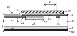
- FIG. 1 is a longitudinal sectional view showing an outline of a layer configuration in a silicon carbide semiconductor device according to a first embodiment of the present invention.
- FIG. 2 is a longitudinal sectional view showing an outline of a layer configuration in the silicon carbide semiconductor device according to the first modification of the first embodiment of the present invention.
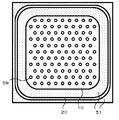
- FIG. 3 is an upper plan view of the silicon carbide semiconductor device according to the first embodiment of the present invention.
- FIG. 4 is an upper plan view of the silicon carbide semiconductor device according to the second modification of the first embodiment of the present invention.
- FIG. 5 is a longitudinal sectional view for illustrating the method for manufacturing the silicon carbide semiconductor device according to the first embodiment of the invention.
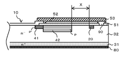
- FIG. 6 is a longitudinal sectional view showing an outline of a layer configuration in the silicon carbide semiconductor device according to the second embodiment of the present invention.
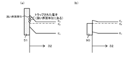
- FIG. 7A is a diagram for explaining the inversion layer
- FIG. 7B is a diagram for explaining the effect of the second electrode according to the second embodiment of the present invention.
- a silicon carbide semiconductor device is described as an example of a wide gap type semiconductor device.
- the present invention is not limited to this, and the present invention is also applied to other wide gap type semiconductor devices such as gallium nitride and gallium oxide. The invention can be used.
- the silicon carbide semiconductor device of the present embodiment is provided on a first conductivity type semiconductor substrate 31 and the first conductivity type semiconductor substrate 31, and is more first than the first conductivity type semiconductor substrate 31.
- the first conductivity type semiconductor layer 32 having a low conductivity type impurity concentration and inner peripheral second conductivity type regions 41 and 42 provided on the first conductivity type semiconductor layer 32 are provided.
- the inner peripheral second conductivity type regions 41 and 42 of the present embodiment are higher than the high concentration inner peripheral second conductivity type region 41 and the high concentration inner peripheral second conductivity type region 41. May also have a low concentration inner peripheral second conductivity type region 42 having a low second conductivity type impurity concentration.
- n-type is used as the “first conductivity type”
- p-type is used as the “second conductivity type”.
- the present invention is not limited to this mode, and the p-type may be used as the “first conductivity type” and the n-type may be used as the “second conductivity type”.
- the first conductive semiconductor substrate 31 has an upper surface as one main surface and a lower surface as the other main surface.
- the high concentration inner peripheral second conductivity type region 41 is located closer to the first electrode 10 (inner peripheral side) than the low concentration inner peripheral second conductivity type region 42.
- a low-concentration inner peripheral side second conductivity type region 42 may be provided so as to surround the inner peripheral side second conductivity type region 41.
- the depth of the low concentration inner peripheral side second conductivity type region 42 may be deeper than the depth of the high concentration inner peripheral side second conductivity type region 41.
- the width of the low concentration inner peripheral side second conductivity type region 42 may be wider than the width of the high concentration inner peripheral side second conductivity type region 41.
- the silicon carbide semiconductor device includes the first electrode 10, part of which is located on the inner periphery side second conductivity type regions 41, 42 and the remaining part is located on the first conductivity type semiconductor layer 32.
- the first electrode 10 may form a Schottky junction with the first conductivity type semiconductor layer 32.
- the inner peripheral second conductivity type regions 41 and 42 are located below the peripheral edge of the first electrode 10, and the inner peripheral second conductivity type regions 41 and 42 alleviate the electric field. It has a function.
- the silicon carbide semiconductor device is provided on the first conductivity type semiconductor layer 32 and adjacent to the first electrode 10, and the insulating layers 51, 52, extending to the end portion (right end in FIG. 1) of the silicon carbide semiconductor device. 53 and the outer peripheral side second conductivity type region 20 provided on the outer peripheral side of the inner peripheral side second conductivity type regions 41 and 42.
- the second conductivity type impurity concentration (p-type impurity concentration) in the outer peripheral second conductivity type region 20 is higher than the second conductivity type impurity concentration (p-type impurity concentration) in the low-concentration inner peripheral side second conductivity type region 42. It may be.
- the second conductivity type impurity concentration of the outer peripheral second conductivity type region 20 may be 1 ⁇ 10 18 to 1 ⁇ 10 23 , more specifically 1 ⁇ 10 19 to 1 ⁇ 10 23 . It may be.
- the “end portion of the silicon carbide semiconductor device” means a region near the end face of the silicon carbide semiconductor device.
- the distance X between the end portions of the inner periphery side second conductivity type regions 41 and 42 and the end portion of the outer periphery side second conductivity type region 20 is equal to the inner periphery side second conductivity type region 41. , 42 is larger than the depletion layer width extending from the outer peripheral side.
- the distance X may be 1.5 to 2 times larger than the value obtained by the above (formula 1).
- Equation 1 ⁇ s is the dielectric constant of the semiconductor, V bi is the built-in potential, and N d is the donor concentration.
- the distance X of the present embodiment is equal to the end of the low concentration inner peripheral second conductivity type region 42 (the right end of the low concentration inner peripheral second conductivity type region 42 in FIG. 1), It means the distance between the end portion of the outer peripheral second conductivity type region 20 (the left end of the contact surface in FIG. 1).
- the distance X between the end portions of the inner peripheral side second conductivity type regions 41 and 42 and the end portion of the outer peripheral side second conductivity type region 20 is from the end portion of the inner peripheral side second conductivity type regions 41 and 42 to the outer periphery. It may be larger than the sum of the width of the depletion layer extending to the side and the width of the depletion layer extending from the outer peripheral second conductivity type region 20 to the inner peripheral side.
- the theoretical depletion layer width extending from the outer peripheral side second conductivity type region 20 to the inner peripheral side is obtained by adding the second conductivity type impurity concentration of the outer peripheral side second conductivity type region 20 as the donor concentration in the above (Equation 1). It can be calculated by
- the outer peripheral side second conductivity type region 20 is arranged away from the end of the silicon carbide semiconductor device by a distance that does not cause damage when the silicon carbide semiconductor device is cut and manufactured (specifically, when dicing). May be. Since the damaged distance is 30 ⁇ m to 60 ⁇ m as an example, when this embodiment is adopted, the outer peripheral side second conductivity type region 20 extends from the end of the silicon carbide semiconductor device in the left-right direction in FIG. A distance of 30 ⁇ m to 60 ⁇ m or more is provided apart.
- the second conductivity type impurity concentration (p-type impurity concentration) in the high-concentration inner peripheral second conductivity type region 41 is equal to the second conductivity type impurity concentration (p-type impurity concentration) in the outer peripheral second conductivity type region 20. May be.
- the insulating layers 51, 52, and 53 of the present embodiment are formed on the first conductive semiconductor layer 32, the inner peripheral second conductive type regions 41 and 42, and the outer peripheral second conductive type region 20.
- the first insulating layer 51 provided on the first insulating layer 51 and the second insulating layer 52 provided on the first insulating layer 51 may be included.
- the outer peripheral second conductivity type region 20 may be provided below the second insulating layer 52.
- the third insulating layer 53 may be provided on the second insulating layer 52.
- the third insulating layer 53 may extend to the outer peripheral side (end portion side) than the second insulating layer 52 and may not extend to the end portion of the silicon carbide semiconductor device.
- the first insulating layer 51 can include a material containing PSG (Phosphorus Silicon Glass) and SiO 2
- the second insulating layer 52 can include a nitride film (for example, a material including SiN).
- a polyimide for example, a material containing high heat-resistant polyimide can be used as the third insulating layer 53.
- the thickness of the first insulating layer 51 is, for example, about 1 to 2 ⁇ m.
- the second insulating layer 52 may extend from any position above the inner peripheral second conductivity type regions 41 and 42 to at least the inner peripheral end of the outer peripheral second conductivity type region 20.
- the second insulating layer 52 is at least a central portion in the width direction of the outer peripheral second conductivity type region 20 from any position above the inner peripheral second conductivity type regions 41, 42. It may extend to. More specifically, the second insulating layer 52 extends from any position above the low-concentration inner peripheral side second conductivity type region 42 to at least the center of the outer peripheral side second conductivity type region 20 in the width direction. May be.
- the second insulating layer 52 extends from any position above the inner peripheral second conductivity type regions 41, 42 to at least the outer peripheral side end in the width direction of the outer peripheral second conductivity type region 20. Also good.
- the first insulating layer 51 located on the surface in the vicinity of the end face should reach the end of the semiconductor device in order to suppress discharge. In this case, the first insulating layer 51 reaches the end of the adjacent wide gap type semiconductor device (element) before the dicing division. It is sufficient that first insulating layer 51 extends to the extent that no discharge occurs between first electrode 10 and the end portion of the silicon carbide semiconductor device. For this reason, the area
- the third insulating layer 53 does not need to extend to the end face (the right end face in FIG. 1) of the first insulating layer 51 (it may not be provided on the end of the wide gap type semiconductor device).
- the material can be appropriately selected depending on the material applied to the third insulating layer 53 and the dicing division method.
- the first conductivity type impurity concentration (for example, nitrogen concentration) of the first conductivity type semiconductor substrate 31 is 5 ⁇ 10 17 cm ⁇ 3 to 5 ⁇ 10 19 , and the first conductivity type semiconductor layer 32 has the first conductivity type.
- the type impurity concentration may be 1 ⁇ 10 15 to 1 ⁇ 10 18 cm ⁇ 3 .
- the first conductive semiconductor substrate 31 may have a thickness of 30 ⁇ m to 400 ⁇ m, for example, and the first conductive semiconductor layer 32 may have a thickness of 3 ⁇ m to 20 ⁇ m, for example.
- the first electrode 10 may have a laminated structure using a plurality of types of metals. For example, titanium having a thickness of 0.5 ⁇ m and a thickness of 3 ⁇ m provided on the titanium, for example. You may have aluminum. Further, nickel may be provided on aluminum.
- the first electrode 10 and the first conductivity type semiconductor layer 32 of the present embodiment form a Schottky junction.
- the present invention is not limited to this, and as a modification, the first electrode 10 ′ and the first conductive type semiconductor layer 32 or the inner peripheral second conductive type regions 41 and 42 may form an ohmic junction.
- the high concentration inner peripheral second conductivity type region 41 is located below the first electrode 10 ′, and the high concentration inner peripheral second conductivity type region 41 and the first electrode 10 ′ Forms an ohmic junction. Further, as shown in FIG.
- an island-shaped p-type region 59 may be formed so as to form an island region in the first conductive type semiconductor layer 32, and the p-type region and the first electrode 10 are An ohmic junction may be formed, and the first conductivity type semiconductor layer 32 and the first electrode 10 may form a Schottky junction.
- one outer peripheral second conductivity type region 20 may be provided so as to surround part or all of the first electrode 10 continuously or intermittently (see FIG. 3). That is, in the present embodiment, a plurality of outer peripheral second conductivity type regions 20 are not provided, and only one outer peripheral second conductivity type region 20 may be provided. Of course, a plurality of outer peripheral second conductivity type regions 20 may be provided, and when a plurality of outer peripheral second conductivity type regions 20 are provided, a part of one outer peripheral second conductivity type region 20 or It may be provided such that another outer peripheral second conductivity type region 20 surrounds the whole continuously or intermittently. Further, the plurality of outer peripheral second conductivity type regions 20 may be provided at equal intervals from the center, may be provided so that the intervals are gradually narrowed, or may be provided so that the intervals are gradually increased. May be.
- the outer peripheral side second conductivity type region 20 When a part of the first electrode 10 is surrounded by the outer peripheral side second conductivity type region 20, a portion that is not surrounded by the outer peripheral side second conductivity type region 20 occurs on the outer periphery of the first electrode 10.
- the outer peripheral side second conductivity type region 20 surrounds the entire first electrode 10
- the entire first electrode 10 is continuously surrounded by the outer peripheral side second conductivity type region 20.
- the outer peripheral side second conductivity type region 20 continuously surrounds all of the first electrodes 10 as shown in FIG. 3 in a plan view (when viewed from above in FIG. 1). ), And the outer peripheral side second conductivity type region 20 continuously surrounds all of the first electrode 10.
- FIG. 1 the outer peripheral side second conductivity type region 20 continuously surrounds all of the first electrode 10.
- the outer peripheral side second conductivity type region 20 has a substantially hollow rectangular shape and surrounds the substantially rectangular first electrode 10.
- the mold region 20 may be, for example, a substantially circular shape with a hollow and may surround the first electrode 10.
- the silicon carbide semiconductor device of the present embodiment may have a back electrode 80 that is a back electrode on the back side of the first conductivity type semiconductor substrate 31 (the lower side in FIG. 1).
- the back electrode 80 forms, for example, an ohmic junction with the first conductivity type semiconductor substrate 31.
- the back electrode 80 may have a single-layer structure of nickel or a multilayer structure including nickel and titanium.
- a high-concentration first conductive semiconductor substrate 31 is prepared (see FIG. 5A).
- a low-concentration first conductive semiconductor layer 32 is formed by epitaxial growth on the high-concentration first conductive semiconductor substrate 31 (see FIG. 5A).
- the inner peripheral side second conductive type regions 41 and 42 including the low concentration inner peripheral side second conductive type region 42 and the high concentration inner peripheral side second conductive type region 41 and the outer peripheral side second conductive type region 20 are formed. (See FIG. 5B).
- a known method can be used. As an example, the following method can be used.
- a mask having openings at portions corresponding to the inner peripheral second conductivity type regions 41 and 42 and the outer peripheral second conductivity type region 20 is formed.
- p-type impurity ions for example, aluminum ions
- p-type impurity ions for example, aluminum ions
- the mask is removed.
- a mask having openings in portions corresponding to the high-concentration inner peripheral second conductivity type region 41 and the outer peripheral second conductivity type region 20 is formed.
- p-type impurity ions for example, aluminum ions
- the p-type impurity is activated by heating to a temperature of 1600 ° C. or higher.
- the first insulating layer 51 is provided on the first conductive type semiconductor layer 32 and the inner peripheral second conductive type regions 41 and 42. Thereafter, an opening for the first electrode 10 is formed at a position where a part of the first insulating layer 51 is located on the second conductivity type regions 41 and 42 and the remaining part is located on the first conductivity type semiconductor layer 32. (See FIG. 5B).
- buffer hydrofluoric acid can be used, for example.
- the first electrode 10 is provided in the first electrode 10 opening 51a (see FIG. 5C).
- a well-known method can be used also when providing the 1st electrode 10 in this way.
- an electrode containing titanium, nickel, and / or aluminum is provided by, for example, vapor deposition, chemical vapor deposition (CVD), coating / coating, electroplating, or the like.
- the first electrode 10 is formed so as to have the stepped portion 11 at the peripheral portion thereof.
- the second insulating layer 52 is provided on the first insulating layer 51 (see FIG. 5D). Thereafter, the third insulating layer 53 is provided so as to cover a part (peripheral portion) of the step-shaped portion 11 of the first electrode 10 and the entire second insulating layer 52.
- a back electrode 80 is formed on the lower surface (back surface) of the first conductivity type semiconductor substrate 31 (see FIG. 5D). Also in this case, the back electrode 80 can be formed by using a well-known method. For example, a metal containing nickel and / or titanium is formed by, for example, vapor deposition, chemical vapor deposition (CVD), coating / coating. It is provided by an electroplating method or the like.
- CVD chemical vapor deposition
- the first electrode 10 is heat-treated at an appropriate timing in the above-described process and at a predetermined temperature (for example, 500 ° C.) so as to form a Schottky junction with the first conductivity type semiconductor layer 32.
- heat treatment is performed at an appropriate timing in the above-described process and at a predetermined temperature (for example, 1000 ° C. or higher) so that the lower surface (back surface) of the first conductivity type semiconductor substrate 31 and the back electrode 80 form an ohmic junction. Done.
- the outer peripheral side second conductivity type region 20 is provided on the outer peripheral side of the inner peripheral side second conductivity type regions 41, 42, and the end portions of the inner peripheral side second conductivity type regions 41, 42 and The distance to the end of the outer peripheral second conductivity type region 20 is larger than the depletion layer width. For this reason, the effect different from a general guard ring can be acquired.
- the depletion layer can be expanded from the outer peripheral side second conductivity type region 20 to the outer peripheral side. As a result, the first electrode 10 And the vicinity of the end of the wide gap type semiconductor device can be prevented from generating discharge.
- the inner periphery side second conductivity type region 41 is connected in order to relax the electric field by connecting the depletion layer and gradually decreasing the anode potential.
- the end X of the outer peripheral side second conductivity type region 20 are designed such that the distance X is equal to or smaller than the depletion layer width.
- the outer peripheral second conductivity type region 20 of the present embodiment is not intended to connect the depletion layers.
- the distance X is It may be 1.5 times to 2 times or more the value obtained in (1).
- the distance X is it is possible to prevent the depletion layer from being unexpectedly connected.
- the distance X in the case of a silicon carbide Schottky barrier diode with a rated voltage of 1200 V, assuming that N d is 0.8 ⁇ 10 16 cm ⁇ 3 and applying a rated voltage of 1200 V, the distance X must be at least 12.9 ⁇ m. is there. In such a case, it is conceivable to design the distance X to about 18 ⁇ m to 25 ⁇ m (for example, 20 ⁇ m) from the viewpoint of preventing the depletion layer from being unexpectedly connected.
- insulating layers 51, 52, and 53 extend to the end of the silicon carbide semiconductor device, the first electrode 10 and the end of the silicon carbide semiconductor device Can be prevented from occurring between the two.
- the second conductivity type impurity concentration of the outer peripheral side second conductivity type region 20 is higher than the second conductivity type impurity concentration of the low concentration inner periphery side second conductivity type region 42 (reverse bias).
- a wide depletion layer can be generated from the outer peripheral second conductivity type region 20. For this reason, it can prevent more reliably that discharge generate
- the second conductivity type impurity concentration of the outer peripheral second conductivity type region 20 is low, the outer peripheral second conductivity type region 20 itself is depleted by the depletion layer spreading in the outer peripheral second conductivity type region 20. It can happen.
- the second conductivity type impurity concentration of the outer peripheral side second conductivity type region 20 is preferably 1 ⁇ 10 18 to 1 ⁇ 10 23 , and more preferably 1 ⁇ 10 19 to 1 ⁇ 10 23 .
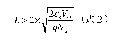
- the width L (see FIG. 1) of the outer peripheral second conductivity type region 20 only needs to satisfy the following formula.
- the reason why the depletion layer is doubled is that the depletion layer extends from both directions of the outer peripheral second conductivity type region. Since it is not preferable that the width L of the outer peripheral second conductivity type region 20 is increased, in order to reduce the width L of the outer peripheral second conductivity type region 20, the second in the outer peripheral side second conductivity type region 20 is used. it is necessary to increase the concentration N d of the conductive impurity.
- the interface state density at the interface between the insulating layers 51, 52, 53 and silicon carbide is larger than that at the interface between the insulating layers 51, 52, 53 and silicon (Si). Electrons are trapped by this interface state existing at the interface between the insulating layers 51, 52, 53 and the first conductivity type semiconductor layer 32 made of silicon carbide. Of the captured electrons, Since electrons at the interface state have a large time constant and cannot escape, they behave substantially as negative fixed charges (see FIG. 7A).
- the fixed charge is ⁇ 1 ⁇ 10 11 to ⁇ 1 ⁇ 10 13, which is larger than that of silicon.
- the band of the first conductivity type semiconductor layer 32 located immediately below the insulating layers 51, 52, and 53 is raised by the trapped electrons to be changed to the second conductivity type (the region having the second conductivity type is referred to as “ Inversion layer ").
- Such a phenomenon in the silicon carbide semiconductor device can also occur in a wide gap type semiconductor such as gallium nitride (GaN) or gallium oxide (Ga 2 O 3 ) other than silicon carbide.
- the second insulating layer 52 is at least on the inner peripheral side of the outer peripheral second conductive type region 20 from any position above the inner peripheral second conductive type regions 41 and 42.
- the inversion layer could be formed up to the outer peripheral second conductivity type region 20.
- the potential of the outer peripheral second conductivity type region 20 becomes almost the same value as the inner peripheral second conductivity type regions 41 and 42 by this inversion layer, and the depletion layer is sufficiently removed from the outer peripheral second conductivity type region 20. Can be spread. For this reason, it can prevent more reliably that discharge generate
- the effect of forming the inversion layer was remarkably shown when the second insulating layer 52 was a nitride film, and was particularly prominent when it was SiN. Therefore, it is very beneficial that the second insulating layer 52 is a nitride film (particularly SiN). Furthermore, since it has also been confirmed that this effect is sufficiently obtained when the second insulating layer 52 extends at least to the center in the width direction of the outer peripheral side second conductivity type region 20, It is beneficial to extend from any position above the inner peripheral second conductivity type regions 41 and 42 to at least the center of the outer peripheral side second conductivity type region 20 in the width direction. In addition, when the 2nd insulating layer 52 extended at least to the edge part of the outer peripheral side of the width direction of the outer peripheral side 2nd conductivity type area
- the inversion layer is formed to the end of the wide gap type semiconductor device by providing the outer peripheral side second conductivity type region 20 and / or the second insulating layer 52 (which is a nitride film) does not extend to the end. Can be prevented. As a result, leakage current can be prevented from being generated by the inversion layer.
- the outer periphery side second conductivity type region 20 When the outer periphery side second conductivity type region 20 is disposed away from the end of the wide gap type semiconductor device by a distance that does not cause damage when the wide gap type semiconductor device is cut and manufactured. Can prevent the depletion layer extending from the outer peripheral second conductivity type region 20 from touching such damage. This is because an electric field is generated in the depletion layer, and if the depletion layer touches such damage, a leakage current is generated. From this point of view, the outer peripheral second conductivity type region 20 has a distance (30 ⁇ m to 60 ⁇ m or more) that does not cause damage when the wide gap type semiconductor device is cut from the end of the wide gap type semiconductor device. It is more advantageous to arrange them apart from the “sum” of the width of the depletion layer extending from the outer peripheral second conductivity type region 20 to the outer peripheral side.
- the distance X between the end portions of the inner peripheral second conductivity type regions 41 and 42 and the end portion of the outer peripheral second conductivity type region 20 is the end portion of the inner peripheral second conductivity type regions 41 and 42.
- the inner periphery side second conductivity type region It is possible to prevent the depletion layer extending from the end portions of 41 and 42 to the outer peripheral side from overlapping with the depletion layer extending from the outer peripheral second conductivity type region 20 to the inner peripheral side, thereby preventing the influence of both.
- the design content regarding the inner peripheral side second conductivity type regions 41 and 42 for withstand voltage can be used when designing other semiconductor devices, and the outer peripheral side second for preventing discharge.
- the design content regarding the conductivity type region 20 can be used when designing another semiconductor device.
- the already acquired data can be made versatile.
- the first component including the inner peripheral second conductivity type regions 41 and 42 and the second component including the outer peripheral second conductivity type region 20 are manufactured separately, and a semiconductor device is manufactured by appropriately combining them. You can also
- the design for realizing the withstand voltage is complicated, and therefore, when the guard ring is affected by the outer peripheral side second conductivity type region 20, the design is performed. Reworking is very time consuming. For this reason, the distance (distance in the left-right direction in FIG. 1) between the end of the outer peripheral second conductivity type region 20 and the pressure-resistant structure such as the guard ring is the inner distance from the end of the outer peripheral second conductivity type region 20. It is beneficial that the depletion layer extending on the peripheral side does not overlap with the depletion layer extending on the outer peripheral side from the pressure-resistant structure.
- the second conductivity type impurity concentration in the high concentration inner peripheral side second conductivity type region 41 is equal to the second conductivity type impurity concentration in the outer periphery side second conductivity type region 20
- the high concentration Since the inner periphery side second conductivity type region 41 and the outer periphery side second conductivity type region 20 can be manufactured by the same method, the manufacturing process can be simplified and the manufacturing cost can be reduced.
- the depletion layer can be expanded evenly when viewed from above. It is beneficial in that it can be done. Even when only one outer peripheral second conductivity type region 20 is provided, it is sufficient as an effect of suppressing discharge from the first electrode 10 to the end of the wide gap semiconductor device (element). Note that you can expect to get
- the outer peripheral side second conductivity type region 20 may be provided intermittently so as to surround the first electrode 10, or provided so as to surround only a part of the first electrode 10. May be.
- a second Schottky junction is formed with the first conductivity type semiconductor layer 32 on the outer peripheral side (end portion side) than the outer peripheral second conductivity type region 20.
- An electrode 90 is provided.
- the second electrode 90 is provided between the outer peripheral second conductivity type region 20 and the end of the wide gap type semiconductor device, and the second electrode 90 and the first conductivity type semiconductor layer 32 are connected to each other.
- a Schottky junction is formed. For this reason, it is possible to prevent the “inversion layer” that has passed through the outer peripheral side second conductivity type region 20 from being formed on the outer peripheral side of the second electrode 90 without trapping electrons and raising the band at the position (FIG. 7). (See (b)). As a result, it is possible to more reliably prevent leakage current from being generated by the inversion layer.
- the discharge between the first electrode 10 and the second electrode 90 can be suppressed.
Landscapes
- Electrodes Of Semiconductors (AREA)
Abstract
ワイドギャップ型半導体装置は、第1導電型半導体層32と、前記第1導電型半導体層32上に設けられた内周側第2導電型領域41,42と、第1電極10と、前記第1導電型半導体層32上であって前記第1電極10に隣接して設けられ、前記ワイドギャップ型半導体装置の端部まで延びた絶縁層51,52,53と、前記内周側第2導電型領域41,42の外周側に設けられた外周側第2導電型領域20と、を有している。前記内周側第2導電型領域41,42の端部と前記外周側第2導電型領域20の端部との間の距離は、前記内周側第2導電型領域41,42から外周側に広がる空乏層幅より大きくなっている。
Description
本発明は、ワイドギャップ型半導体装置に関する。
近年、様々な利点があることから炭化ケイ素半導体装置等のワイドギャップ型半導体装置が注目を集めている。しかしながら、このようなワイドギャップ型半導体装置において、アクティブ領域に形成される電極又は配線からワイドギャップ型半導体装置の端部までの距離が短くなった場合では、サージ電圧のような負電圧がワイドギャップ型半導体装置の表面側の電極に印加されると、電極とワイドギャップ型半導体装置の端部との間において放電が起こるという問題がある(特開2009-231321号公報)。
これを防止するために、ワイドギャップ型半導体装置の第1導電型半導体層の表面を絶縁層(絶縁膜を含む)によって完全に覆うことが考えられるが、このような態様でも十分に放電を抑制することができなかった。
本発明はこのような観点からなされたものであり、放電を十分に抑制できるワイドギャップ型半導体装置を提供する。
本発明によるワイドギャップ型半導体装置は、
第1導電型半導体層と、
前記第1導電型半導体層上に設けられた内周側第2導電型領域と、
一部が前記内周側第2導電型領域上に位置し、残部が前記第1導電型半導体層上に位置する第1電極と、
前記第1導電型半導体層上であって前記第1電極に隣接して設けられ、前記ワイドギャップ型半導体装置の端部まで延びた絶縁層と、
前記第1導電型半導体層上であって、前記内周側第2導電型領域の外周側に設けられた外周側第2導電型領域と、
を備え、
前記内周側第2導電型領域の端部と前記外周側第2導電型領域の端部との間の距離は、前記内周側第2導電型領域から外周側に広がる空乏層幅より大きくなっている。
第1導電型半導体層と、
前記第1導電型半導体層上に設けられた内周側第2導電型領域と、
一部が前記内周側第2導電型領域上に位置し、残部が前記第1導電型半導体層上に位置する第1電極と、
前記第1導電型半導体層上であって前記第1電極に隣接して設けられ、前記ワイドギャップ型半導体装置の端部まで延びた絶縁層と、
前記第1導電型半導体層上であって、前記内周側第2導電型領域の外周側に設けられた外周側第2導電型領域と、
を備え、
前記内周側第2導電型領域の端部と前記外周側第2導電型領域の端部との間の距離は、前記内周側第2導電型領域から外周側に広がる空乏層幅より大きくなっている。
本発明によるワイドギャップ型半導体装置において、
前記外周側第2導電型領域は、前記ワイドギャップ型半導体装置の端部から、前記ワイドギャップ型半導体装置を切断して製造する際に入るダメージを受けない距離だけ離れて配置されてもよい。
前記外周側第2導電型領域は、前記ワイドギャップ型半導体装置の端部から、前記ワイドギャップ型半導体装置を切断して製造する際に入るダメージを受けない距離だけ離れて配置されてもよい。
本発明によるワイドギャップ型半導体装置において、
前記内周側第2導電型領域は、高濃度内周側第2導電型領域と、前記高濃度内周側第2導電型領域よりも第2導電型不純物濃度が低い低濃度内周側第2導電型領域とを有し、
前記外周側第2導電型領域の第2導電型不純物濃度は、前記低濃度内周側第2導電型領域の第2導電型不純物濃度よりも高くなってもよい。
前記内周側第2導電型領域は、高濃度内周側第2導電型領域と、前記高濃度内周側第2導電型領域よりも第2導電型不純物濃度が低い低濃度内周側第2導電型領域とを有し、
前記外周側第2導電型領域の第2導電型不純物濃度は、前記低濃度内周側第2導電型領域の第2導電型不純物濃度よりも高くなってもよい。
本発明によるワイドギャップ型半導体装置において、
前記高濃度内周側第2導電型領域における第2導電型不純物濃度は、前記外周側第2導電型領域における第2導電型不純物濃度と等しくなってもよい。
前記高濃度内周側第2導電型領域における第2導電型不純物濃度は、前記外周側第2導電型領域における第2導電型不純物濃度と等しくなってもよい。
本発明によるワイドギャップ型半導体装置において、
前記絶縁層は、前記第1導電型半導体層上に設けられた第1絶縁層と、前記第1絶縁層上に設けられた第2絶縁層とを有し、
前記第2絶縁層は、前記内周側第2導電型領域の上方のいずれかの位置から少なくとも前記外周側第2導電型領域の内周側端部まで延びてもよい。
前記絶縁層は、前記第1導電型半導体層上に設けられた第1絶縁層と、前記第1絶縁層上に設けられた第2絶縁層とを有し、
前記第2絶縁層は、前記内周側第2導電型領域の上方のいずれかの位置から少なくとも前記外周側第2導電型領域の内周側端部まで延びてもよい。
本発明によるワイドギャップ型半導体装置において、
前記第2絶縁層が窒化膜であってもよい。
前記第2絶縁層が窒化膜であってもよい。
本発明によるワイドギャップ型半導体装置において、
前記第2絶縁層は、前記内周側第2導電型領域の上方のいずれかの位置から少なくとも前記外周側第2導電型領域の幅方向の中心部まで延びてもよい。
前記第2絶縁層は、前記内周側第2導電型領域の上方のいずれかの位置から少なくとも前記外周側第2導電型領域の幅方向の中心部まで延びてもよい。
本発明によるワイドギャップ型半導体装置において、
前記絶縁層は、前記第2絶縁層上に設けられた第3絶縁層をさらに有し、
前記第3絶縁層は、前記第2絶縁層よりも外周側に延びるとともに、前記ワイドギャップ型半導体装置の端部まで延びていなくてもよい。
前記絶縁層は、前記第2絶縁層上に設けられた第3絶縁層をさらに有し、
前記第3絶縁層は、前記第2絶縁層よりも外周側に延びるとともに、前記ワイドギャップ型半導体装置の端部まで延びていなくてもよい。
本発明によるワイドギャップ型半導体装置において、
前記内周側第2導電型領域の端部と前記外周側第2導電型領域の端部との間の距離は、前記内周側第2導電型領域の端部から外周側に広がる空乏層幅と、外周側第2導電型領域から内周側に広がる空乏層幅との和よりも大きくなってもよい。
前記内周側第2導電型領域の端部と前記外周側第2導電型領域の端部との間の距離は、前記内周側第2導電型領域の端部から外周側に広がる空乏層幅と、外周側第2導電型領域から内周側に広がる空乏層幅との和よりも大きくなってもよい。
本発明によるワイドギャップ型半導体装置は、
前記外周側第2導電型領域よりも外周側に設けられ、前記第1導電型半導体層とショットキー接合を形成する第2電極をさらに備えてもよい。
前記外周側第2導電型領域よりも外周側に設けられ、前記第1導電型半導体層とショットキー接合を形成する第2電極をさらに備えてもよい。
本発明によれば、内周側第2導電型領域の外周側に外周側第2導電型領域が設けられ、内周側第2導電型領域の端部と外周側第2導電型領域の端部との間の距離が空乏層幅より大きくなっている。本発明のような外周側第2導電型領域を用いることで、外周側第2導電型領域から外周側に空乏層を広げることができ、その結果、第1電極とワイドギャップ型半導体装置の端部近辺との間で放電が発生することを防止できる。
第1の実施の形態
《構成》
本実施の形態では、ワイドギャップ型半導体装置の一例として炭化ケイ素半導体装置を用いて説明するが、これに限られることはなく、例えば窒化ガリウム、酸化ガリウムといった他のワイドギャップ型半導体装置にも本発明を用いることができる。
《構成》
本実施の形態では、ワイドギャップ型半導体装置の一例として炭化ケイ素半導体装置を用いて説明するが、これに限られることはなく、例えば窒化ガリウム、酸化ガリウムといった他のワイドギャップ型半導体装置にも本発明を用いることができる。
図1に示すように、本実施の形態の炭化ケイ素半導体装置は、第1導電型半導体基板31と、第1導電型半導体基板31上に設けられ、第1導電型半導体基板31よりも第1導電型不純物濃度の低い第1導電型半導体層32と、第1導電型半導体層32上に設けられた内周側第2導電型領域41,42と、を有している。
図1に示すように、本実施の形態の内周側第2導電型領域41,42は、高濃度内周側第2導電型領域41と、高濃度内周側第2導電型領域41よりも第2導電型不純物濃度が低い低濃度内周側第2導電型領域42とを有してもよい。
本実施の形態では、以下、「第1導電型」としてn型を用いて説明し、「第2導電型」としてp型を用いて説明する。但し、このような態様に限られることはなく、「第1導電型」としてp型を用い、「第2導電型」としてn型を用いてもよい。なお、本実施の形態において、第1導電型半導体基板31は、その上方側の面が一方の主面となり下方側の面が他方の主面となっている。
図1の左右方向において、高濃度内周側第2導電型領域41は低濃度内周側第2導電型領域42よりも第1電極10側(内周側)に位置しており、高濃度内周側第2導電型領域41を取り囲むようにして低濃度内周側第2導電型領域42が設けられてもよい。また、低濃度内周側第2導電型領域42の深さは高濃度内周側第2導電型領域41の深さよりも深くなってもよい。低濃度内周側第2導電型領域42の幅は高濃度内周側第2導電型領域41の幅よりも広くなってもよい。
炭化ケイ素半導体装置は、一部が内周側第2導電型領域41,42上に位置し、残部が第1導電型半導体層32上に位置する第1電極10を有している。第1電極10は第1導電型半導体層32とショットキー接合を形成してもよい。本実施の形態では、この第1電極10の周縁部下方に内周側第2導電型領域41,42が位置しており、この内周側第2導電型領域41,42は電界を緩和する機能を有している。炭化ケイ素半導体装置は、第1導電型半導体層32上であって第1電極10に隣接して設けられ、炭化ケイ素半導体装置の端部(図1の右端)まで延びた絶縁層51,52,53と、内周側第2導電型領域41,42の外周側に設けられた外周側第2導電型領域20と、を有している。
外周側第2導電型領域20の第2導電型不純物濃度(p型不純物濃度)は、低濃度内周側第2導電型領域42の第2導電型不純物濃度(p型不純物濃度)よりも高くなってもよい。一例として、外周側第2導電型領域20の第2導電型不純物濃度は、1×10¹⁸~1×10²³となってもよく、より具体的には1×10¹⁹~1×10²³となってもよい。
本実施の形態において「炭化ケイ素半導体装置の端部」とは炭化ケイ素半導体装置の端面近辺領域のことを意味している。この端面近辺領域の表面が絶縁層51,52,53で覆われていない状態で負の高電圧を印加すると、第1電極10から放出された電子が、この端面近辺領域に落雷しやすくなる。すなわち、「放電」が起こりやすくなる。
本実施の形態では、内周側第2導電型領域41,42の端部と、外周側第2導電型領域20の端部との間の距離Xは、内周側第2導電型領域41,42から外周側に広がる空乏層幅より大きくなっている。内周側第2導電型領域41,42から外周側に広がる理論的な空乏層幅としては、例えば、
 を挙げることができる。距離Xを理論的な空乏層幅よりも大きくする場合には、距離Xを上記(式1)で得られる値の1.5倍~2倍以上の大きさとしてもよい。なお、(式1)において、εsは半導体の誘電率であり、Vbiは内蔵電位であり、Ndはドナー濃度である。
より具体的には、本実施の形態の上記距離Xは、低濃度内周側第2導電型領域42の端部(図1における低濃度内周側第2導電型領域42の右端)と、外周側第2導電型領域20の端部(図1における当該接触面の左端)との間の距離を意味している。
内周側第2導電型領域41,42の端部と外周側第2導電型領域20の端部との間の距離Xは、内周側第2導電型領域41,42の端部から外周側に広がる空乏層幅と、外周側第2導電型領域20から内周側に広がる空乏層幅との和よりも大きくなっていてもよい。外周側第2導電型領域20から内周側に広がる理論的な空乏層幅は、上記(式1)において、ドナー濃度として外周側第2導電型領域20の第2導電型不純物濃度を入れることで算出できる。
外周側第2導電型領域20は、炭化ケイ素半導体装置の端部から、炭化ケイ素半導体装置を切断して製造する際(具体的にはダイシングする際)に入るダメージを受けない距離だけ離れて配置されてもよい。ダメージを受けている距離は一例としては30μm~60μmであるので、この態様を採用する場合には、外周側第2導電型領域20は、炭化ケイ素半導体装置の端部から図1の左右方向で30μm~60μm以上の距離が離されて設けられることになる。
高濃度内周側第2導電型領域41における第2導電型不純物濃度(p型不純物濃度)は、外周側第2導電型領域20における第2導電型不純物濃度(p型不純物濃度)と等しくなってもよい。
本実施の形態の絶縁層51,52,53は、図1に示すように、第1導電型半導体層32、内周側第2導電型領域41,42及び外周側第2導電型領域20上に設けられた第1絶縁層51と、第1絶縁層51上に設けられた第2絶縁層52とを有してもよい。第2絶縁層52の下方に、外周側第2導電型領域20が設けられてもよい。
また、第2絶縁層52上に第3絶縁層53が設けられてもよい。この第3絶縁層53は、第2絶縁層52よりも外周側(端部側)に延びるとともに、炭化ケイ素半導体装置の端部まで延びていなくてもよい。
一例としては、第1絶縁層51としてはPSG(Phosphorus Silicon Glass)及びSiO2を含むものを用いることができ、第2絶縁層52としては窒化膜(例えばSiNを含むもの。)を用いることができ、第3絶縁層53としてはポリイミド、例えば高耐熱ポリイミドを含むものを用いることができる。なお、第1絶縁層51の厚みは例えば1~2μm程である。
第2絶縁層52は、内周側第2導電型領域41,42の上方のいずれかの位置から少なくとも外周側第2導電型領域20の内周側端部まで延びていてもよい。また、この態様の一例としては、第2絶縁層52は、内周側第2導電型領域41,42の上方のいずれかの位置から少なくとも外周側第2導電型領域20の幅方向の中心部まで延びていてもよい。より具体的には、第2絶縁層52は、低濃度内周側第2導電型領域42の上方のいずれかの位置から少なくとも外周側第2導電型領域20の幅方向の中心部まで延びていてもよい。また、第2絶縁層52は、内周側第2導電型領域41,42の上方のいずれかの位置から少なくとも外周側第2導電型領域20の幅方向の外周側の端部まで延びていてもよい。
端面近辺領域の表面上に位置する第1絶縁層51は放電を抑制するために、半導体装置端部まで達している方がよい。この場合には、ダイシング分割前においては、第1絶縁層51は隣接するワイドギャップ型半導体装置(素子)の端部に達することになる。なお、第1絶縁層51は第1電極10と炭化ケイ素半導体装置の端部との間で放電が発生しない程度まで延びていれば足りる。このため、わずかに第1絶縁層51が設けられていない領域が炭化ケイ素半導体装置の端面近辺に存在してもよい。
第3絶縁層53は第1絶縁層51の端面(図1の右端面)まで延びている必要はない(ワイドギャップ型半導体装置の端部上には設けられていなくてもよい。)。一例として第3絶縁層53がワイドギャップ型半導体装置の端部まで達する設計で、かつ粘性の大きいポリイミド樹脂を用いる場合、ダイシング分割の際、装置をチョコ停止させる原因となる。このため、生産性を考慮すると第3絶縁層53はワイドギャップ型半導体装置の端部まで達していない方がよい場合もある。この点、第3絶縁層53に適用する材質や、ダイシング分割の方法によって適宜選択できる。
一例ではあるが、第1導電型半導体基板31の第1導電型不純物濃度(例えば窒素濃度)は5×1017cm-3~5×10¹⁹となり、第1導電型半導体層32の第1導電型不純物濃度は1×10¹⁵~1×1018cm-3となってもよい。また、第1導電型半導体基板31は例えば30μ~400μmの厚さとなり、第1導電型半導体層32は例えば3μm~20μmの厚さとなってもよい。また、第1電極10は、複数種類の金属を用いた積層構造となっていてもよく、例えば0.5μmの厚さであるチタンと、当該チタンの上に設けられた例えば3μmの厚さのアルミニウムとを有してもよい。また、アルミニウムの上にニッケルを設けてもよい。
本実施の形態の第1電極10と第1導電型半導体層32とはショットキー接合を形成している。しかしながら、これに限られることはなく、変形例としては、第1電極10’と第1導電型半導体層32又は内周側第2導電型領域41,42とがオーミック接合を形成してもよい。図2に示す態様では、高濃度内周側第2導電型領域41が第1電極10’の下方に位置しており、高濃度内周側第2導電型領域41と第1電極10’とがオーミック接合を形成している。また、図4に示すように、第1導電型半導体層32内に島領域を形成するようにして島状p型領域59が形成されてもよく、このp型領域と第1電極10とはオーミック接合を形成し、第1導電型半導体層32と第1電極10とはショットキー接合を形成するようになっていてもよい。
本実施の形態では、第1電極10の一部又は全体を連続的又は断続的に取り囲むようにして、1つの外周側第2導電型領域20が設けられてもよい(図3参照)。つまり、本実施の形態では複数の外周側第2導電型領域20が設けられてはおらず、1つの外周側第2導電型領域20だけが設けられてもよい。もちろん、複数の外周側第2導電型領域20が設けられてもよく、複数の外周側第2導電型領域20が設けられる場合には、一の外周側第2導電型領域20の一部又は全体を別の外周側第2導電型領域20が連続的又は断続的に取り囲むようにして設けられてもよい。また、複数の外周側第2導電型領域20は中心部から等間隔に設けられてもよいし、徐々に間隔が狭まるようにして設けられてもよいし、徐々に間隔が広がるようにして設けられてもよい。
第1電極10の一部を外周側第2導電型領域20が取り囲む場合には、第1電極10の外周には外周側第2導電型領域20によって取り囲まれない部分が発生する。他方、第1電極10の全部を外周側第2導電型領域20が取り囲む場合には、第1電極10の全てが外周側第2導電型領域20によって連続的に取り囲まれることになる。本実施の形態において、第1電極10の全てを外周側第2導電型領域20が連続的に取り囲むというのは、図3に示すように、平面図において(図1の上方から見た場合において)、第1電極10の全てを外周側第2導電型領域20が連続的に取り囲んでいることを意味する。図3では、説明の便宜上、第1電極10、外周側第2導電型領域20及び第1絶縁層51だけを示しており、第2絶縁層52、第3絶縁層53、内周側第2導電型領域41,42等は示していない。なお、図3では、外周側第2導電型領域20が中抜きの略矩形状となり、略矩形状の第1電極10を取り囲んでいるが、これに限られることはなく、外周側第2導電型領域20は例えば中抜きの略円形状となって、第1電極10を取り囲んでもよい。
本実施の形態の炭化ケイ素半導体装置は、第1導電型半導体基板31の裏面側(図1の下方側)に、裏面側電極である裏面電極80を有してもよい。この裏面電極80は、例えば第1導電型半導体基板31とオーミック接合を形成している。裏面電極80は例えばニッケルの単層構造となってもよいし、ニッケルとチタンを含む多層構造からなってもよい。
≪製造方法≫
次に、上述した構成からなる炭化ケイ素半導体装置の製造方法の概略を説明する。ここでは第1電極10が第1導電型半導体層32とショットキー接合を形成する態様について説明するが、あくまでも一例であることには留意が必要である。なお、「製造方法」で説明するあらゆる態様を上記「構成」で採用することができ、逆に、上記「構成」のあらゆる態様を「製造方法」で採用することができる。
次に、上述した構成からなる炭化ケイ素半導体装置の製造方法の概略を説明する。ここでは第1電極10が第1導電型半導体層32とショットキー接合を形成する態様について説明するが、あくまでも一例であることには留意が必要である。なお、「製造方法」で説明するあらゆる態様を上記「構成」で採用することができ、逆に、上記「構成」のあらゆる態様を「製造方法」で採用することができる。
まず、高濃度の第1導電型半導体基板31を準備する(図5(a)参照)。
次に、高濃度の第1導電型半導体基板31上に、エピタキシャル成長によって低濃度の第1導電型半導体層32を形成する(図5(a)参照)。
次に、低濃度内周側第2導電型領域42及び高濃度内周側第2導電型領域41を含む内周側第2導電型領域41,42と外周側第2導電型領域20を形成する(図5(b)参照)。このように内周側第2導電型領域41,42及び外周側第2導電型領域20を形成し活性化する際には、周知の方法を用いることができる。一例としては、以下に述べるような方法を用いることができる。まず、内周側第2導電型領域41,42及び外周側第2導電型領域20に対応する部分に開口を有するマスクを形成する。その後、当該マスクを介して、第1導電型半導体層32の所定部位にp型不純物イオン(例えば、アルミニウムイオン)を、多段階に分けて、比較的高エネルギー量でかつ比較的少量打ち込む。その後、マスクを除去する。次に、高濃度内周側第2導電型領域41及び外周側第2導電型領域20に対応する部分に開口を有するマスクを形成する。その後、当該マスクを介して第1導電型半導体層32の所定部位にp型不純物イオン(例えば、アルミニウムイオン)を、多段階に分けて、比較的低エネルギー量でかつ多量打ち込む。その後、マスクを除去する。そして、例えば1600℃以上の温度に加熱することでp型不純物を活性化させる。
次に、第1導電型半導体層32及び内周側第2導電型領域41,42上に第1絶縁層51を設ける。その後で、第1絶縁層51のうち、一部が第2導電型領域41,42上に位置し残部が第1導電型半導体層32上に位置する位置に第1電極10用開口部を形成する(図5(b)参照)。なお、このように第1電極10用開口部51を形成する際には、例えば緩衝フッ酸を用いることができる。
次に、第1電極10用開口部51a内に第1電極10を設ける(図5(c)参照)。このように第1電極10を設ける際にも、周知の方法を用いることができる。一例を挙げると、チタン、ニッケル及び/又はアルミニウム等を含む電極が、例えば蒸着、化学気相成長法(CVD法)、塗布・コーティング法、電気メッキ法等によって設けられる。この際、第1電極10は、その周縁部に段形状部11を有するようにして形成される。
次に、第1絶縁層51上に第2絶縁層52が設けられる(図5(d)参照)。その後で、第1電極10の段形状部11の一部(周縁部)及び第2絶縁層52の全部を覆うようにして第3絶縁層53が設けられる。
第1導電型半導体基板31の下面(裏面)には裏面電極80が形成される(図5(d)参照)。この際にも周知の方法を用いて裏面電極80を形成することができ、例えば、ニッケル及び/又はチタン等を含む金属が、例えば蒸着、化学気相成長法(CVD法)、塗布・コーティング法、電気メッキ法等によって設けられる。
第1電極10は第1導電型半導体層32とショットキー接合を形成するように、前述した工程内の適宜のタイミングかつ所定の温度(例えば500℃)で加熱処理が行われる。また、第1導電型半導体基板31の下面(裏面)と裏面電極80とがオーミック接合を形成するように、前述した工程内の適宜のタイミングかつ所定の温度(例えば1000℃以上)で加熱処理が行われる。
《作用・効果》
次に、上述した構成からなる本実施の形態による作用・効果のうち、まだ説明していないものについて説明する。なお、「作用・効果」で説明するあらゆる態様を、上記「構成」で採用することができる。
次に、上述した構成からなる本実施の形態による作用・効果のうち、まだ説明していないものについて説明する。なお、「作用・効果」で説明するあらゆる態様を、上記「構成」で採用することができる。
本実施の形態によれば、内周側第2導電型領域41,42の外周側に外周側第2導電型領域20が設けられ、内周側第2導電型領域41,42の端部と外周側第2導電型領域20の端部との間の距離が空乏層幅より大きくなっている。このため、一般的なガードリングとは異なる効果を得ることができる。具体的には、本発明のような外周側第2導電型領域20を用いることで、外周側第2導電型領域20から外周側に空乏層を広げることができ、その結果、第1電極10とワイドギャップ型半導体装置の端部近辺との間で放電が発生することを防止できる。
なお仮に外周側第2導電型領域20をガードリングとして機能させるのであれば、空乏層を繋げてアノード電位を徐々に小さくすることによって電界を緩和するために、内周側第2導電型領域41,42の端部と外周側第2導電型領域20の端部との間の距離Xは空乏層幅以下となるようにして設計される。しかしながら、本実施の形態の外周側第2導電型領域20は、空乏層を繋げることを目的とはしていない。
製造誤差やその他の要因も鑑みると、上記距離Xを
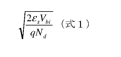 で得られる値の1.5倍~2倍以上の大きさとしてもよい。このような態様を採用することで、予期せず空乏層が繋がってしまうということを防止することができる。例えば、定格電圧1200Vの炭化ケイ素ショットキーバリアダイオードの場合、Ndが0.8×1016cm-3だとして、定格電圧1200Vを印加する場合は、距離Xは最低でも12.9μmは必要である。このような場合には、予期せず空乏層が繋がってしまうということを防止する観点から、距離Xを18μm~25μm(一例としては20μm)程度に設計することが考えられる。
また、本実施の形態によれば、図1に示すように絶縁層51,52,53が炭化ケイ素半導体装置の端部まで延びていることから第1電極10と炭化ケイ素半導体装置の端部との間で放電が発生することを防止できる。
また、外周側第2導電型領域20の第2導電型不純物濃度が低濃度内周側第2導電型領域42の第2導電型不純物濃度よりも高い態様を採用した場合には、(逆バイアス時に)外周側第2導電型領域20から幅の広い空乏層を発生させることができる。このため、第1電極10とワイドギャップ型半導体装置の端部近辺との間で放電が発生することをより確実に防止できる。なお、外周側第2導電型領域20の第2導電型不純物濃度が低い場合には、外周側第2導電型領域20内に広がる空乏層によって外周側第2導電型領域20自身が空乏化してしまうことが起こりうる。このように外周側第2導電型領域20自身が空乏化してしまうと、それ以上には外周側第2導電型領域20の外周及び内周側には空乏層が広がらない。他方、外周側第2導電型領域20の第2導電型不純物濃度が高い場合には、外周側第2導電型領域20自身が空乏化してしまうことが起こりにくい。このため、外周側第2導電型領域20の外周及び内周側に広い空乏層を形成できる。この観点からすると、第2導電型不純物濃度は、1×10¹⁸~1×10²³であることが好ましく、1×10¹⁹~1×10²³であることがより好ましい。
なお、外周側第2導電型領域20自身が空乏化しないようにするためには、外周側第2導電型領域20の幅L(図1参照)が、以下の数式を満たせばよい。なお、2倍されているのは、外周側第2導電型領域の両方向から空乏層が内部に広がるためである。外周側第2導電型領域20の幅Lが大きくなることはあまり好ましくないことから、外周側第2導電型領域20の幅Lを小さくするためには外周側第2導電型領域20における第2導電型不純物の濃度Ndを高くする必要がある。
絶縁層51,52,53と炭化ケイ素からなる第1導電型半導体層32との間の界面には、界面準位が存在している。特に、絶縁層51,52,53と炭化ケイ素との間の界面における界面準位密度は絶縁層51,52,53とケイ素(Si)との間の界面と比較して大きくなっている。絶縁層51,52,53と炭化ケイ素からなる第1導電型半導体層32との間の界面に存在するこの界面準位によって電子がトラップされることになるが、捕えられた電子のうち、深い界面準位にある電子は時定数が大きく脱出できないので、実質的には負の固定電荷として振る舞う(図7(a)参照)。特に、炭化ケイ素はケイ素よりもバンドギャップが大きいため、固定電荷は-1×10¹¹~-1×10¹³とケイ素の場合と比較して大きくなってしまう。このため、絶縁層51,52,53の直下に位置する第1導電型半導体層32は、トラップされた電子によってバンドが持ち上がり、第2導電型化する(この第2導電型化した領域を「反転層」という。)。このような炭化ケイ素半導体装置における現象は、炭化ケイ素以外の窒化ガリウム(GaN)、酸化ガリウム(Ga2O3)といったワイドギャップ型半導体でも生じうる。
そして、本願の発明者らの研究によって、当該第2絶縁層52が内周側第2導電型領域41,42の上方のいずれかの位置から少なくとも外周側第2導電型領域20の内周側端部まで延びている場合には、反転層が外周側第2導電型領域20まで形成できることを確認できた。この結果、この反転層によって外周側第2導電型領域20の電位は内周側第2導電型領域41,42とほぼ同じ値になり、外周側第2導電型領域20から空乏層を十分に広げることができる。このため、第1電極10と炭化ケイ素半導体装置の端部との間で放電が発生することをより確実に防止できる。
反転層が形成される効果は、第2絶縁層52が窒化膜である場合に顕著に示されることも確認でき、特にSiNである場合により顕著に示されることを確認できた。このため、第2絶縁層52は窒化膜(特にSiN)であることが非常に有益である。さらに、第2絶縁層52が少なくとも外周側第2導電型領域20の幅方向の中心部まで延びている場合に、この効果を十分に得ることも確認できたので、第2絶縁層52は、内周側第2導電型領域41,42の上方のいずれかの位置から少なくとも外周側第2導電型領域20の幅方向の中心部まで延びていることが有益である。なお、第2絶縁層52が少なくとも外周側第2導電型領域20の幅方向の外周側の端部まで延びている場合には、より十分な効果を得ることができた。
外周側第2導電型領域20が設けられること及び/又は(窒化膜である)第2絶縁層52が端部まで延びないことで、反転層がワイドギャップ型半導体装置の端部まで形成されることを防止できる。この結果、反転層によって漏れ電流が発生することを防止できる。
外周側第2導電型領域20がワイドギャップ型半導体装置の端部からワイドギャップ型半導体装置を切断して製造する際に入るダメージを受けない距離だけ離れて配置されている態様を採用した場合には、外周側第2導電型領域20から広がる空乏層がこのようなダメージに触れてしまうことを防止できる。空乏層には電界が発生しているので、空乏層がこのようなダメージに触れてしまうと漏れ電流が発生してしまうためである。この観点からは、外周側第2導電型領域20は、ワイドギャップ型半導体装置の端部からワイドギャップ型半導体装置を切断して製造する際に入るダメージを受けない距離(30μm~60μm以上)と、外周側第2導電型領域20から外周側に広がる空乏層幅との「和」よりも離れて配置されている方が有益である。
また、内周側第2導電型領域41,42の端部と外周側第2導電型領域20の端部との間の距離Xは、内周側第2導電型領域41,42の端部から外周側に広がる空乏層幅と、外周側第2導電型領域20から内周側に広がる空乏層幅との和よりも大きくなる態様を採用した場合には、内周側第2導電型領域41,42の端部から外周側に広がる空乏層と、外周側第2導電型領域20から内周側に広がる空乏層とが重ならないようにでき、互いに両者の影響を受けることを防止できる。このため、一例としては、耐圧のための内周側第2導電型領域41,42に関する設計内容を他の半導体装置を設計する際に用いることができるし、放電防止のための外周側第2導電型領域20に関する設計内容を他の半導体装置を設計する際に用いることができる。この結果、既に取得したデータに汎用性を持たせることもできる。また、内周側第2導電型領域41,42を含む第一部品と、外周側第2導電型領域20を含む第二部品とを別々に製造し、これらを適宜組み合わせることで半導体装置を製造することもできる。
特に、ガードリングが複数設けられている態様では耐圧を実現するための設計が煩雑になっていることから、当該ガードリングが外周側第2導電型領域20による影響を受けることになると、設計をし直すことは非常に手間がかかってしまう。このため、外周側第2導電型領域20の端部とガードリング等の耐圧構造との間の距離(図1の左右方向における距離)は、外周側第2導電型領域20の端部から内周側に広がる空乏層と耐圧構造から外周側に広がる空乏層とが重ならないようになっていることが有益である。
高濃度内周側第2導電型領域41における第2導電型不純物濃度が、外周側第2導電型領域20における第2導電型不純物濃度と等しくなっている態様を採用した場合には、高濃度内周側第2導電型領域41と外周側第2導電型領域20とを同じ手法で製造できるので、製造工程を簡略化することができ、製造コストを下げることができる。
本実施の形態の外周側第2導電型領域20が第1電極10を取り囲むようにして設けられた場合には(図3参照)、上方から見たときに空乏層を万遍なく広げることができる点で有益である。なお、外周側第2導電型領域20が1つだけ設けられるような場合であっても、第1電極10からワイドギャップ半導体装置(素子)の端部への放電を抑止する効果として十分なものを得ることを期待できることには留意が必要である。
また、状況によっては、外周側第2導電型領域20は、第1電極10を取り囲むようにして断続的に設けられてもよいし、第1電極10の一部のみを取り囲むようにして設けられてもよい。
第2の実施の形態
次に、本発明の第2の実施の形態について説明する。
次に、本発明の第2の実施の形態について説明する。
第2の実施の形態では、図6に示されるように外周側第2導電型領域20よりも外周側(端部側)に、第1導電型半導体層32とショットキー接合を形成する第2電極90が設けられている。
第2の実施の形態において、その他の構成は、第1の実施の形態と略同一の態様となっている。
本実施の形態でも、第1の実施の形態と同様の効果を奏することができる。より具体的には、第1の実施の形態で達成できた効果に加え、以下に示すような効果も得ることができる。
本実施の形態では、外周側第2導電型領域20とワイドギャップ型半導体装置の端部との間に第2電極90が設けられ、当該第2電極90と第1導電型半導体層32とがショットキー接合を形成している。このため、当該位置において電子がトラップされずバンドが持ち上がらず、外周側第2導電型領域20を通過した「反転層」が第2電極90の外周側に形成されることを防止できる(図7(b)参照)。その結果、反転層によって漏れ電流が発生することをより確実に防止できる。
また、図6に示すように第3絶縁層53を設けることで、第1電極10と第2電極90との間の放電を抑制することができる。
上述した各実施の形態の記載、変形例の記載及び図面の開示は、請求の範囲に記載された発明を説明するための一例に過ぎず、上述した実施の形態の記載又は図面の開示によって特許請求の範囲に記載された発明が限定されることはない。
10 第1電極
20 外周側第2導電型領域
32 第1導電型半導体層
41 高濃度内周側第2導電型領域(内周側第2導電型領域)
42 低濃度内周側第2導電型領域(内周側第2導電型領域)
51 第1絶縁層(絶縁層)
52 第2絶縁層(絶縁層)
53 第3絶縁層(絶縁層)
90 第2電極
20 外周側第2導電型領域
32 第1導電型半導体層
41 高濃度内周側第2導電型領域(内周側第2導電型領域)
42 低濃度内周側第2導電型領域(内周側第2導電型領域)
51 第1絶縁層(絶縁層)
52 第2絶縁層(絶縁層)
53 第3絶縁層(絶縁層)
90 第2電極
Claims (10)
- ワイドギャップ型半導体装置において、
第1導電型半導体層と、
前記第1導電型半導体層上に設けられた内周側第2導電型領域と、
一部が前記内周側第2導電型領域上に位置し、残部が前記第1導電型半導体層上に位置する第1電極と、
前記第1導電型半導体層上であって前記第1電極に隣接して設けられ、前記ワイドギャップ型半導体装置の端部まで延びた絶縁層と、
前記第1導電型半導体層上であって、前記内周側第2導電型領域の外周側に設けられた外周側第2導電型領域と、
を備え、
前記内周側第2導電型領域の端部と前記外周側第2導電型領域の端部との間の距離は、前記内周側第2導電型領域から外周側に広がる空乏層幅より大きくなっていることを特徴とするワイドギャップ型半導体装置。 - 前記外周側第2導電型領域は、前記ワイドギャップ型半導体装置の端部から、前記ワイドギャップ型半導体装置を切断して製造する際に入るダメージを受けない距離だけ離れて配置されていることを特徴とする請求項1に記載のワイドギャップ型半導体装置。
- 前記内周側第2導電型領域は、高濃度内周側第2導電型領域と、前記高濃度内周側第2導電型領域よりも第2導電型不純物濃度が低い低濃度内周側第2導電型領域とを有し、
前記外周側第2導電型領域の第2導電型不純物濃度は、前記低濃度内周側第2導電型領域の第2導電型不純物濃度よりも高いことを特徴とする請求項1又は2のいずれかに記載のワイドギャップ型半導体装置。 - 前記高濃度内周側第2導電型領域における第2導電型不純物濃度は、前記外周側第2導電型領域における第2導電型不純物濃度と等しくなっていることを特徴とする請求項3に記載のワイドギャップ型半導体装置。
- 前記絶縁層は、前記第1導電型半導体層上に設けられた第1絶縁層と、前記第1絶縁層上に設けられた第2絶縁層とを有し、
前記第2絶縁層は、前記内周側第2導電型領域の上方のいずれかの位置から少なくとも前記外周側第2導電型領域の内周側端部まで延びていることを特徴とする請求項1乃至4のいずれか1項に記載のワイドギャップ型半導体装置。 - 前記第2絶縁層が窒化膜であることを特徴とする請求項5に記載のワイドギャップ型半導体装置。
- 前記第2絶縁層は、前記内周側第2導電型領域の上方のいずれかの位置から少なくとも前記外周側第2導電型領域の幅方向の中心部まで延びていることを特徴とする請求項5又は6のいずれかに記載のワイドギャップ型半導体装置。
- 前記絶縁層は、前記第2絶縁層上に設けられた第3絶縁層をさらに有し、
前記第3絶縁層は、前記第2絶縁層よりも外周側に延びるとともに、前記ワイドギャップ型半導体装置の端部まで延びていないことを特徴とする請求項5乃至7のいずれか1項に記載のワイドギャップ型半導体装置。 - 前記内周側第2導電型領域の端部と前記外周側第2導電型領域の端部との間の距離は、前記内周側第2導電型領域の端部から外周側に広がる空乏層幅と、外周側第2導電型領域から内周側に広がる空乏層幅との和よりも大きくなっていることを特徴とする請求項1乃至8のいずれか1項に記載のワイドギャップ型半導体装置。
- 前記外周側第2導電型領域よりも外周側に設けられ、前記第1導電型半導体層とショットキー接合を形成する第2電極をさらに備えたことを特徴とする請求項1乃至9のいずれか1項に記載のワイドギャップ型半導体装置。
Priority Applications (2)
| Application Number | Priority Date | Filing Date | Title |
|---|---|---|---|
| PCT/JP2016/056732 WO2017149743A1 (ja) | 2016-03-04 | 2016-03-04 | ワイドギャップ型半導体装置 |
| JP2016571442A JP6200107B1 (ja) | 2016-03-04 | 2016-03-04 | ワイドギャップ型半導体装置 |
Applications Claiming Priority (1)
| Application Number | Priority Date | Filing Date | Title |
|---|---|---|---|
| PCT/JP2016/056732 WO2017149743A1 (ja) | 2016-03-04 | 2016-03-04 | ワイドギャップ型半導体装置 |
Publications (1)
| Publication Number | Publication Date |
|---|---|
| WO2017149743A1 true WO2017149743A1 (ja) | 2017-09-08 |
Family
ID=59743634
Family Applications (1)
| Application Number | Title | Priority Date | Filing Date |
|---|---|---|---|
| PCT/JP2016/056732 Ceased WO2017149743A1 (ja) | 2016-03-04 | 2016-03-04 | ワイドギャップ型半導体装置 |
Country Status (2)
| Country | Link |
|---|---|
| JP (1) | JP6200107B1 (ja) |
| WO (1) | WO2017149743A1 (ja) |
Cited By (2)
| Publication number | Priority date | Publication date | Assignee | Title |
|---|---|---|---|---|
| US11804555B2 (en) | 2019-01-29 | 2023-10-31 | Mitsubishi Electric Corporation | Semiconductor device and power conversion device |
| JP2024533761A (ja) * | 2021-09-28 | 2024-09-12 | ヒタチ・エナジー・リミテッド | 炭化ケイ素半導体デバイスおよび製造方法 |
Citations (6)
| Publication number | Priority date | Publication date | Assignee | Title |
|---|---|---|---|---|
| JP2008078282A (ja) * | 2006-09-20 | 2008-04-03 | Toshiba Corp | 半導体装置及びその製造方法 |
| JP2010056100A (ja) * | 2008-08-26 | 2010-03-11 | Sumitomo Electric Ind Ltd | ショットキーバリアダイオード |
| JP2013055211A (ja) * | 2011-09-05 | 2013-03-21 | Toshiba Corp | 半導体装置およびその製造方法 |
| JP2014183141A (ja) * | 2013-03-19 | 2014-09-29 | Fuji Electric Co Ltd | 半導体装置の製造方法およびそれに用いられる露光マスク |
| JP2014229697A (ja) * | 2013-05-21 | 2014-12-08 | 住友電気工業株式会社 | 炭化珪素半導体装置 |
| JP2015520512A (ja) * | 2012-05-17 | 2015-07-16 | ゼネラル・エレクトリック・カンパニイ | 接合終端拡張を有する半導体デバイス |
-
2016
- 2016-03-04 WO PCT/JP2016/056732 patent/WO2017149743A1/ja not_active Ceased
- 2016-03-04 JP JP2016571442A patent/JP6200107B1/ja active Active
Patent Citations (6)
| Publication number | Priority date | Publication date | Assignee | Title |
|---|---|---|---|---|
| JP2008078282A (ja) * | 2006-09-20 | 2008-04-03 | Toshiba Corp | 半導体装置及びその製造方法 |
| JP2010056100A (ja) * | 2008-08-26 | 2010-03-11 | Sumitomo Electric Ind Ltd | ショットキーバリアダイオード |
| JP2013055211A (ja) * | 2011-09-05 | 2013-03-21 | Toshiba Corp | 半導体装置およびその製造方法 |
| JP2015520512A (ja) * | 2012-05-17 | 2015-07-16 | ゼネラル・エレクトリック・カンパニイ | 接合終端拡張を有する半導体デバイス |
| JP2014183141A (ja) * | 2013-03-19 | 2014-09-29 | Fuji Electric Co Ltd | 半導体装置の製造方法およびそれに用いられる露光マスク |
| JP2014229697A (ja) * | 2013-05-21 | 2014-12-08 | 住友電気工業株式会社 | 炭化珪素半導体装置 |
Cited By (3)
| Publication number | Priority date | Publication date | Assignee | Title |
|---|---|---|---|---|
| US11804555B2 (en) | 2019-01-29 | 2023-10-31 | Mitsubishi Electric Corporation | Semiconductor device and power conversion device |
| JP2024533761A (ja) * | 2021-09-28 | 2024-09-12 | ヒタチ・エナジー・リミテッド | 炭化ケイ素半導体デバイスおよび製造方法 |
| JP7748549B2 (ja) | 2021-09-28 | 2025-10-02 | ヒタチ・エナジー・リミテッド | 炭化ケイ素半導体デバイスおよび製造方法 |
Also Published As
| Publication number | Publication date |
|---|---|
| JP6200107B1 (ja) | 2017-09-20 |
| JPWO2017149743A1 (ja) | 2018-03-15 |
Similar Documents
| Publication | Publication Date | Title |
|---|---|---|
| JP6241572B2 (ja) | 半導体装置 | |
| US9793418B2 (en) | Schottky barrier diode | |
| JP5926893B2 (ja) | 炭化珪素ダイオード | |
| JP5550589B2 (ja) | 半導体装置 | |
| JP6202944B2 (ja) | 炭化珪素半導体装置およびその製造方法 | |
| WO2014045550A1 (ja) | ジャンクションバリアショットキーダイオードを有する炭化珪素半導体装置 | |
| JP6030806B1 (ja) | ワイドギャップ型半導体装置及びワイドギャップ型半導体装置の製造方法 | |
| US11222973B2 (en) | Semiconductor device | |
| JP5943819B2 (ja) | 半導体素子、半導体装置 | |
| JP6730237B2 (ja) | 半導体装置 | |
| JP2009267032A (ja) | 半導体装置とその製造方法 | |
| CN114830353A (zh) | 肖特基势垒二极管 | |
| JP5556863B2 (ja) | ワイドバンドギャップ半導体縦型mosfet | |
| JP6200107B1 (ja) | ワイドギャップ型半導体装置 | |
| JP6651801B2 (ja) | 半導体装置および半導体装置の製造方法 | |
| EP3010045A1 (en) | Semiconductor device and a method of manufacturing same | |
| TWI688100B (zh) | 寬帶隙半導體裝置 | |
| CN108475703B (zh) | 碳化硅半导体装置 | |
| JP6233537B2 (ja) | 半導体装置および半導体装置の製造方法 | |
| JP4383250B2 (ja) | ショットキバリアダイオード及びその製造方法 | |
| JP6183234B2 (ja) | 半導体装置および半導体装置の製造方法 | |
| TWI685977B (zh) | 寬帶隙半導體裝置 | |
| JP2018206870A (ja) | 半導体素子及びその製造方法 | |
| JP2017028150A (ja) | 半導体装置 | |
| US20160093604A1 (en) | Semiconductor device |
Legal Events
| Date | Code | Title | Description |
|---|---|---|---|
| ENP | Entry into the national phase |
Ref document number: 2016571442 Country of ref document: JP Kind code of ref document: A |
|
| NENP | Non-entry into the national phase |
Ref country code: DE |
|
| 121 | Ep: the epo has been informed by wipo that ep was designated in this application |
Ref document number: 16892583 Country of ref document: EP Kind code of ref document: A1 |
|
| 122 | Ep: pct application non-entry in european phase |
Ref document number: 16892583 Country of ref document: EP Kind code of ref document: A1 |