US11222973B2 - Semiconductor device - Google Patents
Semiconductor device Download PDFInfo
- Publication number
- US11222973B2 US11222973B2 US16/082,212 US201616082212A US11222973B2 US 11222973 B2 US11222973 B2 US 11222973B2 US 201616082212 A US201616082212 A US 201616082212A US 11222973 B2 US11222973 B2 US 11222973B2
- Authority
- US
- United States
- Prior art keywords
- region
- well region
- well
- semiconductor device
- conductivity type
- Prior art date
- Legal status (The legal status is an assumption and is not a legal conclusion. Google has not performed a legal analysis and makes no representation as to the accuracy of the status listed.)
- Active
Links
- 239000004065 semiconductor Substances 0.000 title claims abstract description 140
- 239000012212 insulator Substances 0.000 claims abstract description 6
- 239000010410 layer Substances 0.000 claims description 85
- 239000002344 surface layer Substances 0.000 claims description 51
- 238000000926 separation method Methods 0.000 claims description 46
- 239000012535 impurity Substances 0.000 claims description 41
- 238000002347 injection Methods 0.000 claims description 38
- 239000007924 injection Substances 0.000 claims description 38
- 239000000758 substrate Substances 0.000 claims description 21
- 230000000149 penetrating effect Effects 0.000 claims description 8
- 238000000034 method Methods 0.000 abstract description 53
- 230000015556 catabolic process Effects 0.000 description 34
- HBMJWWWQQXIZIP-UHFFFAOYSA-N silicon carbide Chemical compound [Si+]#[C-] HBMJWWWQQXIZIP-UHFFFAOYSA-N 0.000 description 30
- 229910010271 silicon carbide Inorganic materials 0.000 description 28
- 239000000470 constituent Substances 0.000 description 27
- 239000011229 interlayer Substances 0.000 description 18
- 238000002513 implantation Methods 0.000 description 16
- 238000006073 displacement reaction Methods 0.000 description 13
- 230000000694 effects Effects 0.000 description 12
- 238000010992 reflux Methods 0.000 description 12
- 238000009792 diffusion process Methods 0.000 description 11
- 229910052751 metal Inorganic materials 0.000 description 10
- 239000002184 metal Substances 0.000 description 10
- 238000006731 degradation reaction Methods 0.000 description 9
- 230000008859 change Effects 0.000 description 8
- 230000005684 electric field Effects 0.000 description 7
- 239000000463 material Substances 0.000 description 7
- PXHVJJICTQNCMI-UHFFFAOYSA-N Nickel Chemical compound [Ni] PXHVJJICTQNCMI-UHFFFAOYSA-N 0.000 description 6
- VYPSYNLAJGMNEJ-UHFFFAOYSA-N Silicium dioxide Chemical compound O=[Si]=O VYPSYNLAJGMNEJ-UHFFFAOYSA-N 0.000 description 6
- 230000015572 biosynthetic process Effects 0.000 description 6
- 230000006378 damage Effects 0.000 description 6
- 238000004519 manufacturing process Methods 0.000 description 6
- 229910052814 silicon oxide Inorganic materials 0.000 description 6
- XUIMIQQOPSSXEZ-UHFFFAOYSA-N Silicon Chemical compound [Si] XUIMIQQOPSSXEZ-UHFFFAOYSA-N 0.000 description 5
- 238000005468 ion implantation Methods 0.000 description 5
- 230000003071 parasitic effect Effects 0.000 description 5
- 229920002120 photoresistant polymer Polymers 0.000 description 5
- 229910052710 silicon Inorganic materials 0.000 description 5
- 239000010703 silicon Substances 0.000 description 5
- IJGRMHOSHXDMSA-UHFFFAOYSA-N Atomic nitrogen Chemical compound N#N IJGRMHOSHXDMSA-UHFFFAOYSA-N 0.000 description 4
- 238000010438 heat treatment Methods 0.000 description 4
- 229910052782 aluminium Inorganic materials 0.000 description 3
- 230000008901 benefit Effects 0.000 description 3
- 239000000969 carrier Substances 0.000 description 3
- 238000005229 chemical vapour deposition Methods 0.000 description 3
- 230000007423 decrease Effects 0.000 description 3
- 230000005669 field effect Effects 0.000 description 3
- 229910052757 nitrogen Inorganic materials 0.000 description 3
- 230000002093 peripheral effect Effects 0.000 description 3
- 238000000206 photolithography Methods 0.000 description 3
- 238000004544 sputter deposition Methods 0.000 description 3
- PFNQVRZLDWYSCW-UHFFFAOYSA-N (fluoren-9-ylideneamino) n-naphthalen-1-ylcarbamate Chemical compound C12=CC=CC=C2C2=CC=CC=C2C1=NOC(=O)NC1=CC=CC2=CC=CC=C12 PFNQVRZLDWYSCW-UHFFFAOYSA-N 0.000 description 2
- XKRFYHLGVUSROY-UHFFFAOYSA-N Argon Chemical compound [Ar] XKRFYHLGVUSROY-UHFFFAOYSA-N 0.000 description 2
- XAGFODPZIPBFFR-UHFFFAOYSA-N aluminium Chemical compound [Al] XAGFODPZIPBFFR-UHFFFAOYSA-N 0.000 description 2
- 238000000137 annealing Methods 0.000 description 2
- 230000004888 barrier function Effects 0.000 description 2
- 230000008094 contradictory effect Effects 0.000 description 2
- 239000013078 crystal Substances 0.000 description 2
- 230000007547 defect Effects 0.000 description 2
- 230000020169 heat generation Effects 0.000 description 2
- 238000004518 low pressure chemical vapour deposition Methods 0.000 description 2
- 238000012986 modification Methods 0.000 description 2
- 230000004048 modification Effects 0.000 description 2
- 238000000059 patterning Methods 0.000 description 2
- 229910021420 polycrystalline silicon Inorganic materials 0.000 description 2
- 238000005215 recombination Methods 0.000 description 2
- 230000006798 recombination Effects 0.000 description 2
- 229910021332 silicide Inorganic materials 0.000 description 2
- FVBUAEGBCNSCDD-UHFFFAOYSA-N silicide(4-) Chemical compound [Si-4] FVBUAEGBCNSCDD-UHFFFAOYSA-N 0.000 description 2
- 239000010936 titanium Substances 0.000 description 2
- 238000001039 wet etching Methods 0.000 description 2
- JMASRVWKEDWRBT-UHFFFAOYSA-N Gallium nitride Chemical compound [Ga]#N JMASRVWKEDWRBT-UHFFFAOYSA-N 0.000 description 1
- ZOKXTWBITQBERF-UHFFFAOYSA-N Molybdenum Chemical compound [Mo] ZOKXTWBITQBERF-UHFFFAOYSA-N 0.000 description 1
- RTAQQCXQSZGOHL-UHFFFAOYSA-N Titanium Chemical compound [Ti] RTAQQCXQSZGOHL-UHFFFAOYSA-N 0.000 description 1
- XLOMVQKBTHCTTD-UHFFFAOYSA-N Zinc monoxide Chemical compound [Zn]=O XLOMVQKBTHCTTD-UHFFFAOYSA-N 0.000 description 1
- 239000000654 additive Substances 0.000 description 1
- 230000000996 additive effect Effects 0.000 description 1
- 229910045601 alloy Inorganic materials 0.000 description 1
- 239000000956 alloy Substances 0.000 description 1
- 229910052786 argon Inorganic materials 0.000 description 1
- 150000004770 chalcogenides Chemical class 0.000 description 1
- 238000006243 chemical reaction Methods 0.000 description 1
- 239000004020 conductor Substances 0.000 description 1
- 229910003460 diamond Inorganic materials 0.000 description 1
- 239000010432 diamond Substances 0.000 description 1
- 238000005530 etching Methods 0.000 description 1
- 239000007789 gas Substances 0.000 description 1
- -1 generally Chemical compound 0.000 description 1
- 230000006872 improvement Effects 0.000 description 1
- 239000011261 inert gas Substances 0.000 description 1
- 229910052750 molybdenum Inorganic materials 0.000 description 1
- 239000011733 molybdenum Substances 0.000 description 1
- 229910052759 nickel Inorganic materials 0.000 description 1
- 150000004767 nitrides Chemical class 0.000 description 1
- 239000000615 nonconductor Substances 0.000 description 1
- 230000008569 process Effects 0.000 description 1
- 230000009467 reduction Effects 0.000 description 1
- 239000000243 solution Substances 0.000 description 1
- 229910052719 titanium Inorganic materials 0.000 description 1
- 238000011282 treatment Methods 0.000 description 1
- 238000007740 vapor deposition Methods 0.000 description 1
Images


Classifications
-
- H—ELECTRICITY
- H01—ELECTRIC ELEMENTS
- H01L—SEMICONDUCTOR DEVICES NOT COVERED BY CLASS H10
- H01L29/00—Semiconductor devices adapted for rectifying, amplifying, oscillating or switching, or capacitors or resistors with at least one potential-jump barrier or surface barrier, e.g. PN junction depletion layer or carrier concentration layer; Details of semiconductor bodies or of electrodes thereof ; Multistep manufacturing processes therefor
- H01L29/66—Types of semiconductor device ; Multistep manufacturing processes therefor
- H01L29/68—Types of semiconductor device ; Multistep manufacturing processes therefor controllable by only the electric current supplied, or only the electric potential applied, to an electrode which does not carry the current to be rectified, amplified or switched
- H01L29/76—Unipolar devices, e.g. field effect transistors
- H01L29/772—Field effect transistors
- H01L29/78—Field effect transistors with field effect produced by an insulated gate
- H01L29/7801—DMOS transistors, i.e. MISFETs with a channel accommodating body or base region adjoining a drain drift region
- H01L29/7802—Vertical DMOS transistors, i.e. VDMOS transistors
- H01L29/7803—Vertical DMOS transistors, i.e. VDMOS transistors structurally associated with at least one other device
- H01L29/7806—Vertical DMOS transistors, i.e. VDMOS transistors structurally associated with at least one other device the other device being a Schottky barrier diode
-
- H—ELECTRICITY
- H01—ELECTRIC ELEMENTS
- H01L—SEMICONDUCTOR DEVICES NOT COVERED BY CLASS H10
- H01L29/00—Semiconductor devices adapted for rectifying, amplifying, oscillating or switching, or capacitors or resistors with at least one potential-jump barrier or surface barrier, e.g. PN junction depletion layer or carrier concentration layer; Details of semiconductor bodies or of electrodes thereof ; Multistep manufacturing processes therefor
- H01L29/02—Semiconductor bodies ; Multistep manufacturing processes therefor
- H01L29/06—Semiconductor bodies ; Multistep manufacturing processes therefor characterised by their shape; characterised by the shapes, relative sizes, or dispositions of the semiconductor regions ; characterised by the concentration or distribution of impurities within semiconductor regions
- H01L29/0603—Semiconductor bodies ; Multistep manufacturing processes therefor characterised by their shape; characterised by the shapes, relative sizes, or dispositions of the semiconductor regions ; characterised by the concentration or distribution of impurities within semiconductor regions characterised by particular constructional design considerations, e.g. for preventing surface leakage, for controlling electric field concentration or for internal isolations regions
- H01L29/0607—Semiconductor bodies ; Multistep manufacturing processes therefor characterised by their shape; characterised by the shapes, relative sizes, or dispositions of the semiconductor regions ; characterised by the concentration or distribution of impurities within semiconductor regions characterised by particular constructional design considerations, e.g. for preventing surface leakage, for controlling electric field concentration or for internal isolations regions for preventing surface leakage or controlling electric field concentration
- H01L29/0611—Semiconductor bodies ; Multistep manufacturing processes therefor characterised by their shape; characterised by the shapes, relative sizes, or dispositions of the semiconductor regions ; characterised by the concentration or distribution of impurities within semiconductor regions characterised by particular constructional design considerations, e.g. for preventing surface leakage, for controlling electric field concentration or for internal isolations regions for preventing surface leakage or controlling electric field concentration for increasing or controlling the breakdown voltage of reverse biased devices
- H01L29/0615—Semiconductor bodies ; Multistep manufacturing processes therefor characterised by their shape; characterised by the shapes, relative sizes, or dispositions of the semiconductor regions ; characterised by the concentration or distribution of impurities within semiconductor regions characterised by particular constructional design considerations, e.g. for preventing surface leakage, for controlling electric field concentration or for internal isolations regions for preventing surface leakage or controlling electric field concentration for increasing or controlling the breakdown voltage of reverse biased devices by the doping profile or the shape or the arrangement of the PN junction, or with supplementary regions, e.g. junction termination extension [JTE]
- H01L29/0619—Semiconductor bodies ; Multistep manufacturing processes therefor characterised by their shape; characterised by the shapes, relative sizes, or dispositions of the semiconductor regions ; characterised by the concentration or distribution of impurities within semiconductor regions characterised by particular constructional design considerations, e.g. for preventing surface leakage, for controlling electric field concentration or for internal isolations regions for preventing surface leakage or controlling electric field concentration for increasing or controlling the breakdown voltage of reverse biased devices by the doping profile or the shape or the arrangement of the PN junction, or with supplementary regions, e.g. junction termination extension [JTE] with a supplementary region doped oppositely to or in rectifying contact with the semiconductor containing or contacting region, e.g. guard rings with PN or Schottky junction
-
- H—ELECTRICITY
- H01—ELECTRIC ELEMENTS
- H01L—SEMICONDUCTOR DEVICES NOT COVERED BY CLASS H10
- H01L27/00—Devices consisting of a plurality of semiconductor or other solid-state components formed in or on a common substrate
- H01L27/02—Devices consisting of a plurality of semiconductor or other solid-state components formed in or on a common substrate including semiconductor components specially adapted for rectifying, oscillating, amplifying or switching and having at least one potential-jump barrier or surface barrier; including integrated passive circuit elements with at least one potential-jump barrier or surface barrier
- H01L27/04—Devices consisting of a plurality of semiconductor or other solid-state components formed in or on a common substrate including semiconductor components specially adapted for rectifying, oscillating, amplifying or switching and having at least one potential-jump barrier or surface barrier; including integrated passive circuit elements with at least one potential-jump barrier or surface barrier the substrate being a semiconductor body
- H01L27/08—Devices consisting of a plurality of semiconductor or other solid-state components formed in or on a common substrate including semiconductor components specially adapted for rectifying, oscillating, amplifying or switching and having at least one potential-jump barrier or surface barrier; including integrated passive circuit elements with at least one potential-jump barrier or surface barrier the substrate being a semiconductor body including only semiconductor components of a single kind
- H01L27/085—Devices consisting of a plurality of semiconductor or other solid-state components formed in or on a common substrate including semiconductor components specially adapted for rectifying, oscillating, amplifying or switching and having at least one potential-jump barrier or surface barrier; including integrated passive circuit elements with at least one potential-jump barrier or surface barrier the substrate being a semiconductor body including only semiconductor components of a single kind including field-effect components only
- H01L27/095—Devices consisting of a plurality of semiconductor or other solid-state components formed in or on a common substrate including semiconductor components specially adapted for rectifying, oscillating, amplifying or switching and having at least one potential-jump barrier or surface barrier; including integrated passive circuit elements with at least one potential-jump barrier or surface barrier the substrate being a semiconductor body including only semiconductor components of a single kind including field-effect components only the components being Schottky barrier gate field-effect transistors
-
- H—ELECTRICITY
- H01—ELECTRIC ELEMENTS
- H01L—SEMICONDUCTOR DEVICES NOT COVERED BY CLASS H10
- H01L29/00—Semiconductor devices adapted for rectifying, amplifying, oscillating or switching, or capacitors or resistors with at least one potential-jump barrier or surface barrier, e.g. PN junction depletion layer or carrier concentration layer; Details of semiconductor bodies or of electrodes thereof ; Multistep manufacturing processes therefor
- H01L29/02—Semiconductor bodies ; Multistep manufacturing processes therefor
- H01L29/06—Semiconductor bodies ; Multistep manufacturing processes therefor characterised by their shape; characterised by the shapes, relative sizes, or dispositions of the semiconductor regions ; characterised by the concentration or distribution of impurities within semiconductor regions
- H01L29/0603—Semiconductor bodies ; Multistep manufacturing processes therefor characterised by their shape; characterised by the shapes, relative sizes, or dispositions of the semiconductor regions ; characterised by the concentration or distribution of impurities within semiconductor regions characterised by particular constructional design considerations, e.g. for preventing surface leakage, for controlling electric field concentration or for internal isolations regions
- H01L29/0607—Semiconductor bodies ; Multistep manufacturing processes therefor characterised by their shape; characterised by the shapes, relative sizes, or dispositions of the semiconductor regions ; characterised by the concentration or distribution of impurities within semiconductor regions characterised by particular constructional design considerations, e.g. for preventing surface leakage, for controlling electric field concentration or for internal isolations regions for preventing surface leakage or controlling electric field concentration
- H01L29/0611—Semiconductor bodies ; Multistep manufacturing processes therefor characterised by their shape; characterised by the shapes, relative sizes, or dispositions of the semiconductor regions ; characterised by the concentration or distribution of impurities within semiconductor regions characterised by particular constructional design considerations, e.g. for preventing surface leakage, for controlling electric field concentration or for internal isolations regions for preventing surface leakage or controlling electric field concentration for increasing or controlling the breakdown voltage of reverse biased devices
- H01L29/0615—Semiconductor bodies ; Multistep manufacturing processes therefor characterised by their shape; characterised by the shapes, relative sizes, or dispositions of the semiconductor regions ; characterised by the concentration or distribution of impurities within semiconductor regions characterised by particular constructional design considerations, e.g. for preventing surface leakage, for controlling electric field concentration or for internal isolations regions for preventing surface leakage or controlling electric field concentration for increasing or controlling the breakdown voltage of reverse biased devices by the doping profile or the shape or the arrangement of the PN junction, or with supplementary regions, e.g. junction termination extension [JTE]
- H01L29/0619—Semiconductor bodies ; Multistep manufacturing processes therefor characterised by their shape; characterised by the shapes, relative sizes, or dispositions of the semiconductor regions ; characterised by the concentration or distribution of impurities within semiconductor regions characterised by particular constructional design considerations, e.g. for preventing surface leakage, for controlling electric field concentration or for internal isolations regions for preventing surface leakage or controlling electric field concentration for increasing or controlling the breakdown voltage of reverse biased devices by the doping profile or the shape or the arrangement of the PN junction, or with supplementary regions, e.g. junction termination extension [JTE] with a supplementary region doped oppositely to or in rectifying contact with the semiconductor containing or contacting region, e.g. guard rings with PN or Schottky junction
- H01L29/0623—Buried supplementary region, e.g. buried guard ring
-
- H—ELECTRICITY
- H01—ELECTRIC ELEMENTS
- H01L—SEMICONDUCTOR DEVICES NOT COVERED BY CLASS H10
- H01L29/00—Semiconductor devices adapted for rectifying, amplifying, oscillating or switching, or capacitors or resistors with at least one potential-jump barrier or surface barrier, e.g. PN junction depletion layer or carrier concentration layer; Details of semiconductor bodies or of electrodes thereof ; Multistep manufacturing processes therefor
- H01L29/02—Semiconductor bodies ; Multistep manufacturing processes therefor
- H01L29/06—Semiconductor bodies ; Multistep manufacturing processes therefor characterised by their shape; characterised by the shapes, relative sizes, or dispositions of the semiconductor regions ; characterised by the concentration or distribution of impurities within semiconductor regions
- H01L29/0684—Semiconductor bodies ; Multistep manufacturing processes therefor characterised by their shape; characterised by the shapes, relative sizes, or dispositions of the semiconductor regions ; characterised by the concentration or distribution of impurities within semiconductor regions characterised by the shape, relative sizes or dispositions of the semiconductor regions or junctions between the regions
- H01L29/0692—Surface layout
- H01L29/0696—Surface layout of cellular field-effect devices, e.g. multicellular DMOS transistors or IGBTs
-
- H—ELECTRICITY
- H01—ELECTRIC ELEMENTS
- H01L—SEMICONDUCTOR DEVICES NOT COVERED BY CLASS H10
- H01L29/00—Semiconductor devices adapted for rectifying, amplifying, oscillating or switching, or capacitors or resistors with at least one potential-jump barrier or surface barrier, e.g. PN junction depletion layer or carrier concentration layer; Details of semiconductor bodies or of electrodes thereof ; Multistep manufacturing processes therefor
- H01L29/02—Semiconductor bodies ; Multistep manufacturing processes therefor
- H01L29/06—Semiconductor bodies ; Multistep manufacturing processes therefor characterised by their shape; characterised by the shapes, relative sizes, or dispositions of the semiconductor regions ; characterised by the concentration or distribution of impurities within semiconductor regions
- H01L29/10—Semiconductor bodies ; Multistep manufacturing processes therefor characterised by their shape; characterised by the shapes, relative sizes, or dispositions of the semiconductor regions ; characterised by the concentration or distribution of impurities within semiconductor regions with semiconductor regions connected to an electrode not carrying current to be rectified, amplified or switched and such electrode being part of a semiconductor device which comprises three or more electrodes
- H01L29/1095—Body region, i.e. base region, of DMOS transistors or IGBTs
-
- H—ELECTRICITY
- H01—ELECTRIC ELEMENTS
- H01L—SEMICONDUCTOR DEVICES NOT COVERED BY CLASS H10
- H01L29/00—Semiconductor devices adapted for rectifying, amplifying, oscillating or switching, or capacitors or resistors with at least one potential-jump barrier or surface barrier, e.g. PN junction depletion layer or carrier concentration layer; Details of semiconductor bodies or of electrodes thereof ; Multistep manufacturing processes therefor
- H01L29/02—Semiconductor bodies ; Multistep manufacturing processes therefor
- H01L29/12—Semiconductor bodies ; Multistep manufacturing processes therefor characterised by the materials of which they are formed
-
- H—ELECTRICITY
- H01—ELECTRIC ELEMENTS
- H01L—SEMICONDUCTOR DEVICES NOT COVERED BY CLASS H10
- H01L29/00—Semiconductor devices adapted for rectifying, amplifying, oscillating or switching, or capacitors or resistors with at least one potential-jump barrier or surface barrier, e.g. PN junction depletion layer or carrier concentration layer; Details of semiconductor bodies or of electrodes thereof ; Multistep manufacturing processes therefor
- H01L29/66—Types of semiconductor device ; Multistep manufacturing processes therefor
- H01L29/66007—Multistep manufacturing processes
- H01L29/66053—Multistep manufacturing processes of devices having a semiconductor body comprising crystalline silicon carbide
- H01L29/66068—Multistep manufacturing processes of devices having a semiconductor body comprising crystalline silicon carbide the devices being controllable only by the electric current supplied or the electric potential applied, to an electrode which does not carry the current to be rectified, amplified or switched, e.g. three-terminal devices
-
- H—ELECTRICITY
- H01—ELECTRIC ELEMENTS
- H01L—SEMICONDUCTOR DEVICES NOT COVERED BY CLASS H10
- H01L29/00—Semiconductor devices adapted for rectifying, amplifying, oscillating or switching, or capacitors or resistors with at least one potential-jump barrier or surface barrier, e.g. PN junction depletion layer or carrier concentration layer; Details of semiconductor bodies or of electrodes thereof ; Multistep manufacturing processes therefor
- H01L29/66—Types of semiconductor device ; Multistep manufacturing processes therefor
- H01L29/68—Types of semiconductor device ; Multistep manufacturing processes therefor controllable by only the electric current supplied, or only the electric potential applied, to an electrode which does not carry the current to be rectified, amplified or switched
- H01L29/76—Unipolar devices, e.g. field effect transistors
- H01L29/772—Field effect transistors
- H01L29/78—Field effect transistors with field effect produced by an insulated gate
- H01L29/7801—DMOS transistors, i.e. MISFETs with a channel accommodating body or base region adjoining a drain drift region
- H01L29/7802—Vertical DMOS transistors, i.e. VDMOS transistors
-
- H—ELECTRICITY
- H01—ELECTRIC ELEMENTS
- H01L—SEMICONDUCTOR DEVICES NOT COVERED BY CLASS H10
- H01L29/00—Semiconductor devices adapted for rectifying, amplifying, oscillating or switching, or capacitors or resistors with at least one potential-jump barrier or surface barrier, e.g. PN junction depletion layer or carrier concentration layer; Details of semiconductor bodies or of electrodes thereof ; Multistep manufacturing processes therefor
- H01L29/66—Types of semiconductor device ; Multistep manufacturing processes therefor
- H01L29/68—Types of semiconductor device ; Multistep manufacturing processes therefor controllable by only the electric current supplied, or only the electric potential applied, to an electrode which does not carry the current to be rectified, amplified or switched
- H01L29/76—Unipolar devices, e.g. field effect transistors
- H01L29/772—Field effect transistors
- H01L29/78—Field effect transistors with field effect produced by an insulated gate
- H01L29/7827—Vertical transistors
- H01L29/7828—Vertical transistors without inversion channel, e.g. vertical ACCUFETs, normally-on vertical MISFETs
-
- H—ELECTRICITY
- H01—ELECTRIC ELEMENTS
- H01L—SEMICONDUCTOR DEVICES NOT COVERED BY CLASS H10
- H01L29/00—Semiconductor devices adapted for rectifying, amplifying, oscillating or switching, or capacitors or resistors with at least one potential-jump barrier or surface barrier, e.g. PN junction depletion layer or carrier concentration layer; Details of semiconductor bodies or of electrodes thereof ; Multistep manufacturing processes therefor
- H01L29/66—Types of semiconductor device ; Multistep manufacturing processes therefor
- H01L29/86—Types of semiconductor device ; Multistep manufacturing processes therefor controllable only by variation of the electric current supplied, or only the electric potential applied, to one or more of the electrodes carrying the current to be rectified, amplified, oscillated or switched
- H01L29/861—Diodes
- H01L29/872—Schottky diodes
-
- H—ELECTRICITY
- H01—ELECTRIC ELEMENTS
- H01L—SEMICONDUCTOR DEVICES NOT COVERED BY CLASS H10
- H01L29/00—Semiconductor devices adapted for rectifying, amplifying, oscillating or switching, or capacitors or resistors with at least one potential-jump barrier or surface barrier, e.g. PN junction depletion layer or carrier concentration layer; Details of semiconductor bodies or of electrodes thereof ; Multistep manufacturing processes therefor
- H01L29/02—Semiconductor bodies ; Multistep manufacturing processes therefor
- H01L29/12—Semiconductor bodies ; Multistep manufacturing processes therefor characterised by the materials of which they are formed
- H01L29/16—Semiconductor bodies ; Multistep manufacturing processes therefor characterised by the materials of which they are formed including, apart from doping materials or other impurities, only elements of Group IV of the Periodic System
- H01L29/1608—Silicon carbide
Definitions
- the technique disclosed in the specification of the present application relates to a semiconductor device.
- the stacking fault which is a plane defect is extended with a basal plane dislocation or the like existing in a silicon carbide semiconductor substrate, as a starting point due to a recombination energy generated when minority carriers injected through the pn diode are recombined with majority carriers. Since this stacking fault inhibits a flow of currents, flowing currents are reduced. Then, when the stacking fault increases the forward voltage, this causes reliability degradation of a semiconductor device.
- MOSFET metal-oxide-semiconductor field-effect transistor
- Patent Document 1 Japanese Patent Application Laid-Open No. 2003-017701
- Patent Document 2 Patent Document 2 (WO 2014/038110), for example, proposes a method of incorporating a Schottky barrier diode (SBD) as the unipolar diode in a unit cell of the MOSFET and using the diode.
- SBD Schottky barrier diode
- a unipolar transistor incorporating the unipolar diode i.e., a diode energized only by the majority carriers in an active region
- a diffusion potential of the unipolar diode i.e., a voltage at which an energizing operation starts to be lower than that of a pn junction
- Patent Document 1 Japanese Patent Application Laid-Open No. 2003-017701
- Patent Document 2 WO 2014/038110
- a first Schottky electrode is formed in a portion below a source electrode in an active region. Then, the first Schottky electrode gets into contact with a separation region between first well regions in the active region. An SBD is thereby formed.
- a second well region protruding toward a terminal region side of the source electrode is formed.
- the second well region forms a parasitic pn diode between a drift layer and itself. Further, in a portion where the second well region is formed, the first Schottky electrode is not formed.
- an SBD current causes a voltage drop in the drift layer, a semiconductor substrate, or the like.
- a voltage exceeding the diffusion potential of the pn junction is generated between the source electrode and the drain electrode.
- the voltage of the source electrode and that of the drain electrode are applied to the pn diode formed of the second well region and the drift layer. Then, the forward current is carried in the pn diode.
- the stacking fault is extended and a breakdown voltage of the transistor is degraded. Specifically, when the transistor is off, a leakage current is generated and the element or the circuit is broken due to heat generation.
- an applied voltage between the source and the drain is limited to not higher than a constant value so that a bipolar current should not be carried in the pn diode formed of the second well region and the drift layer.
- a bipolar current should not be carried in the pn diode formed of the second well region and the drift layer.
- a method of increasing a contact resistance between the second well region and the source electrode another method of connecting the second well region and the source electrode with an external resistor, still another method of increasing a sheet resistance of the second well region, and the like, may be used.
- a high electric field of 10 MV/cm is applied to the gate oxide film. As a result, the gate oxide film is broken.
- the impurity concentration of the drift layer is designed to be high since the drift layer of low resistance is formed, taking an advantage of high dielectric breakdown electric field of a wide-gap semiconductor in the wide-gap semiconductor device, as compared with in a silicon semiconductor device.
- the impurity concentration of the drift layer is designed to be high, consequently, a depletion capacitance between the source and the drain becomes significantly high. Then, when the switching is performed, a large displacement current is generated.
- the unipolar transistor incorporating the unipolar diode in its active region which is a semiconductor device using the wide-gap semiconductor
- there are two contradictory circumstances i.e., one is a circumstance requiring a decrease in the sheet resistance in the second well region in order to increase the reliability of the element and the other is a circumstance requiring an increase in the sheet resistance.
- the technique disclosed in the specification of the present application is intended to solve the above-described problems, and relates to a technique for effectively suppressing a forward voltage shift due to occurrence of a stacking fault.
- One aspect of the technique disclosed in the specification of the present application includes a drift layer of a first conductivity type which is a wide-gap semiconductor layer provided on an upper surface of a semiconductor substrate of the first conductivity type, a plurality of first well regions each of a second conductivity type provided, being separated from one another in a surface layer of the drift layer, a first separation region of the first conductivity type provided penetrating from a surface layer of each of the first well regions in a depth direction, a source region of the first conductivity type provided in the surface layer of each of the first well regions, a first Schottky electrode provided on an upper surface of the first separation region, a first ohmic electrode provided at least partially in a surface layer of the source region, a second well region of the second conductivity type which is so provided in the surface layer of the drift layer as to sandwich the whole of the plurality of first well regions in a plan view and has an area larger than that of each of the first well regions, a third well region of the second conductivity type which is so
- One aspect of the technique disclosed in the specification of the present application includes a drift layer of a first conductivity type which is a wide-gap semiconductor layer provided on an upper surface of a semiconductor substrate of the first conductivity type, a plurality of first well regions each of a second conductivity type provided, being separated from one another in a surface layer of the drift layer, a first separation region of the first conductivity type provided penetrating from a surface layer of each of the first well regions in a depth direction, a source region of the first conductivity type provided in the surface layer of each of the first well regions, a first Schottky electrode provided on an upper surface of the first separation region, a first ohmic electrode provided at least partially in a surface layer of the source region, a second well region of the second conductivity type which is so provided in the surface layer of the drift layer as to sandwich the whole of the plurality of first well regions in a plan view and has an area larger than that of each of the first well regions, a third well region of the second conductivity type which is so
- FIG. 1 is a cross section schematically illustrating a structure for realizing a semiconductor device in accordance with a preferred embodiment
- FIG. 2 is a plan view schematically illustrating a structure for realizing the semiconductor device in accordance with the preferred embodiment
- FIG. 3 is a cross section schematically illustrating a structure for realizing the semiconductor device in accordance with the preferred embodiment
- FIG. 4 is a cross section schematically illustrating a structure for realizing the semiconductor device in accordance with the preferred embodiment
- FIG. 5 is a plan view schematically illustrating a structure for realizing the semiconductor device in accordance with the preferred embodiment
- FIG. 6 is a cross section schematically illustrating a structure for realizing the semiconductor device in accordance with the preferred embodiment
- FIG. 7 is a cross section schematically illustrating a structure for realizing the semiconductor device in accordance with the preferred embodiment
- FIG. 8 is a cross section schematically illustrating a structure for realizing the semiconductor device in accordance with the preferred embodiment
- FIG. 9 is a plan view schematically illustrating a structure for realizing the semiconductor device in accordance with the preferred embodiment.
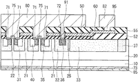
- FIG. 10 is a cross section schematically illustrating a structure in the vicinity of a gate pad in the semiconductor device in accordance with the preferred embodiment
- FIG. 11 is a cross section schematically illustrating a structure in the vicinity of an element peripheral portion in the semiconductor device in accordance with the preferred embodiment.
- FIG. 12 is a plan view schematically illustrating a structure of the semiconductor device in accordance with the preferred embodiment.
- FIG. 10 is a cross section schematically illustrating a structure in the vicinity of a gate pad in the semiconductor device in accordance with the present preferred embodiment.
- FIG. 11 is a cross section schematically illustrating a structure in the vicinity of an element peripheral portion in the semiconductor device in accordance with the present preferred embodiment.
- FIG. 12 is a plan view schematically illustrating a structure of the semiconductor device in accordance with the present preferred embodiment.
- FIG. 10 corresponds to an X-X′ cross section of FIG. 12 .
- FIG. 11 corresponds to a Y-Y′ cross section of FIG. 12 .
- the semiconductor device includes an n-type drift layer 20 formed on an upper surface of an n-type semiconductor substrate 10 . Further, the semiconductor device includes a back ohmic electrode 73 formed on a lower surface of the n-type semiconductor substrate 10 . Furthermore, the semiconductor device includes a drain electrode 85 formed on a lower surface of the back ohmic electrode 73 .
- well regions 31 are formed in a surface layer of the n-type drift layer 20 .
- a source region 40 and a high concentration well injection region 35 are formed.
- a gate insulating film 50 is formed across an upper surface of a separation region 21 which is a region between adjacent two of the plurality of well regions 31 . Further, a gate electrode 60 is formed on an upper surface of the gate insulating film 50 . Furthermore, an interlayer insulating film 55 is so formed as to cover the gate electrode 60 .
- a first Schottky electrode 75 is formed across an upper surface of another separation region 22 which is a region between other adjacent two of the plurality of well regions 31 . Further, a first ohmic electrode 71 is so formed as to sandwich the first Schottky electrode 75 in the cross sections exemplarily illustrated in FIGS. 10 and 11 . The first ohmic electrode 71 is formed across a surface layer of the source region 40 and a surface layer of the high concentration well injection region 35 .
- a source electrode 80 is so formed as to cover the interlayer insulating film 55 , the first ohmic electrode 71 , and the first Schottky electrode 75 .
- a well region 32 A is formed in the surface layer of the n-type drift layer 20 .
- a high concentration well injection region 36 is formed in a surface layer of the well region 32 A.
- a second ohmic electrode 72 is formed in a surface layer of the high concentration well injection region 36 .
- the source electrode 80 is so formed in a well contact hole 91 as to also cover the second ohmic electrode 72 .
- JTE junction termination extension
- a field insulating film 52 is formed across an upper surface of the well region 32 A and an upper surface of the JTE region 37 .
- the interlayer insulating film 55 is so formed as to also cover the field insulating film 52 .
- the gate pad 81 is formed on an upper surface of the interlayer insulating film 55 on the terminal region side.
- the well region 32 A is formed in the surface layer of the n-type drift layer 20 .
- the high concentration well injection region 36 is formed in a surface layer of the well region 32 A.
- the second ohmic electrode 72 is formed in the surface layer of the high concentration well injection region 36 .
- the source electrode 80 is so formed in the well contact hole 91 as to also cover the second ohmic electrode 72 .
- the JTE region 37 is formed.
- the field insulating film 52 is formed across the upper surface of the well region 32 A and the upper surface of the JTE region 37 .
- the interlayer insulating film 55 is so formed as to also cover the field insulating film 52 .
- the gate wire 82 is formed on the upper surface of the interlayer insulating film 55 on the terminal region side.
- the gate wire 82 covers the gate electrode 60 in a gate contact hole 95 .
- the first Schottky electrode 75 is formed in a portion below the source electrode 80 . Then, the first Schottky electrode 75 gets into contact with the separation region 22 formed by partially chipping the well region 31 . An SBD is thereby formed.
- the well region 32 A protruding toward the terminal region side of the source electrode 80 is formed.
- the well region 32 A forms a parasitic pn diode between the drift layer 20 and itself. Further, in a portion where the well region 32 A is formed, the first Schottky electrode 75 is not formed.
- an SBD current causes a voltage drop in the separation region 22 , the drift layer 20 , the semiconductor substrate 10 , or the like.
- a voltage exceeding the diffusion potential of the pn junction is generated between the source electrode 80 and the drain electrode 85 .
- the voltage of the source electrode 80 and that of the drain electrode 85 are applied to the pn diode formed of the well region 32 A and the drift layer 20 . Then, the forward current is carried in the pn diode.
- the stacking fault is extended and a breakdown voltage of the transistor is degraded. Specifically, when the transistor is off, a leakage current is generated and the element or the circuit is broken due to heat generation.
- an applied voltage between the source and the drain is limited to not higher than a constant value so that a bipolar current should not be carried in the pn diode formed of the well region 32 A and the drift layer 20 .
- reduced is the voltage generated between the source and the drain when a circulating current is carried. This case is accompanied with a disadvantage of increasing the cost due to an increase in the chip size.
- a method of increasing a contact resistance between the well region 32 A and the source electrode 80 may be used.
- another method of connecting the well region 32 A and the source electrode 80 with an external resistor may be used.
- the impurity concentration of the drift layer 20 is designed to be high since the drift layer 20 of low resistance is formed, taking an advantage of high dielectric breakdown electric field of the wide-gap semiconductor in the wide-gap semiconductor device, as compared with in a silicon semiconductor device.
- the impurity concentration of the drift layer 20 is designed to be high, consequently, a depletion capacitance between the source and the drain becomes significantly high. Then, when the switching is performed, a large displacement current is generated.
- the unipolar transistor incorporating the unipolar diode in its active region which is a semiconductor device using the wide-gap semiconductor
- there are two contradictory circumstances i.e., one is a circumstance requiring a decrease in the sheet resistance in the well region 32 A in order to increase the reliability of the element and the other is a circumstance requiring an increase in the sheet resistance.
- n-channel silicon carbide MOSFET which is a silicon carbide (SiC) semiconductor device, in which the first conductivity type is n type and the second conductivity type is p type, as one example of a semiconductor device.
- SiC silicon carbide
- the level (high or low) of a potential will be described, and in a case where it is assumed that the first conductivity type is p type and the second conductivity type is n type, the description on the level (high or low) of the potential is also a converse one.
- a region in which unit cells are periodically aligned is an active region and another region other than the active region is a terminal region.
- FIG. 1 is a cross section schematically illustrating a structure for realizing the semiconductor device in accordance with the present preferred embodiment.
- FIG. 2 is a plan view schematically illustrating a structure for realizing the semiconductor device in accordance with the present preferred embodiment.
- a drift layer 20 made of n-type (first conductivity type) silicon carbide As exemplarily illustrated in FIG. 1 , on a first main surface of a semiconductor substrate 10 made of n-type (first conductivity type) silicon carbide of low resistance, which has 4H polytype, formed is a drift layer 20 made of n-type (first conductivity type) silicon carbide.
- the first main surface is a (0001) plane in plane orientation and the first main surface is inclined by 4 degrees with respect to a c-axis direction.
- the drift layer 20 has a first impurity concentration of n type (first conductivity type).
- n type first conductivity type
- a drain electrode 85 is formed with a back ohmic electrode 73 interposed therebetween.
- the well region 31 has a second impurity concentration of p type (second conductivity type).
- the well region 31 is separated at two positions in a cross section inside the unit cell, and one is referred to as a separation region 21 and the other is referred to as a separation region 22 .
- the separation regions 21 and 22 are n-type (first conductivity type) regions in the surface layer of the drift layer 20 .
- the separation region 22 is formed, penetrating from a surface layer of the well region 31 in a depth direction.
- each well region 31 on a surface layer side inside each well region 31 , formed is an n-type (first conductivity type) source region 40 containing nitrogen (N) which is an n-type (first conductivity type) impurity.
- N nitrogen
- the depth in which the source region 40 is formed is shallower than the depth in which the well region 31 is formed.
- a gate electrode 60 is formed at a position in an upper surface of the gate insulating film 50 corresponding to the separation region 21 , the well region 31 , and an end portion of the source region 40 .
- the gate electrode 60 is formed on the upper surface of the well region 31 between the source region 40 and the drift layer 20 , with the gate insulating film 50 interposed therebetween.
- the region in the well region 31 which is sandwiched between the separation region 21 and the source region 40 and positioned below the gate electrode 60 with the gate insulating film 50 interposed therebetween is referred to as a channel region.
- the channel region is a region in which an inversion layer is formed when an on operation is performed.
- an interlayer insulating film 55 of silicon oxide is so formed as to cover the gate electrode 60 .
- a first ohmic electrode 71 for reducing a contact resistance with the silicon carbide.
- the well region 31 can easily give and receive electrons or positive holes to/from the first ohmic electrode 71 through the high concentration well injection region 35 of low resistance.
- a first Schottky electrode 75 On an upper surface of the separation region 22 , formed is a first Schottky electrode 75 .
- the first Schottky electrode 75 and the upper surface of the drift layer 20 corresponding to the separation region 22 are Schottky-connected to each other.
- the first Schottky electrode 75 should contain at least the upper surface of the separation region 22 , but the first Schottky electrode 75 may not contain the upper surface of the separation region 22 .
- a source electrode 80 On an upper surface of the first ohmic electrode 71 , an upper surface of the first Schottky electrode 75 , and an upper surface of the interlayer insulating film 55 , formed is a source electrode 80 .
- the source electrode 80 electrically short-circuits the first ohmic electrode 71 and the first Schottky electrode 75 .
- the first ohmic electrode 71 and the first Schottky electrode 75 are electrically connected to each other.
- a diffusion potential of an SBD formed by the contact of the first Schottky electrode 75 and the separation region 22 is lower than that of pn junction.
- the formation area of the well region 32 is larger than that of the well region 31 .
- n-type dividing region 25 is formed, being adjacent to the well region 32 from the terminal region side.
- An insulator is in contact with an upper surface of the dividing region 25 .
- a p-type well region 33 is formed, being adjacent to the n-type dividing region 25 from the terminal region side.
- the well region 33 is formed, sandwiching the well region 32 in a plan view.
- the formation area of the well region 33 is larger than that of the well region 32 .
- a field insulating film 52 having a film thickness larger than that of the gate insulating film 50 .
- the gate electrode 60 extends up to a position corresponding to above the well region 33 from the active region and is formed across the gate insulating film 50 on the upper surface of the well region 33 and the field insulating film 52 on the upper surface of the well region 33 .
- the gate electrode 60 and a gate wire 82 are in contact with each other with a gate contact hole 95 opened in the interlayer insulating film 55 .
- a gate pad 81 or the gate wire 82 is included in the well region 33 in a plan view. This is intended to prevent a high voltage from being applied to the field insulating film 52 below the gate wire 82 which is a wire having a potential which is significantly lower than a drain voltage because the well region 33 shields the high voltage to be applied to the drain electrode 85 .
- the gate electrode 60 is included in a region including all of the well region 31 , the well region 32 , the well region 33 , the separation region 21 , and the dividing region 25 in a plan view. It is thereby possible to prevent the high voltage from being applied to the gate insulating film 50 or the field insulating film 52 formed below the gate electrode 60 .
- the separation region 21 and the dividing region 25 are each n type, since a depletion layer extends into each of the n-type regions from the nearby well region, it is possible to prevent the high voltage from being applied to the gate insulating film 50 or the field insulating film 52 formed on the upper surfaces thereof.
- a p-type JTE region 37 having an impurity concentration lower than that of the well region 33 .
- the JTE region 37 is connected to the well region 33 .
- the well region 32 is connected to the source electrode 80 in a well contact hole 91 opened in the gate insulating film 50 and the interlayer insulating film 55 .
- the gate electrode 60 is partially removed in a portion in which the well contact hole 91 is formed.
- a second ohmic electrode 72 In a portion of the well contact hole 91 , in which the layer of silicon carbide and the source electrode 80 are in contact with each other, formed is a second ohmic electrode 72 .
- a high concentration well injection region 36 In the surface layer of the well region 32 which is in contact with the second ohmic electrode 72 , formed is a high concentration well injection region 36 .
- the high concentration well injection region 36 reduces a contact resistance between the second ohmic electrode 72 and the well region 32 , like the high concentration well injection region 35 .
- the well region 33 is not ohmic-connected to the source electrode 80 directly or even through the high concentration well injection region of the same p type.
- the dividing region 25 has an upper surface in contact with the gate insulating film 50 and a lower surface connected to the n-type drift layer 20 . For this reason, there is no conducting path through a p type or a conductor from the well region 32 toward the well region 33 . In other words, there is no conductive path serving as ohmic from the well region 33 to the source electrode 80 .
- the electrical conduction between the well region 33 and the source electrode 80 is performed through the dividing region 25 .
- the well region 32 , the dividing region 25 , and the well region 33 form a contact structure of pnp in a plane direction. Since there is reverse bias of the pn junction inside an energization path in any voltage direction, it is generally recognized that no current is carried. Actually, however, in a case where the width of the dividing region 25 is reduced, energization can be performed by applying a predetermined voltage.
- punch through occurs, in which a band barrier for majority carrier formed in an junction interface B disappears and energization is caused when a depletion layer extending from a junction interface A between the dividing region 25 and either one of the well regions toward the inside of the dividing region 25 reaches the junction interface B between the dividing region 25 and the other well region. Therefore, shown is the characteristic that until a punch through voltage is applied, almost no current is carried but when a voltage exceeding the punch through voltage is applied, currents abruptly flow.
- the punch through voltage is derived as follows:
- V qNW 2 ( 2 ⁇ ⁇ ) ( 2 )
- q represents an elementary electric charge
- N represents an effective impurity concentration of the dividing region 25
- W represents a width of the dividing region 25
- ⁇ represents a dielectric constant of the semiconductor.
- the width of the dividing region 25 refers to the width in a direction connecting the well region 32 and the well region 33 and the width in the left and right direction of FIG. 1 .
- the punch through voltage in this case can be derived by giving the lowest impurity concentration within a range of a region in the dividing region 25 between the well region 32 and the well region 33 , having the depth shallower than that of at least one of the well region 32 and the well region 33 , as “N” in Eq. (2). This is because the punch through occurs earliest at a portion having the lowest impurity concentration.
- the reason why the dividing region 25 is brought into contact with the gate insulating film 50 is because in a case where a conductive structure is formed on the upper surface of the dividing region 25 , there is a possibility that a current path which goes around the dividing region 25 and has a short distance and a low resistance may be formed.
- the gate insulating film 50 is taken as an example of the structure formed on the upper surface of the dividing region 25 in the structure of the present preferred embodiment, the field insulating film 52 or the interlayer insulating film 55 may be formed thereon, and any other material may be used only if the structure is a nonconductor.
- the MOSFET incorporating the SBD in accordance with the present preferred embodiment will be described.
- silicon carbide is taken.
- the diffusion potential of the pn junction is substantially 2 V.
- the dividing region 25 is interposed in the current path between the source and the drain, most of the voltage between the source and the drain is applied to the dividing region 25 and it is thereby possible to reduce the voltage to be applied to the pn junction.
- the voltage to be applied to the pn junction to be lower than 2 V which corresponds to the diffusion potential of the pn junction, it is possible to suppress the forward current from being carried in the pn diode.
- the dividing region 25 can cut off the voltage of several V equivalent to the voltage obtained by subtracting the diffusion potential of the pn junction from the generated voltage between the source and the drain, the above-described effect can be produced.
- the generated voltage between the source and the drain is 5 V
- the punch through voltage of the dividing region 25 it is possible to make the forward voltage applied to the pn junction not higher than 2 V at a position farther than the dividing region 25 and prevent forward energization of the pn diode in this region.
- the punch through voltage of the dividing region 25 is lower than 3 V, it is possible to reduce the voltage to be applied to the pn junction and produce an effect of reducing the forward current in the pn diode and reducing the probability of occurrence of breakdown, to some degree.
- the gate electrode 60 , the gate pad 81 , and the gate wire 82 need to be included in a planar region including the well region 31 , the well region 32 , the well region 33 , the separation region 21 , and the dividing region 25 in a plan view.
- the gate electrode 60 , the gate pad 81 , and the gate wire 82 need to be included in at least one of the well region 32 and the well region 33 .
- the region in which the well region 32 and the well region 33 are formed needs to include the gate pad 81 wide enough to form a wire bond, a region for forming a contact between the gate pad 81 or the gate wire 82 and the gate electrode 60 , and the like. This requires a wide area.
- the forming position of the dividing region 25 should be closer to the well contact hole 91 and the area of the well region 32 should be as small as possible, instead of increasing the area of the well region 33 .
- the regions in which it is possible to suppress the forward voltage exceeding the diffusion potential from being applied to the pn junction thereby increase, and it is possible to prevent the forward energization in the pn diode in most regions. Therefore, a semiconductor device with its reliability significantly increased can be obtained. From the above description, it is desirable that the area of the well region 32 should be smaller than that of the well region 33 .
- the above holes go from a pn junction surface formed between the well region 32 and the well region 33 , and the drift layer 20 toward the source electrode 80 , and the displacement current is thereby carried in the chip plane direction.
- the displacement current generated from the well region 33 goes through the dividing region 25 .
- the generated voltage of the well region 33 increases by a voltage which corresponds to the punch through voltage of the dividing region 25 .
- the punch through voltage of the dividing region 25 obtained from Eq. (2) it is necessary to design the punch through voltage of the dividing region 25 obtained from Eq. (2) to be lower than a dielectric breakdown voltage of the gate insulating film 50 between the well region 33 and the gate pad 81 serving as a gate potential, between the well region 33 and the gate wire 82 , or between the well region 33 and the gate electrode 60 .
- the gate insulating film 50 of the MOSFET using silicon carbide generally, silicon oxide having a thickness of about 50 nm is used. In this case, since the dielectric breakdown electric field of silicon oxide is about 10 MV/cm, the withstand voltage is about 50 V.
- V in Eq. (2) it is necessary to set V in Eq. (2) to be not higher than 50 V.
- V in Eq. (2) when a high electric field exceeding half of the dielectric breakdown electric field is applied to an insulating film, considering the possibility of degradation of the reliability, it is further desirable to set V in Eq. (2) to be not hither than half of the dielectric breakdown voltage of the gate insulating film 50 , i.e., not higher than 25 V.
- the punch through voltage thereof is higher than a value obtained by subtracting the diffusion potential of the pn junction from the generated voltage between the source and the drain during the reflux operation and to be lower than the breakdown voltage of the gate insulating film 50 formed on the upper surface of the well region 33 (more desirably, to be not higher than half of the breakdown voltage of the gate insulating film 50 ), it is possible to suppress the breakdown of the gate insulating film 50 during the switching operation while suppressing the energization of the pn diode during the reflux operation in the well region 33 .
- CVD chemical vapor deposition
- an implantation mask is formed of a photoresist or the like, and Al which is a p-type impurity is ion-implanted.
- the depth of the ion implantation of Al does not exceed the thickness of the drift layer 20 and is, for example, not smaller than 0.5 ⁇ m and not larger than 3 ⁇ m.
- the impurity concentration of Al which is ion-implanted is, for example, in a range of not lower than 1 ⁇ 10 17 cm ⁇ 3 and not higher than 1 ⁇ 10 19 cm ⁇ 3 , which is higher than the first impurity concentration of the drift layer 20 .
- the implantation mask is removed.
- the region into which Al is ion-implanted in this process step becomes the well region 31 .
- This process step may be a process step performed at the same time as the process step for forming the well region 31 . In that case, the number of process steps can be reduced.
- the dividing region 25 is formed as a remaining portion in which the well region 32 and the well region 33 are not formed.
- the impurity concentration of the first conductivity type of the dividing region 25 is equivalent to the impurity concentration of the drift layer 20 .
- the impurity concentration of the dividing region 25 may be adjusted to a desired one different from that of the drift layer 20 .
- the width of the dividing region 25 required to realize the same punch through voltage can be reduced and reduction in the chip size and improvement of the breakdown voltage are expected.
- the implantation mask is formed of the photoresist or the like. Then, ion implantation of Al which is a p-type impurity is performed from above the implantation mask.
- the depth of the ion implantation of Al does not exceed the thickness of the drift layer 20 and is, for example, not smaller than 0.5 ⁇ m and not larger than 3 ⁇ m.
- the impurity concentration of Al which is ion-implanted is, for example, in a range of not lower than 1 ⁇ 10 16 cm ⁇ 3 and not higher than 1 ⁇ 10 18 cm ⁇ 3 , which is higher than the first impurity concentration of the drift layer 20 and lower than the Al concentration of the well region 31 .
- the region into which Al is ion-implanted in this process step becomes the JTE region 37 .
- the implantation mask is formed of the photoresist or the like, and N (nitrogen) which is an n-type impurity is ion-implanted.
- the depth of the ion implantation of N is shallower than the thickness of the well region 31 .
- the impurity concentration of N which is ion-implanted is, for example, in a range of not lower than 1 ⁇ 10 18 cm ⁇ 3 and not higher than 1 ⁇ 10 21 cm ⁇ 3 and exceeds the second impurity concentration of p type of the well region 31 .
- a region of n type becomes the source region 40 .
- the implantation mask is formed of the photoresist or the like, and Al which is a p-type impurity is ion-implanted. Then, the implantation mask is removed. The region into which Al is implanted in this process step becomes the high concentration well injection region 35 .
- the high concentration well injection region 35 is a region provided to achieve an excellent electrical contact between the well region 31 and the first ohmic electrode 71 , and it is desirable that the p-type impurity concentration of the high concentration well injection region 35 should be set higher than the second impurity concentration of p type of the well region 31 .
- the ion implantation should be performed after heating the semiconductor substrate 10 or the drift layer 20 to 150° C. or higher.
- the high concentration well injection region 36 is formed.
- the number of process steps for the formation may be reduced.
- the process cost can become lower and the chip cost can be reduced.
- annealing is performed by using a heat treatment apparatus, for example, at a temperature not lower than 1300° C. and not higher than 1900° C. for not shorter than 30 seconds and not longer than one hour.
- a heat treatment apparatus for example, at a temperature not lower than 1300° C. and not higher than 1900° C. for not shorter than 30 seconds and not longer than one hour.
- the field insulating film 52 at the position almost corresponding to a cell region should be removed by the photolithography technique, etching, or the like.
- the upper surface of the silicon carbide not covered with the field insulating film 52 is thermally oxidized and the silicon oxide which is the gate insulating film 50 , having a desired thickness, is thereby formed.
- a polycrystalline silicon film having conductivity is formed by the low-pressure CVD method. Then, by patterning the polycrystalline silicon film, the gate electrode 60 is formed.
- the interlayer insulating film 55 is formed by the low-pressure CVD method. Then, a contact hole which penetrates the interlayer insulating film 55 and the gate insulating film 50 and reaches the high concentration well injection region 35 and the source region 40 in the unit cell is formed and the well contact hole 91 is formed at the same time.
- a heat treatment is performed, for example, at a temperature not lower than 600° C. and not higher than 1100° C. Then, by reacting the metal film made mainly of Ni with a silicon carbide layer inside the contact hole, silicide is formed between the silicon carbide layer and the metal film.
- the metal film remaining on the interlayer insulating film 55 other than the silicide formed by the above-described reaction, is removed by wet etching.
- the first ohmic electrode 71 is thereby formed.
- the back ohmic electrode 73 is formed on the back side of the semiconductor substrate 10 .
- the interlayer insulating film 55 on the upper surface of the separation region 22 , the interlayer insulating film 55 formed at the position to become the gate insulating film 50 , and the interlayer insulating film 55 formed at the position to become the gate contact hole 95 are removed.
- a removing method it is preferable to use wet etching which produces no damage on the upper surface of the silicon carbide which is to become an SBD interface.
- the first Schottky electrode 75 is deposited.
- the first Schottky electrode 75 it is preferable to deposit, for example, titanium (Ti), molybdenum (Mo), Ni, or the like.
- a wiring metal of Al or the like is formed on the upper surface of the semiconductor substrate 10 having been subjected to these treatments. Then, by processing the wiring metal into a predetermined shape with the photolithography technique, the source electrode 80 in contact with the first ohmic electrode 71 and the first Schottky electrode 75 , and the gate wire 82 in contact with the gate electrode 60 are formed.
- the drain electrode 85 which is a metal film is formed.
- FIG. 3 is a cross section schematically illustrating a structure for realizing a semiconductor device in accordance with the present preferred embodiment.
- the active region having the well region 31 is clearly distinguished from the well region 32 in the first preferred embodiment, there may be a case where no well region 32 is present and the dividing region 25 is formed between the well region 31 on the outermost side (terminal region side) among the well regions 31 and the well region 33 , as exemplarily illustrated in FIG. 3 .
- the dividing region 25 formed between the well region 31 and the well region 33 performs the same function as that of the dividing region 25 formed between the well region 31 and the well region 32 .
- the description in the first preferred embodiment can be understood by interpreting the well region 31 on the outermost side as the second well.
- FIG. 4 is a cross section schematically illustrating a structure for realizing a semiconductor device in accordance with the present preferred embodiment.
- FIG. 5 is a plan view schematically illustrating a structure for realizing the semiconductor device in accordance with the present preferred embodiment.
- a dividing region 25 B around a well region 32 B is so formed as to surround the well region 32 B, the second ohmic electrode 72 , and the well contact hole 91 in a plan view.
- a method of manufacturing the semiconductor device of the present preferred embodiment is almost the same as that in the case exemplarily illustrated in the first preferred embodiment, and it is only necessary to simply change a mask pattern for forming the well region 32 B and a well region 33 B.
- FIG. 6 is a cross section schematically illustrating a structure for realizing a semiconductor device in accordance with the present preferred embodiment.
- an SBD region is formed inside the region in which the well contact hole 91 is formed.
- an n-type separation region 23 obtained by partially chipping a well region 32 C is formed.
- the separation region 23 is formed, penetrating from a surface layer of the well region 32 C in the depth direction.
- a second Schottky electrode 76 is formed on an upper surface of the separation region 23 .
- the second ohmic electrode 72 and a high concentration well injection region 36 C are also chipped.
- the SBD current can be carried also below the well region 32 C.
- a voltage drop occurs in the drift layer 20 below the well region 32 C or the semiconductor substrate 10 , and the forward voltage to be applied to the pn junction formed between the well region 32 C and the drift layer 20 is reduced by the dropped voltage.
- the energization of the pn diode in the well region 32 C is suppressed and it is possible to obtain the semiconductor device with higher reliability.
- a method of manufacturing the semiconductor device of the present preferred embodiment is almost the same as that in the case exemplarily illustrated in the first preferred embodiment, and it is only necessary to simply change a mask pattern for forming the well region 32 C, the well region 33 , and the high concentration well injection region 36 C and then form the second Schottky electrode 76 by the same method as that of forming the first Schottky electrode 75 .
- FIG. 7 is a cross section schematically illustrating a structure for realizing a semiconductor device in accordance with the present preferred embodiment.
- a field insulating film 52 D is formed in the entire region in which the well region 33 and the gate electrode 60 overlap each other in a plan view. Particularly in FIG. 7 , the field insulating film 52 D is so formed as to cover the entire upper surface of the well region 33 .
- no gate insulating film 50 D is formed in the entire region in which the well region 33 and the gate electrode 60 overlap each other in a plan view. In other words, it can be expressed that a boundary between the gate insulating film 50 D and the field insulating film 52 D is positioned on an upper surface of a well region 32 D.
- the gate insulating film 50 is broken and an element failure thereby occurs.
- no gate insulating film is formed on the upper surface of the well region 33 , and the field insulating film 52 D having an overwhelmingly high dielectric breakdown voltage is formed instead.
- FIG. 8 is a cross section schematically illustrating a structure for realizing a semiconductor device in accordance with the present preferred embodiment.
- a p-type high concentration well injection region 38 is formed over a relatively wide range in a surface layer of a well region 33 E.
- the impurity concentration of the high concentration well injection region 38 is higher than that of the well region 31 .
- an implantation step in which the high concentration well injection region 38 is formed has only to be added to the method exemplarily illustrated in the first preferred embodiment.
- the implantation for the high concentration well injection region 38 is performed at the same time as the implantation for the high concentration well injection region 35 or the implantation for the high concentration well injection region 36 , it is possible to obtain the structure of the semiconductor device in accordance with the present preferred embodiment without increasing the number of process steps.
- FIG. 9 is a plan view schematically illustrating a structure for realizing a semiconductor device in accordance with the present preferred embodiment.
- a p-type auxiliary conductive region 34 is formed in, for example, part of a surface layer of a dividing region 25 F.
- a plurality of auxiliary conductive regions 34 are formed. With each of the auxiliary conductive regions 34 , the well region 32 and the well region 33 are electrically connected to each other.
- the potential of the well region 33 is not brought into a floating state, and it is possible to suppress problems such as a change in the withstand voltage characteristics due to charge-up, or the like.
- the total length in which the auxiliary conductive region 34 is formed in the chip should be shorter than the total length in which the dividing region 25 F is formed.
- the term “length” in the description on the length in which the auxiliary conductive region 34 is formed and the length in which the dividing region 25 F is formed refers to a length in a direction intersecting the direction connecting the well region 32 and the well region 33 .
- the auxiliary conductive region 34 is formed to be not larger than one tenth of the total length in which the dividing region 25 F is formed, the possibility of causing the breakdown voltage degradation is reduced to not larger than about one tenth and it is possible to significantly increase the reliability of the element.
- a method of manufacturing the semiconductor device of the present preferred embodiment is almost the same as that in the case exemplarily illustrated in the first preferred embodiment, and an implantation step in which the auxiliary conductive region 34 is formed has only to be added. Alternatively, it is only necessary to change a mask pattern so that the implantation for any one of the JTE region 37 , the well region 31 , the well region 32 , and the well region 33 and the implantation for the auxiliary conductive region 34 may be performed at the same time.
- the semiconductor device includes a drift layer 20 of a first conductivity type, a first well region of a second conductivity type, a first separation region of the first conductivity type, a source region 40 of the first conductivity type, a first Schottky electrode 75 , a first ohmic electrode 71 , a second well region of the second conductivity type, a third well region of the second conductivity type, a second ohmic electrode 72 , a dividing region 25 of the first conductivity type, and a source electrode 80 .
- the well region 31 corresponds to the first well region.
- the separation region 22 corresponds to the first separation region.
- the well region 32 corresponds to the second well region.
- the drift layer 20 is a wide-gap semiconductor layer provided on an upper surface of a semiconductor substrate 10 of the first conductivity type.
- a plurality of well regions 31 are provided, being separated from one another in a surface layer of the drift layer 20 .
- the separation region 22 is provided penetrating from a surface layer of each of the well regions 31 in a depth direction.
- the source region 40 is provided in the surface layer of each of the well regions 31 .
- the first Schottky electrode 75 is provided on an upper surface of the separation region 22 .
- the first ohmic electrode 71 is provided at least partially in a surface layer of the source region 40 .
- the well region 32 is so provided in the surface layer of the drift layer 20 as to sandwich the whole of the plurality of well regions 31 in a plan view and has an area larger than that of each of the well regions 31 .
- the well region 33 is so provided in the surface layer of the drift layer 20 as to sandwich the well region 32 in a plan view and has an area larger than that of the well region 32 .
- the second ohmic electrode 72 is provided in part of the well region 32 .
- the dividing region 25 is provided between the well region 32 and the well region 33 , having an upper surface which is in contact with an insulator.
- the source electrode 80 is connected to the first Schottky electrode 75 , the first ohmic electrode 71 , and the second ohmic electrode 72 .
- the dividing region 25 cuts off the current and it is thereby possible to significantly narrow the region in which the forward current is carried in the pn diode. Therefore, it is possible to significantly suppress the possibility of causing the degradation of the breakdown voltage due to extension of the stacking fault.
- the current is carried in the dividing region 25 , and it is thereby possible to suppress the element destruction. Therefore, it is possible to significantly increase the reliability of the semiconductor device. Further, by maintaining high-speed switching, it is possible to reduce the switching loss. Moreover, it is possible to increase the circulating current to be energized. Further, since the chip size can be reduced, it is possible to achieve low cost.
- the semiconductor device includes a gate electrode 60 .
- the gate electrode 60 is provided on an upper surface of the well region 31 sandwiched between the source region 40 and the drift layer 20 , with a gate insulating film 50 interposed therebetween. Furthermore, the gate electrode 60 is provided also in a region corresponding to an upper surface of the well region 33 . With such a structure, it is possible to effectively suppress the forward voltage shift due to occurrence of the stacking fault.
- the well region 33 has no ohmic connection to the source electrode 80 .
- the electrical conduction between the well region 33 and the source electrode 80 is performed through the dividing region 25 .
- the voltage applied to the pn junction is a voltage lower than 2 V which corresponds to the diffusion potential of the pn junction, it is possible to suppress the forward current from flowing in the pn diode.
- a voltage V obtained from the following Eq. 3 is not higher than 50 V
- V qNW 2 ( 2 ⁇ ⁇ ) ( 3 ) where the width of the dividing region 25 in a direction connecting the well region 32 and the well region 33 is W, the effective impurity concentration of the dividing region 25 is N, the dielectric constant of the semiconductor is E, and the elementary electric charge is q.
- the dividing region 25 between the well region 32 and the well region 33 by forming the dividing region 25 between the well region 32 and the well region 33 and designing the punch through voltage thereof to be higher than a value obtained by subtracting the diffusion potential of the pn junction from the generated voltage between the source and the drain during the reflux operation and to be lower than the breakdown voltage of the gate insulating film 50 formed on the upper surface of the well region 33 , it is possible to suppress the breakdown of the gate insulating film 50 during the switching operation while suppressing the energization of the pn diode during the reflux operation in the well region 33 .
- a dividing region 25 B surrounds the second ohmic electrode 72 in a plan view.
- the semiconductor device includes a second separation region of the first conductivity type and a second Schottky electrode 76 .
- the separation region 23 corresponds to the second separation region.
- the separation region 23 is provided penetrating from a surface layer of a well region 32 C in a depth direction.
- the second Schottky electrode 76 is provided on an upper surface of the separation region 23 .
- the semiconductor device includes a field insulating film 52 provided in at least part of the upper surface of the well region 33 .
- the thickness of the field insulating film 52 is larger than that of the gate insulating film 50 .
- the gate electrode 60 is provided on the upper surface of the well region 33 , with the field insulating film 52 interposed therebetween, in a region in which the field insulating film 52 is provided. With such a structure, it is possible to suppress the breakdown due to the displacement current during the switching operation.
- the gate electrode 60 is provided on the upper surface of the well region 33 , with a field insulating film 52 D interposed therebetween, in the region corresponding to the upper surface of the well region 33 .
- the semiconductor device includes a well injection region of the second conductivity type.
- the high concentration well injection region 38 corresponds to the well injection region.
- the high concentration well injection region 38 is provided in a surface layer of a well region 33 E.
- the impurity concentration of the high concentration well injection region 38 is higher than that of the well region 31 .
- the semiconductor device includes at least one auxiliary conductive region 34 of the second conductivity type.
- the auxiliary conductive region 34 is provided in a surface layer of a dividing region 25 F. Further, the auxiliary conductive region 34 electrically connects the well region 32 and the well region 33 . With such a structure, the potential of the well region 33 is not brought into a floating state, and it is possible to suppress problems such as a change in the withstand voltage characteristics due to charge-up, or the like.
- a total length in which the auxiliary conductive region 34 is provided is not larger than one tenth of a total length in which the dividing region 25 F is provided.
- the length in which the auxiliary conductive region 34 is provided is a length in which the auxiliary conductive region 34 is provided in a direction intersecting a direction connecting the well region 32 and the well region 33 .
- the length in which the dividing region 25 F is provided is a length in which the dividing region 25 F is provided in a direction intersecting a direction connecting the well region 32 and the well region 33 .
- the potential of the well region 33 is not brought into a floating state, and it is possible to suppress problems such as a change in the withstand voltage characteristics due to charge-up, or the like. Further, the possibility of causing the breakdown voltage degradation can be reduced to not larger than about one tenth, and it is possible to significantly increase the reliability of the element.
- the unipolar transistor incorporating the unipolar diode the MOSFET incorporating the SBD has been exemplarily illustrated.
- the above-described techniques can be also applied to any other unipolar device.
- the unipolar transistor may be a junction field effect transistor (JFET), instead of the MOSFET.
- JFET junction field effect transistor
- FET field effect transistor
- the present invention can be applied to any other wide-gap semiconductor.
- the wide-gap semiconductor generally refers to a semiconductor having a band gap of about 2 eV or higher, and well known are a group III nitride such as gallium nitride (GaN) or the like, a group II oxide such as zinc oxide (ZnO) or the like, a group II chalcogenide such as zinc selenide (ZnSe) or the like, diamond, silicon carbide, and the like.
- a group III nitride such as gallium nitride (GaN) or the like
- a group II oxide such as zinc oxide (ZnO) or the like
- ZnSe zinc selenide
- each constituent element in the above-described preferred embodiments is a conceptual unit, including cases where one constituent element is constituted of a plurality of structures, where one constituent element corresponds to part of a structure, and where a plurality of constituent elements are included in one structure, within the scope of the technique disclosed in the specification of the present application.
- each constituent element in the above-described preferred embodiments includes a structure having any other constitution or shape, as long as the same function can be performed.
- the material includes the same containing any other additive, such as an alloy, as long as no contradiction arises.
- planar MOSFET has been described in the above-described preferred embodiments, a case where the present invention is applied to a trench MOSFET in which a trench is formed on the upper surface of the drift layer 20 can be also assumed.
- a trench is formed on the upper surface of the drift layer 20 and the gate electrode is buried on the upper surface of the drift layer 20 in the trench, i.e., a bottom surface of the trench with the gate insulating film interposed therebetween.
Abstract
Description
from the above one-dimensional Poisson's equation, as the solution of x=W;
where the width of the dividing
Claims (12)
Applications Claiming Priority (1)
| Application Number | Priority Date | Filing Date | Title |
|---|---|---|---|
| PCT/JP2016/061706 WO2017179102A1 (en) | 2016-04-11 | 2016-04-11 | Semiconductor device |
Publications (2)
| Publication Number | Publication Date |
|---|---|
| US20190181259A1 US20190181259A1 (en) | 2019-06-13 |
| US11222973B2 true US11222973B2 (en) | 2022-01-11 |
Family
ID=60042498
Family Applications (1)
| Application Number | Title | Priority Date | Filing Date |
|---|---|---|---|
| US16/082,212 Active US11222973B2 (en) | 2016-04-11 | 2016-04-11 | Semiconductor device |
Country Status (5)
| Country | Link |
|---|---|
| US (1) | US11222973B2 (en) |
| JP (1) | JP6560444B2 (en) |
| CN (1) | CN108886038B (en) |
| DE (1) | DE112016006723T5 (en) |
| WO (1) | WO2017179102A1 (en) |
Families Citing this family (8)
| Publication number | Priority date | Publication date | Assignee | Title |
|---|---|---|---|---|
| JP6293380B1 (en) | 2016-04-21 | 2018-03-14 | 三菱電機株式会社 | Semiconductor device |
| DE112017004237B4 (en) * | 2016-08-25 | 2023-12-14 | Mitsubishi Electric Corporation | SEMICONDUCTOR UNIT |
| JP6678810B2 (en) * | 2017-02-24 | 2020-04-08 | 三菱電機株式会社 | Silicon carbide semiconductor device and power converter |
| JP6873273B2 (en) | 2017-12-19 | 2021-05-19 | 三菱電機株式会社 | Silicon carbide semiconductor device and power conversion device |
| US11049963B2 (en) | 2017-12-19 | 2021-06-29 | Mitsubishi Electric Corporation | Silicon carbide semiconductor device and power converter |
| US11355627B2 (en) | 2017-12-19 | 2022-06-07 | Mitsubishi Electric Corporation | Silicon carbide semiconductor device and power converter |
| US20220254906A1 (en) * | 2019-09-06 | 2022-08-11 | Mitsubishi Electric Corporation | Silicon carbide semiconductor device and power converter |
| US20230142729A1 (en) * | 2021-11-08 | 2023-05-11 | Analog Devices, Inc. | Integrated device package with an integrated heat sink |
Citations (11)
| Publication number | Priority date | Publication date | Assignee | Title |
|---|---|---|---|---|
| JPH04229661A (en) | 1990-06-08 | 1992-08-19 | Nippondenso Co Ltd | Insulated-gate bipolar transistor and its manufacture |
| JP2001094095A (en) | 1999-09-21 | 2001-04-06 | Denso Corp | Silicon carbide semiconductor device and fabrication method thereof |
| JP2003017701A (en) | 2001-07-04 | 2003-01-17 | Denso Corp | Semiconductor device |
| JP2004289023A (en) | 2003-03-24 | 2004-10-14 | Fuji Electric Advanced Technology Co Ltd | Inspecting method and apparatus for silicon carbide semiconductor device, and manufacturing method for silicon carbide semiconductor device |
| US20130168700A1 (en) * | 2010-06-24 | 2013-07-04 | Mitsubishi Electric Corporation | Power semiconductor device |
| US8492836B2 (en) * | 2009-10-14 | 2013-07-23 | Mitsubishi Electric Corporation | Power semiconductor device |
| US8513735B2 (en) * | 2008-12-25 | 2013-08-20 | Mitsubishi Electric Corporation | Power semiconductor device |
| WO2014038110A1 (en) | 2012-09-06 | 2014-03-13 | 三菱電機株式会社 | Semiconductor device |
| WO2014162969A1 (en) | 2013-04-03 | 2014-10-09 | 三菱電機株式会社 | Semiconductor device |
| US20150340443A1 (en) * | 2014-05-21 | 2015-11-26 | Sumitomo Electric Industries, Ltd. | Silicon carbide semiconductor device |
| US20180097103A1 (en) * | 2015-04-22 | 2018-04-05 | Mitsubishi Electric Corporation | Semiconductor device and semiconductor device manufacturing method |
Family Cites Families (8)
| Publication number | Priority date | Publication date | Assignee | Title |
|---|---|---|---|---|
| JP3850580B2 (en) * | 1999-03-30 | 2006-11-29 | 株式会社東芝 | Semiconductor device |
| JP5011612B2 (en) * | 2000-10-31 | 2012-08-29 | 富士電機株式会社 | Semiconductor device |
| JP4585772B2 (en) * | 2004-02-06 | 2010-11-24 | 関西電力株式会社 | High breakdown voltage wide gap semiconductor device and power device |
| WO2012001837A1 (en) * | 2010-06-30 | 2012-01-05 | 三菱電機株式会社 | Power semiconductor device |
| JP5159987B1 (en) | 2011-10-03 | 2013-03-13 | パナソニック株式会社 | Semiconductor device, power converter, and control method of power converter |
| JP6072432B2 (en) * | 2012-05-15 | 2017-02-01 | 三菱電機株式会社 | Semiconductor device and manufacturing method thereof |
| JP5939448B2 (en) * | 2013-04-30 | 2016-06-22 | 日産自動車株式会社 | Semiconductor device and manufacturing method thereof |
| JP6244762B2 (en) * | 2013-09-12 | 2017-12-13 | 住友電気工業株式会社 | Silicon carbide semiconductor device |
-
2016
- 2016-04-11 JP JP2018511559A patent/JP6560444B2/en active Active
- 2016-04-11 WO PCT/JP2016/061706 patent/WO2017179102A1/en active Application Filing
- 2016-04-11 US US16/082,212 patent/US11222973B2/en active Active
- 2016-04-11 DE DE112016006723.2T patent/DE112016006723T5/en active Pending
- 2016-04-11 CN CN201680084166.3A patent/CN108886038B/en active Active
Patent Citations (15)
| Publication number | Priority date | Publication date | Assignee | Title |
|---|---|---|---|---|
| US5169793A (en) | 1990-06-08 | 1992-12-08 | Nippondenso Co., Ltd. | Method of making an insulated gate bipolar transistor having gate shield region |
| US5464992A (en) | 1990-06-08 | 1995-11-07 | Nippondenso Co., Ltd. | Insulated gate bipolar transistor provided with a minority carrier extracting layer |
| JPH04229661A (en) | 1990-06-08 | 1992-08-19 | Nippondenso Co Ltd | Insulated-gate bipolar transistor and its manufacture |
| JP2001094095A (en) | 1999-09-21 | 2001-04-06 | Denso Corp | Silicon carbide semiconductor device and fabrication method thereof |
| JP2003017701A (en) | 2001-07-04 | 2003-01-17 | Denso Corp | Semiconductor device |
| JP2004289023A (en) | 2003-03-24 | 2004-10-14 | Fuji Electric Advanced Technology Co Ltd | Inspecting method and apparatus for silicon carbide semiconductor device, and manufacturing method for silicon carbide semiconductor device |
| US8513735B2 (en) * | 2008-12-25 | 2013-08-20 | Mitsubishi Electric Corporation | Power semiconductor device |
| US8492836B2 (en) * | 2009-10-14 | 2013-07-23 | Mitsubishi Electric Corporation | Power semiconductor device |
| US20130168700A1 (en) * | 2010-06-24 | 2013-07-04 | Mitsubishi Electric Corporation | Power semiconductor device |
| WO2014038110A1 (en) | 2012-09-06 | 2014-03-13 | 三菱電機株式会社 | Semiconductor device |
| US20150236012A1 (en) | 2012-09-06 | 2015-08-20 | Mitsubishi Electric Corporation | Semiconductor device |
| WO2014162969A1 (en) | 2013-04-03 | 2014-10-09 | 三菱電機株式会社 | Semiconductor device |
| US20160079411A1 (en) * | 2013-04-03 | 2016-03-17 | Mitsubishi Electric Corporation | Semiconductor device |
| US20150340443A1 (en) * | 2014-05-21 | 2015-11-26 | Sumitomo Electric Industries, Ltd. | Silicon carbide semiconductor device |
| US20180097103A1 (en) * | 2015-04-22 | 2018-04-05 | Mitsubishi Electric Corporation | Semiconductor device and semiconductor device manufacturing method |
Non-Patent Citations (1)
| Title |
|---|
| International Search Report dated May 17, 2016 in PCT/JP2016/061706 filed Apr. 11, 2016. |
Also Published As
| Publication number | Publication date |
|---|---|
| JP6560444B2 (en) | 2019-08-14 |
| DE112016006723T5 (en) | 2018-12-20 |
| CN108886038B (en) | 2023-05-02 |
| WO2017179102A1 (en) | 2017-10-19 |
| JPWO2017179102A1 (en) | 2018-08-30 |
| US20190181259A1 (en) | 2019-06-13 |
| CN108886038A (en) | 2018-11-23 |
Similar Documents
| Publication | Publication Date | Title |
|---|---|---|
| US11222973B2 (en) | Semiconductor device | |
| EP1503425B1 (en) | Heterojunction semiconductor device and method of manufacturing the same | |
| US7700971B2 (en) | Insulated gate silicon carbide semiconductor device | |
| US7781786B2 (en) | Semiconductor device having a heterojunction diode and manufacturing method thereof | |
| US10128370B2 (en) | Semiconductor device | |
| EP1204145B1 (en) | Semiconductor element | |
| US11081598B2 (en) | Trench MOS Schottky diode | |
| JP6649183B2 (en) | Semiconductor device | |
| CN109564942B (en) | Semiconductor device with a plurality of semiconductor chips | |
| US10770581B2 (en) | Semiconductor device | |
| JP7176239B2 (en) | semiconductor equipment | |
| US20150279983A1 (en) | Semiconductor device | |
| US10147813B2 (en) | Tunneling field effect transistor | |
| US11888057B2 (en) | Semiconductor device | |
| US10714571B2 (en) | Silicon carbide semiconductor device having halogen field limiting ring regions and method of manufacturing same | |
| US20230017518A1 (en) | Semiconductor device | |
| US11908929B2 (en) | Semiconductor device | |
| JP7196265B2 (en) | semiconductor equipment | |
| JP6752336B2 (en) | Semiconductor device | |
| US20220246729A1 (en) | Silicon carbide vertical conduction mosfet device and manufacturing process thereof | |
| US20240145589A1 (en) | Semiconductor device | |
| US20220246723A1 (en) | Silicon carbide vertical conduction mosfet device for power applications and manufacturing process thereof | |
| JP2022120263A (en) | Silicon carbide semiconductor device | |
| JP2022159941A (en) | Semiconductor device |
Legal Events
| Date | Code | Title | Description |
|---|---|---|---|
| AS | Assignment |
Owner name: MITSUBISHI ELECTRIC CORPORATION, JAPAN Free format text: ASSIGNMENT OF ASSIGNORS INTEREST;ASSIGNORS:HINO, SHIRO;SADAMATSU, KOJI;HATTA, HIDEYUKI;AND OTHERS;SIGNING DATES FROM 20180723 TO 20180724;REEL/FRAME:047008/0278 |
|
| FEPP | Fee payment procedure |
Free format text: ENTITY STATUS SET TO UNDISCOUNTED (ORIGINAL EVENT CODE: BIG.); ENTITY STATUS OF PATENT OWNER: LARGE ENTITY |
|
| STPP | Information on status: patent application and granting procedure in general |
Free format text: NON FINAL ACTION MAILED |
|
| STPP | Information on status: patent application and granting procedure in general |
Free format text: RESPONSE TO NON-FINAL OFFICE ACTION ENTERED AND FORWARDED TO EXAMINER |
|
| STPP | Information on status: patent application and granting procedure in general |
Free format text: FINAL REJECTION MAILED |
|
| STPP | Information on status: patent application and granting procedure in general |
Free format text: RESPONSE AFTER FINAL ACTION FORWARDED TO EXAMINER |
|
| STPP | Information on status: patent application and granting procedure in general |
Free format text: ADVISORY ACTION MAILED |
|
| STPP | Information on status: patent application and granting procedure in general |
Free format text: DOCKETED NEW CASE - READY FOR EXAMINATION |
|
| STPP | Information on status: patent application and granting procedure in general |
Free format text: FINAL REJECTION MAILED |
|
| STPP | Information on status: patent application and granting procedure in general |
Free format text: RESPONSE AFTER FINAL ACTION FORWARDED TO EXAMINER |
|
| STPP | Information on status: patent application and granting procedure in general |
Free format text: NON FINAL ACTION MAILED |
|
| STPP | Information on status: patent application and granting procedure in general |
Free format text: RESPONSE TO NON-FINAL OFFICE ACTION ENTERED AND FORWARDED TO EXAMINER |
|
| STPP | Information on status: patent application and granting procedure in general |
Free format text: NOTICE OF ALLOWANCE MAILED -- APPLICATION RECEIVED IN OFFICE OF PUBLICATIONS |
|
| STPP | Information on status: patent application and granting procedure in general |
Free format text: AWAITING TC RESP, ISSUE FEE PAYMENT VERIFIED |
|
| STPP | Information on status: patent application and granting procedure in general |
Free format text: PUBLICATIONS -- ISSUE FEE PAYMENT VERIFIED |
|
| STCF | Information on status: patent grant |
Free format text: PATENTED CASE |