JP6560444B2 - Semiconductor device - Google Patents
Semiconductor device Download PDFInfo
- Publication number
- JP6560444B2 JP6560444B2 JP2018511559A JP2018511559A JP6560444B2 JP 6560444 B2 JP6560444 B2 JP 6560444B2 JP 2018511559 A JP2018511559 A JP 2018511559A JP 2018511559 A JP2018511559 A JP 2018511559A JP 6560444 B2 JP6560444 B2 JP 6560444B2
- Authority
- JP
- Japan
- Prior art keywords
- region
- well
- area
- semiconductor device
- well region
- Prior art date
- Legal status (The legal status is an assumption and is not a legal conclusion. Google has not performed a legal analysis and makes no representation as to the accuracy of the status listed.)
- Active
Links
- 239000004065 semiconductor Substances 0.000 title claims description 143
- 239000010410 layer Substances 0.000 claims description 85
- 239000002344 surface layer Substances 0.000 claims description 48
- 239000012535 impurity Substances 0.000 claims description 46
- 238000002513 implantation Methods 0.000 claims description 40
- 230000000149 penetrating effect Effects 0.000 claims description 6
- 239000012212 insulator Substances 0.000 claims description 3
- 238000000926 separation method Methods 0.000 description 40
- 230000015556 catabolic process Effects 0.000 description 30
- HBMJWWWQQXIZIP-UHFFFAOYSA-N silicon carbide Chemical compound [Si+]#[C-] HBMJWWWQQXIZIP-UHFFFAOYSA-N 0.000 description 30
- 229910010271 silicon carbide Inorganic materials 0.000 description 28
- 238000000034 method Methods 0.000 description 24
- 239000000758 substrate Substances 0.000 description 20
- 239000011229 interlayer Substances 0.000 description 18
- 238000006073 displacement reaction Methods 0.000 description 15
- 238000010992 reflux Methods 0.000 description 13
- 238000009792 diffusion process Methods 0.000 description 12
- 230000000694 effects Effects 0.000 description 11
- 229910052751 metal Inorganic materials 0.000 description 10
- 239000002184 metal Substances 0.000 description 10
- 238000002347 injection Methods 0.000 description 9
- 239000007924 injection Substances 0.000 description 9
- 238000004519 manufacturing process Methods 0.000 description 8
- 230000006378 damage Effects 0.000 description 7
- 230000005684 electric field Effects 0.000 description 7
- 239000000463 material Substances 0.000 description 7
- VYPSYNLAJGMNEJ-UHFFFAOYSA-N Silicium dioxide Chemical compound O=[Si]=O VYPSYNLAJGMNEJ-UHFFFAOYSA-N 0.000 description 6
- 230000015572 biosynthetic process Effects 0.000 description 6
- 229910052814 silicon oxide Inorganic materials 0.000 description 6
- 230000003071 parasitic effect Effects 0.000 description 5
- 229920002120 photoresistant polymer Polymers 0.000 description 5
- IJGRMHOSHXDMSA-UHFFFAOYSA-N Atomic nitrogen Chemical compound N#N IJGRMHOSHXDMSA-UHFFFAOYSA-N 0.000 description 4
- XUIMIQQOPSSXEZ-UHFFFAOYSA-N Silicon Chemical compound [Si] XUIMIQQOPSSXEZ-UHFFFAOYSA-N 0.000 description 4
- 239000000969 carrier Substances 0.000 description 4
- 230000007423 decrease Effects 0.000 description 4
- 238000006731 degradation reaction Methods 0.000 description 4
- 238000005516 engineering process Methods 0.000 description 4
- 229910052710 silicon Inorganic materials 0.000 description 4
- 239000010703 silicon Substances 0.000 description 4
- 229910052782 aluminium Inorganic materials 0.000 description 3
- 230000008901 benefit Effects 0.000 description 3
- 238000005229 chemical vapour deposition Methods 0.000 description 3
- 230000005669 field effect Effects 0.000 description 3
- 238000010438 heat treatment Methods 0.000 description 3
- 238000005468 ion implantation Methods 0.000 description 3
- 229910052757 nitrogen Inorganic materials 0.000 description 3
- 238000000206 photolithography Methods 0.000 description 3
- 238000004544 sputter deposition Methods 0.000 description 3
- XKRFYHLGVUSROY-UHFFFAOYSA-N Argon Chemical compound [Ar] XKRFYHLGVUSROY-UHFFFAOYSA-N 0.000 description 2
- XAGFODPZIPBFFR-UHFFFAOYSA-N aluminium Chemical compound [Al] XAGFODPZIPBFFR-UHFFFAOYSA-N 0.000 description 2
- 238000000137 annealing Methods 0.000 description 2
- 230000008859 change Effects 0.000 description 2
- 239000013078 crystal Substances 0.000 description 2
- 230000007547 defect Effects 0.000 description 2
- 230000006866 deterioration Effects 0.000 description 2
- 230000020169 heat generation Effects 0.000 description 2
- 238000004518 low pressure chemical vapour deposition Methods 0.000 description 2
- 238000000059 patterning Methods 0.000 description 2
- 230000002093 peripheral effect Effects 0.000 description 2
- 229910021420 polycrystalline silicon Inorganic materials 0.000 description 2
- 230000008569 process Effects 0.000 description 2
- 238000005215 recombination Methods 0.000 description 2
- 230000006798 recombination Effects 0.000 description 2
- 230000009467 reduction Effects 0.000 description 2
- 229910021332 silicide Inorganic materials 0.000 description 2
- FVBUAEGBCNSCDD-UHFFFAOYSA-N silicide(4-) Chemical compound [Si-4] FVBUAEGBCNSCDD-UHFFFAOYSA-N 0.000 description 2
- 238000001039 wet etching Methods 0.000 description 2
- -1 (ZnSe) Chemical class 0.000 description 1
- PFNQVRZLDWYSCW-UHFFFAOYSA-N (fluoren-9-ylideneamino) n-naphthalen-1-ylcarbamate Chemical compound C12=CC=CC=C2C2=CC=CC=C2C1=NOC(=O)NC1=CC=CC2=CC=CC=C12 PFNQVRZLDWYSCW-UHFFFAOYSA-N 0.000 description 1
- JMASRVWKEDWRBT-UHFFFAOYSA-N Gallium nitride Chemical compound [Ga]#N JMASRVWKEDWRBT-UHFFFAOYSA-N 0.000 description 1
- XLOMVQKBTHCTTD-UHFFFAOYSA-N Zinc monoxide Chemical compound [Zn]=O XLOMVQKBTHCTTD-UHFFFAOYSA-N 0.000 description 1
- 239000000654 additive Substances 0.000 description 1
- 229910045601 alloy Inorganic materials 0.000 description 1
- 239000000956 alloy Substances 0.000 description 1
- 229910052786 argon Inorganic materials 0.000 description 1
- 230000004888 barrier function Effects 0.000 description 1
- 150000004770 chalcogenides Chemical class 0.000 description 1
- 238000006243 chemical reaction Methods 0.000 description 1
- 239000004020 conductor Substances 0.000 description 1
- 230000008094 contradictory effect Effects 0.000 description 1
- 230000002542 deteriorative effect Effects 0.000 description 1
- 229910003460 diamond Inorganic materials 0.000 description 1
- 239000010432 diamond Substances 0.000 description 1
- 230000008034 disappearance Effects 0.000 description 1
- 230000005611 electricity Effects 0.000 description 1
- 238000005530 etching Methods 0.000 description 1
- 239000007789 gas Substances 0.000 description 1
- 239000011261 inert gas Substances 0.000 description 1
- 230000004048 modification Effects 0.000 description 1
- 238000012986 modification Methods 0.000 description 1
- 229910052750 molybdenum Inorganic materials 0.000 description 1
- 229910052759 nickel Inorganic materials 0.000 description 1
- 150000004767 nitrides Chemical class 0.000 description 1
- SBIBMFFZSBJNJF-UHFFFAOYSA-N selenium;zinc Chemical compound [Se]=[Zn] SBIBMFFZSBJNJF-UHFFFAOYSA-N 0.000 description 1
- 239000000243 solution Substances 0.000 description 1
- 229910052719 titanium Inorganic materials 0.000 description 1
- 238000007740 vapor deposition Methods 0.000 description 1
Images


Classifications
-
- H—ELECTRICITY
- H01—ELECTRIC ELEMENTS
- H01L—SEMICONDUCTOR DEVICES NOT COVERED BY CLASS H10
- H01L29/00—Semiconductor devices adapted for rectifying, amplifying, oscillating or switching, or capacitors or resistors with at least one potential-jump barrier or surface barrier, e.g. PN junction depletion layer or carrier concentration layer; Details of semiconductor bodies or of electrodes thereof ; Multistep manufacturing processes therefor
- H01L29/66—Types of semiconductor device ; Multistep manufacturing processes therefor
- H01L29/68—Types of semiconductor device ; Multistep manufacturing processes therefor controllable by only the electric current supplied, or only the electric potential applied, to an electrode which does not carry the current to be rectified, amplified or switched
- H01L29/76—Unipolar devices, e.g. field effect transistors
- H01L29/772—Field effect transistors
- H01L29/78—Field effect transistors with field effect produced by an insulated gate
- H01L29/7801—DMOS transistors, i.e. MISFETs with a channel accommodating body or base region adjoining a drain drift region
- H01L29/7802—Vertical DMOS transistors, i.e. VDMOS transistors
- H01L29/7803—Vertical DMOS transistors, i.e. VDMOS transistors structurally associated with at least one other device
- H01L29/7806—Vertical DMOS transistors, i.e. VDMOS transistors structurally associated with at least one other device the other device being a Schottky barrier diode
-
- H—ELECTRICITY
- H01—ELECTRIC ELEMENTS
- H01L—SEMICONDUCTOR DEVICES NOT COVERED BY CLASS H10
- H01L29/00—Semiconductor devices adapted for rectifying, amplifying, oscillating or switching, or capacitors or resistors with at least one potential-jump barrier or surface barrier, e.g. PN junction depletion layer or carrier concentration layer; Details of semiconductor bodies or of electrodes thereof ; Multistep manufacturing processes therefor
- H01L29/02—Semiconductor bodies ; Multistep manufacturing processes therefor
- H01L29/06—Semiconductor bodies ; Multistep manufacturing processes therefor characterised by their shape; characterised by the shapes, relative sizes, or dispositions of the semiconductor regions ; characterised by the concentration or distribution of impurities within semiconductor regions
- H01L29/0603—Semiconductor bodies ; Multistep manufacturing processes therefor characterised by their shape; characterised by the shapes, relative sizes, or dispositions of the semiconductor regions ; characterised by the concentration or distribution of impurities within semiconductor regions characterised by particular constructional design considerations, e.g. for preventing surface leakage, for controlling electric field concentration or for internal isolations regions
- H01L29/0607—Semiconductor bodies ; Multistep manufacturing processes therefor characterised by their shape; characterised by the shapes, relative sizes, or dispositions of the semiconductor regions ; characterised by the concentration or distribution of impurities within semiconductor regions characterised by particular constructional design considerations, e.g. for preventing surface leakage, for controlling electric field concentration or for internal isolations regions for preventing surface leakage or controlling electric field concentration
- H01L29/0611—Semiconductor bodies ; Multistep manufacturing processes therefor characterised by their shape; characterised by the shapes, relative sizes, or dispositions of the semiconductor regions ; characterised by the concentration or distribution of impurities within semiconductor regions characterised by particular constructional design considerations, e.g. for preventing surface leakage, for controlling electric field concentration or for internal isolations regions for preventing surface leakage or controlling electric field concentration for increasing or controlling the breakdown voltage of reverse biased devices
- H01L29/0615—Semiconductor bodies ; Multistep manufacturing processes therefor characterised by their shape; characterised by the shapes, relative sizes, or dispositions of the semiconductor regions ; characterised by the concentration or distribution of impurities within semiconductor regions characterised by particular constructional design considerations, e.g. for preventing surface leakage, for controlling electric field concentration or for internal isolations regions for preventing surface leakage or controlling electric field concentration for increasing or controlling the breakdown voltage of reverse biased devices by the doping profile or the shape or the arrangement of the PN junction, or with supplementary regions, e.g. junction termination extension [JTE]
- H01L29/0619—Semiconductor bodies ; Multistep manufacturing processes therefor characterised by their shape; characterised by the shapes, relative sizes, or dispositions of the semiconductor regions ; characterised by the concentration or distribution of impurities within semiconductor regions characterised by particular constructional design considerations, e.g. for preventing surface leakage, for controlling electric field concentration or for internal isolations regions for preventing surface leakage or controlling electric field concentration for increasing or controlling the breakdown voltage of reverse biased devices by the doping profile or the shape or the arrangement of the PN junction, or with supplementary regions, e.g. junction termination extension [JTE] with a supplementary region doped oppositely to or in rectifying contact with the semiconductor containing or contacting region, e.g. guard rings with PN or Schottky junction
-
- H—ELECTRICITY
- H01—ELECTRIC ELEMENTS
- H01L—SEMICONDUCTOR DEVICES NOT COVERED BY CLASS H10
- H01L27/00—Devices consisting of a plurality of semiconductor or other solid-state components formed in or on a common substrate
- H01L27/02—Devices consisting of a plurality of semiconductor or other solid-state components formed in or on a common substrate including semiconductor components specially adapted for rectifying, oscillating, amplifying or switching and having at least one potential-jump barrier or surface barrier; including integrated passive circuit elements with at least one potential-jump barrier or surface barrier
- H01L27/04—Devices consisting of a plurality of semiconductor or other solid-state components formed in or on a common substrate including semiconductor components specially adapted for rectifying, oscillating, amplifying or switching and having at least one potential-jump barrier or surface barrier; including integrated passive circuit elements with at least one potential-jump barrier or surface barrier the substrate being a semiconductor body
- H01L27/08—Devices consisting of a plurality of semiconductor or other solid-state components formed in or on a common substrate including semiconductor components specially adapted for rectifying, oscillating, amplifying or switching and having at least one potential-jump barrier or surface barrier; including integrated passive circuit elements with at least one potential-jump barrier or surface barrier the substrate being a semiconductor body including only semiconductor components of a single kind
- H01L27/085—Devices consisting of a plurality of semiconductor or other solid-state components formed in or on a common substrate including semiconductor components specially adapted for rectifying, oscillating, amplifying or switching and having at least one potential-jump barrier or surface barrier; including integrated passive circuit elements with at least one potential-jump barrier or surface barrier the substrate being a semiconductor body including only semiconductor components of a single kind including field-effect components only
- H01L27/095—Devices consisting of a plurality of semiconductor or other solid-state components formed in or on a common substrate including semiconductor components specially adapted for rectifying, oscillating, amplifying or switching and having at least one potential-jump barrier or surface barrier; including integrated passive circuit elements with at least one potential-jump barrier or surface barrier the substrate being a semiconductor body including only semiconductor components of a single kind including field-effect components only the components being Schottky barrier gate field-effect transistors
-
- H—ELECTRICITY
- H01—ELECTRIC ELEMENTS
- H01L—SEMICONDUCTOR DEVICES NOT COVERED BY CLASS H10
- H01L29/00—Semiconductor devices adapted for rectifying, amplifying, oscillating or switching, or capacitors or resistors with at least one potential-jump barrier or surface barrier, e.g. PN junction depletion layer or carrier concentration layer; Details of semiconductor bodies or of electrodes thereof ; Multistep manufacturing processes therefor
- H01L29/02—Semiconductor bodies ; Multistep manufacturing processes therefor
- H01L29/06—Semiconductor bodies ; Multistep manufacturing processes therefor characterised by their shape; characterised by the shapes, relative sizes, or dispositions of the semiconductor regions ; characterised by the concentration or distribution of impurities within semiconductor regions
- H01L29/0603—Semiconductor bodies ; Multistep manufacturing processes therefor characterised by their shape; characterised by the shapes, relative sizes, or dispositions of the semiconductor regions ; characterised by the concentration or distribution of impurities within semiconductor regions characterised by particular constructional design considerations, e.g. for preventing surface leakage, for controlling electric field concentration or for internal isolations regions
- H01L29/0607—Semiconductor bodies ; Multistep manufacturing processes therefor characterised by their shape; characterised by the shapes, relative sizes, or dispositions of the semiconductor regions ; characterised by the concentration or distribution of impurities within semiconductor regions characterised by particular constructional design considerations, e.g. for preventing surface leakage, for controlling electric field concentration or for internal isolations regions for preventing surface leakage or controlling electric field concentration
- H01L29/0611—Semiconductor bodies ; Multistep manufacturing processes therefor characterised by their shape; characterised by the shapes, relative sizes, or dispositions of the semiconductor regions ; characterised by the concentration or distribution of impurities within semiconductor regions characterised by particular constructional design considerations, e.g. for preventing surface leakage, for controlling electric field concentration or for internal isolations regions for preventing surface leakage or controlling electric field concentration for increasing or controlling the breakdown voltage of reverse biased devices
- H01L29/0615—Semiconductor bodies ; Multistep manufacturing processes therefor characterised by their shape; characterised by the shapes, relative sizes, or dispositions of the semiconductor regions ; characterised by the concentration or distribution of impurities within semiconductor regions characterised by particular constructional design considerations, e.g. for preventing surface leakage, for controlling electric field concentration or for internal isolations regions for preventing surface leakage or controlling electric field concentration for increasing or controlling the breakdown voltage of reverse biased devices by the doping profile or the shape or the arrangement of the PN junction, or with supplementary regions, e.g. junction termination extension [JTE]
- H01L29/0619—Semiconductor bodies ; Multistep manufacturing processes therefor characterised by their shape; characterised by the shapes, relative sizes, or dispositions of the semiconductor regions ; characterised by the concentration or distribution of impurities within semiconductor regions characterised by particular constructional design considerations, e.g. for preventing surface leakage, for controlling electric field concentration or for internal isolations regions for preventing surface leakage or controlling electric field concentration for increasing or controlling the breakdown voltage of reverse biased devices by the doping profile or the shape or the arrangement of the PN junction, or with supplementary regions, e.g. junction termination extension [JTE] with a supplementary region doped oppositely to or in rectifying contact with the semiconductor containing or contacting region, e.g. guard rings with PN or Schottky junction
- H01L29/0623—Buried supplementary region, e.g. buried guard ring
-
- H—ELECTRICITY
- H01—ELECTRIC ELEMENTS
- H01L—SEMICONDUCTOR DEVICES NOT COVERED BY CLASS H10
- H01L29/00—Semiconductor devices adapted for rectifying, amplifying, oscillating or switching, or capacitors or resistors with at least one potential-jump barrier or surface barrier, e.g. PN junction depletion layer or carrier concentration layer; Details of semiconductor bodies or of electrodes thereof ; Multistep manufacturing processes therefor
- H01L29/02—Semiconductor bodies ; Multistep manufacturing processes therefor
- H01L29/06—Semiconductor bodies ; Multistep manufacturing processes therefor characterised by their shape; characterised by the shapes, relative sizes, or dispositions of the semiconductor regions ; characterised by the concentration or distribution of impurities within semiconductor regions
- H01L29/0684—Semiconductor bodies ; Multistep manufacturing processes therefor characterised by their shape; characterised by the shapes, relative sizes, or dispositions of the semiconductor regions ; characterised by the concentration or distribution of impurities within semiconductor regions characterised by the shape, relative sizes or dispositions of the semiconductor regions or junctions between the regions
- H01L29/0692—Surface layout
- H01L29/0696—Surface layout of cellular field-effect devices, e.g. multicellular DMOS transistors or IGBTs
-
- H—ELECTRICITY
- H01—ELECTRIC ELEMENTS
- H01L—SEMICONDUCTOR DEVICES NOT COVERED BY CLASS H10
- H01L29/00—Semiconductor devices adapted for rectifying, amplifying, oscillating or switching, or capacitors or resistors with at least one potential-jump barrier or surface barrier, e.g. PN junction depletion layer or carrier concentration layer; Details of semiconductor bodies or of electrodes thereof ; Multistep manufacturing processes therefor
- H01L29/02—Semiconductor bodies ; Multistep manufacturing processes therefor
- H01L29/06—Semiconductor bodies ; Multistep manufacturing processes therefor characterised by their shape; characterised by the shapes, relative sizes, or dispositions of the semiconductor regions ; characterised by the concentration or distribution of impurities within semiconductor regions
- H01L29/10—Semiconductor bodies ; Multistep manufacturing processes therefor characterised by their shape; characterised by the shapes, relative sizes, or dispositions of the semiconductor regions ; characterised by the concentration or distribution of impurities within semiconductor regions with semiconductor regions connected to an electrode not carrying current to be rectified, amplified or switched and such electrode being part of a semiconductor device which comprises three or more electrodes
- H01L29/1095—Body region, i.e. base region, of DMOS transistors or IGBTs
-
- H—ELECTRICITY
- H01—ELECTRIC ELEMENTS
- H01L—SEMICONDUCTOR DEVICES NOT COVERED BY CLASS H10
- H01L29/00—Semiconductor devices adapted for rectifying, amplifying, oscillating or switching, or capacitors or resistors with at least one potential-jump barrier or surface barrier, e.g. PN junction depletion layer or carrier concentration layer; Details of semiconductor bodies or of electrodes thereof ; Multistep manufacturing processes therefor
- H01L29/02—Semiconductor bodies ; Multistep manufacturing processes therefor
- H01L29/12—Semiconductor bodies ; Multistep manufacturing processes therefor characterised by the materials of which they are formed
- H01L29/16—Semiconductor bodies ; Multistep manufacturing processes therefor characterised by the materials of which they are formed including, apart from doping materials or other impurities, only elements of Group IV of the Periodic System
- H01L29/1608—Silicon carbide
-
- H—ELECTRICITY
- H01—ELECTRIC ELEMENTS
- H01L—SEMICONDUCTOR DEVICES NOT COVERED BY CLASS H10
- H01L29/00—Semiconductor devices adapted for rectifying, amplifying, oscillating or switching, or capacitors or resistors with at least one potential-jump barrier or surface barrier, e.g. PN junction depletion layer or carrier concentration layer; Details of semiconductor bodies or of electrodes thereof ; Multistep manufacturing processes therefor
- H01L29/66—Types of semiconductor device ; Multistep manufacturing processes therefor
- H01L29/66007—Multistep manufacturing processes
- H01L29/66053—Multistep manufacturing processes of devices having a semiconductor body comprising crystalline silicon carbide
- H01L29/66068—Multistep manufacturing processes of devices having a semiconductor body comprising crystalline silicon carbide the devices being controllable only by the electric current supplied or the electric potential applied, to an electrode which does not carry the current to be rectified, amplified or switched, e.g. three-terminal devices
-
- H—ELECTRICITY
- H01—ELECTRIC ELEMENTS
- H01L—SEMICONDUCTOR DEVICES NOT COVERED BY CLASS H10
- H01L29/00—Semiconductor devices adapted for rectifying, amplifying, oscillating or switching, or capacitors or resistors with at least one potential-jump barrier or surface barrier, e.g. PN junction depletion layer or carrier concentration layer; Details of semiconductor bodies or of electrodes thereof ; Multistep manufacturing processes therefor
- H01L29/66—Types of semiconductor device ; Multistep manufacturing processes therefor
- H01L29/68—Types of semiconductor device ; Multistep manufacturing processes therefor controllable by only the electric current supplied, or only the electric potential applied, to an electrode which does not carry the current to be rectified, amplified or switched
- H01L29/76—Unipolar devices, e.g. field effect transistors
- H01L29/772—Field effect transistors
- H01L29/78—Field effect transistors with field effect produced by an insulated gate
- H01L29/7801—DMOS transistors, i.e. MISFETs with a channel accommodating body or base region adjoining a drain drift region
- H01L29/7802—Vertical DMOS transistors, i.e. VDMOS transistors
-
- H—ELECTRICITY
- H01—ELECTRIC ELEMENTS
- H01L—SEMICONDUCTOR DEVICES NOT COVERED BY CLASS H10
- H01L29/00—Semiconductor devices adapted for rectifying, amplifying, oscillating or switching, or capacitors or resistors with at least one potential-jump barrier or surface barrier, e.g. PN junction depletion layer or carrier concentration layer; Details of semiconductor bodies or of electrodes thereof ; Multistep manufacturing processes therefor
- H01L29/66—Types of semiconductor device ; Multistep manufacturing processes therefor
- H01L29/68—Types of semiconductor device ; Multistep manufacturing processes therefor controllable by only the electric current supplied, or only the electric potential applied, to an electrode which does not carry the current to be rectified, amplified or switched
- H01L29/76—Unipolar devices, e.g. field effect transistors
- H01L29/772—Field effect transistors
- H01L29/78—Field effect transistors with field effect produced by an insulated gate
- H01L29/7827—Vertical transistors
- H01L29/7828—Vertical transistors without inversion channel, e.g. vertical ACCUFETs, normally-on vertical MISFETs
-
- H—ELECTRICITY
- H01—ELECTRIC ELEMENTS
- H01L—SEMICONDUCTOR DEVICES NOT COVERED BY CLASS H10
- H01L29/00—Semiconductor devices adapted for rectifying, amplifying, oscillating or switching, or capacitors or resistors with at least one potential-jump barrier or surface barrier, e.g. PN junction depletion layer or carrier concentration layer; Details of semiconductor bodies or of electrodes thereof ; Multistep manufacturing processes therefor
- H01L29/66—Types of semiconductor device ; Multistep manufacturing processes therefor
- H01L29/86—Types of semiconductor device ; Multistep manufacturing processes therefor controllable only by variation of the electric current supplied, or only the electric potential applied, to one or more of the electrodes carrying the current to be rectified, amplified, oscillated or switched
- H01L29/861—Diodes
- H01L29/872—Schottky diodes
Description
本願明細書に開示される技術は、半導体装置に関するものである。 The technology disclosed in this specification relates to a semiconductor device.
炭化珪素(SiC)を用いて構成されるpnダイオードに順方向電流を流し続けると、結晶中に積層欠陥が発生して順方向電圧がシフトするという、信頼性上の問題がよく知られている。 A well-known reliability problem is that if a forward current continues to flow through a pn diode composed of silicon carbide (SiC), stacking faults occur in the crystal and the forward voltage shifts. .
これは、pnダイオードを通して注入された少数キャリアが多数キャリアと再結合する際の再結合エネルギーによって、炭化珪素半導体基板に存在する基底面転位などを起点として面欠陥である積層欠陥が拡張するためであると考えられる。この積層欠陥は電流の流れを阻害するため、流れる電流が減少する。そして、この積層欠陥が順方向電圧を増加させることによって、半導体装置の信頼性劣化を引き起こす。 This is because stacking faults, which are surface defects, start from basal plane dislocations existing in the silicon carbide semiconductor substrate due to recombination energy when minority carriers injected through the pn diode recombine with the majority carriers. It is believed that there is. Since this stacking fault hinders the flow of current, the flowing current decreases. Then, the stacking fault increases the forward voltage, thereby deteriorating the reliability of the semiconductor device.
このような順方向電圧シフトは、炭化珪素を用いた金属−酸化膜−半導体電界効果トランジスタ(metal−oxide−semiconductor field−effect transistor、すなわち、MOSFET)でも同様に発生するとの報告がある。MOSFET(SiC−MOSFET)構造は、ソース−ドレイン間に寄生pnダイオード(ボディダイオード)を有しており、順方向電流がこのボディダイオードに流れると、pnダイオードと同様の信頼性劣化を引き起こす。 It has been reported that such a forward voltage shift occurs similarly in a metal-oxide-semiconductor field-effect transistor (ie, MOSFET) using silicon carbide. The MOSFET (SiC-MOSFET) structure has a parasitic pn diode (body diode) between the source and the drain, and when a forward current flows through the body diode, the same reliability deterioration as that of the pn diode is caused.
一方、MOSFETなどユニポーラ型のトランジスタである半導体装置では、ユニポーラ型のダイオードを還流ダイオードとして内蔵し、それを使用することが可能である。たとえば、特許文献1(特開2003−017701号公報)、または、特許文献2(国際公開第2014/038110号)では、ユニポーラ型のダイオードとしてSBDをMOSFETのユニットセル内に内蔵し、利用する方法が提案されている。 On the other hand, in a semiconductor device that is a unipolar transistor such as a MOSFET, it is possible to use a unipolar diode as a freewheeling diode. For example, in Patent Document 1 (Japanese Patent Laid-Open No. 2003-017701) or Patent Document 2 (International Publication No. 2014/038110), a method of using an SBD built in a MOSFET unit cell as a unipolar diode. Has been proposed.
このような活性領域にユニポーラ型、すなわち、多数キャリアのみで通電するダイオードを内蔵したユニポーラ型トランジスタでは、ユニポーラ型ダイオードの拡散電位、すなわち、通電動作が始まる電圧をpn接合よりも低く設計することで、実使用時にはボディダイオードに順方向電流が流れず、活性領域の特性劣化を抑制することができる。 In such a unipolar transistor having a built-in diode that is energized only by majority carriers in the active region, the diffusion potential of the unipolar diode, that is, the voltage at which the energization operation starts is designed to be lower than the pn junction. In actual use, forward current does not flow through the body diode, and it is possible to suppress deterioration of the characteristics of the active region.
しかしながら、活性領域にユニポーラ型ダイオードが内蔵されたユニポーラ型トランジスタにおいても、終端領域、すなわち、活性領域以外の領域では、構造上ダイオードを配置できない箇所で、寄生pnダイオードが形成されてしまう箇所がある。 However, even in a unipolar transistor in which a unipolar diode is incorporated in an active region, there is a portion where a parasitic pn diode is formed in a termination region, that is, in a region other than the active region where a diode cannot be structurally arranged. .
この例として、SBD内蔵のMOSFETについて説明する。 As an example of this, a MOSFET with a built-in SBD will be described.
活性領域におけるソース電極の下方の一部に第1のショットキー電極が形成される。そして、第1のショットキー電極が、活性領域における第1のウェル領域の間の離間領域と接触する。そうすることで、SBDが形成される。 A first Schottky electrode is formed in a part of the active region below the source electrode. Then, the first Schottky electrode is in contact with the separation region between the first well regions in the active region. By doing so, the SBD is formed.
一方で、ゲートパッド近傍の領域、または、素子終端部近傍の領域では、ソース電極よりも終端領域側へ張り出した第2のウェル領域が形成される。 On the other hand, in the region near the gate pad or the region near the element termination portion, a second well region is formed that protrudes from the source electrode toward the termination region.
第2のウェル領域は、ドリフト層との間で寄生pnダイオードを形成する。また、第2のウェル領域が形成される箇所では、第1のショットキー電極が形成されていない。 The second well region forms a parasitic pn diode with the drift layer. In addition, the first Schottky electrode is not formed at the location where the second well region is formed.
還流動作、すなわち、ソース電極の電位がドレイン電極の電位を上回った際、活性領域では内蔵SBDに電流が流れる。そのため、第1のウェル領域とドリフト層とによって形成されるpnダイオードには順方向電流が流れない。 In the reflux operation, that is, when the potential of the source electrode exceeds the potential of the drain electrode, a current flows through the built-in SBD in the active region. Therefore, no forward current flows through the pn diode formed by the first well region and the drift layer.
この場合、SBD電流はドリフト層、または、半導体基板などで電圧降下を生じる。その結果として、pn接合の拡散電位を超える電圧が、ソース電極とドレイン電極との間に発生する。 In this case, the SBD current causes a voltage drop in the drift layer or the semiconductor substrate. As a result, a voltage exceeding the diffusion potential of the pn junction is generated between the source electrode and the drain electrode.
このとき、第2のウェル領域ではSBD電極が形成されていないため、第2のウェル領域とドリフト層とによって形成されるpnダイオードにソース電極の電圧とドレイン電極の電圧とが印加される。そして、pnダイオードに順方向電流が流れてしまう。 At this time, since the SBD electrode is not formed in the second well region, the voltage of the source electrode and the voltage of the drain electrode are applied to the pn diode formed by the second well region and the drift layer. Then, a forward current flows through the pn diode.
このような箇所に基底面転位など起点が存在すると、積層欠陥が拡張し、トランジスタの耐圧が劣化してしまうことがある。具体的には、トランジスタがオフ状態のときに漏れ電流が発生し、発熱によって素子または回路が破壊されてしまうことがある。 If a starting point such as a basal plane dislocation exists at such a location, stacking faults may expand and the breakdown voltage of the transistor may deteriorate. Specifically, a leakage current is generated when the transistor is off, and the element or circuit may be destroyed by heat generation.
この問題を回避するために、第2のウェル領域とドリフト層とによって形成されるpnダイオードにバイポーラ電流が流れないよう、ソース−ドレイン間の印加電圧を一定値以下に制限する。具体的にはチップサイズを拡大させ、還流電流が流れた際に発生するソース−ドレイン間の電圧を低減する。その場合、チップサイズが大きくなり、コストが増大するデメリットが伴う。 In order to avoid this problem, the applied voltage between the source and the drain is limited to a certain value or less so that a bipolar current does not flow through the pn diode formed by the second well region and the drift layer. Specifically, the chip size is increased to reduce the source-drain voltage generated when a reflux current flows. In that case, there is a disadvantage that the chip size increases and the cost increases.
チップサイズを拡大させずに、第2のウェル領域とドリフト層とによって形成されるpnダイオードの順方向動作を抑制する方法として、第2のウェル領域と、ソース電極との間に形成される通電経路の抵抗を高める方法が考えられる。 As a method for suppressing the forward operation of the pn diode formed by the second well region and the drift layer without enlarging the chip size, energization formed between the second well region and the source electrode A method for increasing the resistance of the path is conceivable.
具体的には、第2のウェル領域とソース電極との間のコンタクト抵抗を高めたり、第2のウェル領域とソース電極との間を外部抵抗を用いて接続したり、第2のウェル領域のシート抵抗を高めたりするなどの方法が挙げられる。 Specifically, the contact resistance between the second well region and the source electrode is increased, the second well region and the source electrode are connected using an external resistance, the second well region For example, the sheet resistance can be increased.
これらのようにすると、第2のウェル領域とドリフト層とによって形成されるpnダイオードに積層欠陥が成長しない程度の微小な順方向電流が流れた際に、抵抗成分によって電圧降下が生じる。そのため、第2のウェル領域の電位がソース電位と乖離し、その分、pnダイオードにかかる順方向電圧が低減する。そのため、順方向電流の通電を抑制することができる。 In this way, when a small forward current that does not grow stacking faults flows in the pn diode formed by the second well region and the drift layer, a voltage drop occurs due to the resistance component. Therefore, the potential of the second well region deviates from the source potential, and the forward voltage applied to the pn diode is reduced correspondingly. Therefore, energization of forward current can be suppressed.
一方、炭化珪素に代表されるワイドギャップ半導体装置においては、変位電流において素子が破壊するという課題が存在する。これは、たとえば、MOS構造を有する炭化珪素半導体装置がスイッチングしたときに、第2のウェル領域内をチップ平面方向に変位電流が流れ、この変位電流と第2のウェル領域のシート抵抗によって、第2のウェル領域の電位が変動することが原因となる。 On the other hand, in a wide gap semiconductor device represented by silicon carbide, there is a problem that an element is destroyed by a displacement current. For example, when a silicon carbide semiconductor device having a MOS structure is switched, a displacement current flows in the chip plane direction in the second well region, and the displacement current and the sheet resistance of the second well region cause the first This is because the potential of the second well region fluctuates.
たとえば、第2のウェル領域の電位が50V以上に変動し、かつ、第2のウェル領域の上面には厚さ50nmのゲート酸化膜、および、略0Vのゲート電極が形成されている場合、ゲート酸化膜に、たとえば、10MV/cmといった高電界が印加される。その結果、ゲート酸化膜が破壊されてしまう。 For example, when the potential of the second well region fluctuates to 50 V or more and a gate oxide film having a thickness of 50 nm and a gate electrode of approximately 0 V are formed on the upper surface of the second well region, the gate For example, a high electric field of 10 MV / cm is applied to the oxide film. As a result, the gate oxide film is destroyed.
この問題が炭化珪素に代表されるワイドギャップ半導体装置において特徴的に発生する理由は、以下の2つの原因に依る。 The reason why this problem occurs characteristically in a wide gap semiconductor device represented by silicon carbide is due to the following two causes.
1つは、シリコンに比べて炭化珪素に形成されたウェル領域の方が不純物準位が深いため、シート抵抗が格段に高くなるためである。 One is that the well region formed in silicon carbide has a deeper impurity level than silicon, and thus the sheet resistance is remarkably increased.
もう1つは、シリコン半導体装置に比べ、ワイドギャップ半導体装置では、ワイドギャップ半導体が絶縁破壊電界が高いメリットを活かして低抵抗なドリフト層が形成されるため、ドリフト層の不純物濃度が高く設計されることによる。ドリフト層の不純物濃度が高く設計されることにより、結果として、ソース−ドレイン間の空乏容量が格段に大きくなる。そして、スイッチングのときに大きな変位電流が発生する。 Second, compared to silicon semiconductor devices, wide gap semiconductor devices are designed to have a drift layer with a high impurity concentration because a wide gap semiconductor device forms a low resistance drift layer by taking advantage of its high dielectric breakdown electric field. By. By designing the drift layer with a high impurity concentration, the depletion capacity between the source and the drain is remarkably increased as a result. A large displacement current is generated during switching.
スイッチング速度が大きくなるほど変位電流が大きくなり、それに伴い、第2のウェル領域の発生電圧も大きくなる。そのため、上記の問題を避けるためには、スイッチング速度を小さくすればよいが、その場合には、スイッチング損失が増大してしまう。 As the switching speed increases, the displacement current increases, and accordingly, the voltage generated in the second well region also increases. Therefore, in order to avoid the above problem, the switching speed may be reduced. In this case, however, the switching loss increases.
素子損失が大きくなって素子温度が許容できない高温になることを避けるために、チップサイズを大きくして素子損失を下げる必要があり、結果として高コストなチップが必要となる。 In order to avoid an increase in element loss and an unacceptable high element temperature, it is necessary to increase the chip size to reduce the element loss, resulting in a costly chip.
スイッチング速度を下げずに、スイッチングにおける素子破壊を避けるためには、第2のウェル領域のそれぞれの箇所とソース電極との間の抵抗を下げることが望ましく、具体的には、第2のウェル領域とソース電極とのコンタクト抵抗を低くしたり、第2のウェル領域のシート抵抗を低くしたりする方法が挙げられる。 In order to avoid element destruction in switching without lowering the switching speed, it is desirable to lower the resistance between each portion of the second well region and the source electrode, specifically, the second well region. And a method of reducing the contact resistance between the source electrode and the source electrode, or reducing the sheet resistance of the second well region.
以上のことから、ワイドギャップ半導体を用いる半導体装置である、活性領域にユニポーラ型ダイオードが内蔵されたユニポーラ型トランジスタでは、素子の信頼性を高めるために、第2のウェル領域において、シート抵抗を下げたいという事情とシート抵抗を上げたいという事情との、二律背反の事情が存在する。 From the above, in a unipolar transistor in which a unipolar diode is incorporated in an active region, which is a semiconductor device using a wide gap semiconductor, the sheet resistance is lowered in the second well region in order to increase the reliability of the element. There is a contradictory situation between the desire to increase the sheet resistance.
本願明細書に開示される技術は、以上に記載されたような問題を解決するためになされたものであり、積層欠陥の発生に起因する順方向電圧のシフトを効果的に抑制する技術に関するものである。 The technique disclosed in this specification is made to solve the problems described above, and relates to a technique for effectively suppressing the shift of the forward voltage due to the occurrence of stacking faults. It is.
本願明細書に開示される技術の一の態様は、第1の導電型の半導体基板の上面に設けられるワイドギャップ半導体層である、第1の導電型のドリフト層と、前記ドリフト層の表層において互いに離間して複数設けられる、第2の導電型の第1のウェル領域と、それぞれの前記第1のウェル領域の表層から深さ方向に貫通して設けられる、第1の導電型の第1の離間領域と、それぞれの前記第1のウェル領域の表層に設けられる、第1の導電型のソース領域と、前記第1の離間領域の上面に設けられる第1のショットキー電極と、前記ソース領域の表層に少なくとも一部が設けられる第1のオーミック電極と、前記ドリフト層の表層において複数の前記第1のウェル領域全体を平面視で挟んで設けられ、かつ、それぞれの前記第1のウェル領域よりも面積が広い、第2の導電型の第2のウェル領域と、前記ドリフト層の表層において前記第2のウェル領域を平面視で挟んで設けられ、かつ、前記第2のウェル領域よりも面積が広い、第2の導電型の第3のウェル領域と、前記第2のウェル領域の一部に設けられる第2のオーミック電極と、前記第2のウェル領域と、前記第3のウェル領域との間に設けられる、第1の導電型の分断領域と、前記第1のショットキー電極と、前記第1のオーミック電極と、前記第2のオーミック電極とに接続されるソース電極とを備え、前記第3のウェル領域は、前記ソース電極へのオーミック接続を有さない。 One aspect of the technique disclosed in this specification is a first conductivity type drift layer, which is a wide gap semiconductor layer provided on an upper surface of a first conductivity type semiconductor substrate, and a surface layer of the drift layer. A plurality of first well regions of the second conductivity type that are provided spaced apart from each other, and first firsts of the first conductivity type that are provided penetrating in the depth direction from the surface layer of each of the first well regions. A first conductivity type source region provided on the surface layer of each of the first well regions, a first Schottky electrode provided on an upper surface of the first separation region, and the source A first ohmic electrode provided at least in part on a surface layer of the region, and a plurality of the first well regions sandwiched in a plan view on the surface layer of the drift layer, and each of the first wells region A second well region of a second conductivity type having a larger area than the second well region sandwiched in plan view in the surface layer of the drift layer, and more than the second well region A second well-type third well region having a large area, a second ohmic electrode provided in a part of the second well region, the second well region, and the third well region provided et the between the dividing region of the first conductivity type, said first Schottky electrode, the first ohmic electrode, and a source electrode connected to said second ohmic electrode And the third well region does not have an ohmic connection to the source electrode .
本願明細書に開示される技術の一の態様は、第1の導電型の半導体基板の上面に設けられるワイドギャップ半導体層である、第1の導電型のドリフト層と、前記ドリフト層の表層において互いに離間して複数設けられる、第2の導電型の第1のウェル領域と、それぞれの前記第1のウェル領域の表層から深さ方向に貫通して設けられる、第1の導電型の第1の離間領域と、それぞれの前記第1のウェル領域の表層に設けられる、第1の導電型のソース領域と、前記第1の離間領域の上面に設けられる第1のショットキー電極と、前記ソース領域の表層に少なくとも一部が設けられる第1のオーミック電極と、前記ドリフト層の表層において複数の前記第1のウェル領域全体を平面視で挟んで設けられ、かつ、それぞれの前記第1のウェル領域よりも面積が広い、第2の導電型の第2のウェル領域と、前記ドリフト層の表層において前記第2のウェル領域を平面視で挟んで設けられ、かつ、前記第2のウェル領域よりも面積が広い、第2の導電型の第3のウェル領域と、前記第2のウェル領域の一部に設けられる第2のオーミック電極と、前記第2のウェル領域と、前記第3のウェル領域との間に設けられる、第1の導電型の分断領域と、前記第1のショットキー電極と、前記第1のオーミック電極と、前記第2のオーミック電極とに接続されるソース電極とを備え、前記第3のウェル領域は、前記ソース電極へのオーミック接続を有さないものである。このような構成によれば、積層欠陥の発生に起因する順方向電圧のシフトを効果的に抑制することができる。
One aspect of the technique disclosed in this specification is a first conductivity type drift layer, which is a wide gap semiconductor layer provided on an upper surface of a first conductivity type semiconductor substrate, and a surface layer of the drift layer. A plurality of first well regions of the second conductivity type that are provided spaced apart from each other, and first firsts of the first conductivity type that are provided penetrating in the depth direction from the surface layer of each of the first well regions. A first conductivity type source region provided on the surface layer of each of the first well regions, a first Schottky electrode provided on an upper surface of the first separation region, and the source A first ohmic electrode provided at least in part on a surface layer of the region, and a plurality of the first well regions sandwiched in a plan view on the surface layer of the drift layer, and each of the first wells region A second well region of a second conductivity type having a larger area than the second well region sandwiched in plan view in the surface layer of the drift layer, and more than the second well region A second well-type third well region having a large area, a second ohmic electrode provided in a part of the second well region, the second well region, and the third well region provided et the between the dividing region of the first conductivity type, said first Schottky electrode, the first ohmic electrode, and a source electrode connected to said second ohmic electrode And the third well region does not have an ohmic connection to the source electrode . According to such a configuration, the shift of the forward voltage due to the occurrence of stacking faults can be effectively suppressed.
本願明細書に開示される技術に関する目的と、特徴と、局面と、利点とは、以下に示される詳細な説明と添付図面とによって、さらに明白となる。 The objectives, features, aspects, and advantages of the technology disclosed in this specification will become more apparent from the detailed description and the accompanying drawings provided below.
以下、添付される図面を参照しながら実施の形態について説明する。 Embodiments will be described below with reference to the accompanying drawings.
なお、図面は概略的に示されるものであり、異なる図面にそれぞれ示される画像の大きさと位置との相互関係は、必ずしも正確に記載されるものではなく、適宜変更され得るものである。 Note that the drawings are schematically shown, and the mutual relationship between the size and position of images shown in different drawings is not necessarily described accurately, and can be changed as appropriate.
また、以下に示される説明では、同様の構成要素には同じ符号を付して図示し、それらの名称と機能とについても同様のものとする。したがって、それらについての詳細な説明を省略する場合がある。 Moreover, in the description shown below, the same code | symbol is attached | subjected and shown in the same component, and it is the same also about those names and functions. Therefore, detailed description thereof may be omitted.
また、以下に記載される説明において、「上」、「下」、「側」、「底」、「表」または「裏」などの特定の位置と方向とを意味する用語が用いられる場合があっても、これらの用語は、実施の形態の内容を理解することを容易にするために便宜上用いられるものであり、実際に実施される際の方向とは関係しないものである。 In the description described below, terms that mean a specific position and direction such as “top”, “bottom”, “side”, “bottom”, “front” or “back” may be used. Even if it exists, these terms are used for convenience in order to make it easy to understand the contents of the embodiment, and are not related to the direction in actual implementation.
<第1の実施の形態>
以下、本実施の形態に関する半導体装置について説明する。説明の便宜上、まず、SBD内臓のMOSFETについて説明する。<First Embodiment>
Hereinafter, a semiconductor device according to this embodiment will be described. For convenience of explanation, first, a MOSFET with a built-in SBD will be described.
図10は、本実施の形態に関する半導体装置における、ゲートパッド近傍の構造を概略的に例示する断面図である。また、図11は、本実施の形態に関する半導体装置における、素子外周部近傍の構造を概略的に例示する断面図である。また、図12は、本実施の形態に関する半導体装置の構成を概略的に例示する平面図である。 FIG. 10 is a cross-sectional view schematically illustrating the structure near the gate pad in the semiconductor device according to the present embodiment. FIG. 11 is a cross-sectional view schematically illustrating the structure near the outer periphery of the element in the semiconductor device according to the present embodiment. FIG. 12 is a plan view schematically illustrating the configuration of the semiconductor device according to this embodiment.
ここで、図10は、図12におけるX−X’断面図に相当する。また、図11は、図12におけるY−Y’断面図に相当する。 Here, FIG. 10 corresponds to the X-X ′ sectional view in FIG. 12. FIG. 11 corresponds to a cross-sectional view taken along the line Y-Y ′ in FIG. 12.
図10および図11に例示されるように、半導体装置は、n型の半導体基板10の上面に形成されるn型のドリフト層20を備える。また、半導体装置は、n型の半導体基板10の下面に形成される裏面オーミック電極73を備える。また、半導体装置は、裏面オーミック電極73の下面に形成されるドレイン電極85を備える。
As illustrated in FIGS. 10 and 11, the semiconductor device includes an n-
そして、活性領域においては、n型のドリフト層20の表層において、ウェル領域31が形成される。ウェル領域31の表層においては、ソース領域40と高濃度ウェル注入領域35とが形成される。
In the active region, a
そして、複数のウェル領域31の間の領域である離間領域21の上面に跨って、ゲート絶縁膜50が形成される。また、ゲート絶縁膜50の上面に、ゲート電極60が形成される。また、ゲート電極60を覆って、層間絶縁膜55が形成される。
Then, the
一方、複数のウェル領域31の間の他の領域である離間領域22の上面に跨って、第1のショットキー電極75が形成される。また、第1のショットキー電極75を、図10および図11に例示される断面において挟んで、第1のオーミック電極71が形成される。第1のオーミック電極71は、ソース領域40の表層と高濃度ウェル注入領域35の表層とに跨って形成される。
On the other hand, the
そして、層間絶縁膜55、第1のオーミック電極71、および、第1のショットキー電極75を覆って、ソース電極80が形成される。
Then, the
また、図10における終端領域側、すなわち、ゲートパッド81側においては、n型のドリフト層20の表層において、ウェル領域32Aが形成される。ウェル領域32Aの表層においては、高濃度ウェル注入領域36が形成される。
Further, on the termination region side in FIG. 10, that is, on the
そして、高濃度ウェル注入領域36の表層において、第2のオーミック電極72が形成される。ソース電極80は、ウェルコンタクトホール91において、第2のオーミック電極72も覆って形成される。
Then, the second
また、n型のドリフト層20の表層における、平面視でウェル領域32Aの終端領域側に、junction termination extension(JTE)領域37が形成される。
Also, a junction termination extension (JTE)
また、ウェル領域32Aの上面、および、JTE領域37の上面に跨って、フィールド絶縁膜52が形成される。層間絶縁膜55は、フィールド絶縁膜52も覆って形成される。
A
また、終端領域側における層間絶縁膜55の上面には、ゲートパッド81が形成される。
A
また、図11における終端領域側、すなわち、ゲート配線82側においては、n型のドリフト層20の表層において、ウェル領域32Aが形成される。ウェル領域32Aの表層においては、高濃度ウェル注入領域36が形成される。
Further, the
そして、高濃度ウェル注入領域36の表層において、第2のオーミック電極72が形成される。ソース電極80は、ウェルコンタクトホール91において、第2のオーミック電極72も覆って形成される。
Then, the second
また、n型のドリフト層20の表層における、平面視でウェル領域32Aの終端領域側に、JTE領域37が形成される。
Also, a
また、ウェル領域32Aの上面、および、JTE領域37の上面に跨って、フィールド絶縁膜52が形成される。層間絶縁膜55は、フィールド絶縁膜52も覆って形成される。
A
また、終端領域側における層間絶縁膜55の上面には、ゲート配線82が形成される。ゲート配線82は、ゲートコンタクトホール95において、ゲート電極60を覆う。
A
ソース電極80の下方の一部に第1のショットキー電極75が形成される。そして、第1のショットキー電極75が、ウェル領域31を部分的に欠損させて形成された離間領域22と接触する。そうすることで、SBDが形成される。
A
一方で、図10に例示されたゲートパッド81近傍の領域、または、図11に例示された素子終端部近傍の領域では、ソース電極80よりも終端領域側へ張り出したウェル領域32Aが形成される。
On the other hand, in the region in the vicinity of the
ウェル領域32Aは、ドリフト層20との間で寄生pnダイオードを形成する。また、ウェル領域32Aが形成される箇所では、第1のショットキー電極75が形成されていない。
The
還流動作、すなわち、ソース電極80の電位がドレイン電極85の電位を上回った際、活性領域では内蔵SBDに電流が流れる。そのため、ウェル領域31とドリフト層20とによって形成されるpnダイオードには順方向電流が流れない。
In the reflux operation, that is, when the potential of the
この場合、SBD電流は離間領域22、ドリフト層20、または、半導体基板10で電圧降下を生じる。その結果として、pn接合の拡散電位を超える電圧が、ソース電極80とドレイン電極85との間に発生する。
In this case, the SBD current causes a voltage drop in the
このとき、ウェル領域32AではSBD電極が形成されていないため、ウェル領域32Aとドリフト層20とによって形成されるpnダイオードに、ソース電極80の電圧、および、ドレイン電極85の電圧が印加される。そして、pnダイオードに順方向電流が流れてしまう。
At this time, since the SBD electrode is not formed in the
このような箇所に基底面転位など起点が存在すると、積層欠陥が拡張し、トランジスタの耐圧が劣化してしまうことがある。具体的には、トランジスタがオフ状態のときに漏れ電流が発生し、発熱によって素子または回路が破壊されてしまうことがある。 If a starting point such as a basal plane dislocation exists at such a location, stacking faults may expand and the breakdown voltage of the transistor may deteriorate. Specifically, a leakage current is generated when the transistor is off, and the element or circuit may be destroyed by heat generation.
この問題を回避するために、ウェル領域32Aとドリフト層20とによって形成されるpnダイオードにバイポーラ電流が流れないよう、ソース−ドレイン間の印加電圧を一定値以下に制限する。具体的にはチップサイズを拡大させ、還流電流が流れた際に発生するソース−ドレイン間の電圧を低減する。その場合、チップサイズが大きくなり、コストが増大するデメリットが伴う。
In order to avoid this problem, the applied voltage between the source and the drain is limited to a certain value or less so that a bipolar current does not flow through the pn diode formed by the
チップサイズを拡大させずに、ウェル領域32Aとドリフト層20とによって形成されるpnダイオードの順方向動作を抑制する方法として、ウェル領域32Aと、ソース電極80の間に形成される通電経路の抵抗を高める方法が考えられる。
As a method of suppressing the forward operation of the pn diode formed by the
具体的には、ウェル領域32Aとソース電極80との間のコンタクト抵抗を高めたり、ウェル領域32Aとソース電極80との間を外部抵抗を用いて接続したり、ウェル領域32Aのシート抵抗を高めたりするなどの方法が挙げられる。
Specifically, the contact resistance between the
これらのようにすると、ウェル領域32Aとドリフト層20とによって形成されるpnダイオードに積層欠陥が成長しない程度の微小な順方向電流が流れた際に、抵抗成分によって電圧降下が生じる。そのため、ウェル領域32Aの電位がソース電位と乖離し、その分、pnダイオードにかかる順方向電圧が低減する。そのため、順方向電流の通電を抑制することができる。
In this way, when a small forward current that does not grow stacking faults flows in the pn diode formed by the
一方、炭化珪素に代表されるワイドギャップ半導体装置においては、変位電流において素子が破壊するという課題が存在する。これは、たとえば、MOS構造を有する炭化珪素半導体装置がスイッチングしたときに、ウェル領域32A内をチップ平面方向に変位電流が流れ、この変位電流とウェル領域32Aのシート抵抗によって、ウェル領域32Aの電位が変動することが原因となる。
On the other hand, in a wide gap semiconductor device represented by silicon carbide, there is a problem that an element is destroyed by a displacement current. For example, when a silicon carbide semiconductor device having a MOS structure is switched, a displacement current flows in the
たとえば、ウェル領域32Aの電位が50V以上に変動し、かつ、ウェル領域32Aの上面には厚さ50nmのゲート酸化膜、および、略0Vのゲート電極60が形成されている場合、ゲート酸化膜に、たとえば、10MV/cmといった高電界が印加される。その結果、ゲート酸化膜が破壊されてしまう。
For example, when the potential of the
この問題が炭化珪素に代表されるワイドギャップ半導体装置において特徴的に発生する理由は、以下の2つの原因に依る。 The reason why this problem occurs characteristically in a wide gap semiconductor device represented by silicon carbide is due to the following two causes.
1つは、シリコンに比べて炭化珪素に形成されたウェル領域の方が不純物準位が深いため、シート抵抗が格段に高くなるためである。 One is that the well region formed in silicon carbide has a deeper impurity level than silicon, and thus the sheet resistance is remarkably increased.
もう1つは、シリコン半導体装置に比べ、ワイドギャップ半導体装置では、ワイドギャップ半導体が絶縁破壊電界が高いメリットを活かして低抵抗なドリフト層20が形成されるため、ドリフト層20の不純物濃度が高く設計されることによる。ドリフト層20の不純物濃度が高く設計されることにより、結果として、ソース−ドレイン間の空乏容量が格段に大きくなる。そして、スイッチングのときに大きな変位電流が発生する。
The other is that, in a wide gap semiconductor device, a low
スイッチング速度が大きくなるほど変位電流が大きくなり、それに伴い、ウェル領域32Aの発生電圧も大きくなる。そのため、上記の問題を避けるためには、スイッチング速度を小さくすればよいが、その場合には、スイッチング損失が増大してしまう。
As the switching speed increases, the displacement current increases, and accordingly, the voltage generated in the
素子損失が大きくなって素子温度が許容できない高温になることを避けるために、チップサイズを大きくして素子損失を下げる必要があり、結果として高コストなチップが必要となる。 In order to avoid an increase in element loss and an unacceptable high element temperature, it is necessary to increase the chip size to reduce the element loss, resulting in a costly chip.
スイッチング速度を下げずに、スイッチングにおける素子破壊を避けるためには、ウェル領域32Aのそれぞれの箇所とソース電極80との間の抵抗を下げることが望ましく、具体的には、ウェル領域32Aとソース電極80とのコンタクト抵抗を低くしたり、ウェル領域32Aのシート抵抗を低くしたりする方法が挙げられる。
In order to avoid element destruction in switching without lowering the switching speed, it is desirable to lower the resistance between each portion of the
以上のことから、ワイドギャップ半導体を用いる半導体装置である、活性領域にユニポーラ型ダイオードが内蔵されたユニポーラ型トランジスタでは、素子の信頼性を高めるために、ウェル領域32Aにおいて、シート抵抗を下げたいという事情とシート抵抗を上げたいという事情との、二律背反の事情が存在する。
From the above, in a unipolar transistor having a unipolar diode in the active region, which is a semiconductor device using a wide gap semiconductor, it is desired to lower the sheet resistance in the
<半導体装置の構成について>
本願明細書に記載される実施の形態においては、半導体装置の一例として、炭化珪素(SiC)半導体装置であり、第1の導電型をn型、第2の導電型をp型としたnチャネル炭化珪素MOSFETを例に挙げて説明する。途中、電位の高低について述べる場合があるが、第1の導電型をp型、第2の導電型をn型とした場合には、その電位の高低の記述も逆となる。<Configuration of semiconductor device>
In the embodiment described in this specification, an example of a semiconductor device is a silicon carbide (SiC) semiconductor device, an n channel in which the first conductivity type is n-type and the second conductivity type is p-type. A silicon carbide MOSFET will be described as an example. In the middle, there are cases where the level of the potential is described. However, when the first conductivity type is p-type and the second conductivity type is n-type, the description of the potential level is also reversed.
本願明細書においては、半導体装置全体のうち、ユニットセルが周期的に並ぶ領域を活性領域とする。また、活性領域以外の領域を、終端領域とする。 In the present specification, a region in which unit cells are periodically arranged in the entire semiconductor device is defined as an active region. A region other than the active region is a termination region.
本実施の形態に関する半導体装置の構成について説明する。図1は、本実施の形態に関する半導体装置を実現するための構成を概略的に例示する断面図である。また、図2は、本実施の形態に関する半導体装置を実現するための構成を概略的に例示する平面図である。 A structure of the semiconductor device according to this embodiment will be described. FIG. 1 is a cross-sectional view schematically illustrating a configuration for realizing a semiconductor device according to the present embodiment. FIG. 2 is a plan view schematically illustrating a configuration for realizing the semiconductor device according to the present embodiment.
図1に例示されるように、4Hのポリタイプを有する、n型(第1の導電型)で低抵抗の炭化珪素からなる半導体基板10の第1の主面上に、n型(第1の導電型)の炭化珪素からなるドリフト層20が形成される。炭化珪素からなる半導体基板10は、第1の主面の面方位が(0001)面であり、かつ、第1の主面がc軸方向に対して4°傾斜されている。
As illustrated in FIG. 1, an n-type (first conductivity type) is formed on a first main surface of a
ドリフト層20は、n型(第1の導電型)の第1の不純物濃度を有する。半導体基板10の第1の主面と反対側の面である第2の主面、すなわち、裏面側には、裏面オーミック電極73を介してドレイン電極85が形成される。
まず、図1の左側に例示される活性領域の構成について説明する。 First, the configuration of the active region illustrated on the left side of FIG. 1 will be described.
ドリフト層20の表層には、p型(第2の導電型)の不純物であるアルミニウム(Al)を含有するp型(第2の導電型)のウェル領域31が形成される。ウェル領域31は、p型(第2の導電型)の第2の不純物濃度を有する。
A p-type (second conductivity type)
このウェル領域31は、ユニットセル内の断面視において2箇所離間されており、それぞれを離間領域21、および、離間領域22と呼ぶ。すなわち、離間領域21、および、離間領域22は、ドリフト層20の表層における、n型(第1の導電型)の領域である。離間領域22は、ウェル領域31の表層から深さ方向に貫通して形成される。
The
図1の断面視において、それぞれのウェル領域31の内側の表層側には、n型(第1の導電型)の不純物である窒素(N)を含有する、n型(第1の導電型)のソース領域40が形成される。ソース領域40が形成される深さは、ウェル領域31が形成される深さよりも浅い。
In the cross-sectional view of FIG. 1, n-type (first conductivity type) containing nitrogen (N), which is an n-type (first conductivity type) impurity, on the surface layer inside each
また、ドリフト層20の表層側で、望ましくはソース領域40と離間領域22との間に挟まれた領域において、p型(第2の導電型)の不純物であるアルミニウム(Al)を含有するp型(第2の導電型)の高濃度ウェル注入領域35が形成される。
Further, on the surface layer side of the
また、離間領域21の上面と、ウェル領域31の上面と、ソース領域40の一部の上面とに跨って、酸化珪素で構成されるゲート絶縁膜50が形成される。
A
さらに、ゲート絶縁膜50の上面の、離間領域21と、ウェル領域31と、ソース領域40の端部とに対応する位置に、ゲート電極60が形成される。すなわち、ゲート電極60は、ソース領域40とドリフト層20とに挟まれるウェル領域31の上面に、ゲート絶縁膜50を挟んで形成される。
Further, the
なお、ウェル領域31のうち、離間領域21とソース領域40とに挟まれ、かつ、ゲート絶縁膜50を介してゲート電極60の下方に位置する領域を、チャネル領域という。チャネル領域は、オン動作時に反転層が形成される領域である。
In the
ゲート絶縁膜50の上面には、ゲート電極60を覆いつつ、酸化珪素で構成される層間絶縁膜55が形成される。
An interlayer insulating
ソース領域40のうちゲート絶縁膜50で覆われていない領域の上面と、高濃度ウェル注入領域35のうちソース領域40と接触する側の一部の上面とには、炭化珪素との接触抵抗を低減するための第1のオーミック電極71が形成される。
The upper surface of the region of the
なお、ウェル領域31は、低抵抗の高濃度ウェル注入領域35を介して、第1のオーミック電極71との間で、電子または正孔の授受を容易に行うことができる。
The
離間領域22の上面には第1のショットキー電極75が形成される。第1のショットキー電極75と離間領域22に対応するドリフト層20の上面とはショットキー接続される。
A
第1のショットキー電極75は、離間領域22の上面を少なくとも包含することが望ましいが、包含していなくてもよい。
The
第1のオーミック電極71の上面、第1のショットキー電極75の上面、および、層間絶縁膜55の上面には、ソース電極80が形成される。ソース電極80は、第1のオーミック電極71と第1のショットキー電極75とを電気的に短絡させる。すなわち、第1のオーミック電極71と第1のショットキー電極75とは電気的に接続される。第1のショットキー電極75と離間領域22との接触で形成されるSBDの拡散電位は、pn接合の拡散電位よりも低い。
A
次に、図1の右側に例示される終端領域の構成について説明する。 Next, the configuration of the termination region illustrated on the right side of FIG. 1 will be described.
図1において、平面視における活性領域の周囲には、最外周のユニットセルのウェル領域31から、離間領域21とおおよそ同じ間隔のn型領域を挟んで、p型のウェル領域32が形成される。ウェル領域32の形成面積は、ウェル領域31の形成面積よりも広い。
In FIG. 1, a p-
さらに、ウェル領域32に終端領域側から隣接する、n型の分断領域25が形成される。分断領域25の上面には、絶縁体が接触する。
Further, an n-
そして、n型の分断領域25に終端領域側から隣接する、p型のウェル領域33が形成される。ウェル領域33は、ウェル領域32を平面視において挟んで形成される。ウェル領域33の形成面積は、ウェル領域32の形成面積よりも広い。
Then, a p-
ウェル領域33の上面の少なくとも一部には、ゲート絶縁膜50よりも膜厚が厚いフィールド絶縁膜52が形成される。
A
ゲート電極60は、活性領域からウェル領域33の上方に対応する位置まで延びており、ウェル領域33の上面におけるゲート絶縁膜50と、ウェル領域33の上面におけるフィールド絶縁膜52とに跨って形成される。
The
そして、フィールド絶縁膜52が存在する領域で、層間絶縁膜55に開けられたゲートコンタクトホール95を介して、ゲート電極60とゲート配線82とが接触する。
In the region where the
また、ゲートパッド81、または、ゲート配線82は、平面視においてウェル領域33に包含される。これは、ドレイン電極85に印加される高電圧をウェル領域33が遮蔽し、ドレイン電圧に対して格段に電位の低い配線であるゲート配線82の、その下部にあるフィールド絶縁膜52に、高電圧が印加されること防ぐためである。
Further, the
また、ゲート電極60は、平面視において、ウェル領域31、ウェル領域32、ウェル領域33、離間領域21、および、分断領域25を足し合わせた領域に包含される。これによって、ゲート電極60の下方に形成されたゲート絶縁膜50、または、フィールド絶縁膜52に高電圧が印加されることを防ぐことができる。
In addition, the
なお、離間領域21、および、分断領域25はn型であるが、近接するウェル領域からそれぞれのn型領域に空乏層が伸びるため、それらの上面に形成されたゲート絶縁膜50、または、フィールド絶縁膜52に高電圧がかかることは避けられる。
Although the
ウェル領域33のさらに終端領域側(素子外周側)には、ウェル領域33よりも不純物濃度の低いp型のJTE領域37が形成される。JTE領域37は、ウェル領域33と接続される。
A p-
ウェル領域32は、ゲート絶縁膜50、および、層間絶縁膜55に開けられたウェルコンタクトホール91において、ソース電極80に接続される。ここで、ゲート電極60がソース電極80と接触することを避けるために、ウェルコンタクトホール91が形成される箇所では、ゲート電極60が部分的に除去されている。
The
ウェルコンタクトホール91における、炭化珪素の層とソース電極80とが接触する部分には、第2のオーミック電極72が形成される。
A second
第2のオーミック電極72に接触するウェル領域32の表層には、高濃度ウェル注入領域36が形成される。高濃度ウェル注入領域36は、高濃度ウェル注入領域35と同様に、第2のオーミック電極72とウェル領域32との接触抵抗を下げる。
A high-concentration
一方、ウェル領域33は、直接、または、同じp型である高濃度ウェル注入領域を介してであっても、ソース電極80とはオーミック接続されない。
On the other hand, the
また、分断領域25は、その上面がゲート絶縁膜50に接触し、かつ、その下面がn型のドリフト層20に接続される。そのため、ウェル領域32からウェル領域33に向かって、p型、または、導電体を伝った伝導経路がない。すなわち、ウェル領域33からソース電極80に対してオーミックとなる導電経路が存在しない。
The dividing
このような構造であることにより、ウェル領域33とソース電極80との間の電気伝導は、分断領域25を介して行われることとなる。
With such a structure, electrical conduction between the
ウェル領域32と、分断領域25と、ウェル領域33とは、平面方向にpnpの接触構造となる。いずれの電圧方向にもpn接合の逆バイアスが通電経路内に存在するため、一般的には電流を通すことはできないと認識される。しかしながら、実際には分断領域25の幅を狭めた場合、所定の電圧を印加することで通電することができる。
The
これは、分断領域25とどちらか一方のウェル領域との接合界面Aから分断領域25内部に向かって伸びた空乏層が、分断領域25と他方のウェル領域との接合界面Bまで到達することで、接合界面Bに形成されていた多数キャリアにとってのバンド障壁が消失して通電が起こるパンチスルーと呼ばれる現象が生じるためである。したがって、パンチスルー電圧が印加されるまでは、電流はほとんど流れないが、パンチスルー電圧を超える電圧が印加されると、電流が急激に流れる特性を示す。
This is because the depletion layer extending from the junction interface A between the divided
このパンチスルー電圧は、ウェル領域32の不純物濃度とウェル領域33の不純物濃度とが、ともに分断領域25の不純物濃度よりも高いという仮定のもと、
![]()
![]()
![]()
![]()
ここで、qは素電荷であり、Nは分断領域25の実効不純物濃度であり、Wは分断領域25の幅であり、εは半導体の誘電率である。なお、分断領域25の幅とは、ウェル領域32とウェル領域33とを結ぶ方向における幅を意味するものであり、図1においては、左右方向の幅である。
Here, q is an elementary charge, N is an effective impurity concentration of the divided
なお、分断領域25のn型の不純物濃度が深さ方向に一定ではない構造が考えうるが、その場合のパンチスルー電圧は、式(2)のNとして、分断領域25の中、すなわち、ウェル領域32とウェル領域33との間に挟まれ、かつ、ウェル領域32とウェル領域33とのうちの少なくとも一方よりも深さの浅い領域となる範囲内で、最も低い不純物濃度を与えることで導かれる。これは、最も不純物濃度が低い箇所が最も早くパンチスルーが生じるからである。
Although a structure in which the n-type impurity concentration of the dividing
なお、分断領域25をゲート絶縁膜50に接触させる理由は、分断領域25の上面に導電性の構造が形成される場合、分断領域25を迂回し、かつ、短距離で低抵抗な電流経路が形成される可能性があるからである。
The reason for bringing the dividing
たとえば、分断領域25の上面に金属が接触する構造であると、分断領域25が形成されていても金属を伝った伝導が生じてしまうため、本実施の形態に関する半導体装置の効果が得られない。
For example, if the metal is in contact with the upper surface of the dividing
なお、本実施の形態に関する構成では、分断領域25の上面に形成される構造としてゲート絶縁膜50が挙げられたが、フィールド絶縁膜52、または、層間絶縁膜55が形成されていてもよく、また、不導体の構造であれば他の材料でもよい。
In the configuration related to the present embodiment, the
<半導体装置の動作について>
次に、本実施の形態に関するSBD内蔵MOSFETの動作を説明する。半導体材料として炭化珪素を例に考える。この場合、pn接合の拡散電位は略2Vである。<Operation of semiconductor device>
Next, the operation of the SBD built-in MOSFET according to this embodiment will be described. Consider silicon carbide as an example of the semiconductor material. In this case, the diffusion potential of the pn junction is approximately 2V.
<環流動作について>
まず、還流動作を考える。還流動作では、ソース電圧に対しドレイン電圧が低くなり、数Vの電圧が発生する。<About reflux operation>
First, the reflux operation is considered. In the reflux operation, the drain voltage becomes lower than the source voltage, and a voltage of several volts is generated.
SBDの存在しないウェル領域32とウェル領域33とのうち、ウェルコンタクトホール91が形成されたウェル領域32中のpn接合では、ソース−ドレイン間の電圧の多くがpn接合に印加される。そのため、pnダイオードに順方向電流が流れる。
In the pn junction in the
一方で、ウェル領域33中のpn接合では、ソース−ドレイン間の電流経路に分断領域25が介在するため、ソース−ドレイン間の電圧の多くが分断領域25に印加されることで、pn接合に印加される電圧を低減することができる。pn接合に印加される電圧をpn接合の拡散電位に相当する2Vよりも低い電圧とすることで、pnダイオードに順方向電流が流れることを抑制することができる。
On the other hand, in the pn junction in the
すなわち、分断領域25は、ソース−ドレイン間の発生電圧からpn接合の拡散電位を引いた電圧に等しい数Vの電圧を遮断することができれば、上記の効果が享受される。たとえば、ソース−ドレイン間の発生電圧が5Vの場合、分断領域25のパンチスルー電圧を3V以上となるよう設計することで、ウェルコンタクトホール91からみて、分断領域25よりも遠い位置ではpn接合にかかる順方向電圧を2V以下とすることができ、この領域でのpnダイオードの順方向通電を防止することができる。
That is, if the dividing
なお、分断領域25のパンチスルー電圧がこれに満たない場合でも、pn接合に印加される電圧を減らすことができ、pnダイオードの順方向電流を低減し、故障に至る確率を低減する一定の効果は享受することができる。
Even when the punch-through voltage in the dividing
前述の通り、ゲート電極60と、ゲートパッド81と、ゲート配線82とは、平面視においてウェル領域31と、ウェル領域32と、ウェル領域33と、離間領域21と、分断領域25とを足し合わせた平面領域に包含される必要がある。
As described above, the
すなわち、活性領域外では、小面積である分断領域25を除き、ゲート電極60と、ゲートパッド81と、ゲート配線82とは、ウェル領域32、および、ウェル領域33のうちの少なくとも1つに包含させる必要がある。
That is, outside the active region, the
ウェル領域32、および、ウェル領域33が形成される領域では、ワイヤーボンドを形成するための広いゲートパッド81、または、ゲートパッド81またはゲート配線82とゲート電極60との間のコンタクトを形成するための領域などを包含する必要がある。そのため、広い面積が必要となる。
In the region where the
これらの領域内において、pnダイオードの順方向通電が生じる面積を減らすため、分断領域25の形成位置をウェルコンタクトホール91に近づけ、さらに、ウェル領域33の面積を大きくする代わりに、ウェル領域32の面積を極力小さくすることが望ましい。
In these regions, in order to reduce the area where forward conduction of the pn diode occurs, the formation position of the dividing
これにより、pn接合に拡散電位を超える順方向電圧が印加されることを抑制することができる領域が増え、大部分の領域におけるpnダイオードの順方向通電を防止することができる。したがって、格段に信頼性の向上した半導体装置を得ることができる。以上より、ウェル領域32の面積は、ウェル領域33の面積よりも小さいことが望ましい。
Thereby, the area | region which can suppress that the forward voltage exceeding a diffusion potential is applied to a pn junction increases, and the forward direction electricity supply of the pn diode in most areas can be prevented. Therefore, a semiconductor device with significantly improved reliability can be obtained. From the above, it is desirable that the area of the
<ターンオフ動作について>
次に、ターンオフ動作を例にスイッチング状態を考える。前述の通り、ターンオフ中は、ドレイン電極85の電位が急激に増大する。そして、ウェル領域32およびウェル領域33内にホールが発生する。<About turn-off operation>
Next, the switching state is considered by taking the turn-off operation as an example. As described above, the potential of the
そして、上記のホールが、ウェル領域32およびウェル領域33とドリフト層20との間に形成されるpn接合面から、ソース電極80に向かうことで、チップ平面方向に変位電流が流れる。
Then, the displacement current flows in the chip plane direction by moving the holes from the pn junction surface formed between the
このとき、ウェル領域33から発生した変位電流は、分断領域25を通過する。そのため、分断領域25が存在しない場合に比べて、ウェル領域33の発生電圧は分断領域25のパンチスルー電圧に相当する電圧分だけ増大する。
At this time, the displacement current generated from the
したがって、ウェル領域33とゲート電位となるゲートパッド81との間に挟まれる、または、ウェル領域33とゲート配線82との間に挟まれる、または、ウェル領域33とゲート電極60との間に挟まれるゲート絶縁膜50の絶縁破壊電圧に対し、式(2)で求められる分断領域25のパンチスルー電圧を低く設計する必要がある。
Therefore, it is sandwiched between the
ここで、炭化珪素を用いたMOSFETのゲート絶縁膜50には、一般に厚さ50nm程度の酸化珪素が用いられる。この場合、酸化珪素の絶縁破壊電界が約10MV/cmであることから、絶縁耐圧は約50Vとなる。
Here, silicon oxide having a thickness of about 50 nm is generally used for the
すなわち、ウェル領域33とゲート電極60との間に挟まれたゲート絶縁膜50が形成される場合、式(2)でのVを50V以下に設定する必要がある。
That is, when the
また、絶縁膜に絶縁破壊電界の半分を超える高電界が印加されると、信頼性が懸念されることを考慮して、さらに望ましくは、式(2)のVをゲート絶縁膜50の絶縁破壊電圧の半分以下、すなわち、25V以下にすることが望ましい。
Further, considering that there is a concern about reliability when a high electric field exceeding half of the dielectric breakdown electric field is applied to the insulating film, it is more preferable that V in the expression (2) is expressed as the dielectric breakdown of the
このように、ウェル領域32とウェル領域33との間に分断領域25を形成した上で、そのパンチスルー電圧を、還流動作時のソース−ドレイン間の発生電圧からpn接合の拡散電位を差し引いた値よりも大きく、かつ、ウェル領域33の上面に形成されたゲート絶縁膜50の破壊電圧よりも小さく(さらに望ましくは、ゲート絶縁膜50の破壊電圧の半分以下となるように)設計すれば、ウェル領域33における還流動作時のpnダイオードの通電を抑制しつつ、スイッチング動作中のゲート絶縁膜50の破壊を抑制することができる。
In this way, after the dividing
<半導体装置の製造方法について>
続いて、本実施の形態に関する半導体装置であるSBD内蔵のMOSFETの製造方法について説明する。<About manufacturing method of semiconductor device>
Next, a method for manufacturing an SBD built-in MOSFET which is a semiconductor device according to the present embodiment will be described.
まず、第1の主面の面方位が(0001)面であり、4Hのポリタイプを有する、n型で低抵抗の炭化珪素からなる半導体基板10の上面に、化学気相堆積(chemical vapor deposition、すなわち、CVD)法によって、たとえば、1×1015cm−3以上、かつ、1×1017cm−3以下のn型の不純物濃度で、たとえば、5μm以上、かつ、50μm以下の厚さの炭化珪素からなるドリフト層20をエピタキシャル成長させる。First, chemical vapor deposition is performed on the upper surface of a
次に、ドリフト層20の上面にフォトレジストなどにより注入マスクを形成し、p型の不純物であるAlをイオン注入する。このとき、Alのイオン注入の深さは、ドリフト層20の厚さを超えない、たとえば、0.5μm以上、かつ、3μm以下とする。また、イオン注入されたAlの不純物濃度は、たとえば、1×1017cm−3以上、かつ、1×1019cm−3以下の範囲であり、ドリフト層20の第1の不純物濃度より多いものとする。Next, an implantation mask is formed on the upper surface of the
その後、注入マスクを除去する。本工程によりAlがイオン注入された領域がウェル領域31となる。
Thereafter, the implantation mask is removed. The region into which Al is ion-implanted by this step becomes the
続いて、ウェル領域32となる領域、および、ウェル領域33となる領域を、ウェル領域31と同様の手法で形成する。当該工程は、ウェル領域31を形成する工程と同時に行われる工程であってもよい。その場合、工程数を削減することができる。
Subsequently, a region to be the
分断領域25は、ウェル領域32とウェル領域33とを形成しない残りの部分として形成する。分断領域25の第1の導電型の不純物濃度は、ドリフト層20の不純物濃度と同等とする。
The dividing
また、分断領域25には追加でN型の不純物注入を施して、ドリフト層20と異なる所望の不純物濃度に調整してもよい。N型の不純物濃度を高めることで、同じパンチスルー電圧を実現するときに必要となる分断領域25の幅を小さくし、チップサイズの縮小、または、耐圧の向上を期待することができる。
In addition, N-type impurity implantation may be additionally performed on the dividing
次に、ドリフト層20の上面に、フォトレジストなどにより注入マスクを形成する。そして、注入マスクの上から、p型の不純物であるAlをイオン注入する。
Next, an implantation mask is formed on the upper surface of the
このとき、Alのイオン注入の深さは、ドリフト層20の厚さを超えない、たとえば、0.5μm以上、かつ、3μm以下とする。また、イオン注入されたAlの不純物濃度は、たとえば、1×1016cm−3以上、かつ、1×1018cm−3以下の範囲であり、ドリフト層20の第1の不純物濃度よりも高く、かつ、ウェル領域31のAl濃度よりも低いものとする。At this time, the depth of Al ion implantation does not exceed the thickness of the
その後、注入マスクを除去する。本工程によって、Alがイオン注入された領域がJTE領域37となる。
Thereafter, the implantation mask is removed. By this step, the region into which Al is ion-implanted becomes the
次に、ドリフト層20の上面にフォトレジストなどにより注入マスクを形成し、n型の不純物であるN(窒素)をイオン注入する。Nのイオン注入深さは、ウェル領域31の厚さより浅いものとする。また、イオン注入したNの不純物濃度は、たとえば、1×1018cm−3以上、かつ、1×1021cm−3以下の範囲であり、かつ、ウェル領域31のp型の第2の不純物濃度を超えるものとする。本工程でNが注入された領域のうち、n型を示す領域がソース領域40となる。Next, an implantation mask is formed on the upper surface of the
次に、ドリフト層20の上面にフォトレジストなどにより注入マスクを形成し、p型の不純物であるAlをイオン注入する。そして、注入マスクを除去する。本工程によってAlが注入された領域が高濃度ウェル注入領域35となる。
Next, an implantation mask is formed on the upper surface of the
高濃度ウェル注入領域35は、ウェル領域31と第1のオーミック電極71との良好な電気的接触を得るために設けられる領域であり、高濃度ウェル注入領域35のp型の不純物濃度は、ウェル領域31のp型の第2の不純物濃度よりも高濃度に設定されることが望ましい。
The high-concentration
本工程でp型の不純物をイオン注入する際には、高濃度ウェル注入領域35を低抵抗化する目的で、半導体基板10、または、ドリフト層20を150℃以上に加熱してイオン注入することが望ましい。
When ion-implanting p-type impurities in this step, the
続いて、高濃度ウェル注入領域35の形成と同様の工程を繰り返すことで、高濃度ウェル注入領域36を形成する。
Subsequently, the same process as the formation of the high-concentration
ここで、高濃度ウェル注入領域35と高濃度ウェル注入領域36とを同時に形成して、作製のための工程数を減らしてもよい。作製のための工程数を減らすことでプロセスコストが小さくなり、チップコストを低減することができる。
Here, the high-concentration
次に、熱処理装置によって、アルゴン(Ar)ガスなどの不活性ガス雰囲気中で、たとえば、1300℃以上、かつ、1900℃以下の温度で、時間を、たとえば、30秒以上、かつ、1時間以下とするアニールを行う。このアニールにより、イオン注入されたN、および、Alを電気的に活性化させる。 Next, the heat treatment apparatus is used in an inert gas atmosphere such as argon (Ar) gas, for example, at a temperature of 1300 ° C. or higher and 1900 ° C. or lower, for example, 30 seconds or longer and 1 hour or shorter. Annealing is performed. By this annealing, ion-implanted N and Al are electrically activated.
続いて、CVD法、または、フォトリソグラフィー技術などを用いて、上述の活性領域にほぼ対応した位置以外の領域に、膜厚が、たとえば、0.5μm以上、かつ、2μm以下の酸化珪素膜からなるフィールド絶縁膜52を形成する。
Subsequently, from a silicon oxide film having a film thickness of, for example, 0.5 μm or more and 2 μm or less in a region other than the position substantially corresponding to the above-described active region by using a CVD method or a photolithography technique. A
このとき、たとえば、フィールド絶縁膜52を全面に形成した後、セル領域にほぼ対応した位置のフィールド絶縁膜52を、フォトリソグラフィー技術、または、エッチングなどで除去すればよい。
At this time, for example, after the
続いて、フィールド絶縁膜52に覆われていない炭化珪素の上面を熱酸化して、所望の厚みのゲート絶縁膜50である酸化珪素を形成する。
Subsequently, the upper surface of the silicon carbide not covered with the
次に、ゲート絶縁膜50の上面に、導電性を有する多結晶珪素膜を減圧CVD法により形成する。そして、この多結晶珪素膜をパターニングすることにより、ゲート電極60を形成する。
Next, a polycrystalline silicon film having conductivity is formed on the upper surface of the
続いて、層間絶縁膜55を減圧CVD法によって形成する。続いて、層間絶縁膜55とゲート絶縁膜50とを貫き、かつ、ユニットセルの高濃度ウェル注入領域35とソース領域40とに到達するコンタクトホールを形成し、同時にウェルコンタクトホール91を形成する。
Subsequently, an
次に、スパッタ法などによってNiを主成分とする金属膜の形成した後、たとえば、600℃以上、かつ、1100℃以下の温度の熱処理を行う。そして、Niを主成分とする金属膜と、コンタクトホール内の炭化珪素層とを反応させて、炭化珪素層と金属膜との間にシリサイドを形成する。 Next, after forming a metal film containing Ni as a main component by sputtering or the like, for example, heat treatment is performed at a temperature of 600 ° C. or higher and 1100 ° C. or lower. Then, the metal film containing Ni as a main component is reacted with the silicon carbide layer in the contact hole to form silicide between the silicon carbide layer and the metal film.
続いて、上記の反応によって形成されたシリサイド以外の、層間絶縁膜55上に残留した金属膜を、ウェットエッチングにより除去する。これにより、第1のオーミック電極71が形成される。
Subsequently, the metal film remaining on the
続いて、半導体基板10の裏面(第2の主面)にNiを主成分とする金属を形成し、さらに、熱処理することにより、半導体基板10の裏側に裏面オーミック電極73を形成する。
Subsequently, a metal containing Ni as a main component is formed on the back surface (second main surface) of the
次に、フォトレジストなどによるパターニングを用いて、離間領域22の上面における層間絶縁膜55と、ゲート絶縁膜50となる位置に形成された層間絶縁膜55と、ゲートコンタクトホール95となる位置に形成された層間絶縁膜55とを除去する。除去する方法としては、SBD界面となる炭化珪素の上面にダメージを与えないウェットエッチングが好ましい。
Next, patterning with a photoresist or the like is used to form the
続いて、スパッタ法などによって、第1のショットキー電極75を堆積する。第1のショットキー電極75としては、たとえば、Ti、Mo、Niなどを堆積することが好ましい。
Subsequently, a
その後、ここまで処理してきた半導体基板10の上面に、スパッタ法、または、蒸着法によって、Alなどの配線金属を形成する。そして、当該配線金属をフォトリソグラフィー技術によって所定の形状に加工することで、第1のオーミック電極71および第1のショットキー電極75に接触するソース電極80と、ゲート電極60に接触するゲート配線82とを形成する。
Thereafter, a wiring metal such as Al is formed on the upper surface of the
さらに、半導体基板10の裏面に形成された裏面オーミック電極73の下面に、金属膜であるドレイン電極85を形成する。
Further, a
<第2の実施の形態>
本実施の形態に関する半導体装置について説明する。以下では、以上に記載された実施の形態で説明された構成と同様の構成については同じ符号を付して図示し、その詳細な説明については適宜省略するものとする。<Second Embodiment>
A semiconductor device according to this embodiment will be described. In the following, the same components as those described in the embodiment described above are denoted by the same reference numerals and detailed description thereof will be appropriately omitted.
<半導体装置の構成について>
図3は、本実施の形態に関する半導体装置を実現するための構成を概略的に例示する断面図である。<Configuration of semiconductor device>
FIG. 3 is a cross-sectional view schematically illustrating a configuration for realizing the semiconductor device according to the present embodiment.
第1の実施の形態では、ウェル領域31を有する活性領域と、ウェル領域32とを明確に区分されたが、図3に例示されるように、ウェル領域32を存在させず、ウェル領域31のうち最も外側(終端領域側)のウェル領域31と、ウェル領域33との間に、分断領域25が形成されてもよい。
In the first embodiment, the active region having the
この場合、ウェル領域31とウェル領域33との間に形成された分断領域25が、ウェル領域31とウェル領域32との間に形成された分断領域25と同じ役割を果たす。すなわち、ウェル領域32が存在しない形態では、最も外側のウェル領域31を第2のウェルと読み替えて、第1の実施の形態における説明を解釈することができる。
In this case, the divided
<第3の実施の形態>
本実施の形態に関する半導体装置について説明する。以下では、以上に記載された実施の形態で説明された構成と同様の構成については同じ符号を付して図示し、その詳細な説明については適宜省略するものとする。<Third Embodiment>
A semiconductor device according to this embodiment will be described. In the following, the same components as those described in the embodiment described above are denoted by the same reference numerals and detailed description thereof will be appropriately omitted.
<半導体装置の構成について>
図4は、本実施の形態に関する半導体装置を実現するための構成を概略的に例示する断面図である。また、図5は、本実施の形態に関する半導体装置を実現するための構成を概略的に例示する平面図である。<Configuration of semiconductor device>
FIG. 4 is a cross-sectional view schematically illustrating a configuration for realizing the semiconductor device according to the present embodiment. FIG. 5 is a plan view schematically illustrating a configuration for realizing the semiconductor device according to the present embodiment.
本実施の形態に関する半導体装置では、図4、および、図5に例示されるように、ウェル領域32B周りの分断領域25Bが、平面視において、ウェル領域32Bと、第2のオーミック電極72と、ウェルコンタクトホール91とを取り囲んで形成される。
In the semiconductor device according to the present embodiment, as illustrated in FIG. 4 and FIG. 5, the divided
このような構造であることによって、pnダイオードの通電が生じうるウェル領域32Bの面積を狭めることができるため、信頼性の高い半導体装置を得ることができる。
With such a structure, the area of the
本実施の形態に関する半導体装置の作製方法は、第1の実施の形態に例示された場合とほとんど変わらず、単にウェル領域32Bとウェル領域33Bとを形成するためのマスクパターンを変更すればよい。
The method for manufacturing the semiconductor device according to this embodiment is almost the same as that of the first embodiment, and the mask pattern for forming the
<第4の実施の形態>
本実施の形態に関する半導体装置について説明する。以下では、以上に記載された実施の形態で説明された構成と同様の構成については同じ符号を付して図示し、その詳細な説明については適宜省略するものとする。<Fourth embodiment>
A semiconductor device according to this embodiment will be described. In the following, the same components as those described in the embodiment described above are denoted by the same reference numerals and detailed description thereof will be appropriately omitted.
<半導体装置の構成について>
図6は、本実施の形態に関する半導体装置を実現するための構成を概略的に例示する断面図である。<Configuration of semiconductor device>
FIG. 6 is a cross-sectional view schematically illustrating a configuration for realizing the semiconductor device according to the present embodiment.
本実施の形態に関する半導体装置では、図6に例示されるように、ウェルコンタクトホール91が形成される領域内に、SBD領域が形成される。
In the semiconductor device according to the present embodiment, as illustrated in FIG. 6, an SBD region is formed in a region where the
具体的には、ウェル領域32Cが部分的に欠損したn型の離間領域23が形成される。離間領域23は、ウェル領域32Cの表層から深さ方向に貫通して形成される。そして、離間領域23の上面に、第2のショットキー電極76が形成される。
Specifically, an n-
なお、離間領域23が形成される平面部分においては、第2のオーミック電極72、および、高濃度ウェル注入領域36Cも欠損している。
It should be noted that the second
このような構造であることによって、ウェル領域32Cの下部にもSBD電流を通電させることができる。その結果、ウェル領域32Cの下層のドリフト層20、または、半導体基板10において電圧降下が発生し、その分だけ、ウェル領域32Cとドリフト層20との間に形成されるpn接合に印加される順方向電圧が減少する。その結果、ウェル領域32Cにおけるpnダイオードの通電が抑制され、より信頼性の高い半導体装置を得ることができる。
With such a structure, an SBD current can be passed through the lower portion of the well region 32C. As a result, a voltage drop occurs in the
本実施の形態に関する半導体装置の作製方法は、第1の実施の形態に例示された場合とほとんど変わらず、単にウェル領域32C、ウェル領域33、および、高濃度ウェル注入領域36Cを形成するためのマスクパターンを変更した上で、第2のショットキー電極76を第1のショットキー電極75と同じ方法で形成すればよい。
The manufacturing method of the semiconductor device according to the present embodiment is almost the same as the case of the first embodiment, and is simply for forming the well region 32C, the
<第5の実施の形態>
本実施の形態に関する半導体装置について説明する。以下では、以上に記載された実施の形態で説明された構成と同様の構成については同じ符号を付して図示し、その詳細な説明については適宜省略するものとする。<Fifth embodiment>
A semiconductor device according to this embodiment will be described. In the following, the same components as those described in the embodiment described above are denoted by the same reference numerals and detailed description thereof will be appropriately omitted.
<半導体装置の構成について>
図7は、本実施の形態に関する半導体装置を実現するための構成を概略的に例示する断面図である。<Configuration of semiconductor device>
FIG. 7 is a cross-sectional view schematically illustrating a configuration for realizing the semiconductor device according to the present embodiment.
本実施の形態に関する半導体装置では、図7に例示されるように、平面視でウェル領域33とゲート電極60とが重なる全領域において、フィールド絶縁膜52Dが形成される。特に、図7においては、フィールド絶縁膜52Dは、ウェル領域33の上面全体を覆って形成される。
In the semiconductor device according to the present embodiment, as illustrated in FIG. 7, the
すなわち、平面視でウェル領域33とゲート電極60とが重なる全領域において、ゲート絶縁膜50Dが形成されない。換言すれば、ゲート絶縁膜50Dとフィールド絶縁膜52Dとの境界が、ウェル領域32Dの上面に位置すると表現することもできる。
That is, the gate insulating film 50D is not formed in the entire region where the
このような構造であることによって、スイッチング動作中の変位電流による破壊を抑制することができる。 With such a structure, destruction due to the displacement current during the switching operation can be suppressed.
たとえば、第1の実施の形態に例示される構造であれば、ウェル領域33においてゲート絶縁膜50の絶縁破壊電圧よりも高い電圧が発生した場合に、ゲート絶縁膜50が破壊されることによって、素子故障に至ってしまう。
For example, in the structure illustrated in the first embodiment, when a voltage higher than the breakdown voltage of the
これに対し、本実施の形態に例示される構造であれば、ウェル領域33の上面にはゲート絶縁膜が形成されておらず、代わりに、絶縁破壊電圧が圧倒的に高いフィールド絶縁膜52Dが形成されている。
On the other hand, in the structure exemplified in the present embodiment, the gate insulating film is not formed on the upper surface of the
そのため、素子破壊に至るウェル領域32Dの電圧変動が格段に増大する。別の見方をした場合、分断領域25のパンチスルー電圧をより大きく設計することができるため、pnダイオードの順方向通電をより抑制することができる。
For this reason, the voltage fluctuation of the
<第6の実施の形態>
本実施の形態に関する半導体装置について説明する。以下では、以上に記載された実施の形態で説明された構成と同様の構成については同じ符号を付して図示し、その詳細な説明については適宜省略するものとする。<Sixth Embodiment>
A semiconductor device according to this embodiment will be described. In the following, the same components as those described in the embodiment described above are denoted by the same reference numerals and detailed description thereof will be appropriately omitted.
<半導体装置の構成について>
図8は、本実施の形態に関する半導体装置を実現するための構成を概略的に例示する断面図である。<Configuration of semiconductor device>
FIG. 8 is a cross-sectional view schematically illustrating a configuration for realizing the semiconductor device according to this embodiment.
本実施の形態に関する半導体装置では、図8に例示されるように、p型の高濃度ウェル注入領域38が、ウェル領域33Eの表層において比較的広範囲に渡り形成される。ここで、高濃度ウェル注入領域38の不純物濃度は、ウェル領域31の不純物濃度よりも高い。
In the semiconductor device according to the present embodiment, as illustrated in FIG. 8, the p-type high-concentration
このような構造であることによって、ウェル領域33Eのチップ平面方向の抵抗、すなわち、シート抵抗を下げることができる。
With such a structure, the resistance in the chip plane direction of the
したがって、ウェル領域33Eのうちの、ウェルコンタクトホール91から遠い箇所においても、スイッチング動作中のウェル領域33Eの電圧変動を小さくすることができる。したがって、高速スイッチング動作において故障しにくい、信頼性の高い半導体装置を得られる。
Therefore, the voltage fluctuation of the
一方、還流状態では、ウェル領域33Eのシート抵抗が下がるため、ウェル領域33Eのうちのウェルコンタクトホール91から遠い箇所でpn接合にかかる順方向電圧が増大してしまう。しかしながら、分断領域25のパンチスルー電圧を十分に大きく設計することで、ウェル領域33Eとドリフト層20とで形成されるpn接合に順方向電流が流れる問題は生じない。
On the other hand, since the sheet resistance of the
本実施の形態に関する半導体装置の作製方法は、第1の実施の形態に例示された場合に加えて、高濃度ウェル注入領域38を形成する注入工程を加えればよい。または、高濃度ウェル注入領域35の注入、または、高濃度ウェル注入領域36の注入と同時に高濃度ウェル注入領域38の注入を行えば、工数を増大させずに本実施の形態に関する半導体装置の構造を得ることができる。
The method for manufacturing a semiconductor device according to the present embodiment may include an implantation step for forming the high-concentration
<第7の実施の形態>
本実施の形態に関する半導体装置について説明する。以下では、以上に記載された実施の形態で説明された構成と同様の構成については同じ符号を付して図示し、その詳細な説明については適宜省略するものとする。<Seventh embodiment>
A semiconductor device according to this embodiment will be described. In the following, the same components as those described in the embodiment described above are denoted by the same reference numerals and detailed description thereof will be appropriately omitted.
<半導体装置の構成について>
図9は、本実施の形態に関する半導体装置を実現するための構成を概略的に例示する平面図である。<Configuration of semiconductor device>
FIG. 9 is a plan view schematically illustrating a configuration for realizing the semiconductor device according to the present embodiment.
本実施の形態に関する半導体装置では、図9に例示されるように、分断領域25Fの、たとえば、表層の一部にp型の補助導電領域34が形成される。図9においては、補助導電領域34は複数形成される。補助導電領域34によって、ウェル領域32とウェル領域33とが電気的に接続される。
In the semiconductor device according to the present embodiment, as illustrated in FIG. 9, a p-type auxiliary
このような構造であることによって、ウェル領域33の電位がフローティングにならず、チャージアップして耐圧特性が変動するなどの不具合を抑制することができる。
With such a structure, the potential of the
このとき、図9における領域Zのような、ウェル領域33のうちの補助導電領域34近傍においては、分断領域25Fを介さずに補助導電領域34を通る電流が流れるため、耐圧劣化が生じうる。
At this time, in the vicinity of the auxiliary
しかしながら、図9における領域Wのような、補助導電領域34から平面的に遠い箇所においては、ウェル領域33を平面的に長く伝導する必要があるので、ウェル領域33のシート抵抗によって大きな電圧降下が生じる。そのため、バイポーラ通電が抑制される。
However, in a place far from the auxiliary
分断領域25Fに対して補助導電領域34の比率が増えると、上記のバイポーラ通電を抑制する効果が弱くなり、ウェル領域33において、pn接合の順方向電流が通電する領域が増えてしまう。したがって、チップ内で補助導電領域34が形成される長さの合計は、分断領域25Fが形成される長さの合計に対して短いことが望ましい。
When the ratio of the auxiliary
ここで、補助導電領域34が形成される長さ、および、分断領域25Fが形成される長さにおける「長さ」とは、ウェル領域32とウェル領域33とを結ぶ方向と交差する方向における長さをいう。
Here, the length in which the auxiliary
それによって、本実施の形態に関する半導体装置の構造を用いない場合に比べて、耐圧劣化が生じる可能性を半分程度に減らすことができる。さらに望ましくは、補助導電領域34が形成される長さの合計を分断領域25Fが形成される長さの合計の1/10以下とすることで、耐圧劣化が生じる可能性を約1/10以下に低減し、素子の信頼性を格段に高めることができる。
As a result, compared with the case where the structure of the semiconductor device according to the present embodiment is not used, the possibility of the breakdown voltage degradation can be reduced to about half. More preferably, by setting the total length of the auxiliary
本実施の形態に関する半導体装置の作製方法は、第1の実施の形態と大きく変わらず、補助導電領域34が形成される注入工程を加えればよい。または、JTE領域37、ウェル領域31、ウェル領域32、および、ウェル領域33のいずれかと補助導電領域34とが同時に注入されるように、マスクパターンを変更すればよい。
The manufacturing method of the semiconductor device according to the present embodiment is not significantly different from that of the first embodiment, and an implantation step for forming the auxiliary
<以上に記載された実施の形態によって生じる効果について>
以下に、以上に記載された実施の形態によって生じる効果を例示する。なお、以下では、以上に記載された実施の形態に例示された具体的な構成に基づいて当該効果が記載されるが、同様の効果が生じる範囲で、本願明細書に例示される他の具体的な構成と置き換えられてもよい。<About the effects produced by the embodiment described above>
Below, the effect produced by embodiment described above is illustrated. In the following, the effect will be described based on the specific configuration exemplified in the embodiment described above, but other specific examples exemplified in the present specification within the scope of the similar effect. It may be replaced with a typical configuration.
また、当該置き換えは、複数の実施の形態に跨ってなされてもよい。すなわち、異なる実施の形態において例示されたそれぞれの構成が組み合わされて、同様の効果が生じる場合であってもよい。 Further, the replacement may be performed across a plurality of embodiments. In other words, the configurations exemplified in different embodiments may be combined to produce the same effect.
以上に記載された実施の形態によれば、半導体装置は、第1の導電型のドリフト層20と、第2の導電型の第1のウェル領域と、第1の導電型の第1の離間領域と、第1の導電型のソース領域40と、第1のショットキー電極75と、第1のオーミック電極71と、第2の導電型の第2のウェル領域と、第2の導電型の第3のウェル領域と、第2のオーミック電極72と、第1の導電型の分断領域25と、ソース電極80とを備える。ここで、ウェル領域31は、第1のウェル領域に対応するものである。また、離間領域22は、第1の離間領域に対応するものである。また、ウェル領域32は、第2のウェル領域に対応するものである。また、ウェル領域33は、第3のウェル領域に対応するものである。ドリフト層20は、第1の導電型の半導体基板10の上面に設けられるワイドギャップ半導体層である。ウェル領域31は、ドリフト層20の表層において互いに離間して複数設けられる。離間領域22は、それぞれのウェル領域31の表層から深さ方向に貫通して設けられる。ソース領域40は、それぞれのウェル領域31の表層に設けられる。第1のショットキー電極75は、離間領域22の上面に設けられる。第1のオーミック電極71は、ソース領域40の表層に少なくとも一部が設けられる。ウェル領域32は、ドリフト層20の表層において複数のウェル領域31全体を平面視で挟んで設けられ、かつ、それぞれのウェル領域31よりも面積が広い。ウェル領域33は、ドリフト層20の表層においてウェル領域32を平面視で挟んで設けられ、かつ、ウェル領域32よりも面積が広い。第2のオーミック電極72は、ウェル領域32の一部に設けられる。分断領域25は、ウェル領域32と、ウェル領域33との間に設けられ、かつ、上面が絶縁体に接触する。ソース電極80は、第1のショットキー電極75と、第1のオーミック電極71と、第2のオーミック電極72とに接続される。
According to the embodiments described above, the semiconductor device includes the first conductivity
このような構成によれば、積層欠陥の発生に起因する順方向電圧のシフトを効果的に抑制することができる。具体的には、還流動作に際しては、分断領域25が電流を遮断することによって、pnダイオードに順方向電流が流れる領域を大幅に狭めることができる。したがって、積層欠陥の拡張に起因して耐圧の劣化が生じる可能性を大幅に抑制することができる。一方で、スイッチング動作中には、分断領域25に電流が流れることによって、素子破壊を抑制することができる。したがって、半導体装置の信頼性を格段に向上させることができる。または、高速スイッチングを維持することによって、スイッチング損失を低減させることができる。さらには、通電することができる還流電流を増大させることができる。また、チップサイズを小さくすることが可能となるため、低コスト化を実現することができる。
According to such a configuration, the shift of the forward voltage due to the occurrence of stacking faults can be effectively suppressed. Specifically, during the recirculation operation, the dividing
なお、これらの構成以外の本願明細書に例示される他の構成については適宜省略することができる。すなわち、これらの構成のみで、以上に記載された効果を生じさせることができる。 Other configurations exemplified in the present specification other than these configurations can be omitted as appropriate. In other words, the effects described above can be produced only with these configurations.
しかしながら、本願明細書に例示される他の構成のうちの少なくとも1つを以上に記載された構成に適宜追加した場合、すなわち、以上に記載された構成としては記載されなかった本願明細書に例示される他の構成を以上に記載された構成に追加した場合でも、同様に以上に記載された効果を生じさせることができる。 However, when at least one of the other configurations exemplified in the present specification is appropriately added to the configuration described above, that is, the configuration described above is not exemplified as the configuration described above. Even when other configurations described above are added to the configurations described above, the effects described above can be similarly produced.
また、以上に記載された実施の形態によれば、半導体装置は、ゲート電極60を備える。ゲート電極60は、ソース領域40とドリフト層20とに挟まれるウェル領域31の上面にゲート絶縁膜50を挟んで設けられる。また、ゲート電極60は、ウェル領域33の上面に対応する領域にも設けられる。このような構成によれば、積層欠陥の発生に起因する順方向電圧のシフトを効果的に抑制することができる。
In addition, according to the embodiment described above, the semiconductor device includes the
また、以上に記載された実施の形態によれば、ウェル領域33は、ソース電極80へのオーミック接続を有さない。このような構成によれば、ウェル領域33とソース電極80との間の電気伝導は、分断領域25を介して行われることとなる。そのため、ソース−ドレイン間の電圧の多くが分断領域25に印加されることで、pn接合に印加される電圧を低減することができる。そして、pn接合に印加される電圧をpn接合の拡散電位に相当する2Vよりも低い電圧とすることで、pnダイオードに順方向電流が流れることを抑制することができる。
Further, according to the embodiment described above, the
また、以上に記載された実施の形態によれば、分断領域25のウェル領域32とウェル領域33とを結ぶ方向における幅をW、分断領域25の実効不純物濃度をN、半導体の誘電率をε、素電荷をqとする場合、
![]()
![]()
また、以上に記載された実施の形態によれば、分断領域25Bは、平面視において、第2のオーミック電極72を囲むものである。このような構成によれば、pnダイオードの通電が生じうるウェル領域32Bの面積を狭めることができるため、信頼性の高い半導体装置を得ることができる。
Further, according to the embodiment described above, the divided
また、以上に記載された実施の形態によれば、半導体装置は、第1の導電型の第2の離間領域と、第2のショットキー電極76とを備える。ここで、離間領域23は、第2の離間領域に対応するものである。離間領域23は、ウェル領域32Cの表層から深さ方向に貫通して設けられる。第2のショットキー電極76は、離間領域23の上面に設けられる。このような構成によれば、ウェル領域32Cの下部にもSBD電流を通電させることができる。その結果、ウェル領域32Cの下層のドリフト層20、または、半導体基板10において電圧降下が発生し、その分だけ、ウェル領域32Cとドリフト層20との間に形成されるpn接合に印加される順方向電圧が減少する。
Further, according to the embodiment described above, the semiconductor device includes the second conductivity type second separation region and the second Schottky electrode 76. Here, the
また、以上に記載された実施の形態によれば、半導体装置は、ウェル領域33の上面の少なくとも一部に設けられるフィールド絶縁膜52を備える。フィールド絶縁膜52の厚さは、ゲート絶縁膜50の厚さよりも厚い。また、ゲート電極60は、フィールド絶縁膜52が設けられる領域においては、フィールド絶縁膜52を挟んでウェル領域33の上面に設けられる。このような構成によれば、スイッチング動作中の変位電流による破壊を抑制することができる。
In addition, according to the embodiment described above, the semiconductor device includes the
また、以上に記載された実施の形態によれば、ゲート電極60は、ウェル領域33の上面に対応する領域においては、フィールド絶縁膜52Dを挟んでウェル領域33の上面に設けられるものである。このような構成によれば、スイッチング動作中の変位電流による破壊を抑制することができる。すなわち、素子破壊に至るウェル領域32Dの電圧変動が格段に増大する。
Further, according to the embodiment described above, the
また、以上に記載された実施の形態によれば、半導体装置は、第2の導電型のウェル注入領域を備える。ここで、高濃度ウェル注入領域38は、ウェル注入領域に対応するものである。高濃度ウェル注入領域38は、ウェル領域33Eの表層に設けられる。高濃度ウェル注入領域38の不純物濃度は、ウェル領域31の不純物濃度よりも高い。このような構成によれば、ウェル領域33Eのチップ平面方向の抵抗、すなわち、シート抵抗を下げることができる。したがって、ウェル領域33Eのうちの、ウェルコンタクトホール91から遠い箇所においても、スイッチング動作中のウェル領域33Eの電圧変動を小さくすることができる。
Further, according to the embodiment described above, the semiconductor device includes the second conductivity type well injection region. Here, the high concentration
また、以上に記載された実施の形態によれば、半導体装置は、少なくとも1つの第2の導電型の補助導電領域34を備える。補助導電領域34は、分断領域25Fの表層に設けられる。また、補助導電領域34は、ウェル領域32とウェル領域33とを電気的に接続するものである。このような構成によれば、ウェル領域33の電位がフローティングにならず、チャージアップして耐圧特性が変動するなどの不具合を抑制することができる。
In addition, according to the embodiment described above, the semiconductor device includes at least one auxiliary
また、以上に記載された実施の形態によれば、補助導電領域34が設けられる長さの合計は、分断領域25Fが設けられる長さの合計の1/10以下である。ここで、補助導電領域34が設けられる長さは、補助導電領域34が、ウェル領域32とウェル領域33とを結ぶ方向と交差する方向において設けられる長さである。また、分断領域25Fが設けられる長さは、分断領域25Fが、ウェル領域32とウェル領域33とを結ぶ方向と交差する方向において設けられる長さである。このような構成によれば、ウェル領域33の電位がフローティングにならず、チャージアップして耐圧特性が変動するなどの不具合を抑制することができる。さらには、耐圧劣化が生じる可能性を約1/10以下に低減し、素子の信頼性を格段に高めることができる。
Further, according to the embodiment described above, the total length in which the auxiliary
<以上に記載された実施の形態における変形例について>
以上に記載された実施の形態では、ユニポーラ型ダイオードを内蔵したユニポーラ型トランジスタとして、SBD内蔵のMOSFETが例示された。しかしながら、上記の内容は、他のユニポーラ型デバイスにも応用することができる。<Modifications in Embodiments Described above>
In the embodiment described above, a MOSFET with a built-in SBD is illustrated as a unipolar transistor with a built-in unipolar diode. However, the above description can also be applied to other unipolar devices.
たとえば、ユニポーラ型トランジスタはMOSFETではなく、junction field effect transistor(JFET)であってもよい。また、ユニポーラ型ダイオードとしてSBDを内蔵させる代わりに、たとえば、特許第5159987号公報に示された、ゲート電極にオフ電位が与えられた状態で、ソースからドレインへの方向のみの通電を許容するチャネル特性を有する電界効果トランジスタ(field−effect transistor、すなわち、FET)が用いられてもよい。 For example, the unipolar transistor may not be a MOSFET but a junction field effect transistor (JFET). In addition, instead of incorporating an SBD as a unipolar diode, for example, a channel as shown in Japanese Patent No. 5159987 that allows energization only in the direction from the source to the drain while an off potential is applied to the gate electrode A field-effect transistor (ie, FET) having characteristics may be used.
炭化珪素と同様に、再結合エネルギーが珪素よりも大きいワイドギャップ半導体では、炭化珪素と同様に寄生pnダイオードに順方向電流が流れた場合に結晶欠陥が生成されると考えられる。上記の実施の形態では、半導体材料として炭化珪素が例示されたが、他のワイドギャップ半導体にも適用することができる。 Similar to silicon carbide, in a wide gap semiconductor having a recombination energy larger than that of silicon, it is considered that crystal defects are generated when a forward current flows through a parasitic pn diode as in silicon carbide. In the above embodiment, silicon carbide is exemplified as the semiconductor material, but it can also be applied to other wide gap semiconductors.
なお、ワイドギャップ半導体とは、一般に、およそ2eV以上の禁制帯幅をもつ半導体を指し、窒化ガリウム(GaN)などの3族窒化物、酸化亜鉛(ZnO)などの2族酸化物、セレン化亜鉛(ZnSe)などの2族カルコゲナイド、ダイヤモンドおよび炭化珪素などが知られる。
Note that a wide gap semiconductor generally refers to a semiconductor having a forbidden band width of about 2 eV or more, a group III nitride such as gallium nitride (GaN), a
また、以上に記載された実施の形態では、それぞれの構成要素の材質、材料、寸法、形状、相対的配置関係または実施の条件などについても記載する場合があるが、これらはすべての局面において例示であって、本願明細書に記載されたものに限られることはないものとする。 In the embodiment described above, the material, material, dimension, shape, relative arrangement relationship, or implementation condition of each component may be described, but these are exemplified in all aspects. However, it is not limited to those described in the present specification.
したがって、例示されていない無数の変形例が、本願明細書に開示される技術の範囲内において想定される。たとえば、少なくとも1つの構成要素を変形する場合、追加する場合または省略する場合、さらには、少なくとも1つの実施の形態における少なくとも1つの構成要素を抽出し、他の実施の形態の構成要素と組み合わせる場合が含まれるものとする。 Accordingly, countless variations that are not illustrated are envisaged within the scope of the technology disclosed herein. For example, when deforming, adding or omitting at least one component, extracting at least one component in at least one embodiment, and combining with at least one component in another embodiment Is included.
また、矛盾が生じない限り、以上に記載された実施の形態において「1つ」備えられるものとして記載された構成要素は、「1つ以上」備えられていてもよいものとする。 In addition, as long as no contradiction arises, “one or more” components described as being provided with “one” in the embodiment described above may be provided.
さらに、以上に記載された実施の形態におけるそれぞれの構成要素は概念的な単位であって、本願明細書に開示される技術の範囲内には、1つの構成要素が複数の構造物から成る場合と、1つの構成要素がある構造物の一部に対応する場合と、さらには、複数の構成要素が1つの構造物に備えられる場合とを含むものとする。 Further, each component in the embodiment described above is a conceptual unit, and one component is composed of a plurality of structures within the scope of the technique disclosed in this specification. In addition, a case where one component corresponds to a part of a structure and a case where a plurality of components are provided in one structure are included.
また、以上に記載された実施の形態におけるそれぞれの構成要素には、同一の機能を発揮する限り、他の構造または形状を有する構造物が含まれるものとする。 In addition, each component in the embodiment described above includes structures having other structures or shapes as long as the same function is exhibited.
また、本願明細書における説明は、本技術に関するすべての目的のために参照され、いずれも、従来技術であると認めるものではない。 Also, the descriptions in the present specification are referred to for all purposes related to the present technology, and none of them is admitted to be prior art.
また、以上に記載された実施の形態において、特に指定されずに材料名などが記載された場合は、矛盾が生じない限り、当該材料に他の添加物が含まれた、たとえば、合金などが含まれるものとする。 Further, in the embodiment described above, when a material name or the like is described without being particularly specified, the material contains other additives, for example, an alloy or the like unless a contradiction arises. Shall be included.
また、以上に記載された実施の形態では、プレーナ型のMOSFETについて説明されたが、ドリフト層20の上面にトレンチが形成されたトレンチ型のMOSFETに適用される場合も想定することができるものとする。トレンチ型のMOSFETの場合、ドリフト層20の上面に溝部(トレンチ)が形成され、当該溝部内のドリフト層20の上面、すなわち、トレンチの底面上に、ゲート絶縁膜を介してゲート電極が埋め込まれる。
In the above-described embodiment, the planar type MOSFET has been described. However, the present invention can also be applied to a trench type MOSFET in which a trench is formed on the upper surface of the
10 半導体基板、20 ドリフト層、21,22,23 離間領域、25,25B,25F 分断領域、31,32,32A,32B,32C,32D,33,33B,33E ウェル領域、34 補助導電領域、35,36,36C,38 高濃度ウェル注入領域、37 JTE領域、40 ソース領域、50,50D ゲート絶縁膜、52,52D フィールド絶縁膜、55 層間絶縁膜、60 ゲート電極、71 第1のオーミック電極、72 第2のオーミック電極、73 裏面オーミック電極、75 第1のショットキー電極、76 第2のショットキー電極、80 ソース電極、81 ゲートパッド、82 ゲート配線、85 ドレイン電極、91 ウェルコンタクトホール、95 ゲートコンタクトホール、A,B 接合界面、W,Z 領域。 10 semiconductor substrate, 20 drift layer, 21, 22, 23 separation region, 25, 25B, 25F division region, 31, 32, 32A, 32B, 32C, 32D, 33, 33B, 33E well region, 34 auxiliary conductive region, 35 , 36, 36C, 38 High-concentration well implantation region, 37 JTE region, 40 source region, 50, 50D gate insulating film, 52, 52D field insulating film, 55 interlayer insulating film, 60 gate electrode, 71 first ohmic electrode, 72 second ohmic electrode, 73 back ohmic electrode, 75 first Schottky electrode, 76 second Schottky electrode, 80 source electrode, 81 gate pad, 82 gate wiring, 85 drain electrode, 91 well contact hole, 95 Gate contact hole, A, B junction interface, W, Z region.
Claims (12)
前記ドリフト層の表層において互いに離間して複数設けられる、第2の導電型の第1のウェル領域と、
それぞれの前記第1のウェル領域の表層から深さ方向に貫通して設けられる、第1の導電型の第1の離間領域と、
それぞれの前記第1のウェル領域の表層に設けられる、第1の導電型のソース領域と、
前記第1の離間領域の上面に設けられる第1のショットキー電極と、
前記ソース領域の表層に少なくとも一部が設けられる第1のオーミック電極と、
前記ドリフト層の表層において複数の前記第1のウェル領域全体を平面視で挟んで設けられ、かつ、それぞれの前記第1のウェル領域よりも面積が広い、第2の導電型の第2のウェル領域と、
前記ドリフト層の表層において前記第2のウェル領域を平面視で挟んで設けられ、かつ、前記第2のウェル領域よりも面積が広い、第2の導電型の第3のウェル領域と、
前記第2のウェル領域の一部に設けられる第2のオーミック電極と、
前記第2のウェル領域と、前記第3のウェル領域との間に設けられる、第1の導電型の分断領域と、
前記第1のショットキー電極と、前記第1のオーミック電極と、前記第2のオーミック電極とに接続されるソース電極とを備え、
前記第3のウェル領域は、前記ソース電極へのオーミック接続を有さない、
半導体装置。 A first is a wide-gap semiconductor layer provided on the upper surface of the conductive type of the semiconductor base plate, the drift layer of the first conductivity type,
A first well area of the plurality is provided, the second conductivity type spaced apart from each other in the surface layer of the drift layer,
Provided through in the depth direction from the surface of each of the first well area, a first spacing area of the first conductivity type,
Provided on the surface layer of each of the first well area, a source area of a first conductivity type,
A first Schottky electrodes provided on the upper surface of the first spacing area,
A first ohmic electrodes at least partially provided on the surface layer of the source area,
Provided across a plan view of the plurality of the first well area overall the surface layer of the drift layer, and each of said first well area by remote area is wide, the second conductivity type and the second well area,
It provided across a plan view of the second well area in the surface layer of the drift layer, and said second well area by remote wide area, the third well area of the second conductivity type And
A second ohmic electrodes provided on a portion of said second well area,
Wherein the second well area, provided et the a divided area of the first conductivity type between said third well area,
Said first Schottky electrodes, said first ohmic electrodes, Bei example and a source electrodes connected to said second ohmic electrodes,
The third well region does not have an ohmic connection to the source electrode;
Semiconductor device.
請求項1に記載の半導体装置。 The semiconductor device according to claim 1.
請求項1または請求項2に記載の半導体装置。The semiconductor device according to claim 1 or 2.
前記ソース領域と前記ドリフト層とに挟まれる前記第1のウェル領域の上面にゲート絶縁膜を挟んで設けられるゲート電極を備え、
前記ゲート電極は、前記第3のウェル領域の上面に対応する領域にも設けられる、
請求項1から請求項3のうちのいずれか1項に記載の半導体装置。 The semiconductor device further includes:
A gate electrodes provided to sandwich the gate insulating film on an upper surface of said first well area sandwiched between the said source area and the drift layer,
The gate electrodes are also provided in the region corresponding to the upper surface of the third well area,
The semiconductor device according to claim 1 .
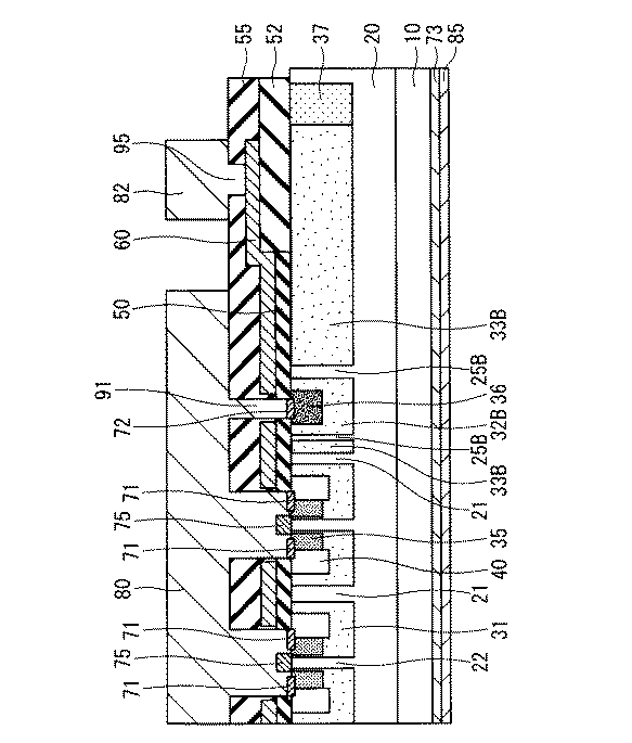
請求項1から請求項4のうちのいずれか1項に記載の半導体装置。 The width of the second well area and said third direction connecting the well area of the divided area is W, the effective impurity concentration of said divided area N, a dielectric constant of the semiconductor epsilon, the elementary charge If q
The semiconductor device according to claim 1 .
請求項1から請求項5のうちのいずれか1項に記載の半導体装置。 The divided area in a plan view, surrounds the second ohmic electrodes,
The semiconductor device according to any one of claims 1 to 5 .
前記第2のウェル領域の表層から深さ方向に貫通して設けられる、第1の導電型の第2の離間領域と、
前記第2の離間領域の上面に設けられる第2のショットキー電極とを備える、
請求項1から請求項6のうちのいずれか1項に記載の半導体装置。 The semiconductor device further includes:
It said provided second penetrating in the depth direction from the surface of the well area, and a second spaced area of the first conductivity type,
And a second Schottky electrodes provided on the upper surface of said second spaced area,
The semiconductor device according to claim 1 .
前記第3のウェル領域の上面の少なくとも一部に設けられるフィールド絶縁膜を備え、
前記フィールド絶縁膜の厚さは、前記ゲート絶縁膜の厚さよりも厚く、
前記ゲート電極は、前記フィールド絶縁膜が設けられる領域においては、前記フィールド絶縁膜を挟んで前記第3のウェル領域の上面に設けられる、
請求項4に記載の半導体装置。 The semiconductor device further includes:
Comprising a field insulating film provided on at least a portion of the upper surface of the third well area,
The field insulating film is thicker than the gate insulating film ,
The gate electrodes, in the region where the field insulating film is provided, is provided on the upper surface of the third well area across the field insulating film,
The semiconductor device according to claim 4 .
請求項8に記載の半導体装置。 The gate electrodes, the in the third region corresponding to the upper surface of the well area of, is provided on the upper surface of the third well area across the field insulating film,
The semiconductor device according to claim 8 .
前記第3のウェル領域の表層に設けられる、第2の導電型のウェル注入領域を備え、
前記ウェル注入領域の不純物濃度は、前記第1のウェル領域の不純物濃度よりも高い、
請求項1から請求項9のうちのいずれか1項に記載の半導体装置。 The semiconductor device further includes:
Provided on the surface layer of the third well area comprises a well implantation area of a second conductivity type,
The impurity concentration of the well implantation area is higher than the impurity concentration of said first well area,
The semiconductor device according to claim 1 .
前記分断領域の表層に設けられる、少なくとも1つの第2の導電型の補助導電領域を備え、
前記補助導電領域は、前記第2のウェル領域と第3のウェル領域とを電気的に接続する、
請求項1から請求項10のうちのいずれか1項に記載の半導体装置。 The semiconductor device further includes:
Provided on the surface layer of the cutting area, an auxiliary conductive area of at least one of the second conductivity type,
The auxiliary conductive area is electrically connecting the second well area and the third well area,
The semiconductor device according to claim 1 .
前記補助導電領域が設けられる長さは、前記補助導電領域が、前記第2のウェル領域と前記第3のウェル領域とを結ぶ方向と交差する方向において設けられる長さであり、
前記分断領域が設けられる長さは、前記分断領域が、前記第2のウェル領域と前記第3のウェル領域とを結ぶ方向と交差する方向において設けられる長さである、
請求項11に記載の半導体装置。 The total length of the auxiliary conductive area is provided is less than 1/10 of the total length of the cutting area is provided,
Length of the auxiliary conductive area is provided, the auxiliary conductive area is a length which is provided in the direction crossing the second well area and said third direction connecting the well area,
Length of the cutting area is provided, the divided area is a length which is provided in the direction crossing the second well area and said third direction connecting the well area,
The semiconductor device of claim 1 1.
Applications Claiming Priority (1)
| Application Number | Priority Date | Filing Date | Title |
|---|---|---|---|
| PCT/JP2016/061706 WO2017179102A1 (en) | 2016-04-11 | 2016-04-11 | Semiconductor device |
Related Child Applications (1)
| Application Number | Title | Priority Date | Filing Date |
|---|---|---|---|
| JP2019132446A Division JP6752336B2 (en) | 2019-07-18 | 2019-07-18 | Semiconductor device |
Publications (2)
| Publication Number | Publication Date |
|---|---|
| JPWO2017179102A1 JPWO2017179102A1 (en) | 2018-08-30 |
| JP6560444B2 true JP6560444B2 (en) | 2019-08-14 |
Family
ID=60042498
Family Applications (1)
| Application Number | Title | Priority Date | Filing Date |
|---|---|---|---|
| JP2018511559A Active JP6560444B2 (en) | 2016-04-11 | 2016-04-11 | Semiconductor device |
Country Status (5)
| Country | Link |
|---|---|
| US (1) | US11222973B2 (en) |
| JP (1) | JP6560444B2 (en) |
| CN (1) | CN108886038B (en) |
| DE (1) | DE112016006723T5 (en) |
| WO (1) | WO2017179102A1 (en) |
Families Citing this family (8)
| Publication number | Priority date | Publication date | Assignee | Title |
|---|---|---|---|---|
| JP6293380B1 (en) | 2016-04-21 | 2018-03-14 | 三菱電機株式会社 | Semiconductor device |
| WO2018037701A1 (en) * | 2016-08-25 | 2018-03-01 | 三菱電機株式会社 | Semiconductor device |
| CN115274855A (en) | 2017-02-24 | 2022-11-01 | 三菱电机株式会社 | Silicon carbide semiconductor device and power conversion device |
| WO2019124378A1 (en) * | 2017-12-19 | 2019-06-27 | 三菱電機株式会社 | Silicon carbide semiconductor device and power converter |
| WO2019124384A1 (en) | 2017-12-19 | 2019-06-27 | 三菱電機株式会社 | Silicon carbide semiconductor device and power conversion device |
| WO2019123717A1 (en) | 2017-12-19 | 2019-06-27 | 三菱電機株式会社 | Silicon carbide semiconductor device and power conversion device |
| WO2021044624A1 (en) * | 2019-09-06 | 2021-03-11 | 三菱電機株式会社 | Silicon carbide semiconductor device and power conversion device |
| US20230142729A1 (en) * | 2021-11-08 | 2023-05-11 | Analog Devices, Inc. | Integrated device package with an integrated heat sink |
Family Cites Families (19)
| Publication number | Priority date | Publication date | Assignee | Title |
|---|---|---|---|---|
| JP2858404B2 (en) * | 1990-06-08 | 1999-02-17 | 株式会社デンソー | Insulated gate bipolar transistor and method of manufacturing the same |
| JP3850580B2 (en) * | 1999-03-30 | 2006-11-29 | 株式会社東芝 | Semiconductor device |
| JP4538870B2 (en) * | 1999-09-21 | 2010-09-08 | 株式会社デンソー | Silicon carbide semiconductor device and manufacturing method thereof |
| JP5011612B2 (en) * | 2000-10-31 | 2012-08-29 | 富士電機株式会社 | Semiconductor device |
| JP2003017701A (en) | 2001-07-04 | 2003-01-17 | Denso Corp | Semiconductor device |
| JP4338178B2 (en) | 2003-03-24 | 2009-10-07 | 財団法人電力中央研究所 | Silicon carbide semiconductor device inspection method and inspection device, and silicon carbide semiconductor device manufacturing method |
| JP4585772B2 (en) * | 2004-02-06 | 2010-11-24 | 関西電力株式会社 | High breakdown voltage wide gap semiconductor device and power device |
| DE112009004277T5 (en) * | 2008-12-25 | 2012-10-04 | Mitsubishi Electric Corp. | POWER SEMICONDUCTOR DEVICE |
| KR101291838B1 (en) * | 2009-10-14 | 2013-07-31 | 미쓰비시덴키 가부시키가이샤 | Power semiconductor device |
| WO2011161721A1 (en) * | 2010-06-24 | 2011-12-29 | 三菱電機株式会社 | Power semiconductor device |
| WO2012001837A1 (en) * | 2010-06-30 | 2012-01-05 | 三菱電機株式会社 | Power semiconductor device |
| JP5159987B1 (en) | 2011-10-03 | 2013-03-13 | パナソニック株式会社 | Semiconductor device, power converter, and control method of power converter |
| JP6072432B2 (en) * | 2012-05-15 | 2017-02-01 | 三菱電機株式会社 | Semiconductor device and manufacturing method thereof |
| CN104620381B (en) | 2012-09-06 | 2017-04-19 | 三菱电机株式会社 | Semiconductor device |
| WO2014162969A1 (en) * | 2013-04-03 | 2014-10-09 | 三菱電機株式会社 | Semiconductor device |
| JP5939448B2 (en) * | 2013-04-30 | 2016-06-22 | 日産自動車株式会社 | Semiconductor device and manufacturing method thereof |
| JP6244762B2 (en) * | 2013-09-12 | 2017-12-13 | 住友電気工業株式会社 | Silicon carbide semiconductor device |
| US9224816B2 (en) * | 2014-05-21 | 2015-12-29 | Sumitomo Electric Industries, Ltd. | Silicon carbide semiconductor device |
| WO2016170706A1 (en) * | 2015-04-22 | 2016-10-27 | 三菱電機株式会社 | Semiconductor device and semiconductor device manufacturing method |
-
2016
- 2016-04-11 WO PCT/JP2016/061706 patent/WO2017179102A1/en active Application Filing
- 2016-04-11 CN CN201680084166.3A patent/CN108886038B/en active Active
- 2016-04-11 DE DE112016006723.2T patent/DE112016006723T5/en active Pending
- 2016-04-11 US US16/082,212 patent/US11222973B2/en active Active
- 2016-04-11 JP JP2018511559A patent/JP6560444B2/en active Active
Also Published As
| Publication number | Publication date |
|---|---|
| US11222973B2 (en) | 2022-01-11 |
| WO2017179102A1 (en) | 2017-10-19 |
| CN108886038B (en) | 2023-05-02 |
| JPWO2017179102A1 (en) | 2018-08-30 |
| DE112016006723T5 (en) | 2018-12-20 |
| CN108886038A (en) | 2018-11-23 |
| US20190181259A1 (en) | 2019-06-13 |
Similar Documents
| Publication | Publication Date | Title |
|---|---|---|
| JP6560444B2 (en) | Semiconductor device | |
| US7700971B2 (en) | Insulated gate silicon carbide semiconductor device | |
| US7781786B2 (en) | Semiconductor device having a heterojunction diode and manufacturing method thereof | |
| JP5940235B1 (en) | Semiconductor device | |
| US8933466B2 (en) | Semiconductor element | |
| JP2019054064A (en) | Semiconductor device | |
| US20080197361A1 (en) | Insulated gate silicon carbide semiconductor device and method for manufacturing the same | |
| JP6649183B2 (en) | Semiconductor device | |
| CN109564942B (en) | Semiconductor device with a plurality of semiconductor chips | |
| JP2016006854A (en) | Semiconductor element and manufacturing method thereof | |
| JP2019071313A (en) | Semiconductor device | |
| JP7176239B2 (en) | semiconductor equipment | |
| US9029874B2 (en) | Semiconductor device having a first silicon carbide semiconductor layer and a second silicon carbide semiconductor layer | |
| JP2017069551A (en) | Semiconductor element | |
| US20230017518A1 (en) | Semiconductor device | |
| JP2019216223A (en) | Semiconductor device | |
| JP5098293B2 (en) | Insulated gate type semiconductor device using wide band gap semiconductor and manufacturing method thereof | |
| CN112466922A (en) | Semiconductor device with a plurality of semiconductor chips | |
| JP6752336B2 (en) | Semiconductor device | |
| JP2022007788A (en) | Semiconductor device | |
| CN112466923A (en) | Semiconductor device with a plurality of semiconductor chips | |
| JP7196265B2 (en) | semiconductor equipment | |
| US20220336590A1 (en) | Silicon carbide semiconductor device and method for manufacturing the same | |
| US20220246729A1 (en) | Silicon carbide vertical conduction mosfet device and manufacturing process thereof | |
| US20220246723A1 (en) | Silicon carbide vertical conduction mosfet device for power applications and manufacturing process thereof |
Legal Events
| Date | Code | Title | Description |
|---|---|---|---|
| A521 | Request for written amendment filed | ||
| A621 | Written request for application examination | ||
| TRDD | Decision of grant or rejection written | ||
| A01 | Written decision to grant a patent or to grant a registration (utility model) |
Free format text: JAPANESE INTERMEDIATE CODE: A01 Effective date: 20190618 |
|
| A61 | First payment of annual fees (during grant procedure) |
Free format text: JAPANESE INTERMEDIATE CODE: A61 Effective date: 20190718 |
|
| R150 | Certificate of patent or registration of utility model |
Ref document number: 6560444 Country of ref document: JP Free format text: JAPANESE INTERMEDIATE CODE: R150 |
|
| R250 | Receipt of annual fees |
Free format text: JAPANESE INTERMEDIATE CODE: R250 |
|
| R250 | Receipt of annual fees |
Free format text: JAPANESE INTERMEDIATE CODE: R250 |