WO2017130778A1 - パワー半導体装置及びパワー半導体装置の製造方法 - Google Patents
パワー半導体装置及びパワー半導体装置の製造方法 Download PDFInfo
- Publication number
- WO2017130778A1 WO2017130778A1 PCT/JP2017/001288 JP2017001288W WO2017130778A1 WO 2017130778 A1 WO2017130778 A1 WO 2017130778A1 JP 2017001288 W JP2017001288 W JP 2017001288W WO 2017130778 A1 WO2017130778 A1 WO 2017130778A1
- Authority
- WO
- WIPO (PCT)
- Prior art keywords
- region
- conductivity type
- semiconductor device
- power semiconductor
- trench
- Prior art date
- Legal status (The legal status is an assumption and is not a legal conclusion. Google has not performed a legal analysis and makes no representation as to the accuracy of the status listed.)
- Ceased
Links
Images







Classifications
-
- H—ELECTRICITY
- H10—SEMICONDUCTOR DEVICES; ELECTRIC SOLID-STATE DEVICES NOT OTHERWISE PROVIDED FOR
- H10D—INORGANIC ELECTRIC SEMICONDUCTOR DEVICES
- H10D30/00—Field-effect transistors [FET]
- H10D30/60—Insulated-gate field-effect transistors [IGFET]
- H10D30/64—Double-diffused metal-oxide semiconductor [DMOS] FETs
- H10D30/66—Vertical DMOS [VDMOS] FETs
- H10D30/668—Vertical DMOS [VDMOS] FETs having trench gate electrodes, e.g. UMOS transistors
-
- H—ELECTRICITY
- H10—SEMICONDUCTOR DEVICES; ELECTRIC SOLID-STATE DEVICES NOT OTHERWISE PROVIDED FOR
- H10D—INORGANIC ELECTRIC SEMICONDUCTOR DEVICES
- H10D12/00—Bipolar devices controlled by the field effect, e.g. insulated-gate bipolar transistors [IGBT]
- H10D12/01—Manufacture or treatment
- H10D12/031—Manufacture or treatment of IGBTs
- H10D12/032—Manufacture or treatment of IGBTs of vertical IGBTs
- H10D12/035—Etching a recess in the emitter region
-
- H—ELECTRICITY
- H10—SEMICONDUCTOR DEVICES; ELECTRIC SOLID-STATE DEVICES NOT OTHERWISE PROVIDED FOR
- H10D—INORGANIC ELECTRIC SEMICONDUCTOR DEVICES
- H10D12/00—Bipolar devices controlled by the field effect, e.g. insulated-gate bipolar transistors [IGBT]
- H10D12/01—Manufacture or treatment
- H10D12/031—Manufacture or treatment of IGBTs
- H10D12/032—Manufacture or treatment of IGBTs of vertical IGBTs
- H10D12/038—Manufacture or treatment of IGBTs of vertical IGBTs having a recessed gate, e.g. trench-gate IGBTs
-
- H—ELECTRICITY
- H10—SEMICONDUCTOR DEVICES; ELECTRIC SOLID-STATE DEVICES NOT OTHERWISE PROVIDED FOR
- H10D—INORGANIC ELECTRIC SEMICONDUCTOR DEVICES
- H10D12/00—Bipolar devices controlled by the field effect, e.g. insulated-gate bipolar transistors [IGBT]
- H10D12/411—Insulated-gate bipolar transistors [IGBT]
- H10D12/441—Vertical IGBTs
- H10D12/461—Vertical IGBTs having non-planar surfaces, e.g. having trenches, recesses or pillars in the surfaces of the emitter, base or collector regions
- H10D12/481—Vertical IGBTs having non-planar surfaces, e.g. having trenches, recesses or pillars in the surfaces of the emitter, base or collector regions having gate structures on slanted surfaces, on vertical surfaces, or in grooves, e.g. trench gate IGBTs
-
- H—ELECTRICITY
- H10—SEMICONDUCTOR DEVICES; ELECTRIC SOLID-STATE DEVICES NOT OTHERWISE PROVIDED FOR
- H10D—INORGANIC ELECTRIC SEMICONDUCTOR DEVICES
- H10D30/00—Field-effect transistors [FET]
- H10D30/01—Manufacture or treatment
- H10D30/021—Manufacture or treatment of FETs having insulated gates [IGFET]
- H10D30/028—Manufacture or treatment of FETs having insulated gates [IGFET] of double-diffused metal oxide semiconductor [DMOS] FETs
- H10D30/0291—Manufacture or treatment of FETs having insulated gates [IGFET] of double-diffused metal oxide semiconductor [DMOS] FETs of vertical DMOS [VDMOS] FETs
- H10D30/0295—Manufacture or treatment of FETs having insulated gates [IGFET] of double-diffused metal oxide semiconductor [DMOS] FETs of vertical DMOS [VDMOS] FETs using recessing of the source electrodes
-
- H—ELECTRICITY
- H10—SEMICONDUCTOR DEVICES; ELECTRIC SOLID-STATE DEVICES NOT OTHERWISE PROVIDED FOR
- H10D—INORGANIC ELECTRIC SEMICONDUCTOR DEVICES
- H10D30/00—Field-effect transistors [FET]
- H10D30/01—Manufacture or treatment
- H10D30/021—Manufacture or treatment of FETs having insulated gates [IGFET]
- H10D30/028—Manufacture or treatment of FETs having insulated gates [IGFET] of double-diffused metal oxide semiconductor [DMOS] FETs
- H10D30/0291—Manufacture or treatment of FETs having insulated gates [IGFET] of double-diffused metal oxide semiconductor [DMOS] FETs of vertical DMOS [VDMOS] FETs
- H10D30/0297—Manufacture or treatment of FETs having insulated gates [IGFET] of double-diffused metal oxide semiconductor [DMOS] FETs of vertical DMOS [VDMOS] FETs using recessing of the gate electrodes, e.g. to form trench gate electrodes
-
- H—ELECTRICITY
- H10—SEMICONDUCTOR DEVICES; ELECTRIC SOLID-STATE DEVICES NOT OTHERWISE PROVIDED FOR
- H10D—INORGANIC ELECTRIC SEMICONDUCTOR DEVICES
- H10D62/00—Semiconductor bodies, or regions thereof, of devices having potential barriers
- H10D62/01—Manufacture or treatment
- H10D62/051—Forming charge compensation regions, e.g. superjunctions
- H10D62/058—Forming charge compensation regions, e.g. superjunctions by using trenches, e.g. implanting into sidewalls of trenches or refilling trenches
-
- H—ELECTRICITY
- H10—SEMICONDUCTOR DEVICES; ELECTRIC SOLID-STATE DEVICES NOT OTHERWISE PROVIDED FOR
- H10D—INORGANIC ELECTRIC SEMICONDUCTOR DEVICES
- H10D62/00—Semiconductor bodies, or regions thereof, of devices having potential barriers
- H10D62/10—Shapes, relative sizes or dispositions of the regions of the semiconductor bodies; Shapes of the semiconductor bodies
- H10D62/102—Constructional design considerations for preventing surface leakage or controlling electric field concentration
- H10D62/103—Constructional design considerations for preventing surface leakage or controlling electric field concentration for increasing or controlling the breakdown voltage of reverse-biased devices
- H10D62/105—Constructional design considerations for preventing surface leakage or controlling electric field concentration for increasing or controlling the breakdown voltage of reverse-biased devices by having particular doping profiles, shapes or arrangements of PN junctions; by having supplementary regions, e.g. junction termination extension [JTE]
- H10D62/109—Reduced surface field [RESURF] PN junction structures
- H10D62/111—Multiple RESURF structures, e.g. double RESURF or 3D-RESURF structures
-
- H—ELECTRICITY
- H10—SEMICONDUCTOR DEVICES; ELECTRIC SOLID-STATE DEVICES NOT OTHERWISE PROVIDED FOR
- H10D—INORGANIC ELECTRIC SEMICONDUCTOR DEVICES
- H10D64/00—Electrodes of devices having potential barriers
- H10D64/20—Electrodes characterised by their shapes, relative sizes or dispositions
- H10D64/23—Electrodes carrying the current to be rectified, amplified, oscillated or switched, e.g. sources, drains, anodes or cathodes
- H10D64/251—Source or drain electrodes for field-effect devices
- H10D64/256—Source or drain electrodes for field-effect devices for lateral devices wherein the source or drain electrodes are recessed in semiconductor bodies
Definitions
- the present invention relates to a power semiconductor device and a method for manufacturing the power semiconductor device.
- a power MOSFET that electrically connects a source electrode and a source region via a metal plug can be considered (see Power MOSFET 900 according to Background Art, FIG. 22). (For example, refer to Patent Document 1 as a semiconductor device).
- a power MOSFET 900 includes a low-resistance semiconductor layer 912, a drift layer 914 formed on the low-resistance semiconductor layer 912, a p-type base region 918 formed on the surface of the drift layer 914, and a base region
- a semiconductor substrate 910 having a source region 920 formed on the surface of 918, and a depth position reaching the drift layer 914 through the base region 918, and a part of the source region 920 is exposed to the inner peripheral surface
- a plurality of trenches 922 formed in such a manner, a gate insulating film 924 formed on the inner peripheral surface of the trench 922, a gate electrode 926 embedded in the trench 922 through the gate insulating film 924, a base
- An interlayer insulating film 928 covering the region 918, the source region 920, the gate insulating film 924, and the gate electrode 926 is adjacent to each other.
- Semiconductor body 910 is in contact with the bottom surface of the metal plug 932, and is electrically connected to the source electrode 936 via the metal plug 932, and a high p + -type high concentration impurity concentration than the base region 918 It further has a diffusion region 934.
- the power MOSFET 900 according to the background art is a power MOSFET that meets the demand for cost reduction and miniaturization of electronic devices.
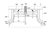
- one metal plug 932 having a relatively small diameter is formed between two trenches 922 adjacent to each other. Therefore, the distance d2 between the trench 922 and the p + -type high concentration diffusion region 934 is relatively long when viewed in plan (see FIG. 23).
- the holes generated at the bottom of the trench 922 (which is a place where holes are relatively easily generated) Since a long distance is moved and a high potential difference is easily generated between the base region 918 and the metal plug 932, the source region 920 (n-type), the base region 918 (p-type), and the drift layer 914 (n-type) ) Is easily turned on (see FIG. 23). Further, (2) since the area of the “interface between the source region 920 and the base region 918” is increased and the holes of the base region 918 easily enter the source region 920, the parasitic npn transistor described above is also turned on from this viewpoint. (See FIG. 23).
- the present invention has been made to solve the above-described problems, and an object of the present invention is to provide a power semiconductor device that satisfies the demand for cost reduction and downsizing of electronic devices and has a high breakdown resistance. To do. Moreover, it aims at providing the manufacturing method of such a power semiconductor device.
- a power semiconductor device includes a low-resistance semiconductor layer, a plurality of first conductivity type column regions formed on the low-resistance semiconductor layer, and alternately formed along a predetermined direction, and a plurality of first semiconductor regions.
- Conductive type high concentration diffusion region A plurality of trenches that are partially exposed on the inner peripheral surface, a gate insulating film formed on the inner peripheral surface of the trench, and embedded in the trench through the gate insulating film Two or more gate electrodes, two or more interlayer insulating films covering the base region, the first conductivity type high concentration diffusion region, the gate insulating film and the gate electrode, and two trenches adjacent
- an electrode electrically connected to the base region and the first conductivity type high concentration diffusion region, and the semiconductor substrate is in contact with a bottom surface of the metal plug.
- a second conductivity type high concentration diffusion region that is electrically connected to the electrode through the metal plug and has an impurity concentration higher than that of the base region.
- the one-conductivity type high-concentration diffusion region is formed between the two adjacent trenches and only between the trench and the metal plug closest to the trench.
- two trenches adjacent to each other is a concept including not only the case where the trenches are viewed as a whole but also the case where the trenches are adjacent to each other when viewed from a predetermined cross section. For example, even when the trenches are in a lattice shape and the trenches are connected to each other, when adjacent to each other when viewed from a predetermined cut surface, the two adjacent trenches Shall be included. Further, in this specification, “between two adjacent trenches” includes not only a straight line between trenches in a plan view but also a case where the position is slightly deviated from the straight line. .
- the position where the metal plug closest to the trench and the first conductive type high concentration diffusion region are in contact between the two adjacent trenches is planar. In view of this, it is preferable to be outside the region where the second conductivity type column region is formed.
- the metal plug closest to the trench is formed with the second conductivity type column region in plan view. It is preferable that it is formed outside the region.
- the metal is preferably tungsten.
- the interval between the two adjacent gate electrodes is preferably 2.5 ⁇ m or more.
- the interval between the two adjacent gate electrodes is not less than 5 times the width of the metal plug.
- the contact hole is formed to a deeper position than a bottom surface of the first conductivity type high concentration diffusion region.
- the depth position of the deepest portion of the base region is preferably in the range of 0.5 ⁇ m to 2.0 ⁇ m.
- a method for manufacturing a power semiconductor device according to the present invention is a method for manufacturing a power semiconductor device according to any one of the above [1] to [8], wherein the low resistance semiconductor layer And a plurality of first conductivity type column regions and a plurality of second conductivity type column regions formed on the low-resistance semiconductor layer and alternately formed along a predetermined direction.
- a first conductivity type high concentration diffusion region in which a first conductivity type high concentration diffusion region is formed in a predetermined region of the surface of the base region so as to be exposed at least partially on the inner peripheral surface of the trench
- an interlayer insulating film forming step of forming an interlayer insulating film covering the base region, the first conductivity type high concentration diffusion region, the gate insulating film and the gate electrode, and between the two adjacent trenches
- the semiconductor substrate preparation step includes a low-resistance semiconductor layer and a first impurity layer formed on the low-resistance semiconductor layer and having a lower impurity concentration than the low-resistance semiconductor layer.
- a first step of preparing a semiconductor substrate on which a conductive semiconductor layer is laminated, and etching using an insulating film as a mask so as to be arranged along a predetermined direction on the surface of the first conductive semiconductor layer A second step of forming a plurality of second conductivity type column trenches having a predetermined depth by the second step, and a second step inside the second conductivity type column trenches to a height position exceeding the surface height of the insulating film.
- the power semiconductor device and the method for manufacturing the power semiconductor device according to the present invention include two or more contact holes formed between two adjacent trenches so as to pass through the interlayer insulating film and reach at least the base region, And a metal plug in which a metal is filled in the contact hole.
- the distance d1 between the trench and the second conductivity type high-concentration diffusion region in plan view is shorter than the distance d2 in the power MOSFET 900 according to the background art (see FIG. 8). . Therefore, (1) during the avalanche breakdown and the reverse recovery of the body diode, comparison is made between the carriers generated at the bottom of the trench (where carriers (for example, holes) are relatively likely to be generated) until they are extracted by the electrode.
- the first conductivity type high-concentration diffusion region for example, n-type
- the base region for example, p-type
- the first region A parasitic transistor (parasitic npn transistor) composed of one conductivity type column region (for example, n-type) is difficult to turn on (see FIG. 8).
- the area of the “boundary surface between the first conductivity type high concentration diffusion region and the base region” is narrowed, and carriers in the base region are difficult to enter the first conductivity type high concentration diffusion region.
- the parasitic transistor (parasitic npn transistor) described above is difficult to turn on (see FIG. 8). As a result, avalanche breakdown or di / dt breakdown is unlikely to occur, and a power semiconductor device having a large breakdown resistance can be obtained.
- the power semiconductor device and the method for manufacturing the power semiconductor device according to the present invention satisfy the demand for cost reduction and downsizing of the electronic equipment and have a large breakdown resistance.
- two or more contact holes are formed between two adjacent trenches, and the inside of the contact hole is filled with metal. Therefore, contact resistance is reduced as compared with a case where a contact hole formed between two adjacent trenches and a metal plug filled with metal inside the contact hole are provided. It becomes possible to do.
- the first conductivity type high concentration diffusion region is formed between the trench adjacent to each other and the metal plug closest to the trench.
- the area of the “interface between the first conductivity type high-concentration diffusion region and the base region” is narrowed, and carriers generated near the bottom of the trench in the first conductivity type column region ( Hole) is less likely to enter the first conductivity type high-concentration diffusion region, and the above-described parasitic npn transistor is more difficult to turn on more reliably.
- the semiconductor substrate having the super junction structure is formed in the n-type column region and the p-type column region, the low on-resistance and the high It becomes a withstand voltage switching element.
- the semiconductor substrate having the super junction structure is formed in the n-type column region and the p-type column region, such a high breakdown voltage is provided. Even a power semiconductor device can satisfy a demand for cost reduction and miniaturization of an electronic device and can be a power semiconductor device having a large breakdown resistance.
- the second semiconductor device at the time of avalanche breakdown and reverse recovery of the body diode.
- a large amount of carriers (holes) are generated in the conductive column region.
- carriers (holes) generated in the second conductivity type column region move toward the electrode (for example, source electrode) side, and pass through the second conductivity type high concentration diffusion region and the metal plug (for example, source). Electrode).
- the first conductivity type high concentration diffusion region is formed between two adjacent metal plugs between two adjacent trenches, the first conductivity type high concentration diffusion region occurs in the second conductivity type column region.
- the semiconductor substrate having a super junction structure in the first conductivity type column region and the second conductivity type column region is provided.
- the one-conductivity type high-concentration diffusion region is formed between two adjacent trenches only between the trench and the metal plug closest to the trench, carriers generated in the second-conductivity type column region ( Hole) does not move near the first conductivity type high concentration diffusion region, and carriers (holes) do not enter the first conductivity type high concentration diffusion region. Therefore, a parasitic element composed of a first conductivity type high-concentration diffusion region (for example, n-type), a base region (for example, p-type) and a first conductivity type column region (for example, n-type) between two adjacent metal plugs. The transistor (parasitic npn transistor) is not turned on.
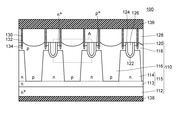
- FIG. 1 is a cross-sectional view of a power semiconductor device 100 according to Embodiment 1.
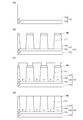
- FIG. FIG. 6 is a cross-sectional view for explaining the method for manufacturing the power semiconductor device according to the first embodiment.
- 2A to 2D are process diagrams.
- FIG. 6 is a cross-sectional view for explaining the method for manufacturing the power semiconductor device according to the first embodiment.
- 3A to 3D are process diagrams.
- FIG. 6 is a cross-sectional view for explaining the method for manufacturing the power semiconductor device according to the first embodiment.
- FIGS. 5A to 5C are process diagrams.
- FIG. 6 is a cross-sectional view for explaining the method for manufacturing the power semiconductor device according to the first embodiment.
- FIG. 6A to FIG. 6C are process diagrams.
- FIG. 6 is a cross-sectional view for explaining the method for manufacturing the power semiconductor device according to the first embodiment.
- FIG. 7A to FIG. 7C are process diagrams.
- FIG. 8 corresponds to the area surrounded by the broken line A in FIG. 1 (the same applies to FIGS. 8 and 10). In FIG. 8, white circles indicate holes.
- the power semiconductor device 700 according to the comparative example 1 is the power semiconductor according to the first embodiment except that the semiconductor substrate having the n-type drift layer 714 is provided instead of the semiconductor substrate having the super junction structure. This is a power semiconductor device having the same configuration as the device 100.
- FIG. 4 is an enlarged cross-sectional view of a main part shown for explaining the effect of the power semiconductor device 100 according to the first embodiment.
- 11A is a diagram showing the state of the surface of the semiconductor substrate immediately before the source region forming step when the source region is formed also in the region where the p-type column region is formed in plan view.
- 11B the source region when the metal plug closest to the trench is formed inside the region where the p-type column region is formed between two trenches adjacent to each other in plan view.
- FIG. 11C is a diagram illustrating a state of the surface of the semiconductor substrate after the formation step is performed
- FIG. 11C is a diagram illustrating a state of the surface of the semiconductor substrate after the metal plug formation step is performed in the first embodiment.
- 11A to 11C are diagrams corresponding to the area surrounded by the broken line B in FIG. 5B.
- FIG. 11B also shows a metal plug 132 formed in the metal plug forming step. Furthermore, in FIG. 11, the symbol G indicates a particle.
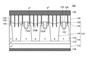
- FIG. 6 is a cross-sectional view of a power semiconductor device 102 according to a second embodiment.
- FIG. 5 is a cross-sectional view of a power semiconductor device 104 according to a third embodiment.
- FIG. 3 is an enlarged plan view of a main part of the power semiconductor device 100 according to the first embodiment.
- the trench 122 and the metal plug 132 are both striped when viewed in plan.
- the source electrode and the interlayer insulating film are not shown (the same applies to FIGS. 15 to 19).
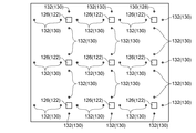
- 10 is an enlarged plan view of a main part of a power semiconductor device according to Modification 1.
- the trench 122 has a lattice shape when viewed in plan
- the metal plug 132 has a circular shape when viewed in plan (column shape when viewed in three dimensions).
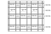
- 10 is an enlarged plan view of a main part of a power semiconductor device according to Modification 2.
- the trench 122 has a lattice shape when viewed in plan, and the metal plug 132 has a rectangular frame shape when viewed in plan.
- 10 is an enlarged plan view of a main part of a power semiconductor device according to Modification 3.
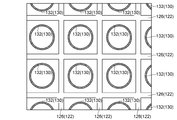
- FIG. 11 is an enlarged plan view of a main part of a power semiconductor device according to Modification 4.
- the trench 122 has a quadrangular shape (columnar shape when viewed three-dimensionally) as viewed in a plan view, and the metal plug 132 has a lattice shape when viewed in plan view.
- FIG. 10 is an enlarged plan view of a main part of a power semiconductor device 106 according to Modification 5.
- the trench 122 has a quadrangular shape (a columnar shape when viewed three-dimensionally) when viewed in plan, and the metal plug 132 is a circular shape (when viewed three-dimensionally). It is columnar to see).
- FIG. 10 is a cross-sectional view of a power semiconductor device 106 according to Modification 6.
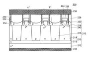
- FIG. 11 is a cross-sectional view of a power semiconductor device 200 according to Modification 7.
- Reference numeral 210 indicates a semiconductor substrate
- reference numeral 212 indicates a low-resistance semiconductor layer
- reference numeral 213 indicates a buffer layer
- reference numeral 214 indicates an n-type column region
- reference numeral 215 indicates an n-type semiconductor layer
- reference numeral 216 indicates an n-type semiconductor layer
- reference numeral 218 indicates a base region
- reference numeral 220 indicates a source region
- reference numeral 224 indicates a gate insulating film
- reference numeral 226 indicates a gate electrode
- reference numeral 228 indicates an interlayer insulating film
- Reference numeral 230 indicates a contact hole
- reference numeral 232 indicates a metal plug
- reference numeral 234 indicates a p + -type diffusion region
- reference numeral 236 indicates a source electrode
- reference numeral 238 indicates a drain electrode
- reference numeral 240 indicates a high-concentration surface diffusion. Indicates the area. It is sectional drawing of power MOSFET900 which concerns on background art.
- FIG. 23 corresponds to the area surrounded by the broken line C in FIG.
- white circles indicate holes and black circles indicate electrons.
- Embodiment 1 Configuration of Power Semiconductor Device 100 According to Embodiment 1
- the power semiconductor device 100 according to Embodiment 1 is a trench gate power MOSFET used for various power supply devices such as a DC-DC converter.
- the breakdown voltage of the power semiconductor device 100 according to the first embodiment is 300V or more, for example, 600V.
- the power semiconductor device 100 includes a semiconductor substrate 110, a plurality of trenches 122, a gate insulating film 124, a gate electrode 126, an interlayer insulating film 128, and a contact hole 130.
- the semiconductor substrate 110 includes a low-resistance semiconductor layer 112, a buffer layer 113 formed on the low-resistance semiconductor layer 112, and a plurality of n formed alternately on the buffer layer 113 along a predetermined direction. Formed on the surfaces of the type column region 114 (first conductivity type column region) and the plurality of p type column regions 116 (second conductivity type column region), and the plurality of n type column regions 114 and the plurality of p type column regions 116 The p-type base region 118, the source region 120 (first conductivity type high concentration diffusion region) disposed on the surface of the base region 118, the bottom surface of the metal plug 132, and the metal plug 132 The p + -type diffusion region 134 (second conductivity type high-concentration extension) is electrically connected to the base region 118 and the source region 120 via the gate electrode and has a higher impurity concentration than the base region 118 A plurality of n-type column regions 114 and a plurality of p-type
- the total amount of impurities in the n-type column region 114 is equal to the total amount of impurities in the p-type column region 116 (impurity of impurities in the p-type column region). It is formed to be equal to the total amount). That is, the n-type column region 114 and the p-type column region 116 are in charge balance.
- a recess is formed on the surface of the semiconductor substrate 110 in the entire region where the p-type column region 116 is formed and a part of the region where the n-type column region 114 is formed as viewed in a plan view.
- the source region 120 is formed only between the trench 122 and the metal plug 132 closest to the trench 122 between two adjacent trenches 122.
- the source region 120 is formed only in the n-type column region, and one end portion is in contact with the trench 122 and the other end portion is in contact with the metal plug 132.
- each of the p-type column region 116 and the source region 120 has a stripe shape when seen in a plan view, but has a circular shape (a columnar shape when seen in a three-dimensional view). ), A rectangular frame shape, a circular frame shape, a lattice shape, or the like.
- the thickness of the low resistance semiconductor layer 112 is, for example, in the range of 100 ⁇ m to 400 ⁇ m, and the impurity concentration of the low resistance semiconductor layer 112 is, for example, in the range of 1 ⁇ 10 19 cm ⁇ 3 to 1 ⁇ 10 20 cm ⁇ 3. is there.
- the thickness of the n-type semiconductor layer 115 is, for example, in the range of 5 ⁇ m to 120 ⁇ m, and the impurity concentration of the n-type semiconductor layer 115 is, for example, in the range of 5 ⁇ 10 13 cm ⁇ 3 to 1 ⁇ 10 16 cm ⁇ 3. .
- the depth position of the deepest part of the base region 118 is within a range of 0.5 ⁇ m to 2.0 ⁇ m, for example, and the impurity concentration of the base region 118 is, for example, 5 ⁇ 10 16 cm ⁇ 3 to 1 ⁇ 10 18 cm ⁇ 3. It is in the range.
- the depth position of the deepest part of the source region 120 is in the range of 0.1 ⁇ m to 0.4 ⁇ m, for example, and the impurity concentration of the source region 120 is, for example, 5 ⁇ 10 19 cm ⁇ 3 to 2 ⁇ 10 20 cm ⁇ 3. It is in the range.
- the impurity concentration of the p + -type diffusion region 134 is higher than the impurity concentration of the base region 118 and is, for example, in the range of 5 ⁇ 10 18 cm ⁇ 3 to 1 ⁇ 10 20 cm ⁇ 3 .
- the plurality of trenches 122 are formed in a region where the n-type column region 114 is formed in a plan view up to a depth that passes through the base region 118 and reaches the n-type column region 114, and the source region 120. Is partly exposed on the inner peripheral surface.
- the depth of the trench 122 is, for example, 3 ⁇ m.
- the gate insulating film 124 is formed on the inner peripheral surface of the trench 122.
- the gate electrode 126 is embedded in the trench 122 through the gate insulating film 124.
- the interlayer insulating film 128 covers the base region 118, the source region 120, the gate insulating film 124, and the gate electrode 126.
- the gate insulating film 124 is made of a silicon dioxide film formed by a thermal oxidation method and has a thickness of 100 nm, for example.
- the gate electrode 126 is made of low resistance polysilicon formed by a CVD method and an ion implantation method.
- the interlayer insulating film 128 includes a thermal oxide film and a PSG film formed by a CVD method, and has a thickness of, for example, 1000 nm.
- Two or more contact holes 130 are formed between the two adjacent trenches 122 (two in the first embodiment) so as to penetrate through the interlayer insulating film 128 and reach at least the base region 118.
- the metal plug 132 is formed by filling the contact hole 130 with metal.
- the contact hole 130 and the metal plug 132 are formed to reach a depth position deeper than the depth position of the bottom of the source region 120 from the depth position of the surface of the base region 118.
- the stripe width of the contact hole 130 and the metal plug 132 is, for example, 0.5 ⁇ m.
- a barrier metal (not shown) is formed on the inner surface of the contact hole 130, and the metal plug 132 is filled with metal inside the contact hole 130 through the barrier metal.
- the metal filling the contact hole 130 is, for example, tungsten.
- the trench 122, the gate electrode 126, the contact hole 130, and the metal plug 132 are all formed in a stripe shape when seen in a plan view.
- the interval between two gate electrodes 126 adjacent to each other is 5 times or more the width (stripe width) of the metal plug 132.
- the interval (pitch width) between two gate electrodes 126 adjacent to each other is, for example, 2.5 ⁇ m or more, for example, 10 ⁇ m.
- the metal plugs 132 are formed at equal intervals, and the interval between any one of the two trenches 122 and the metal plug 132 closest to the trench is as follows. , Equal to the interval between two metal plugs 132 adjacent to each other. With such a configuration, there is an effect that it is easy to alleviate the concentration of the electric field at the bottom of each trench 122 during reverse bias.
- the interval between the metal plugs 132 is equal to or longer than the stripe width of the metal plugs 132, and is, for example, 0.5 ⁇ m or more.
- the metal plug 132 closest to the trench 122 (gate electrode 126) is formed outside the region where the p-type column region 116 is formed in plan view. Therefore, the position where the metal plug 132 closest to the trench 122 and the source region 120 are in contact with each other between the two adjacent trenches 122 is outside the region where the p-type column region 116 is formed in plan view. It is.
- the source electrode 136 is formed on the interlayer insulating film 128 and is electrically connected to the base region 118 and the source region 120 through the metal plug 132.
- the drain electrode 138 is formed on the surface of the low resistance semiconductor layer 112.
- the source electrode 136 is made of an aluminum-based metal (for example, an Al—Cu alloy) having a thickness of, for example, 4 ⁇ m formed by sputtering.
- the drain electrode 138 is formed of a multilayer metal film such as Ti—Ni—Au, and has a thickness of, for example, 0.5 ⁇ m over the entire multilayer metal film.
- the power semiconductor device 100 according to Embodiment 1 is manufactured by a manufacturing method (a manufacturing method of a power semiconductor device according to Embodiment 1) having manufacturing steps shown below. be able to.
- the method for manufacturing a power semiconductor device according to the first embodiment includes a semiconductor substrate preparation step, a trench formation step, a gate electrode formation step, a base region formation step, and a source region formation step (first conductivity type high concentration diffusion region formation). Step), interlayer insulating film forming step, contact hole forming step, p + type diffusion region forming step (second conductivity type high concentration diffusion region forming step), metal plug filling step, and electrode forming step. Include in order.
- a semiconductor substrate 110 having a region 116 and having a super junction structure constituted by a plurality of n-type column regions 114 and a plurality of p-type column regions 116 is prepared. Specifically, the semiconductor substrate 110 is prepared by performing the following steps.
- a low-resistance semiconductor layer 112 and an n-type semiconductor layer 115 formed on the low-resistance semiconductor layer 112 and having an impurity concentration lower than that of the low-resistance semiconductor layer 112 (first conductive semiconductor layer) ) Is prepared (see FIG. 2A).
- the semiconductor substrate 110 an appropriate semiconductor substrate can be used.
- a semiconductor substrate in which an n ⁇ type n-type semiconductor layer 115 is formed on an n + type low-resistance semiconductor layer 112 by epitaxial growth is used. be able to.
- a plurality of p-type columns having a predetermined depth are etched by using the insulating film M1 as a mask so as to be arranged in a predetermined direction on the surface of the n-type semiconductor layer 115.
- a trench 117 (second conductivity type column trench) is formed (see FIG. 2B).
- the thickness of the insulating film M1 can be set to an appropriate thickness.
- a buffer layer 113 is formed from the depth position of the p-type column trench 117 to the depth position of the boundary surface between the low-resistance semiconductor layer 112 and the n-type semiconductor layer 115.
- the p-type semiconductor material (second conductivity type semiconductor material) is epitaxially grown inside the p-type column trench 117 to a height position exceeding the surface height of the insulating film M1.
- a p-type buried layer 116 '(second conductivity type buried layer) is formed (see FIG. 2C).
- the surface of the p-type buried layer 116 ′ is etched so as to be deeper than the depth position of the bottom surface of the insulating film M1 (see FIG. 3A).
- the etching method may be isotropic etching or anisotropic etching (isotropic etching in the first embodiment).
- the p-type buried layer 116 ′ thus filled in the p-type column trench 117 becomes the p-type column region 116.
- the insulating film M1 is removed (see FIG. 3B). In this way, the semiconductor substrate 110 is prepared.
- a plurality of trenches 122 are formed in the region where the n-type column region 114 is formed. Specifically, a mask (not shown) having an opening corresponding to the trench 122 is formed on a part of the n-type column region 114 and the entire surface of the p-type column region 116, and etching is performed using the mask. To form a plurality of trenches 122 (see FIG. 3C). Next, after etching, the mask is removed, and the surface of the trench 122 is prepared by sacrificial oxidation.
- a thermal oxide film 124 ′ is formed by thermal oxidation on the surface of the semiconductor substrate 110 including the inner peripheral surface of the trench 122 (see FIG. 3D). At this time, the thermal oxide film on the inner peripheral surface of the trench 122 becomes the gate insulating film 124. Thereafter, polysilicon 126 ′ is deposited on the thermal oxide film 124 ′. Next, n-type impurities (for example, phosphorus) are ion-implanted into the entire surface of the polysilicon 126 ′ (see FIG. 4A) and thermally diffused. Next, the polysilicon is removed except for the inside of the trench 122. Thus, the gate electrode 126 is formed inside the trench 122 via the gate insulating film 124 (see FIG. 4B).
- p-type impurities for example, boron
- the p-type impurity is thermally diffused to form a base region 118 from the surface of the semiconductor substrate 110 to a depth position shallower than the bottom of the trench 122 (see FIG. 5A).
- Source region forming step (first conductivity type high concentration diffusion region forming step)
- a mask M2 having openings corresponding to the source region 120, the gate insulating film 124, and the gate electrode 126 is formed on the thermal oxide film 124 ′, and n-type impurities (for example, arsenic) are ion-implanted through the mask M2.
- n-type impurities for example, arsenic
- the mask M2 is removed.
- the source region 120 is formed in a predetermined region of the surface of the base region 118 so that a part is exposed on the inner peripheral surface of the trench 122 (FIG. 5). (See (c).)
- an interlayer insulating film 128 that covers the base region 118, the source region 120, the gate insulating film 124, and the gate electrode 126 is formed (see FIG. 6A). Specifically, a PSG film is formed on the thermal oxide film 124 ′ and the gate electrode 126 by a CVD method. Thus, an interlayer insulating film 128 composed of the thermal oxide film 124 ′ and the PSG film is formed.
- a mask (not shown) having two openings corresponding to the contact holes 130 is formed between the two adjacent trenches 122 on the surface of the interlayer insulating film 128.
- the trench 122 is formed so that the source region 120 is formed only between the trench 122 and the metal plug 132 closest to the trench between two adjacent trenches 122.
- the closest contact hole 130 is formed.
- the contact hole 130 closest to the trench 122 is formed at a position where the side wall on the trench 122 side contacts the source region 120 and the side wall opposite to the trench 122 side contacts the base region 118.
- the contact hole 130 is formed by performing etching using the mask so as to penetrate the interlayer insulating film 128 and reach the base region 118. After the etching, the mask is removed (see FIG. 6B).
- p + type diffusion region forming step (second conductivity type high concentration diffusion region forming step)
- p-type impurities for example, boron
- the p + -type impurity is thermally diffused to form a p + -type diffusion region 134 in contact with the bottom surface of the contact hole 130 (see FIG. 7A).
- a barrier metal (not shown) is formed on the inner surface of the contact hole 130 by sputtering, and the barrier metal is annealed.
- a tungsten film is formed on the barrier metal by a CVD method, thereby filling the contact hole 130 with tungsten through the barrier metal.
- the tungsten on the interlayer insulating film 128 is removed by CMP to leave tungsten only in the contact hole 130 and form the metal plug 132 (see FIG. 7B).
- TiN titanium nitride
- TiW titanium tungsten
- MoSi molybdenum silicon
- Electrode formation step 10 an Al—Cu-based metal is formed on the interlayer insulating film 128 and the metal plug 132 by sputtering, and the base region 118, the source region 120, and the p + -type diffusion through the metal plug 132.
- a source electrode 136 that is electrically connected to the region 134 is formed.
- a multilayer metal film such as Ti—Ni—Au is formed on the low-resistance semiconductor layer 112 to form the drain electrode 138 (see FIG. 7C).
- the power semiconductor device 100 according to the first embodiment can be manufactured.
- the power semiconductor device 100 and the method for manufacturing the power semiconductor device according to the first embodiment can be a power semiconductor device and a method for manufacturing the power semiconductor device that meet the demand for cost reduction and downsizing of electronic devices.
- the power semiconductor device 100 and the method for manufacturing the power semiconductor device according to the first embodiment are formed so as to penetrate at least the base region 118 through two interlayer insulating films 128 between two trenches 122 adjacent to each other.
- the distance d1 (see FIG. 8) between the trench 122 and the p + -type diffusion region 134 in plan view is the distance d2 (see FIG. 23) in the power MOSFET 900 according to the background art. ).
- the holes generated at the bottom of the trench 122 Since a short distance is moved and a high potential difference is hardly generated between the base region 118 and the metal plug 132, the source region 120 (n-type), the base region 118 (p-type), and the n-type column region 114 ( It becomes difficult to turn on a parasitic npn transistor composed of n-type (see FIG. 8). Further, (2) since the area of “the boundary surface between the source region 120 and the base region 118” becomes narrow and the holes of the base region 118 do not easily enter the source region 120, the parasitic npn transistor described above is also turned on from this viewpoint.
- the power semiconductor device 100 and the method for manufacturing the power semiconductor device according to the first embodiment are less likely to cause avalanche breakdown or di / dt breakdown, and have a high breakdown tolerance and a method for manufacturing the power semiconductor device. Can do.
- the power semiconductor device 100 and the method for manufacturing the power semiconductor device according to the first embodiment can satisfy the demand for cost reduction and downsizing of the electronic device and can be a power semiconductor device having a large breakdown resistance.
- two contact holes 130 are formed between two adjacent trenches 122, and a metal is formed inside the contact hole 130.
- a contact hole formed between each of two adjacent trenches 122 (for example, as in the case of a power semiconductor device according to the background art), and a contact. The contact resistance can be reduced as compared with a case where a metal plug in which metal is filled in the hole is provided.
- the source region 120 is formed only between the trench 122 adjacent to each other and between the trench 122 and the metal plug 132 closest to the trench. Therefore, the area of the “boundary surface between the source region 120 and the base region 118” is narrowed and holes are less likely to enter the source region 120, so that the parasitic npn transistor is hardly reliably turned on.
- the semiconductor substrate 110 in which the super junction structure is configured by the plurality of n-type column regions 114 and the plurality of p-type column regions 116 is provided, a high breakdown voltage is maintained. On-state resistance can be lowered.
- the semiconductor substrate 110 includes the semiconductor substrate 110 in which a super junction structure is configured by the plurality of n-type column regions 114 and the plurality of p-type column regions 116. Even in such a power semiconductor device having a high breakdown voltage, a power semiconductor device satisfying the demand for cost reduction and downsizing of electronic equipment and having a large breakdown resistance can be obtained.
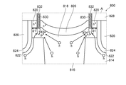
- Carriers (holes) are generated. Then, carriers (holes) generated in the p-type column region 816 move toward the source electrode side and are extracted to the source electrode through the p + -type diffusion region 834 and the metal plug 832 (see FIG. 10). .) However, when the source region 820 is also formed between the two adjacent metal plugs 832 between the two adjacent trenches 822 (see the power semiconductor device 800 according to the comparative example 2, see FIG. 10). ), Carriers (holes) generated in the p-type column region 816 move near the source region 820 formed between the two metal plugs 832 adjacent to each other.
- the semiconductor substrate 110 in which the n-type column region 114 and the p-type column region 116 form a super junction structure is provided.
- the source region 120 is formed between two trenches 122 adjacent to each other only between the trench 122 and the metal plug 132 closest to the trench. Therefore, carriers generated in the p-type column region 116 are It does not move near the source region 120, and thus carriers (holes) do not enter the source region 120. Therefore, a parasitic transistor (parasitic npn) including a source region 120 (for example, n-type), a base region 118 (for example, p-type), and an n-type column region 114 (for example, n-type) between two metal plugs 132 adjacent to each other. The transistor is not turned on.
- n-type column region 114 and the p-type column region 116 include the semiconductor substrate 110 having a super junction structure, avalanche breakdown or di / dt breakdown does not easily occur, and the breakdown resistance is large. It becomes a power semiconductor device.
- the surface of the semiconductor substrate is a recess in all of the region in which the p-type column region 116 is formed and part of the region in which the n-type column region 114 is formed in plan view. Since the particles G easily adhere to the side wall portions of the recesses, the introduction of n-type impurities by the particles G may prevent the source regions 120 from being separated (FIG. 11A). ) And (b)).
- n-type impurities are introduced by ion implantation, the ions are implanted obliquely at a shallow angle with respect to the side wall of the recess, so that the impurities are difficult to be introduced and the source region 120 may be cut off. There is.
- the metal plug 132 closest to the trench 122 is formed inside the region where the p-type column region 116 is formed in plan view, Since the source region 120 may be formed in a separated state, or a so-called disconnection may occur, there may be a problem that the source electrode 136 and the source region 120 cannot be connected.
- the metal plug 132 closest to the trench 122 between the two adjacent trenches 122 has the p-type column region 116 in plan view. Since it is formed outside the formed region, the contact portion between the source region 120 and the metal plug 132 is formed outside the side wall of the recess.
- the source region 120 is not formed in a separated state (see FIG. 11C). Even in the case of ion implantation, since the source region 120 is not formed on the sidewall of the recess, the source region 120 does not break so-called. Therefore, there is no problem that the source electrode 136 and the source region 120 cannot be connected due to this.
- the metal is tungsten, it is easy to fill the contact hole 130 with a small diameter, and the metal plug 132 with a small diameter can be formed. It can be set as the power semiconductor device made.
- the gate electrode between the region with the interlayer insulating film and the region without the interlayer insulating film (contact region).
- stress due to ultrasonic waves may concentrate on the step portion (particularly, the corner portion of the side surface of the interlayer insulating film (the boundary portion of the contact hole)), and the power semiconductor device may be destroyed.
- the metal is tungsten, and the contact hole 130 having a small diameter can be easily filled. Therefore, when the inside of the contact hole 130 is filled with tungsten, the interlayer is formed.
- the gate capacitance can be reduced.
- the amount of electric charge that the gate drive circuit (connected to the power semiconductor device 100) takes in and out of the gate electrode 126 during switching can be reduced, and drive loss can be reduced. That is, (1) at the time of turn-on, the gate drive circuit applies a positive bias to the gate electrode 126 to flow a gate current.
- the gate charge amount is obtained by multiplying the gate current amount by the energization time.
- the gate drive circuit applies a negative bias or 0 bias to the gate electrode 126 and draws out the gate current.
- the gate current amount is maintained at the same level as before and the energization time is shortened, the product of the gate current and the energization time can be reduced.
- the amount of electric charge that the drive circuit takes in and out of the gate electrode can be reduced. As a result, drive loss can be reduced.
- a large external gate resistor is inserted between the gate electrode 126 and the gate drive circuit in order to intentionally slow down the switching speed of the MOSFET and avoid ringing and noise in the circuit.
- the external gate resistor has an effect of reducing the gate current amount, and can increase the energization time and extend the switching time. Therefore, the gate charge amount that is the product of the gate current amount and the energization time remains small. As a result, drive loss can be reduced. Therefore, as described in the above (1) and (2), the amount of charge that the gate drive circuit takes in and out of the gate electrode 126 during switching can be reduced, and as a result, drive loss can be reduced.
- the power semiconductor device 100 by reducing the gate capacitance, it is possible to widen the adjustment speed of the switching speed without losing the effect of reducing the drive loss, and as a result, from the application circuit. Can answer a wide range of requests.
- the interval between the two adjacent gate electrodes 126 is not less than five times the width of the metal plug 132, and the interval between the two adjacent gate electrodes 126 is equal to Since it becomes wider with respect to the metal plug 132 and the volume of the gate electrode 126 can be made relatively small, this also makes it possible to reduce the gate capacitance. As a result, the amount of charge that the gate drive circuit takes in and out of the gate electrode 126 during switching can be reduced, and drive loss can be reduced.
- the distance between the two adjacent gate electrodes 126 is 5 times or more the width of the metal plug 132, which also reduces the gate capacitance. As a result, it is possible to widen the adjustment speed of the switching speed without losing the effect of reducing the drive loss, and as a result, it is possible to respond widely to requests from the application circuit.
- the contact hole 130 is formed to a deeper position than the bottom surface of the source region 120, the p + type diffusion formed at the bottom of the contact hole 130.
- the region 134 and the source region 120 are in contact with each other, it is possible to prevent the impurity concentration and the area of the source region 120 from being changed from the design time, and to prevent a problem that the characteristics of the power semiconductor device are changed.
- the power semiconductor device 100 since the depth of the base region 118 is in the range of 0.5 ⁇ m to 2.0 ⁇ m, it is necessary to diffuse impurities at a high temperature for a long time in the manufacturing process. There is no. Therefore, the power semiconductor device is suitable when it is difficult to diffuse impurities for a long time in order to obtain a miniaturized structure.
- the power semiconductor device 102 according to the second embodiment basically has the same configuration as that of the power semiconductor device 100 according to the first embodiment, but the number of metal plugs is different from that of the power semiconductor device 100 according to the first embodiment. Different. That is, in the power semiconductor device 102 according to the second embodiment, as shown in FIG. 12, four contact holes 130 are formed between two adjacent trenches 122, and the inside of each contact hole 130 is Is filled with metal, and four metal plugs 132 are formed.
- the source region 120 is not formed between the two adjacent metal plugs 132 between the two adjacent trenches 122. That is, between the two adjacent trenches 122, when the metal plug closest to the trench is the metal plug 132A and the other metal plug is the metal plug 132B, the metal plug 132B is not in contact with the source region 120. .
- the metal plug 132A and the metal plug 132B may have the same depth, but in the entire region where the p-type column region 116 is formed and a part of the region where the n-type column region 114 is formed in plan view. Since the recess is formed on the surface of the semiconductor substrate 110, the length of the metal plug 132B (depth of the contact hole) is longer (deeper) than the length of the metal plug 132A (depth of the contact hole). Is preferred.
- the power semiconductor device 102 according to the second embodiment is different from the power semiconductor device 100 according to the first embodiment in the number of metal plugs, but is similar to the power semiconductor device 100 according to the first embodiment. Since the contact hole 130 formed so as to penetrate at least the base region 118 through the interlayer insulating film 128 and the metal plug 132 filled with metal in the contact hole 130 is provided, the cost of the electronic device is reduced. The power semiconductor device satisfies the demands for downsizing and miniaturization and has a large breakdown resistance.
- each contact hole 130 is filled with metal. Since the metal plug 132 is formed, the depletion layer generated from the pn junction between the base region 118 and the p-type column region 116 and the n-type column region 114 is reversed between the two trenches adjacent to each other at the time of reverse bias. It can be reliably spread throughout.
- the power semiconductor device 102 according to the second embodiment has the same configuration as that of the power semiconductor device 100 according to the first embodiment except for the number of metal plugs. Therefore, the power semiconductor device 100 according to the first embodiment includes the power semiconductor device 102 according to the first embodiment. It has a corresponding effect among the effects.
- the power semiconductor device 104 according to the third embodiment basically has the same configuration as the power semiconductor device 100 according to the first embodiment, but the position of the metal plug closest to the trench is between two adjacent trenches. This is different from the case of the power semiconductor device 100 according to the first embodiment. That is, in the power semiconductor device 104 according to the third embodiment, as shown in FIG. 13, the position where the metal plug 132 closest to the trench 122 and the source region 120 are in contact with each other between the two adjacent trenches 122. , Outside the region where the p-type column region 116 is formed in plan view.
- the metal plug 132 closest to the trench 122 is formed with a region in which the n-type column region 114 is formed and a p-type column region 116 in plan view. It is formed on the boundary line with the region that has been formed.
- the power semiconductor device 104 according to the third embodiment is different from the power semiconductor device 100 according to the first embodiment in that it has a super junction structure, but the power semiconductor device 104 according to the first embodiment is different from the power semiconductor device 100 according to the first embodiment.
- a plurality of contact holes 130 formed so as to pass through the interlayer insulating film 128 and reach at least the base region 118, each formed between two adjacent trenches 122.
- the metal plug 132 filled in the contact hole 130 is provided, the power semiconductor device satisfies the demand for cost reduction and downsizing of the electronic device and has a large breakdown resistance.
- the position where the metal plug 132 closest to the trench 122 and the source region 120 are in contact with each other between the two adjacent trenches 122 is viewed in a plan view. Since the p-type column region 116 is outside the region where the p-type column region 116 is formed, the source region 120 is not formed in a separated state even with such a configuration. However, since the source region 120 is not formed on the sidewall of the recess, the source region 120 does not cause a so-called disconnection.
- the power semiconductor device 104 according to the third embodiment has the same configuration as that of the power semiconductor device 100 according to the first embodiment except that the power semiconductor device 104 has a super junction structure, and thus the power semiconductor device 100 according to the first embodiment. Has the corresponding effect among the effects of
- the metal plug 132 is formed in a stripe shape in plan view (see FIG. 14), but the present invention is not limited to this.
- the metal plug is viewed in plan, it is circular (three-dimensionally columnar, see FIGS. 15 and 19), square frame (see FIG. 16), circular frame (see FIG. 17), or lattice. (See FIG. 18) or the like.
- the trench 122 is formed in a stripe shape in plan view (see FIG. 14), but the present invention is not limited to this.
- the trench may be formed in a quadrangular shape (columnar shape, see FIGS. 18 and 19) or a lattice shape (see FIGS. 15 to 17) or the like when viewed in plan.
- the present invention is applied to the MOSFET, but the present invention is not limited to this.
- the present invention may be applied to an appropriate power semiconductor device such as an IGBT, a thyristor, a triac, or a diode.
- the contact hole 130 is formed so as to reach the base region 118, but the present invention is not limited to this.
- the contact hole 130 may be formed so as to reach the n-type column region 114 or the p-type column region 116. In this case, there is an effect that holes can be easily extracted to the source electrode 136 at the time of avalanche breakdown and reverse recovery of the body diode.
- the p + -type diffusion region 134 is formed only at the bottom of the contact hole 130, but the present invention is not limited to this.
- the p + -type diffusion region 134 may be formed in a part of the side part (a part of the side part on the bottom side) in addition to the bottom part of the contact hole 130. In this case, it is possible to prevent the power semiconductor device from being destroyed by contact of the depletion layer with the contact plug at the time of avalanche breakdown and reverse recovery of the body diode.
- two metal plugs 132 are formed between two adjacent trenches 122.
- two adjacent trenches are formed.
- four metal plugs 132 are formed between the two 122, the present invention is not limited to this.
- Three or more metal plugs 132 may be formed between two adjacent trenches 122, respectively.
- the contact hole 130 is formed up to a depth position deeper than the bottom surface of the source region 120, but the present invention is not limited to this.
- the contact hole 130 may be formed to a depth shallower than the bottom surface of the source region 120 (see the power semiconductor device 106 according to the modified example 6, FIG. 20).
- the p-type column region is formed in plan view at the position where the metal plug closest to the trench (gate electrode) and the source region are in contact with each other.
- the present invention is not limited to this.
- the position where the metal plug closest to the gate electrode contacts the source region may be outside the region where the p-type column region is formed in plan view (for example, deformation) (See power semiconductor device 200 according to Example 7, FIG. 21.)
- the source region 220 is formed only between the gate electrode 226 and the metal plug 232 closest to the gate electrode 226 between the two adjacent gate electrodes 226. Has been.
Landscapes
- Electrodes Of Semiconductors (AREA)
- Chemical & Material Sciences (AREA)
- Composite Materials (AREA)
Abstract
Description
半導体基体910は、金属プラグ932の底面に接触しており、かつ、金属プラグ932を介してソース電極936と電気的に接続され、かつ、ベース領域918よりも不純物濃度が高いp+型高濃度拡散領域934をさらに有する。
従って、平面的に見てトレンチ922とp+型高濃度拡散領域934との間隔d2が比較的長くなる(図23参照。)。よって、(1)アバランシェ降伏時及びボディダイオードの逆回復時において、(ホールが比較的発生しやすい場所である)トレンチ922の底部で発生したホールがソース電極936に引き抜かれるまでの間に比較的長い距離を移動することとなり、ベース領域918と金属プラグ932との間に高い電位差が発生しやすくなるため、ソース領域920(n型)、ベース領域918(p型)及びドリフト層914(n型)で構成される寄生npnトランジスタがオンしやすくなる(図23参照。)。また、(2)「ソース領域920とベース領域918との境界面」の面積が広くなりベース領域918のホールがソース領域920に入り込みやすくなるため、この観点においても、上記した寄生npnトランジスタがオンしやすくなる(図23参照。)。
その結果、アバランシェ破壊又はdi/dt破壊が起こりやすくなり、破壊耐量の大きなパワーMOSFETを提供することが困難となるという問題がある。なお、このような問題はパワーMOSFETの場合だけに発生し得る問題ではなく、パワー半導体装置全般に発生し得る問題である。
このような構成としたことにより、平面的に見てトレンチと第2導電型高濃度拡散領域との間隔d1が、背景技術に係るパワーMOSFET900における当該間隔d2よりも短くなる(図8参照。)。従って、(1)アバランシェ降伏時及びボディダイオードの逆回復時において、(キャリア(例えばホール)が比較的発生しやすい場所である)トレンチの底部で発生したキャリアが電極に引き抜かれるまでの間に比較的短い距離を移動することとなり、ベース領域と金属プラグとの間に高い電位差が発生し難くなるため、第1導電型高濃度拡散領域(例えばn型)、ベース領域(例えばp型)及び第1導電型コラム領域(例えばn型)で構成される寄生トランジスタ(寄生npnトランジスタ)がオンし難くなる(図8参照。)。また、(2)「第1導電型高濃度拡散領域とベース領域との境界面」の面積が狭くなりベース領域のキャリアが第1導電型高濃度拡散領域に入り込み難くなるため、この観点においても、上記した寄生トランジスタ(寄生npnトランジスタ)がオンし難くなる(図8参照。)。
その結果、アバランシェ破壊又はdi/dt破壊が起こり難くなり、破壊耐量の大きなパワー半導体装置となる。
しかしながら、第1導電型高濃度拡散領域が、互いに隣接する2つのトレンチの間において、互いに隣接する2つの金属プラグの間にも形成されている場合には、第2導電型コラム領域で発生したキャリア(ホール)が、互いに隣接する2つの金属プラグの間に形成された第1導電型高濃度拡散領域の近くを移動することとなるため、第2導電型コラム領域で発生したキャリア(ホール)が当該第1導電型高濃度拡散領域に入り込み易くなり、互いに隣接する2つの金属プラグの間の第1導電型高濃度拡散領域(例えばn型)、ベース領域(例えばp型)及び第1導電型コラム領域(例えばn型)で構成される寄生トランジスタ(寄生npnトランジスタ)がオンし易くなる。
これに対して、本発明のパワー半導体装置及びパワー半導体装置の製造方法によれば、第1導電型コラム領域及び第2導電型コラム領域でスーパージャンクション構造が構成されている半導体基体を備え、第1導電型高濃度拡散領域は、互いに隣接する2つのトレンチの間において、トレンチと当該トレンチに最も近い金属プラグとの間のみに形成されているため、第2導電型コラム領域で発生したキャリア(ホール)が、第1導電型高濃度拡散領域の近くを移動することがなく、キャリア(ホール)が第1導電型高濃度拡散領域に入り込むことがない。従って、互いに隣接する2つの金属プラグの間の第1導電型高濃度拡散領域(例えばn型)、ベース領域(例えばp型)及び第1導電型コラム領域(例えばn型)で構成される寄生トランジスタ(寄生npnトランジスタ)がオンするということもない。よって、第1導電型コラム領域及び第2導電型コラム領域でスーパージャンクション構造が構成されている半導体基体を備える場合であっても、アバランシェ破壊又はdi/dt破壊が起こり難くなり、破壊耐量の大きなパワー半導体装置となる。
1.実施形態1に係るパワー半導体装置100の構成
実施形態1に係るパワー半導体装置100は、DC-DCコンバータなど各種電源装置等に用いられるトレンチゲートパワーMOSFETである。実施形態1に係るパワー半導体装置100の耐圧は、300V以上であり、例えば600Vである。
金属プラグ132の間隔は、金属プラグ132のストライプ幅と同じ長さ又はそれ以上の長さであり、例えば0.5μm以上である。
次に、実施形態1に係るパワー半導体装置100は、以下に示す製造工程を有する製造方法(実施形態1に係るパワー半導体装置の製造方法)により製造することができる。実施形態1に係るパワー半導体装置の製造方法は、半導体基体準備工程と、トレンチ形成工程と、ゲート電極形成工程と、ベース領域形成工程と、ソース領域形成工程(第1導電型高濃度拡散領域形成工程)と、層間絶縁膜形成工程と、コンタクトホール形成工程と、p+型拡散領域形成工程(第2導電型高濃度拡散領域形成工程)と、金属プラグ充填工程と、電極形成工程とをこの順序で含む。
まず、低抵抗半導体層112と、低抵抗半導体層112上に形成され、所定の方向に沿って交互に形成された複数のn型コラム領域114及び複数のp型コラム領域116とを有し、複数のn型コラム領域114及び複数のp型コラム領域116でスーパージャンクション構造が構成されている半導体基体110を準備する。具体的には、以下のような工程を実施して半導体基体110を準備する。
まず、低抵抗半導体層112と、低抵抗半導体層112上に形成され、低抵抗半導体層112よりも不純物濃度が低いn型半導体層115(第1導電型半導体層)とが積層された半導体基体110を準備する(図2(a)参照。)。半導体基体110としては、適宜の半導体基体を用いることができるが、例えばn+型の低抵抗半導体層112上にエピタキシャル成長法によってn-型のn型半導体層115を形成してなる半導体基体を用いることができる。
次に、n型半導体層115の表面に所定の方向に沿って配列されるように、絶縁膜M1をマスクとするエッチングによって所定の深さの複数のp型コラム用トレンチ117(第2導電型コラム用トレンチ)を形成する(図2(b)参照。)。絶縁膜M1の厚さは適宜の厚さとすることができる。n型半導体層115において、p型コラム用トレンチ117の深さ位置から、低抵抗半導体層112とn型半導体層115との間の境界面の深さ位置までの間はバッファ層113となる。
次に、p型コラム用トレンチ117の内部に、絶縁膜M1の表面高さを超える高さ位置までp型半導体材料(第2導電型半導体材料)をエピタキシャル成長させることによってp型埋込層116’(第2導電型埋込層)を形成する(図2(c)参照。)。
次に、p型埋込層116’における絶縁膜M1の表面高さを超える部分をCMP法によって除去する(図2(d)参照。)。
次に、p型埋込層116’の表面を絶縁膜M1の底面の深さ位置よりも深くなるようにエッチングする(図3(a)参照。)。エッチングの方法は、等方性エッチングでもよいし異方性エッチングでもよい(実施形態1においては、等方性エッチング。)。このようにしてp型コラム用トレンチ117内に充填されたp型埋込層116’がp型コラム領域116となる。
次に、n型コラム領域114が形成されている領域内に複数のトレンチ122を形成する。具体的には、トレンチ122に対応する開口を有するマスク(図示せず。)をn型コラム領域114の一部及びp型コラム領域116の全部の表面上に形成し、当該マスクを用いてエッチングを行うことにより、複数のトレンチ122を形成する(図3(c)参照。)。次に、エッチング後、マスクを除去し、犠牲酸化によりトレンチ122の表面を整える。
次に、トレンチ122の内周面を含む半導体基体110の表面上に熱酸化により熱酸化膜124’を形成する(図3(d)参照。)。このとき、トレンチ122の内周面の熱酸化膜がゲート絶縁膜124となる。その後、当該熱酸化膜124’上にポリシリコン126’を堆積させる。次に、当該ポリシリコン126’全面にn型不純物(例えば、リン)をイオン注入し(図4(a)参照。)、熱拡散させる。次に、トレンチ122の内部を除いてポリシリコンを除去する。これにより、トレンチ122の内部にゲート絶縁膜124を介してゲート電極126を形成する(図4(b)参照。)。
次に、半導体基体110の表面に熱酸化膜124’を介してp型不純物(例えばボロン)をイオン注入する(図4(c)参照。)。次に、当該p型不純物を熱拡散させて半導体基体110の表面からトレンチ122の最底部よりも浅い深さ位置までベース領域118を形成する(図5(a)参照。)。
次に、ソース領域120、ゲート絶縁膜124及びゲート電極126に対応する開口を有するマスクM2を熱酸化膜124’上に形成し、当該マスクM2を介してn型不純物(例えばヒ素)をイオン注入する(図5(b)参照。)。次に、マスクM2を除去する。次に、当該n型不純物を熱拡散することにより、ベース領域118の表面のうちの所定の領域に、一部がトレンチ122の内周面に露出するようにソース領域120を形成する(図5(c)参照。)。
次に、ベース領域118、ソース領域120、ゲート絶縁膜124及びゲート電極126を覆う層間絶縁膜128を形成する(図6(a)参照。)。具体的には、熱酸化膜124’及びゲート電極126上にCVD法によりPSG膜を形成する。これにより、熱酸化膜124’及びPSG膜で構成された層間絶縁膜128を形成する。
次に、互いに隣接する2つのトレンチ122間にそれぞれ2つずつコンタクトホール130に対応する開口を有するマスク(図示せず。)を層間絶縁膜128の表面に形成する。コンタクトホール形成工程においては、互いに隣接する2つのトレンチ122の間において、ソース領域120がトレンチ122と当該トレンチに最も近い金属プラグ132との間のみに形成された状態となるように、トレンチ122に最も近いコンタクトホール130を形成する。言い換えると、トレンチ122に最も近いコンタクトホール130を、トレンチ122側の側壁がソース領域120と接触し、かつ、トレンチ122側とは反対側の側壁がベース領域118と接触する位置に形成する。次に、当該マスクを用いて層間絶縁膜128を貫通してベース領域118に達するようにエッチングを行うことによりコンタクトホール130を形成する。エッチング後、マスクを除去する(図6(b)参照。)。
次に、コンタクトホール130の底面に、ベース領域118よりも高い不純物濃度でp型不純物(例えばボロン)をイオン注入する(図6(c)参照。)。次に、当該p型不純物を熱拡散しすることにより、コンタクトホール130の底面に接触してなるp+型拡散領域134を形成する(図7(a)参照。)。
次に、スパッタ法によりコンタクトホール130の内側面にバリアメタル(図示せず。)を成膜し、当該バリアメタルをアニールする。次にCVD法により当該バリアメタル上にタングステンを成膜することにより、コンタクトホール130の内部に当該バリアメタルを介してタングステンを充填する。次に、CMP法によって層間絶縁膜128上のタングステンを除去することにより、コンタクトホール130の内部にのみタングステンを残し、金属プラグ132を形成する(図7(b)参照。)。なお、バリアメタルの組成としては、チタンナイトライド(TiN)、チタンタングステン(TiW)、モリブデンシリコン(MоSi)等を用いることができる。
次に、スパッタ法により層間絶縁膜128及び金属プラグ132上にAl-Cu系金属を成膜し、金属プラグ132を介してベース領域118、ソース領域120及びp+型拡散領域134と電気的に接続するソース電極136を形成する。また、低抵抗半導体層112上にTi-Ni-Auなどの多層金属膜を成膜し、ドレイン電極138を形成する(図7(c)参照。)。
実施形態1に係るパワー半導体装置100及びパワー半導体装置の製造方法によれば、層間絶縁膜128を貫通して少なくともベース領域118に達するように形成されたコンタクトホール130と、コンタクトホール130の内部に金属が充填されてなる金属プラグ132とを備えるため、背景技術に係るパワーMOSFET900の場合と同様に、ソース電極136がソース領域120と直接コンタクトしているパワー半導体装置の場合のように径が大きいコンタクトホールを形成しなくても済み、微細化されたパワー半導体装置とすることができる。その結果、実施形態1に係るパワー半導体装置100及びパワー半導体装置の製造方法は、電子機器の低コスト化及び小型化の要請に適うパワー半導体装置及びパワー半導体装置の製造方法とすることができる。
このような構成としたことにより、平面的に見てトレンチ122とp+型拡散領域134との間隔d1(図8参照。)が、背景技術に係るパワーMOSFET900における当該間隔d2(図23参照。)よりも短くなる。従って、(1)アバランシェ降伏時及びボディダイオードの逆回復時において、(ホールが比較的発生しやすい場所である)トレンチ122の底部で発生したホールがソース電極136に引き抜かれるまでの間に比較的短い距離を移動することとなり、ベース領域118と金属プラグ132との間に高い電位差が発生し難くなるため、ソース領域120(n型)、ベース領域118(p型)及びn型コラム領域114(n型)で構成される寄生npnトランジスタがオンし難くなる(図8参照。)。また、(2)「ソース領域120とベース領域118との境界面」の面積が狭くなりベース領域118のホールがソース領域120に入り込み難くなるため、この観点においても、上記した寄生npnトランジスタがオンし難くなる(図8参照。)。
その結果、実施形態1に係るパワー半導体装置100及びパワー半導体装置の製造方法は、アバランシェ破壊又はdi/dt破壊が起こり難くなり、破壊耐量の大きなパワー半導体装置及びパワー半導体装置の製造方法とすることができる。
しかしながら、ソース領域820が、互いに隣接する2つのトレンチ822の間において、互いに隣接する2つの金属プラグ832の間にも形成されている場合(比較例2に係るパワー半導体装置800、図10参照。)には、p型コラム領域816で発生したキャリア(ホール)が、互いに隣接する2つの金属プラグ832の間に形成されたソース領域820の近くを移動することとなる。従って、互いに隣接する2つの金属プラグ832の間において、キャリア(ホール)がソース領域820に入り込み易くなり、互いに隣接する2つの金属プラグ832の間のソース領域820(例えばn型)、ベース領域818(例えばp型)及びn型コラム領域814(例えばn型)で構成される寄生トランジスタ(寄生npnトランジスタ)がオンし易くなる。
これに対して、実施形態1に係るパワー半導体装置100及びパワー半導体装置の製造方法によれば、n型コラム領域114及びp型コラム領域116でスーパージャンクション構造が構成されている半導体基体110を備え、ソース領域120は、互いに隣接する2つのトレンチ122の間において、トレンチ122と当該トレンチに最も近い金属プラグ132との間のみに形成されているため、p型コラム領域116で発生したキャリアが、ソース領域120の近くを移動することがなく、従って、キャリア(ホール)がソース領域120に入り込むことがない。従って、互いに隣接する2つの金属プラグ132の間のソース領域120(例えばn型)、ベース領域118(例えばp型)及びn型コラム領域114(例えばn型)で構成される寄生トランジスタ(寄生npnトランジスタ)がオンするということもない。この結果、n型コラム領域114及びp型コラム領域116でスーパージャンクション構造が構成されている半導体基体110を備える場合であっても、アバランシェ破壊又はdi/dt破壊が起こり難くなり、破壊耐量の大きなパワー半導体装置となる。
従って、互いに隣接する2つのトレンチ122の間において、トレンチ122に最も近い金属プラグ132が、平面的に見てp型コラム領域116が形成されている領域の内側に形成されている場合には、ソース領域120が分離した状態で形成されたり、いわゆる段切れを起こしたりすることがあるため、ソース電極136とソース領域120とが接続できない不具合が生じるおそれがある。
これに対して、実施形態1に係るパワー半導体装置100によれば、互いに隣接する2つのトレンチ122の間において、トレンチ122に最も近い金属プラグ132は、平面的に見てp型コラム領域116が形成されている領域の外側に形成されているため、ソース領域120と金属プラグ132との接触部分が凹部の側壁よりも外側に形成されることとなる。従って、凹部の側壁の部分にはパーティクルGが付着したとしても、ソース領域120が分離した状態で形成される、ということがない(図11(c)参照。)。また、イオン注入する場合でも、凹部の側壁にソース領域120を形成することがないため、ソース領域120がいわゆる段切れを起こすこともない。従って、このことを原因とした、ソース電極136とソース領域120とが接続できない不具合が生じない。
すなわち、(1)ターンオンの際には、ゲートドライブ回路は、ゲート電極126に対しプラスバイアスを与え、ゲート電流を流し込む。ゲート電流量に通電時間を掛け算すると、ゲート電荷量となる。ゲート容量が小さくなるとゲート電荷量が減るため、ゲート電流量と通電時間の積が小さくて済むことになる。その結果、ゲート電流量を減らすか、通電時間を短くするか、いずれかが可能となり、結果的に、ドライブ回路側の電力損失を低減することができる。
また、(2)ターンオフの際は、ゲートドライブ回路は、ゲート電極126に対しマイナスバイアスまたは0バイアスを与え、ゲート電流を引き抜く。このとき、(a)ゲート電荷量が少なくなったとき、ゲート電流量を以前と同等に維持して、通電時間を短くした場合には、ゲート電流と通電時間の積が小さくて済むため、ゲートドライブ回路がゲート電極に対して出し入れする電荷量を減らすことができる。その結果、ドライブ損失を低減することができる。また、(b)MOSFETのスイッチング速度を意図的に遅くし、回路にリンギングやノイズが発生するのを避けるために、ゲート電極126とゲートドライブ回路との間に大きめの外付けゲート抵抗を挿入した場合でも、当該外付けゲート抵抗は、ゲート電流量を絞る効果があり、通電時間を長くし、スイッチング時間を引き延ばすことができることから、ゲート電流量と通電時間の積であるゲート電荷量は小さいままであり、その結果、ドライブ損失を低減することができる。
従って、上記(1)及び(2)で記載したように、スイッチングの際、ゲートドライブ回路がゲート電極126に対して出し入れする電荷量を減らすことができ、その結果、ドライブ損失を低減できる。
また、上記(2)(b)の場合のように、MOSFETのスイッチング速度を意図的に遅くし、回路にリンギングやノイズが発生するのを避けるために、ゲート電極126とゲートドライブ回路との間に大きめの外付けゲート抵抗を挿入した場合であっても、外付けゲート抵抗は、ゲート電流量を絞る効果があり、通電時間を長くし、スイッチング時間を引き延ばすことができる。その結果、スイッチング速度が遅くなり、スイッチング時間が長くなることから、dv/dtが緩慢になり、回路にリンギングやノイズが発生するのを避けることができる。
従って、実施形態1に係るパワー半導体装置100によれば、ゲート容量が減ることによって、ドライブ損失を低減する効果を失うことなくスイッチング速度の調整しろを広くすることができ、その結果、アプリケーション回路からの要請に幅広く答えることができる。
実施形態2に係るパワー半導体装置102は、基本的には実施形態1に係るパワー半導体装置100と同様の構成を有するが、金属プラグの本数が実施形態1に係るパワー半導体装置100の場合とは異なる。すなわち、実施形態2に係るパワー半導体装置102においては、図12に示すように、コンタクトホール130が、互いに隣接する2つのトレンチ122の間にそれぞれ4本形成されており、各コンタクトホール130の内部には金属が充填されており、金属プラグ132が4本形成されている。
実施形態3に係るパワー半導体装置104は、基本的には実施形態1に係るパワー半導体装置100と同様の構成を有するが、互いに隣接する2つのトレンチの間においてトレンチに最も近い金属プラグの位置が実施形態1に係るパワー半導体装置100の場合とは異なる。すなわち、実施形態3に係るパワー半導体装置104においては、図13に示すように、互いに隣接する2つのトレンチ122の間において、トレンチ122に最も近い金属プラグ132とソース領域120とが接触する位置は、平面的に見てp型コラム領域116が形成されている領域の外側である。
Claims (10)
- 低抵抗半導体層と、前記低抵抗半導体層上に形成され、所定の方向に沿って交互に形成された複数の第1導電型コラム領域及び複数の第2導電型コラム領域と、前記複数の第1導電型コラム領域及び前記複数の第2導電型コラム領域の表面上に形成された第2導電型のベース領域と、前記ベース領域の表面のうちの所定の位置に形成された第1導電型高濃度拡散領域とを有し、前記複数の第1導電型コラム領域及び前記複数の第2導電型コラム領域でスーパージャンクション構造が構成されている半導体基体と、
平面的に見て前記第1導電型コラム領域が形成されている領域内に、前記ベース領域を貫通し前記第1導電型コラム領域に達する深さ位置まで形成され、かつ、前記第1導電型高濃度拡散領域の一部が内周面に露出するように形成された複数のトレンチと、
前記トレンチの内周面に形成されたゲート絶縁膜と、
前記ゲート絶縁膜を介して前記トレンチの内部に埋め込まれてなるゲート電極と、
前記ベース領域、前記第1導電型高濃度拡散領域、前記ゲート絶縁膜及び前記ゲート電極を覆う層間絶縁膜と、
互いに隣接する2つの前記トレンチの間にそれぞれ2本以上、前記層間絶縁膜を貫通して少なくとも前記ベース領域に達するように形成されたコンタクトホールと、
前記コンタクトホールの内部に金属が充填されてなる金属プラグと、
前記層間絶縁膜上に形成され、前記金属プラグを介して前記ベース領域及び前記第1導電型高濃度拡散領域と電気的に接続された電極とを備え、
前記半導体基体は、前記金属プラグの底面に接触しており、かつ、前記金属プラグを介して前記電極と電気的に接続され、かつ、前記ベース領域よりも不純物濃度が高い第2導電型高濃度拡散領域をさらに有し、
前記半導体基体において、前記第1導電型高濃度拡散領域は、互いに隣接する2つの前記トレンチの間において、前記トレンチと当該トレンチに最も近い前記金属プラグとの間のみに形成されていることを特徴とするパワー半導体装置。 - 互いに隣接する2つの前記トレンチの間において、前記トレンチに最も近い前記金属プラグと前記第1導電型高濃度拡散領域とが接触する位置は、平面的に見て前記第2導電型コラム領域が形成されている領域の外側であることを特徴とする請求項1に記載のパワー半導体装置。
- 互いに隣接する2つの前記トレンチの間において、前記トレンチに最も近い前記金属プラグは、平面的に見て前記第2導電型コラム領域が形成されている領域の外側に形成されていることを特徴とする請求項1に記載のパワー半導体装置。
- 前記金属は、タングステンであることを特徴とする請求項1~3のいずれかに記載のパワー半導体装置。
- 互いに隣接する2つの前記ゲート電極の間隔は、2.5μm以上であることを特徴とする請求項1~4のいずれかに記載のパワー半導体装置。
- 互いに隣接する2つの前記ゲート電極の間隔は、前記金属プラグの幅の5倍以上であることを特徴とする請求項1~5のいずれかに記載のパワー半導体装置。
- 前記コンタクトホールは、前記第1導電型高濃度拡散領域の底面よりも深い深さ位置まで形成されていることを特徴とする請求項1~6のいずれかに記載のパワー半導体装置。
- 前記ベース領域の最深部の深さ位置は、0.5μm~2.0μmの範囲内にあることを特徴とする請求項1~7のいずれかに記載のパワー半導体装置。
- 請求項1~8のいずれかに記載のパワー半導体装置を製造するためのパワー半導体装置の製造方法であって、
低抵抗半導体層と、前記低抵抗半導体層上に形成され、所定の方向に沿って交互に形成された複数の第1導電型コラム領域及び複数の第2導電型コラム領域とを有し、前記複数の第1導電型コラム領域及び前記複数の第2導電型コラム領域でスーパージャンクション構造が構成されている半導体基体を準備する半導体基体準備工程と、
前記第1導電型コラム領域が形成されている領域内に複数のトレンチを形成するトレンチ形成工程と、
前記トレンチの内周面にゲート絶縁膜を形成した後、前記ゲート絶縁膜を介して前記トレンチの内部にゲート電極を形成するゲート電極形成工程と、
前記複数の第1導電型コラム領域及び前記複数の第2導電型コラム領域の表面から前記トレンチの最底部よりも浅い深さ位置まで第2導電型のベース領域を形成するベース領域形成工程と、
前記ベース領域の表面のうちの所定の領域に、少なくとも一部が前記トレンチの内周面に露出するように第1導電型高濃度拡散領域を形成する第1導電型高濃度拡散領域形成工程と、
前記ベース領域、前記第1導電型高濃度拡散領域、前記ゲート絶縁膜及び前記ゲート電極を覆う層間絶縁膜を形成する層間絶縁膜形成工程と、
互いに隣接する2つの前記トレンチ間にそれぞれ2本以上、前記層間絶縁膜を貫通して少なくとも前記ベース領域に達する前記コンタクトホールを形成するコンタクトホール形成工程と、
前記コンタクトホールの底面に接触してなる、前記ベース領域よりも不純物濃度が高い第2導電型高濃度拡散領域を形成する第2導電型高濃度拡散領域形成工程と、
前記コンタクトホールの内部に金属を充填することによって金属プラグを形成する金属プラグ形成工程と、
前記層間絶縁膜上に、前記金属プラグを介して前記ベース領域、前記第1導電型高濃度拡散領域及び前記第2導電型高濃度拡散領域と電気的に接続された電極を形成する電極形成工程とをこの順序で含み、
前記コンタクトホール形成工程においては、互いに隣接する2つの前記トレンチの間において、前記第1導電型高濃度拡散領域が前記トレンチと当該トレンチに最も近い前記金属プラグとの間のみに形成された状態となるように、前記トレンチに最も近い前記コンタクトホールを形成することを特徴とするパワー半導体装置の製造方法。 - 前記半導体基体準備工程は、
低抵抗半導体層と、前記低抵抗半導体層上に形成され、前記低抵抗半導体層よりも不純物濃度が低い第1導電型半導体層とが積層された半導体基体を準備する第1工程と、
前記第1導電型半導体層の表面に所定の方向に沿って配列した状態となるように、絶縁膜をマスクとするエッチングによって所定の深さの複数の第2導電型コラム用トレンチを形成する第2工程と、
前記第2導電型コラム用トレンチの内部に、前記絶縁膜の表面高さを超える高さ位置まで第2導電型半導体材料をエピタキシャル成長させることによって第2導電型埋込層を形成する第3工程と、
前記第2導電型埋込層における前記絶縁膜の表面高さを超える部分を除去する第4工程と、
前記第2導電型埋込層の表面を前記絶縁膜の底面の深さ位置よりも深くなるようにエッチングして第2導電型コラム領域を形成する第5工程とをこの順序で含むことを特徴とする請求項9に記載のパワー半導体装置の製造方法。
Priority Applications (5)
| Application Number | Priority Date | Filing Date | Title |
|---|---|---|---|
| US15/760,458 US10468518B2 (en) | 2016-01-29 | 2017-01-16 | Power semiconductor device having a first and a second conductive-type columnar regions formed alternately with each other and method of manufacturing the power semiconductor device |
| JP2017564175A JP6832296B2 (ja) | 2016-01-29 | 2017-01-16 | パワー半導体装置及びパワー半導体装置の製造方法 |
| CN201780008005.0A CN108496252B (zh) | 2016-01-29 | 2017-01-16 | 功率半导体装置以及功率半导体装置的制造方法 |
| TW106103075A TWI655769B (zh) | 2016-01-29 | 2017-01-25 | 功率半導體裝置及其製造方法 |
| NL2018242A NL2018242B1 (en) | 2016-01-29 | 2017-01-27 | Power semiconductor device and method of manufacturing power semiconductor device |
Applications Claiming Priority (2)
| Application Number | Priority Date | Filing Date | Title |
|---|---|---|---|
| JPPCT/JP2016/052631 | 2016-01-29 | ||
| PCT/JP2016/052631 WO2017130374A1 (ja) | 2016-01-29 | 2016-01-29 | パワー半導体装置及びパワー半導体装置の製造方法 |
Publications (1)
| Publication Number | Publication Date |
|---|---|
| WO2017130778A1 true WO2017130778A1 (ja) | 2017-08-03 |
Family
ID=58779327
Family Applications (2)
| Application Number | Title | Priority Date | Filing Date |
|---|---|---|---|
| PCT/JP2016/052631 Ceased WO2017130374A1 (ja) | 2016-01-29 | 2016-01-29 | パワー半導体装置及びパワー半導体装置の製造方法 |
| PCT/JP2017/001288 Ceased WO2017130778A1 (ja) | 2016-01-29 | 2017-01-16 | パワー半導体装置及びパワー半導体装置の製造方法 |
Family Applications Before (1)
| Application Number | Title | Priority Date | Filing Date |
|---|---|---|---|
| PCT/JP2016/052631 Ceased WO2017130374A1 (ja) | 2016-01-29 | 2016-01-29 | パワー半導体装置及びパワー半導体装置の製造方法 |
Country Status (6)
| Country | Link |
|---|---|
| US (1) | US10468518B2 (ja) |
| JP (1) | JP6832296B2 (ja) |
| CN (1) | CN108496252B (ja) |
| NL (1) | NL2018242B1 (ja) |
| TW (1) | TWI655769B (ja) |
| WO (2) | WO2017130374A1 (ja) |
Families Citing this family (11)
| Publication number | Priority date | Publication date | Assignee | Title |
|---|---|---|---|---|
| JP7051641B2 (ja) * | 2018-08-24 | 2022-04-11 | ルネサスエレクトロニクス株式会社 | 半導体装置およびその製造方法 |
| CN109860301B (zh) * | 2019-01-21 | 2020-06-30 | 东南大学 | 一种低反向恢复电荷sj-vdmos器件 |
| CN109887990A (zh) * | 2019-01-30 | 2019-06-14 | 上海华虹宏力半导体制造有限公司 | 超结igbt器件及其制造方法 |
| EP3748685A1 (en) * | 2019-06-06 | 2020-12-09 | Infineon Technologies Dresden GmbH & Co . KG | Semiconductor device |
| CN111370482A (zh) * | 2020-04-27 | 2020-07-03 | 上海华虹宏力半导体制造有限公司 | Igbt器件及igbt器件的制备方法 |
| CN114496987B (zh) * | 2022-04-18 | 2022-08-02 | 绍兴中芯集成电路制造股份有限公司 | Mosfet功率器件及其形成方法、csp封装模块 |
| CN115911093B (zh) * | 2022-11-11 | 2026-01-23 | 天狼芯半导体(成都)有限公司 | 碳化硅mosfet的结构、制造方法及电子设备 |
| JP7818027B2 (ja) * | 2024-03-04 | 2026-02-19 | 株式会社東芝 | 半導体装置 |
| TWI871247B (zh) * | 2024-06-20 | 2025-01-21 | 李羿軒 | 垂直型超接面功率半導體裝置 |
| TWI871248B (zh) * | 2024-06-20 | 2025-01-21 | 李羿軒 | 垂直型超接面功率半導體裝置 |
| TWI871246B (zh) * | 2024-06-20 | 2025-01-21 | 李羿軒 | 垂直型超接面功率半導體裝置 |
Citations (6)
| Publication number | Priority date | Publication date | Assignee | Title |
|---|---|---|---|---|
| JP2006294853A (ja) * | 2005-04-11 | 2006-10-26 | Nec Electronics Corp | 電界効果トランジスタ |
| JP2008153620A (ja) * | 2006-11-21 | 2008-07-03 | Toshiba Corp | 半導体装置 |
| US20140103426A1 (en) * | 2012-10-12 | 2014-04-17 | Fu-Yuan Hsieh | Trench metal oxide semiconductor field effect transistor with multiple trenched source-body contacts for reducing gate charge |
| US20150155380A1 (en) * | 2013-12-04 | 2015-06-04 | Infineon Technologies Austria Ag | Manufacturing a Semiconductor Device Using Electrochemical Etching, Semiconductor Device and Super Junction Semiconductor Device |
| JP2015185646A (ja) * | 2014-03-24 | 2015-10-22 | ルネサスエレクトロニクス株式会社 | 半導体装置 |
| JP2016163004A (ja) * | 2015-03-05 | 2016-09-05 | 株式会社東芝 | 半導体装置および半導体装置の製造方法 |
Family Cites Families (13)
| Publication number | Priority date | Publication date | Assignee | Title |
|---|---|---|---|---|
| JPH06252090A (ja) | 1993-02-22 | 1994-09-09 | Nippon Steel Corp | 半導体装置及びその製造方法 |
| JP2007149867A (ja) * | 2005-11-25 | 2007-06-14 | Toyota Industries Corp | 半導体装置 |
| JP5135759B2 (ja) * | 2006-10-19 | 2013-02-06 | 富士電機株式会社 | 超接合半導体装置の製造方法 |
| US20080116512A1 (en) | 2006-11-21 | 2008-05-22 | Kabushiki Kaisha Toshiba | Semiconductor device and method of making the same |
| JP4670915B2 (ja) * | 2008-08-08 | 2011-04-13 | ソニー株式会社 | 半導体装置 |
| US7960787B2 (en) * | 2008-11-07 | 2011-06-14 | Force-Mos Technology Corporation | Configuration of trenched semiconductor power device to reduce masked process |
| JP5625291B2 (ja) * | 2009-09-11 | 2014-11-19 | 富士電機株式会社 | 半導体装置およびその製造方法 |
| TWI430432B (zh) * | 2011-01-27 | 2014-03-11 | Sinopower Semiconductor Inc | 具有防靜電結構之功率半導體元件及其製作方法 |
| US8421149B2 (en) * | 2011-05-25 | 2013-04-16 | Great Power Semiconductor Corp. | Trench power MOSFET structure with high switching speed and fabrication method thereof |
| JP6047297B2 (ja) * | 2012-04-09 | 2016-12-21 | ルネサスエレクトロニクス株式会社 | 半導体装置 |
| US8860130B2 (en) * | 2012-11-05 | 2014-10-14 | Alpha And Omega Semiconductor Incorporated | Charged balanced devices with shielded gate trench |
| US9853140B2 (en) | 2012-12-31 | 2017-12-26 | Vishay-Siliconix | Adaptive charge balanced MOSFET techniques |
| US9099320B2 (en) * | 2013-09-19 | 2015-08-04 | Force Mos Technology Co., Ltd. | Super-junction structures having implanted regions surrounding an N epitaxial layer in deep trench |
-
2016
- 2016-01-29 WO PCT/JP2016/052631 patent/WO2017130374A1/ja not_active Ceased
-
2017
- 2017-01-16 CN CN201780008005.0A patent/CN108496252B/zh active Active
- 2017-01-16 US US15/760,458 patent/US10468518B2/en active Active
- 2017-01-16 JP JP2017564175A patent/JP6832296B2/ja active Active
- 2017-01-16 WO PCT/JP2017/001288 patent/WO2017130778A1/ja not_active Ceased
- 2017-01-25 TW TW106103075A patent/TWI655769B/zh active
- 2017-01-27 NL NL2018242A patent/NL2018242B1/en active
Patent Citations (6)
| Publication number | Priority date | Publication date | Assignee | Title |
|---|---|---|---|---|
| JP2006294853A (ja) * | 2005-04-11 | 2006-10-26 | Nec Electronics Corp | 電界効果トランジスタ |
| JP2008153620A (ja) * | 2006-11-21 | 2008-07-03 | Toshiba Corp | 半導体装置 |
| US20140103426A1 (en) * | 2012-10-12 | 2014-04-17 | Fu-Yuan Hsieh | Trench metal oxide semiconductor field effect transistor with multiple trenched source-body contacts for reducing gate charge |
| US20150155380A1 (en) * | 2013-12-04 | 2015-06-04 | Infineon Technologies Austria Ag | Manufacturing a Semiconductor Device Using Electrochemical Etching, Semiconductor Device and Super Junction Semiconductor Device |
| JP2015185646A (ja) * | 2014-03-24 | 2015-10-22 | ルネサスエレクトロニクス株式会社 | 半導体装置 |
| JP2016163004A (ja) * | 2015-03-05 | 2016-09-05 | 株式会社東芝 | 半導体装置および半導体装置の製造方法 |
Also Published As
| Publication number | Publication date |
|---|---|
| TWI655769B (zh) | 2019-04-01 |
| US10468518B2 (en) | 2019-11-05 |
| NL2018242A (en) | 2017-08-02 |
| JP6832296B2 (ja) | 2021-02-24 |
| WO2017130374A1 (ja) | 2017-08-03 |
| JPWO2017130778A1 (ja) | 2018-11-22 |
| NL2018242B1 (en) | 2017-12-12 |
| CN108496252B (zh) | 2021-05-25 |
| TW201806147A (zh) | 2018-02-16 |
| US20180269318A1 (en) | 2018-09-20 |
| CN108496252A (zh) | 2018-09-04 |
Similar Documents
| Publication | Publication Date | Title |
|---|---|---|
| CN108496252B (zh) | 功率半导体装置以及功率半导体装置的制造方法 | |
| JP6817443B2 (ja) | ゲート・トレンチと、埋め込まれた終端構造とを有するパワー半導体デバイス、及び、関連方法 | |
| JP5530602B2 (ja) | 半導体装置およびその製造方法 | |
| JP6101183B2 (ja) | 半導体装置 | |
| JP2009141243A (ja) | 半導体装置 | |
| JP6418538B2 (ja) | 半導体装置及び半導体装置の製造方法 | |
| JP6164372B2 (ja) | 半導体装置および半導体装置の製造方法 | |
| CN106469751A (zh) | 半导体器件及其制作方法 | |
| JP6154083B1 (ja) | パワー半導体装置及びパワー半導体装置の製造方法 | |
| JP2008235590A (ja) | 半導体装置 | |
| CN108305893B (zh) | 半导体装置 | |
| US9059237B2 (en) | Semiconductor device having an insulated gate bipolar transistor | |
| CN100477263C (zh) | 超级结半导体元件及其制造方法 | |
| JP2002026314A (ja) | 半導体装置 | |
| CN112889158B (zh) | 半导体装置 | |
| WO2017149624A1 (ja) | パワー半導体装置及びパワー半導体装置の製造方法 | |
| JP5922379B2 (ja) | モノリシック集積回路の製造方法 | |
| CN118591887A (zh) | 半导体装置及半导体装置的制造方法 |
Legal Events
| Date | Code | Title | Description |
|---|---|---|---|
| 121 | Ep: the epo has been informed by wipo that ep was designated in this application |
Ref document number: 17744009 Country of ref document: EP Kind code of ref document: A1 |
|
| WWE | Wipo information: entry into national phase |
Ref document number: 15760458 Country of ref document: US |
|
| WWE | Wipo information: entry into national phase |
Ref document number: 2017564175 Country of ref document: JP |
|
| NENP | Non-entry into the national phase |
Ref country code: DE |
|
| 122 | Ep: pct application non-entry in european phase |
Ref document number: 17744009 Country of ref document: EP Kind code of ref document: A1 |