WO2017126207A1 - 半導体装置の製造方法 - Google Patents
半導体装置の製造方法 Download PDFInfo
- Publication number
- WO2017126207A1 WO2017126207A1 PCT/JP2016/084092 JP2016084092W WO2017126207A1 WO 2017126207 A1 WO2017126207 A1 WO 2017126207A1 JP 2016084092 W JP2016084092 W JP 2016084092W WO 2017126207 A1 WO2017126207 A1 WO 2017126207A1
- Authority
- WO
- WIPO (PCT)
- Prior art keywords
- film
- electrode
- forming
- layer
- capacitor
- Prior art date
- Legal status (The legal status is an assumption and is not a legal conclusion. Google has not performed a legal analysis and makes no representation as to the accuracy of the status listed.)
- Ceased
Links
Images


Classifications
-
- H—ELECTRICITY
- H10—SEMICONDUCTOR DEVICES; ELECTRIC SOLID-STATE DEVICES NOT OTHERWISE PROVIDED FOR
- H10D—INORGANIC ELECTRIC SEMICONDUCTOR DEVICES
- H10D1/00—Resistors, capacitors or inductors
- H10D1/60—Capacitors
- H10D1/68—Capacitors having no potential barriers
- H10D1/692—Electrodes
- H10D1/696—Electrodes comprising multiple layers, e.g. comprising a barrier layer and a metal layer
-
- C—CHEMISTRY; METALLURGY
- C23—COATING METALLIC MATERIAL; COATING MATERIAL WITH METALLIC MATERIAL; CHEMICAL SURFACE TREATMENT; DIFFUSION TREATMENT OF METALLIC MATERIAL; COATING BY VACUUM EVAPORATION, BY SPUTTERING, BY ION IMPLANTATION OR BY CHEMICAL VAPOUR DEPOSITION, IN GENERAL; INHIBITING CORROSION OF METALLIC MATERIAL OR INCRUSTATION IN GENERAL
- C23C—COATING METALLIC MATERIAL; COATING MATERIAL WITH METALLIC MATERIAL; SURFACE TREATMENT OF METALLIC MATERIAL BY DIFFUSION INTO THE SURFACE, BY CHEMICAL CONVERSION OR SUBSTITUTION; COATING BY VACUUM EVAPORATION, BY SPUTTERING, BY ION IMPLANTATION OR BY CHEMICAL VAPOUR DEPOSITION, IN GENERAL
- C23C14/00—Coating by vacuum evaporation, by sputtering or by ion implantation of the coating forming material
- C23C14/06—Coating by vacuum evaporation, by sputtering or by ion implantation of the coating forming material characterised by the coating material
-
- C—CHEMISTRY; METALLURGY
- C23—COATING METALLIC MATERIAL; COATING MATERIAL WITH METALLIC MATERIAL; CHEMICAL SURFACE TREATMENT; DIFFUSION TREATMENT OF METALLIC MATERIAL; COATING BY VACUUM EVAPORATION, BY SPUTTERING, BY ION IMPLANTATION OR BY CHEMICAL VAPOUR DEPOSITION, IN GENERAL; INHIBITING CORROSION OF METALLIC MATERIAL OR INCRUSTATION IN GENERAL
- C23C—COATING METALLIC MATERIAL; COATING MATERIAL WITH METALLIC MATERIAL; SURFACE TREATMENT OF METALLIC MATERIAL BY DIFFUSION INTO THE SURFACE, BY CHEMICAL CONVERSION OR SUBSTITUTION; COATING BY VACUUM EVAPORATION, BY SPUTTERING, BY ION IMPLANTATION OR BY CHEMICAL VAPOUR DEPOSITION, IN GENERAL
- C23C16/00—Chemical coating by decomposition of gaseous compounds, without leaving reaction products of surface material in the coating, i.e. chemical vapour deposition [CVD] processes
- C23C16/06—Chemical coating by decomposition of gaseous compounds, without leaving reaction products of surface material in the coating, i.e. chemical vapour deposition [CVD] processes characterised by the deposition of metallic material
-
- C—CHEMISTRY; METALLURGY
- C23—COATING METALLIC MATERIAL; COATING MATERIAL WITH METALLIC MATERIAL; CHEMICAL SURFACE TREATMENT; DIFFUSION TREATMENT OF METALLIC MATERIAL; COATING BY VACUUM EVAPORATION, BY SPUTTERING, BY ION IMPLANTATION OR BY CHEMICAL VAPOUR DEPOSITION, IN GENERAL; INHIBITING CORROSION OF METALLIC MATERIAL OR INCRUSTATION IN GENERAL
- C23C—COATING METALLIC MATERIAL; COATING MATERIAL WITH METALLIC MATERIAL; SURFACE TREATMENT OF METALLIC MATERIAL BY DIFFUSION INTO THE SURFACE, BY CHEMICAL CONVERSION OR SUBSTITUTION; COATING BY VACUUM EVAPORATION, BY SPUTTERING, BY ION IMPLANTATION OR BY CHEMICAL VAPOUR DEPOSITION, IN GENERAL
- C23C16/00—Chemical coating by decomposition of gaseous compounds, without leaving reaction products of surface material in the coating, i.e. chemical vapour deposition [CVD] processes
- C23C16/22—Chemical coating by decomposition of gaseous compounds, without leaving reaction products of surface material in the coating, i.e. chemical vapour deposition [CVD] processes characterised by the deposition of inorganic material, other than metallic material
- C23C16/30—Deposition of compounds, mixtures or solid solutions, e.g. borides, carbides, nitrides
- C23C16/34—Nitrides
-
- C—CHEMISTRY; METALLURGY
- C23—COATING METALLIC MATERIAL; COATING MATERIAL WITH METALLIC MATERIAL; CHEMICAL SURFACE TREATMENT; DIFFUSION TREATMENT OF METALLIC MATERIAL; COATING BY VACUUM EVAPORATION, BY SPUTTERING, BY ION IMPLANTATION OR BY CHEMICAL VAPOUR DEPOSITION, IN GENERAL; INHIBITING CORROSION OF METALLIC MATERIAL OR INCRUSTATION IN GENERAL
- C23C—COATING METALLIC MATERIAL; COATING MATERIAL WITH METALLIC MATERIAL; SURFACE TREATMENT OF METALLIC MATERIAL BY DIFFUSION INTO THE SURFACE, BY CHEMICAL CONVERSION OR SUBSTITUTION; COATING BY VACUUM EVAPORATION, BY SPUTTERING, BY ION IMPLANTATION OR BY CHEMICAL VAPOUR DEPOSITION, IN GENERAL
- C23C16/00—Chemical coating by decomposition of gaseous compounds, without leaving reaction products of surface material in the coating, i.e. chemical vapour deposition [CVD] processes
- C23C16/22—Chemical coating by decomposition of gaseous compounds, without leaving reaction products of surface material in the coating, i.e. chemical vapour deposition [CVD] processes characterised by the deposition of inorganic material, other than metallic material
- C23C16/30—Deposition of compounds, mixtures or solid solutions, e.g. borides, carbides, nitrides
- C23C16/40—Oxides
-
- H—ELECTRICITY
- H10—SEMICONDUCTOR DEVICES; ELECTRIC SOLID-STATE DEVICES NOT OTHERWISE PROVIDED FOR
- H10D—INORGANIC ELECTRIC SEMICONDUCTOR DEVICES
- H10D84/00—Integrated devices formed in or on semiconductor substrates that comprise only semiconducting layers, e.g. on Si wafers or on GaAs-on-Si wafers
-
- H—ELECTRICITY
- H10—SEMICONDUCTOR DEVICES; ELECTRIC SOLID-STATE DEVICES NOT OTHERWISE PROVIDED FOR
- H10D—INORGANIC ELECTRIC SEMICONDUCTOR DEVICES
- H10D84/00—Integrated devices formed in or on semiconductor substrates that comprise only semiconducting layers, e.g. on Si wafers or on GaAs-on-Si wafers
- H10D84/01—Manufacture or treatment
- H10D84/02—Manufacture or treatment characterised by using material-based technologies
- H10D84/03—Manufacture or treatment characterised by using material-based technologies using Group IV technology, e.g. silicon technology or silicon-carbide [SiC] technology
- H10D84/038—Manufacture or treatment characterised by using material-based technologies using Group IV technology, e.g. silicon technology or silicon-carbide [SiC] technology using silicon technology, e.g. SiGe
-
- H—ELECTRICITY
- H10—SEMICONDUCTOR DEVICES; ELECTRIC SOLID-STATE DEVICES NOT OTHERWISE PROVIDED FOR
- H10P—GENERIC PROCESSES OR APPARATUS FOR THE MANUFACTURE OR TREATMENT OF DEVICES COVERED BY CLASS H10
- H10P14/00—Formation of materials, e.g. in the shape of layers or pillars
- H10P14/40—Formation of materials, e.g. in the shape of layers or pillars of conductive or resistive materials
- H10P14/42—Formation of materials, e.g. in the shape of layers or pillars of conductive or resistive materials using a gas or vapour
- H10P14/43—Chemical deposition, e.g. chemical vapour deposition [CVD]
- H10P14/432—Chemical deposition, e.g. chemical vapour deposition [CVD] using selective deposition
Definitions
- the present disclosure relates to a method for manufacturing a semiconductor device having a capacitor having a metal insulator metal structure (hereinafter referred to as an MIM capacitor).
- an MIM capacitor configured by sandwiching a capacitive film between a lower electrode and an upper electrode.
- an MIM capacitor is manufactured by forming an upper electrode by chemical vapor deposition (hereinafter referred to as chemical vapor deposition). ing.
- the upper electrode when the upper electrode is formed by the CVD method, the upper electrode becomes high resistance.
- the upper electrode When the upper electrode is formed by the CVD method, it is possible to reduce the damage to the underlying capacitive film and to increase the reliability of the capacitive film. Such an effect is obtained by reducing damage to the capacitor film serving as a base. Therefore, if the damage to the capacitor film can be reduced without using the CVD method, it is possible to increase the reliability of the capacitor film while suppressing the increase in resistance of the upper electrode. In addition, even if the damage to the capacitive film is reduced by using the CVD method, a configuration that can suppress the increase in resistance is sufficient, and if the damage to the capacitive film can be further suppressed, the reliability of the capacitive film is further improved. It becomes possible to make it.
- This disclosure has a first object to provide a method for manufacturing a semiconductor device that can increase the reliability of a capacitive film by suppressing damage to the capacitive film. Furthermore, a second object is to provide a method of manufacturing a semiconductor device that can suppress an increase in resistance of an electrode.
- a first electrode is formed, a capacitor film in contact with the first electrode is formed on the first electrode, and a capacitor film is formed on the capacitor film.
- Forming a second electrode in contact with the capacitor film, and forming the second electrode comprises forming a first layer on the surface of the capacitor film by chemical vapor deposition, atomic layer deposition, or organometallic vapor deposition. And forming a second layer on the first layer by physical vapor deposition.
- the first layer is formed on the surface of the capacitive film by chemical vapor deposition, atomic layer deposition, or organometallic vapor deposition, damage to the capacitive film can be suppressed.
- the second electrode is not formed entirely by chemical vapor deposition, atomic layer deposition, or metal organic chemical vapor deposition, but by forming the second layer on the first layer by physical vapor deposition, It is also possible to suppress the increase in resistance of the two electrodes. Therefore, it is possible to provide a semiconductor device manufacturing method that can suppress damage to the capacitor film and increase the reliability of the capacitor film.
- a method for manufacturing a semiconductor device includes forming a first electrode, forming a capacitive film in contact with the first electrode on the first electrode, and a capacitive film. Forming a second electrode in contact with the capacitor film, and forming the first electrode includes forming a metal oxide film on one surface of the first electrode on the capacitor film side. Contains.
- the metal oxide film on one surface of the first electrode on the capacitor film side the roughness of the first electrode can be eliminated and the first electrode can be flattened. Damage caused by roughness can be reduced. Therefore, it is possible to provide a semiconductor device manufacturing method that can suppress damage to the capacitor film and increase the reliability of the capacitor film.
- FIG. 1 is a cross-sectional view of a semiconductor device according to a first embodiment.
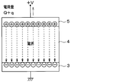
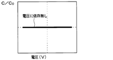
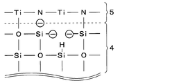
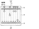
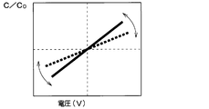
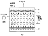
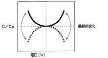
- FIG. 3 is a cross-sectional view showing a manufacturing process of the semiconductor device shown in FIG. 1. It is the figure which showed the electrical characteristics of the MIM capacitor. It is sectional drawing which showed the damage to the capacitive film at the time of forming an upper electrode by PVD method. It is the figure which showed the relationship between the proof pressure of a MIM capacitor, and a Weibull distribution. It is the figure which showed the electrical characteristic of the MIM capacitor in the case of forming an upper electrode by sputtering. It is the figure which showed the mode of the electric charge in the MIM capacitor in an ideal state. It is the figure which showed the electrical characteristic of the MIM capacitor in an ideal state.
- a first embodiment will be described.
- the MIM capacitor will be described by taking a plate structure as an example.
- the semiconductor device having the MIM capacitor described here is applied to, for example, an analog-digital converter (hereinafter referred to as an A / D converter).
- the MIM capacitor is formed on a semiconductor substrate 1 such as a silicon substrate with an insulating film 2 interposed therebetween.
- the MIM capacitor is configured by laminating the lower electrode 3, the capacitor film 4 and the upper electrode 5 in this order on the insulating film 2.
- the lower electrode 3 corresponds to the first electrode, is configured using a general electrode material, and has a structure in which a metal oxide film 3 a is formed on one surface in contact with the capacitive film 4.
- the lower electrode 3 is made of aluminum (Al), titanium nitride (TiN), titanium (Ti), copper (Cu), a single layer film such as polysilicon doped with impurities, metal silicide, or aluminum and copper. Are formed by a laminated film of a plurality of electrode materials.
- the metal oxide film 3a is formed by oxidizing the surface of the lower electrode 3 or the like.
- the capacitor film 4 is formed of an insulating film, and is formed in a planar shape on the lower electrode 3 in this embodiment.
- the capacitor film 4 is made of an insulating film such as a silicon oxide film (SiO) or a silicon nitride film (SiN), and has a thickness corresponding to the required capacity.
- the upper electrode 5 corresponds to the second electrode and is made of a general electrode material. That is, like the lower electrode 3, the upper electrode 5 is formed of a single layer film such as aluminum, titanium nitride, titanium, or copper, or a laminated film of a plurality of electrode materials such as aluminum and copper.
- the upper electrode 5 may be made of the same material as the lower electrode 3 or may be made of a different material.
- One surface of the upper electrode 5 on the side in contact with the capacitance film 4 is constituted by a first layer 5a formed by a CVD method or an atomic layer deposition (hereinafter referred to as ALD (abbreviation of atomic layer deposition)) method.
- ALD abbreviation of atomic layer deposition
- the side of the upper electrode 5 opposite to the capacitor film 4 with respect to the first layer 5a is formed by a second layer 5b formed by a physical vapor deposition (hereinafter referred to as PVD (Physical Vapor Deposition)) method such as sputtering. It is configured.
- the second layer 5b can be formed of tungsten (W), a metal material having a low stress, or polysilicon.
- TEOS TetraylEthylOrthoSilicate
- a semiconductor device including the MIM capacitor according to the present embodiment is configured.
- the MIM capacitor provided in the semiconductor device configured as described above has a wiring (not shown) connected to the lower electrode 3 and a wiring 8 connected to the upper electrode 5 respectively connected to desired positions of the integrated circuit formed on the semiconductor substrate 1. It is used by being connected to the outside through the pad portion.
- the semiconductor substrate 1 is prepared.
- a substrate on which semiconductor elements constituting an integrated circuit or the like are formed can be used as necessary.
- the lower electrode 3 is formed on the surface of the insulating film 2.
- the lower electrode 3 is formed by a PVD method such as sputtering. Note that although the case where the semiconductor substrate 1 is used as an example is described here, a substrate that is not a semiconductor substrate may be used, and the insulating film 2 may not be formed if an insulating substrate is used.
- a metal oxide film 3 a is formed by oxidizing the surface layer portion of the lower electrode 3.
- the metal oxide film 3a can be formed by performing O 2 plasma oxidation or thermal oxidation, which is CVD mainly composed of O 2 radicals.
- the O 2 plasma oxidation includes an O 2 gas atmosphere included in the process so far.
- the metal oxide film 3a can be formed by O 2 plasma oxidation in an O 2 gas atmosphere included in the dry etching gas.
- dry etching performed during the formation of a semiconductor element, formation of a contact hole (not shown) in the insulating film 2 or dry etching when patterning the lower electrode 3 are applicable.
- the lower electrode 3 can be formed using the above-described materials, but when the lower electrode 3 is made of titanium nitride, a titanium oxide (TiO) film is formed as the metal oxide film 3a.
- TiO titanium oxide
- a capacitive film 4 is formed on the lower electrode 3.
- the capacitor film 4 is formed by forming a silicon oxide film by a CVD method or the like.
- the metal oxide film 3a is formed and the metal oxide film 3a is formed by the oxidation of the lower electrode 3 itself, so that the capacitor film 4 formed thereon is formed. It becomes possible to suppress damage. That is, when the lower electrode 3 is simply formed, the capacitance film 4 formed with the lower electrode 3 as a base becomes non-uniform due to roughness of the surface of the lower electrode 3, that is, unevenness. Damage is imparted to the film, which degrades the film quality.
- the roughness cannot be improved when a metal oxide film made of a metal different from the lower electrode 3 is formed on the lower electrode 3.
- the one surface side of the lower electrode 3 as the metal oxide film 3a by the oxidation of the lower electrode 3 itself, it is possible to suppress the nonuniformity of the film thickness of the capacitor film 4 and the deterioration of the film quality.
- the surface unevenness can be reduced and the portion where the electric field is concentrated can be eliminated.
- An upper electrode 5 is formed on the capacitive film 4.
- the first layer 5a is formed by the CVD method or the ALD method, and then the second layer 5b is formed by the PVD method, whereby the upper electrode 5 is formed.
- the first layer 5a is formed by a CVD method or an ALD method in which damage to the capacitive film 4 is unlikely to occur.
- the entire upper electrode 5 is not formed by the CVD method or the ALD method.
- a second layer 5b is formed on the first layer 5a by the PVD method.
- the second layer 5b formed by the PVD method is less likely to enter impurities and has a lower resistance value than the first layer 5a formed by the CVD method or the ALD method. For this reason, by using a laminated film of the first layer 5a and the second layer 5b, it is possible to reduce the resistance of the upper electrode 5 while suppressing damage to the capacitor film 4.
- the upper electrode 5 and the capacitive film 4 are patterned using a predetermined mask.
- a step of forming an interlayer insulating film 6 on the upper electrode 5 or the like is performed.
- a contact hole 6a is formed in the interlayer insulating film 6 using a predetermined mask, and then a via 7 is formed in the contact hole 6a by embedding a bonding metal material such as a tungsten plug.
- the wiring 8 is formed by patterning with a predetermined mask. Thereby, the semiconductor device having the MIM capacitor shown in FIG. 1 can be manufactured.
- the influence of the electrical characteristics of the MIM capacitor appears as a conversion error in A / D conversion when digital output is performed for an analog input.
- the electrical characteristics of the MIM capacitor have a parabolic relationship as shown in FIG. 3.
- the smaller the capacitance change with respect to the change in voltage applied to the MIM capacitor the better the electrical characteristics.
- the error can also be reduced.
- the roughness of the surface of the lower electrode 3 is inevitably achieved when the lower electrode 3 is formed, and the flatness of the surface of the lower electrode 3 cannot be ensured simply by forming the lower electrode 3 by the PVD method or the like. This causes damage such as defects in the capacitive film 4.
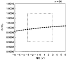
- the electrical characteristics of the MIM capacitor were examined, and the result shown in FIG. 6 was obtained.
- the electric characteristic indicated by the capacitance change C / Co of the MIM capacitor with respect to the voltage (V) applied to the MIM capacitor has a parabolic relationship.
- the linear coefficient in the approximate quadratic function corresponds to the slope of the tangent to the apex of the parabola
- the quadratic coefficient corresponds to the degree of opening of the parabola.
- the primary coefficient was 38.5 ppm / V
- the secondary coefficient was ⁇ 6.9 ppm / V 2 .
- the capacitance change C / Co with respect to the voltage (V) applied to the MIM capacitor is constant at any voltage, and the capacitance change C / Co does not depend on the voltage (V).
- the capacitance change C / Co with respect to the voltage (V) applied to the MIM capacitor that is, the electrical characteristic does not become constant, and an inclination occurs.
- the slope of the electric characteristic is a linear change mainly composed of a first-order coefficient, and changes as indicated by an arrow in the figure depending on the amount of charge trapped.
- the first layer 5a is first formed by the CVD method or the ALD method, so that the capacitor film 4 is formed. Damage can be suppressed, and the electrical characteristics of the MIM capacitor can be made close to constant.
- the breakdown voltage of the capacitive film 4 is compared with the case where damage has occurred. The result that reliability was secured was obtained. Further, when the electrical characteristics of the MIM capacitor were examined in the case of forming the first layer 5a, the electrical characteristics became substantially linear as shown in FIG. When this electric characteristic was approximated by a quadratic function, the primary coefficient in the approximate quadratic function was 21.5 ppm / V, and the secondary coefficient was -1.2 ppm / V 2 . This result also shows that the approximate quadratic function is almost linear.
- damage to the capacitor film 4 particularly affects the electricity of the MIM capacitor.
- the damage to the capacitor film 4 is mainly due to the roughness of the lower electrode 3 and the physical properties when the upper electrode 5 is formed. This is due to damage.
- the roughness due to the roughness of the lower electrode 3 on the capacitance film 4 can be reduced by eliminating the roughness of the lower electrode 3 and further flattening, and the first layer 5a of the upper electrode 5 can be reduced.
- the CVD method or the like physical damage to the capacitive film 4 can be reduced.
- the crystal structure in the capacitive film 4 is in an ordered state, and dangling bonds are reduced.
- a semiconductor device having a capacitor capable of suppressing damage to the capacitor film 4 and improving the reliability of the capacitor film 4 can be used as a manufacturing method.
- the upper electrode 5 is not formed entirely by the CVD method or the like, but the second layer 5b is formed on the first layer 5a by the PVD method or the like, thereby suppressing the resistance of the upper electrode 5 from being increased. It becomes possible.
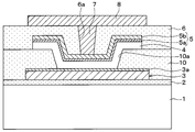
- an interlayer insulating film 10 is formed on the lower electrode 3, and a capacitive film so as to enter a trench 10 a formed so as to penetrate the interlayer insulating film 10. 4 and the upper electrode 5 are formed.
- the lower electrode 3 is exposed from the trench 10a, and the capacitor film 4 and the upper electrode 5 are sequentially stacked so as to be in contact with the exposed portion of the lower electrode 3.
- an interlayer insulating film 6 and a wiring 8 are sequentially formed on the upper electrode 5, and the wiring 8 is electrically connected to the upper electrode 5 through a via 7 formed in the contact hole 6 a of the interlayer insulating film 6.
- the MIM capacitor has a trench structure in which the capacitive film 4 and the upper electrode 5 are formed so as to enter the trench 10a. Also in the MIM capacitor having such a structure, the same effect as that of the first embodiment can be obtained by forming the metal oxide film 3a on the one surface side of the lower electrode 3 or forming the first layer 5a on the upper electrode 5. be able to.
- the manufacturing method of the semiconductor device having the MIM capacitor having such a structure is basically the same as that of the first embodiment, but the manufacturing process of the capacitive film 4 and the upper electrode 5 is the same as that of the first embodiment. It will be changed from the manufacturing method. Specifically, before the step shown in FIG. 2C, the interlayer insulating film 10 is formed by a TEOS film or the like, and then a trench 10a is formed in the interlayer insulating film 10 using a mask (not shown). Then, the process after the process shown in FIG.2 (c) is performed in order. By such a manufacturing method, the semiconductor device having the MIM capacitor of this embodiment can be manufactured.
- a third embodiment will be described.
- a reverse connection capacitor is configured using the MIM capacitor described in the first and second embodiments, and the configuration itself of the MIM capacitor is the same as that of the first and second embodiments. Only differences from the second embodiment will be described.
- two MIM capacitors shown in the first and second embodiments are provided.
- the upper electrode 5 of one MIM capacitor C1 and the lower electrode 3 of the other MIM capacitor C2 are electrically connected, and the lower electrode 3 of one MIM capacitor C1 and the upper electrode 5 of the other MIM capacitor C2 Are electrically connected.
- the respective electrical characteristics can be added. That is, as shown in FIG. 15, the electrical characteristic of one MIM capacitor C1 has a characteristic that the capacitance change C / Co increases based on the increase of the voltage (V), and the electrical characteristic of the other MIM capacitor C1 is the voltage (V ), The capacitance change C / Co decreases. For this reason, when the electric characteristics of these two MIM capacitors C1 and C2 are added together, the electric characteristics of the electric characteristics cancel each other, and the electric power is almost flat. In this way, it is possible to cancel the linear component of the electric characteristics, that is, the primary coefficient, and it is possible to obtain an electric characteristic close to a constant.
- both the formation of the metal oxide film 3a on the one surface side of the lower electrode 3 and the formation of the first layer 5a on the upper electrode 5 are performed.
- the film quality of the capacitive film 4 can be improved.
- the film quality improvement effect of the capacitive film 4 can be further improved, and the reliability of the capacitive film 4 can be further improved.
- the upper electrode 5 has a structure in which the second layer 5b is formed on the first layer 5a, the second layer 5b is not necessarily required. That is, the via 7 may be directly connected to the first layer 5a.
- an insulating film such as a silicon oxide film or a silicon nitride film has been described as an example, but other insulating films such as aluminum oxide (Al 2 O 3 ) may be used.
- a laminated structure of various types of insulating films may be used.
- the first layer 5a in the upper electrode 5 is formed by metal organic chemical vapor deposition (MOCVD (abbreviation of metal-organic chemical vapor deposition)). You may do it.
- MOCVD abbreviation of metal-organic chemical vapor deposition
- the structure in which the first electrode is the lower electrode and the second electrode is the upper electrode has been described.
Landscapes
- Chemical & Material Sciences (AREA)
- Chemical Kinetics & Catalysis (AREA)
- Engineering & Computer Science (AREA)
- Materials Engineering (AREA)
- Mechanical Engineering (AREA)
- Metallurgy (AREA)
- Organic Chemistry (AREA)
- General Chemical & Material Sciences (AREA)
- Inorganic Chemistry (AREA)
- Semiconductor Integrated Circuits (AREA)
- Physical Vapour Deposition (AREA)
- Chemical Vapour Deposition (AREA)
Abstract
下部電極(3)の表面に金属酸化膜(3a)を形成することで、ラフネスを解消して平坦化する。これにより、容量膜(4)への下部電極(3)のラフネスに起因するダメージを軽減できる。また、上部電極(5)の第1層(5a)をCVD法などによって形成することで容量膜(4)への物理的ダメージを軽減する。これにより、容量膜(4)へのダメージを抑制して容量膜(4)の信頼性を高めることができる。また、上部電極(5)をすべてCVD法などによって形成するのではなく、第1層(5a)の上にPVD法などによって第2層(5b)を形成することで、上部電極(5)の高抵抗化を抑制することも可能となる。
Description
本出願は、2016年1月22日に出願された日本特許出願番号2016-10821号に基づくもので、ここにその記載内容が参照により組み入れられる。
本開示は、メタルインシュレータメタル構造のキャパシタ(以下、MIMキャパシタという)を有する半導体装置の製造方法に関するものである。
従来より、下部電極と上部電極との間に容量膜が挟まれることによって構成されるMIMキャパシタが知られている。例えば、特許文献1では、下部電極上に容量膜を成膜したのち、上部電極を化学気相成長(以下、CVD(chemical vapordepositionの略)という)法によって成膜することでMIMキャパシタを製造している。
上記したようにCVD法によって上部電極を成膜する場合、上部電極が高抵抗になってしまう。
上部電極をCVD法によって成膜する場合、下地となる容量膜へのダメージを低減でき、容量膜の信頼性を高めることが可能になるという効果が得られる。このような効果は下地となる容量膜へのダメージの低減によって得られている。したがって、CVD法を用いなくても、容量膜へのダメージを低減できれば上部電極の高抵抗化を抑制しつつ容量膜の信頼性を高めることが可能になる。また、CVD法を用いることで容量膜へのダメージを低減する場合でも、高抵抗化を抑制できる構成とすれば良いし、さらに容量膜へのダメージを抑制できれば、より容量膜の信頼性を向上させることが可能になる。
本開示は、容量膜へのダメージを抑制することで容量膜の信頼性を高めることができる半導体装置の製造方法を提供することを第1の目的とする。さらに、電極の高抵抗化を抑制することができる半導体装置の製造方法を提供することを第2の目的とする。
本開示の1つの観点における半導体装置の製造方法では、第1電極の形成を行うことと、第1電極の上に、該第1電極に接する容量膜を形成することと、容量膜の上に、該容量膜に接する第2電極を形成することと、を含み、第2電極を形成することは、容量膜の表面に化学気相成長、原子層堆積もしくは有機金属気相成長によって第1層を形成することと、第1層の上に物理気相成長によって第2層を形成することを含んでいる。
このように、容量膜の表面に化学気相成長、原子層堆積もしくは有機金属気相成長による第1層を形成しているため、容量膜へのダメージを抑制することができる。また、第2電極をすべて化学気相成長、原子層堆積もしくは有機金属気相成長によって形成するのではなく、第1層の上に物理気相成長法によって第2層を形成することで、第2電極の高抵抗化を抑制することも可能となる。したがって、容量膜へのダメージを抑制することができ、容量膜の信頼性を高めることができる半導体装置の製造方法とすることが可能となる。
また、本開示のもう1つの観点における半導体装置の製造方法では、第1電極の形成を行うことと、第1電極の上に、該第1電極に接する容量膜を形成することと、容量膜の上に、該容量膜に接する第2電極を形成することと、を含み、第1電極を形成することは、該第1電極のうち容量膜側の一面に金属酸化膜を形成することを含んでいる。
このように、第1電極のうちの容量膜側の一面に金属酸化膜を形成することで、第1電極のラフネスを解消してより平坦化することが可能となり、容量膜への第1電極のラフネスに起因するダメージを軽減できる。したがって、容量膜へのダメージを抑制することができ、容量膜の信頼性を高めることができる半導体装置の製造方法とすることが可能となる。
以下、本開示の実施形態について図に基づいて説明する。なお、以下の各実施形態相互において、互いに同一もしくは均等である部分には、同一符号を付して説明を行う。
(第1実施形態)
第1実施形態について説明する。本実施形態では、MIMキャパシタとして、平板構造のものを例に挙げて説明する。なお、ここで説明するMIMキャパシタを有する半導体装置は、例えばアナログデジタルコンバータ(以下、A/Dコンバータという)などに適用される。
第1実施形態について説明する。本実施形態では、MIMキャパシタとして、平板構造のものを例に挙げて説明する。なお、ここで説明するMIMキャパシタを有する半導体装置は、例えばアナログデジタルコンバータ(以下、A/Dコンバータという)などに適用される。
図1に示すように、MIMキャパシタは、例えば、シリコン基板などの半導体基板1の上に絶縁膜2を介して形成される。具体的には、絶縁膜2の上に、下部電極3と容量膜4および上部電極5をその順番に積層することによってMIMキャパシタが構成される。
下部電極3は、第1電極に相当するものであり、一般的な電極材料を用いて構成されており、容量膜4と接する側の一面に金属酸化膜3aが形成された構造とされている。例えば、下部電極3は、アルミニウム(Al)、窒化チタン(TiN)、チタン(Ti)、銅(Cu)、不純物がドープされたポリシリコン、金属シリサイドなどの単層膜、もしくは、アルミニウムと銅などの複数の電極材料の積層膜によって形成されている。そして、下部電極3の表面が酸化されることなどによって金属酸化膜3aが構成されている。
容量膜4は、絶縁膜によって構成されており、本実施形態では下部電極3の上に平面状に形成されている。例えば、容量膜4は、シリコン酸化膜(SiO)、シリコン窒化膜(SiN)等の絶縁膜により構成され、必要とされる容量に応じた膜厚とされている。
上部電極5は、第2電極に相当するものであり、一般的な電極材料で構成されている。すなわち、上部電極5は、下部電極3と同様に、アルミニウム、窒化チタン、チタン、銅などの単層膜、もしくは、アルミニウムと銅などの複数の電極材料の積層膜によって形成されている。上部電極5は、下部電極3と同じ材料で構成されていても異なる材料で構成されていても良い。上部電極5のうち容量膜4と接する側の一面はCVD法もしくは原子層堆積(以下、ALD(Atomic layerdepositionの略)という)法によって形成された第1層5aによって構成されている。また、上部電極5のうち第1層5aに対して容量膜4と反対側は、スパッタリング等の物理気相成長(以下、PVD(Physical VaporDepositionの略))法によって形成された第2層5bによって構成されている。第2層5bについては、さらにタングステン(W)や応力が低い金属材料、もしくはポリシリコンなどによって形成することもできる。
さらに、MIMキャパシタを覆うように、つまり下部電極3と容量膜4および上部電極5の積層構造を覆うように、テトラエトキシシラン(以下、TEOS(Tetra EthylOrthoSilicateの略)という)膜などで構成された層間絶縁膜6が形成されている。そして、層間絶縁膜6のコンタクトホール6a内にタングステンプラグなどの接合金属材料が埋め込まれたビア7が形成され、層間絶縁膜6の上に形成されたアルミニウムなどで構成される配線8と上部電極5とが電気的に接続されている。
このような構造によって、本実施形態にかかるMIMキャパシタを備えた半導体装置が構成されている。このように構成される半導体装置に備えられたMIMキャパシタは、下部電極3に繋がる図示しない配線や上部電極5に接続される配線8がそれぞれ半導体基板1に形成される集積回路の所望位置に接続されたり、パッド部を通じて外部に接続されることで使用される。
続いて、図1に示すMIMキャパシタを有する半導体装置の製造方法について、図2を参照して説明する。
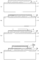
〔図2(a)に示す工程〕
まず、半導体基板1を用意する。半導体基板1としては、必要に応じて集積回路などを構成する半導体素子などが形成されたものを用いることができる。そして、半導体基板1の上に絶縁膜2を形成したのち、絶縁膜2の表面に下部電極3を形成する。例えば、スパッタリング等のPVD法によって下部電極3を形成している。なお、ここでは基板として半導体基板1を用いる場合を例に挙げているが、半導体基板ではない基板を用いても良く、絶縁基板を用いれば絶縁膜2を形成しなくても良い。
まず、半導体基板1を用意する。半導体基板1としては、必要に応じて集積回路などを構成する半導体素子などが形成されたものを用いることができる。そして、半導体基板1の上に絶縁膜2を形成したのち、絶縁膜2の表面に下部電極3を形成する。例えば、スパッタリング等のPVD法によって下部電極3を形成している。なお、ここでは基板として半導体基板1を用いる場合を例に挙げているが、半導体基板ではない基板を用いても良く、絶縁基板を用いれば絶縁膜2を形成しなくても良い。
〔図2(b)に示す工程〕
下部電極3の表層部を酸化することで金属酸化膜3aを形成する。例えば、O2ラジカルを主体とするCVDであるO2プラズマ酸化または熱酸化などを実施することによって、金属酸化膜3aを形成することができる。なお、O2プラズマ酸化としては、ここまでのプロセス中に含まれるO2ガス雰囲気によるものも含まれる。例えば、ここまでのプロセス中にドライエッチングが含まれている場合、ドライエッチングガス中に含まれるO2ガス雰囲気によるO2プラズマ酸化によって金属酸化膜3aを形成することもできる。一例を挙げると、半導体素子の形成中に実施されるドライエッチングや、絶縁膜2に対する図示しないコンタクトホールの形成もしくは下部電極3をパターニングする際のドライエッチングなどが該当する。
下部電極3の表層部を酸化することで金属酸化膜3aを形成する。例えば、O2ラジカルを主体とするCVDであるO2プラズマ酸化または熱酸化などを実施することによって、金属酸化膜3aを形成することができる。なお、O2プラズマ酸化としては、ここまでのプロセス中に含まれるO2ガス雰囲気によるものも含まれる。例えば、ここまでのプロセス中にドライエッチングが含まれている場合、ドライエッチングガス中に含まれるO2ガス雰囲気によるO2プラズマ酸化によって金属酸化膜3aを形成することもできる。一例を挙げると、半導体素子の形成中に実施されるドライエッチングや、絶縁膜2に対する図示しないコンタクトホールの形成もしくは下部電極3をパターニングする際のドライエッチングなどが該当する。
下部電極3については、上記した材料を用いて形成できるが、下部電極3を窒化チタンによって構成する場合には、金属酸化膜3aとして酸化チタン(TiO)膜が形成される。
〔図2(c)に示す工程〕
下部電極3の上に容量膜4を成膜する。例えばCVD法などでシリコン酸化膜を形成することによって容量膜4を形成している。このとき、図2(b)の工程において、金属酸化膜3aを形成し、かつ、下部電極3自身の酸化によって金属酸化膜3aを形成していることから、その上に形成される容量膜4のダメージを抑制することが可能となる。すなわち、単に下部電極3を成膜しただけだと下部電極3の表面のラフネス、つまり凹凸によって、下部電極3を下地として形成される容量膜4が不均一な膜厚になるなど、容量膜4にダメージが付与されて膜質を低下させることになる。また、下部電極3の上に、下部電極3とは別の金属による金属酸化膜を形成するような場合も、ラフネスを改善することができない。これに対して、下部電極3の一面側を下部電極3自身の酸化による金属酸化膜3aとしておくことで、容量膜4の膜厚の不均一や膜質の低下を抑制できる。また、容量膜4にリークポイントとなるピンホールが形成されることを抑制することも可能となり、初期故障なども抑制できる。そして、下部電極3の一面側に積極的に金属酸化膜3aを形成することで、表面の凹凸が低減できて電界集中する部分を無くすことも可能となる。
下部電極3の上に容量膜4を成膜する。例えばCVD法などでシリコン酸化膜を形成することによって容量膜4を形成している。このとき、図2(b)の工程において、金属酸化膜3aを形成し、かつ、下部電極3自身の酸化によって金属酸化膜3aを形成していることから、その上に形成される容量膜4のダメージを抑制することが可能となる。すなわち、単に下部電極3を成膜しただけだと下部電極3の表面のラフネス、つまり凹凸によって、下部電極3を下地として形成される容量膜4が不均一な膜厚になるなど、容量膜4にダメージが付与されて膜質を低下させることになる。また、下部電極3の上に、下部電極3とは別の金属による金属酸化膜を形成するような場合も、ラフネスを改善することができない。これに対して、下部電極3の一面側を下部電極3自身の酸化による金属酸化膜3aとしておくことで、容量膜4の膜厚の不均一や膜質の低下を抑制できる。また、容量膜4にリークポイントとなるピンホールが形成されることを抑制することも可能となり、初期故障なども抑制できる。そして、下部電極3の一面側に積極的に金属酸化膜3aを形成することで、表面の凹凸が低減できて電界集中する部分を無くすことも可能となる。
〔図2(d)に示す工程〕
容量膜4の上に上部電極5を成膜する。このとき、まず最初にCVD法もしくはALD法によって第1層5aを形成し、その後、PVD法によって第2層5bを形成することで上部電極5を成膜している。
容量膜4の上に上部電極5を成膜する。このとき、まず最初にCVD法もしくはALD法によって第1層5aを形成し、その後、PVD法によって第2層5bを形成することで上部電極5を成膜している。
容量膜4の上に直接PVD法によって上部電極5を形成すると、容量膜4にダメージが生じる。このため、まずは容量膜4へのダメージが発生し難いCVD法もしくはALD法によって第1層5aを形成する。ただし、CVD法もしくはALD法によって形成される第1層5aは不純物が入り易く、低抵抗化を図ることが難しいため、上部電極5のすべてをCVD法もしくはALD法によって形成するのではなく、第1層5aの上にPVD法による第2層5bを形成する。PVD法によって形成される第2層5bは、CVD法やALD法によって形成される第1層5aと比較して不純物が入り込み難く抵抗値が低い。このため、第1層5aと第2層5bとの積層膜とすることで、容量膜4へのダメージを抑制しつつ、上部電極5の低抵抗化を図ることが可能となる。
この後、例えば所定のマスクを用いて上部電極5および容量膜4をパターニングする。この後の工程については図示しないが、上部電極5等の上に層間絶縁膜6を形成する工程を行う。そして、所定のマスクを用いて層間絶縁膜6に対してコンタクトホール6aを形成したのち、コンタクトホール6a内にタングステンプラグなどの接合金属材料の埋め込み工程を行うことでビア7を形成する。さらに、層間絶縁膜6の上にアルミニウムなどの金属層を成膜したのち、所定のマスクによってパターニングすることで配線8を形成する。これにより、図1に示したMIMキャパシタを有する半導体装置を製造することができる。
ここで、MIMキャパシタにおける容量-電圧特性(以下、電特という)の変化メカニズムについて説明する。
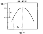
MIMキャパシタをA/Dコンバータに適用した場合、アナログ入力に対してデジタル出力を行うにあたり、MIMキャパシタの電特の影響がA/D変換の変換誤差として表れる。例えばMIMキャパシタの電特は図3のように放物線状の関係となるが、MIMキャパシタに印加される電圧の変化に対して容量変化が小さいほど電特が良好であり、A/D変換の変換誤差も小さくすることができる。このため、A/DコンバータにMIMキャパシタを適用する場合には、MIMキャパシタの電特を良好にすることが重要であり、それによってA/Dコンバータの変換精度を高精度にすることが可能になる。
このMIMキャパシタの電特について調べたところ、容量膜4の膜質が影響していることが確認された。すなわち、容量膜4にダメージが入っていて、容量膜4の膜質が良好でないと、そのダメージが影響してMIMキャパシタの電特が悪化することが確認された。そして、その原因について調べたところ、1つは容量膜4の上に形成する上部電極5をPVD法によって形成していることが原因であることが判り、もう一つは容量膜4を形成する際の下地となる下部電極3の表面のラフネスが原因であることが判った。
下部電極3の表面のラフネスについては、下部電極3を形成すると必然的にできるものであり、単純にPVD法などによって下部電極3を形成しただけでは下部電極3の表面の平坦性を担保できない。これが原因となって、容量膜4に欠陥などのダメージが発生することになる。
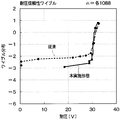
また、容量膜4の上にPVD法、例えばスパッタリングによって上部電極5を形成した場合、図4に示すようにスパッタリングによる物理的ダメージが発生する。特に、容量膜4中に欠陥などに起因して強度的に弱い部分が存在すると、スパッタリングによる物理的ダメージの進行を助長させる。スパッタリングを行った後のMIMキャパシタの試料について、耐圧とワイブル分布を確認したところ、図5中破線に示す結果となった。この図に示されるように、良品であれば30[V]以上の耐圧が得られるのに対して、30[V]未満の耐圧しか得られない試料も複数存在していた。この結果からも、スパッタリングによるダメージに起因して容量膜4の信頼性が低下し、所望の耐圧が得られていないことが分かる。
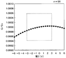
また、容量膜4の上にPVD法、例えばスパッタリングによって上部電極5を形成した場合において、MIMキャパシタの電特を調べたところ、図6の結果となった。この図に示すように、MIMキャパシタに印加する電圧(V)に対するMIMキャパシタの容量変化C/Coで示される電特が放物線状の関係となる。この電特における破線で囲んだ部分を二次関数近似したときに、近似二次関数における一次係数は放物線の頂点に対する接線の傾きと対応し、二次係数は放物線の開き具合と対応している。図6に示される電特においては、一次係数が38.5ppm/V、二次係数が-6.9ppm/V2となった。
MIMキャパシタでは、容量膜4に欠陥が無い理想状態であれば、図7Aに示すように下部電極3と上部電極5との電荷がバランスする。このため、図7Bに示すようにMIMキャパシタに印加する電圧(V)に対する容量変化C/Coがどの電圧においても一定となり、容量変化C/Coが電圧(V)に依存しないという電特になる。
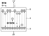
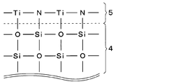
しかしながら、PVD法によって容量膜4を形成したことや下地となる下部電極3のラフネスに基づく容量膜4へのダメージが発生すると、図8に示すように、容量膜4中の結晶構造が壊れ、ダングリングボンド、つまり未接合手が発生する。このダングリングボンドに電荷がトラップされ、MIMキャパシタの電特の変化が大きくなる。このため、図9Aおよび図9Bに示すように、上部電極5に対してマイナス電位をバイアスしたときも、プラス電位をバイアスしたときにも、バイアスの正負に依存して電荷が増減する。この影響で、図9Cに示すように、MIMキャパシタに印加する電圧(V)に対する容量変化C/Co、つまり電特が一定とならずに傾きが生じる。この電特の傾きは一次係数を主体とした線形的な変化となり、トラップされる電荷量などによって図中矢印で示したように変わる。
また、容量膜4中に欠陥が存在すると、図10Aに示すように、その欠陥による配向分極による電界打消しが生じる。これにより、図10Bに示すように、二次係数を主体として電特が図中矢印で示したように曲線変化する。
このように、容量膜4の欠陥の存在により、一次係数および二次係数が変化し、MIMキャパシタの電特が一定にならない。
したがって、上記したように、下部電極3に金属酸化膜3aを形成したり、上部電極5を形成する際に最初にCVD法もしくはALD法によって第1層5aを形成することで、容量膜4へのダメージを抑制でき、MIMキャパシタの電特を一定に近づけることができる。
そして、第1層5aを形成することで容量膜4へのダメージの発生を抑制した場合、図5中実線で示すように、ダメージが発生している場合と比較して、容量膜4の耐圧信頼性を確保できるという結果が得られた。また、第1層5aを形成する場合においてMIMキャパシタの電特を調べたところ、図11に示すように、電特がほぼ直線状になった。この電特を二次関数近似すると、近似二次関数における一次係数が21.5ppm/V、二次係数が-1.2ppm/V2となった。この結果からも、近似二次関数がほぼ直線状になっていることが判る。
このように、容量膜4へのダメージがMIMキャパシタの電特に影響を与えており、容量膜4へのダメージは、主に、下部電極3のラフネスによるものと上部電極5の形成時の物理的ダメージによるものである。
したがって、上記したように、下部電極3のラフネスを解消してより平坦化することで、容量膜4への下部電極3のラフネスに起因するダメージを軽減でき、上部電極5の第1層5aをCVD法などによって形成することで容量膜4への物理的ダメージを軽減できる。例えば、図12に示すように、容量膜4中の結晶構造が整った状態となり、ダングリングボンドが減少する。これにより、容量膜4へのダメージを抑制して容量膜4の信頼性を高めることができるキャパシタを有する半導体装置を製造方法とすることが可能となる。また、上部電極5をすべてCVD法などによって形成するのではなく、第1層5aの上にPVD法などによって第2層5bを形成することで、上部電極5の高抵抗化を抑制することも可能となる。
このようにして、容量膜4へのダメージを抑制することができ、容量膜4の信頼性を高めることができる半導体装置の製造方法とすることが可能となる。
(第2実施形態)
第2実施形態について説明する。本実施形態は、第1実施形態に対して容量膜4や上部電極5の構造を変更したものであり、その他については第1実施形態と同様であるため、第1実施形態と異なる部分についてのみ説明する。
第2実施形態について説明する。本実施形態は、第1実施形態に対して容量膜4や上部電極5の構造を変更したものであり、その他については第1実施形態と同様であるため、第1実施形態と異なる部分についてのみ説明する。
図13に示すように、本実施形態では、下部電極3の上に層間絶縁膜10が形成されており、この層間絶縁膜10を貫通するように形成されたトレンチ10a内に入り込むように容量膜4および上部電極5が形成されている。トレンチ10aからは下部電極3が露出させられており、下部電極3のうち露出させられている部分に接するように容量膜4および上部電極5が順に積層されている。そして、さらに上部電極5の上に層間絶縁膜6と配線8が順に形成されており、層間絶縁膜6のコンタクトホール6a内に形成されたビア7を通じて配線8が上部電極5と電気的に接続されている。
このように、本実施形態では、トレンチ10a内に容量膜4および上部電極5が入り込むように形成されたトレンチ構造のMIMキャパシタとしている。このような構造のMIMキャパシタにおいても、下部電極3の一面側に金属酸化膜3aを形成したり、上部電極5に第1層5aを形成することで、第1実施形態と同様の効果を得ることができる。
なお、このような構造のMIMキャパシタを有する半導体装置の製造方法は、基本的には第1実施形態と同様であるが、容量膜4や上部電極5などの製造工程については第1実施形態の製造方法から変更することになる。具体的には、図2(c)に示す工程の前に、TEOS膜などによって層間絶縁膜10を成膜したのち、図示しないマスクを用いて層間絶縁膜10に対してトレンチ10aを形成する。その後、図2(c)に示す工程以降の工程を順に行う。このような製造方法により、本実施形態のMIMキャパシタを有する半導体装置を製造することができる。
(第3実施形態)
第3実施形態について説明する。本実施形態は、第1、第2実施形態で説明したMIMキャパシタを用いて逆接キャパシタを構成するものであり、MIMキャパシタの構成自体は第1、第2実施形態と同様であるため、第1、第2実施形態と異なる部分についてのみ説明する。
第3実施形態について説明する。本実施形態は、第1、第2実施形態で説明したMIMキャパシタを用いて逆接キャパシタを構成するものであり、MIMキャパシタの構成自体は第1、第2実施形態と同様であるため、第1、第2実施形態と異なる部分についてのみ説明する。
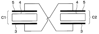
図14に示すように、本実施形態では、第1、第2実施形態で示したMIMキャパシタを2つ備えている。そして、一方のMIMキャパシタC1の上部電極5と他方のMIMキャパシタC2の下部電極3とを電気的に接続するとともに、一方のMIMキャパシタC1の下部電極3と他方のMIMキャパシタC2の上部電極5とを電気的に接続している。
このように、2つのMIMキャパシタC1、C2を互いに逆接続することで、それぞれの電特を足し合わせることができる。すなわち、図15に示すように、一方のMIMキャパシタC1の電特が電圧(V)の増加に基づいて容量変化C/Coが増加する特性となり、他方のMIMキャパシタC1の電特が電圧(V)の増加に基づいて容量変化C/Coが減少する特性となる。このため、これら2つのMIMキャパシタC1、C2の電特を足し合わせると、互いの電特の傾斜が打ち消しあい、平坦に近い電特になる。このように、電特の直線成分、つまり一次係数を相殺することが可能となり、一定に近い電特を得ることが可能となる。
(他の実施形態)
本開示は、上記した実施形態に準拠して記述されたが、当該実施形態に限定されるものではなく、様々な変形例や均等範囲内の変形をも包含する。加えて、様々な組み合わせや形態、さらには、それらに一要素のみ、それ以上、あるいはそれ以下、を含む他の組み合わせや形態をも、本開示の範疇や思想範囲に入るものである。
本開示は、上記した実施形態に準拠して記述されたが、当該実施形態に限定されるものではなく、様々な変形例や均等範囲内の変形をも包含する。加えて、様々な組み合わせや形態、さらには、それらに一要素のみ、それ以上、あるいはそれ以下、を含む他の組み合わせや形態をも、本開示の範疇や思想範囲に入るものである。
例えば、上記各実施形態では、下部電極3の一面側に金属酸化膜3aを形成することと、上部電極5に第1層5aを形成することの両方を行うようにしているが、少なくとも一方を行うことで、容量膜4の膜質の改善をできる。ただし、両方共に行うことで、より容量膜4の膜質の改善効果を向上させられ、より容量膜4の信頼性を高めることが可能となる。
また、上部電極5を第1層5aの上に第2層5bを形成する構造としたが、第2層5bについては必ずしも必要ではない。つまり、第1層5aに対して直接ビア7が接続される構造であっても良い。
また、容量膜4の構成材料として、シリコン酸化膜、シリコン窒化膜などの絶縁膜を例に挙げたが、酸化アルミニウム(Al2O3)などの他の絶縁膜であっても良いし、複数種類の絶縁膜の積層構造であっても良い。
また、上部電極5における第1層5aの成膜方法として、CVD法やALD法を例に挙げたが、有機金属気相成長(MOCVD(metal organicchemicalvapordepositionの略))法によって第1層5aを形成しても良い。
なお、上記実施形態では、第1電極を下部電極、第2電極を上部電極とする構造について説明したが、これは一例であり、本開示は、メタルインシュレータメタル構造のキャパシタを構成する第1電極と第2電極とを備えた構造に対して適用可能である。
Claims (6)
- メタルインシュレータメタル構造のキャパシタを有する半導体装置の製造方法であって、
第1電極(3)の形成を行うことと、
前記第1電極の上に、該第1電極に接する容量膜(4)を形成することと、
前記容量膜の上に、該容量膜に接する第2電極(5)を形成することと、を含み、
前記第2電極を形成することは、前記容量膜の表面に化学気相成長、原子層堆積もしくは有機金属気相成長によって第1層(5a)を形成することと、前記第1層の上に物理気相成長によって第2層(5b)を形成することを含んでいる半導体装置の製造方法。 - 前記第1層を形成することは、該第1層として、アルミニウム、窒化チタン、チタン、銅のいずれか1つで構成される単層膜もしくは複数で構成される積層膜を形成することである請求項1に記載の半導体装置の製造方法。
- 前記第2層を形成することは、該第2層として、アルミニウム、窒化チタン、チタン、銅、タングステンのいずれかによって構成される膜を形成することである請求項1または2に記載の半導体装置の製造方法。
- 前記第1電極を形成することは、該第1電極のうち前記容量膜側の一面に金属酸化膜(3a)を形成することを含んでいる請求項1ないし3のいずれか1つに記載の半導体装置の製造方法。
- メタルインシュレータメタル構造のキャパシタを有する半導体装置の製造方法であって、
第1電極(3)の形成を行うことと、
前記第1電極の上に、該第1電極に接する容量膜(4)を形成することと、
前記容量膜の上に、該容量膜に接する第2電極(5)を形成することと、を含み、
前記第1電極を形成することは、該第1電極のうち前記容量膜側の一面に金属酸化膜(3a)を形成することを含んでいる半導体装置の製造方法。 - 前記金属酸化膜を形成することは、前記第1電極の一面に対してO2ラジカルを主体とするCVDであるO2プラズマ酸化を行うこと、または熱酸化を行うことで前記金属酸化膜を形成することを含んでいる請求項4または5に記載の半導体装置の製造方法。
Priority Applications (1)
| Application Number | Priority Date | Filing Date | Title |
|---|---|---|---|
| US15/777,681 US10403709B2 (en) | 2016-01-22 | 2016-11-17 | Method for manufacturing semiconductor device |
Applications Claiming Priority (2)
| Application Number | Priority Date | Filing Date | Title |
|---|---|---|---|
| JP2016-010821 | 2016-01-22 | ||
| JP2016010821A JP6583014B2 (ja) | 2016-01-22 | 2016-01-22 | 半導体装置の製造方法 |
Publications (1)
| Publication Number | Publication Date |
|---|---|
| WO2017126207A1 true WO2017126207A1 (ja) | 2017-07-27 |
Family
ID=59362060
Family Applications (1)
| Application Number | Title | Priority Date | Filing Date |
|---|---|---|---|
| PCT/JP2016/084092 Ceased WO2017126207A1 (ja) | 2016-01-22 | 2016-11-17 | 半導体装置の製造方法 |
Country Status (3)
| Country | Link |
|---|---|
| US (1) | US10403709B2 (ja) |
| JP (1) | JP6583014B2 (ja) |
| WO (1) | WO2017126207A1 (ja) |
Families Citing this family (2)
| Publication number | Priority date | Publication date | Assignee | Title |
|---|---|---|---|---|
| JP2018120123A (ja) * | 2017-01-26 | 2018-08-02 | 株式会社ジャパンディスプレイ | 表示装置及び基板間導通構造 |
| JP6888581B2 (ja) | 2018-04-11 | 2021-06-16 | 株式会社デンソー | 半導体装置およびその製造方法 |
Citations (6)
| Publication number | Priority date | Publication date | Assignee | Title |
|---|---|---|---|---|
| JP2001200363A (ja) * | 1999-12-03 | 2001-07-24 | Asm Microchemistry Oy | テクスチャ加工されたキャパシタ電極上のコンフォーマル薄膜 |
| JP2004064091A (ja) * | 2002-07-30 | 2004-02-26 | Samsung Electronics Co Ltd | 半導体装置のキャパシタ及びその製造方法 |
| JP2007134726A (ja) * | 2005-11-12 | 2007-05-31 | Samsung Electronics Co Ltd | Mimキャパシタを備える集積回路装置およびその製造方法 |
| JP2011258832A (ja) * | 2010-06-10 | 2011-12-22 | Renesas Electronics Corp | 半導体装置及び半導体装置の製造方法 |
| JP2012104551A (ja) * | 2010-11-08 | 2012-05-31 | Elpida Memory Inc | 半導体記憶装置及びその製造方法 |
| JP2014154585A (ja) * | 2013-02-05 | 2014-08-25 | Mitsubishi Electric Corp | 半導体装置、半導体装置の製造方法 |
Family Cites Families (11)
| Publication number | Priority date | Publication date | Assignee | Title |
|---|---|---|---|---|
| JPH04241449A (ja) * | 1991-01-16 | 1992-08-28 | Hitachi Ltd | 半導体集積回路装置 |
| JPH11274428A (ja) * | 1998-03-19 | 1999-10-08 | Kawasaki Steel Corp | 半導体装置及びその製造方法 |
| JP3948321B2 (ja) * | 2002-03-26 | 2007-07-25 | 株式会社村田製作所 | 3端子コンデンサの実装構造 |
| KR100480603B1 (ko) | 2002-07-19 | 2005-04-06 | 삼성전자주식회사 | 일정한 커패시턴스를 갖는 금속-절연체-금속 커패시터를 포함하는 반도체 소자 |
| JP4571836B2 (ja) | 2004-07-23 | 2010-10-27 | ルネサスエレクトロニクス株式会社 | 半導体装置およびその製造方法 |
| JP4837943B2 (ja) | 2005-05-30 | 2011-12-14 | ラピスセミコンダクタ株式会社 | 半導体装置およびその製造方法 |
| JP4333642B2 (ja) * | 2005-06-17 | 2009-09-16 | ヤマハ株式会社 | キャパシタ装置及びキャパシタ装置の製造方法 |
| JP2007294848A (ja) * | 2006-03-30 | 2007-11-08 | Eudyna Devices Inc | キャパシタおよび電子回路 |
| KR101712040B1 (ko) | 2009-10-20 | 2017-03-03 | 에이에스엠 인터내셔널 엔.브이. | 유전체 막들의 부동태화를 위한 공정들 |
| EP2434531B1 (en) | 2010-09-28 | 2019-12-04 | IMEC vzw | Method for manufacturing of a metal-insulator-metal capacitor |
| US8952748B2 (en) * | 2013-03-13 | 2015-02-10 | Futurewei Technologies, Inc. | Circuit and method for a multi-mode filter |
-
2016
- 2016-01-22 JP JP2016010821A patent/JP6583014B2/ja active Active
- 2016-11-17 WO PCT/JP2016/084092 patent/WO2017126207A1/ja not_active Ceased
- 2016-11-17 US US15/777,681 patent/US10403709B2/en active Active
Patent Citations (6)
| Publication number | Priority date | Publication date | Assignee | Title |
|---|---|---|---|---|
| JP2001200363A (ja) * | 1999-12-03 | 2001-07-24 | Asm Microchemistry Oy | テクスチャ加工されたキャパシタ電極上のコンフォーマル薄膜 |
| JP2004064091A (ja) * | 2002-07-30 | 2004-02-26 | Samsung Electronics Co Ltd | 半導体装置のキャパシタ及びその製造方法 |
| JP2007134726A (ja) * | 2005-11-12 | 2007-05-31 | Samsung Electronics Co Ltd | Mimキャパシタを備える集積回路装置およびその製造方法 |
| JP2011258832A (ja) * | 2010-06-10 | 2011-12-22 | Renesas Electronics Corp | 半導体装置及び半導体装置の製造方法 |
| JP2012104551A (ja) * | 2010-11-08 | 2012-05-31 | Elpida Memory Inc | 半導体記憶装置及びその製造方法 |
| JP2014154585A (ja) * | 2013-02-05 | 2014-08-25 | Mitsubishi Electric Corp | 半導体装置、半導体装置の製造方法 |
Also Published As
| Publication number | Publication date |
|---|---|
| US20180350897A1 (en) | 2018-12-06 |
| JP6583014B2 (ja) | 2019-10-02 |
| US10403709B2 (en) | 2019-09-03 |
| JP2017130620A (ja) | 2017-07-27 |
Similar Documents
| Publication | Publication Date | Title |
|---|---|---|
| JP2682392B2 (ja) | 薄膜キャパシタおよびその製造方法 | |
| US7915135B2 (en) | Method of making multi-layer structure for metal-insulator-metal capacitor | |
| US9196674B2 (en) | Insulation layer to improve capacitor breakdown voltage | |
| US7872292B2 (en) | Capacitance dielectric layer and capacitor | |
| KR20050028748A (ko) | 적어도 3층의 고유전막들을 갖는 아날로그 커패시터 및그것을 제조하는 방법 | |
| KR20050114035A (ko) | 커패시터 상부에 유동성 절연막을 갖는 반도체소자 및 그제조 방법 | |
| EP3758067B1 (en) | Capacitor and manufacturing method therefor | |
| US7745280B2 (en) | Metal-insulator-metal capacitor structure | |
| JP6583014B2 (ja) | 半導体装置の製造方法 | |
| US20080038895A1 (en) | Capacitor of semiconductor device and method of manufacturing the same | |
| KR101475996B1 (ko) | 유전체, 이를 구비한 캐패시터 및 그 제조방법, 반도체 소자 제조방법 | |
| KR20180027269A (ko) | 박막 커패시터 | |
| TWI622176B (zh) | Mim電容之結構及其製造方法 | |
| CN112018241B (zh) | 半导体结构及其形成方法 | |
| TWI430399B (zh) | 製造供金屬-絕緣體-金屬電容使用之多層結構之方法 | |
| US20070052107A1 (en) | Multi-layered structure and fabricating method thereof and dual damascene structure, interconnect structure and capacitor | |
| JP5396943B2 (ja) | 半導体装置及びその製造方法 | |
| KR100685635B1 (ko) | 반도체 소자의 엠아이엠 캐패시터 형성방법 및 엠아이엠캐패시터 | |
| US7170736B2 (en) | Capacitor having low resistance electrode including a thin silicon layer | |
| CN116705692A (zh) | 半导体结构及半导体制造方法 | |
| KR20040107842A (ko) | TiN 하부 전극을 갖는 반도체 메모리 소자 및 그제조방법 | |
| US6686621B2 (en) | Semiconductor device | |
| TW202401841A (zh) | 金屬絕緣體金屬電容器結構及其製造方法 | |
| CN110730905A (zh) | 半导体装置及其制造方法 | |
| CN100479157C (zh) | 金属-绝缘层-金属电容器的制造方法 |
Legal Events
| Date | Code | Title | Description |
|---|---|---|---|
| 121 | Ep: the epo has been informed by wipo that ep was designated in this application |
Ref document number: 16886446 Country of ref document: EP Kind code of ref document: A1 |
|
| NENP | Non-entry into the national phase |
Ref country code: DE |
|
| 122 | Ep: pct application non-entry in european phase |
Ref document number: 16886446 Country of ref document: EP Kind code of ref document: A1 |