WO2017119216A1 - 電子部品ハンドリングユニット - Google Patents
電子部品ハンドリングユニット Download PDFInfo
- Publication number
- WO2017119216A1 WO2017119216A1 PCT/JP2016/085287 JP2016085287W WO2017119216A1 WO 2017119216 A1 WO2017119216 A1 WO 2017119216A1 JP 2016085287 W JP2016085287 W JP 2016085287W WO 2017119216 A1 WO2017119216 A1 WO 2017119216A1
- Authority
- WO
- WIPO (PCT)
- Prior art keywords
- pickup
- mounting
- tool
- semiconductor chip
- unit
- Prior art date
Links
Images


Classifications
-
- H—ELECTRICITY
- H01—ELECTRIC ELEMENTS
- H01L—SEMICONDUCTOR DEVICES NOT COVERED BY CLASS H10
- H01L21/00—Processes or apparatus adapted for the manufacture or treatment of semiconductor or solid state devices or of parts thereof
- H01L21/67—Apparatus specially adapted for handling semiconductor or electric solid state devices during manufacture or treatment thereof; Apparatus specially adapted for handling wafers during manufacture or treatment of semiconductor or electric solid state devices or components ; Apparatus not specifically provided for elsewhere
- H01L21/67005—Apparatus not specifically provided for elsewhere
- H01L21/67011—Apparatus for manufacture or treatment
- H01L21/67144—Apparatus for mounting on conductive members, e.g. leadframes or conductors on insulating substrates
-
- H—ELECTRICITY
- H01—ELECTRIC ELEMENTS
- H01L—SEMICONDUCTOR DEVICES NOT COVERED BY CLASS H10
- H01L21/00—Processes or apparatus adapted for the manufacture or treatment of semiconductor or solid state devices or of parts thereof
- H01L21/67—Apparatus specially adapted for handling semiconductor or electric solid state devices during manufacture or treatment thereof; Apparatus specially adapted for handling wafers during manufacture or treatment of semiconductor or electric solid state devices or components ; Apparatus not specifically provided for elsewhere
- H01L21/67005—Apparatus not specifically provided for elsewhere
- H01L21/67011—Apparatus for manufacture or treatment
- H01L21/67121—Apparatus for making assemblies not otherwise provided for, e.g. package constructions
-
- H—ELECTRICITY
- H01—ELECTRIC ELEMENTS
- H01L—SEMICONDUCTOR DEVICES NOT COVERED BY CLASS H10
- H01L21/00—Processes or apparatus adapted for the manufacture or treatment of semiconductor or solid state devices or of parts thereof
- H01L21/67—Apparatus specially adapted for handling semiconductor or electric solid state devices during manufacture or treatment thereof; Apparatus specially adapted for handling wafers during manufacture or treatment of semiconductor or electric solid state devices or components ; Apparatus not specifically provided for elsewhere
- H01L21/677—Apparatus specially adapted for handling semiconductor or electric solid state devices during manufacture or treatment thereof; Apparatus specially adapted for handling wafers during manufacture or treatment of semiconductor or electric solid state devices or components ; Apparatus not specifically provided for elsewhere for conveying, e.g. between different workstations
- H01L21/67703—Apparatus specially adapted for handling semiconductor or electric solid state devices during manufacture or treatment thereof; Apparatus specially adapted for handling wafers during manufacture or treatment of semiconductor or electric solid state devices or components ; Apparatus not specifically provided for elsewhere for conveying, e.g. between different workstations between different workstations
- H01L21/67712—Apparatus specially adapted for handling semiconductor or electric solid state devices during manufacture or treatment thereof; Apparatus specially adapted for handling wafers during manufacture or treatment of semiconductor or electric solid state devices or components ; Apparatus not specifically provided for elsewhere for conveying, e.g. between different workstations between different workstations the substrate being handled substantially vertically
-
- H—ELECTRICITY
- H01—ELECTRIC ELEMENTS
- H01L—SEMICONDUCTOR DEVICES NOT COVERED BY CLASS H10
- H01L21/00—Processes or apparatus adapted for the manufacture or treatment of semiconductor or solid state devices or of parts thereof
- H01L21/67—Apparatus specially adapted for handling semiconductor or electric solid state devices during manufacture or treatment thereof; Apparatus specially adapted for handling wafers during manufacture or treatment of semiconductor or electric solid state devices or components ; Apparatus not specifically provided for elsewhere
- H01L21/677—Apparatus specially adapted for handling semiconductor or electric solid state devices during manufacture or treatment thereof; Apparatus specially adapted for handling wafers during manufacture or treatment of semiconductor or electric solid state devices or components ; Apparatus not specifically provided for elsewhere for conveying, e.g. between different workstations
- H01L21/67703—Apparatus specially adapted for handling semiconductor or electric solid state devices during manufacture or treatment thereof; Apparatus specially adapted for handling wafers during manufacture or treatment of semiconductor or electric solid state devices or components ; Apparatus not specifically provided for elsewhere for conveying, e.g. between different workstations between different workstations
- H01L21/67721—Apparatus specially adapted for handling semiconductor or electric solid state devices during manufacture or treatment thereof; Apparatus specially adapted for handling wafers during manufacture or treatment of semiconductor or electric solid state devices or components ; Apparatus not specifically provided for elsewhere for conveying, e.g. between different workstations between different workstations the substrates to be conveyed not being semiconductor wafers or large planar substrates, e.g. chips, lead frames
-
- H—ELECTRICITY
- H01—ELECTRIC ELEMENTS
- H01L—SEMICONDUCTOR DEVICES NOT COVERED BY CLASS H10
- H01L24/00—Arrangements for connecting or disconnecting semiconductor or solid-state bodies; Methods or apparatus related thereto
- H01L24/74—Apparatus for manufacturing arrangements for connecting or disconnecting semiconductor or solid-state bodies
- H01L24/75—Apparatus for connecting with bump connectors or layer connectors
-
- H—ELECTRICITY
- H05—ELECTRIC TECHNIQUES NOT OTHERWISE PROVIDED FOR
- H05K—PRINTED CIRCUITS; CASINGS OR CONSTRUCTIONAL DETAILS OF ELECTRIC APPARATUS; MANUFACTURE OF ASSEMBLAGES OF ELECTRICAL COMPONENTS
- H05K13/00—Apparatus or processes specially adapted for manufacturing or adjusting assemblages of electric components
- H05K13/04—Mounting of components, e.g. of leadless components
- H05K13/0404—Pick-and-place heads or apparatus, e.g. with jaws
- H05K13/0413—Pick-and-place heads or apparatus, e.g. with jaws with orientation of the component while holding it; Drive mechanisms for gripping tools, e.g. lifting, lowering or turning of gripping tools
-
- H—ELECTRICITY
- H05—ELECTRIC TECHNIQUES NOT OTHERWISE PROVIDED FOR
- H05K—PRINTED CIRCUITS; CASINGS OR CONSTRUCTIONAL DETAILS OF ELECTRIC APPARATUS; MANUFACTURE OF ASSEMBLAGES OF ELECTRICAL COMPONENTS
- H05K13/00—Apparatus or processes specially adapted for manufacturing or adjusting assemblages of electric components
- H05K13/04—Mounting of components, e.g. of leadless components
- H05K13/046—Surface mounting
-
- H—ELECTRICITY
- H01—ELECTRIC ELEMENTS
- H01L—SEMICONDUCTOR DEVICES NOT COVERED BY CLASS H10
- H01L2224/00—Indexing scheme for arrangements for connecting or disconnecting semiconductor or solid-state bodies and methods related thereto as covered by H01L24/00
- H01L2224/74—Apparatus for manufacturing arrangements for connecting or disconnecting semiconductor or solid-state bodies and for methods related thereto
- H01L2224/75—Apparatus for connecting with bump connectors or layer connectors
- H01L2224/7525—Means for applying energy, e.g. heating means
- H01L2224/75251—Means for applying energy, e.g. heating means in the lower part of the bonding apparatus, e.g. in the apparatus chuck
-
- H—ELECTRICITY
- H01—ELECTRIC ELEMENTS
- H01L—SEMICONDUCTOR DEVICES NOT COVERED BY CLASS H10
- H01L2224/00—Indexing scheme for arrangements for connecting or disconnecting semiconductor or solid-state bodies and methods related thereto as covered by H01L24/00
- H01L2224/74—Apparatus for manufacturing arrangements for connecting or disconnecting semiconductor or solid-state bodies and for methods related thereto
- H01L2224/75—Apparatus for connecting with bump connectors or layer connectors
- H01L2224/7525—Means for applying energy, e.g. heating means
- H01L2224/75252—Means for applying energy, e.g. heating means in the upper part of the bonding apparatus, e.g. in the bonding head
-
- H—ELECTRICITY
- H01—ELECTRIC ELEMENTS
- H01L—SEMICONDUCTOR DEVICES NOT COVERED BY CLASS H10
- H01L2224/00—Indexing scheme for arrangements for connecting or disconnecting semiconductor or solid-state bodies and methods related thereto as covered by H01L24/00
- H01L2224/74—Apparatus for manufacturing arrangements for connecting or disconnecting semiconductor or solid-state bodies and for methods related thereto
- H01L2224/75—Apparatus for connecting with bump connectors or layer connectors
- H01L2224/7525—Means for applying energy, e.g. heating means
- H01L2224/753—Means for applying energy, e.g. heating means by means of pressure
- H01L2224/75301—Bonding head
-
- H—ELECTRICITY
- H01—ELECTRIC ELEMENTS
- H01L—SEMICONDUCTOR DEVICES NOT COVERED BY CLASS H10
- H01L2224/00—Indexing scheme for arrangements for connecting or disconnecting semiconductor or solid-state bodies and methods related thereto as covered by H01L24/00
- H01L2224/74—Apparatus for manufacturing arrangements for connecting or disconnecting semiconductor or solid-state bodies and for methods related thereto
- H01L2224/75—Apparatus for connecting with bump connectors or layer connectors
- H01L2224/7565—Means for transporting the components to be connected
-
- H—ELECTRICITY
- H01—ELECTRIC ELEMENTS
- H01L—SEMICONDUCTOR DEVICES NOT COVERED BY CLASS H10
- H01L2224/00—Indexing scheme for arrangements for connecting or disconnecting semiconductor or solid-state bodies and methods related thereto as covered by H01L24/00
- H01L2224/74—Apparatus for manufacturing arrangements for connecting or disconnecting semiconductor or solid-state bodies and for methods related thereto
- H01L2224/75—Apparatus for connecting with bump connectors or layer connectors
- H01L2224/757—Means for aligning
- H01L2224/75702—Means for aligning in the upper part of the bonding apparatus, e.g. in the bonding head
-
- H—ELECTRICITY
- H01—ELECTRIC ELEMENTS
- H01L—SEMICONDUCTOR DEVICES NOT COVERED BY CLASS H10
- H01L2224/00—Indexing scheme for arrangements for connecting or disconnecting semiconductor or solid-state bodies and methods related thereto as covered by H01L24/00
- H01L2224/74—Apparatus for manufacturing arrangements for connecting or disconnecting semiconductor or solid-state bodies and for methods related thereto
- H01L2224/75—Apparatus for connecting with bump connectors or layer connectors
- H01L2224/757—Means for aligning
- H01L2224/75743—Suction holding means
- H01L2224/75744—Suction holding means in the lower part of the bonding apparatus, e.g. in the apparatus chuck
-
- H—ELECTRICITY
- H01—ELECTRIC ELEMENTS
- H01L—SEMICONDUCTOR DEVICES NOT COVERED BY CLASS H10
- H01L2224/00—Indexing scheme for arrangements for connecting or disconnecting semiconductor or solid-state bodies and methods related thereto as covered by H01L24/00
- H01L2224/74—Apparatus for manufacturing arrangements for connecting or disconnecting semiconductor or solid-state bodies and for methods related thereto
- H01L2224/75—Apparatus for connecting with bump connectors or layer connectors
- H01L2224/757—Means for aligning
- H01L2224/75743—Suction holding means
- H01L2224/75745—Suction holding means in the upper part of the bonding apparatus, e.g. in the bonding head
-
- H—ELECTRICITY
- H01—ELECTRIC ELEMENTS
- H01L—SEMICONDUCTOR DEVICES NOT COVERED BY CLASS H10
- H01L2224/00—Indexing scheme for arrangements for connecting or disconnecting semiconductor or solid-state bodies and methods related thereto as covered by H01L24/00
- H01L2224/74—Apparatus for manufacturing arrangements for connecting or disconnecting semiconductor or solid-state bodies and for methods related thereto
- H01L2224/75—Apparatus for connecting with bump connectors or layer connectors
- H01L2224/758—Means for moving parts
- H01L2224/75821—Upper part of the bonding apparatus, i.e. bonding head
- H01L2224/75822—Rotational mechanism
-
- H—ELECTRICITY
- H01—ELECTRIC ELEMENTS
- H01L—SEMICONDUCTOR DEVICES NOT COVERED BY CLASS H10
- H01L2224/00—Indexing scheme for arrangements for connecting or disconnecting semiconductor or solid-state bodies and methods related thereto as covered by H01L24/00
- H01L2224/74—Apparatus for manufacturing arrangements for connecting or disconnecting semiconductor or solid-state bodies and for methods related thereto
- H01L2224/75—Apparatus for connecting with bump connectors or layer connectors
- H01L2224/758—Means for moving parts
- H01L2224/75821—Upper part of the bonding apparatus, i.e. bonding head
- H01L2224/75824—Translational mechanism
-
- H—ELECTRICITY
- H01—ELECTRIC ELEMENTS
- H01L—SEMICONDUCTOR DEVICES NOT COVERED BY CLASS H10
- H01L2224/00—Indexing scheme for arrangements for connecting or disconnecting semiconductor or solid-state bodies and methods related thereto as covered by H01L24/00
- H01L2224/74—Apparatus for manufacturing arrangements for connecting or disconnecting semiconductor or solid-state bodies and for methods related thereto
- H01L2224/75—Apparatus for connecting with bump connectors or layer connectors
- H01L2224/758—Means for moving parts
- H01L2224/75841—Means for moving parts of the bonding head
- H01L2224/75842—Rotational mechanism
-
- H—ELECTRICITY
- H01—ELECTRIC ELEMENTS
- H01L—SEMICONDUCTOR DEVICES NOT COVERED BY CLASS H10
- H01L2224/00—Indexing scheme for arrangements for connecting or disconnecting semiconductor or solid-state bodies and methods related thereto as covered by H01L24/00
- H01L2224/74—Apparatus for manufacturing arrangements for connecting or disconnecting semiconductor or solid-state bodies and for methods related thereto
- H01L2224/75—Apparatus for connecting with bump connectors or layer connectors
- H01L2224/7598—Apparatus for connecting with bump connectors or layer connectors specially adapted for batch processes
-
- H—ELECTRICITY
- H01—ELECTRIC ELEMENTS
- H01L—SEMICONDUCTOR DEVICES NOT COVERED BY CLASS H10
- H01L2224/00—Indexing scheme for arrangements for connecting or disconnecting semiconductor or solid-state bodies and methods related thereto as covered by H01L24/00
- H01L2224/80—Methods for connecting semiconductor or other solid state bodies using means for bonding being attached to, or being formed on, the surface to be connected
- H01L2224/81—Methods for connecting semiconductor or other solid state bodies using means for bonding being attached to, or being formed on, the surface to be connected using a bump connector
- H01L2224/812—Applying energy for connecting
- H01L2224/81201—Compression bonding
- H01L2224/81203—Thermocompression bonding, e.g. diffusion bonding, pressure joining, thermocompression welding or solid-state welding
-
- H—ELECTRICITY
- H01—ELECTRIC ELEMENTS
- H01L—SEMICONDUCTOR DEVICES NOT COVERED BY CLASS H10
- H01L2224/00—Indexing scheme for arrangements for connecting or disconnecting semiconductor or solid-state bodies and methods related thereto as covered by H01L24/00
- H01L2224/93—Batch processes
- H01L2224/95—Batch processes at chip-level, i.e. with connecting carried out on a plurality of singulated devices, i.e. on diced chips
- H01L2224/97—Batch processes at chip-level, i.e. with connecting carried out on a plurality of singulated devices, i.e. on diced chips the devices being connected to a common substrate, e.g. interposer, said common substrate being separable into individual assemblies after connecting
-
- H—ELECTRICITY
- H01—ELECTRIC ELEMENTS
- H01L—SEMICONDUCTOR DEVICES NOT COVERED BY CLASS H10
- H01L24/00—Arrangements for connecting or disconnecting semiconductor or solid-state bodies; Methods or apparatus related thereto
- H01L24/80—Methods for connecting semiconductor or other solid state bodies using means for bonding being attached to, or being formed on, the surface to be connected
- H01L24/81—Methods for connecting semiconductor or other solid state bodies using means for bonding being attached to, or being formed on, the surface to be connected using a bump connector
-
- H—ELECTRICITY
- H01—ELECTRIC ELEMENTS
- H01L—SEMICONDUCTOR DEVICES NOT COVERED BY CLASS H10
- H01L24/00—Arrangements for connecting or disconnecting semiconductor or solid-state bodies; Methods or apparatus related thereto
- H01L24/93—Batch processes
- H01L24/95—Batch processes at chip-level, i.e. with connecting carried out on a plurality of singulated devices, i.e. on diced chips
- H01L24/97—Batch processes at chip-level, i.e. with connecting carried out on a plurality of singulated devices, i.e. on diced chips the devices being connected to a common substrate, e.g. interposer, said common substrate being separable into individual assemblies after connecting
Definitions
- the present invention relates to a structure of an electronic component handling unit used in an electronic component mounting apparatus for mounting an electronic component such as a semiconductor chip on a circuit board.
- a flip chip bonding method is often used as a method for mounting a semiconductor chip on a circuit board.
- bumps are formed on a semiconductor chip with solder or the like, the semiconductor chip is picked up from the wafer and turned over, the surface opposite to the bump of the semiconductor chip is attracted to the bonding tool, and the bump of the semiconductor chip is formed by the bonding tool.
- the bumps are bonded to the circuit board electrodes by thermocompression bonding to the electrodes of the circuit board (see, for example, Patent Document 1).
- a flip chip bonder (flip chip bonding apparatus) is used as an apparatus for mounting a semiconductor chip on a circuit board using such a flip chip bonding method (see, for example, Patent Document 2).
- a flip chip bonder 900 described in Patent Document 2 includes a chip supply unit 901 that supplies a semiconductor chip 910 to be mounted on a circuit board 912, and a pickup unit 902 that picks up the semiconductor chip 910 from a wafer 911.
- a reversing mechanism 903 for reversing the picked-up semiconductor chip 910, a bonding unit 904 for receiving the reversing semiconductor chip 910 and bonding it to the circuit board 912, and a camera 908 for taking images of the circuit board 912 and the semiconductor chip 910.
- the chip supply unit 901, the pickup unit 902, the reversing mechanism 903, and the bonding unit 904 are arranged in a line in the Y direction.
- the chip supply unit 901 includes a push-up unit 909 that pushes up the semiconductor chip 910 to be pitched up.
- the pickup unit 902 includes a pickup tool 905 that sucks the semiconductor chip 910 and a pickup head 902a that drives the pickup tool 905 in the Z direction
- the bonding unit 904 is a bonding tool 906 and a bonding tool that bond the semiconductor chip 910.
- a bonding head 904a for driving 906 in the Z direction.
- the pickup head 902a and the bonding head 904a are moved in the Y direction by the Y direction driving mechanism 907.
- a flip chip bonding apparatus 950 as shown in FIG. 9 can be considered.
- a flip chip bonding apparatus 950 shown in FIG. 9 has a bonding head 904a and a bonding tool 906, two pickup heads 902a and two pickup tools 905, and a chip supply unit 901, a pickup unit 902, and a pickup head 902a.
- An X-direction drive mechanism 957 for moving the X direction in the X direction is disposed on the Y direction minus side of the transport unit 915.
- the reversing mechanism 953 includes a reversing unit 953a for reversing the pickup head 902a and a rotating unit 953b for rotating the reversed pick-up head 902a by 90 ° in a horizontal plane.
- the two pickup heads 902a are moved in the X direction, and each pickup tool 905 picks up the semiconductor chip 910, respectively.
- the two pickup heads 902a are moved in the X direction to the reversing mechanism 953.
- the two pickup heads 902a and the pickup tool 905 are arranged in the X direction.
- FIGS. 10A and 10C first, the two pickup heads 902a are moved in the X direction, and each pickup tool 905 picks up the semiconductor chip 910, respectively.
- the two pickup heads 902a are moved in the X direction to the reversing mechanism 953.
- the two pickup heads 902a and the pickup tool 905 are arranged in the X direction.
- the reversing mechanism 953 rotates the two pickup heads 902a and the pick-up tool 905 180 degrees around the X axis by the reversing unit 953a and reversing the rotation, and the rotating unit 953b.
- the arrangement direction of the two pickup heads 902a and the pickup tool 905 is rotated by 90 ° from the X direction to the Y direction.
- the bonding tools 906 of the two bonding heads 904a arranged side by side in the Y direction move in the Y direction to the position of the reversing mechanism 953 and receive the semiconductor chips 910 from the two pickup tools 905, respectively.
- the two bonding heads 904 a move in the Y direction to a predetermined bonding position, and then bond each semiconductor chip 910 adsorbed by the two bonding tools 906 to the circuit board 912.
- the flip chip bonding apparatus 950 to which the conventional technique described in Patent Document 2 is applied is different in the arrangement direction of the bonding tool 906 and the arrangement direction of the pickup tool 905, and the semiconductor is transferred from the pickup tool 905 to the bonding tool 906.
- the pickup head 902a and the pickup tool 905 are reversed by the reversing unit 953a, and the pickup head 902a and the pickup tool 905 are rotated 90 ° by the rotating unit 953b to align the arrangement direction. It was necessary.
- a rotating part 953b is provided, there is a problem that the reversing mechanism 953 becomes complicated.
- an object of the present invention is to provide an electronic component handling unit capable of reversing a picked-up semiconductor chip array and changing its arrangement direction at the same time with a simple configuration.
- An electronic component handling unit of the present invention includes a main body, a rotating shaft attached to the main body, a flip head attached to the rotating shaft, and a plurality of pickup nozzles that adsorb and hold the semiconductor die, and are arranged linearly,
- the plurality of pickup nozzles are arranged so as to be inclined at approximately 45 ° with respect to the direction in which the rotation shaft extends.
- the electronic component handling unit of the present invention includes a linear drive mechanism that moves the main body in a linear direction, and the rotation shaft is attached to the main body so that the direction in which the rotation shaft extends is inclined by approximately 45 ° with respect to the movement direction of the main body. This is also preferable.
- the present invention can provide an electronic component handling unit capable of reversing a picked-up semiconductor chip array and simultaneously changing the arrangement direction thereof with a simple configuration.
- FIG. 1 is an elevation view showing a configuration of a flip chip bonding apparatus on which an electronic component handling unit according to an embodiment of the present invention is mounted. It is a top view of the electronic component handling unit of the embodiment of the present invention. It is an elevation view of the electronic component handling unit of the embodiment of the present invention. It is explanatory drawing which shows the operation
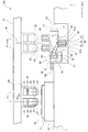
- a flip chip bonding apparatus 100 that is an electronic component mounting apparatus on which an electronic component handling unit 30 according to an embodiment of the present invention is mounted will be described with reference to FIG.
- the flip chip bonding apparatus 100 includes a gantry 11, a mounting stage 15, a gantry frame 13 that extends in the Y direction across the mounting stage 15, and moves in the X direction.
- a mounting head 20 that is attached and moves in the Y direction, a mounting nozzle 26 that is attached to the mounting head 20 and moves the mounting tool 23 in the Z direction, a wafer holder 50, and an electronic device that picks up, reverses, and delivers the semiconductor chip 18
- a component handling unit 30 and a control unit 60 for controlling the operation of each unit are provided.
- the direction in which the gantry frame 13 extends will be described as the Y direction, the direction orthogonal thereto as the X direction, and the vertical direction perpendicular to the XY plane as the Z direction.
- the mounting stage 15 vacuum-sucks a circuit board 17 on which a semiconductor chip 18 as an electronic component is mounted on the surface, and heats the circuit board 17 adsorbed on the surface by a heater (not shown) provided inside.
- the mounting stage 15 is fixed to the gantry 11.
- the mounting stage 15 is connected to a transport rail 16 that transports the circuit board 17 from the board supply unit (not shown) onto the mounting stage 15 and sends the circuit board 17 on which the semiconductor chip 18 has been mounted to a product stock (not shown). ing.
- the gantry frame 13 is a portal frame, and its legs are fixed on a slider 14 that slides in the X direction on two guide rails 12 that are fixed on the frame 11 and extend in the X direction. Since the slider 14 is moved in the X direction by an X direction drive motor (not shown), the gantry frame 13 is moved in the X direction by the X direction drive motor.
- the mounting head 20 is attached to the gantry frame 13 and moved in the Y direction by a Y direction drive motor (not shown).
- a Y direction drive motor (not shown).
- the mounting head 20 is moved in the X direction together with the gantry frame 13, so that the mounting head 20 is moved in the horizontal direction (XY direction) by the X direction drive motor and the Y direction drive motor.
- Two mounting nozzles 26 are attached to the mounting head 20 side by side at a pitch P1 in the Y direction.
- the mounting nozzle 26 drives the base portion 22 in the Z direction according to the rotation of the motor 21, the base portion 22 attached to the mounting head 20 so as to be movable in the Z direction, and the motor 21 fixed to the mounting head 20.
- a ball screw 24 and a pulse heater 25 attached to the lower side of the base portion 22 are included.
- a mounting tool 23 for adsorbing the semiconductor chip 18 and thermocompression bonding the semiconductor chip 18 to the circuit board 17 is attached to the lower side of the pulse heater 25.
- a vacuum hole for vacuum-sucking the semiconductor chip 18 is provided in the center of the mounting tool 23.
- the pitch P1 of the two mounting nozzles 26 is the same as the pitch P2 of the two pickup nozzles 42 mounted on the electronic component handling unit 30 described later.
- the mounting head 20 is movable in the XY directions, in the following description, when the mounting head 20 moves in the Y direction, the center of the mounting tool 23 is above the one-dot chain line 48 shown in FIG. It will be described as moving.
- the wafer holder 50 is an annular member that holds the diced wafer 51. As shown in FIG. 1, the wafer holder 50 is moved in the Y direction by a Y direction drive motor (not shown). Further, a push-up unit 55 that pushes up the semiconductor chip 18 of the wafer 51 upward is disposed below the wafer holder 50. The push-up unit 55 is moved in the X direction by an X direction drive motor (not shown).
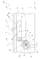
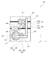
- the electronic component handling unit 30 includes a guide rail 38 fixed to the groove 19 extending in the X direction of the gantry 11, a slider 37 that is guided by the guide rail 38 and moves in the X direction, A main body 31 fixed to the slider 37 and moving in the X direction together with the slider 37, a rotary shaft 32 attached to the main body 31, a rotary shaft 32 attached to the rotary shaft 32, and obliquely downward in the Z direction from the center line 35 of the rotary shaft 32.
- a mounting arm 33 that extends, a flip head 40 that is fixed to the tip of the mounting arm 33 with a bolt 34, and a stepping motor 36 that is a reverse driving mechanism that rotates the rotating shaft 32 to reverse the flip head 40 are provided.
- the guide rail 38 has a stator and the slider 37 has a mover
- the guide rail 38 and the slider 37 constitute an X-direction linear motor 39 that is a linear drive mechanism that drives the main body 31 in the X direction. To do.
- the flip head 40 includes a base 41 and two pickup nozzles 42 attached to the lower surface 41 b of the base 41 in the Z direction.
- the base 41 is a plate-like member fixed to the tip of the mounting arm 33 with a bolt 34, and the two pickup nozzles 42 are linearly spaced in the X direction with a pitch P2 with respect to the center line 49 in the Z direction of the flip head 40. It is being fixed to the lower surface 41b of the base 41 so that it may rank.
- the flip head 40 indicated by a solid line shows a case where the pickup nozzle 42 faces downward (a state in which the upper surface 41 a of the base 41 can be seen), and the flip head 40 indicated by an alternate long and short dash line is inverted.
- the lower surface 41b is upward in the Z direction and the pickup nozzle 42 is also upward.
- an alternate long and short dash line 47 indicates the arrangement direction of the two pickup nozzles 42 when the pickup nozzle 42 faces downward.
- the arrangement direction of the pickup nozzles 42 (direction in which the one-dot chain line 47 extends) is inclined by 45 ° from the center line 35 (direction in which the rotation shaft 32 extends) of the rotation shaft 32 toward the X-axis direction. Yes.
- the two pickup nozzles 42 are moved in the X direction on the alternate long and short dash line 47.
- the direction in which the alternate long and short dash line 47 extends is the X direction and the main body 31 moves in the X direction
- the direction in which the rotating shaft 32 extends is also inclined by 45 ° with respect to the moving direction of the main body 31.
- the mounting arm 33 extends from the center line 35 of the rotating shaft 32 in a downward direction in the Z direction, and the base 41 is fixed to the tip of the mounting arm 33 with a bolt 34.
- the upper surface 41a of the base 41 is at a position lower than the center (center line 35) of the rotation shaft 32 by the height H1.
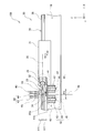
- the pickup nozzle 42 includes a cylindrical casing 43 provided with a hole extending in the longitudinal direction in the center, and a pickup tool 44 that moves in the longitudinal direction in the hole provided in the casing 43.
- An electromagnetic coil 45 is provided in the casing 43, and the feeding amount of the pickup tool 44 from the end surface of the casing 43 can be changed by energizing the electromagnetic coil 45.
- the pickup tool 44 is provided with a vacuum hole in the center, and the semiconductor chip 18 can be vacuum-sucked to the tip surface.
- the arrangement direction of the pickup tools 44 rotates 90 ° from the X direction to the Y direction.
- the upper surface 41 a of the base 41 to which the mounting arm 33 is fixed is positioned higher than the center line 35 of the rotating shaft 32 by the height H ⁇ b> 1.
- the flip head 40 when the flip head 40 is reversed, the distance between the pickup tool 44 and the mounting tool 23 is shortened, and the semiconductor chip 18 described later is received by the mounting tool 23 from the pickup tool 44.
- the feeding amount of the pick-up tool 44 when passing is small.
- the motor 21, the stepping motor 36, the X-direction drive motor, the Y-direction drive motor, and the like of the flip chip bonding apparatus 100 configured as described above are all controlled by the control unit 60.
- the control unit 60 is a computer including a CPU that performs arithmetic processing therein and a storage unit that stores operation programs and operation data.
- the operation of the flip chip bonding apparatus 100 will be described with reference to FIGS.
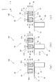
- the controller 60 moves the pick-up tool 44 over the wafer holder 50 by the X-direction linear motor 39 with the pick-up tool 44 facing downward as shown by solid lines in FIGS. Then, as shown in FIG. 5A, the control unit 60 adjusts the position so that the center position of one pickup nozzle 42 is directly above the semiconductor chip 18 to be picked up. Further, the control unit 60 adjusts the position so that the position of the push-up unit 55 is directly below the semiconductor chip 18 to be picked up.
- the control unit 60 energizes the electromagnetic coil 45 of the pickup nozzle 42 to feed the tip surface of the pickup tool 44 downward, and at the same time, pushes up the semiconductor chip 18 from below the dicing sheet 52 by the push-up unit 55. Further, the control unit 60 connects a vacuum device (not shown) and the pickup tool 44 so that the vacuum hole of the pickup tool 44 is evacuated. Then, the semiconductor chip 18 pushed up by the push-up unit 55 and in contact with the front end surface of the pickup tool 44 comes into contact with the front end surface of the pickup tool 44 and is vacuum-sucked to the front end surface of the pickup tool 44. Once the semiconductor chip 18 is picked up by the pickup tool 44, the control unit 60 controls the energization current of the electromagnetic coil 45 until the semiconductor chip 18 comes close to the end face of the casing 43 as shown in FIG. Retract the tip of 44.
- the control unit 60 drives the X-direction linear motor 39 shown in FIG. 3 to move the flip head 40 in the X direction, and the position of another pickup tool 44 is moved.
- the position is adjusted so that it is directly above the semiconductor chip 18 to be picked up and the position of the push-up unit 55 is directly below the semiconductor chip 18 to be picked up next.
- the controller 60 energizes the electromagnetic coil 45 of the pickup nozzle 42 to cause the pickup tool 44 to protrude downward, and at the same time, the semiconductor chip 18 is pushed up from below the dicing sheet 52 by the push-up unit 55. Then, the next semiconductor chip 18 is vacuum-sucked to the front end surface of the pickup tool 44.
- control unit 60 controls the energization current of the electromagnetic coil 45 until the semiconductor chip 18 comes close to the end face of the casing 43 as shown in FIG. The front end surface of the pickup tool 44 is retracted.
- the control unit 60 When the control unit 60 picks up the two semiconductor chips 18 with the two pickup nozzles 42, the control unit 60 moves the electronic component handling unit 30 in the X direction by the X-direction linear motor 39 shown in FIG. Accordingly, as shown in FIGS. 5C and 6A, the two pickup nozzles 42 that vacuum-suck the semiconductor chip 18 also move in the X direction. At this time, the two pickup nozzles 42 of the flip head 40 move in the X direction on the alternate long and short dash line 47 as described with reference to FIG.
- the control unit 60 moves the flip head 40 to the inversion position, as described above, the stepping motor 36 shown in FIGS. 3 and 4 rotates the rotary shaft 32 by 180 ° to invert the flip head 40. Then, as described above with reference to FIGS. 3 and 4, the base 41 is reversed and the two pickup nozzles 42 are directed upward.
- the arrangement direction of the two pickup nozzles 42 is the Y direction rotated by 90 ° from the X direction before reversal. 6B is a line indicating the arrangement direction of the two pickup nozzles 42 after the flip head 40 is reversed, and the center of the two mounting tools 23 when the two mounting tools 23 move in the Y direction. It is also a line that moves in the Y direction.
- the control unit 60 operates the Y-direction drive motor as shown in FIG. 2 to move the mounting head 20 directly above the inverted flip head 40.
- the centers of the two mounting tools 23 move in the Y direction along the alternate long and short dash line 48 shown in FIGS.
- the pitch P1 of the two mounting nozzles 26 is the same as the pitch P2 of the two pickup nozzles 42, when the mounting head 20 comes directly above the inverted pickup nozzle 42, it is shown in FIG.
- the center positions of the two mounting tools 23 and the center positions of the two pickup tools 44 coincide with each other.
- the control unit 60 energizes each electromagnetic coil 45 of each pickup nozzle 42 to feed the tip end surface of the pickup tool 44 as shown in FIG.
- the semiconductor chip 18 adsorbed on the front end surface of the pickup tool 44 comes close to the surface of the mounting tool 23.
- the control part 60 cancels
- the semiconductor chip 18 is vacuum-sucked on the surface of each mounting tool 23 away from the tip surface of each pickup tool 44. In this way, the semiconductor chip 18 is delivered from the two pickup tools 44 to the two mounting tools 23.
- the control unit 60 delivers the semiconductor chip 18 from the two pickup tools 44 to the two mounting tools 23
- the current of the electromagnetic coil 45 of the pickup nozzle 42 is adjusted and the tip surface of the pickup tool 44 is pulled back to the original state to perform stepping.
- the motor 36 is rotated 180 ° in the opposite direction to that during reversal, and the flip head 40 is returned to the original state (the state where it is not reversed) with the pickup nozzle 42 facing downward.
- the control unit 60 moves the mounting head 20 onto the circuit board 17 by a Y-direction drive motor (not shown) as shown in FIG. 7C. Then, the semiconductor chip 18 that is vacuum-sucked by the mounting tool 23 is heated by the pulse heater 25 of the mounting nozzle 26, the motor 21 is rotated, and the mounting tool 23 is lowered onto the circuit board 17 together with the base portion 22, so that mounting is performed.
- the semiconductor chip 18 is thermocompression bonded onto the circuit board 17 by the tool 23.
- the thermocompression bonding of the semiconductor chips 18 may be performed one by one or two semiconductor chips 18 may be simultaneously thermocompression bonded to the circuit board 17.
- the plurality of pickup nozzles 42 are arranged so as to be inclined by 45 ° with respect to the direction in which the rotation shaft 32 extends. By rotating, it is possible to simultaneously invert the picked-up semiconductor chip 18 and change the arrangement direction of the semiconductor chips 18 by 90 °. For this reason, by using the electronic component handling unit 30 of this embodiment, the arrangement direction of the mounting tool 23 of the flip chip bonding apparatus 100 and the arrangement direction of the pickup nozzle 42 are shifted by 90 ° with a simple structure and the installation area is small. The flip chip bonding apparatus 100 can be obtained.
- the two pickup nozzles 42 are attached to the flip head 40.
- the pickup heads are arranged in a straight line, three or more pickup nozzles 42 are attached to the flip head 40. Also good.
- the number of mounting nozzles 26 arranged in the mounting head 20 may be three or more instead of two as long as they are arranged in parallel. Further, the number of pickup nozzles 42 may be larger than the number of mounting nozzles 26.
- 11 mounts, 12 guide rails, 13 gantry frames, 14 sliders, 15 mounting stages, 16 transport rails, 17,912 circuit boards, 18,910 semiconductor chips, 19 grooves, 20 mounting heads, 21 motors, 22 base units, 23 mountings Tool, 24 ball screw, 25 pulse heater, 26 mounting nozzle, 30 electronic component handling unit, 31 body, 32 rotating shaft, 33 mounting arm, 34 bolt, 35, 49 center line, 36 stepping motor, 37 slider, 38 guide rail 39, X direction linear motor, 40 flip head, 41 base, 42 pickup nozzle, 43 casing, 44, 905 pickup tool, 45 electromagnetic coil, 47, 48 dash-dot line, 50 wafer Holder, 51,911 wafer, 52 dicing sheet, 55,909 push-up unit, 60 control unit, 100,900,950 flip chip bonding apparatus, 901 chip supply unit, 902 pickup unit, 902a pickup head, 903,953 reversing mechanism, 904 bonding unit, 904a bonding head, 906 bonding tool, 907 Y direction drive mechanism, 90
Priority Applications (4)
| Application Number | Priority Date | Filing Date | Title |
|---|---|---|---|
| JP2017560056A JP6513226B2 (ja) | 2016-01-06 | 2016-11-29 | 電子部品ハンドリングユニット |
| CN201680082710.0A CN108701620B (zh) | 2016-01-06 | 2016-11-29 | 电子零件处理单元 |
| KR1020187022087A KR102079082B1 (ko) | 2016-01-06 | 2016-11-29 | 전자 부품 핸들링 유닛 |
| US16/068,360 US10497590B2 (en) | 2016-01-06 | 2016-11-29 | Electronic component handling unit |
Applications Claiming Priority (2)
| Application Number | Priority Date | Filing Date | Title |
|---|---|---|---|
| JP2016-001043 | 2016-01-06 | ||
| JP2016001043 | 2016-01-06 |
Publications (1)
| Publication Number | Publication Date |
|---|---|
| WO2017119216A1 true WO2017119216A1 (ja) | 2017-07-13 |
Family
ID=59274170
Family Applications (1)
| Application Number | Title | Priority Date | Filing Date |
|---|---|---|---|
| PCT/JP2016/085287 WO2017119216A1 (ja) | 2016-01-06 | 2016-11-29 | 電子部品ハンドリングユニット |
Country Status (6)
| Country | Link |
|---|---|
| US (1) | US10497590B2 (ko) |
| JP (1) | JP6513226B2 (ko) |
| KR (1) | KR102079082B1 (ko) |
| CN (1) | CN108701620B (ko) |
| TW (1) | TWI632626B (ko) |
| WO (1) | WO2017119216A1 (ko) |
Cited By (4)
| Publication number | Priority date | Publication date | Assignee | Title |
|---|---|---|---|---|
| JPWO2019044819A1 (ja) * | 2017-08-28 | 2020-07-09 | 株式会社新川 | 対象物に対して移動体を直線移動させる装置および方法 |
| JPWO2019044816A1 (ja) * | 2017-08-28 | 2020-07-30 | 株式会社新川 | 対象物に対して第1移動体及び第2移動体を直線移動させる装置及び方法 |
| KR20210144899A (ko) | 2019-04-15 | 2021-11-30 | 가부시키가이샤 신가와 | 실장 장치 |
| WO2022195693A1 (ja) * | 2021-03-16 | 2022-09-22 | 株式会社新川 | 搬送装置、搬送方法、および、プログラム |
Families Citing this family (4)
| Publication number | Priority date | Publication date | Assignee | Title |
|---|---|---|---|---|
| TWI734434B (zh) * | 2019-04-11 | 2021-07-21 | 日商新川股份有限公司 | 接合裝置 |
| US11972968B2 (en) * | 2020-07-02 | 2024-04-30 | Sharpack Technology Pte. Ltd. | Fluxless gang die bonding arrangement |
| CN114951879A (zh) * | 2022-06-08 | 2022-08-30 | 希诺股份有限公司 | 一种真空保温杯低温高效抽真空密封设备及密封工艺 |
| US20240107735A1 (en) * | 2022-09-27 | 2024-03-28 | Canon Kabushiki Kaisha | Apparatus including a plurality of heads and a method of using the same |
Citations (2)
| Publication number | Priority date | Publication date | Assignee | Title |
|---|---|---|---|---|
| JPH1167879A (ja) * | 1997-08-26 | 1999-03-09 | Matsushita Electric Works Ltd | 半導体実装方法及びその装置 |
| JP2012023230A (ja) * | 2010-07-15 | 2012-02-02 | Yamaha Motor Co Ltd | 実装機 |
Family Cites Families (21)
| Publication number | Priority date | Publication date | Assignee | Title |
|---|---|---|---|---|
| JPS4840862B1 (ko) | 1970-11-02 | 1973-12-03 | ||
| JPS4840862A (ko) | 1971-09-23 | 1973-06-15 | ||
| US4322198A (en) * | 1980-04-16 | 1982-03-30 | Northern Telecom Limited | Coil handling device |
| KR920022482A (ko) * | 1991-05-09 | 1992-12-19 | 가나이 쯔도무 | 전자부품 탑재모듈 |
| JPH06120465A (ja) * | 1992-10-06 | 1994-04-28 | Matsushita Electric Ind Co Ltd | 実装装置 |
| US5507614A (en) * | 1995-03-02 | 1996-04-16 | Cybeq Systems | Holder mechanism for simultaneously tilting and rotating a wafer cassette |
| DE19905958C1 (de) * | 1999-02-12 | 2000-06-21 | Siemens Ag | Vorrichtung zum Bestücken von Substraten mit elektrischen Bauelementen mittels mehrerer unabhängiger Handhabungsssyteme |
| JP3636127B2 (ja) * | 2001-10-12 | 2005-04-06 | 松下電器産業株式会社 | 電子部品実装装置および電子部品実装方法 |
| SG104292A1 (en) * | 2002-01-07 | 2004-06-21 | Advance Systems Automation Ltd | Flip chip bonder and method therefor |
| US6506614B1 (en) * | 2002-01-29 | 2003-01-14 | Tyco Electronics Corporation | Method of locating and placing eye point features of a semiconductor die on a substrate |
| JP2004103923A (ja) * | 2002-09-11 | 2004-04-02 | Tdk Corp | 電子部品の実装装置および実装方法 |
| JP3879679B2 (ja) * | 2003-02-25 | 2007-02-14 | 松下電器産業株式会社 | 電子部品搭載装置および電子部品搭載方法 |
| JP4672384B2 (ja) * | 2004-04-27 | 2011-04-20 | 大日本印刷株式会社 | Icタグ付シートの製造方法、icタグ付シートの製造装置、icタグ付シート、icチップの固定方法、icチップの固定装置、およびicタグ |
| JP2007158052A (ja) | 2005-12-06 | 2007-06-21 | Matsushita Electric Ind Co Ltd | 電子部品実装装置及び実装エラー修復方法 |
| JP4840862B2 (ja) | 2006-08-29 | 2011-12-21 | 東レエンジニアリング株式会社 | 実装装置のチップ供給方法、及びその実装装置 |
| CH698718B1 (de) * | 2007-01-31 | 2009-10-15 | Oerlikon Assembly Equipment Ag | Vorrichtung für die Montage eines Flipchips auf einem Substrat. |
| KR20100012257A (ko) * | 2008-07-28 | 2010-02-08 | 주식회사 탑 엔지니어링 | 칩 픽업장치 |
| KR101308467B1 (ko) * | 2009-08-04 | 2013-09-16 | 엘지디스플레이 주식회사 | 전자 부품 실장 장치 및 방법 |
| DE102010054360B4 (de) * | 2010-12-13 | 2018-09-20 | Leica Biosystems Nussloch Gmbh | Vorrichtung, Rackwendermodul, System und Verfahren zum Wenden von Racks |
| WO2015038074A1 (en) * | 2013-09-13 | 2015-03-19 | Orion Systems Integration Pte Ltd | System and method for positioning a semiconductor chip with a bond head, thermal bonding system and method |
| JP6211359B2 (ja) | 2013-09-18 | 2017-10-11 | ファスフォードテクノロジ株式会社 | フリップチップボンダ及びボンディング方法 |
-
2016
- 2016-11-15 TW TW105137225A patent/TWI632626B/zh active
- 2016-11-29 KR KR1020187022087A patent/KR102079082B1/ko active IP Right Grant
- 2016-11-29 CN CN201680082710.0A patent/CN108701620B/zh active Active
- 2016-11-29 JP JP2017560056A patent/JP6513226B2/ja active Active
- 2016-11-29 US US16/068,360 patent/US10497590B2/en active Active
- 2016-11-29 WO PCT/JP2016/085287 patent/WO2017119216A1/ja active Application Filing
Patent Citations (2)
| Publication number | Priority date | Publication date | Assignee | Title |
|---|---|---|---|---|
| JPH1167879A (ja) * | 1997-08-26 | 1999-03-09 | Matsushita Electric Works Ltd | 半導体実装方法及びその装置 |
| JP2012023230A (ja) * | 2010-07-15 | 2012-02-02 | Yamaha Motor Co Ltd | 実装機 |
Cited By (5)
| Publication number | Priority date | Publication date | Assignee | Title |
|---|---|---|---|---|
| JPWO2019044819A1 (ja) * | 2017-08-28 | 2020-07-09 | 株式会社新川 | 対象物に対して移動体を直線移動させる装置および方法 |
| JPWO2019044816A1 (ja) * | 2017-08-28 | 2020-07-30 | 株式会社新川 | 対象物に対して第1移動体及び第2移動体を直線移動させる装置及び方法 |
| JP7072264B2 (ja) | 2017-08-28 | 2022-05-20 | 株式会社新川 | 対象物に対して移動体を直線移動させる装置および方法 |
| KR20210144899A (ko) | 2019-04-15 | 2021-11-30 | 가부시키가이샤 신가와 | 실장 장치 |
| WO2022195693A1 (ja) * | 2021-03-16 | 2022-09-22 | 株式会社新川 | 搬送装置、搬送方法、および、プログラム |
Also Published As
| Publication number | Publication date |
|---|---|
| CN108701620B (zh) | 2021-06-29 |
| KR20180100363A (ko) | 2018-09-10 |
| CN108701620A (zh) | 2018-10-23 |
| JP6513226B2 (ja) | 2019-05-15 |
| TWI632626B (zh) | 2018-08-11 |
| US20190006211A1 (en) | 2019-01-03 |
| KR102079082B1 (ko) | 2020-02-19 |
| TW201730993A (zh) | 2017-09-01 |
| JPWO2017119216A1 (ja) | 2018-10-25 |
| US10497590B2 (en) | 2019-12-03 |
Similar Documents
| Publication | Publication Date | Title |
|---|---|---|
| JP6573289B2 (ja) | 電子部品実装装置 | |
| WO2017119216A1 (ja) | 電子部品ハンドリングユニット | |
| KR101977987B1 (ko) | 다이 본더 및 본딩 방법 | |
| JP4308772B2 (ja) | 部品供給ヘッド装置、部品供給装置、部品実装装置、及び実装ヘッド部の移動方法 | |
| KR101082827B1 (ko) | 비전카메라 일체형 픽업유닛을 구비하는 플립칩 장착 장치 | |
| JP5507775B1 (ja) | ボンディング装置およびボンディング方法 | |
| JP3497078B2 (ja) | ダイボンダ | |
| JP2012186505A (ja) | 部品供給装置 | |
| KR20140146852A (ko) | 플립칩 마운터 및 이를 이용한 마운팅 방법 | |
| JP5078424B2 (ja) | 電子部品の実装装置 | |
| JP2019149399A (ja) | ボンディング装置 | |
| JP2009070976A (ja) | 部品実装装置 | |
| JP2007324623A (ja) | 電子部品実装方法 | |
| JP2009252890A (ja) | 部品供給装置 | |
| JP4602838B2 (ja) | 半導体チップの実装装置 | |
| JP5479961B2 (ja) | 電子部品の実装装置及び実装方法 | |
| JP2013251322A (ja) | 部品移載装置および部品移戴方法 | |
| JP4969977B2 (ja) | 部品実装装置 | |
| JP4925762B2 (ja) | 部品実装装置 |
Legal Events
| Date | Code | Title | Description |
|---|---|---|---|
| 121 | Ep: the epo has been informed by wipo that ep was designated in this application |
Ref document number: 16883716 Country of ref document: EP Kind code of ref document: A1 |
|
| WWE | Wipo information: entry into national phase |
Ref document number: 2017560056 Country of ref document: JP |
|
| NENP | Non-entry into the national phase |
Ref country code: DE |
|
| ENP | Entry into the national phase |
Ref document number: 20187022087 Country of ref document: KR Kind code of ref document: A |
|
| 122 | Ep: pct application non-entry in european phase |
Ref document number: 16883716 Country of ref document: EP Kind code of ref document: A1 |