WO2017119083A1 - 半導体デバイスの載置台及び車載装置 - Google Patents
半導体デバイスの載置台及び車載装置 Download PDFInfo
- Publication number
- WO2017119083A1 WO2017119083A1 PCT/JP2016/050259 JP2016050259W WO2017119083A1 WO 2017119083 A1 WO2017119083 A1 WO 2017119083A1 JP 2016050259 W JP2016050259 W JP 2016050259W WO 2017119083 A1 WO2017119083 A1 WO 2017119083A1
- Authority
- WO
- WIPO (PCT)
- Prior art keywords
- semiconductor device
- fixing
- mounting table
- support
- surface portion
- Prior art date
- Legal status (The legal status is an assumption and is not a legal conclusion. Google has not performed a legal analysis and makes no representation as to the accuracy of the status listed.)
- Ceased
Links
Images




Classifications
-
- H—ELECTRICITY
- H10—SEMICONDUCTOR DEVICES; ELECTRIC SOLID-STATE DEVICES NOT OTHERWISE PROVIDED FOR
- H10W—GENERIC PACKAGES, INTERCONNECTIONS, CONNECTORS OR OTHER CONSTRUCTIONAL DETAILS OF DEVICES COVERED BY CLASS H10
- H10W40/00—Arrangements for thermal protection or thermal control
- H10W40/60—Securing means for detachable heating or cooling arrangements, e.g. clamps
- H10W40/611—Bolts or screws
-
- H—ELECTRICITY
- H10—SEMICONDUCTOR DEVICES; ELECTRIC SOLID-STATE DEVICES NOT OTHERWISE PROVIDED FOR
- H10W—GENERIC PACKAGES, INTERCONNECTIONS, CONNECTORS OR OTHER CONSTRUCTIONAL DETAILS OF DEVICES COVERED BY CLASS H10
- H10W40/00—Arrangements for thermal protection or thermal control
- H10W40/20—Arrangements for cooling
- H10W40/22—Arrangements for cooling characterised by their shape, e.g. having conical or cylindrical projections
-
- H—ELECTRICITY
- H10—SEMICONDUCTOR DEVICES; ELECTRIC SOLID-STATE DEVICES NOT OTHERWISE PROVIDED FOR
- H10W—GENERIC PACKAGES, INTERCONNECTIONS, CONNECTORS OR OTHER CONSTRUCTIONAL DETAILS OF DEVICES COVERED BY CLASS H10
- H10W40/00—Arrangements for thermal protection or thermal control
- H10W40/70—Fillings or auxiliary members in containers or in encapsulations for thermal protection or control
-
- B—PERFORMING OPERATIONS; TRANSPORTING
- B60—VEHICLES IN GENERAL
- B60R—VEHICLES, VEHICLE FITTINGS, OR VEHICLE PARTS, NOT OTHERWISE PROVIDED FOR
- B60R16/00—Electric or fluid circuits specially adapted for vehicles and not otherwise provided for; Arrangement of elements of electric or fluid circuits specially adapted for vehicles and not otherwise provided for
- B60R16/02—Electric or fluid circuits specially adapted for vehicles and not otherwise provided for; Arrangement of elements of electric or fluid circuits specially adapted for vehicles and not otherwise provided for electric constitutive elements
- B60R16/03—Electric or fluid circuits specially adapted for vehicles and not otherwise provided for; Arrangement of elements of electric or fluid circuits specially adapted for vehicles and not otherwise provided for electric constitutive elements for supply of electrical power to vehicle subsystems or for
-
- H—ELECTRICITY
- H10—SEMICONDUCTOR DEVICES; ELECTRIC SOLID-STATE DEVICES NOT OTHERWISE PROVIDED FOR
- H10W—GENERIC PACKAGES, INTERCONNECTIONS, CONNECTORS OR OTHER CONSTRUCTIONAL DETAILS OF DEVICES COVERED BY CLASS H10
- H10W40/00—Arrangements for thermal protection or thermal control
- H10W40/20—Arrangements for cooling
- H10W40/231—Arrangements for cooling characterised by their places of attachment or cooling paths
- H10W40/242—Arrangements for cooling characterised by their places of attachment or cooling paths comprising thermal conductors between chips and the and the arrangements for cooling, e.g. compliant heat-spreaders
-
- H—ELECTRICITY
- H10—SEMICONDUCTOR DEVICES; ELECTRIC SOLID-STATE DEVICES NOT OTHERWISE PROVIDED FOR
- H10W—GENERIC PACKAGES, INTERCONNECTIONS, CONNECTORS OR OTHER CONSTRUCTIONAL DETAILS OF DEVICES COVERED BY CLASS H10
- H10W40/00—Arrangements for thermal protection or thermal control
- H10W40/60—Securing means for detachable heating or cooling arrangements, e.g. clamps
-
- H—ELECTRICITY
- H10—SEMICONDUCTOR DEVICES; ELECTRIC SOLID-STATE DEVICES NOT OTHERWISE PROVIDED FOR
- H10W—GENERIC PACKAGES, INTERCONNECTIONS, CONNECTORS OR OTHER CONSTRUCTIONAL DETAILS OF DEVICES COVERED BY CLASS H10
- H10W72/00—Interconnections or connectors in packages
- H10W72/90—Bond pads, in general
- H10W72/931—Shapes of bond pads
Definitions
- the present invention relates to a semiconductor device mounting table and an in-vehicle device.
- a semiconductor device covered with a mold resin is placed in a metal casing having a heat radiating portion such as a fin (see, for example, JP 2010-10505 A).
- a mounting table is provided in the housing, and a semiconductor device is mounted on the mounting table.
- the semiconductor device mounted on the mounting table is fixed to the fixing portion by a fastening member or the like. Inconvenience may occur because the fixed semiconductor device is warped or the surface of the mounting table is warped.
- the present invention provides a semiconductor device mounting table and an in-vehicle device capable of eliminating the disadvantages caused by warping of a semiconductor device fixed to a fixed part or warping of the surface of the mounting table.
- the semiconductor device mounting table comprises: A main body portion on which a semiconductor device is placed, the support portion supporting at least a part of a peripheral edge portion of the semiconductor device, and being located on the inner peripheral side of the support portion and having a height lower than that of the support portion.
- the semiconductor device is substantially rectangular when viewed from above,
- the support portion may support four sides of the semiconductor device.
- the fixing portion has two fixing holes for inserting and fixing a fastening member for fastening the semiconductor device,
- the two fixing holes may be provided on a diagonal line.
- the support part is substantially rectangular when viewed from above, and has a first support part and a second support part protruding to the inner peripheral side, The first support part and the second support part may be provided diagonally.
- the fixing portion has two fixing holes for inserting and fixing a fastening member for fastening the semiconductor device,
- the fixing hole may be provided in each of the first support part and the second support part.
- a heat dissipation material may be placed on the bottom surface.
- the heat dissipation material may be a heat dissipation agent having viscosity.
- a groove part deeper than the bottom face part may be provided so as to surround the bottom face part intermittently or continuously.
- the bottom surface portion and the groove portion may be provided adjacent to each other.
- the fixing portion has at least a fixing hole for inserting and fixing a fastening member for fastening the semiconductor device,
- the groove portion may be provided between the bottom surface portion and the fixing hole.
- the in-vehicle device is A semiconductor device; A mounting table having a main body portion on which the semiconductor device is mounted; and a fixing portion for fixing the semiconductor device to the main body portion;
- the main body has a support part that supports at least a part of the peripheral part of the semiconductor device, and a bottom part that is located on the inner peripheral side of the support part and has a lower height than the support part.
- the fixing part is provided on the support part,
- the height difference ⁇ H between the support portion and the bottom portion is the maximum warp H1 to the upper side of the calculated or measured bottom surface portion and the maximum warpage to the lower side of the bottom surface of the calculated or measured semiconductor device. It is larger than the sum of H2 (H1 + H2).
- the difference ⁇ H in height between the support portion and the bottom surface portion is calculated as the maximum warp H1 to the upper side of the bottom surface portion and to the lower side of the bottom surface of the semiconductor device as calculated or measured. Is larger than the sum (H1 + H2) of the maximum warpage H2. For this reason, even if the bottom surface portion is along the upper side or the bottom surface of the semiconductor device is along the lower side, the semiconductor device can be prevented from coming into contact with the bottom surface portion. For this reason, the inconvenience caused by warping of the semiconductor device fixed to the fixing portion or warping of the surface of the mounting table can be solved.
- FIG. 1 is an upper plan view of an in-vehicle device according to an embodiment of the present invention.
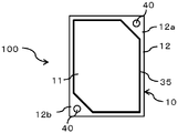
- FIG. 2 is an upper plan view of the semiconductor device mounting table according to the embodiment of the present invention.
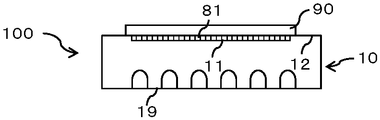
- FIG. 3 is an upper plan view showing a mode in which the semiconductor device is mounted on the mounting table according to the embodiment of the present invention.
- 4 is a cross-sectional view of FIG. 3 taken along line IV-IV of FIG.
- FIG. 5 is a cross-sectional view for explaining the height difference ⁇ H between the support portion and the bottom portion and the depth D of the groove portion in the embodiment of the present invention.
- FIG. 1 is an upper plan view of an in-vehicle device according to an embodiment of the present invention.
- FIG. 2 is an upper plan view of the semiconductor device mounting table according to the embodiment of the present invention.
- FIG. 3 is an upper plan view showing a mode in which the semiconductor device is mounted on the mounting table according to the embodiment of the present invention.
- 4 is a cross-sectional view of FIG
- FIG. 6 shows the maximum warpage H1 to the upper side of the calculated bottom surface portion and the maximum warpage H2 to the lower side of the bottom surface of the semiconductor device calculated or measured in the embodiment of the present invention. It is sectional drawing for demonstrating.
- FIG. 7 is a drawing corresponding to FIG. 4, and is a cross-sectional view when the semiconductor device is mounted on the mounting table according to the first modification of the embodiment of the present invention.
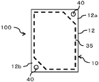
- FIG. 8 is an upper plan view of the semiconductor device mounting table according to the second modification of the embodiment of the present invention.
- FIG. 9 is an upper plan view of a semiconductor device mounting table according to the third modification of the embodiment of the present invention.
- Embodiment ⁇ Configuration The semiconductor device mounting table according to the present embodiment is disposed in an in-vehicle device such as a power supply device used in an automobile, for example.
- the power supply device is, for example, a metal pedestal 220 for mounting the switching power supply device, and, for example, a metal for electromagnetically shielding the switching power supply device by combining with the pedestal 220.
- a housing 200 having a cover 210 made of metal is included. Although the inside of the cover 210 is also illustrated in FIG. 1, the inside of the cover 210 is actually covered with the cover 210 and cannot be viewed from the outside.
- a mounting table 100 is provided in the housing 200.
- the mounting table 100 of the semiconductor device 90 includes a main body unit 10 on which the semiconductor device 90 is mounted, and a fixing unit 40 for fixing the semiconductor device 90 to the main body unit 10. ,have.
- the main body portion 10 is located on the inner peripheral side of the support portion 12 that supports at least a part of the peripheral portion of the semiconductor device 90 and is lower in height than the support portion 12.
- a bottom surface portion 11 As shown in FIG. 2, the fixing portion 40 is provided on the support portion 12.
- the height difference ⁇ H (see FIG. 5) between the support portion 12 and the bottom surface portion 11 is the calculated or measured maximum warp H1 (see FIG. 6) upward of the bottom surface portion 11 and the calculated or measured semiconductor. It is larger than the sum (H1 + H2) of the maximum warpage H2 (see FIG. 6) to the lower side of the bottom surface of the device 90.
- the height difference ⁇ H between the support part 12 and the bottom part 11 can be 0.15 mm to 0.30 mm, preferably 0.15 mm to 0.20 mm, and even more preferably. Can be 0.15 mm to 0.17 mm.
- the mounting table 100 may be made of a metal material.
- ⁇ H can be made larger than H1 + H2.
- the upper limit of ⁇ H is 0.30 mm.
- the upper limit of ⁇ H is preferably 0.20 mm, and more preferably 0.17 mm.
- the main body 10 of the present embodiment may be substantially rectangular when viewed from above.
- “upward” means the normal direction side of the mounting surface on which the semiconductor device 90 is mounted.
- the “substantially rectangular shape” in the present embodiment is sufficient if there are two opposing pairs of sides, and includes, for example, a form in which corners are rounded.
- the support unit 12 may support at least two sides of the semiconductor device 90 facing each other. Further, the support unit 12 may support four sides of the semiconductor device 90. In the present embodiment, description will be made using a mode in which the support portion 12 supports four sides of the semiconductor device 90.
- the semiconductor device 90 may have a through hole 91 into which the fastening member 95 is inserted.
- the substantially rectangular support part 12 may have a first support part 12a and a second support part 12b protruding to the inner peripheral side.
- the 1st support part 12a and the 2nd support part 12b may be provided on a diagonal (corner part).
- the fixing hole 40 may be provided in each of the 1st support part 12a and the 2nd support part 12b.
- the first support portion 12a and the second support portion 12b may be semicircular and protrude toward the inner peripheral side.
- FIG. 2 shows a mode in which the groove portion 35 is provided so as to continuously surround the bottom surface portion 11
- FIG. 8 shows a mode in which the groove portion 35 is provided so as to intermittently surround the bottom surface portion 11. It is shown.
- a heat radiating material such as the heat radiating agent 80 and the heat radiating sheet 81 may be placed on the bottom surface portion 11.
- FIG. 4 shows an aspect in which the heat radiation agent 80 is placed on the bottom surface portion 11, and
- FIG. 7 shows an aspect in which the heat radiation sheet 81 is placed on the bottom surface portion 11.
- the support portion 12 supports the semiconductor device 90 only at the periphery, and the support portion 12 for supporting the semiconductor device 90 on the inner peripheral side from the groove portion 35 may not be provided. Moreover, the bottom face part 11 and the groove part 35 may be provided adjacently (continuously) (see FIG. 4).
- fins 19 may be provided on the back side of the main body 10. According to such an aspect, heat dissipation can be improved.
- the height difference ⁇ H between the support portion 12 and the bottom surface portion 11 is the calculated or measured maximum warpage H1 to the upper side of the bottom surface portion 11, and the calculated or measured semiconductor device 90. Is larger than the sum (H1 + H2) of the maximum warpage H2 to the lower side of the bottom surface (see FIGS. 5 and 6). For this reason, even if the bottom surface portion 11 is along the upper side or the bottom surface of the semiconductor device 90 is along the lower side, the semiconductor device 90 can be prevented from coming into contact with the bottom surface portion 11. For this reason, the inconvenience due to warpage of the semiconductor device 90 fixed to the fixing portion 40 or warping of the surface of the mounting table 100 can be solved. As an example of this, the height difference ⁇ H between the support portion 12 and the bottom surface portion 11 can be set to 0.15 mm or more.
- ⁇ H 0.30 mm or less
- heat generated in the semiconductor device 90 by the heat radiating sheet 81 (see FIG. 7) or the heat radiating agent 80 (see FIG. 4) can be efficiently transmitted to the mounting table 100.
- ⁇ H 0.20 mm or less
- heat generated in the semiconductor device 90 by the heat dissipation sheet 81 or the heat dissipation agent 80 can be efficiently transmitted to the mounting table 100, and ⁇ H is set to 0.17 mm or less, for example.
- the heat generated in the semiconductor device 90 can be more efficiently transmitted to the mounting table 100 by the heat radiating sheet 81 and the heat radiating agent 80.
- the support unit 12 supports the semiconductor device 90 in a balanced manner. Can do. For this reason, ⁇ H can be close to a value designed in advance, and the inconvenience due to warpage of the semiconductor device 90 fixed to the fixing portion 40 or warping of the surface of the mounting table 100 can be eliminated.
- the heat radiating agent 80 is employed as the heat radiating material, the thickness of the heat radiating agent 80 can be made more uniform, and the heat generated in the semiconductor device 90 can be efficiently transmitted to the mounting table 100.
- the semiconductor device 90 when the semiconductor device 90 is substantially rectangular, the semiconductor device 90 is more balanced by the support portion 12 by adopting a mode in which the support portion 12 supports the opposing long sides of the semiconductor device 90. Can be supported.
- the “substantially rectangular shape” means that there are two pairs of opposing sides, and the two opposing pairs of sides are short and long sides, for example, the corners are rounded. Is also included. Note that the short sides do not have to have the same length, and one of the pair of short sides may be longer than the other. Moreover, even if it says a long side, it does not need to be the same length, and one of a pair of long sides may be longer than the other. However, the shorter side of the longer side needs to be longer than the longer side of the shorter side.
- the support unit 12 can support the semiconductor device 90 in a more balanced manner. it can. Therefore, ⁇ H can be made closer to a value designed in advance, and the inconvenience caused by warping of the semiconductor device 90 fixed to the fixing portion 40 or warping of the surface of the mounting table 100 can be more reliably eliminated. Can do.
- the heat radiating agent 80 is adopted as the heat radiating material, the thickness of the heat radiating agent 80 can be made more uniform, and the heat generated in the semiconductor device 90 can be efficiently transmitted to the mounting table 100.
- the semiconductor device 90 when the embodiment in which the two fixing holes 40 are provided on the diagonal line is adopted, it is excellent in that the semiconductor device 90 can be fixed to the mounting table 100 in a balanced manner.
- the difference in height between the support portion 12 and the bottom surface portion 11 can be made more uniform in the entire surface direction.
- the heat generated in the semiconductor device 90 can be efficiently transmitted to the mounting table 100.
- the thickness of the heat radiating agent 80 when the heat radiating agent 80 is adopted as the heat radiating material, the thickness of the heat radiating agent 80 can be made more uniform, which is beneficial in that the heat generated in the semiconductor device 90 can be efficiently transmitted to the mounting table 100. is there.
- the substantially rectangular support part 12 has the 1st support part 12a and the 2nd support part 12b which protruded to the inner peripheral side, and the 1st support part 12a and the 2nd support part
- the semiconductor device 90 can be firmly supported by the first support part 12a and the second support part 12b in the diagonal line having a long length.
- the length of the diagonal line becomes longer, even if the area for supporting the semiconductor device 90 by the first support portion 12a and the second support portion 12b provided at the corner portion is increased, the height is higher than that of the support portion 12.
- the low bottom part 11 can be provided widely. For this reason, the inconvenience caused by warping of the semiconductor device 90 fixed to the fixing portion 40 or warping of the surface of the mounting table 100 can be more reliably solved.
- the space between the bottom surface portion 11 and the bottom surface of the semiconductor device 90 is used.
- the gap can be filled with a highly heat-dissipating material, and the heat generated in the semiconductor device 90 can be efficiently transmitted to the mounting table 100.
- a heat dissipation agent 80 having viscosity such as heat dissipation grease rather than the heat dissipation sheet 81.
- the groove portion 35 is formed so as to surround the bottom surface portion 11 continuously (see FIG. 2) or intermittently (see FIG. 8) between the bottom surface portion 11 and the support portion 12. May be provided.
- the heat radiating agent 80 leaks more reliably to the outside. It is excellent in that it can be prevented.
- the depth D of the groove part 35 may be larger than the height difference ⁇ H between the support part 12 and the bottom part 11.
- the depth D of the groove 35 may be 4 to 10 times ⁇ H, and more specifically 5 to 7 times.
- the heat radiation agent 80 that has spread and spread on the bottom surface portion 11 can be poured into the groove portion 35 as it is.
- the depth D of the groove 35 10 times or less of ⁇ H, it is possible to prevent a gap from being formed between the heat dissipation agent 80 poured into the groove 35 and the bottom surface of the semiconductor device 90.
- the depth D of the groove 35 7 times or less of ⁇ H, it is possible to more reliably prevent a gap from being formed between the heat radiation agent 80 poured into the groove 35 and the bottom surface of the semiconductor device 90. For these reasons, the heat generated in the semiconductor device 90 can be efficiently transmitted to the mounting table 100 through the heat radiation agent 80 poured into the groove portion 35.
- the expanded heat dissipation agent 80 sandwiched between the back surface of the semiconductor device 90 and the bottom surface portion 11 is buried in the fixing hole 40. Can be prevented.
Landscapes
- Cooling Or The Like Of Semiconductors Or Solid State Devices (AREA)
- Casings For Electric Apparatus (AREA)
- Cooling Or The Like Of Electrical Apparatus (AREA)
- Dc-Dc Converters (AREA)
Abstract
Description
半導体デバイスが載置される本体部であって、前記半導体デバイスの少なくとも周縁部の一部を支持する支持部と、前記支持部の内周側に位置するとともに前記支持部よりも高さが低くなっている底面部とを有する本体部と、
前記支持部に設けられ、前記半導体デバイスを前記本体部に固定するための固定部と、
を備え、
前記支持部と前記底面部との高さの差ΔHが、算出又は計測された底面部の上方側への最大の反りH1と算出又は計測された半導体デバイスの底面の下方側への最大の反りH2との和(H1+H2)よりも大きくなっている。
前記半導体デバイスは上方から見たときに略矩形状となり、
前記支持部は、前記半導体デバイスの4辺を支持してもよい。
前記固定部は、半導体デバイスを締結する締結部材を挿入して固定するための2つの固定孔を有し、
前記2つの固定孔は、対角線上に設けられてもよい。
前記支持部は上方から見たときに略矩形状となり、内周側に突出した第一支持部及び第二支持部を有し、
前記第一支持部及び前記第二支持部は対角線上に設けられてもよい。
前記固定部は、前記半導体デバイスを締結する締結部材を挿入して固定するための2つの固定孔を有し、
前記第一支持部及び前記第二支持部の各々に前記固定孔が設けられてもよい。
前記底面部には、放熱材料が載置されてもよい。
前記放熱材料は粘性を有する放熱剤であってもよい。
前記底面部と前記支持部との間には、前記底面部を断続的又は連続的に取り囲むようにして、前記底面部よりも深さの深い溝部が設けられてもよい。
前記底面部と前記溝部とが隣接して設けられてもよい。
前記固定部は、半導体デバイスを締結する締結部材を挿入して固定するための少なくとも固定孔を有し、
前記溝部は、前記底面部と前記固定孔との間に設けられてもよい。
半導体デバイスと、
前記半導体デバイスが載置される本体部と、前記半導体デバイスを前記本体部に固定するための固定部と、を有する載置台と、
を備え、
前記本体部は、前記半導体デバイスの少なくとも周縁部の一部を支持する支持部と、前記支持部の内周側に位置するとともに前記支持部よりも高さが低くなっている底面部とを有し、
前記固定部は前記支持部に設けられ、
前記支持部と前記底面部との高さの差ΔHは、算出又は計測された底面部の上方側への最大の反りH1と算出又は計測された半導体デバイスの底面の下方側への最大の反りH2との和(H1+H2)よりも大きくなっている。
《構成》
本実施の形態による半導体デバイスの載置台は、例えば自動車で用いられる電源装置等の車載装置内に配置される。図1に示すように、電源装置は、例えば、スイッチング電源装置を載置するための例えば金属製の台座220と、その台座220と組み合わせることでスイッチング電源装置を電磁的に遮蔽するための例えば金属製のカバー210とを有する筐体200を含んでいる。図1ではカバー210内も図示しているが、実際にはカバー210内はカバー210で覆われるため外側から見ることはできない。図1に示すように、筐体200内に載置台100が設けられている。
次に、上述した構成からなる本実施の形態による作用・効果であって、まだ説明していないものについて説明する。
11 底面部
12 支持部
12a 第一支持部
12b 第二支持部
20 突出部
35 溝部
40 固定部
80 放熱剤
90 半導体デバイス
95 締結部材
100 載置台
200 筐体
Claims (11)
- 半導体デバイスが載置される本体部であって、前記半導体デバイスの少なくとも周縁部の一部を支持する支持部と、前記支持部の内周側に位置するとともに前記支持部よりも高さが低くなっている底面部とを有する本体部と、
前記支持部に設けられ、前記半導体デバイスを前記本体部に固定するための固定部と、
を備え、
前記支持部と前記底面部との高さの差ΔHは、算出又は計測された底面部の上方側への最大の反りH1と算出又は計測された半導体デバイスの底面の下方側への最大の反りH2との和(H1+H2)よりも大きくなっていることを特徴とする半導体デバイスの載置台。 - 前記半導体デバイスは上方から見たときに略矩形状となり、
前記支持部は、前記半導体デバイスの4辺を支持することを特徴とする請求項1に記載の半導体デバイスの載置台。 - 前記固定部は、半導体デバイスを締結する締結部材を挿入して固定するための2つの固定孔を有し、
前記2つの固定孔は、対角線上に設けられていることを特徴とする請求項1又は2のいずれかに記載の半導体デバイスの載置台。 - 前記支持部は上方から見たときに略矩形状となり、内周側に突出した第一支持部及び第二支持部を有し、
前記第一支持部及び前記第二支持部は対角線上に設けられていることを特徴とする請求項1乃至3のいずれか1項に記載の半導体デバイスの載置台。 - 前記固定部は、前記半導体デバイスを締結する締結部材を挿入して固定するための2つの固定孔を有し、
前記第一支持部及び前記第二支持部の各々に前記固定孔が設けられていることを特徴とする請求項4に記載の半導体デバイスの載置台。 - 前記底面部には、放熱材料が載置されることを特徴とする請求項1乃至5のいずれか1項に記載の半導体デバイスの載置台。
- 前記放熱材料は粘性を有する放熱剤であることを特徴とする請求項6に記載の半導体デバイスの載置台。
- 前記底面部と前記支持部との間には、前記底面部を断続的又は連続的に取り囲むようにして、前記底面部よりも深さの深い溝部が設けられていることを特徴とする請求項7に記載の半導体デバイスの載置台。
- 前記底面部と前記溝部とが隣接して設けられていることを特徴とする請求項8に記載の半導体デバイスの載置台。
- 前記固定部は、半導体デバイスを締結する締結部材を挿入して固定するための少なくとも固定孔を有し、
前記溝部は、前記底面部と前記固定孔との間に設けられていることを特徴とする請求項8又は9のいずれかに記載の半導体デバイスの載置台。 - 半導体デバイスと、
前記半導体デバイスが載置される本体部と、前記半導体デバイスを前記本体部に固定するための固定部と、を有する載置台と、
を備え、
前記本体部は、前記半導体デバイスの少なくとも周縁部の一部を支持する支持部と、前記支持部の内周側に位置するとともに前記支持部よりも高さが低くなっている底面部とを有し、
前記固定部は前記支持部に設けられ、
前記支持部と前記底面部との高さの差ΔHは、算出又は計測された底面部の上方側への最大の反りH1と算出又は計測された半導体デバイスの底面の下方側への最大の反りH2との和(H1+H2)よりも大きくなっていることを特徴とする車載装置。
Priority Applications (4)
| Application Number | Priority Date | Filing Date | Title |
|---|---|---|---|
| US15/545,083 US10090225B2 (en) | 2016-01-06 | 2016-01-06 | Placement base for semiconductor device and vehicle equipment |
| PCT/JP2016/050259 WO2017119083A1 (ja) | 2016-01-06 | 2016-01-06 | 半導体デバイスの載置台及び車載装置 |
| JP2017508114A JP6243574B2 (ja) | 2016-01-06 | 2016-01-06 | 半導体デバイスの載置台及び車載装置 |
| CN201680014400.5A CN107408542B (zh) | 2016-01-06 | 2016-01-06 | 半导体器件的载置台以及车载装置 |
Applications Claiming Priority (1)
| Application Number | Priority Date | Filing Date | Title |
|---|---|---|---|
| PCT/JP2016/050259 WO2017119083A1 (ja) | 2016-01-06 | 2016-01-06 | 半導体デバイスの載置台及び車載装置 |
Publications (1)
| Publication Number | Publication Date |
|---|---|
| WO2017119083A1 true WO2017119083A1 (ja) | 2017-07-13 |
Family
ID=59273482
Family Applications (1)
| Application Number | Title | Priority Date | Filing Date |
|---|---|---|---|
| PCT/JP2016/050259 Ceased WO2017119083A1 (ja) | 2016-01-06 | 2016-01-06 | 半導体デバイスの載置台及び車載装置 |
Country Status (4)
| Country | Link |
|---|---|
| US (1) | US10090225B2 (ja) |
| JP (1) | JP6243574B2 (ja) |
| CN (1) | CN107408542B (ja) |
| WO (1) | WO2017119083A1 (ja) |
Families Citing this family (1)
| Publication number | Priority date | Publication date | Assignee | Title |
|---|---|---|---|---|
| JP6244060B2 (ja) | 2016-01-06 | 2017-12-06 | 新電元工業株式会社 | 半導体デバイスの載置台及び車載装置 |
Citations (3)
| Publication number | Priority date | Publication date | Assignee | Title |
|---|---|---|---|---|
| JP2003297990A (ja) * | 2002-04-04 | 2003-10-17 | Mitsubishi Electric Corp | 半導体装置およびその固定構造ならびに半導体装置の固定方法 |
| JP2009246063A (ja) * | 2008-03-31 | 2009-10-22 | Hitachi Ltd | パワーモジュールの冷却構造、及びそれを用いた半導体装置 |
| JP2013138113A (ja) * | 2011-12-28 | 2013-07-11 | Toyota Motor Corp | 冷却構造 |
Family Cites Families (23)
| Publication number | Priority date | Publication date | Assignee | Title |
|---|---|---|---|---|
| JP2931741B2 (ja) * | 1993-09-24 | 1999-08-09 | 株式会社東芝 | 半導体装置 |
| KR100431031B1 (ko) * | 1996-10-10 | 2004-07-27 | 삼성전자주식회사 | 반도체칩의장착방법 |
| US6163065A (en) | 1997-12-31 | 2000-12-19 | Intel Corporation | Energy-absorbing stable guard ring |
| JP3414663B2 (ja) * | 1999-02-08 | 2003-06-09 | 沖電気工業株式会社 | 半導体装置の製造方法およびそれに用いられる基板フレーム |
| CN1666352B (zh) * | 2002-07-03 | 2011-09-14 | 瓦伊金技术有限公司 | 起机械杠杆作用的灵巧器件操作机构上的温度补偿嵌入件 |
| JP2005101259A (ja) | 2003-09-25 | 2005-04-14 | Toyota Motor Corp | パワーモジュールの組み付け構造及び組み付け方法 |
| JP4654574B2 (ja) * | 2003-10-20 | 2011-03-23 | トヨタ自動車株式会社 | 半導体装置 |
| US7569927B2 (en) * | 2005-09-21 | 2009-08-04 | Microsemi Corporation | RF power transistor package |
| WO2007071285A1 (en) | 2005-12-21 | 2007-06-28 | Freescale Semiconductor, Inc. | Improvements in or relating to lead frame based semiconductor package and a method of manufacturing the same |
| JPWO2008078403A1 (ja) | 2006-12-26 | 2010-04-15 | 日本電気株式会社 | 電気泳動チップ及びその使用方法 |
| JP5151158B2 (ja) * | 2007-01-23 | 2013-02-27 | 富士通セミコンダクター株式会社 | パッケージ、およびそのパッケージを用いた半導体装置 |
| JP2008251923A (ja) | 2007-03-30 | 2008-10-16 | Sanyo Electric Co Ltd | 半導体装置 |
| TWI355050B (en) * | 2007-06-22 | 2011-12-21 | Light Ocean Technology Corp | Thin double-sided package substrate and manufactur |
| US20090200648A1 (en) * | 2008-02-08 | 2009-08-13 | Apple Inc. | Embedded die system and method |
| JP5241344B2 (ja) | 2008-06-30 | 2013-07-17 | 日立オートモティブシステムズ株式会社 | パワーモジュール及び電力変換装置 |
| WO2011142006A1 (ja) * | 2010-05-12 | 2011-11-17 | ルネサスエレクトロニクス株式会社 | 半導体装置およびその製造方法 |
| CN103165503B (zh) * | 2011-12-14 | 2016-09-28 | 上海微电子装备有限公司 | 翘曲片工装、使用方法及其交接片装置 |
| US8982577B1 (en) * | 2012-02-17 | 2015-03-17 | Amkor Technology, Inc. | Electronic component package having bleed channel structure and method |
| US8796049B2 (en) | 2012-07-30 | 2014-08-05 | International Business Machines Corporation | Underfill adhesion measurements at a microscopic scale |
| US9676614B2 (en) * | 2013-02-01 | 2017-06-13 | Analog Devices, Inc. | MEMS device with stress relief structures |
| JP6433644B2 (ja) * | 2013-06-07 | 2018-12-05 | シーメンス アクチエンゲゼルシヤフトSiemens Aktiengesellschaft | 半導体ウェハのダイシング方法 |
| KR102276546B1 (ko) * | 2014-12-16 | 2021-07-13 | 삼성전자주식회사 | 수분 방지 구조물 및/또는 가드 링, 이를 포함하는 반도체 장치 및 그 제조 방법 |
| JP6244060B2 (ja) | 2016-01-06 | 2017-12-06 | 新電元工業株式会社 | 半導体デバイスの載置台及び車載装置 |
-
2016
- 2016-01-06 CN CN201680014400.5A patent/CN107408542B/zh active Active
- 2016-01-06 US US15/545,083 patent/US10090225B2/en active Active
- 2016-01-06 JP JP2017508114A patent/JP6243574B2/ja active Active
- 2016-01-06 WO PCT/JP2016/050259 patent/WO2017119083A1/ja not_active Ceased
Patent Citations (3)
| Publication number | Priority date | Publication date | Assignee | Title |
|---|---|---|---|---|
| JP2003297990A (ja) * | 2002-04-04 | 2003-10-17 | Mitsubishi Electric Corp | 半導体装置およびその固定構造ならびに半導体装置の固定方法 |
| JP2009246063A (ja) * | 2008-03-31 | 2009-10-22 | Hitachi Ltd | パワーモジュールの冷却構造、及びそれを用いた半導体装置 |
| JP2013138113A (ja) * | 2011-12-28 | 2013-07-11 | Toyota Motor Corp | 冷却構造 |
Also Published As
| Publication number | Publication date |
|---|---|
| JPWO2017119083A1 (ja) | 2018-01-11 |
| US10090225B2 (en) | 2018-10-02 |
| JP6243574B2 (ja) | 2017-12-06 |
| CN107408542B (zh) | 2019-07-26 |
| CN107408542A (zh) | 2017-11-28 |
| US20180012821A1 (en) | 2018-01-11 |
Similar Documents
| Publication | Publication Date | Title |
|---|---|---|
| CN106793675B (zh) | 屏蔽组件 | |
| US7623349B2 (en) | Thermal management apparatus and method for a circuit substrate | |
| JP2013520834A5 (ja) | ||
| JP2010056493A (ja) | 電子制御装置 | |
| US10405468B2 (en) | Shield case and electronic device | |
| JP5362624B2 (ja) | パワー半導体モジュール | |
| JP6243574B2 (ja) | 半導体デバイスの載置台及び車載装置 | |
| JP7230713B2 (ja) | レーダ装置 | |
| JP6244060B2 (ja) | 半導体デバイスの載置台及び車載装置 | |
| JP2019192755A (ja) | 基板放熱構造 | |
| CN106548990A (zh) | 半导体装置及电气装置 | |
| JP2015159251A (ja) | 実装基板及び電子機器 | |
| JP4146286B2 (ja) | 電子回路基板の収容ケース | |
| JP7272146B2 (ja) | レーダ装置 | |
| JP2014187133A (ja) | 放熱部材、および電子回路 | |
| US20230125975A1 (en) | Mechanical device for cooling an electronic component | |
| JP4825248B2 (ja) | 電子制御装置 | |
| JP2004221111A (ja) | 電子機器 | |
| KR102061726B1 (ko) | 히트 스프레더 및 이를 포함하는 전자기기 | |
| TWI637258B (zh) | 散熱結構及具有該散熱結構的電子裝置 | |
| JP2024075186A (ja) | 放熱シートを用いた放熱構造及び電子機器 | |
| JPH08153838A (ja) | 半導体装置 | |
| JP2014022612A (ja) | 回路基板の放熱構造 | |
| JP2006235154A (ja) | 液晶表示装置 | |
| JP2019009295A (ja) | 半導体装置 |
Legal Events
| Date | Code | Title | Description |
|---|---|---|---|
| ENP | Entry into the national phase |
Ref document number: 2017508114 Country of ref document: JP Kind code of ref document: A |
|
| WWE | Wipo information: entry into national phase |
Ref document number: 15545083 Country of ref document: US |
|
| 121 | Ep: the epo has been informed by wipo that ep was designated in this application |
Ref document number: 16883587 Country of ref document: EP Kind code of ref document: A1 |
|
| NENP | Non-entry into the national phase |
Ref country code: DE |
|
| 122 | Ep: pct application non-entry in european phase |
Ref document number: 16883587 Country of ref document: EP Kind code of ref document: A1 |