WO2017111174A1 - 積層体 - Google Patents
積層体 Download PDFInfo
- Publication number
- WO2017111174A1 WO2017111174A1 PCT/JP2016/088765 JP2016088765W WO2017111174A1 WO 2017111174 A1 WO2017111174 A1 WO 2017111174A1 JP 2016088765 W JP2016088765 W JP 2016088765W WO 2017111174 A1 WO2017111174 A1 WO 2017111174A1
- Authority
- WO
- WIPO (PCT)
- Prior art keywords
- layer
- substrate
- oxide semiconductor
- metal oxide
- electrode layer
- Prior art date
- Legal status (The legal status is an assumption and is not a legal conclusion. Google has not performed a legal analysis and makes no representation as to the accuracy of the status listed.)
- Ceased
Links
Images


Classifications
-
- H—ELECTRICITY
- H10—SEMICONDUCTOR DEVICES; ELECTRIC SOLID-STATE DEVICES NOT OTHERWISE PROVIDED FOR
- H10D—INORGANIC ELECTRIC SEMICONDUCTOR DEVICES
- H10D8/00—Diodes
- H10D8/60—Schottky-barrier diodes
-
- H—ELECTRICITY
- H10—SEMICONDUCTOR DEVICES; ELECTRIC SOLID-STATE DEVICES NOT OTHERWISE PROVIDED FOR
- H10D—INORGANIC ELECTRIC SEMICONDUCTOR DEVICES
- H10D64/00—Electrodes of devices having potential barriers
- H10D64/01—Manufacture or treatment
- H10D64/011—Manufacture or treatment of electrodes ohmically coupled to a semiconductor
-
- H—ELECTRICITY
- H10—SEMICONDUCTOR DEVICES; ELECTRIC SOLID-STATE DEVICES NOT OTHERWISE PROVIDED FOR
- H10D—INORGANIC ELECTRIC SEMICONDUCTOR DEVICES
- H10D30/00—Field-effect transistors [FET]
- H10D30/60—Insulated-gate field-effect transistors [IGFET]
- H10D30/67—Thin-film transistors [TFT]
- H10D30/674—Thin-film transistors [TFT] characterised by the active materials
- H10D30/6755—Oxide semiconductors, e.g. zinc oxide, copper aluminium oxide or cadmium stannate
- H10D30/6756—Amorphous oxide semiconductors
-
- H—ELECTRICITY
- H10—SEMICONDUCTOR DEVICES; ELECTRIC SOLID-STATE DEVICES NOT OTHERWISE PROVIDED FOR
- H10D—INORGANIC ELECTRIC SEMICONDUCTOR DEVICES
- H10D62/00—Semiconductor bodies, or regions thereof, of devices having potential barriers
- H10D62/40—Crystalline structures
-
- H—ELECTRICITY
- H10—SEMICONDUCTOR DEVICES; ELECTRIC SOLID-STATE DEVICES NOT OTHERWISE PROVIDED FOR
- H10D—INORGANIC ELECTRIC SEMICONDUCTOR DEVICES
- H10D62/00—Semiconductor bodies, or regions thereof, of devices having potential barriers
- H10D62/80—Semiconductor bodies, or regions thereof, of devices having potential barriers characterised by the materials
- H10D62/875—Semiconductor bodies, or regions thereof, of devices having potential barriers characterised by the materials being semiconductor metal oxide, e.g. InGaZnO
-
- H—ELECTRICITY
- H10—SEMICONDUCTOR DEVICES; ELECTRIC SOLID-STATE DEVICES NOT OTHERWISE PROVIDED FOR
- H10D—INORGANIC ELECTRIC SEMICONDUCTOR DEVICES
- H10D64/00—Electrodes of devices having potential barriers
- H10D64/60—Electrodes characterised by their materials
- H10D64/62—Electrodes ohmically coupled to a semiconductor
-
- H—ELECTRICITY
- H10—SEMICONDUCTOR DEVICES; ELECTRIC SOLID-STATE DEVICES NOT OTHERWISE PROVIDED FOR
- H10D—INORGANIC ELECTRIC SEMICONDUCTOR DEVICES
- H10D64/00—Electrodes of devices having potential barriers
- H10D64/60—Electrodes characterised by their materials
- H10D64/64—Electrodes comprising a Schottky barrier to a semiconductor
-
- H—ELECTRICITY
- H10—SEMICONDUCTOR DEVICES; ELECTRIC SOLID-STATE DEVICES NOT OTHERWISE PROVIDED FOR
- H10D—INORGANIC ELECTRIC SEMICONDUCTOR DEVICES
- H10D64/00—Electrodes of devices having potential barriers
- H10D64/60—Electrodes characterised by their materials
- H10D64/66—Electrodes having a conductor capacitively coupled to a semiconductor by an insulator, e.g. MIS electrodes
- H10D64/68—Electrodes having a conductor capacitively coupled to a semiconductor by an insulator, e.g. MIS electrodes characterised by the insulator, e.g. by the gate insulator
- H10D64/691—Electrodes having a conductor capacitively coupled to a semiconductor by an insulator, e.g. MIS electrodes characterised by the insulator, e.g. by the gate insulator comprising metallic compounds, e.g. metal oxides or metal silicates
-
- H—ELECTRICITY
- H10—SEMICONDUCTOR DEVICES; ELECTRIC SOLID-STATE DEVICES NOT OTHERWISE PROVIDED FOR
- H10D—INORGANIC ELECTRIC SEMICONDUCTOR DEVICES
- H10D64/00—Electrodes of devices having potential barriers
- H10D64/60—Electrodes characterised by their materials
- H10D64/66—Electrodes having a conductor capacitively coupled to a semiconductor by an insulator, e.g. MIS electrodes
- H10D64/68—Electrodes having a conductor capacitively coupled to a semiconductor by an insulator, e.g. MIS electrodes characterised by the insulator, e.g. by the gate insulator
- H10D64/693—Electrodes having a conductor capacitively coupled to a semiconductor by an insulator, e.g. MIS electrodes characterised by the insulator, e.g. by the gate insulator the insulator comprising nitrogen, e.g. nitrides, oxynitrides or nitrogen-doped materials
-
- H—ELECTRICITY
- H10—SEMICONDUCTOR DEVICES; ELECTRIC SOLID-STATE DEVICES NOT OTHERWISE PROVIDED FOR
- H10P—GENERIC PROCESSES OR APPARATUS FOR THE MANUFACTURE OR TREATMENT OF DEVICES COVERED BY CLASS H10
- H10P14/00—Formation of materials, e.g. in the shape of layers or pillars
- H10P14/40—Formation of materials, e.g. in the shape of layers or pillars of conductive or resistive materials
-
- H—ELECTRICITY
- H10—SEMICONDUCTOR DEVICES; ELECTRIC SOLID-STATE DEVICES NOT OTHERWISE PROVIDED FOR
- H10D—INORGANIC ELECTRIC SEMICONDUCTOR DEVICES
- H10D62/00—Semiconductor bodies, or regions thereof, of devices having potential barriers
- H10D62/40—Crystalline structures
- H10D62/402—Amorphous materials
-
- H—ELECTRICITY
- H10—SEMICONDUCTOR DEVICES; ELECTRIC SOLID-STATE DEVICES NOT OTHERWISE PROVIDED FOR
- H10D—INORGANIC ELECTRIC SEMICONDUCTOR DEVICES
- H10D62/00—Semiconductor bodies, or regions thereof, of devices having potential barriers
- H10D62/80—Semiconductor bodies, or regions thereof, of devices having potential barriers characterised by the materials
Definitions
- the present invention relates to a laminate, a semiconductor element using the same, an electronic circuit and an electric device using the same.
- a Schottky barrier diode is a diode having a rectifying action by using a potential barrier formed at a junction surface between a Schottky metal and a semiconductor having a sufficiently high carrier concentration.
- the work function of a metal is ⁇ m and the work function of an n-type semiconductor is ⁇ s (where the work function of a semiconductor is defined as the difference between a vacuum level and a Fermi level)
- a potential barrier is formed at the metal-semiconductor interface.
- the metal side is a positive electrode and the semiconductor side is a negative diode.
- the potential barrier is lowered, and electrons flow through the barrier and current flows.
- reverse bias electrons are blocked by the potential barrier and current is blocked.
- Si is the most common semiconductor used.
- Si-based Schottky diodes are used for high-speed switching elements, transmission / reception mixers in the several GHz frequency band, frequency conversion elements, and the like. Although generally used for power applications, the band gap is as small as 1.1 eV, and the dielectric breakdown electric field is as small as 0.3 MV / cm. Therefore, it is necessary to increase the thickness of the element in order to achieve a large withstand voltage. There is a drawback that the on-resistance in the forward direction is increased. In addition, the Si-based Schottky barrier diode excellent in high-speed response has insufficient voltage resistance.
- SiC has a large band gap of 3 eV or more and a dielectric breakdown electric field of 3 MV / cm, which is suitable for power use.
- ⁇ -Ga 2 O 3 has a wider band gap (4.8 eV to 4.9 eV) and is expected to have a high withstand voltage.
- there are still problems in manufacturing a high-quality substrate and there are problems in mass productivity and cost. is there.
- Oxide semiconductors have a wider bandgap than Si and have a high dielectric breakdown electric field, so application to power semiconductors is expected.
- a Schottky barrier diode using an oxide semiconductor is expected to have high-speed response and good reverse recovery characteristics.
- Non-Patent Document 1 discloses a Schottky barrier diode using amorphous IGZO as an oxide semiconductor and using a Ti / Pd stacked structure as a Schottky metal electrode. Further, according to the present technology, a good Schottky barrier is formed by oxygen plasma treatment of Pd. However, in this technology, leakage current in the reverse direction is large, and when this is incorporated in an electronic circuit using a Schottky barrier diode, the power loss at the time of output becomes larger than the input power, or the circuit itself is erroneous. I am concerned that it will work. Furthermore, this technology can only form a diode that takes out current in the lateral direction, and it is difficult to take out a large current due to the resistance of the take-out electrode.
- Patent Document 1 discloses a Schottky barrier diode using a Ga 2 O 3 system as an oxide semiconductor layer and sandwiched between an ohmic electrode layer and a Schottky electrode layer.
- a Ga 2 O 3 -based oxide semiconductor layer is formed on a silicon substrate, for example, the forward on-resistance increases, and when this is incorporated into an electronic circuit in which a Schottky barrier diode is used, The power loss at the time of output becomes larger than the power.
- Patent Document 2 discloses a technique for realizing a diode having a low reverse saturation current by electrically connecting a gate electrode and a source or drain electrode of an FET using an oxide semiconductor.
- the element configuration becomes complicated and there is a problem in the yield when it is made into a device.
- JP 2013-102081 A Japanese Patent Laid-Open No. 2015-84439
- An object of the present invention is to provide a semiconductor element having a small forward on-resistance, a small reverse leakage current, a small power loss, and a current that can be taken out, and a laminate used therefor.
- the reduction suppressing layer includes one or more elements selected from Pd, Mo, Pt, Ir, Ru, Au, Ni, W, Cr, Re, Te, Tc, Mn, Os, Fe, Rh, and Co.
- the Schottky electrode layer comprises an oxide of one or more metals selected from Pd, Mo, Pt, Ir, Ru, Ni, W, Cr, Re, Te, Tc, Mn, Os, Fe, Rh, and Co.
- 11. The laminate according to any one of 1 to 10, having an ohmic electrode layer on the metal oxide semiconductor layer. 12
- the outer edge of the metal oxide semiconductor layer is the same as the outer edge of the Schottky electrode layer or is located inside the outer edge of the Schottky electrode layer, and the Schottky electrode layer is a lower surface of the metal oxide semiconductor layer.
- the present invention it is possible to provide a semiconductor element that has a low forward on-resistance, a low reverse leakage current, a low power loss, and a current that can be taken out, and a laminate used therefor.
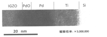
- FIG. 4 is a cross-sectional TEM image of a laminated electrode produced in Example 2.
- FIG. 6 is a cross-sectional view schematically showing elements produced in Examples 16 to 28.
- One embodiment of the laminate of the present invention includes a substrate, one or more layers selected from a contact resistance reduction layer and a reduction suppression layer, a Schottky electrode layer, and a metal oxide semiconductor layer in this order.
- the Schottky barrier diode can be formed regardless of the substrate and the base material.
- One or more layers selected from the contact resistance reduction layer and the reduction suppression layer are preferably in contact with the Schottky electrode layer, and the Schottky electrode layer and the metal oxide semiconductor layer are preferably in contact.
- Another embodiment of the laminate of the present invention has at least a Schottky electrode layer and a metal oxide semiconductor layer in this order on a conductive substrate, and reduces contact resistance between the conductive substrate and the Schottky electrode layer. It has one or more layers selected from a layer and a reduction suppression layer.
- the one embodiment of the laminate of the present invention and the other embodiment of the laminate of the invention are collectively referred to as the laminate of the present invention.
- the contact resistance reducing layer and the reduction suppressing layer may include both or only one of them.
- the laminated body of this invention may laminate
- the laminate according to the present invention has the above-described configuration, so that the on-resistance in the forward direction can be reduced when used in a semiconductor element. Further, the reverse leakage current can be reduced, the power loss can be reduced, and the current can be extracted.
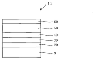
- Examples of the layer structure of the laminate of the present invention include the following structures. (1) substrate // contact resistance reduction layer / Schottky electrode layer / metal oxide semiconductor layer (2) substrate // reduction suppression layer / Schottky electrode layer / metal oxide semiconductor layer (3) substrate // contact resistance reduction Layer / reduction suppression layer / Schottky electrode layer / metal oxide semiconductor layer (“/” indicates that each layer is laminated adjacently) ("//" indicates that the layers are stacked without being adjacent to each other.)
- the following structure can be mentioned as a layer structure which laminated
- substrate // contact resistance reduction layer / Schottky electrode layer / metal oxide semiconductor layer / ohmic electrode layer (5) substrate // reduction suppression layer / Schottky electrode layer / metal oxide semiconductor layer / ohmic electrode layer ( 6)
- Substrate // Contact resistance reduction layer / Reduction suppression layer / Schottky electrode layer / Metal oxide semiconductor layer / Ohmic electrode layer
- the laminated structure (6) above is shown in FIG.
- the contact resistance reducing layer 20, the reduction suppressing layer 30, the Schottky electrode layer 40, the metal oxide semiconductor layer 50, and the ohmic electrode layer 60 are stacked in this order on the substrate 9.
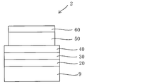
- the outer edge (end part) of the metal oxide semiconductor layer 50 may be the same as the outer edge (end part) of the Schottky electrode layer 40 or may be located inside the outer edge of the Schottky electrode layer 40. Good. The latter case is shown as a laminate 2 in FIG.
- symbol shall mean the same structure.
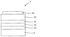
- the outer edge (end portion) of the ohmic electrode layer 60 may be the same as the outer edge (end portion) of the metal oxide semiconductor layer 50 or may be positioned inside the outer edge of the metal oxide semiconductor layer 50. May be. The latter case is shown as a laminate 3 in FIG. Each configuration will be described later.
- conductive substrate / contact resistance reduction layer / Schottky electrode layer / metal oxide semiconductor layer (12) conductive substrate / reduction suppression layer / Schottky electrode layer / metal oxide semiconductor layer (13) conductive substrate / Contact resistance reduction layer / reduction suppression layer / Schottky electrode layer / metal oxide semiconductor layer (“/” indicates that each layer is laminated adjacently)
- the following structure can also be mentioned as a layer structure which laminated
- Conductive substrate / contact resistance reduction layer / Schottky electrode layer / metal oxide semiconductor layer / ohmic electrode layer (15) Conductive substrate / reduction suppression layer / Schottky electrode layer / metal oxide semiconductor layer / ohmic electrode Layer (16) conductive substrate / contact resistance reduction layer / reduction suppression layer / Schottky electrode layer / metal oxide semiconductor layer / ohmic electrode layer
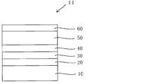
- FIG. 4 shows the layered structure (16) above.
- the contact resistance reducing layer 20, the reduction suppressing layer 30, the Schottky electrode layer 40, the metal oxide semiconductor layer 50, and the ohmic electrode layer 60 are stacked in this order on the conductive substrate 10.
- the outer edge (end part) of the metal oxide semiconductor layer 50 may be the same as the outer edge (end part) of the Schottky electrode layer 40 or may be located inside the outer edge of the Schottky electrode layer 40. Good. The latter case is shown as a laminate 12 in FIG. In this case, the Schottky electrode layer 40 covers the lower surface of the metal oxide semiconductor layer 50, that is, the entire lower surface of the metal oxide semiconductor layer 50 is in contact with the Schottky electrode layer 40.
- the end of the semiconductor is not in direct contact with the Schottky electrode in order to achieve a high withstand voltage.
- the metal oxide semiconductor since the metal oxide semiconductor has little leakage current at the film end, the end of the metal oxide semiconductor layer can be the same as or inside the end of the Schottky metal layer. Become. By doing so, it is possible to prevent the electric field from concentrating on the end portion of the semiconductor layer when a reverse bias is applied, and to realize a high withstand voltage.
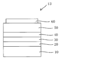
- the outer edge (end portion) of the ohmic electrode layer 60 may be the same as the outer edge (end portion) of the metal oxide semiconductor layer 50 or may be positioned inside the outer edge of the metal oxide semiconductor layer 50. May be. The latter case is shown as a laminate 13 in FIG. In this case, the metal oxide semiconductor layer 50 is configured to cover the lower surface of the ohmic electrode layer 60.
- FIGS. 2 and 3 can be applied to a stacked configuration other than the stacked configuration of Formula (6). Moreover, the structure shown in FIG. 2 and FIG. 3 can also be provided simultaneously. 5 and FIG. 6 can also be applied to a stacked configuration other than the stacked configuration of Expression (16). Moreover, the structure shown in FIG. 5 and FIG. 6 can also be provided simultaneously.
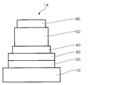
- FIG. 7 shows another embodiment of the laminated structure (16).
- the laminated body 14 in FIG. 7 has a laminated structure in which the structures shown in FIGS. 5 and 6 are provided at the same time, and the outer edge (end part) of the Schottky electrode layer 40 is the outer edge (end part) of the reduction suppressing layer 30.
- the outer edge (end part) of the contact resistance reducing layer 20 is located inside the outer edge (end part) of the conductive substrate 10.
- the substrate is not particularly limited and a known material can be used, and examples thereof include a conductive substrate, a semiconductor substrate, and an insulating substrate.
- the conductive substrate examples include a silicon substrate and a metal substrate.
- a low-resistance silicon substrate having a high impurity doping concentration is preferable, and an n-type low-resistance silicon substrate is more preferable.
- Conventionally known B, P, Pb, As, etc. can be used as the dopant.
- the silicon substrate preferably has a low resistance.
- the volume resistivity ⁇ of the silicon substrate is preferably 100 m ⁇ cm or less, more preferably 10 m ⁇ cm or less, and further preferably 5 m ⁇ cm or less.
- the metal of the metal substrate examples include Cu, Al, Au, Cr, Fe, Ni, and W. These alloys can also be used. Preferably, Cu, Al, or an alloy thereof is low resistance, low cost, and excellent thermal conductivity. When a metal substrate is used as the conductive substrate, this metal substrate can also serve as a contact resistance reducing layer.
- the laminate of the present invention can provide a Schottky barrier diode that exhibits good diode characteristics even when an inexpensive silicon substrate or metal substrate is used as a conductive substrate.
- the thickness of the conductive substrate is usually 200 ⁇ m to 2 mm.
- the material of the semiconductor substrate is not particularly limited as long as the surface smoothness is maintained.
- a semiconductor substrate a Si substrate, a GaN substrate, a SiC substrate, a GaP substrate, a GaAs substrate, a ZnO substrate, a Ga 2 O 3 substrate, a GaSb substrate, an InP substrate, and an InAs whose carrier concentration is adjusted to 1 ⁇ 10 18 cm ⁇ 3 or less.
- Examples include a substrate, an InSb substrate, a ZnS substrate, a ZnTe substrate, and a diamond substrate.
- the semiconductor substrate may be single crystal or polycrystalline. Further, an amorphous substrate or a substrate partially containing amorphous may be used.
- a substrate in which a semiconductor film is formed using a technique such as CVD (chemical vapor deposition) on a conductor substrate, a semiconductor substrate, or an insulating substrate may be used.
- the thickness of the semiconductor substrate is usually 200 ⁇ m to 2 mm.
- the thickness is preferably 200 ⁇ m to 1 mm, more preferably 200 ⁇ m to 700 ⁇ m.
- the insulating substrate is not particularly limited as long as it is an insulating substrate, and a substrate generally used can be arbitrarily selected as long as the effects of the present invention are not lost.
- a substrate generally used can be arbitrarily selected as long as the effects of the present invention are not lost.
- the insulating substrate for example, quartz glass, barium borosilicate glass, aluminoborosilicate glass, aluminosilicate glass, etc., alkali-free glass substrate produced by the fusion method or float method, ceramic substrate, and processing temperature of this production process And a plastic substrate having heat resistance that can withstand heat.
- a dielectric substrate may also be used as the insulating substrate.
- the dielectric substrate include a lithium niobate substrate, a lithium tantalate substrate, a zinc oxide substrate, a quartz substrate, and a sapphire substrate.
- an insulating substrate or a dielectric substrate in which an insulating film or a dielectric film is provided on the surface of a metal substrate such as a stainless alloy may be used.
- an insulating film may be formed over the substrate as a base film.
- a single layer or a stacked layer such as a silicon oxide film, a silicon nitride film, a silicon oxynitride film, or a silicon nitride oxide film can be formed by a CVD method, a sputtering method, or the like.
- the thickness of the insulating substrate is not particularly limited, but is 2 ⁇ m to 2 mm, for example.
- the thickness is preferably 2 ⁇ m to 1 mm, more preferably 2 ⁇ m to 700 ⁇ m.
- a base material having an arbitrary structure, layer structure, circuit, wiring, electrode, or the like made of a plurality of materials may be used on the above-described conductive substrate, semiconductor substrate, or insulating substrate.
- Examples of materials having an arbitrary structure include composite materials of various metals and insulators such as a metal that forms a back end of line on a large scale integrated circuit (LSI), an interlayer insulating film, and the like.
- LSI large scale integrated circuit
- interlayer insulating film and the like.
- substrate is not specifically limited, Preferably it is 150 nm or less, More preferably, it is 50 nm or less, More preferably, it is 10 nm or less.
- the smoothness of the Schottky electrode layer is maintained when the contact resistance reduction layer, the reduction suppression layer, and the Schottky electrode layer are stacked, and the device is evaluated as an element. The leakage current in the reverse direction is kept low.
- the surface roughness of the substrate can be determined, for example, by the method described in the examples.
- the layer structure is not particularly limited, and is an electrode layer, an insulating layer, a semiconductor layer, a dielectric layer, a protective film layer, a stress buffer layer, a light shielding layer, an electron / hole injection layer, an electron / hole transport layer, a light emitting layer.
- Known layers such as an electron / hole blocking layer, a crystal growth layer, an adhesion improving layer, a memory layer, a liquid crystal layer, a capacitor layer, and a power storage layer can be used.
- an insulating layer generally Al, Si, Sc, Ti, V, Cr, Ni, Cu, Zn, Ga, Ge, Y, Zr, Nb, Mo, Tc, Ru, Rh, Pd, Ag, Cd, In, Examples thereof include an oxide insulating film and a nitride film containing one or more metals selected from the group consisting of Sn, Sb, Te, Hf, Ta, W, Re, Os, Ir, Pt, and Au.
- oxide semiconductor layers, organic semiconductor layers such as pentacene, and the like are widely used regardless of the crystalline state of single crystal, polycrystal, or amorphous.
- a lithium niobate layer As the dielectric layer, a lithium niobate layer, a lithium tantalate layer, a zinc oxide layer, a quartz substrate layer, a sapphire layer, a BaTiO 3 layer, a Pb (Zr, Ti) O 3 (PZT) layer, (Pb, La) ( Zr, Ti) O 3 (PLZT) layer, Pb (Zr, Ti, Nb) O 3 (PZTN) layer, Pb (Ni, Nb) O 3 —PbTiO 3 (PNN-PT) layer, Pb (Ni, Nb) O 3 —PbZnO 3 (PNN—PZ) layer, Pb (Mg, Nb) O 3 —PbTiO 3 (PMN—PT) layer, SrBi 2 Ta 2 O 9 (SBT) layer, (K, Na) TaO 3 layer, (K, Na) NbO 3 layer, BiFeO 3 layer, Bi (Nd, La
- the protective film layer As a film of the protective film layer, a film having excellent insulating properties regardless of inorganic materials and organic materials and low permeability of water or the like can be used.
- Examples of the stress buffer layer include an AlGaN layer.
- Examples of the light shielding layer include a black matrix layer containing a metal, a metal-organic material, and a color filter layer.
- Examples of the electron / hole injection layer include an oxide semiconductor layer and an organic semiconductor layer.
- Examples of the electron / hole transport layer include an oxide semiconductor layer and an organic semiconductor layer.
- Examples of the light emitting layer include an inorganic semiconductor layer and an organic semiconductor layer.
- Examples of the electron / hole blocking layer include an oxide semiconductor layer.
- Examples of the base material include a power generation device, a light emitting device, a sensor, a power conversion device, an arithmetic device, a protection device, an optoelectronic device, a display, a memory, a semiconductor device having a back end of line, and a power storage device.
- the layer having a layer structure may be a single layer or two or more layers.
- the contact resistance reducing layer plays a role of preventing the interaction between the base substrate and the Schottky electrode metal. In addition, it improves the adhesion of the Schottky electrode to the underlying substrate and improves the surface smoothness of the Schottky electrode. That is, it is a layer for reducing the contact resistance when the substrate and the Schottky electrode are directly laminated.
- the substrate and the Schottky electrode are directly laminated, for example, when an n-type low-resistance silicon substrate is used as the substrate and these are directly laminated using palladium oxide for the Schottky electrode, the palladium oxide and Si are in the opposite directions. A -n junction is formed and becomes a large resistance component in the forward direction. Further, the interface between Si and palladium oxide is not smooth, and as a result, the smoothness of the surface of the Schottky electrode is lost, and there is a possibility that the withstand voltage is lowered.
- one or more metals selected from Ti, Mo, Ag, In, Al, W, Co, and Ni, alloys thereof, or silicides thereof can be used.
- Ti, Mo, Ag, In, or Al that forms a low-resistance silicide and more preferably Ti or Mo that forms a good Schottky contact when combined with a low-resistance and Schottky metal.
- Mo has a high thermal conductivity. Since Mo is excellent in heat dissipation and has high thermal conductivity, element degradation is less likely to occur due to Joule heat due to current when the diode is driven.
- the thickness of the contact resistance reducing layer is usually 1 nm to 1 ⁇ m, preferably 2 nm to 500 nm, more preferably 5 nm to 500 nm. If it is this range, it has sufficient adhesiveness and there is little increase in resistance. More preferably, it is 10 nm to 500 nm.
- the in-plane coverage of the contact resistance reducing layer is high, and it is easy to obtain characteristics with small in-plane resistance variation in the forward direction when the diode is driven. Furthermore, when used as an element for taking out a current in the lateral direction, the wiring resistance is lowered and a high current value is easily obtained.
- the contact resistance reduction layer can be confirmed by cross-sectional TEM observation or secondary ion mass spectrometry. The same applies to the ohmic electrode, the metal oxide semiconductor layer, the reduction suppressing layer, the Schottky electrode layer, and the substrate.
- the reduction suppression layer is a layer that prevents reduction of the Schottky electrode layer. If the reduction suppressing layer is provided, the reduction of the Schottky electrode layer is suppressed, and the Schottky interface is formed without any problem.
- metal used for the reduction suppression layer one or more kinds selected from Pd, Mo, Pt, Ir, Ru, Au, Ni, W, Cr, Re, Te, Tc, Mn, Os, Fe, Rh, and Co. Element and these alloys are mentioned.
- the reduction suppressing layer that is, the metal oxide metal constituting the Schottky electrode layer.
- the combination of the reduction suppressing layer and the Schottky electrode layer include Pd / palladium oxide, Pt / platinum oxide, Ir / iridium oxide, Ru / ruthenium oxide, and the like.
- the thickness of the reduction suppressing layer is usually 1 nm to 1 ⁇ m, preferably 2 nm to 500 nm, more preferably 5 nm to 100 nm, and particularly preferably 10 nm to 50 nm. Within this range, since the reduction suppressing effect is excellent, the on-resistance during forward bias can be reduced. In addition, the flatness of the Schottky interface can be improved.
- the work function of the metal contained in the Schottky electrode layer is preferably 3.7 eV or more, more preferably 4.4 eV or more, and further preferably 4.7 eV or more.
- the upper limit of the work function is not particularly specified, but is usually 6.5 eV.
- Pd oxide, Pt oxide, Ir oxide or Ru oxide is preferable.
- a high Schottky barrier can be formed by a combination with a metal oxide semiconductor.
- the carrier concentration of the Schottky electrode layer is preferably 1 ⁇ 10 18 cm ⁇ 3 or more.
- the carrier concentration can be obtained, for example, by hole measurement.
- the thickness of the Schottky electrode layer is usually 1 nm to 1 ⁇ m, preferably 2 nm to 100 nm, more preferably 5 nm to 50 nm. Within this range, the on-resistance during forward bias is excellent. In addition, the flatness of the Schottky interface can be improved and the voltage resistance is excellent.
- the production method for obtaining the metal oxide of the Schottky electrode is not particularly limited, and examples thereof include a method of performing reactive sputtering of a metal target in an oxygen-containing atmosphere.
- the composition of the metal oxide semiconductor layer is not particularly limited as long as it is a metal oxide semiconductor.
- An oxide containing one or more elements selected from In, Ga, Zn, and Sn is preferable. Examples thereof include an oxide semiconductor (IGZO) of In, Ga, and Zn.
- IGZO oxide semiconductor
- Hydrogen concentration of the metal oxide semiconductor layer is preferably from 10 17 to 10 22 / cm 3, more preferable to be 10 19 to 10 22 / cm 3, more preferably 10 20 to 10 21 / cm 3.
- Oxide semiconductors easily form oxygen vacancies, and leakage current may flow through the vacancies. However, oxygen vacancies are terminated with hydroxyl groups by increasing the hydrogen atom concentration in the film to 10 20 atoms / cm 3 or more. Leakage current can be reduced.
- the hydrogen atom concentration is measured by secondary ion mass spectrometry.
- the method for adjusting the hydrogen atom concentration is not particularly limited, but can be adjusted by optimizing the atmosphere during film formation, annealing after film formation, and the atmosphere during film formation of the ohmic electrode.
- the free carrier concentration of the metal oxide semiconductor layer is usually 1 ⁇ 10 13 cm ⁇ 3 or more and less than 1 ⁇ 10 18 cm ⁇ 3 .
- the free carrier concentration can be obtained, for example, by hole measurement.
- the band gap of the metal oxide semiconductor layer is preferably 2.0 eV to 6.0 eV, more preferably 2.5 eV to 5.5 eV, and further preferably 3.0 eV to 5.0 eV.
- the band gap is measured by the method described in the examples.
- the thickness of the metal oxide semiconductor layer is usually 10 nm to 10 ⁇ m, preferably 50 nm to 7 ⁇ m, more preferably 100 nm to 5 ⁇ m.
- the film thickness can be selected so as to obtain a desired withstand voltage. If it is too thick, the resistance during forward bias may increase.
- the laminate of the present invention can provide a Schottky barrier diode that exhibits good diode characteristics even when a metal oxide semiconductor layer is formed by a method having excellent productivity such as sputtering.
- the material of the ohmic electrode layer is not particularly limited as long as a good ohmic connection with the metal oxide semiconductor layer can be achieved, but one or more elements selected from the group consisting of Mo, Ti, Au, Ag, and Al and alloys thereof Is mentioned.
- the ohmic electrode layer can be composed of a plurality of layers.
- a Mo electrode layer can be used on the side in contact with the metal oxide semiconductor layer, and a metal layer of Au or Al can be stacked. In this way, power loss can be reduced and current can be extracted.
- the thickness of the ohmic electrode layer is not particularly limited, but is usually 100 nm to 5 ⁇ m.
- the film forming method of each layer is not particularly limited, but the CVD method such as thermal CVD method, CAT-CVD method, photo CVD method, mist CVD method, MO-CVD method, plasma CVD method, atomic level control such as MBE, ALD, etc.
- CVD method such as thermal CVD method, CAT-CVD method, photo CVD method, mist CVD method, MO-CVD method, plasma CVD method, atomic level control such as MBE, ALD, etc.
- Conventionally known ceramic processes such as PVD methods such as film forming method, ion plating, ion beam sputtering, magnetron sputtering, doctor blade method, injection method, extrusion method, hot press method, sol-gel method, aerosol deposition method are used.
- a wet method such as a method, a coating method, a spin coating method, a printing method, a spray method, an electrodeposition method, a plating method, or a micellar electrolysis method can be used.
- the laminated body of the present invention includes a power semiconductor element, a (rectifier) diode element, a Schottky barrier diode element, an electrostatic discharge (ESD) protection diode, a transient voltage protection (TVS) protection diode, a light emitting diode, and a metal semiconductor field effect transistor (MESFET). ), Junction field effect transistor (JFET), metal oxide semiconductor field effect transistor (MOSFET), Schottky source / drain MOSFET, avalanche multiplication type photoelectric conversion element, solid-state imaging device, solar cell element, photosensor element, display It can be used for semiconductor elements such as elements and resistance change memories.
- the semiconductor element can be used for a Schottky barrier diode or a junction transistor.
- An electronic circuit using this element, a Schottky barrier diode, or a junction transistor can be used in an electric device, an electronic device, a vehicle, a power engine, and the like.
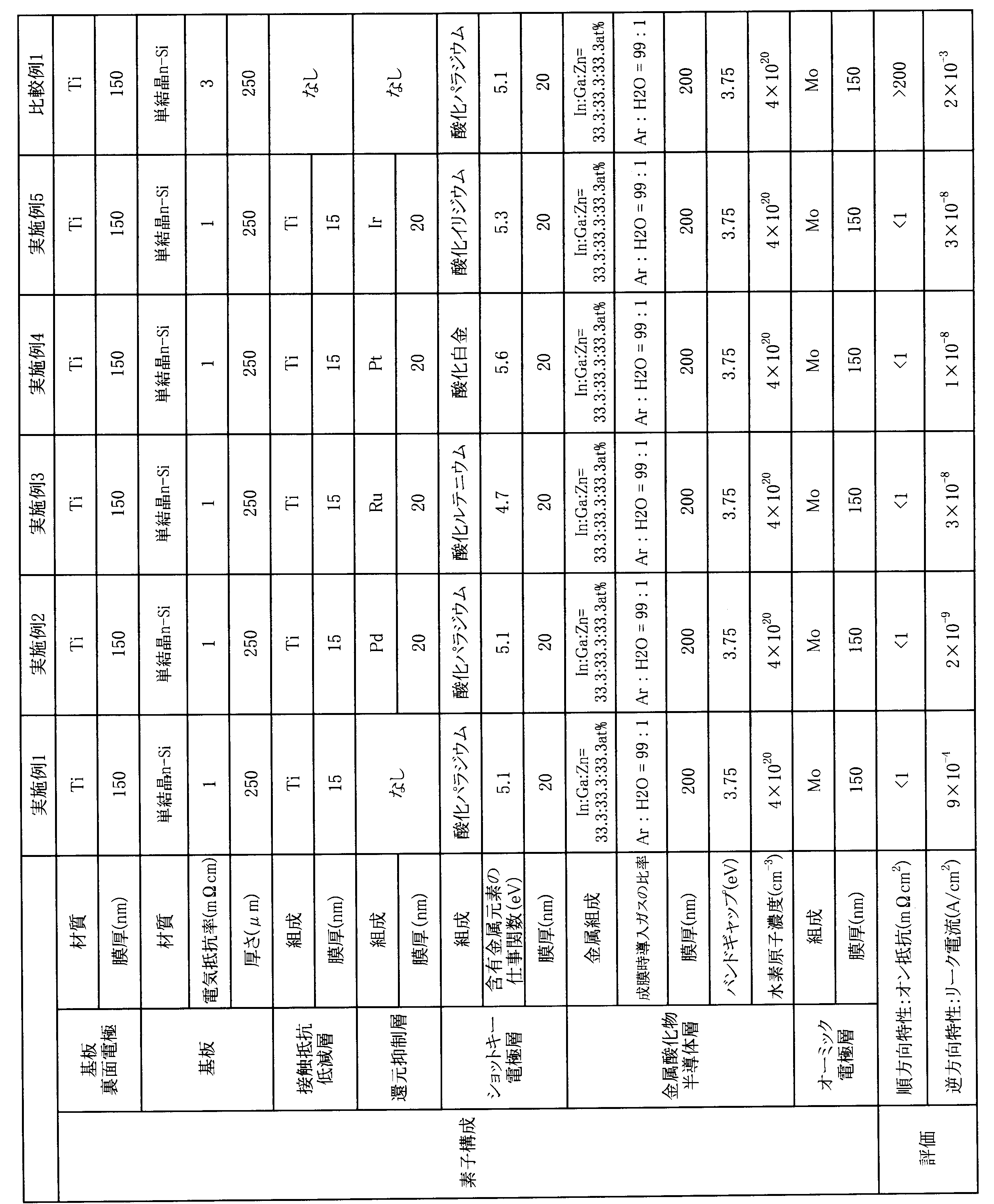
- Example 1 [Production of Schottky barrier diode] A Schottky barrier diode element was fabricated as follows. An n-type Si substrate (diameter 4 inches) having a resistivity of 1 m ⁇ ⁇ cm was mounted on a sputtering apparatus (manufactured by Anelva: E-200S), and Ti was deposited to a thickness of 15 nm as a contact resistance reducing layer. The film forming conditions were a DC 50 W, Ar atmosphere. Next, 10 nm of palladium oxide was deposited as a Schottky electrode layer (carrier concentration: 1 ⁇ 10 20 cm ⁇ 3 ). Film forming conditions, DC50W, and a mixed gas atmosphere of Ar and O 2.
- this substrate was set in a sputtering apparatus (ULVAC: CS-200) together with Area Max, and 200 nm of IGZO having the composition shown in Table 1 was formed as a metal oxide semiconductor layer (free carrier concentration: 5 ⁇ 10 16 cm ⁇ 3 ).
- the film forming conditions were DC 300 W and a gas flow rate ratio shown in Table 1.
- the substrate was taken out and annealed in an electric furnace at 300 ° C. for 1 hour in air.
- This substrate was set again in a sputtering apparatus together with Area Max, and then Mo was deposited to a thickness of 150 nm as an ohmic electrode layer.
- the film forming conditions were DC 100 W, Ar atmosphere.
- the free carrier concentration of the metal oxide semiconductor layer and the carrier concentration of the Schottky electrode layer were measured as follows. It performed through the metal oxide semiconductor layer film-forming process (or Schottky electrode layer film-forming process) with respect to the glass substrate. Then, each substrate was cut into 1 cm square, and In electrodes were provided at the four corners to obtain Hall effect measurement elements.
- the free carrier concentration (carrier concentration) is measured at room temperature using a Hall effect measuring device (manufactured by ACCENT: HL-5500PC), and the resulting free carrier amount (carrier amount) is measured on the metal semiconductor layer.
- the free carrier concentration (carrier concentration) was normalized by the volume (or the Schottky electrode volume).
- the band gap of the metal oxide semiconductor layer was evaluated as follows. The process up to the step of forming the metal oxide semiconductor layer in the above Schottky barrier diode manufacturing process was performed on the substrate, and the obtained laminate was cut into 1 cm square. Using a spectroscopic ellipsometry measuring device (manufactured by JA Woollam Japan Co., Ltd .: M-2000D) at room temperature, the incident angle of polarized light is changed to 50 °, 60 °, 70 ° from the direction perpendicular to the substrate, The measurement was performed at a measurement wavelength of 192.3 nm to 1689 nm and a measurement width of 3.4 nm.
- the absorption coefficient ⁇ was calculated.
- the spectrum of the absorption coefficient alpha of the metal oxide semiconductor layer, by plotting the alpha 2 relative to the energy range 2 eV ⁇ 5 eV of light was calculated intersection of the energy axis which is extended linearly as a band gap. The results are shown in Table 1.
- the hydrogen atom concentration of the metal oxide semiconductor layer was evaluated as follows. The measurement was carried out by a quadrupole secondary ion mass spectrometer (manufactured by ULVAC-PHI, Inc .: D-SIMS) under measurement conditions of a Cs ion source of 1 kV, a primary ion current of 100 nA, and a chamber vacuum degree of 5 ⁇ 10 ⁇ 10 torr.
- the hydrogen atom concentration of the metal oxide semiconductor layer is determined based on the hydrogen secondary ion intensity obtained by the quadrupole secondary ion mass spectrometer integrated with the thickness of the metal semiconductor thin film.
- the strength was normalized by using an In—Ga—Zn—O thin film with a known concentration and film thickness, and the hydrogen concentration was quantified. The obtained value was defined as the hydrogen atom concentration.
- Table 1 The results are shown in Table 1.
- Example 2 A device was fabricated in the same manner as in Example 1 except that 20 nm of Pd was deposited as a reduction suppressing layer following the formation of the contact resistance reducing layer.
- the film forming conditions were a DC 50 W, Ar atmosphere.
- a cross-sectional TEM image obtained by an electron microscope (manufactured by JEOL: JEM-2800) of the laminated electrode is shown in FIG.
- the obtained element Si / Ti / Pd / palladium oxide / IGZO / Mo
- the obtained element was evaluated in the same manner as in Example 1. The results are shown in Table 1.
- the obtained element has a structure shown in FIG.
- Example 3 Following the formation of the contact resistance reducing layer, a device was fabricated in the same manner as in Example 1 except that Ru was deposited to a thickness of 20 nm as a reduction suppressing layer and then ruthenium oxide was deposited to a thickness of 10 nm as a Schottky electrode.
- the Ru film formation conditions were DC 50 W, Ar atmosphere, and the ruthenium oxide film formation conditions were DC 50 W, a mixed gas atmosphere of Ar and O 2 (carrier concentration: 1 ⁇ 10 20 cm ⁇ 3 ).
- the obtained element Si / Ti / Ru / ruthenium oxide / IGZO / Mo
- the obtained element was evaluated in the same manner as in Example 1. The results are shown in Table 1.
- the obtained element has a structure shown in FIG.
- Example 4 Following the formation of the contact resistance reducing layer, a device was fabricated in the same manner as in Example 1 except that 20 nm of Pt was formed as a reduction suppressing layer and then 10 nm of platinum oxide was formed as a Schottky electrode.
- the Pt film formation conditions were DC 50 W and Ar atmosphere, and the platinum oxide film formation conditions were DC 50 W and a mixed gas atmosphere of Ar and O 2 (carrier concentration: 1 ⁇ 10 20 cm ⁇ 3 ).
- the obtained element Si / Ti / Pt / platinum oxide / IGZO / Mo
- the obtained element was evaluated in the same manner as in Example 1. The results are shown in Table 1.
- the obtained element has a structure shown in FIG.
- Example 5 Following the formation of the contact resistance reducing layer, an element was fabricated in the same manner as in Example 1 except that Ir was deposited to a thickness of 20 nm as a reduction suppression layer, and then iridium oxide was deposited to a thickness of 10 nm as a Schottky electrode.
- the Ir film formation conditions were DC 50 W and Ar atmosphere, and the iridium oxide film formation conditions were DC 50 W and a mixed gas atmosphere of Ar and O 2 (carrier concentration: 1 ⁇ 10 20 cm ⁇ 3 ).
- the obtained element Si / Ti / Ir / iridium oxide / IGZO / Mo
- the obtained element was evaluated in the same manner as in Example 1. The results are shown in Table 1.
- the obtained element has a structure shown in FIG.
- the devices obtained in Examples 2 to 5 exhibited good diode characteristics with an on-resistance Ron of less than 1 m ⁇ cm 2 and a leakage current Ir of 3 ⁇ 10 ⁇ 8 A / cm
- Comparative Example 1 A device was fabricated in the same manner as in Example 1 except that the contact resistance reducing layer was not formed.
- the obtained element Si / palladium oxide / IGZO / Mo
- the results are shown in Table 1.
- the device obtained in Comparative Example 1 had a high on-resistance Ron of 200 m ⁇ cm 2 or more, and the leakage current Ir was 2 ⁇ 10 ⁇ 3 A / cm 2 .
- Examples 6-9 A device was fabricated in the same manner as in Example 2 except that the reduction suppressing layer and the Schottky electrode layer were changed to the combinations shown in Table 2 with respect to Example 2. The obtained device was evaluated in the same manner as in Example 1. The results are shown in Table 2. The devices obtained in Examples 6 to 9 exhibited good diode characteristics with an on-resistance Ron of less than 10 m ⁇ cm 2 and a leakage current Ir of 5 ⁇ 10 ⁇ 8 A / cm 2 or less.
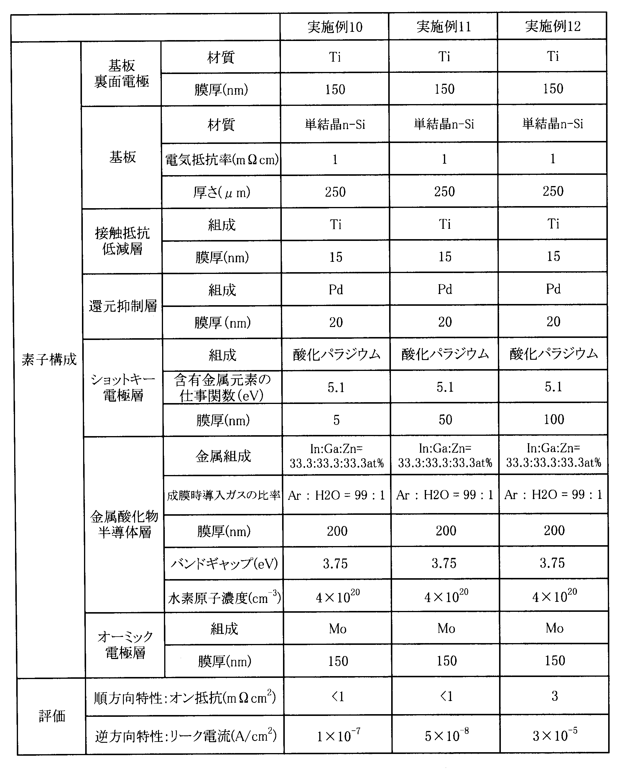
- Examples 10-12 A device was fabricated in the same manner as in Example 2 except that the thickness of the Schottky electrode layer was changed as described in Table 3 with respect to Example 2. The obtained device was evaluated in the same manner as in Example 1. The results are shown in Table 3.
- the devices obtained in Examples 10 and 11 had good diode characteristics with an on-resistance Ron of less than 1 m ⁇ cm 2 and a leakage current Ir of 1 ⁇ 10 ⁇ 7 A / cm 2 or less.
- the device obtained in Example 12 had an on-resistance Ron of less than 10 m ⁇ cm 2 and a leakage current Ir of 3 ⁇ 10 ⁇ 5 A / cm 2 or less.
- Examples 13-15 A device was fabricated in the same manner as in Example 2 except that the Schottky electrode layer and the reduction suppression layer were changed as described in Table 4 with respect to Example 2. The obtained device was evaluated in the same manner as in Example 1. The results are shown in Table 4.
- the device obtained in Example 13 had good diode characteristics with an on-resistance Ron of less than 1 m ⁇ cm 2 and a leakage current Ir of 5 ⁇ 10 ⁇ 7 A / cm 2 or less.
- the devices obtained in Examples 14 and 15 had a low on-resistance Ron of less than 1 m ⁇ cm 2 , and the leakage currents Ir were 2 ⁇ 10 ⁇ 3 A / cm 2 and 7 ⁇ 10 ⁇ 1 A / cm 2 , respectively. there were.
- Examples 16-19 An element was manufactured on a substrate shown in Table 5 using a photomask.
- the film forming conditions of Example 2 and each layer are the same.
- FIG. 9 shows the structure of the obtained element (laminated body) 15.
- Ti was sputtered on the one surface of the substrate 8 as the contact resistance reducing layer 20, and Pd was sputtered as the reduction suppressing layer 30 at 15 nm and 20 nm, respectively.
- the Ti / Pd laminated film was patterned using a photomask.
- AZ1500 manufactured by AZ Electronic Materials
- TMAH tetramethylammonium hydroxide
- AURUM-302 manufactured by Kanto Chemical
- AZ5214 manufactured by AZ Electronic Materials
- AZ5214 was exposed through a photomask, exposed on the entire surface after the reverse baking step, and developed with tetramethylammonium hydroxide (TMAH).
- TMAH tetramethylammonium hydroxide
- the interlayer insulating film 70 was patterned using a thermosetting non-photosensitive polyimide and a photomask. Specifically, first, a thermosetting non-photosensitive polyimide solution was applied on the entire surface of the substrate with a spin coater, and then patterned using AZ5214 and a photomask. AZ5214 was exposed through a photomask, exposed on the entire surface after the reverse baking step, and developed with tetramethylammonium hydroxide (TMAH). Subsequently, the thermosetting non-photosensitive polyimide was etched with TMAH and patterned. After patterning, the thermosetting non-photosensitive polyimide was heated and cured in the atmosphere at 200 ° C. for 1 hour.
- TMAH tetramethylammonium hydroxide
- the ohmic electrode layer 60 was patterned by a lift-off process using an image reversal resist AZ5214 and a photomask.
- AZ5214 was exposed through a photomask, exposed on the entire surface after the reverse baking step, and developed with tetramethylammonium hydroxide (TMAH).
- TMAH tetramethylammonium hydroxide
- Mo 150 nm was deposited as an ohmic electrode layer, and then an Au layer 80 was deposited to 500 nm. Thereafter, the ohmic electrode layer 60 was patterned by lifting off in acetone.
- the element was measured by grounding the probe on the ohmic electrode side and connecting it to the ground, grounding the probe in a region where the ohmic electrode and Au were directly laminated on the reduction suppression layer, and changing the voltage. Other evaluations were performed in the same manner as in Example 1. The results are shown in Table 5.
- the carrier concentration of the Schottky electrode layer was 1 ⁇ 10 20 cm ⁇ 3 .
- the devices obtained in Examples 16 to 18 had good diode characteristics with an on-resistance Ron of less than 1 m ⁇ cm 2 and a leakage current Ir of 5 ⁇ 10 ⁇ 8 A / cm 2 or less.
- the device obtained in Example 19 had a leakage current Ir of 1 ⁇ 10 ⁇ 1 A / cm, which was higher than those in Examples 16 to 18.
- the surface roughness of the substrate was measured by observing the fabricated device with a cross-sectional TEM (transmission electron microscope) image and EDX (energy dispersive X-ray spectroscopy). The specific procedure is shown below.
- the area where the constituent elements of each substrate shown in Table 5 were detected by EDX was defined as the substrate, and the interface was defined from the difference in contrast between the substrate and the ohmic electrode layer in the cross-sectional TEM image.
- the arithmetic average roughness Ra was calculated from the equation (1) with respect to the unevenness of the substrate interface to obtain surface roughness. The results are shown in Table 5.
- the crystallinity of the substrate was evaluated by an electron diffraction image obtained by an electron microscope (manufactured by JEOL: JEM-2800). In the electron beam irradiation area, a diffraction image was obtained from a region having a diameter of 10 nm or more with respect to the cross section of the substrate. Those in which the spot shape was observed in the diffraction image were judged as single crystals, and those in the ring shape were judged as polycrystalline. The results are shown in Table 5.
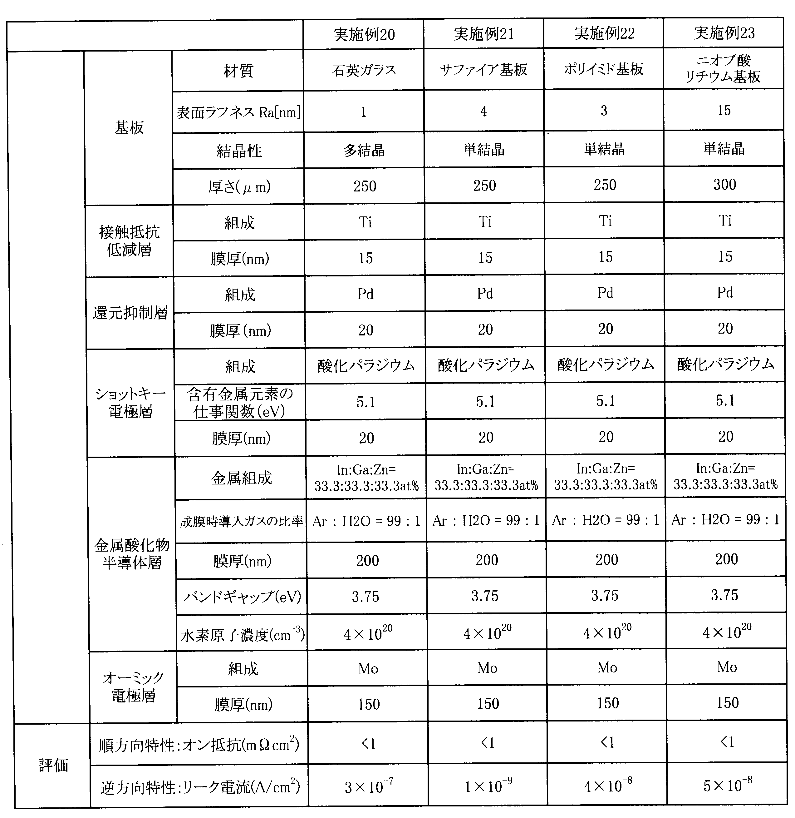
- Examples 20-23 A device was fabricated in the same manner as in Example 16 except that the insulating substrate shown in Table 6 was used. The obtained device was evaluated in the same manner as in Example 16. The results are shown in Table 6. The carrier concentration of the Schottky electrode layer was 1 ⁇ 10 20 cm ⁇ 3 . The devices obtained in Examples 20 to 23 exhibited good diode characteristics with an on-resistance Ron of less than 1 m ⁇ cm 2 and a leakage current Ir of 3 ⁇ 10 ⁇ 7 A / cm 2 or less.
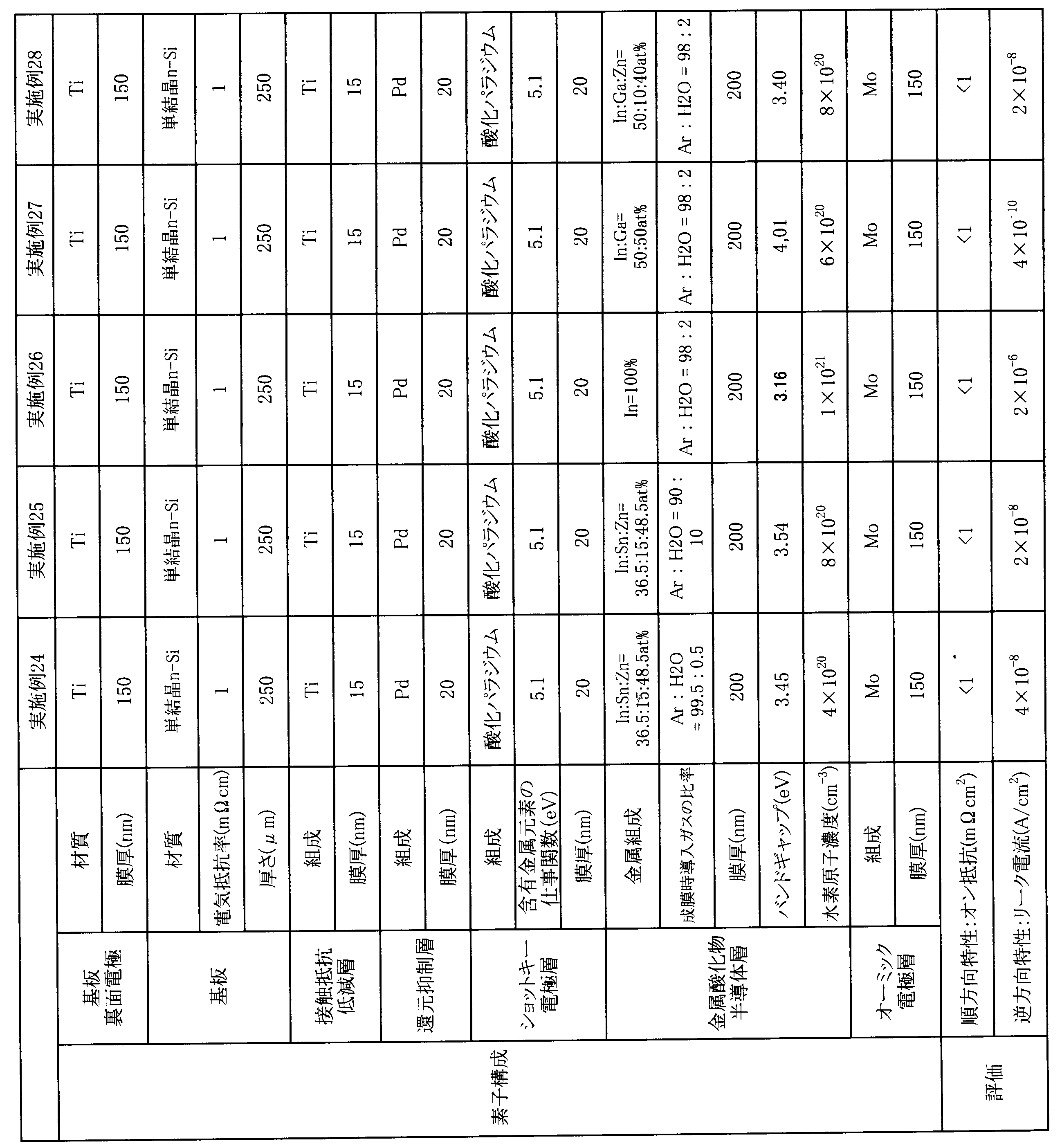
- Examples 24-28 A device was fabricated in the same manner as in Example 2 except that the metal oxide semiconductor layer was formed with the metal composition shown in Table 7 and the ratio of the introduced gas during film formation. The obtained device was evaluated in the same manner as in Example 1. The results are shown in Table 7. The obtained element has a structure shown in FIG. The devices obtained in Examples 24 to 28 exhibited good diode characteristics with an on-resistance Ron of less than 1 m ⁇ cm 2 and a leakage current Ir of 2 ⁇ 10 ⁇ 6 A / cm 2 or less.
- Examples 29-33 A device was fabricated in the same manner as in Example 2 except that the metal oxide semiconductor layer was formed with the metal composition shown in Table 8 and the ratio of the introduced gas during film formation. The obtained device was evaluated in the same manner as in Example 1. The results are shown in Table 8. As a result of evaluating the hydrogen atom concentration of the devices obtained in Examples 29 to 31, they were 8 ⁇ 10 20 cm ⁇ 3 , 5 ⁇ 10 21 cm ⁇ 3 , and 5 ⁇ 10 20 cm, respectively. The devices obtained in Examples 29 to 31 exhibited good diode characteristics with an on-resistance Ron of less than 1 m ⁇ cm 2 and a leakage current Ir of 2 ⁇ 10 ⁇ 8 A / cm 2 or less.
- the hydrogen atom concentration of the devices obtained in Examples 32 and 33 were 4 ⁇ 10 15 cm ⁇ 3 and 8 ⁇ 10 16 cm ⁇ 3 , respectively.
- the devices obtained in Examples 32 and 33 had an on-resistance Ron of less than 1 m ⁇ cm 2 , but the leakage currents Ir were 9 ⁇ 10 ⁇ 1 A / cm 2 and 1 ⁇ 10 ⁇ 2 A / cm 2 , respectively. there were.
- Examples 34-35 A device was fabricated in the same manner as in Example 2 except that the contact resistance reducing layer or the ohmic electrode layer was changed to the material shown in Table 9. The obtained device was evaluated in the same manner as in Example 1. The results are shown in Table 9. The devices obtained in Examples 34 and 35 had an on-resistance Ron of less than 1 m ⁇ cm 2 , but the leakage currents Ir were 1 ⁇ 10 ⁇ 1 A / cm 2 and 3 ⁇ 10 ⁇ 8 A / cm 2 , respectively. There was good diode characteristics.
- the laminate of the present invention can be used for a semiconductor element such as a power semiconductor element, a diode element, and a Schottky barrier diode element, and an electronic circuit using the element is used for an electric device, an electronic device, an electric vehicle, and the like. Can do.
- a semiconductor element such as a power semiconductor element, a diode element, and a Schottky barrier diode element
Landscapes
- Electrodes Of Semiconductors (AREA)
- Chemical & Material Sciences (AREA)
- Crystallography & Structural Chemistry (AREA)
- Laminated Bodies (AREA)
Abstract
Description
β-Ga2O3はさらにバンドギャップが広く(4.8eV~4.9eV)、高い耐電圧性が期待されるが、やはり良質な基板の製造に課題があり、量産性とコストに課題がある。
1.基板と、接触抵抗低減層及び還元抑制層から選択される1以上の層と、ショットキー電極層と、金属酸化物半導体層とをこの順に有する積層体。
2.前記基板と、前記接触抵抗低減層と、前記還元抑制層とをこの順に有する1に記載の積層体。
3.前記還元抑制層が、Pd、Mo、Pt、Ir、Ru、Au、Ni、W、Cr、Re、Te、Tc、Mn、Os、Fe、Rh及びCoから選択される1種類以上の元素を含む1又は2に記載の積層体。
4.前記接触抵抗低減層が、Ti、Mo、Ag、In、Al、W、Co及びNiから選択される1以上の金属又はそのシリサイドを含む1~3のいずれかに記載の積層体。
5.前記ショットキー電極層が、仕事関数が4.4eV以上である1種類以上の元素の酸化物を含む1~4のいずれかに記載の積層体。
6.前記ショットキー電極層が、Pd、Mo、Pt、Ir、Ru、Ni、W、Cr、Re、Te、Tc、Mn、Os、Fe、Rh及びCoから選択される1以上の金属の酸化物を含む1~5のいずれかに記載の積層体。
7.前記基板が、導電性基板である1~6のいずれかに記載の積層体。
8.前記基板が、導電性のシリコン基板である1~6のいずれかに記載の積層体。
9.前記金属酸化物半導体層が、In、Sn、Ga、及びZnから選択される1種類以上の元素を含む1~8のいずれかに記載の積層体。
10.前記金属酸化物半導体層の水素原子濃度が1017~1022個/cm3である1~9のいずれかに記載の積層体。
11.前記金属酸化物半導体層上にオーミック電極層を有する1~10のいずれかに記載の積層体。
12.前記金属酸化物半導体層の外縁が、前記ショットキー電極層の外縁と同一であるか又は前記ショットキー電極層の外縁の内側に位置し、前記ショットキー電極層が前記金属酸化物半導体層の下面の全面に接する1~11のいずれかに記載の積層体。
13.前記オーミック電極層の外縁が、前記金属酸化物半導体層の外縁と同一であるか又は前記金属酸化物半導体層の外縁の内側に位置する11又は12に記載の積層体。
14.1~13のいずれかに記載の積層体を用いた半導体素子。
15.14に記載の半導体素子を用いたショットキーバリアダイオード。
16.14に記載の半導体素子を用いたジャンクショントランジスタ。
17.14に記載の半導体素子、15に記載のショットキーバリアダイオード、又は16に記載のジャンクショントランジスタを用いた電子回路。
18.17に記載の電子回路を用いた電気機器、電子機器、車両、又は動力機関。
本発明の積層体の一態様は、基板と、接触抵抗低減層及び還元抑制層から選択される1以上の層と、ショットキー電極層と、金属酸化物半導体層とをこの順に有する。
本発明の積層体の一態様では、ショットキーバリアダイオードを、基板、基材を選ばず形成できる。
基板と、接触抵抗低減層及び還元抑制層から選択される1以上の層との間に介在する層があってもよい。
接触抵抗低減層及び還元抑制層から選択される1以上の層と、ショットキー電極層とは、接することが好ましく、ショットキー電極層と、金属酸化物半導体層とは、接することが好ましい。
また、本発明の積層体は、金属酸化物半導体層の上、即ちショットキー電極層側の反対側にオーミック電極層を積層してもよい。
(1)基板//接触抵抗低減層/ショットキー電極層/金属酸化物半導体層
(2)基板//還元抑制層/ショットキー電極層/金属酸化物半導体層
(3)基板//接触抵抗低減層/還元抑制層/ショットキー電極層/金属酸化物半導体層
(「/」は各層が隣接して積層されていることを示す。)
(「//」は各層が隣接せず積層されていることを示す。)
(4)基板//接触抵抗低減層/ショットキー電極層/金属酸化物半導体層/オーミック電極層
(5)基板//還元抑制層/ショットキー電極層/金属酸化物半導体層/オーミック電極層
(6)基板//接触抵抗低減層/還元抑制層/ショットキー電極層/金属酸化物半導体層/オーミック電極層
尚、本出願の各図面において、同一の符号は、同じ構成を意味するものとする。
各構成については後述する。
(11)導電性基板/接触抵抗低減層/ショットキー電極層/金属酸化物半導体層
(12)導電性基板/還元抑制層/ショットキー電極層/金属酸化物半導体層
(13)導電性基板/接触抵抗低減層/還元抑制層/ショットキー電極層/金属酸化物半導体層
(「/」は各層が隣接して積層されていることを示す。)
(14)導電性基板/接触抵抗低減層/ショットキー電極層/金属酸化物半導体層/オーミック電極層
(15)導電性基板/還元抑制層/ショットキー電極層/金属酸化物半導体層/オーミック電極層
(16)導電性基板/接触抵抗低減層/還元抑制層/ショットキー電極層/金属酸化物半導体層/オーミック電極層
また、上記の図5、図6の構成は、式(16)の積層構成以外の積層構成にも適用できる。また、図5と図6に示す構成を同時に設けることもできる。
基板としては、特に限定されず公知の物を使用でき、導電性基板、半導体基板、絶縁性基板等が挙げられる。
シリコン基板は低抵抗のものが好ましい。シリコン基板の体積抵抗率ρは、好ましくは100mΩcm以下であり、より好ましくは10mΩcm以下であり、さらに好ましくは5mΩcm以下である。
導電性基板として金属基板を用いる場合、この金属基板が接触抵抗低減層を兼ねることができる。
半導体基板としては、キャリア濃度を1×1018cm-3以下に調整したSi基板、GaN基板、SiC基板、GaP基板、GaAs基板、ZnO基板、Ga2O3基板、GaSb基板、InP基板、InAs基板、InSb基板、ZnS基板、ZnTe基板、ダイヤモンド基板等が挙げられる
半導体基板は単結晶でも、多結晶でもよい。また、非晶質基板又は非晶質を部分的に含む基板でもよい。導電体基板、半導体基板、絶縁性基板の上に、CVD(化学気相成長)等の手法を用いて半導体膜を形成した基板を使用してもよい。
絶縁性基板として、例えば、石英ガラス、バリウムホウケイ酸ガラス、アルミノホウケイ酸ガラス、アルミノシリケートガラス等の、フュージョン法やフロート法で作製される無アルカリガラス基板、セラミック基板、及び本作製工程の処理温度に耐えうる耐熱性を有するプラスチック基板等が挙げられる。
誘電性基板としては、ニオブ酸リチウム基板、タンタル酸リチウム基板、酸化亜鉛基板、水晶基板、サファイア基板等が挙げられる。
また、基板に下地膜として絶縁膜を形成してもよい。下地膜として、CVD法やスパッタリング法等を用いて、酸化珪素膜、窒化珪素膜、酸化窒化珪素膜、又は窒化酸化珪素膜等の単層又は積層を形成できる。
基板の表面粗さは、例えば、実施例に記載の方法により求めることができる。
絶縁層としては、一般にAl、Si、Sc、Ti、V、Cr、Ni、Cu、Zn、Ga、Ge、Y、Zr、Nb、Mo、Tc、Ru、Rh、Pd、Ag、Cd、In、Sn、Sb、Te、Hf、Ta、W、Re、Os、Ir、Pt及びAuからなる群から選択される1以上の金属を含む酸化物絶縁膜、窒化膜等が挙げられる。
誘電体層としては、ニオブ酸リチウム層、タンタル酸リチウム層、酸化亜鉛層、水晶基板層、サファイア層、BaTiO3層、Pb(Zr,Ti)O3(PZT)層、(Pb,La)(Zr,Ti)O3(PLZT)層、Pb(Zr,Ti,Nb)O3(PZTN)層、Pb(Ni,Nb)O3-PbTiO3(PNN-PT)層、Pb(Ni,Nb)O3-PbZnO3(PNN-PZ)層、Pb(Mg,Nb)O3-PbTiO3(PMN-PT)層、SrBi2Ta2O9(SBT)層、(K,Na)TaO3層、(K,Na)NbO3層、BiFeO3層、Bi(Nd,La)TiOx層(x=2.5~3.0)、HfSiO(N)層、HfO2-Al2O3層、La2O3層、La2O3-Al2O3層等が挙げられる。
保護膜層の膜としては、無機物、有機物問わず絶縁性に優れ、水等の透過性が低い膜が挙げられる。保護膜層としては、例えば、SiO2層、SiNx層(x=1.20~1.33)、SiON層、Al2O3層等が挙げられる。
遮光層としては、例えば金属、金属-有機物等を含むブラックマトリックス層、カラーフィルタ層が挙げられる。
電子/ホール注入層としては、酸化物半導体層、有機半導体層等が挙げられる。
電子/ホール輸送層としては、酸化物半導体層、有機半導体層等が挙げられる。
電子/ホールブロッキング層としては、酸化物半導体層等が挙げられる。
接触抵抗低減層は、下地となる基板とショットキー電極金属の相互作用を防止する役割を担う。また、ショットキー電極の下地基板への密着性を改善し、ショットキー電極の表面平滑性を向上させる役割を担う。即ち、基板とショットキー電極を直接積層した場合の接触抵抗を低減するための層である。
接触抵抗低減層は断面TEM観察や二次イオン質量分析により確認することができる。オーミック電極、金属酸化物半導体層、還元抑制層、ショットキー電極層、基板も同様である。
還元抑制層は、ショットキー電極層の還元を防止する層である。還元抑制層を設ければ、ショットキー電極層の還元が抑制され、ショットキー界面が問題なく形成される。
ショットキー電極層の含有金属の仕事関数は好ましくは3.7eV以上であり、より好ましくは4.4eV以上であり、さらに好ましくは4.7eV以上である。仕事関数の上限は特に指定されないが、通常6.5eVである。該当範囲の含有金属を用いた金属酸化物をショットキー電極層に用いることで、ショットキーと金属酸化物半導体界面のエネルギー障壁が形成され、素子の特性としてリーク電流を低く保つことができる。
仕事関数は、光電子分光法による。
金属酸化物半導体層の組成は、金属酸化物半導体であれば特に限定されない。In、Ga、Zn及びSnから選択される1種以上の元素を含む酸化物であると好ましく、例えば、In、Ga及びZnの酸化物半導体(IGZO)が挙げられる。
また、結晶性についても制限はなく、非晶質酸化物半導体からなる層、多結晶酸化物半導体からなる層、単結晶酸化物半導体からなる層、それらの混在した層のいずれも用いることができる。
オーミック電極層の材料は、金属酸化物半導体層と良好なオーミック接続ができれば特に限定されないが、Mo、Ti、Au、Ag、及びAlからなる群から選択される1種類以上の元素やそれらの合金が挙げられる。
本発明の積層体は、パワー半導体素子、(整流)ダイオード素子、ショットキーバリアダイオード素子、静電気放電(ESD)保護ダイオード、過渡電圧保護(TVS)保護ダイオード、発光ダイオード、金属半導体電界効果トランジスタ(MESFET)、接合型電界効果トランジスタ(JFET)、金属酸化膜半導体電界効果トランジスタ(MOSFET)、ショットキーソース/ドレインMOSFET、アバランシェ増倍型光電変換素子、固体撮像素子、太陽電池素子、光センサ素子、表示素子、抵抗変化メモリ等の半導体素子に用いることができる。特に、電力ロスなく電流を取り出せるため、パワー用途にも適している。半導体素子はショットキーバリアダイオード、ジャンクショントランジスタに用いることができる。この素子、ショットキーバリアダイオード、ジャンクショントランジスタを用いた電子回路は、電気機器、電子機器、車両、動力機関等に用いることができる。
[ショットキーバリアダイオードの作製]
ショットキーバリアダイオード素子を以下のとおりに作製した。
抵抗率1mΩ・cmのn型Si基板(直径4インチ)をスパッタリング装置(アネルバ製:E-200S)に装着し、接触抵抗低減層としてTiを15nm成膜した。成膜条件は、DC50W、Ar雰囲気とした。次にショットキー電極層として酸化パラジウムを10nm成膜した(キャリア濃度:1×1020cm-3)。成膜条件は、DC50W、ArとO2の混合ガス雰囲気とした。次に、この基板をエリアマクスとともにスパッタリング装置(ULVAC製:CS-200)にセットし、金属酸化物半導体層として、表1に示す組成を有するIGZOを200nm成膜した(フリーキャリア濃度:5×1016cm-3)。成膜条件は、DC300W、表1に示すガス流量比で行った。この基板を取り出し、電気炉によって空気中300℃の条件で1時間アニールした。この基板を再度エリアマクスとともにスパッタリング装置にセットした後、オーミック電極層としてMoを150nm成膜した。成膜条件は、DC100W、Ar雰囲気とした。
金属酸化物半導体層のフリーキャリア濃度及びショットキー電極層のキャリア濃度は以下のように測定した。
ガラス基板に対し、金属酸化物半導体層成膜工程(又はショットキー電極層成膜工程)を通して行った。そして、基板をそれぞれ1cm角にカットし、4隅にIn電極をつけホール効果測定用の素子とした。フリーキャリア濃度(キャリア濃度)の測定は、室温にてホール効果測定装置(ACCENT製:HL-5500PC)を用いてホール効果測定を行い、得られたフリーキャリア量(キャリア量)を金属半導体層の体積(又はショットキー電極の体積)で規格化しフリーキャリア濃度(キャリア濃度)とした。
金属酸化物半導体層のバンドギャップは以下のように評価した。
基板に、上記のショットキーバリアダイオード作製工程のうち金属酸化物半導体層を形成する工程までを行い、得られた積層体を1cm角にカットした。室温にて、分光エリプソメトリー測定装置(ジェー・エー・ウーラム・ジャパン株式会社製:M-2000D)を用いて偏光の入射角度を基板に垂直方向から50°、60°、70°と変化させ、それぞれについて測定波長を192.3nm~1689nm、測定幅3.4nmとして測定を行った。得られたスペクトルψとΔに対し、各層毎に吸収モデルとしてDrude model、Tauc-Lorentz mode、Gaussian functione modelを置き、二乗誤差MSE=10以下になるまで最適化を行うことで、各光のエネルギーに対して吸収係数αを算出した。金属酸化物半導体層の吸収係数αのスペクトルを、光のエネルギー範囲2eV~5eVに対してα2をプロットし、直線を延長させたエネルギー軸との交点をバンドギャップとして算出した。結果を表1に示す。
金属酸化物半導体層の水素原子濃度は以下のようにして評価した。
四重極型二次イオン質量分析装置(アルバックファイ社製:D-SIMS)によって、Csイオン源1kV、一次イオン電流100nA、チャンバー真空度5×10⁻¹⁰torrの測定条件下で測定した。金属酸化物半導体層の水素原子濃度は、四重極型二次イオン質量分析装置によって得られた各深さのHの二次イオン強度を金属半導体薄膜の膜厚で積分した強度に対し、水素濃度と膜厚が既知のIn-Ga-Zn-O薄膜を用いて強度を規格化して水素濃度の定量化を行い、得られた値を水素原子濃度とした。結果を表1に示す。
得られた素子(Si/Ti/酸化パラジウム/IGZO/Mo)について、Agilent社製B1500を用いてオン抵抗(Ron)及びリーク電流(Ir)を評価した。オーミック電極側にプローブを接地してグラウンドに接続し、基板側の電圧を変化させて測定を行った。オン抵抗は素子に1V印加した際の±0.2V間の微分抵抗(Ron=ΔV/ΔI)であり、リーク電流は、印加電圧が-5Vの時の電流密度とした。結果を表1に示す。
尚、得られた素子は、図6に示す構造において還元抑制層30を除いた構造である。
実施例1で得られた素子は、オン抵抗Ronが1mΩcm2未満であり低い値を示し、リーク電流Irは9×10⁻⁴A/cm2であった。
接触抵抗低減層の成膜に続き、還元抑制層としてPdを20nm成膜した他は実施例1と同様にして素子を作製した。成膜条件は、DC50W、Ar雰囲気とした。積層電極の電子顕微鏡(JEOL社製:JEM-2800)によって得られた断面TEM像を図8に示す。
得られた素子(Si/Ti/Pd/酸化パラジウム/IGZO/Mo)について、実施例1と同様に評価した。結果を表1に示す。
尚、得られた素子は図6に示す構造である。
接触抵抗低減層の成膜に続き、還元抑制層としてRuを20nm成膜し、次にショットキー電極として酸化ルテニウムを10nm成膜した他は実施例1と同様にして素子を作製した。Ruの成膜条件は、DC50W、Ar雰囲気とし、酸化ルテニウムの成膜条件は、DC50W、ArとO2の混合ガス雰囲気とした(キャリア濃度:1×1020cm-3)。
得られた素子(Si/Ti/Ru/酸化ルテニウム/IGZO/Mo)について、実施例1と同様に評価した。結果を表1に示す。
尚、得られた素子は図6に示す構造である。
接触抵抗低減層の成膜に続き、還元抑制層としてPtを20nm成膜し、次にショットキー電極として酸化白金を10nm成膜した他は実施例1と同様にして素子を作製した。Ptの成膜条件は、DC50W、Ar雰囲気とし、酸化白金の成膜条件は、DC50W、ArとO2の混合ガス雰囲気とした(キャリア濃度:1×1020cm-3)。
得られた素子(Si/Ti/Pt/酸化白金/IGZO/Mo)について、実施例1と同様に評価した。結果を表1に示す。
尚、得られた素子は図6に示す構造である。
接触抵抗低減層の成膜に続き、還元抑制層としてIrを20nm成膜し、次にショットキー電極として酸化イリジウムを10nm成膜した他は実施例1と同様にして素子を作製した。Irの成膜条件は、DC50W、Ar雰囲気とし、酸化イリジウムの成膜条件は、DC50W、ArとO2の混合ガス雰囲気とした(キャリア濃度:1×1020cm-3)。
得られた素子(Si/Ti/Ir/酸化イリジウム/IGZO/Mo)について、実施例1と同様に評価した。結果を表1に示す。
尚、得られた素子は図6に示す構造である。
実施例2~5で得られた素子は、オン抵抗Ronが1mΩcm2未満であり、かつリーク電流Irが3×10⁻⁸A/cm2以下であり、良好なダイオード特性を示した。
接触抵抗低減層を成膜しなかった他は実施例1と同様にして素子を作製した。得られた素子(Si/酸化パラジウム/IGZO/Mo)について、実施例1と同様に評価した。結果を表1に示す。比較例1で得られた素子は、オン抵抗Ronが200mΩcm2以上と高い値を示し、かつリーク電流Irが2×10-3A/cm2であった。
実施例2に対して還元抑制層とショットキー電極層を表2に記載のとおりの組み合わせに変更した他は実施例2と同様にして素子を作製した。得られた素子について実施例1と同様に評価した。結果を表2に示す。
実施例6~9で得られた素子は、オン抵抗Ronが10mΩcm2未満であり、かつリーク電流Irが5×10⁻⁸A/cm2以下であり、良好なダイオード特性を示した。
実施例2に対してショットキー電極層の膜厚を表3に記載のとおりに変更した他は実施例2と同様にして素子を作製した。得られた素子について実施例1と同様に評価した。結果を表3に示す。
実施例10、11で得られた素子は、オン抵抗Ronが1mΩcm2未満であり、かつリーク電流Irが1×10⁻⁷A/cm2以下であり、良好なダイオード特性を示した。実施例12で得られた素子は、オン抵抗Ronが10mΩcm2未満であり、かつリーク電流Irが3×10-5A/cm2以下であった。
実施例2に対してショットキー電極層、及び還元抑制層を表4に記載のとおりに変更した他は実施例2と同様にして素子を作製した。得られた素子について実施例1と同様に評価した。結果を表4に示す。
実施例13で得られた素子は、オン抵抗Ronが1mΩcm2未満であり、かつリーク電流Irが5×10⁻⁷A/cm2以下であり、良好なダイオード特性を示した。実施例14、15で得られた素子は、オン抵抗Ronが1mΩcm2未満の低い値を示し、リーク電流Irはそれぞれ2×10-3A/cm2、7×10-1A/cm2であった。
表5に示す基板上にフォトマスクを用いて素子を作製した。実施例2と各層の成膜条件は同一である。図9に、得られた素子(積層体)15の構造を示す。
まず、基板8の一面に、接触抵抗低減層20としてTiを、還元抑制層30としてPdを、それぞれ15nm及び20nmスパッタリングした。次に、フォトマスクを用い、Ti/Pdの積層膜をパターニングした。フォトレジストには、AZ1500(AZエレクトロニックマテリアルズ社製)を用い、フォトマスクを介し露光後、テトラメチルアンモニウムヒドロキサイド(TMAH)にて現像を行い、AURUM-302(関東化学製)でPdを第一のパターニングし、Tiが露出したところで、KSMF-200(関東化学製)でTiを第二のパターニングをして、下層電極を形成した。
具体的には、まず、熱硬化非感光性ポリイミド溶液をスピンコータで基板一面に8μm程度塗布し、続いてAZ5214及びフォトマスクを用いパターニングした。AZ5214を、フォトマスクを介して露光し、反転ベーク工程後に全面露光し、水酸化テトラメチルアンモニウム(TMAH)にて現像した。続いて、TMAHで熱硬化非感光性ポリイミドをエッチングし、パターングした。パターニング後、熱硬化非感光性ポリイミドを200℃1時間、大気中で加熱し硬化した。
実施例16~18で得られた素子は、オン抵抗Ronが1mΩcm2未満であり、かつリーク電流Irが5×10⁻⁸A/cm2以下であり、良好なダイオード特性を示した。実施例19で得られた素子は、リーク電流Irが1×10-1A/cmであり、実施例16~18と比較して高い値を示した。
基板の表面ラフネスは、作製した素子を断面TEM(透過電子顕微鏡)像とEDX(エネルギー分散型X線分光法)により観察して測定した。具体的な手順を以下に示す。EDXにて表5に示す各基板の構成元素が検出されたエリアを基板と定義し、さらに断面TEM像において基板とオーミック電極層のコントラストの違いから界面を定義した。膜厚と垂直方向に10μmのエリアの断面TEM像に対し、基板界面の凹凸に対し算術平均粗さRaを式(1)から算出して表面ラフネスとした。結果を表5に示す。

基板の結晶性は、電子顕微鏡(JEOL社製:JEM-2800)によって得られた電子線回折像により評価した。電子線の照射エリアは基板断面に対し直径10nm以上の領域より回折像を取得した。回折像においてスポット形状が観察されたものを単結晶、リング形状に観察されたものを多結晶と判断した。結果を表5に示す。
表6に示す絶縁性基板を用いた他は実施例16と同様にして素子を作製した。得られた素子について実施例16と同様に評価した。結果を表6に示す。尚、ショットキー電極層のキャリア濃度は1×1020cm-3であった。
実施例20~23で得られた素子は、オン抵抗Ronが1mΩcm2未満であり、かつリーク電流Irが3×10⁻⁷A/cm2以下であり、良好なダイオード特性を示した。
金属酸化物半導体層を表7に示す金属組成及び成膜時導入ガスの比率で成膜した他は実施例2と同様にして素子を作製した。得られた素子について実施例1と同様に評価した。結果を表7に示す。
尚、得られた素子は図6に示す構造である。
実施例24~28で得られた素子は、オン抵抗Ronが1mΩcm2未満であり、かつリーク電流Irが2×10⁻⁶A/cm2以下であり、良好なダイオード特性を示した。
金属酸化物半導体層を表8に示す金属組成及び成膜時導入ガスの比率で成膜した他は実施例2と同様にして素子を作製した。得られた素子について実施例1と同様に評価した。結果を表8に示す。
実施例29~31で得られた素子について、水素原子濃度を評価した結果、それぞれ8×1020cm-3、5×1021cm-3、及び5×1020cmであった。実施例29~31で得られた素子は、オン抵抗Ronが1mΩcm2未満であり、かつリーク電流Irが2×10⁻⁸A/cm2以下であり、良好なダイオード特性を示した。
実施例32、33で得られた素子について、水素原子濃度を評価した結果、それぞれ4×1015cm-3、8×1016cm-3であった。実施例32、33で得られた素子は、オン抵抗Ronが1mΩcm2未満であったが、リーク電流Irが、それぞれ9×10⁻¹A/cm2、1×10-2A/cm2であった。
接触抵抗低減層、又は、オーミック電極層を表9に示す材料にした他は実施例2と同様にして素子を作製した。得られた素子について実施例1と同様に評価した。結果を表9に示す。
実施例34、35で得られた素子は、オン抵抗Ronが1mΩcm2未満であったが、リーク電流Irが、それぞれ1×10⁻¹A/cm2、3×10-8A/cm2であり、良好なダイオード特性を示した。





本願のパリ優先の基礎となる日本出願明細書の内容を全てここに援用する。
Claims (18)
- 基板と、接触抵抗低減層及び還元抑制層から選択される1以上の層と、ショットキー電極層と、金属酸化物半導体層とをこの順に有する積層体。
- 前記基板と、前記接触抵抗低減層と、前記還元抑制層とをこの順に有する請求項1に記載の積層体。
- 前記還元抑制層が、Pd、Mo、Pt、Ir、Ru、Au、Ni、W、Cr、Re、Te、Tc、Mn、Os、Fe、Rh及びCoから選択される1種類以上の元素を含む請求項1又は2に記載の積層体。
- 前記接触抵抗低減層が、Ti、Mo、Ag、In、Al、W、Co及びNiから選択される1以上の金属又はそのシリサイドを含む請求項1~3のいずれかに記載の積層体。
- 前記ショットキー電極層が、仕事関数が4.4eV以上である1種類以上の元素の酸化物を含む請求項1~4のいずれかに記載の積層体。
- 前記ショットキー電極層が、Pd、Mo、Pt、Ir、Ru、Ni、W、Cr、Re、Te、Tc、Mn、Os、Fe、Rh及びCoから選択される1以上の金属の酸化物を含む請求項1~5のいずれかに記載の積層体。
- 前記基板が、導電性基板である請求項1~6のいずれかに記載の積層体。
- 前記基板が、導電性のシリコン基板である請求項1~6のいずれかに記載の積層体。
- 前記金属酸化物半導体層が、In、Sn、Ga、及びZnから選択される1種類以上の元素を含む請求項1~8のいずれかに記載の積層体。
- 前記金属酸化物半導体層の水素原子濃度が1017~1022個/cm3である請求項1~9のいずれかに記載の積層体。
- 前記金属酸化物半導体層上にオーミック電極層を有する請求項1~10のいずれかに記載の積層体。
- 前記金属酸化物半導体層の外縁が、前記ショットキー電極層の外縁と同一であるか又は前記ショットキー電極層の外縁の内側に位置し、前記ショットキー電極層が前記金属酸化物半導体層の下面の全面に接する請求項1~11のいずれかに記載の積層体。
- 前記オーミック電極層の外縁が、前記金属酸化物半導体層の外縁と同一であるか又は前記金属酸化物半導体層の外縁の内側に位置する請求項11又は12に記載の積層体。
- 請求項1~13のいずれかに記載の積層体を用いた半導体素子。
- 請求項14に記載の半導体素子を用いたショットキーバリアダイオード。
- 請求項14に記載の半導体素子を用いたジャンクショントランジスタ。
- 請求項14に記載の半導体素子、請求項15に記載のショットキーバリアダイオード、又は請求項16に記載のジャンクショントランジスタを用いた電子回路。
- 請求項17に記載の電子回路を用いた電気機器、電子機器、車両、又は動力機関。
Priority Applications (4)
| Application Number | Priority Date | Filing Date | Title |
|---|---|---|---|
| JP2017558338A JP6976858B2 (ja) | 2015-12-25 | 2016-12-26 | 積層体 |
| US16/065,239 US11189737B2 (en) | 2015-12-25 | 2016-12-26 | Laminated body |
| KR1020187016344A KR102382656B1 (ko) | 2015-12-25 | 2016-12-26 | 적층체 |
| CN201680075286.7A CN108475702B (zh) | 2015-12-25 | 2016-12-26 | 层叠体 |
Applications Claiming Priority (4)
| Application Number | Priority Date | Filing Date | Title |
|---|---|---|---|
| JP2015254555 | 2015-12-25 | ||
| JP2015-254555 | 2015-12-25 | ||
| JP2016-159352 | 2016-08-15 | ||
| JP2016159352 | 2016-08-15 |
Publications (1)
| Publication Number | Publication Date |
|---|---|
| WO2017111174A1 true WO2017111174A1 (ja) | 2017-06-29 |
Family
ID=59090563
Family Applications (1)
| Application Number | Title | Priority Date | Filing Date |
|---|---|---|---|
| PCT/JP2016/088765 Ceased WO2017111174A1 (ja) | 2015-12-25 | 2016-12-26 | 積層体 |
Country Status (6)
| Country | Link |
|---|---|
| US (1) | US11189737B2 (ja) |
| JP (2) | JP6976858B2 (ja) |
| KR (1) | KR102382656B1 (ja) |
| CN (1) | CN108475702B (ja) |
| TW (1) | TWI795349B (ja) |
| WO (1) | WO2017111174A1 (ja) |
Cited By (6)
| Publication number | Priority date | Publication date | Assignee | Title |
|---|---|---|---|---|
| JP2019153743A (ja) * | 2018-03-06 | 2019-09-12 | 株式会社東芝 | 半導体装置、基板、半導体装置の製造方法、及び、基板の製造方法 |
| JP2021038112A (ja) * | 2019-09-02 | 2021-03-11 | 信越化学工業株式会社 | 積層構造体、半導体装置及び半導体システム |
| JPWO2021157720A1 (ja) * | 2020-02-07 | 2021-08-12 | ||
| JPWO2021157719A1 (ja) * | 2020-02-07 | 2021-08-12 | ||
| JP2022544979A (ja) * | 2019-09-20 | 2022-10-24 | 山東大学 | Igzoショットキーダイオードに基づくメタマテリアルの動的調整制御の方法 |
| WO2024162270A1 (ja) * | 2023-01-31 | 2024-08-08 | 日亜化学工業株式会社 | ダイオード、これを用いた整流回路、及び受電レクテナ |
Families Citing this family (10)
| Publication number | Priority date | Publication date | Assignee | Title |
|---|---|---|---|---|
| EP3676877A4 (en) | 2017-08-31 | 2021-09-01 | Micron Technology, Inc. | SEMICONDUCTOR COMPONENTS, TRANSISTORS AND ASSOCIATED METHODS FOR CONTACTING METAL OXIDE SEMICONDUCTOR COMPONENTS |
| US10943953B2 (en) | 2017-08-31 | 2021-03-09 | Micron Technology, Inc. | Semiconductor devices, hybrid transistors, and related methods |
| CN112385044B (zh) | 2018-07-17 | 2024-09-17 | 索尼半导体解决方案公司 | 摄像元件、层叠型摄像元件和固态摄像装置 |
| CN110890280B (zh) * | 2019-11-27 | 2024-02-06 | 山东大学 | 一种利用钯/钯氧化物双层肖特基电极制备氧化物半导体肖特基二极管的方法 |
| CN111129166B (zh) * | 2019-12-13 | 2023-02-07 | 合肥中科微电子创新中心有限公司 | 氧化镓基半导体结构及其制备方法 |
| CN111081765B (zh) * | 2019-12-31 | 2021-06-29 | 山东大学 | 一种基于铟铝锌氧化物的肖特基二极管及其制备方法 |
| CN111081788B (zh) * | 2019-12-31 | 2021-06-29 | 山东大学 | 一种底部为肖特基接触的铟铝锌氧化物二极管及其制备方法 |
| JP7500293B2 (ja) * | 2020-06-12 | 2024-06-17 | パナソニックホールディングス株式会社 | Iii族窒化物結晶、iii族窒化物基板、及びiii族窒化物結晶の製造方法 |
| EP4318603A4 (en) * | 2021-03-30 | 2025-04-09 | Idemitsu Kosan Co.,Ltd. | Photoelectric conversion element and method for producing a photoelectric conversion element |
| KR20240041395A (ko) * | 2022-09-22 | 2024-04-01 | 삼성디스플레이 주식회사 | 표시 장치 및 이의 제조 방법 |
Citations (4)
| Publication number | Priority date | Publication date | Assignee | Title |
|---|---|---|---|---|
| WO2015025500A1 (ja) * | 2013-08-19 | 2015-02-26 | 出光興産株式会社 | 酸化物半導体基板及びショットキーバリアダイオード |
| WO2015025499A1 (ja) * | 2013-08-19 | 2015-02-26 | 出光興産株式会社 | 酸化物半導体基板及びショットキーバリアダイオード |
| JP2015109315A (ja) * | 2013-12-03 | 2015-06-11 | 出光興産株式会社 | 薄膜トランジスタ、その製造方法、酸化物半導体層、表示装置及び半導体装置 |
| JP2015227279A (ja) * | 2014-05-08 | 2015-12-17 | 株式会社Flosfia | 結晶性積層構造体および半導体装置 |
Family Cites Families (15)
| Publication number | Priority date | Publication date | Assignee | Title |
|---|---|---|---|---|
| JPS5136878A (en) * | 1974-09-14 | 1976-03-27 | Tokyo Shibaura Electric Co | Handotaisochi no seizohoho |
| US5027166A (en) * | 1987-12-04 | 1991-06-25 | Sanken Electric Co., Ltd. | High voltage, high speed Schottky semiconductor device and method of fabrication |
| KR100348269B1 (ko) * | 2000-03-22 | 2002-08-09 | 엘지전자 주식회사 | 루데니움 산화물을 이용한 쇼트키 콘택 방법 |
| WO2011052413A1 (en) | 2009-10-30 | 2011-05-05 | Semiconductor Energy Laboratory Co., Ltd. | Non-linear element, display device, and electronic device |
| TWI446626B (zh) * | 2010-05-05 | 2014-07-21 | Yageo Corp | 寬頻行動通訊天線 |
| CN102959756A (zh) * | 2010-06-24 | 2013-03-06 | 默克专利股份有限公司 | 改性有机电子器件中的电极的方法 |
| JP5449094B2 (ja) * | 2010-09-07 | 2014-03-19 | 株式会社東芝 | 半導体装置 |
| JP2013102081A (ja) | 2011-11-09 | 2013-05-23 | Tamura Seisakusho Co Ltd | ショットキーバリアダイオード |
| JP6135487B2 (ja) * | 2013-12-09 | 2017-05-31 | 富士通株式会社 | 半導体装置及び半導体装置の製造方法 |
| JP6149786B2 (ja) | 2014-04-11 | 2017-06-21 | 豊田合成株式会社 | 半導体装置および半導体装置の製造方法 |
| TWI726964B (zh) * | 2015-12-25 | 2021-05-11 | 日商出光興產股份有限公司 | 積層體 |
| WO2017134495A1 (ja) * | 2016-02-05 | 2017-08-10 | 株式会社半導体エネルギー研究所 | 金属酸化物膜、半導体装置、及び半導体装置の作製方法 |
| US10804362B2 (en) * | 2016-08-31 | 2020-10-13 | Flosfia Inc. | Crystalline oxide semiconductor film, crystalline oxide semiconductor device, and crystalline oxide semiconductor system |
| CN110168745B (zh) * | 2017-01-05 | 2023-02-17 | 松下控股株式会社 | 半导体继电器 |
| TWI762467B (zh) * | 2017-02-22 | 2022-05-01 | 晶元光電股份有限公司 | 氮化物半導體磊晶疊層結構及其功率元件 |
-
2016
- 2016-12-26 KR KR1020187016344A patent/KR102382656B1/ko active Active
- 2016-12-26 JP JP2017558338A patent/JP6976858B2/ja active Active
- 2016-12-26 TW TW105143250A patent/TWI795349B/zh active
- 2016-12-26 CN CN201680075286.7A patent/CN108475702B/zh active Active
- 2016-12-26 WO PCT/JP2016/088765 patent/WO2017111174A1/ja not_active Ceased
- 2016-12-26 US US16/065,239 patent/US11189737B2/en active Active
-
2021
- 2021-06-07 JP JP2021095082A patent/JP2021141337A/ja not_active Withdrawn
Patent Citations (4)
| Publication number | Priority date | Publication date | Assignee | Title |
|---|---|---|---|---|
| WO2015025500A1 (ja) * | 2013-08-19 | 2015-02-26 | 出光興産株式会社 | 酸化物半導体基板及びショットキーバリアダイオード |
| WO2015025499A1 (ja) * | 2013-08-19 | 2015-02-26 | 出光興産株式会社 | 酸化物半導体基板及びショットキーバリアダイオード |
| JP2015109315A (ja) * | 2013-12-03 | 2015-06-11 | 出光興産株式会社 | 薄膜トランジスタ、その製造方法、酸化物半導体層、表示装置及び半導体装置 |
| JP2015227279A (ja) * | 2014-05-08 | 2015-12-17 | 株式会社Flosfia | 結晶性積層構造体および半導体装置 |
Cited By (15)
| Publication number | Priority date | Publication date | Assignee | Title |
|---|---|---|---|---|
| JP2019153743A (ja) * | 2018-03-06 | 2019-09-12 | 株式会社東芝 | 半導体装置、基板、半導体装置の製造方法、及び、基板の製造方法 |
| JP7093329B2 (ja) | 2019-09-02 | 2022-06-29 | 信越化学工業株式会社 | 積層構造体、半導体装置及び半導体システム |
| JP2021038112A (ja) * | 2019-09-02 | 2021-03-11 | 信越化学工業株式会社 | 積層構造体、半導体装置及び半導体システム |
| JP7660915B2 (ja) | 2019-09-20 | 2025-04-14 | 山東大学 | Igzoショットキーダイオードに基づくメタマテリアルの動的調整制御の方法 |
| JP2022544979A (ja) * | 2019-09-20 | 2022-10-24 | 山東大学 | Igzoショットキーダイオードに基づくメタマテリアルの動的調整制御の方法 |
| WO2021157720A1 (ja) * | 2020-02-07 | 2021-08-12 | 株式会社Flosfia | 半導体素子および半導体装置 |
| WO2021157719A1 (ja) * | 2020-02-07 | 2021-08-12 | 株式会社Flosfia | 半導体素子および半導体装置 |
| JPWO2021157719A1 (ja) * | 2020-02-07 | 2021-08-12 | ||
| JPWO2021157720A1 (ja) * | 2020-02-07 | 2021-08-12 | ||
| TWI887353B (zh) * | 2020-02-07 | 2025-06-21 | 日商Flosfia股份有限公司 | 半導體元件、半導體裝置及半導體系統 |
| US12453108B2 (en) | 2020-02-07 | 2025-10-21 | Flosfia Inc. | Semiconductor element and semiconductor device |
| JP7807628B2 (ja) | 2020-02-07 | 2026-01-28 | 株式会社Flosfia | 半導体素子および半導体装置 |
| JP7807627B2 (ja) | 2020-02-07 | 2026-01-28 | 株式会社Flosfia | 半導体素子および半導体装置 |
| US12575153B2 (en) | 2020-02-07 | 2026-03-10 | Flosfia, Inc. | Semiconductor element and semiconductor device |
| WO2024162270A1 (ja) * | 2023-01-31 | 2024-08-08 | 日亜化学工業株式会社 | ダイオード、これを用いた整流回路、及び受電レクテナ |
Also Published As
| Publication number | Publication date |
|---|---|
| US20200266304A1 (en) | 2020-08-20 |
| JP2021141337A (ja) | 2021-09-16 |
| CN108475702A (zh) | 2018-08-31 |
| TW201737485A (zh) | 2017-10-16 |
| JPWO2017111174A1 (ja) | 2018-10-18 |
| TWI795349B (zh) | 2023-03-11 |
| KR20180099655A (ko) | 2018-09-05 |
| KR102382656B1 (ko) | 2022-04-04 |
| US11189737B2 (en) | 2021-11-30 |
| CN108475702B (zh) | 2021-11-23 |
| JP6976858B2 (ja) | 2021-12-08 |
Similar Documents
| Publication | Publication Date | Title |
|---|---|---|
| JP6976858B2 (ja) | 積層体 | |
| CN108369964B (zh) | 层叠体 | |
| KR102413244B1 (ko) | 구조물, 그 제조 방법, 반도체 소자 및 전자 회로 | |
| JP7084465B2 (ja) | 酸化物半導体基板及びショットキーバリアダイオード | |
| CN108431963B (zh) | 半导体元件和使用该半导体元件的电气设备 | |
| TWI769929B (zh) | 半導體元件及使用其之電氣機器 | |
| KR101665863B1 (ko) | 정류 다이오드 및 그 제조방법 |
Legal Events
| Date | Code | Title | Description |
|---|---|---|---|
| 121 | Ep: the epo has been informed by wipo that ep was designated in this application |
Ref document number: 16879058 Country of ref document: EP Kind code of ref document: A1 |
|
| ENP | Entry into the national phase |
Ref document number: 2017558338 Country of ref document: JP Kind code of ref document: A |
|
| ENP | Entry into the national phase |
Ref document number: 20187016344 Country of ref document: KR Kind code of ref document: A |
|
| NENP | Non-entry into the national phase |
Ref country code: DE |
|
| 122 | Ep: pct application non-entry in european phase |
Ref document number: 16879058 Country of ref document: EP Kind code of ref document: A1 |