WO2017111168A1 - 電気化学デバイスおよびその製造方法 - Google Patents
電気化学デバイスおよびその製造方法 Download PDFInfo
- Publication number
- WO2017111168A1 WO2017111168A1 PCT/JP2016/088743 JP2016088743W WO2017111168A1 WO 2017111168 A1 WO2017111168 A1 WO 2017111168A1 JP 2016088743 W JP2016088743 W JP 2016088743W WO 2017111168 A1 WO2017111168 A1 WO 2017111168A1
- Authority
- WO
- WIPO (PCT)
- Prior art keywords
- sheet
- exterior sheet
- electrode
- separator
- element body
- Prior art date
- Legal status (The legal status is an assumption and is not a legal conclusion. Google has not performed a legal analysis and makes no representation as to the accuracy of the status listed.)
- Ceased
Links
Images






Classifications
-
- H—ELECTRICITY
- H01—ELECTRIC ELEMENTS
- H01G—CAPACITORS; CAPACITORS, RECTIFIERS, DETECTORS, SWITCHING DEVICES, LIGHT-SENSITIVE OR TEMPERATURE-SENSITIVE DEVICES OF THE ELECTROLYTIC TYPE
- H01G11/00—Hybrid capacitors, i.e. capacitors having different positive and negative electrodes; Electric double-layer [EDL] capacitors; Processes for the manufacture thereof or of parts thereof
- H01G11/52—Separators
-
- H—ELECTRICITY
- H01—ELECTRIC ELEMENTS
- H01G—CAPACITORS; CAPACITORS, RECTIFIERS, DETECTORS, SWITCHING DEVICES, LIGHT-SENSITIVE OR TEMPERATURE-SENSITIVE DEVICES OF THE ELECTROLYTIC TYPE
- H01G11/00—Hybrid capacitors, i.e. capacitors having different positive and negative electrodes; Electric double-layer [EDL] capacitors; Processes for the manufacture thereof or of parts thereof
- H01G11/78—Cases; Housings; Encapsulations; Mountings
-
- H—ELECTRICITY
- H01—ELECTRIC ELEMENTS
- H01G—CAPACITORS; CAPACITORS, RECTIFIERS, DETECTORS, SWITCHING DEVICES, LIGHT-SENSITIVE OR TEMPERATURE-SENSITIVE DEVICES OF THE ELECTROLYTIC TYPE
- H01G11/00—Hybrid capacitors, i.e. capacitors having different positive and negative electrodes; Electric double-layer [EDL] capacitors; Processes for the manufacture thereof or of parts thereof
- H01G11/84—Processes for the manufacture of hybrid or EDL capacitors, or components thereof
-
- H—ELECTRICITY
- H01—ELECTRIC ELEMENTS
- H01M—PROCESSES OR MEANS, e.g. BATTERIES, FOR THE DIRECT CONVERSION OF CHEMICAL ENERGY INTO ELECTRICAL ENERGY
- H01M10/00—Secondary cells; Manufacture thereof
- H01M10/04—Construction or manufacture in general
- H01M10/0436—Small-sized flat cells or batteries for portable equipment
-
- H—ELECTRICITY
- H01—ELECTRIC ELEMENTS
- H01M—PROCESSES OR MEANS, e.g. BATTERIES, FOR THE DIRECT CONVERSION OF CHEMICAL ENERGY INTO ELECTRICAL ENERGY
- H01M10/00—Secondary cells; Manufacture thereof
- H01M10/04—Construction or manufacture in general
- H01M10/0463—Cells or batteries with horizontal or inclined electrodes
-
- H—ELECTRICITY
- H01—ELECTRIC ELEMENTS
- H01M—PROCESSES OR MEANS, e.g. BATTERIES, FOR THE DIRECT CONVERSION OF CHEMICAL ENERGY INTO ELECTRICAL ENERGY
- H01M10/00—Secondary cells; Manufacture thereof
- H01M10/05—Accumulators with non-aqueous electrolyte
- H01M10/058—Construction or manufacture
- H01M10/0585—Construction or manufacture of accumulators having only flat construction elements, i.e. flat positive electrodes, flat negative electrodes and flat separators
-
- H—ELECTRICITY
- H01—ELECTRIC ELEMENTS
- H01M—PROCESSES OR MEANS, e.g. BATTERIES, FOR THE DIRECT CONVERSION OF CHEMICAL ENERGY INTO ELECTRICAL ENERGY
- H01M50/00—Constructional details or processes of manufacture of the non-active parts of electrochemical cells other than fuel cells, e.g. hybrid cells
- H01M50/10—Primary casings; Jackets or wrappings
- H01M50/116—Primary casings; Jackets or wrappings characterised by the material
- H01M50/124—Primary casings; Jackets or wrappings characterised by the material having a layered structure
-
- H—ELECTRICITY
- H01—ELECTRIC ELEMENTS
- H01M—PROCESSES OR MEANS, e.g. BATTERIES, FOR THE DIRECT CONVERSION OF CHEMICAL ENERGY INTO ELECTRICAL ENERGY
- H01M50/00—Constructional details or processes of manufacture of the non-active parts of electrochemical cells other than fuel cells, e.g. hybrid cells
- H01M50/10—Primary casings; Jackets or wrappings
- H01M50/116—Primary casings; Jackets or wrappings characterised by the material
- H01M50/124—Primary casings; Jackets or wrappings characterised by the material having a layered structure
- H01M50/126—Primary casings; Jackets or wrappings characterised by the material having a layered structure comprising three or more layers
-
- H—ELECTRICITY
- H01—ELECTRIC ELEMENTS
- H01M—PROCESSES OR MEANS, e.g. BATTERIES, FOR THE DIRECT CONVERSION OF CHEMICAL ENERGY INTO ELECTRICAL ENERGY
- H01M50/00—Constructional details or processes of manufacture of the non-active parts of electrochemical cells other than fuel cells, e.g. hybrid cells
- H01M50/10—Primary casings; Jackets or wrappings
- H01M50/172—Arrangements of electric connectors penetrating the casing
- H01M50/174—Arrangements of electric connectors penetrating the casing adapted for the shape of the cells
- H01M50/178—Arrangements of electric connectors penetrating the casing adapted for the shape of the cells for pouch or flexible bag cells
-
- H—ELECTRICITY
- H01—ELECTRIC ELEMENTS
- H01M—PROCESSES OR MEANS, e.g. BATTERIES, FOR THE DIRECT CONVERSION OF CHEMICAL ENERGY INTO ELECTRICAL ENERGY
- H01M50/00—Constructional details or processes of manufacture of the non-active parts of electrochemical cells other than fuel cells, e.g. hybrid cells
- H01M50/40—Separators; Membranes; Diaphragms; Spacing elements inside cells
- H01M50/463—Separators, membranes or diaphragms characterised by their shape
-
- H—ELECTRICITY
- H01—ELECTRIC ELEMENTS
- H01M—PROCESSES OR MEANS, e.g. BATTERIES, FOR THE DIRECT CONVERSION OF CHEMICAL ENERGY INTO ELECTRICAL ENERGY
- H01M50/00—Constructional details or processes of manufacture of the non-active parts of electrochemical cells other than fuel cells, e.g. hybrid cells
- H01M50/50—Current conducting connections for cells or batteries
- H01M50/543—Terminals
- H01M50/547—Terminals characterised by the disposition of the terminals on the cells
- H01M50/548—Terminals characterised by the disposition of the terminals on the cells on opposite sides of the cell
-
- H—ELECTRICITY
- H01—ELECTRIC ELEMENTS
- H01M—PROCESSES OR MEANS, e.g. BATTERIES, FOR THE DIRECT CONVERSION OF CHEMICAL ENERGY INTO ELECTRICAL ENERGY
- H01M50/00—Constructional details or processes of manufacture of the non-active parts of electrochemical cells other than fuel cells, e.g. hybrid cells
- H01M50/50—Current conducting connections for cells or batteries
- H01M50/543—Terminals
- H01M50/552—Terminals characterised by their shape
- H01M50/553—Terminals adapted for prismatic, pouch or rectangular cells
-
- H—ELECTRICITY
- H01—ELECTRIC ELEMENTS
- H01M—PROCESSES OR MEANS, e.g. BATTERIES, FOR THE DIRECT CONVERSION OF CHEMICAL ENERGY INTO ELECTRICAL ENERGY
- H01M2220/00—Batteries for particular applications
- H01M2220/20—Batteries in motive systems, e.g. vehicle, ship, plane
-
- Y—GENERAL TAGGING OF NEW TECHNOLOGICAL DEVELOPMENTS; GENERAL TAGGING OF CROSS-SECTIONAL TECHNOLOGIES SPANNING OVER SEVERAL SECTIONS OF THE IPC; TECHNICAL SUBJECTS COVERED BY FORMER USPC CROSS-REFERENCE ART COLLECTIONS [XRACs] AND DIGESTS
- Y02—TECHNOLOGIES OR APPLICATIONS FOR MITIGATION OR ADAPTATION AGAINST CLIMATE CHANGE
- Y02E—REDUCTION OF GREENHOUSE GAS [GHG] EMISSIONS, RELATED TO ENERGY GENERATION, TRANSMISSION OR DISTRIBUTION
- Y02E60/00—Enabling technologies; Technologies with a potential or indirect contribution to GHG emissions mitigation
- Y02E60/10—Energy storage using batteries
-
- Y—GENERAL TAGGING OF NEW TECHNOLOGICAL DEVELOPMENTS; GENERAL TAGGING OF CROSS-SECTIONAL TECHNOLOGIES SPANNING OVER SEVERAL SECTIONS OF THE IPC; TECHNICAL SUBJECTS COVERED BY FORMER USPC CROSS-REFERENCE ART COLLECTIONS [XRACs] AND DIGESTS
- Y02—TECHNOLOGIES OR APPLICATIONS FOR MITIGATION OR ADAPTATION AGAINST CLIMATE CHANGE
- Y02E—REDUCTION OF GREENHOUSE GAS [GHG] EMISSIONS, RELATED TO ENERGY GENERATION, TRANSMISSION OR DISTRIBUTION
- Y02E60/00—Enabling technologies; Technologies with a potential or indirect contribution to GHG emissions mitigation
- Y02E60/13—Energy storage using capacitors
-
- Y—GENERAL TAGGING OF NEW TECHNOLOGICAL DEVELOPMENTS; GENERAL TAGGING OF CROSS-SECTIONAL TECHNOLOGIES SPANNING OVER SEVERAL SECTIONS OF THE IPC; TECHNICAL SUBJECTS COVERED BY FORMER USPC CROSS-REFERENCE ART COLLECTIONS [XRACs] AND DIGESTS
- Y02—TECHNOLOGIES OR APPLICATIONS FOR MITIGATION OR ADAPTATION AGAINST CLIMATE CHANGE
- Y02P—CLIMATE CHANGE MITIGATION TECHNOLOGIES IN THE PRODUCTION OR PROCESSING OF GOODS
- Y02P70/00—Climate change mitigation technologies in the production process for final industrial or consumer products
- Y02P70/50—Manufacturing or production processes characterised by the final manufactured product
Definitions
- the present invention relates to an electrochemical device preferably used as an electric double layer capacitor (EDLC) or the like and a method for producing the same.
- EDLC electric double layer capacitor
- the characteristics of a secondary battery for an IC card are required to be as thin as the card thickness, to be small enough to be embedded in the card, and to be flexible enough to be bent.
- development of a system that does not have a power storage system inside an IC card and performs communication using electric power obtained by specific contact through a card reader is also progressing.
- a conventional electrochemical device has a large storage capacity, so a card reader cannot send a sufficient voltage. Therefore, an EDLC having a low capacity and an appropriate resistance is required.
- the thickness of the battery product in the IC card is required to be very thin, for example, 1.0 mm or less, preferably 0.9 mm or less, and more preferably 0.5 mm or less. Also, the size of the accommodation area in the card is limited.
- the conventional EDLC shown in Patent Document 1 or the like has a laminated structure in which a pair of internal electrodes sandwich a separator inside an exterior sheet, but the positioning is performed so that the internal electrodes arranged across the separator face each other.
- a pair of internal electrodes and a separator are attached to each other and aligned using an insulating tape or the like. Since the inside of the exterior sheet is sealed after the alignment, the alignment insulating tape remains in the exterior sheet. Therefore, conventionally, the thickness is increased by the amount of the insulating tape for alignment, and it has been difficult to sufficiently reduce the EDLC to a required level.
- the present invention has been made in view of such a situation, and an object thereof is to provide an electrochemical device capable of being thinned to a level that can be incorporated in a thin electronic device such as an IC card, and a method for manufacturing the same. That is.
- an electrochemical device comprises: An element body in which a pair of internal electrodes are laminated so as to sandwich the separator sheet; An exterior sheet covering the element body; A seal portion that seals a peripheral portion of the exterior sheet so that the element body is immersed in an electrolyte solution; An electrical device electrically connected to any of the internal electrodes and having a lead terminal drawn out from the seal portion of the exterior sheet, A separator fusion portion for attaching at least a part of the separator sheet to the inner surface of the exterior sheet is formed in an inner layer made of resin existing on the inner surface of the exterior sheet.
- a separator fusion part for attaching a part of the separator sheet to the inner surface of the outer sheet is formed in the resin inner layer existing on the inner surface of the outer sheet. For this reason, at least the separator sheet is positioned inside the exterior sheet, positioning with the internal electrode is facilitated, and there is no need to use a positioning tape.
- the thickness of the device is 1 mm or less, preferably 0.9 mm or less, more preferably, while preventing the positional deviation between the separator sheet and the pair of internal electrodes inside the exterior sheet. It can be 0.5 mm or less.
- the electrochemical device can be thinned to such a level that it can be incorporated in a thin electronic device such as an IC card.
- the separator fusion part is attached to a part of the separator sheet that does not overlap the internal electrode.
- the function of the active layer currently formed in the internal electrode can fully be exhibited.
- an electrode fusion part for adhering a part of the internal electrode that does not overlap with the separate sheet to the inner surface of the exterior sheet is formed in the inner layer separately from the separator fusion part.
- the internal electrode is also fixed and positioned on the inner surface of the exterior sheet. This facilitates the positioning of the pair of internal electrodes with respect to the separator sheet, eliminates the need to use a positioning tape, and contributes to the thinning of the device.
- the fused portion for the electrode is formed in a portion that does not overlap with the separate sheet, the function of the active layer formed on the internal electrode at a position overlapping with the separate sheet can be sufficiently exhibited. Can do.
- the exterior sheet has a surface portion that covers the surface of the element body, and a back surface portion that covers the back surface of the element body.
- Both of the pair of internal electrodes are attached to the inner surface of either the front surface portion or the back surface portion via the electrode fusion portion.
- the pair of internal electrodes and the separate sheet can be positioned with respect to the front surface portion or the back surface portion of the exterior sheet, the positional displacement of the internal electrodes is eliminated, and the device performance is improved. . In addition, it is not necessary to use a positioning tape, which contributes to a thinner device.
- the exterior sheet has a surface portion covering the surface of the element body, and a back surface portion covering the back surface of the element body.
- One of the pair of internal electrodes is attached to the inner surface of either the front surface portion or the back surface portion via the electrode fusion portion, The other of the pair of internal electrodes may be attached to the other inner surface of the front surface portion or the back surface portion via the electrode fusion portion.
- one surface of the lead terminal drawn out from the seal portion of the exterior sheet is in direct contact with an inner layer made of resin formed on the inner surface of the exterior sheet positioned at the seal portion. is doing.
- this electrochemical device it is possible to further reduce the thickness of the device while ensuring internal sealing and avoiding a short circuit.
- the other surface of the lead terminal drawn out from the seal portion of the exterior sheet is bonded to the resin inner layer formed on the inner surface of the exterior sheet via an adhesive resin.
- the outer periphery of the outer sheet is bonded, Part of the adhesive resin protrudes outward from the peripheral edge of the exterior sheet and covers the edge of the peripheral edge of the exterior sheet.
- the exterior sheet a sheet in which both surfaces of a metal sheet are covered with an insulating layer is preferably used.
- the end of the metal sheet may be exposed, and when the exposed metal sheet comes into contact with the lead terminal, it causes a short circuit.
- a part of the adhesive resin constituting the seal portion protrudes outward from the peripheral edge portion of the exterior sheet and covers the edge of the peripheral edge portion of the exterior sheet. Therefore, at the edge of the peripheral edge of the exterior sheet, there is no possibility that the end of the metal sheet constituting the exterior sheet is exposed, and a short circuit between the lead terminal and the metal sheet can be effectively prevented.
- the electrochemical device of the present invention may further include a support sheet that prevents the lead terminal pulled out from the seal portion from bending. With this configuration, it is possible to effectively prevent the bending of the lead terminal drawn out from the seal portion.
- the support sheet is configured such that a part of a peripheral edge portion of the exterior sheet located at the seal portion extends outward. By comprising in this way, formation of a support sheet becomes easy.
- the protruding length of the support sheet may be longer than the protruding length of the lead terminal.
- a heat-resistant insulating layer may be laminated on the surface of the support sheet that comes into contact with the lead terminal protruding from the seal portion.
- the seal part from which the lead terminal is drawn is formed by heating and pressurizing a sealing tape sandwiched between the exterior sheets, The sealing tape is partially fused to the inner surface of the exterior sheet together with the internal electrodes before being heated and pressurized.
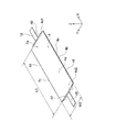
- FIG. 1A is a perspective view of an electric double layer capacitor according to an embodiment of the present invention.
- FIG. 1B is a perspective view of an electric double layer capacitor according to another embodiment of the present invention.
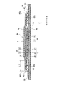
- 2A is a schematic cross-sectional view taken along the line II-II in FIG. 1A.
- FIG. 2B is a schematic cross-sectional view of an electric double layer capacitor according to another embodiment of the present invention.
- FIG. 2C is a schematic cross-sectional view of an electric double layer capacitor according to still another embodiment of the present invention.
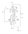
- FIG. 3 is a schematic perspective view showing an example of a manufacturing method of the electric double layer capacitor shown in FIG.
- FIG. 4A is a perspective view showing a continuation process of FIG.
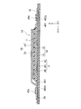
- FIG. 4B is a schematic cross-sectional view taken along line IVB-IVB in FIG. 4A.
- FIG. 5A is a perspective view showing a step subsequent to FIG. 4B.
- FIG. 5B is a perspective view corresponding to FIG. 5A showing a manufacturing method according to another embodiment of the present invention.
- FIG. 6 is a perspective view showing a step subsequent to FIG. 5A or 5B.
- FIG. 7 is a perspective view of an electric double layer capacitor according to another embodiment of the present invention.
- FIG. 8 is a cross-sectional view of an essential part taken along line VIII-VIII in FIG.
- FIG. 9 is a schematic perspective view showing an example of a manufacturing method of the electric double layer capacitor shown in FIG.
- FIG. 10 is a perspective view showing a step subsequent to FIG.
- an electric double layer capacitor (EDLC) 2 as an electrochemical device has an exterior sheet 4.
- the exterior sheet 4 has a front surface 4a and a back surface 4b formed by folding a single sheet 4 around the peripheral edge 4c.
- the exterior sheet 4 has a rectangular shape in which the length L0 in the X-axis direction is longer than the length W0 in the Y-axis direction, but is not limited thereto, and is a square or other polygonal shape, Alternatively, it may be circular, elliptical, or other shapes.
- the direction in which the front surface 4a and the back surface 4b of the exterior sheet 4 overlap is the thickness direction (Z-axis direction), and the directions orthogonal to each other are the X-axis and Y-axis.
- the exterior sheet 4 has a built-in element body 10 as will be described later with reference to FIG. 2A.
- a pair of lead terminals 18, 28 drawn from the element body 10 are drawn on the support sheets 4 f 1 and 4 f 2 outside the exterior sheet 4.
- the interior of the rectangular exterior sheet 4 includes a first seal part 40, a second seal part 42, and a third seal part formed along the four sides of the exterior sheet 4. 44 and the fourth seal portion 46 are hermetically sealed.
- a portion that seals the peripheral edge portion 4d1 of the exterior sheet 4 from which the lead terminal 18 is pulled out in the X-axis direction is referred to as a first seal portion 40.
- a portion that seals the peripheral edge portion 4d2 of the exterior sheet 4 from which the lead terminal 28 is drawn out in the X-axis direction is defined as a second seal portion 42.
- the first seal part 40 and the second seal part 42 are located on the opposite side of the exterior sheet 4 in the X-axis direction.
- a portion that seals the peripheral edge portion 4c formed by folding the exterior sheet 4 is referred to as a third seal portion 44, and a portion that seals the side peripheral edge portion 4e of the exterior sheet 4 located on the opposite side in the Y-axis direction is the first seal portion 44. 4 seals.
- an element body 10 is built in the exterior sheet 4.
- the element body 10 constitutes an element of an electric double layer capacitor.
- a single capacitor element is accommodated in the exterior sheet 4.
- first internal electrodes 16 and second electrodes 26 are laminated so as to sandwich the separator sheet 11 infiltrated with the electrolyte solution.
- One of the first internal electrode 16 and the second internal electrode 26 is a positive electrode and the other is a negative electrode, but the configuration is the same.
- the first internal electrode 16 and the second internal electrode 26 have a first active layer 12 and a second active layer 22 that are laminated so as to be in contact with the opposite surfaces of the separator sheet 11, respectively.
- the first internal electrode 16 and the second internal electrode 26 include a first current collector layer 14 and a second current collector layer 24 that are stacked so as to be in contact with the active layers 12 and 22, respectively.
- the separator sheet 11 is configured to electrically insulate the internal electrodes 16 and 18 and to allow the electrolyte solution to permeate, for example, an electrically insulating porous sheet.
- the electrically insulating porous sheet is at least selected from the group consisting of monolayers and laminates of films made of polyethylene, polypropylene or polyolefin, stretched films of the above-mentioned resin mixtures, or cellulose, polyester and polypropylene. Examples thereof include a fiber nonwoven fabric made of one kind of constituent material.
- the thickness of the separator sheet 11 is, for example, about 5 to 50 ⁇ m.
- the current collector layers 14 and 24 are not particularly limited as long as they are generally highly conductive materials, but metal materials having low electrical resistance are preferably used. For example, sheets of copper, aluminum, nickel, and the like are used. Used. Each of the current collector layers 14 and 24 has a thickness of about 15 to 100 ⁇ m, for example.
- the active layers 12 and 22 include an active material and a binder, and preferably include a conductive aid.
- the active layers 12 and 22 are formed by being laminated on the surfaces of the sheets constituting the current collector layers 14 and 24, respectively.
- the active material examples include porous bodies having various electronic conductivity, such as activated carbon, natural graphite, artificial graphite, mesocarbon microbeads, mesocarbon fiber (MCF), cokes, glassy carbon, and organic compound firing. And carbon materials such as body.
- the binder is not particularly limited as long as the above active material, preferably the conductive auxiliary agent, can be fixed to the sheet constituting the current collector layer, and various binders can be used.
- binder examples include fluorine resins such as polyvinylidene fluoride (PVDF) and polytetrafluoroethylene (PTFE), styrene-butadiene rubber (SBR) and water-soluble polymers (carboxymethylcellulose, polyvinyl alcohol, sodium polyacrylate, Dextrin, gluten, etc.) and the like.
- PVDF polyvinylidene fluoride
- PTFE polytetrafluoroethylene
- SBR styrene-butadiene rubber
- water-soluble polymers carboxymethylcellulose, polyvinyl alcohol, sodium polyacrylate, Dextrin, gluten, etc.
- the conductive additive is a material added to increase the electronic conductivity of the active layers 12 and 22.
- the conductive aid include carbon materials such as carbon black and acetylene black, fine metal powders such as copper, nickel, stainless steel, and iron, a mixture of carbon materials and fine metal powders, and conductive oxides such as ITO.
- each of the active layers 12 and 22 is preferably about 1 to 100 ⁇ m, for example.
- the active layers 12 and 22 are formed on the surfaces of the current collector layers 14 and 24 on the surfaces of the current collector layers 14 and 24 so as to have an area equal to or smaller than that of the separate layer 11.
- the active layers 12 and 22 can be produced by a known method.
- the “positive electrode” is an electrode that adsorbs anions in the electrolyte solution when a voltage is applied to the electric double layer capacitor
- the “negative electrode” is a voltage applied to the electric double layer capacitor.
- the electrode adsorbs cations in the electrolyte solution.
- charging is usually performed in the same direction as the first and charged by applying a voltage in the opposite direction. There is little to do.
- the exterior sheet 4 is made of a material that does not allow the electrolyte solution to be described later to pass therethrough. Further, the outer periphery of the exterior sheet 4 or the sealing tape 40a shown in FIG. It is preferable that they are integrated.
- the sealing tape 40a is preferably a tape-like tape such as an adhesive tape from the viewpoint of workability. However, not only the tape but also a sealant resin that can be applied may be in any form as long as it can be melted and adhered by heat.
- the exterior sheet 4 is configured to seal the element body 10 and prevent air and moisture from entering the sheet 4.
- the exterior sheet 4 may be a single layer sheet, but as shown in FIG. 2A, the exterior sheet 4 is a multilayer sheet in which the metal sheet 4A is laminated so as to be sandwiched between the inner layer 4B and the outer layer 4C. Is preferred.
- the metal sheet 4A is preferably made of, for example, stainless steel, and the inner layer 4B is made of an electrically insulating material, and is similar to a partition sheet such as polypropylene that hardly reacts with the electrolyte solution and can be heat sealed. It is preferable that it is made of a material.
- the outer layer 4C is not particularly limited, and is preferably composed of, for example, PET, PC, PES, PEN, PI, fluororesin, PE, polybutylene terephthalate (PBT), and the like.
- the thickness of the exterior sheet 4 is preferably 5 to 80 ⁇ m.
- the proof stress of the exterior sheet 4 is 390 to 1275 N / mm 2 , preferably 785 to 980 N / mm 2 in JIS Z2241.
- the hardness of the exterior sheet is 230 to 480, preferably 280 to 380 in Picker's hardness (Hv) (JIS 2244).
- the metal sheet 4A of the exterior sheet 4 is made of stainless steel SUS304 (BA), SUS304 (1 / 2H), SUS304 (1 / 2H), SUS304 H, SUS301 BA, SUS301 (1) defined by JIS. / 2H) and SUS301 (3 / 4H) are preferable.
- the lead terminals 18 and 28 are conductive members serving as current input / output terminals for the current collector layers 14 and 24, and have a rectangular plate shape.
- each of the lead terminals 18 and 28 is formed by a sheet integrated with a conductive sheet that constitutes the current collector layers 14 and 24, respectively, and has the same thickness as the current collector layers 14 and 24. There may be.
- the lead terminals 18 and 28 may be formed of a conductive member different from the current collector layers 14 and 24 and electrically connected to the current collector layers 14 and 24. In this case, the thickness of each lead terminal 18 and 28 can be different from the thickness of the current collector layers 14 and 24, for example, about 20 to 100 ⁇ m.
- a space for sealing the element body 10 by the seal portions 40, 42, 44, and 46 sandwiched between the exterior sheets 4 is filled with an electrolyte solution (not shown), and part of the active layers 12, 22.
- the separator sheet 11 is impregnated.
- the electrolyte solution a solution in which an electrolyte is dissolved in an organic solvent is used.
- the electrolyte include quaternary ammonium salts such as tetraethylammonium tetrafluoroborate (TEA + BF4 ⁇ ) and triethylmonomethylammonium tetrafluoroborate (TEMA + BF4 ⁇ ), ammonium salts, amine salts, amidine salts, and the like. Is preferred.
- these electrolytes may be used individually by 1 type, and may use 2 or more types together.
- organic solvent a known solvent can be used.
- Preferred examples of the organic solvent include propylene carbonate, ethylene carbonate, dimethyl carbonate, methyl ethyl carbonate, diethyl carbonate, ⁇ -butyrolactone, dimethylformamide, sulfolane, acetonitrile, propionitrile, and methoxyacetonitrile. These may be used alone or in combination of two or more at any ratio.
- first seal portion 40 and the second seal portion 42 are portions from which the lead terminals 18 and 28 are drawn to the outside, and are particularly required to have a sealing performance as compared with the third seal portion 43 and the fourth seal portion 44.
- each of the lead terminals 18 and 28 shown in FIGS. 3 and 4 may be the same or different.
- the width of the lead terminals 18 and 28 in the Y-axis direction is Y of the current collector layers 14 and 24.
- it may be substantially the same as the axial width W1 (see FIG. 4), it may be smaller or larger than the width W1.
- the width W1 in the Y-axis direction of the current collector layers 14, 24 is preferably 2 to 10 mm, preferably smaller than the width W3 in the Y-axis direction of the separator sheet 11, and W3-W1 is preferably 0.2 to 2 mm.
- the current collector layers 14 and 24 are preferably disposed in the center of the separator sheet 11 in the Y-axis direction.
- the width W0 in the Y-axis direction of the EDLC 2 shown in FIG. 1 is preferably 10 to 50 mm when accommodated in the IC card, and the length of the EDLC 2 in the X-axis direction excluding the lead terminals 18 and 28 is L0 is preferably 10 to 50 mm.
- the first seal portion 40 and the second seal portion 42 include sealing tapes 40a and 42a and peripheral portions 4d1 and 4d2 of the exterior sheet 4 as shown in FIGS. It is formed integrally by heating at the time of heat sealing. At that time, as shown in FIG. 2A, a part of the inner layer (resin) 4B formed on the inner peripheral surface of the exterior sheet 4 is brought into close contact with the one side surfaces of the lead terminals 18 and 28, and heat It becomes welding part 4Ba and the sealing performance in the 1st seal part 40 and the 2nd seal part 42 is improved.
- the inner layer 4B of the exterior sheet 4 is fused and integrated by being folded at the folded peripheral edge portion 4c of the exterior sheet 4 and heated during heat sealing.
- the inner layers 4B of the side peripheral edge portions 4e on the front surface 4a and the back surface 4b of the exterior sheet 4 are fused and integrated by heating during heat sealing.
- one end of the third seal portion 44 and the fourth seal portion 46 is continuously formed so as to be connected, respectively.
- the second seal portion 42 is formed continuously so as to connect the other end of the four seal portion 46. Therefore, the inside of the exterior sheet 4 is well sealed against the outside of the exterior sheet 4.
- the first lead terminal 18 and the second lead terminal 28 of the element body 10 are drawn out to the opposite side along the longitudinal (X-axis direction) direction of the EDLC 2. Therefore, the width of the EDLC 2 in the Y-axis direction can be reduced, the thicknesses of the first seal portion 40 and the second seal portion 42 can be minimized, and the overall thickness of the EDLC 2 can be reduced. . For this reason, size reduction and thickness reduction of EDLC2 are realizable.
- the first lead terminal 18 is a positive electrode and the second lead terminal 28 is a negative electrode, which is connected to the element body 10 immersed in an electrolyte solution.
- the withstand voltage of a single element is determined to be about 2.85 V at maximum, and the elements may be connected in series in order to improve the withstand voltage according to the application. Since the EDLC 2 of the present embodiment is extremely thin and has a sufficient withstand voltage, it can be suitably used as a battery for incorporation in a thin electronic component such as an IC card.
- the element body 10 is first manufactured.
- one electrode 16 is prepared, and a tape 40 a is attached to a boundary portion between the electrode 16 and the lead terminal 18. And the electrode 16 and the tape 40a are fixed to the predetermined position of the sheet
- seat 4 so that the active layer 12 of the electrode 16 may face the upper direction of a Z-axis.
- the tip of a spot heat welding tool (not shown) is applied to the intersection of the tape 40a and the electrode 16 (the portion where the active layer 12 is not formed), and the tape 40a and the electrode 16 are placed on the inner surface of the sheet 4.
- the resin inner layer 4B is partially heat-sealed.
- the inner layer 4B made of resin is partially melted at the position corresponding to the intersection of the tape 40a and the electrode 16 (the first current collector layer 14 where the active layer 12 is not formed).
- a landing portion 4B2a is formed.
- the shape of the electrode fusion part 4B2a that is partially formed is not particularly limited.
- the outer diameter is a circle having a diameter of about 0.2 to 1.0 mm, an elliptical shape having the same size, or a similar size.
- the electrode fusion part 4B2a fixes the electrode 16 and the tape 40a to the resin inner layer 4B of the exterior sheet 4 at a predetermined position.
- the separator sheet 11 is attached so as to cover the active layer 12 of the electrode 16, and as shown in FIG. 4A, spot heat welding is performed on the four corners of the separator sheet 11 (parts not overlapping with the electrode 16). Touch the tip of a tool (not shown).
- the separator sheet 11 is partially heat-sealed to the resin-made inner layer 4B of the exterior sheet 4, and the resin-made inner layer 4B is partially covered at positions corresponding to the corners of the separator sheet 11.
- the separator fused portion 4B1 is formed on the substrate.
- the shape and size of the separator fusion part 4B1 are the same as those of the electrode fusion part 4B2a.
- the separator fusion portion 4B1 fixes the separator sheet 11 to the resin inner layer 4B of the exterior sheet 4 at a predetermined position.
- the other electrode 26 is prepared, and a tape 42 a is attached to the boundary portion between the electrode 26 and the lead terminal 28. Then, the electrode 26 and the tape 42a are disposed at predetermined positions on the sheet inner layer 4B that becomes the back surface 4b of the exterior sheet 4 so that the active layer 22 of the electrode 26 faces downward in the Z-axis direction (side facing the separator sheet 11). And fix. As shown in FIG. 4B, it is preferable that the active layer 22 of the electrode 26 is accurately aligned and faced with the active layer 22 of the electrode 16 with the separator sheet 11 interposed therebetween.
- the tip of the spot heat welding tool (not shown) is applied to the intersection of the tape 42a and the electrode 26 (the portion where the active layer 22 is not formed), and the tape 42a and the electrode 26 is partially heat-sealed to the resin inner layer 4B formed on the inner surface of the sheet 4.
- the resin inner layer 4B is partially used as an electrode at a position corresponding to the intersection of the tape 42a and the electrode 26 (the portion where the active layer 22 is not formed). Fusion part 4B2b is formed.
- the shape and size of the electrode fusion part 4B2b formed partially are the same as those of the electrode fusion part 4B2a.
- the electrode fusion part 4B2b fixes the electrode 26 and the tape 42a to the resin inner layer 4B of the exterior sheet 4 at a predetermined position.
- the internal electrodes 16 and 26 are laminated on both sides of the separator sheet 11 so that the active layers 12 and 22 are positioned and in contact with each other.
- Sealing tapes 40a and 42a are attached to the lead terminals 18 and 28 only on one side surfaces of the terminals 18 and 28, respectively, in the X-axis direction positions to be the first seal portion 40 and the second seal portion 42 described above. (See FIG. 4B).
- the sealing tapes 40a and 42a are bonded to only one side surface of each of the terminals 18 and 28. However, as shown in FIG. , 28 may be adhered to both sides.
- the width W2 (see FIG. 4A) of the tapes 40a and 42a in the Y-axis direction is preferably longer than the width of the lead terminals 18 and 28 in the Y-axis direction by about 0.5 to 3 mm.
- the width in the Y-axis direction of the tapes 40a and 42a corresponds to the width in the Y-axis direction of the first seal portion 40 and the second seal portion 42 of the EDLC2 shown in FIG. 1, and defines the Y-axis direction width W0 of the EDLC2. .
- the width W2 in the Y-axis direction of the tapes 40a and 42a shown in FIG. 4A is too narrow, the sealing performance in the first seal part 40 and the second seal part 42 shown in FIG. 1A may not be sufficient, and the width is wide. If too large, the Y-axis direction width W0 of the EDLC 2 becomes larger than necessary.
- the width in the X-axis direction of the tapes 40a and 42a corresponds to the length L1 in the X-axis direction of the first seal portion 40 and the second seal portion 42 shown in FIG. 2, and is preferably 2 to 4 mm.
- the exterior sheet 4 is folded back at the peripheral edge 4 c so as to cover the entire element body 10, and the element body 10 is covered with the front surface 4 a and the back surface 4 b of the sheet.
- the exterior sheet 4 is formed long in advance in the Y-axis direction.
- the width in the X-axis direction on the surface 4a of the exterior sheet 4 is such that the peripheral edge 4d1 on the first seal portion side of the exterior sheet 4 overlaps with the tape 40a, and the peripheral edge 4d2 on the second seal portion side of the exterior sheet 4 is the tape 42a. It has been adjusted to overlap.
- the exterior sheet 4 that covers the entire element body 10 is set in a jig (not shown), the folded peripheral edge 4 c of the exterior sheet 4 is heated under pressure, and the third seal A portion 44 is formed.
- the peripheral edge 4d1 on the first seal part side and the peripheral edge 4d2 on the second seal part side of the exterior sheet are pressurized and heated to form the first seal part 40 and the second seal part 42.
- a part of the inner layer (resin) 4B formed on the inner peripheral surface of the lower exterior sheet 4 is formed on one side surface (lower surface) of the lead terminals 18 and 28.
- the sealing tapes 40a and 42a attached to the other one-side surface (upper surface) of the lead terminals 18 and 28 are used as an adhesive resin that flows by pressurization and heating, and the inner layer 4B of the exterior sheet 4
- the seal portions 40 and 42 are integrated after close contact and solidified.
- the sealing tapes 40a and 42a are adhesive resins that flow by pressurization and heating, and the portions 40b and 42b protrude outward from the peripheral edge of the exterior sheet 4 located on the upper side. The edge of the peripheral edge of the sheet 4 is covered.
- an electrolyte solution is injected from the opening end 52 of the exterior sheet 4 where the fourth seal portion 46 is not formed, and then the last fourth seal portion 46 is similar to the above. Formed by heat sealing. Thereafter, the exterior sheet 4 is cut along the cutting line 54 outside the fourth seal portion 46, and the excess exterior sheet 4 'is removed, whereby the EDLC 2 of the present embodiment is obtained.
- the first sealing portion 40 has a sealing tape 40a attached to one surface of the first lead terminal 18 at the peripheral portion 4d1 on the first sealing portion side of the upper exterior sheet 4, and is heated. It is formed by sealing (thermocompression bonding).
- the first seal portion 40 includes a thermocompression bonding portion 4Ba formed on a part of the resin inner layer 4B formed on the inner surface of the lower exterior sheet 4.
- the sealing tape 42 a attached to one surface of the second lead terminal 28 is a peripheral portion 4 d 2 on the second seal portion side of the upper exterior sheet 4, and heat is applied. It is formed by sealing (thermocompression bonding).
- the second seal portion 42 includes a thermocompression bonding portion 4Ba formed on a part of the resin inner layer 4B formed on the inner surface of the lower exterior sheet 4.
- insulating tape 40a, 42a for constituting a seal part is functioned as an adhesive resin only on one side surface (upper surface) of the lead terminals 18, 28, and the other surface (lower surface) is
- the heat-sealed portion 4Ba is formed by directly contacting the resin inner layer 4B formed on the inner surface of the exterior sheet 4.
- the electrochemical device is thinned to such a level that it can be incorporated in a thin electronic device such as an IC card while ensuring internal sealing and avoiding a short circuit. Is possible.
- a part of the adhesive resin constituting the seal portions 40 and 42 protrudes outward from the peripheral edge of the upper exterior sheet 4 and covers the edge of the peripheral edge of the exterior sheet 4. Yes. Therefore, there is no possibility that the edge of the metal sheet 4A constituting the exterior sheet 4 is exposed at the edge of the peripheral edge of the exterior sheet 4, and the short circuit between the lead terminals 18 and 28 and the metal sheet 4A is effectively prevented. Can do.
- the device 2 of the present embodiment has the support sheets 4f1 and 4f2 that prevent the lead terminals 18 and 28 drawn from the seal portions 40 and 42 from being bent, the leads drawn from the seal portions 40 and 42 are provided. It is possible to effectively prevent the terminals 18 and 28 from being bent.
- the support sheets 4f1 and 4f2 are configured such that a part of the peripheral edge of the lower exterior sheet 4 positioned at the seal portions 40 and 42 extends outward, it is easy to form the support sheets 4f1 and 4f2. become.
- the protruding lengths of the support sheets 4f1 and 4f2 are longer than the protruding lengths of the lead terminals 18 and 28, it is possible to effectively prevent the bending of the lead terminals 18 and 28 drawn from the seal portions 40 and 42. .
- a separator fusion part 4B1 for partially attaching a part of the separator sheet 11 to the inner surface of the outer sheet 4 is formed on the resin inner layer 4A existing on the inner surface of the outer sheet 4. is there. For this reason, at least the separator sheet 11 is positioned inside the exterior sheet 4, and positioning with the internal electrodes 16 and 26 is facilitated. Conventionally, there is no need to use a positioning tape that remains inside the element 10.
- the device 2 is further thinned while preventing the positional deviation between the separator sheet 11 and the pair of internal electrodes 16 and 26 inside the exterior sheet 4. Is possible.
- the separator fusion part 4B1 is formed on the internal electrodes 16 and 26 because it is partially attached to the corners of the separator sheet 11 that do not overlap with the internal electrodes 16 and 26 when viewed from the Z-axis direction.
- the effective areas of the active layers 12 and 24 are not narrowed, and their functions can be fully exhibited.
- electrode fusion portions 4B2a and 4B2b for partially adhering a part of the internal electrodes 16 and 26, which do not overlap with the separate sheet 11 when viewed from the Z-axis direction, to the inner surface of the exterior sheet 4 are fused for the separator.
- the inner layer 4B is formed separately from the portion 4B1.
- the electrode fusion portions 4B2a and 4B2b are formed at portions that do not overlap with the separate sheet 11 when viewed from the Z-axis direction, the electrode fusion portions 4B2a and 4B2b are formed on the internal electrodes 16 and 26 at positions overlapping the separate sheet 11.
- the functions of the formed active layers 12 and 22 can be sufficiently exhibited.
- the exterior sheet 4 has a front surface 4 a that covers the surface of the element body 10 and a back surface 4 b that covers the back surface of the element body 10, and both of the pair of internal electrodes 16 and 26 are on the back surface 4 b of the exterior sheet 4. It is partially attached to the inner layer 4B via electrode fusion portions 4B2a and 4B2b. Therefore, it becomes possible to position the pair of internal electrodes 16 and 26 and the separate sheet 11 with respect to the back surface 4b of the exterior sheet 4, eliminating the positional displacement between the internal electrodes 16 and 26, and improving the performance of the device. . In addition, it is not necessary to use a positioning tape, which contributes to a thinner device.
- the maximum thickness of the EDLC 2 can be 1 mm or less, preferably 0.9 mm or less, and more preferably 0.5 mm or less.
- the EDLC 2a of this embodiment is the same as the EDLC 2 of the first embodiment except that it does not have the support sheets 4f1 and 4f2 shown in FIG. 1A.
- the heat-resistant insulating layer 50 is formed on the surfaces of the support sheets 4f1 and 4f2 that are in contact with the lead terminals 18 and 28 protruding from the seal portions 40 and 42. They are stacked. With this configuration, even when heat is applied during electrical connection between the lead terminals 18 and 28 and external connection terminals (not shown), the metal sheet 4A existing inside the exterior sheet 4 and the lead terminals 18 and 28 are present. Can be effectively prevented.
- PET polyethylene terephthalate
- nylon, PET, PC, PES, PEN, PI, fluororesin, and the like may be used.
- the seal portions 40 formed on the peripheral portions 4d1, 4d2 of the exterior sheet 4 in which the lead terminals 18, 28 are pulled out to the outside in the X-axis direction.
- Reference numeral 42 denotes a pair of sealing tapes 40a and 40b. That is, a pair of sealing tapes 40a and 40b are provided so as to cover the front and back surfaces with the lead terminals 18 and 28 interposed therebetween, and they are thermocompression bonded to form the seal portions 40 and 42.
- each of the seal portions 40 and 42 is thicker than that of the above-described embodiment, but it is a sufficiently thin level as compared with the prior art. Since other configurations and operational effects of the present embodiment are the same as those of the first to third embodiments, common members are denoted by common reference numerals in the drawings, and description of common portions is omitted.
- the first step is to form a part where the electrode fusion part 4B2a and the separator fusion part 4B1 are partially formed on the inner layer 4B serving as the back surface 4b of the exterior sheet 4.
- the electrode fusion part 4B2b is partially formed on the inner layer 4B that becomes the surface 4a of the exterior sheet 4, and the other electrode 26 and the tape 42a are positioned and fixed.
- the active layer 22 of the other electrode 26 is directed upward in the Z-axis direction so that the current collector layer 24 of the other electrode 26 is in contact with the inner layer 4B of the exterior sheet 4.
- the exterior sheet 4 is folded back at the peripheral edge 4c so as to cover the entire element body 10, and the element body 10 is covered with the front surface 4a and the back surface 4b of the sheet.
- the subsequent steps are the same as those in the first embodiment described above.
- the present embodiment it becomes possible to position the pair of internal electrodes 16 and 26 and the separate sheet 11 with respect to the front surface 4a and the back surface 4b of the exterior sheet 4, and the positional displacement of the internal electrodes 16 and 26 is eliminated. Device performance is improved. In addition, it is not necessary to use a positioning tape, which contributes to a thinner device. Furthermore, in this embodiment, compared to the embodiment shown in FIG. 5A, the inner electrode 26 is fixed to the inner layer 4 ⁇ / b> B of the surface 4 a of the exterior sheet 4 in a flatter state, and thus acts on the inner electrode 26. It is also possible to reduce internal stress.
- FIG. 7 in the EDLC 2 d of this embodiment, two element bodies 10 a and 10 b are built in the exterior sheet 4 side by side in the Y-axis direction.
- the other parts are the same as those in the first embodiment, and therefore, in the drawings, common members are denoted by common reference numerals, and in the following description, description of common parts is omitted, and different parts are described in detail.
- the exterior sheet 4 is composed of a top sheet 4a1 and a back sheet 4b1, and is approximately twice as large in the Y-axis direction as the exterior sheet 4 shown in FIG.
- the exterior sheet 4 is composed of a top sheet 4a1 and a back sheet 4b1, and is approximately twice as large in the Y-axis direction as the exterior sheet 4 shown in FIG.
- two element bodies 10a and 10b are built in the exterior sheet 4, and each of the element bodies 10a and 10b has the same structure as the element body 10 of the first embodiment. have.
- first lead terminals 18 and 18 of the element bodies 10a and 10b are formed separately, but the second lead terminals 28a of the element bodies 10a and 10b are integrally formed with the connecting portion 28b. And they are continuous with each other. That is, as shown in FIG. 9, each element body 10a, 10b is connected to the first lead terminal 18a formed integrally with each first current collector layer 14 of each element body 10a, 10b. They are connected in series via the part 18b.
- a third seal portion 44a is formed along the X-axis direction at the axial central portion of the exterior sheet 4, and the flow of the electrolyte solution is blocked between the element main bodies 10a and 10b. .
- the space in which the element main body 10a is accommodated is sealed by the first seal portion 40, the second seal portion 42, the third seal portion 44a, and the fourth seal portion 46a that are continuously formed on the exterior sheet 4, and the electrolyte solution is Stored.
- the space in which the element body 10b is accommodated is sealed by the first seal portion 40, the second seal portion 42, the third seal portion 44a, and the fourth seal portion 46b that are continuously formed on the exterior sheet 4.
- the electrolyte solution is stored.
- two element bodies 10a and 10b are formed on the pair of separator sheets 11 in the Y-axis direction.
- Two element bodies 10a and 10b may be formed using a single separator sheet 11.
- the manufacturing method of the element bodies 10a and 10b is the same as in the case of the first embodiment.
- Sealing tapes 40a and 42a are adhered to the one-side surfaces of the terminals 18 and 28a on the lead terminals 18 and 28a of the element bodies 10a and 10b, respectively, in the same manner as in the above-described embodiment. Further, the method for forming the electrode fusion portions 4B2a and 4B2b and the separator fusion portion 4B1 is the same as that of the above-described embodiment. In this embodiment, the corner
- the top sheet 4a1 and the back sheet 4b1 constituting the exterior sheet 4 are combined so as to cover the entire element bodies 10a and 10b, and the element bodies 10a and 10b are covered with these.
- the exterior sheet 4 is formed long in advance in the Y-axis direction.
- the width of the exterior sheet 4 in the X-axis direction is such that the peripheral portion 4d1 on the first seal portion side of the exterior sheet 4 overlaps with the tape 40a, and the peripheral portion 4d2 on the second seat portion side of the exterior sheet 4 overlaps with the tape 42a. Have been adjusted so that.
- the exterior sheet 4 that covers the entire element body 10 is set in a jig (not shown), and the center portion of the exterior sheet 4 in the Y-axis direction extends along the X-axis direction.
- the third seal portion 44a is formed by pressurizing and heating.
- the peripheral edge 4d1 on the first seal part side of the exterior sheet and the peripheral edge 4d2 on the second seal part side are heated under pressure to form the first seal part 40 and the second seal part 42.
- an electrolyte solution is injected from the open end 52 of the exterior sheet 4 where the fourth seal portions 46a and 46b are not formed, and then the last fourth seal portions 46a and 46b are heat sealed as described above. To form. Thereafter, the exterior sheet 4 is cut along the cutting line 54 outside the fourth seal portions 46a and 46b, and the excess exterior sheet 4 ′ is removed, whereby the EDLC 2d of the present embodiment shown in FIG. 7 is obtained. .
- the lead terminal 18a drawn from one side of the exterior sheet 4 in the X-axis direction is integrally connected in advance by the connecting portion 18b.
- the lead terminal 18a not having the connecting portion 18b is connected.
- Each may be pulled out from the first seal portion 40.
- the laminate type electrochemical device to which the present invention is applied is not limited to EDLC, but can be applied to lithium batteries, lithium battery capacitors, and the like.
Landscapes
- Engineering & Computer Science (AREA)
- Chemical & Material Sciences (AREA)
- Chemical Kinetics & Catalysis (AREA)
- Electrochemistry (AREA)
- General Chemical & Material Sciences (AREA)
- Power Engineering (AREA)
- Manufacturing & Machinery (AREA)
- Microelectronics & Electronic Packaging (AREA)
- Electric Double-Layer Capacitors Or The Like (AREA)
- Sealing Battery Cases Or Jackets (AREA)
- Secondary Cells (AREA)
- Cell Separators (AREA)
- Battery Mounting, Suspending (AREA)
- Connection Of Batteries Or Terminals (AREA)
Abstract
【課題】ICカードなどの薄型電子機器内にも内蔵することが可能なレベルにまで薄型が可能な電気化学デバイスおよびその製造方法を提供すること。 【解決手段】セパレータシート11を挟むように一対の内部電極16,26が積層してある素子本体10と、素子本体10を覆う外装シート4と、素子本体10が電解質溶液で浸漬されるように、外装シート4の周縁部を密封するシール部40,42と、いずれかの内部電極16,26に電気的に接続してあり、外装シート4のシール部40,42から外側に引き出されるリード端子18,28と、を有する電気化学デバイスである。セパレータシート11の一部を外装シート4の内面に部分的に付着させるセパレータ用融着部4B1が、外装シート4の内面に存在する樹脂製の内側層4Bに形成してある。
Description
本発明は、電気二重層キャパシタ(EDLC)などとして好ましく用いられる電気化学デバイスおよびその製造方法に関する。
昨今、ICチップを搭載するICカードの普及には目を見張るものがある。特に金銭のやり取りを行うことも可能なICカードもあり、社員証や会員証など、さまざまな用途に使われ、今後さらにICカードの高機能化の対応が求められている。
高機能化に伴い、従来ICカードに使われる蓄電池は、出来るだけ高容量の一次電池を用いることが検討されている。しかしながら、1次電池では、蓄積容量がなくなるとカードを交換しなくてはならない。そこで、充電可能な2次電池を用いたICカードの開発が進んでいる。
ICカード用の2次電池の特性として、カード厚み以下の薄型、カード内蔵可能な小型、折り曲げに対応したフレキシブル性が求められている。一方で、ICカード内部に蓄電システムを持たず、カードリーダーを通しての比接触で得られる電力を用いて通信を行うシステムの開発も進んでいる。
しかしながら、非接触充電で得られた電力は僅かであることから、高機能な製品では十分な電力を得ることができない。そこで、充電ロスが少なく、短時間で充電でき、かつ回路の動作電圧まで充電できる二次電池が必要となってきている。
従来の電気化学デバイスでは、蓄電容量が大きいために、カードリーダーにて十分な電圧を送ることができない。そこで低容量で的確な抵抗を持つEDLCが必要となってきている。このときICカード内での電池製品の厚みは、たとえば1.0mm以下、好ましくは0.9mm以下、さらに好ましくは0.5mm以下と、非常に薄いことを要求される。また、カード内への収容面積サイズも限られている。
たとえば特許文献1などに示す従来のEDLCは、外装シートの内部に、一対の内部電極がセパレータを挟む積層構造を有しているが、セパレータを挟んで配置される内部電極が向き合うように位置合わせする必要がある。そのため、従来では、絶縁テープなどを用いて、一対の内部電極とセパレータとを相互に貼り付けて位置合わせしている。位置合わせ後に、外装シートの内部を密封することから、位置合わせ用の絶縁テープは、外装シートの内部に残った状態となる。そのため、従来では、位置合わせ用の絶縁テープの分だけ厚みが大きくなり、EDLCを、必要とされる水準までに十分に薄くすることを困難にしていた。
本発明は、このような実状に鑑みてなされ、その目的は、ICカードなどの薄型電子機器内にも内蔵することが可能なレベルにまで薄型が可能な電気化学デバイスおよびその製造方法を提供することである。
上記目的を達成するために、本発明に係る電気化学デバイスは、
セパレータシートを挟むように一対の内部電極が積層してある素子本体と、
前記素子本体を覆う外装シートと、
前記素子本体が電解質溶液で浸漬されるように、前記外装シートの周縁部を密封するシール部と、
いずれかの前記内部電極に電気的に接続してあり、前記外装シートの前記シール部から外側に引き出されるリード端子と、を有する電気化学デバイスであって、
前記セパレータシートの少なくとも一部を前記外装シートの内面に付着させるセパレータ用融着部が、前記外装シートの内面に存在する樹脂製の内側層に形成してあることを特徴とする。
セパレータシートを挟むように一対の内部電極が積層してある素子本体と、
前記素子本体を覆う外装シートと、
前記素子本体が電解質溶液で浸漬されるように、前記外装シートの周縁部を密封するシール部と、
いずれかの前記内部電極に電気的に接続してあり、前記外装シートの前記シール部から外側に引き出されるリード端子と、を有する電気化学デバイスであって、
前記セパレータシートの少なくとも一部を前記外装シートの内面に付着させるセパレータ用融着部が、前記外装シートの内面に存在する樹脂製の内側層に形成してあることを特徴とする。
本発明では、セパレータシートの一部を前記外装シートの内面に付着させるセパレータ用融着部が、外装シートの内面に存在する樹脂製の内側層に形成してある。このため、少なくとも、セパレータシートが外装シートの内部で位置決めされ、内部電極との位置決めが容易になり、位置決め用テープを用いる必要がなくなる。
すなわち、本発明に係る電気化学デバイスでは、外装シートの内部でのセパレータシートと一対の内部電極との位置ズレを防止しながら、デバイスの厚みを1mm以下、好ましくは0.9mm以下、さらに好ましくは0.5mm以下にすることができる。その結果、たとえばICカードなどの薄型電子機器内にも内蔵することが可能なレベルにまで電気化学デバイスの薄型化が可能である。
好ましくは、前記セパレータ用融着部は、前記内部電極とは重複しない前記セパレータシートの一部に付着してある。このように構成することで、内部電極に形成してある活性層の機能を十分に発揮させることができる。
好ましくは、前記セパレートシートとは重複しない前記内部電極の一部を前記外装シートの内面に付着させる電極用融着部が、前記セパレータ用融着部とは別に前記内側層に形成してある。このように構成することで、内部電極も外装シートの内面に固定されて位置決めされる。このため、セパレータシートに対する一対の内部電極の位置決めが容易になり、位置決め用テープを用いる必要がなくなり、デバイスの薄層化に寄与する。
また、電極用融着部は、セパレートシートとは重複しない部分に形成してあるために、セパレートシートに重複してある位置で内部電極に形成してある活性層の機能を十分に発揮させることができる。
好ましくは、前記外装シートは、前記素子本体の表面を覆う表面部と、前記素子本体の裏面を覆う裏面部とを有し、
前記一対の内部電極の双方が、前記表面部または前記裏面部の内のいずれか一方の内面に、前記電極用融着部を介して付着してある。
前記一対の内部電極の双方が、前記表面部または前記裏面部の内のいずれか一方の内面に、前記電極用融着部を介して付着してある。
このように構成することで、外装シートの表面部または裏面部に対して、一対の内部電極およびセパレートシートを位置決めすることが可能になり、内部電極の位置ズレが無くなり、デバイスの性能が向上する。また、位置決め用テープを用いる必要がなくなり、デバイスの薄層化に寄与する。
あるいは、前記外装シートは、前記素子本体の表面を覆う表面部と、前記素子本体の裏面を覆う裏面部とを有し、
前記一対の内部電極の一方が、前記表面部または前記裏面部の内のいずれか一方の内面に、前記電極用融着部を介して付着してあり、
前記一対の内部電極の他方が、前記表面部または前記裏面部の内のいずれか他方の内面に、前記電極用融着部を介して付着してあっても良い。
前記一対の内部電極の一方が、前記表面部または前記裏面部の内のいずれか一方の内面に、前記電極用融着部を介して付着してあり、
前記一対の内部電極の他方が、前記表面部または前記裏面部の内のいずれか他方の内面に、前記電極用融着部を介して付着してあっても良い。
このように構成することで、外装シートの表面部および裏面部に対して、一対の内部電極およびセパレートシートを位置決めすることが可能になり、内部電極の位置ズレが無くなり、デバイスの性能が向上する。また、位置決め用テープを用いる必要がなくなり、デバイスの薄層化に寄与する。
好ましくは、前記外装シートの前記シール部から外側に引き出される前記リード端子の一方の面が、前記シール部に位置して前記外装シートの内面に形成してある樹脂製の内側層に直接に接触している。
従来では、密封性を確保すると共に短絡を回避するためには、リード端子の両面に、シール部を構成するための絶縁テープを貼り付けて接着用樹脂を両面に具備させる必要があると考えられていた。しかしながら、本発明者等の鋭意研究の結果、リード端子の片側の面のみにシール部を構成するための絶縁テープを貼り接着用樹脂として機能させ、他の面は、外装シートの内面に形成してある樹脂製の内側層に直接に接触させて融着することにより、密封性を確保すると共に短絡を回避することができることが初めて見出された。その結果、密封性を確保すると共に短絡を回避しながら、最も厚みが厚くなる部分であるシール部の厚みを極限にまで薄くすることに成功した。
すなわち、この電気化学デバイスでは、内部の密封性を確保すると共に短絡を回避しながら、デバイスの厚みを、さらに薄くすることが可能である。
好ましくは、前記外装シートの前記シール部から外側に引き出される前記リード端子の他方の面には、前記外装シートの内面に形成してある樹脂製の内側層と接触する接着用樹脂を介して前記外装シートの周縁部が接着してあり、
前記接着用樹脂の一部は、前記外装シートの周縁部から外側にはみ出して、当該外装シートの周縁部の縁端を覆っている。
前記接着用樹脂の一部は、前記外装シートの周縁部から外側にはみ出して、当該外装シートの周縁部の縁端を覆っている。
外装シートとしては、金属シートの両面が絶縁層で覆われたシートか好ましく用いられる。外装シートの周縁部の縁端では、金属シートの端部が露出するおそれがあり、その露出した金属シートが、リード端子と接触すると、短絡の原因になる。本発明の好ましい態様では、シール部を構成する接着用樹脂の一部は、外装シートの周縁部から外側にはみ出して、当該外装シートの周縁部の縁端を覆っている。そのため、外装シートの周縁部の縁端では、外装シートを構成する金属シートの端が露出するおそれが無くなり、リード端子と金属シートとの短絡などを有効に防止することができる。
本発明の電気化学デバイスは、前記シール部から引き出された前記リード端子の折れ曲がりを防止するサポートシートをさらに有してもよい。このように構成することで、シール部から引き出されたリード端子の折れ曲がりを有効に防止することができる。
好ましくは、前記サポートシートは、前記シール部に位置する前記外装シートの周縁部の一部が外側に延長して構成されている。このように構成することで、サポートシートの形成が容易になる。
前記サポートシートの突出長さは、前記リード端子の突出長さよりも長くてもよい。このように構成することで、シール部から引き出されたリード端子の折れ曲がりを有効に防
止することができる。
止することができる。
シール部から飛び出している前記リード端子と接触する前記サポートシートの面には、耐熱絶縁層が積層してあってもよい。このように構成することで、リード端子と外部接続端子との電気接続時に熱が加わっても、外装シートの内部に存在する金属シートと、リード端子との短絡を、有効に防止することができる。
上記のいずれかの本発明に係る電気化学デバイスの製造方法は、
いずれか一方の前記内部電極を、前記外装シートの内面に部分的に融着させる工程と、
前記内部電極の活性層を覆うように、前記セパレータシートを前記外装シートの内面に部分的に融着させる工程と、
前記セパレータシートの上に、いずれか他方の前記内部電極が配置されるように、そのいずれか他方の前記内部電極を、前記外装シートの内面に部分的に融着させる工程と、
前記素子本体を覆うように、前記外装シートで覆う工程と、
前記素子本体が電解質溶液で浸漬されるように、前記外装シートの周縁部を密封する工程と、を有する。
いずれか一方の前記内部電極を、前記外装シートの内面に部分的に融着させる工程と、
前記内部電極の活性層を覆うように、前記セパレータシートを前記外装シートの内面に部分的に融着させる工程と、
前記セパレータシートの上に、いずれか他方の前記内部電極が配置されるように、そのいずれか他方の前記内部電極を、前記外装シートの内面に部分的に融着させる工程と、
前記素子本体を覆うように、前記外装シートで覆う工程と、
前記素子本体が電解質溶液で浸漬されるように、前記外装シートの周縁部を密封する工程と、を有する。
好ましくは、前記リード端子が引き出される前記シール部は、前記外装シートの間に挟まれる密封用テープが加熱加圧されることで形成され、
前記密封用テープは、加熱加圧される前に、前記内部電極と共に、前記外装シートの内面に部分的に融着される。
前記密封用テープは、加熱加圧される前に、前記内部電極と共に、前記外装シートの内面に部分的に融着される。
以下、本発明を、図面に示す実施形態に基づき説明する。
第1実施形態
図1Aに示すように、本発明の一実施形態に係る電気化学デバイスとしての電気二重層キャパシタ(EDLC)2は、外装シート4を有する。外装シート4には、一枚のシート4を折り返し周縁部4cで折り曲げて表面4aおよび裏面4bが形成してある。
図1Aに示すように、本発明の一実施形態に係る電気化学デバイスとしての電気二重層キャパシタ(EDLC)2は、外装シート4を有する。外装シート4には、一枚のシート4を折り返し周縁部4cで折り曲げて表面4aおよび裏面4bが形成してある。
本実施形態では、外装シート4は、X軸方向の長さL0がY軸方向の長さW0に比較して長い長方形状を有するが、これに限定されず、正方形でも、その他の多角形状、あるいは円形、楕円形、あるいはその他の形状でも良い。この実施形態では、外装シート4の表面4aと裏面4bとが重なる方向を厚み方向(Z軸方向)とし、それに相互に直交する方向をX軸およびY軸とする。
外装シート4には、図2Aを用いて後述するように、素子本体10が内蔵してある。素子本体10から引き出される一対のリード端子18,28が、外装シート4の外部で、サポートシート4f1および4f2の上に引き出されている。
図1Aに示すように、本実施形態では、長方形状の外装シート4の内部は、外装シート4の四辺に沿って形成してある第1シール部40、第2シール部42、第3シール部44および第4シール部46とに囲まれて密封してある。
この実施形態では、リード端子18がX軸方向の外側に引き出される外装シート4の周縁部4d1を密封する部分を第1シール部40とする。また、リード端子28がX軸方向の外側に引き出される外装シート4の周縁部4d2を密封する部分を第2シール部42とする。第1シール部40と第2シール部42とは、外装シート4のX軸方向の反対側に位置する。また、外装シート4を折り返してなる周縁部4cを密封する部分を第3シール部44とし、そのY軸方向の反対側に位置する外装シート4のサイド周縁部4eを密封している部分を第4シール部とする。
図2Aに示すように、外装シート4の内部には、素子本体10が内蔵してある。素子本体10は、電気二重層キャパシタの素子を構成しており、本実施形態では、単一のキャパシタ素子が外装シート4の内部に収容してある。
素子10では、電解質溶液が染み込んであるセパレータシート11を挟むように一対の第1内部電極16と第2電極26とが積層してある。第1内部電極16と第2内部電極26のうちの一方は、正極となり、他方は、負極となるが、構成は同じである。これらの第1内部電極16および第2内部電極26は、それぞれセパレータシート11の相互に反対面に接触するように積層される第1活性層12および第2活性層22を有する。また、第1内部電極16および第2内部電極26は、各活性層12,22にそれぞれ接触するように積層される第1集電体層14および第2集電体層24を有する。
セパレータシート11は、それぞれ内部電極16および18を電気的に絶縁すると共に、電解質溶液が浸透可能に構成してあり、たとえば電気絶縁性の多孔質シートで構成される。電気絶縁性の多孔質シートとしては、ポリエチレン、ポリプロピレン又はポリオレフィンからなるフィルムの単層体、積層体や、上記樹脂の混合物の延伸膜、あるいは、セルロース、ポリエステル及びポリプロピレンからなる群より選択される少なくとも1種の構成材料からなる繊維不織布が挙げられる。セパレータシート11の厚さは、たとえば5~50μm程度である。
集電体層14,24としては、一般的に高い導電性を有する材料であれば特に限定されないが、低電気抵抗の金属材料が好ましく用いられ、たとえば、銅、アルミニウム、ニッケル等などのシートが用いられる。これらの集電体層14,24のそれぞれの厚みは、たとえば15~100μm程度である。
活性層12,22は、活物質およびバインダを含み、好ましくは導電助剤を含む。活性層12,22は、それぞれの集電体層14,24を構成するシートの表面に積層して形成される。
活物質としては、種々の電子伝導性を有する多孔体が挙げられ、例えば、活性炭、天然黒鉛、人造黒鉛、メソカーボンマイクロビーズ、メソカーボンファイバー(MCF)、コークス類、ガラス状炭素、有機化合物焼成体等の炭素材料が挙げられる。バインダとしては、上記の活物質、好ましくは導電助剤を集電体層を構成するシートに固定することができれば特に限定されず、種々の結着剤を使用できる。バインダとしては、たとえば、ポリフッ化ビニリデン(PVDF)、ポリテトラフルオロエチレン(PTFE)等のフッ素樹脂や、スチレン-ブタジエンゴム(SBR)と水溶性高分子(カルボキシメチルセルロース、ポリビニルアルコール、ポリアクリル酸ナトリウム、デキストリン、グルテン等)との混合物等が挙げられる。
導電助剤は、活性層12,22の電子伝導性を高めるために添加される材料である。導電助剤としては、例えば、カーボンブラック、アセチレンブラック等の炭素材料、銅、ニッケル、ステンレス、鉄等の金属微粉、炭素材料及び金属微粉の混合物、ITO等の導電性酸化物が挙げられる。
活性層12,22のそれぞれの厚さは、好ましくは、たとえば1~100μm程度である。活性層12,22は、各集電体層14,24の表面に、セパレート層11と同等以下の面積で、集電体層14,24の表面に形成されている。活性層12,22は、公知の方法で作製することができる。
本実施形態において、「正極」とは、電気二重層キャパシタに電圧を印加した際に、電解質溶液中のアニオンが吸着する電極であり、「負極」とは、電気二重層キャパシタに電圧を印加した際に、電解質溶液中のカチオンが吸着する電極である。なお、電気二重層キャパシタに対して一度特定の正負の向きに電圧を印加して充電した後に再充電する際には、通常最初と同じ向きに充電を行い、逆向きに電圧を印加して充電することは少ない。
外装シート4は、後述の電解質溶液を透過させない材料からなり、しかも、外装シート4の周縁部同士、あるいは図5に示す密封用テープ40a(以下同様に、42aを含む場合あり)と熱シールにより一体化されるものであることが好ましい。この密封用テープ40aは、作業性から粘着テープなどのテープ状のものが好ましい。ただしテープに限らず塗布可能なシーラント樹脂であっても熱により溶融し接着可能なものであればどのような形態のものでも良い。
また、外装シート4は、素子本体10を密封し、シート4の内部に、空気や水分が進入するのを防止するもので構成してある。具体的には、外装シート4は、単層シートでも良いが、図2Aに示すように、金属シート4Aを、内側層4Bおよび外側層4Cとで挟むように積層してある多層シートであることが好ましい。
金属シート4Aは、たとえばステンレス等で構成してあることが好ましく、内側層4Bは、電気絶縁材で構成してあり、電解質溶液とは反応しにくく熱シール可能なポリプロピレンなどの隔壁シートと同様な材質で構成してあることが好ましい。また、外側層4Cは、特に制限されず、たとえばPET、PC、PES、PEN、PI、フッ素樹脂、PE、ポリブチレンテレフタレート(PBT)などで構成してあることが好ましい。外装シート4の厚みは、好ましくは、5~80μmである。
本実施形態では、外装シート4の耐力は、JIS Z2241において、390~1275N/mm2 、好ましくは785~980N/mm2 である。また、外装シートの硬さは、ピッカース硬さ(Hv)(JIS 2244)において、230~480、好ましくは280~380である。このような観点からは、外装シート4の金属シート4Aは、JISで規定するステンレス鋼SUS304(BA)、SUS304(1/2H)、SUS304(1/2H)、SUS304 H、SUS301 BA、SUS301(1/2H)、SUS301(3/4H)が好ましい。
リード端子18,28は、集電体層14,24に対して電流の入出力端子の役割を果たす導電性部材であり、矩形板形状をなしている。本実施形態では、各リード端子18,28は、集電体層14,24をそれぞれ構成する導電性シートと一体化されたシートにより形成してあり、集電体層14,24と同じ厚みであっても良い。ただし、各リード端子18,28は、集電体層14,24とは別の導電性部材で形成し、各集電体層14,24と電気的に接続させても良い。その場合には、各リード端子18,28の厚みは、集電体層14,24の厚みと異ならせることも可能であり、たとえば20~100μm程度である。
外装シート4で挟まれ、シール部40,42,44および46により素子本体10を密封するための空間には、電解質溶液(図示せず)が充填され、その一部は、活性層12,22およびセパレータシート11の内部に含浸されている。
電解質溶液としては、電解質を有機溶媒に溶解させたものが使用される。電解質としては、たとえば、テトラエチルアンモニウムテトラフルオロボレート(TEA+ BF4 - )、トリエチルモノメチルアンモニウムテトラフルオロボレート(TEMA+ BF4 - )等の4級アンモニウム塩など、アンモニウム塩、アミン塩、或いはアミジン塩などを用いるのが好ましい。なお、これらの電解質は1種を単独で使用してもよく、2種以上を併用してもよい。
また、有機溶媒としては、公知の溶媒を使用することができる。有機溶媒としては、例えば、プロピレンカーボネート、エチレンカーボネート、ジメチルカーボネート、メチルエチルカーボネート、ジエチルカーボネート、γ-ブチロラクトン、ジメチルホルムアミド、スルホラン、アセトニトリル、プロピオニトリル、メトキシアセトニトリルなどが好ましく挙げられる。これらは単独で使用してもよく、2種以上を任意の割合で混合して使用してもよい。
各リード端子18,28の先端は、図2Aに示すように、それぞれ第1シール部40および第2シール部42を通り、第1シール部40および第2シール部42の外部に引き出される。第1シール部40および第2シール部42は、各リード端子18,28が外部に引き出される部分であり、第3シール部43および第4シール部44に比較して、特に密封性が要求される。
図3および図4に示すリード端子18,28のそれぞれのY軸方向の幅は、同じでも異なっていても良い。また、これらのリード端子18,28が、それぞれ集電体層14,24と一体成形される場合には、リード端子18,28のY軸方向の幅は、集電体層14,24のY軸方向幅W1(図4参照)と略同じで良いが、幅W1よりも小さく、または大きくしても良い。
集電体層14,24のY軸方向幅W1は、好ましくは2~10mmであり、セパレータシート11のY軸方向幅W3よりも小さいことが好ましく、W3-W1は、好ましくは0.2~2mmである。集電体層14,24は、セパレータシート11のY軸方向の中央に
配置されることが好ましい。
配置されることが好ましい。
また、図1に示すEDLC2のY軸方向の幅W0は、ICカード内に収容する場合には、好ましくは、10~50mmであり、リード端子18,28を除くEDLC2のX軸方向の長さL0は、好ましくは、10~50mmである。
本実施形態では、第1シール部40および第2シール部42は、後述する図5および図6に示すように、密封用テープ40a,42aと、外装シート4の周縁部4d1,4d2とが、熱シール時の加熱により一体化されて形成される。その際に、図2Aに示すように、外装シート4の内周面に形成してある内側層(樹脂)4Bの一部が、リード端子18,28の片側表面に密着して接触し、熱溶着部4Baとなり、第1シール部40および第2シール部42での密封性を向上させる。
また、図1Aに示す第3シール部44では、外装シート4の折り返し周縁部4cで折り曲げられて、熱シール時の加熱により、外装シート4の内側層4Bが融着して一体化される。第4シール部46では、外装シート4の表面4aおよび裏面4bにおける各サイド周縁部4eの内側層4Bが、熱シール時の加熱により融着して一体化される。
第1シール部40のY軸方向の両端には、それぞれ第3シール部44および第4シール部46の一端が接続するように連続して形成してあり、これらの第3シール部44および第4シール部46の他端を接続するように、第2シール部42が連続して形成してある。そのため、外装シート4の内部は、外装シート4の外部に対して良好に密封される。
本実施形態のEDLC2では、素子本体10の第1リード端子18と第2リード端子28とが、EDLC2の長手(X軸方向)方向に沿って反対側に引き出されている。このため、EDLC2のY軸方向幅を小さくすることができると共に、第1シール部40および第2シール部42の厚みを必要最小限にすることができ、EDLC2全体の厚みも小さくすることができる。このため、EDLC2の小型化および薄型化を実現することができる。
本実施形態のEDLC2では、たとえば第1リード端子18を正極とし、第2リード端子28を負極とし、電解質溶液で浸漬された素子本体10に接続してある。ELDCでは、単一の素子での耐電圧が最大で約2.85V程度と決まっており、用途に合わせて耐電圧を向上させるために、素子を直列に接続してもよい。本実施形態のEDLC2は、きわめて薄く、しかも十分な耐電圧を有することから、ICカードなどの薄型電子部品に内蔵するための電池として好適に用いることができる。
次に、図3~図6を用いて、本実施形態のEDLC2の製造方法の一例について説明する。
図3,図4Aおよび図4Bに示すように、まず、素子本体10を製造する。素子本体10を製造するために、図3に示すように、一方の電極16を準備し、電極16とリード端子18との境界部分に、テープ40aを貼り付ける。そして、その電極16の活性層12がZ軸方向の上を向くように、外装シート4の裏面4bとなるシート内側層4Bの所定位置に、電極16とテープ40aとを固定する。
そのために、スポット熱溶着具(図示省略)の先端を、テープ40aと電極16(活性層12が形成されていない部分)との交差部分に当てて、テープ40aと電極16を、シート4の内面に形成してある樹脂製の内側層4Bに部分的に熱融着させる。その結果、樹脂製の内側層4Bには、テープ40aと電極16(活性層12が形成されていない第1集
電体層14)との交差部分に対応する位置で、部分的に電極用融着部4B2aが形成される。
電体層14)との交差部分に対応する位置で、部分的に電極用融着部4B2aが形成される。
部分的に形成される電極用融着部4B2aの形状は、特に限定されず、たとえば外径が0.2~1.0mm程度の円形、または同程度のサイズの楕円形、あるいは同程度のサイズの多角形(三角以上)などが例示される。電極用融着部4B2aは、電極16とテープ40aとを、外装シート4の樹脂製の内側層4Bに対して所定位置で固定する。
次に、セパレータシート11を、電極16の活性層12を覆うように取り付けて、図4Aに示すように、セパレータシート11の4角部(電極16と重複していない部分)に、スポット熱溶着具(図示省略)の先端を当てる。その結果、セパレータシート11は、外装シート4の樹脂製の内側層4Bに部分的に熱融着され、樹脂製の内側層4Bには、セパレータシート11の角部に対応する位置で、部分的にセパレータ用融着部4B1が形成される。セパレータ用融着部4B1の形状やサイズは、電極用融着部4B2aと同様である。セパレータ用融着部4B1は、セパレータシート11を、外装シート4の樹脂製の内側層4Bに対して所定位置で固定する。
次に、他方の電極26を準備し、電極26とリード端子28との境界部分に、テープ42aを貼り付ける。そして、その電極26の活性層22がZ軸方向の下(セパレータシート11に向き合う側)を向くように、外装シート4の裏面4bとなるシート内側層4Bの所定位置に、電極26とテープ42aとを固定する。なお、図4Bに示すように、電極26の活性層22は、セパレータシート11を挟んで、電極16の活性層22と正確に位置合わせされて向き合うようにすることが好ましい。
そのために、図4Aに示すように、スポット熱溶着具(図示省略)の先端を、テープ42aと電極26(活性層22が形成されていない部分)との交差部分に当てて、テープ42aと電極26を、シート4の内面に形成してある樹脂製の内側層4Bに部分的に熱融着させる。その結果、図4Bに示すように、樹脂製の内側層4Bには、テープ42aと電極26(活性層22が形成されていない部分)との交差部分に対応する位置で、部分的に電極用融着部4B2bが形成される。
部分的に形成される電極用融着部4B2bの形状およびサイズは、電極用融着部4B2aと同様である。電極用融着部4B2bは、電極26とテープ42aとを、外装シート4の樹脂製の内側層4Bに対して所定位置で固定する。その結果、図4Bに示すように、セパレータシート11の両側には、それぞれ活性層12,22が位置決めされて接触するように、内部電極16,26が積層される。
各リード端子18,28には、前述した第1シール部40および第2シール部42となるX軸方向位置に、それぞれ密封用テープ40aおよび42aが、各端子18,28の片側表面のみに接着してある(図4B参照)。なお、図4Bでは、密封用テープ40aおよび42aが、各端子18,28の片側表面のみに接着してあるが、後述する図2Cに示すように、密封用テープ40aおよび42aが、各端子18,28の両側に接着してあっても良い。
テープ40aおよび42aのY軸方向の幅W2(図4A参照)は、リード端子18,28のY軸方向幅よりも、好ましくは0.5~3mm程度に長い。テープ40a,42aのY軸方向の幅は、図1に示すEDLC2の第1シール部40および第2シール部42のY軸方向の幅に対応し、しかもEDLC2のY軸方向幅W0を規定する。
図4Aに示すテープ40aおよび42aのY軸方向の幅W2が狭すぎると、図1Aに示
す第1シール部40および第2シール部42におけるシール性が十分でなくなる可能性があり、幅が広すぎると、EDLC2のY軸方向幅W0が必要以上に大きくなる。テープ40aおよび42aのX軸方向の幅は、図2に示す第1シール部40および第2シール部42のX軸方向の長さL1に対応し、好ましくは、2~4mmである。
す第1シール部40および第2シール部42におけるシール性が十分でなくなる可能性があり、幅が広すぎると、EDLC2のY軸方向幅W0が必要以上に大きくなる。テープ40aおよび42aのX軸方向の幅は、図2に示す第1シール部40および第2シール部42のX軸方向の長さL1に対応し、好ましくは、2~4mmである。
次に、図5Aから図6に示すように、素子本体10の全体を覆うように、外装シート4を折り返し周縁部4cで折り曲げて、シートの表面4aおよび裏面4bで素子本体10を覆う。なお、外装シート4は、Y軸方向に予め長く形成してある。外装シート4の表面4aにおけるX軸方向の幅は、外装シート4の第1シール部側の周縁部4d1がテープ40aと重複し、外装シート4の第2シール部側の周縁部4d2がテープ42aと重複するように調整されている。
次に、図6に示すように、素子本体10の全体を覆う外装シート4を、図示省略してある治具にセットし、外装シート4の折り返し周縁部4cを加圧加熱し、第3シール部44を形成する。次に、外装シートの第1シール部側の周縁部4d1と、第2シール部側の周縁部4d2とを加圧加熱し、第1シール部40および第2シール部42を形成する。
そのときに、図2Aに示すように、下側の外装シート4の内周面に形成してある内側層(樹脂)4Bの一部が、リード端子18,28の片側表面(下側表面)に密着して接触し、熱溶着部4Baとなる。また、リード端子18,28のその他の片側表面(上側表面)に貼着してある密封用テープ40a,42aは、加圧および加熱により流動する接着用樹脂として、外装シート4の内側層4Bと密着して一体化され、固化後にシール部40および42となる。また、同時に、密封用テープ40a,42aは、加圧および加熱により流動する接着用樹脂として、その一部40b,42bが、上側に位置する外装シート4の周縁部から外側にはみ出して、当該外装シート4の周縁部の縁端を覆うことになる。
次に、図6に示すように、第4シール部46が形成されていない外装シート4の開口端52から電解質溶液を注入し、その後に、最後の第4シール部46を、前述と同様な熱シールにより形成する。その後に、第4シール部46の外側の切断線54に沿って外装シート4を切断し、余分な外装シート4’を除去することで、本実施形態のEDLC2が得られる。
本実施形態では、第1シール部40は、第1リード端子18の片側表面に貼着してある密封用テープ40aが、上側の外装シート4の第1シール部側の周縁部4d1で、熱シール(加熱圧着)されて形成される。なお、第1シール部40は、下側の外装シート4の内面に形成してある樹脂製の内側層4Bの一部に形成される熱圧着部4Baを含んでいる。また、同様に、第2シール部42は、第2リード端子28の片側表面に貼着してある密封用テープ42aが、上側の外装シート4の第2シール部側の周縁部4d2で、熱シール(加熱圧着)されて形成される。なお、第2シール部42は、下側の外装シート4の内面に形成してある樹脂製の内側層4Bの一部に形成される熱圧着部4Baを含んでいる。
本実施形態では、リード端子18,28の片側表面(上側表面)のみにシール部を構成するための絶縁テープ40a,42aを貼り接着用樹脂として機能させ、他の面(下側表面)は、外装シート4の内面に形成してある樹脂製の内側層4Bに直接に接触させて熱融着部4Baを形成している。これにより、デバイス内部の密封性を良好に確保することができると共に短絡を有効に回避することができることができる。その結果、密封性を確保すると共に短絡を回避しながら、最も厚みが厚くなる部分であるシール部40,42の厚みを極限にまで薄くすることができる。
すなわち、本実施形態に係るEDLC2では、内部の密封性を確保すると共に短絡を回
避しながら、たとえばICカードなどの薄型電子機器内にも内蔵することが可能なレベルにまで電気化学デバイスの薄型化が可能である。
避しながら、たとえばICカードなどの薄型電子機器内にも内蔵することが可能なレベルにまで電気化学デバイスの薄型化が可能である。
また、本実施形態では、シール部40,42を構成する接着用樹脂の一部は、上側の外装シート4の周縁部から外側にはみ出して、当該外装シート4の周縁部の縁端を覆っている。そのため、外装シート4の周縁部の縁端では、外装シート4を構成する金属シート4Aの端が露出するおそれが無くなり、リード端子18,28と金属シート4Aとの短絡などを有効に防止することができる。
さらに本実施形態のデバイス2は、シール部40,42から引き出されたリード端子18,28の折れ曲がりを防止するサポートシート4f1,4f2を有しているため、シール部40,42から引き出されたリード端子18,28の折れ曲がりを有効に防止することができる。また、サポートシート4f1,4f2は、シール部40,42に位置する下側の外装シート4の周縁部の一部が外側に延長して構成されているため、サポートシート4f1,4f2の形成が容易になる。
また、サポートシート4f1,4f2の突出長さは、リード端子18,28の突出長さよりも長いため、シール部40,42から引き出されたリード端子18,28の折れ曲がりを有効に防止することができる。
特に本実施形態では、セパレータシート11の一部を外装シート4の内面に部分的に付着させるセパレータ用融着部4B1が、外装シート4の内面に存在する樹脂製の内側層4Aに形成してある。このため、少なくとも、セパレータシート11が外装シート4の内部で位置決めされ、内部電極16,26との位置決めが容易になり、従来では素子10と共に内部に残ってしまう位置決め用テープを用いる必要がなくなる。
すなわち、本実施形態に係る電気化学デバイス2では、外装シート4の内部でのセパレータシート11と一対の内部電極16,26との位置ズレを防止しながら、デバイス2のさらなる薄層化を図ることが可能になる。
さらにセパレータ用融着部4B1は、Z軸方向から見て内部電極16,26とは重複しないセパレータシート11の角部に部分的に付着してあるため、内部電極16,26に形成してある活性層12,24の有効面積が狭められず、その機能を十分に発揮させることができる。
さらにまた、セパレートシート11とはZ軸方向から見て重複しない内部電極16,26の一部を外装シート4の内面に部分的に付着させる電極用融着部4B2a,4B2bが、セパレータ用融着部4B1とは別に内側層4Bに形成してある。このように構成することで、内部電極16,26も外装シート4の内面に固定されて位置決めされる。このため、セパレータシート11に対する一対の内部電極16,26の位置決めが容易になり、位置決め用テープを用いる必要がなくなり、デバイス2の薄層化に寄与する。
また、電極用融着部4B2a,4B2bは、セパレートシート11とはZ軸方向から見て重複しない部分に形成してあるために、セパレートシート11に重複してある位置で内部電極16,26に形成してある活性層12,22の機能を十分に発揮させることができる。
さらに、外装シート4は、素子本体10の表面を覆う表面4aと、素子本体10の裏面を覆う裏面4bとを有し、一対の内部電極16,26の双方が、外装シート4の裏面4bの内側層4Bに、電極用融着部4B2a,4B2bを介して部分的に付着してある。その
ため、外装シート4の裏面4bに対して、一対の内部電極16,26およびセパレートシート11を位置決めすることが可能になり、内部電極16,26相互の位置ズレが無くなり、デバイスの性能が向上する。また、位置決め用テープを用いる必要がなくなり、デバイスの薄層化に寄与する。たとえばEDLC2の最大厚みを1mm以下、好ましくは0.9mm以下、さらに好ましくは0.5mm以下にすることができる。
ため、外装シート4の裏面4bに対して、一対の内部電極16,26およびセパレートシート11を位置決めすることが可能になり、内部電極16,26相互の位置ズレが無くなり、デバイスの性能が向上する。また、位置決め用テープを用いる必要がなくなり、デバイスの薄層化に寄与する。たとえばEDLC2の最大厚みを1mm以下、好ましくは0.9mm以下、さらに好ましくは0.5mm以下にすることができる。
第2実施形態
図1Bに示すように、本実施形態のEDLC2aは、図1Aに示すサポートシート4f1および4f2を有さない以外は、第1実施形態のEDLC2と同様なので、図面では共通する部材には共通する符号を付し、共通する部分の説明は省略する。
図1Bに示すように、本実施形態のEDLC2aは、図1Aに示すサポートシート4f1および4f2を有さない以外は、第1実施形態のEDLC2と同様なので、図面では共通する部材には共通する符号を付し、共通する部分の説明は省略する。
第3実施形態
図2Bに示すように、本実施形態のEDLC2bでは、シール部40,42から飛び出しているリード端子18,28と接触するサポートシート4f1,4f2の面には、耐熱絶縁層50が積層してある。このように構成することで、リード端子18,28と外部接続端子(図示省略)との電気接続時に熱が加わっても、外装シート4の内部に存在する金属シート4Aと、リード端子18,28との短絡を、有効に防止することができる。
図2Bに示すように、本実施形態のEDLC2bでは、シール部40,42から飛び出しているリード端子18,28と接触するサポートシート4f1,4f2の面には、耐熱絶縁層50が積層してある。このように構成することで、リード端子18,28と外部接続端子(図示省略)との電気接続時に熱が加わっても、外装シート4の内部に存在する金属シート4Aと、リード端子18,28との短絡を、有効に防止することができる。
耐熱絶縁層50を構成する樹脂としては、たとえばポリエレンテレフタレート(PET)が好ましく用いられるが、ナイロン、PET、PC、PES、PEN、PI、フッ素樹脂などでも良い。
本実施形態のその他の構成および作用効果は、第1実施形態または第2実施形態と同様なので、図面では共通する部材には共通する符号を付し、共通する部分の説明は省略する。
第4実施形態
図2Cに示すように、本実施形態のEDLC2cでは、各リード端子18,28がX軸方向の外側に引き出される外装シート4の周縁部4d1,4d2に形成されるシール部40,42が、それぞれ一対の密封用テープ40a,40bで構成してある。すなわち、それぞれ一対の密封用テープ40a,40bが、各リード端子18,28を挟んで表裏面を覆うように設けられ、それらが熱圧着されてシール部40,42となる。
図2Cに示すように、本実施形態のEDLC2cでは、各リード端子18,28がX軸方向の外側に引き出される外装シート4の周縁部4d1,4d2に形成されるシール部40,42が、それぞれ一対の密封用テープ40a,40bで構成してある。すなわち、それぞれ一対の密封用テープ40a,40bが、各リード端子18,28を挟んで表裏面を覆うように設けられ、それらが熱圧着されてシール部40,42となる。
本実施形態の場合には、各シール部40,42の厚みが、前述した実施形態よりは厚くなるが、従来に比較すれば、十分に薄いレベルである。本実施形態のその他の構成および作用効果は、第1~第3実施形態と同様なので、図面では共通する部材には共通する符号を付し、共通する部分の説明は省略する。
第5実施形態
本実施形態では、図5Aに示す工程の代わりに、図5Bに示す工程を採用することが相違するのみであり、本実施形態のその他の構成および作用効果は、第1~第4実施形態と同様なので、図面では共通する部材には共通する符号を付し、共通する部分の説明は省略する。
本実施形態では、図5Aに示す工程の代わりに、図5Bに示す工程を採用することが相違するのみであり、本実施形態のその他の構成および作用効果は、第1~第4実施形態と同様なので、図面では共通する部材には共通する符号を付し、共通する部分の説明は省略する。
本実施形態では、図5Bに示すように、外装シート4の裏面4bとなる内側層4Bに、部分的に電極用融着部4B2aおよびセパレータ用融着部4B1を形成する所までは、第1実施形態と同様である。その前後に、または同時に、外装シート4の表面4aとなる内側層4Bに、部分的に電極用融着部4B2bを形成して、他方の電極26とテープ42aとを位置決めして固定する。その際には、他方の電極26の集電体層24が外装シート4の内側層4Bに接触するように、他方の電極26の活性層22がZ軸方向の上を向くよう
にする。
にする。
その後に、図6に示すように、素子本体10の全体を覆うように、外装シート4を折り返し周縁部4cで折り曲げて、シートの表面4aおよび裏面4bで素子本体10を覆う。その後の工程は、前述した第1実施形態と同様である。
本実施形態においても、外装シート4の表面4aおよび裏面4bに対して、一対の内部電極16,26およびセパレートシート11を位置決めすることが可能になり、内部電極16,26の位置ズレが無くなり、デバイスの性能が向上する。また、位置決め用テープを用いる必要がなくなり、デバイスの薄層化に寄与する。さらに、本実施形態では、図5Aに示す実施形態に比較して、内部電極26をより平坦な状態で、外装シート4の表面4aの内側層4Bに対して固定するため、内部電極26に作用する内部応力も低減することができる。
第6実施形態
図7に示すように、本実施形態のEDLC2dでは、外装シート4の内部に、Y軸方向に並んで2つの素子本体10a,10bが内蔵してある。その他は、第1実施形態と同様なので、図面では共通する部材には共通する符号を付し、以下の説明では、共通する部分の説明は一部省略し、相違する部分について詳細に説明する。
図7に示すように、本実施形態のEDLC2dでは、外装シート4の内部に、Y軸方向に並んで2つの素子本体10a,10bが内蔵してある。その他は、第1実施形態と同様なので、図面では共通する部材には共通する符号を付し、以下の説明では、共通する部分の説明は一部省略し、相違する部分について詳細に説明する。
本実施形態では、図7に示すように、外装シート4が、表面シート4a1と裏面シート4b1とから成り、図1に示す外装シート4に比較して、Y軸方向に略2倍の大きさを有する。外装シート4の内部には、図8に示すように、2つの素子本体10a,10bが内蔵してあり、それぞれの素子本体10a,10bは、それぞれ第1実施形態の素子本体10と同様な構造を有している。
本実施形態では、各素子本体10a,10bの第1リード端子18,18は、別々に形成してあるが、各素子本体10a,10bの各第2リード端子28aは、連結部28bに一体成形してあり、相互に連続している。すなわち、各素子本体10a,10bは、図9に示すように、各素子本体10a,10bの各第1集電体層14と連続して一体的に形成してある第1リード端子18aおよび連結部18bを介して、直列に接続してある。
外装シート4の軸方向の中央部には、第3シール部44aがX軸方向に沿って形成してあり、素子本体10a,10b間で、電解質溶液の流通が遮断されるようになっている。素子本体10aが収容される空間は、外装シート4に連続して形成される第1シール部40、第2シール部42、第3シール部44aおよび第4シール部46aにより密封され、電解質溶液が貯留される。同様に、素子本体10bが収容される空間は、外装シート4に連続して形成される第1シール部40、第2シール部42、第3シール部44aおよび第4シール部46bにより密封され、電解質溶液が貯留される。
次に、図9~図10を用いて、本実施形態のEDLC2dの製造方法の一例について説明する。
図9に示すように、まず、一対のセパレータシート11の上に、Y軸方向に並んで、2つの素子本体10a,10bを形成する。なお、単一のセパレータシート11を用いて、2つの素子本体10a,10bを形成してもよい。素子本体10a,10bの製造方法は、第1実施形態の場合と同様である。
素子本体10a,10bにおける各リード端子18,28aには、前述した実施形態と同様にして、密封用テープ40aおよび42aが、各端子18,28aの片側表面に接着
する。また、電極用融着部4B2aおよび4B2bと、セパレータ用融着部4B1との形成方法についても、前述した実施形態と同様である。本実施形態では、隣接する2つのセパレータシート11の角部を単一のセパレータ用融着部4B1で固定できる。
する。また、電極用融着部4B2aおよび4B2bと、セパレータ用融着部4B1との形成方法についても、前述した実施形態と同様である。本実施形態では、隣接する2つのセパレータシート11の角部を単一のセパレータ用融着部4B1で固定できる。
次に、素子本体10a,10bの全体を覆うように、外装シート4を構成する表面シート4a1と裏面シート4b1とを合わせて、これらで素子本体10a,10bを覆う。なお、外装シート4は、Y軸方向に予め長く形成してある。外装シート4のX軸方向の幅は、外装シート4の第1シール部側の周縁部4d1がテープ40aと重複し、外装シート4の第2シートル部側の周縁部4d2がテープ42aと重複するように調整されている。
次に、図10に示すように、素子本体10の全体を覆う外装シート4を、図示省略してある治具にセットし、外装シート4のY軸方向の中央部をX軸方向に沿って加圧加熱し、第3シール部44aを形成する。次に、外装シートの第1シール部側の周縁部4d1と、第2シール部側の周縁部4d2とを加圧加熱し、第1シール部40と第2シール部42を形成する。
次に、第4シール部46a,46bが形成されていない外装シート4の開口端52から電解質溶液をそれぞれ注入し、その後に、最後の第4シール部46a,46bを、前述と同様な熱シールにより形成する。その後に、第4シール部46a,46bの外側の切断線54に沿って外装シート4を切断し、余分な外装シート4’を除去することで、図7に示す本実施形態のEDLC2dが得られる。
なお、上述した実施形態では、外装シート4のX軸方向の一方から引き出しているリード端子18aを連結部18bで予め一体的に接続してあるが、連結部18bを有さないリード端子18aを、それぞれ第1シール部40から引き出していても良い。
本実施形態では、X軸方向の同じ側に引き出されるリード端子相互を、接続片などで直列または並列に接続することで、電池の容量を増やしたり、耐電圧を高めることが可能である。また、本実施形態においても、図1に示すようなサポートシート4f1および4f2を具備させているため、リード端子28,18aおよび連結部18bの折れ曲りなどを有効に防止することができる。本実施形態のその他の構造および作用効果は、前述した実施形態と同様である。
なお、本発明は、上述した実施形態に限定されるものではなく、本発明の範囲内で種々に改変することができる。
たとえば、本発明が適用されるラミネート型の電気化学デバイスとしては、EDLCに限らず、リチウム電池やリチウム電池キャパシタなどにも適用することができる。
2,2a,2b,2c,2d… 電気二重層キャパシタ(EDLC)
4… 外装シート
4a… 表面
4a1… 表面シート
4b… 裏面
4b1… 裏面シート
4c… 折り返し周縁部
4d1… 第1シール部側の周縁部
4d2… 第2シール部側の周縁部
4e… サイド周縁部
4f1,4f2… サポートシート
4A… 金属シート
4B… 内側層
4Ba… シール用融着部
4B1… セパレータ用融着部
4B2a,4B2b… 電極用融着部
4C… 外側層
10… 素子本体
11… セパレータシート
12… 第1活性層
14… 第1集電体層
16… 第1内部電極
18… 第1リード端子
22… 第2活性層
24… 第2集電体層
26… 第2内部電極
28,28a… 第2リード端子
40… 第1シール部
42… 第2シール部
44… 第3シール部
46… 第4シール部
50… 耐熱絶縁層
4… 外装シート
4a… 表面
4a1… 表面シート
4b… 裏面
4b1… 裏面シート
4c… 折り返し周縁部
4d1… 第1シール部側の周縁部
4d2… 第2シール部側の周縁部
4e… サイド周縁部
4f1,4f2… サポートシート
4A… 金属シート
4B… 内側層
4Ba… シール用融着部
4B1… セパレータ用融着部
4B2a,4B2b… 電極用融着部
4C… 外側層
10… 素子本体
11… セパレータシート
12… 第1活性層
14… 第1集電体層
16… 第1内部電極
18… 第1リード端子
22… 第2活性層
24… 第2集電体層
26… 第2内部電極
28,28a… 第2リード端子
40… 第1シール部
42… 第2シール部
44… 第3シール部
46… 第4シール部
50… 耐熱絶縁層
Claims (7)
- セパレータシートを挟むように一対の内部電極が積層してある素子本体と、
前記素子本体を覆う外装シートと、
前記素子本体が電解質溶液で浸漬されるように、前記外装シートの周縁部を密封するシール部と、
いずれかの前記内部電極に電気的に接続してあり、前記外装シートの前記シール部から外側に引き出されるリード端子と、を有する電気化学デバイスであって、
前記セパレータシートの少なくとも一部を前記外装シートの内面に付着させるセパレータ用融着部が、前記外装シートの内面に存在する樹脂製の内側層に形成してあることを特徴とする電気化学デバイス。 - 前記セパレータ用融着部は、前記内部電極とは重複しない前記セパレータシートの一部に付着してある請求項1に記載の電気化学デバイス。
- 前記セパレートシートとは重複しない前記内部電極の一部を前記外装シートの内面に付着させる電極用融着部が、前記セパレータ用融着部とは別に前記内側層に形成してある請求項1または2に記載の電気化学デバイス。
- 前記外装シートは、前記素子本体の表面を覆う表面部と、前記素子本体の裏面を覆う裏面部とを有し、
前記一対の内部電極の双方が、前記表面部または前記裏面部の内のいずれか一方の内面に、前記電極用融着部を介して付着してある請求項3に記載の電気化学デバイス。 - 前記外装シートは、前記素子本体の表面を覆う表面部と、前記素子本体の裏面を覆う裏面部とを有し、
前記一対の内部電極の一方が、前記表面部または前記裏面部の内のいずれか一方の内面に、前記電極用融着部を介して付着してあり、
前記一対の内部電極の他方が、前記表面部または前記裏面部の内のいずれか他方の内面に、前記電極用融着部を介して付着してある請求項3に記載の電気化学デバイス。 - 請求項1~5のいずれかに記載の電気化学デバイスを製造する方法であって、
いずれか一方の前記内部電極を、前記外装シートの内面に部分的に融着させる工程と、
前記内部電極の活性層を覆うように、前記セパレータシートを前記外装シートの内面に部分的に融着させる工程と、
前記セパレータシートの上に、いずれか他方の前記内部電極が配置されるように、そのいずれか他方の前記内部電極を、前記外装シートの内面に部分的に融着させる工程と、
前記素子本体を覆うように、前記外装シートで覆う工程と、
前記素子本体が電解質溶液で浸漬されるように、前記外装シートの周縁部を密封する工程と、を有する電気化学デバイスの製造方法。 - 前記リード端子が引き出される前記シール部は、前記外装シートの間に挟まれる密封用テープが加熱加圧されることで形成され、
前記密封用テープは、加熱加圧される前に、前記内部電極と共に、前記外装シートの内面に部分的に融着される請求項6に記載の電気化学デバイスの製造方法。
Priority Applications (3)
| Application Number | Priority Date | Filing Date | Title |
|---|---|---|---|
| CN201680076090.XA CN108431919B (zh) | 2015-12-25 | 2016-12-26 | 电化学器件及其制造方法 |
| DE112016005966.3T DE112016005966T5 (de) | 2015-12-25 | 2016-12-26 | Elektrochemische Vorrichtung und Verfahren zu deren Herstellung |
| US16/065,831 US10879016B2 (en) | 2015-12-25 | 2016-12-26 | Electrochemical device and method for manufacturing same |
Applications Claiming Priority (2)
| Application Number | Priority Date | Filing Date | Title |
|---|---|---|---|
| JP2015-254081 | 2015-12-25 | ||
| JP2015254081A JP2019036565A (ja) | 2015-12-25 | 2015-12-25 | 電気化学デバイスおよびその製造方法 |
Publications (1)
| Publication Number | Publication Date |
|---|---|
| WO2017111168A1 true WO2017111168A1 (ja) | 2017-06-29 |
Family
ID=59090579
Family Applications (1)
| Application Number | Title | Priority Date | Filing Date |
|---|---|---|---|
| PCT/JP2016/088743 Ceased WO2017111168A1 (ja) | 2015-12-25 | 2016-12-26 | 電気化学デバイスおよびその製造方法 |
Country Status (5)
| Country | Link |
|---|---|
| US (1) | US10879016B2 (ja) |
| JP (1) | JP2019036565A (ja) |
| CN (1) | CN108431919B (ja) |
| DE (1) | DE112016005966T5 (ja) |
| WO (1) | WO2017111168A1 (ja) |
Cited By (3)
| Publication number | Priority date | Publication date | Assignee | Title |
|---|---|---|---|---|
| US10446328B2 (en) | 2016-05-20 | 2019-10-15 | Avx Corporation | Multi-cell ultracapacitor |
| CN113078392A (zh) * | 2021-03-30 | 2021-07-06 | 东莞新能安科技有限公司 | 电化学装置及应用其的电子装置 |
| US11830672B2 (en) | 2016-11-23 | 2023-11-28 | KYOCERA AVX Components Corporation | Ultracapacitor for use in a solder reflow process |
Citations (5)
| Publication number | Priority date | Publication date | Assignee | Title |
|---|---|---|---|---|
| JPS58173164U (ja) * | 1982-05-13 | 1983-11-19 | 松下電器産業株式会社 | 扁平形電池 |
| JP2005071658A (ja) * | 2003-08-28 | 2005-03-17 | Sii Micro Parts Ltd | 平板型電気化学セル及びその製造法 |
| JP2007311323A (ja) * | 2006-05-15 | 2007-11-29 | Lg Chem Ltd | 電池ケースにセパレータを固定して安定性を向上させた二次電池 |
| JP2010277925A (ja) * | 2009-05-29 | 2010-12-09 | Sanyo Electric Co Ltd | ペーパー電池及びその製造方法 |
| JP2015173219A (ja) * | 2014-03-12 | 2015-10-01 | Tdk株式会社 | 電気化学デバイス |
Family Cites Families (5)
| Publication number | Priority date | Publication date | Assignee | Title |
|---|---|---|---|---|
| CN1331249C (zh) * | 2002-12-25 | 2007-08-08 | 富士重工业株式会社 | 蓄电装置 |
| JP2006049670A (ja) | 2004-08-06 | 2006-02-16 | Nec Tokin Corp | 電気化学素子 |
| CN102709054B (zh) * | 2008-10-01 | 2015-11-18 | 太阳诱电株式会社 | 电化学器件 |
| JP5573151B2 (ja) * | 2009-12-25 | 2014-08-20 | 宇部興産株式会社 | 電気化学デバイス用の包装材および電気化学デバイス |
| JP2013243205A (ja) * | 2012-05-18 | 2013-12-05 | Seiko Instruments Inc | 電気化学セル |
-
2015
- 2015-12-25 JP JP2015254081A patent/JP2019036565A/ja active Pending
-
2016
- 2016-12-26 CN CN201680076090.XA patent/CN108431919B/zh active Active
- 2016-12-26 WO PCT/JP2016/088743 patent/WO2017111168A1/ja not_active Ceased
- 2016-12-26 DE DE112016005966.3T patent/DE112016005966T5/de active Pending
- 2016-12-26 US US16/065,831 patent/US10879016B2/en active Active
Patent Citations (5)
| Publication number | Priority date | Publication date | Assignee | Title |
|---|---|---|---|---|
| JPS58173164U (ja) * | 1982-05-13 | 1983-11-19 | 松下電器産業株式会社 | 扁平形電池 |
| JP2005071658A (ja) * | 2003-08-28 | 2005-03-17 | Sii Micro Parts Ltd | 平板型電気化学セル及びその製造法 |
| JP2007311323A (ja) * | 2006-05-15 | 2007-11-29 | Lg Chem Ltd | 電池ケースにセパレータを固定して安定性を向上させた二次電池 |
| JP2010277925A (ja) * | 2009-05-29 | 2010-12-09 | Sanyo Electric Co Ltd | ペーパー電池及びその製造方法 |
| JP2015173219A (ja) * | 2014-03-12 | 2015-10-01 | Tdk株式会社 | 電気化学デバイス |
Cited By (4)
| Publication number | Priority date | Publication date | Assignee | Title |
|---|---|---|---|---|
| US10446328B2 (en) | 2016-05-20 | 2019-10-15 | Avx Corporation | Multi-cell ultracapacitor |
| US11830672B2 (en) | 2016-11-23 | 2023-11-28 | KYOCERA AVX Components Corporation | Ultracapacitor for use in a solder reflow process |
| CN113078392A (zh) * | 2021-03-30 | 2021-07-06 | 东莞新能安科技有限公司 | 电化学装置及应用其的电子装置 |
| CN113078392B (zh) * | 2021-03-30 | 2023-06-20 | 东莞新能安科技有限公司 | 电化学装置及应用其的电子装置 |
Also Published As
| Publication number | Publication date |
|---|---|
| CN108431919A (zh) | 2018-08-21 |
| US20190013157A1 (en) | 2019-01-10 |
| CN108431919B (zh) | 2020-06-23 |
| JP2019036565A (ja) | 2019-03-07 |
| DE112016005966T5 (de) | 2018-10-04 |
| US10879016B2 (en) | 2020-12-29 |
Similar Documents
| Publication | Publication Date | Title |
|---|---|---|
| JP6273665B2 (ja) | 電気化学デバイス | |
| JP6405613B2 (ja) | 電気化学デバイス | |
| JP6435614B2 (ja) | 電気化学デバイス | |
| CN110164713B (zh) | 电化学器件 | |
| JP2017118017A (ja) | 電気化学デバイス | |
| CN108604506B (zh) | 电化学器件及其制造方法 | |
| CN108431919B (zh) | 电化学器件及其制造方法 | |
| JP2019029642A (ja) | 電気化学セルモジュール及び電気化学セルモジュールの製造方法 | |
| JP6743837B2 (ja) | 電気化学デバイス | |
| JP6747463B2 (ja) | 電気化学デバイス | |
| JP6364739B2 (ja) | 電気化学デバイス | |
| JP6642598B2 (ja) | 電気化学デバイス | |
| JP5954143B2 (ja) | 電気化学デバイス | |
| JP6747462B2 (ja) | 電気化学デバイス | |
| JP6780670B2 (ja) | 電気二重層キャパシタ | |
| JP6780668B2 (ja) | 電気化学デバイス | |
| JP2019145757A (ja) | 電気化学デバイス | |
| JP2019096777A (ja) | 電気化学デバイス | |
| JP2007242312A (ja) | シート状固体電池およびその製造方法 | |
| JP2019149412A (ja) | 電気化学デバイス |
Legal Events
| Date | Code | Title | Description |
|---|---|---|---|
| 121 | Ep: the epo has been informed by wipo that ep was designated in this application |
Ref document number: 16879052 Country of ref document: EP Kind code of ref document: A1 |
|
| WWE | Wipo information: entry into national phase |
Ref document number: 112016005966 Country of ref document: DE |
|
| 122 | Ep: pct application non-entry in european phase |
Ref document number: 16879052 Country of ref document: EP Kind code of ref document: A1 |
|
| NENP | Non-entry into the national phase |
Ref country code: JP |