WO2017110952A1 - コイル内蔵部品 - Google Patents
コイル内蔵部品 Download PDFInfo
- Publication number
- WO2017110952A1 WO2017110952A1 PCT/JP2016/088254 JP2016088254W WO2017110952A1 WO 2017110952 A1 WO2017110952 A1 WO 2017110952A1 JP 2016088254 W JP2016088254 W JP 2016088254W WO 2017110952 A1 WO2017110952 A1 WO 2017110952A1
- Authority
- WO
- WIPO (PCT)
- Prior art keywords
- coil
- coil pattern
- pattern
- built
- component
- Prior art date
- Legal status (The legal status is an assumption and is not a legal conclusion. Google has not performed a legal analysis and makes no representation as to the accuracy of the status listed.)
- Ceased
Links
Images




Classifications
-
- H—ELECTRICITY
- H01—ELECTRIC ELEMENTS
- H01F—MAGNETS; INDUCTANCES; TRANSFORMERS; SELECTION OF MATERIALS FOR THEIR MAGNETIC PROPERTIES
- H01F27/00—Details of transformers or inductances, in general
- H01F27/28—Coils; Windings; Conductive connections
- H01F27/2804—Printed windings
-
- H—ELECTRICITY
- H01—ELECTRIC ELEMENTS
- H01F—MAGNETS; INDUCTANCES; TRANSFORMERS; SELECTION OF MATERIALS FOR THEIR MAGNETIC PROPERTIES
- H01F27/00—Details of transformers or inductances, in general
- H01F27/24—Magnetic cores
-
- H—ELECTRICITY
- H01—ELECTRIC ELEMENTS
- H01F—MAGNETS; INDUCTANCES; TRANSFORMERS; SELECTION OF MATERIALS FOR THEIR MAGNETIC PROPERTIES
- H01F27/00—Details of transformers or inductances, in general
- H01F27/28—Coils; Windings; Conductive connections
- H01F27/32—Insulating of coils, windings, or parts thereof
- H01F27/323—Insulation between winding turns, between winding layers
-
- H—ELECTRICITY
- H01—ELECTRIC ELEMENTS
- H01F—MAGNETS; INDUCTANCES; TRANSFORMERS; SELECTION OF MATERIALS FOR THEIR MAGNETIC PROPERTIES
- H01F27/00—Details of transformers or inductances, in general
- H01F27/28—Coils; Windings; Conductive connections
- H01F27/2804—Printed windings
- H01F2027/2809—Printed windings on stacked layers
Definitions
- the present invention relates to a coil built-in component, and more particularly, to a laminated type coil built-in component incorporating two coil elements.
- the coil built-in component disclosed in Patent Document 1 includes a laminated body in which a plurality of magnetic layers are laminated, and a first coil element and a second coil element provided in the laminated body.
- the first coil element and the second coil element are arranged separately in the upper and lower directions in the stacking direction, and are configured to be coupled via a magnetic field.
- a non-magnetic member is provided between the coil pattern of the first coil element and the coil pattern of the second coil element that are adjacent to each other in the stacking direction.
- the number of coil built-in components is increased and the number of turns of the coil is increased.
- the inductance value can be increased, but the magnetic coupling of the two coil elements cannot be increased. That is, in the structure in which the first coil element and the second coil element are arranged separately in the upper and lower positions as in the coil built-in component disclosed in Patent Document 1, it is difficult to increase the magnetic coupling between the two coil elements. It was.
- an object of the present invention is to provide a coil built-in component that can enhance magnetic coupling between two coil elements.
- a coil built-in component includes a laminated body formed by laminating a plurality of magnetic layers, a first coil element provided in the laminated body, and a second coil element.
- a coil built-in component comprising a coil element, wherein the multilayer body includes a first base material layer having one or more magnetic layers, and one or more magnetic layers, and the first base material.
- a second base material layer provided in a stacking direction with respect to the layer the first coil element includes a first coil pattern and a second coil pattern connected to each other, and the second coil element includes: A third coil pattern and a fourth coil pattern connected to each other, wherein the first coil pattern and the third coil pattern are provided on the first base material layer; and the second coil pattern and the fourth coil pattern On the second substrate layer
- the first coil pattern and the fourth coil pattern overlap at least partially, and the second coil pattern and the third coil pattern overlap at least partially.
- An intermediate layer having a permeability lower than that of the magnetic layer is provided between the first coil pattern and the fourth coil pattern and between the second coil pattern and the third coil pattern. Is provided.
- the first coil pattern and the fourth coil pattern are magnetically coupled via the intermediate layer, and the second coil pattern and the third coil pattern are magnetically coupled via the intermediate layer. Therefore, the number of magnetic field couplings between the first coil element and the second coil element is increased, so that the magnetic coupling between the first coil element and the second coil element can be enhanced.
- the first coil pattern is provided inside the third coil pattern
- the fourth coil pattern is provided inside the second coil pattern. Also good.
- the magnetic field coupling between the first coil pattern and the third coil pattern and the magnetic field coupling between the second coil pattern and the fourth coil pattern can be obtained.
- the magnetic coupling between the first coil element and the second coil element can be enhanced.
- the coil axis of the first coil element may coincide with the coil axis of the second coil element.
- the magnetic field formed in the coil pattern can be coupled with high efficiency, the coupling between the magnetic field formed by the first coil element and the magnetic field formed by the second coil element can be further enhanced.
- the coil diameters of the first coil pattern and the fourth coil pattern may be the same, and the coil diameters of the second coil pattern and the third coil pattern may be the same.
- the magnetic layer on which the first coil pattern and the third coil pattern are formed includes the first coil pattern and the third coil pattern for one turn or less
- the second layer The magnetic layer on which the coil pattern and the fourth coil pattern are formed may include the second coil pattern and the fourth coil pattern for one turn or less per layer.
- the first base material layer includes a plurality of the first coil patterns adjacent to each other in the stacking direction and the number of the third coil patterns adjacent to each other in the stacking direction
- the second base material The layer may include a plurality of second coil patterns adjacent to each other in the stacking direction and a plurality of fourth coil patterns adjacent to each other in the stacking direction.
- the intermediate layer is between the first coil pattern and the fourth coil pattern adjacent in the stacking direction, and between the second coil pattern and the third coil pattern adjacent in the stacking direction. Then, it may be provided in the entire region perpendicular to the stacking direction of the stacked body.
- an intermediate layer having a low magnetic permeability can be easily formed in the laminated body.
- the intermediate layer is not provided between the magnetic layer on the inner side of the first coil pattern and the magnetic layer on the inner side of the fourth coil pattern, and is adjacent to the stacking direction. Between the first coil pattern and the fourth coil pattern, between the second coil pattern and the third coil pattern adjacent in the stacking direction, and between the first coil pattern and the third coil pattern It may be provided between the magnetic layer between the magnetic layer and the magnetic layer between the second coil pattern and the fourth coil pattern.
- the magnetic flux formed along the coil axis on the inner side of the first coil pattern and the inner side of the fourth coil pattern is not hindered by the intermediate layer, and the magnetic field of the first coil element and the second coil element is prevented. Bond can be further enhanced.
- the magnetic coupling between the two coil elements incorporated in the coil built-in component can be enhanced.
- FIG. 1 is a perspective view of a coil built-in component according to Embodiment 1.
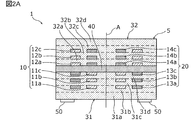
- FIG. 2A is a schematic cross-sectional view of the coil built-in component according to Embodiment 1.
- FIG. 2B is a diagram of the coil built-in component according to Embodiment 1 when viewed from the stacking direction.
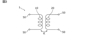
- FIG. 3 is an equivalent circuit of the coil built-in component according to the first embodiment.
- FIG. 4 is a schematic cross-sectional view of a coil built-in component according to Modification 1 of Embodiment 1.
- FIG. 5 is a schematic cross-sectional view of a coil built-in component according to Modification 2 of Embodiment 1.
- FIG. 6 is a schematic cross-sectional view of a coil built-in component according to the second embodiment.
- FIG. 1 is a perspective view of a coil built-in component according to Embodiment 1.
- FIG. 2A is a schematic cross-sectional view of the coil built-in component according to Embodiment
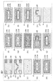
- FIG. 7 is a diagram showing each component (magnetic layer, intermediate layer, coil pattern, routing conductor pattern, external terminal) of the coil built-in component shown in FIG. 6, and (a) to (o) show each layer. It is the figure seen from the lower surface side.
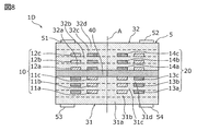
- FIG. 8 is a schematic diagram of a cross section of the coil built-in component according to the third embodiment.
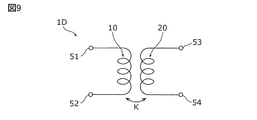
- FIG. 9 is an equivalent circuit of the coil built-in component according to the third embodiment.
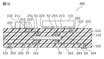
- FIG. 10 is a cross-sectional view of a resin multilayer substrate that includes the coil built-in component according to the third embodiment.
- the coil built-in component according to the present embodiment is a laminated coil built-in component including two coil elements.
- the coil built-in components are not limited to dual inductors such as common mode choke coils, transformers, couplers, and baluns, but may be built into multilayer circuit components such as multi-phase DC-DC converter choke coils. Good.
- a dual inductor will be described as an example of a coil built-in component.
- FIG. 1 is a perspective view of a coil built-in component 1 according to the present embodiment.
- 2A is a sectional view taken along the line IIA-IIA of the coil built-in component 1 shown in FIG. 1
- FIG. 2B is a diagram of the laminated coil built-in component 1 viewed from the stacking direction.
- FIG. 3 is an equivalent circuit of the coil built-in component 1.
- the coil built-in component 1 includes a multilayer body 5 and a plurality of external terminals 50 provided on the bottom surface of the multilayer body 5 as shown in FIG.
- a first coil element 10 and a second coil element 20 are provided inside the multilayer body 5.
- the first coil element 10 includes a first coil pattern 11 (11a, 11b, 11c) and a second coil pattern 12 (12a, 12b, 12c) connected in series to each other.
- the second coil element 20 includes a third coil pattern 13 (13a, 13b, 13c) and a fourth coil pattern 14 (14a, 14b, 14c) connected in series with each other.
- the first coil pattern 11, the second coil pattern 12, the third coil pattern 13, and the fourth coil pattern 14 are wound in a rectangular shape around the coil axis A, respectively. That is, the first coil element 10 and the second coil element 20 have the same coil axis A and are configured to be coupled via a magnetic field (see FIG. 3).
- the coil built-in component 1 has interlayer conductors (via conductors) and routing conductor patterns that connect the coil patterns, but these are not shown in FIGS. 2A and 2B.
- the multilayer body 5 has a first base material layer 31 and a second base material layer 32, and an intermediate layer 40 provided between the first base material layer 31 and the second base material layer 32.
- the first substrate layer 31 is formed by laminating a plurality of magnetic layers 31a, 31b, 31c, 31d.
- the second base material layer 32 is formed by laminating a plurality of magnetic layers 32a, 32b, 32c, 32d.
- the second base material layer 32 is provided on one side (upward in the present embodiment) in the stacking direction with respect to the first base material layer 31 via the intermediate layer 40.
- magnetic ferrite ceramics are used as the material of the magnetic layers 31a to 31d and 32a to 32d. Specifically, ferrite containing iron oxide as a main component and containing at least one of zinc, nickel, and copper is used.
- the intermediate layer 40 is formed between the first coil pattern 11c and the fourth coil pattern 14a adjacent to each other in the stacking direction and between the second coil pattern 12a and the third coil pattern 13c. It is provided in the entire region perpendicular to the stacking direction.
- the intermediate layer 40 is in contact with the first coil pattern 11c and the third coil pattern 13c on the lower surface side, and is in contact with the second coil pattern 12a and the fourth coil pattern 14a on the upper surface side.
- the intermediate layer 40 is a layer having a lower magnetic permeability than the magnetic layers 31a to 31d and 32a to 32d.
- a material having a relative permeability lower than that of the magnetic layers 31a to 31d and 32a to 32d is used.
- insulating glass mainly composed of nonmagnetic ferrite ceramics, alumina, and glass is used. Ceramics are used.
- the intermediate layer 40 may be called a nonmagnetic layer.
- the first coil patterns 11a, 11b, and 11c that are part of the first coil element 10 are provided in the first base material layer 31 so as to be adjacent to each other in the stacking direction.
- the second coil patterns 12a, 12b, 12c, which are part of the first coil element 10 are provided in the second base material layer 32 adjacent to each other in the stacking direction.
- the third coil patterns 13a, 13b, and 13c, which are part of the second coil element 20, are provided in the first base material layer 31 adjacent to each other in the stacking direction.
- the fourth coil patterns 14a, 14b, and 14c, which are part of the second coil element 20, are provided in the second base material layer 32 adjacent to each other in the stacking direction.
- the first coil pattern 11 is provided inside the third coil pattern 13.
- the first coil patterns 11a, 11b, 11c and the third coil patterns 13a, 13b, 13c are adjacent to each other in the stacking direction and the vertical direction.
- the fourth coil pattern 14 is provided inside the second coil pattern 12.
- the second coil patterns 12a, 12b, 12c and the fourth coil patterns 14a, 14b, 14c are adjacent to each other in the stacking direction and the vertical direction.
- the coil diameters of the first coil pattern 11 and the fourth coil pattern 14 are the same.
- the coil diameters of the second coil pattern 12 and the third coil pattern 13 are the same.
- the same coil diameter means that the long side and the short side have the same length.
- the first coil pattern 11, the second coil pattern 12, the third coil pattern 13, and the fourth coil pattern 14 have the same width dimension and the same thickness dimension.
- the second coil pattern 12 As a material of the first coil pattern 11, the second coil pattern 12, the third coil pattern 13, and the fourth coil pattern 14, for example, a metal or alloy mainly containing silver is used. Each of these coil patterns may be plated with, for example, nickel, palladium, or gold.
- the first coil pattern 11 and the fourth coil pattern 14 are overlapped, and the second coil pattern 12 and the second coil pattern 12 The three-coil pattern 13 overlaps.
- the winding axes of the first coil pattern 11 and the fourth coil pattern 14 and the winding axes of the second coil pattern 12 and the third coil pattern 13 are both on the same straight line (on the coil axis A).
- Interlinkage magnetic flux and interlinkage magnetic flux straddling the second coil pattern 12 and the third coil pattern 13 are formed. That is, in the coil built-in component 1, the first coil pattern 11 and the fourth coil pattern 14 disposed so as to sandwich the intermediate layer 40 are magnetically coupled, and the second coil pattern 12 disposed so as to sandwich the intermediate layer 40. And the third coil pattern 13 are magnetically coupled.
- a ceramic green sheet for a magnetic layer is prepared by sheet-forming a slurry containing magnetic ceramic powder, and an intermediate layer ceramic green is prepared by forming a slurry containing a non-magnetic ceramic powder.
- a ceramic green sheet for a magnetic layer is prepared by sheet-forming a slurry containing magnetic ceramic powder
- an intermediate layer ceramic green is prepared by forming a slurry containing a non-magnetic ceramic powder.
- a plurality of through holes are formed, and a conductor paste is filled in the through holes to form a plurality of via conductors, and the conductor paste is printed on the main surface to form the first coil
- the pattern 11 and the third coil pattern 13 or the second coil pattern 12 and the fourth coil pattern 14 are formed.
- the through hole is formed by, for example, laser processing.
- the first coil pattern 11, the second coil pattern 12, the third coil pattern, and the fourth coil pattern 14 are patterned by, for example, screen printing of a conductor paste containing Ag powder.
- Magnetic ceramics and non-magnetic ceramics are so-called LTCC ceramics (Low Temperature Co-fired Ceramics), whose firing temperature is below the melting point of silver, and silver is used as the material for each coil pattern and via conductor. It becomes possible.
- LTCC ceramics Low Temperature Co-fired Ceramics
- silver is used as the material for each coil pattern and via conductor. It becomes possible.
- the intermediate layer 40 can be easily formed in the entire region perpendicular to the stacking direction of the multilayer body 5 by using the sheet lamination method for producing the multilayer body 5 by laminating the ceramic green sheets as described above. be able to.
- the first coil pattern 11 of the first coil element 10 and the fourth coil pattern 14 of the second coil element 20 are seen from the stacking direction.
- the second coil pattern 12 of the first coil element 10 and the third coil pattern 13 of the second coil element 20 are overlapped.
- the first coil pattern 11 and the fourth coil pattern 14 are magnetically coupled via the intermediate layer 40
- the second coil pattern 12 and the third coil pattern 13 are magnetically coupled via the intermediate layer 40.
- the number of places where the first coil element 10 and the second coil element 20 are magnetically coupled can be increased.
- the number of magnetic field coupling is one.
- the first coil pattern 11 and the fourth coil pattern 14 and the second coil pattern 12 and the third coil pattern 13 are magnetically coupled at two locations. As a result, the number of magnetic field coupling points increases, and the magnetic coupling between the first coil element 10 and the second coil element 20 can be enhanced.
- the first coil pattern 11 and the fourth coil pattern 14 do not need to be completely overlapped, and at least part of them may be overlapped.
- the 2nd coil pattern 12 and the 3rd coil pattern 13 do not need to overlap completely, What is necessary is just to overlap at least one part.
- the first coil pattern 11 is provided inside the third coil pattern 13, and the fourth coil pattern 14 is provided inside the second coil pattern 12.
- coil patterns adjacent to each other in the direction perpendicular to the stacking direction are also coupled, so that the number of magnetic field coupling points increases.
- the first coil patterns 11a and 11b and the third coil patterns 13a and 13b are magnetically coupled to each other, and the second coil patterns 12b and 12c and the fourth coil patterns 14b and 14c are respectively coupled.
- the magnetic coupling between the first coil element 10 and the second coil element 20 can be further enhanced.
- the first coil element 10 and the second coil element 20 are opposite to each other in the stacking direction, and have a structure in which they enter each other.
- middle layer 40 and the 1st coil pattern 11a located in the outermost layer side can be shortened.
- the distance between the intermediate layer 40 and the second coil pattern 12c, the third coil pattern 13a, and the fourth coil pattern 14c located on the outermost layer side can be reduced.
- the magnetic coupling between the first coil element 10 and the second coil element 20 can be enhanced.
- the coil built-in component 1 in which the first coil element and the second coil element are arranged separately in the vertical direction as in the prior art, the distance between the coil pattern located on the outermost layer side and the intermediate layer becomes large. Therefore, a magnetic flux (minor loop) that circulates around the line of the coil pattern on the outermost layer side is generated, and there is a limit to increasing the magnetic coupling.
- the coil built-in component 1 according to the present embodiment has a structure in which the first coil element 10 and the second coil element 20 are inserted into each other. Therefore, when the number of coil turns is the same as that of the conventional technique, The distance from the first coil pattern 11a located on the outermost layer side is reduced.
- FIG. 4 is a schematic cross-sectional view of the coil built-in component 1A according to the first modification of the first embodiment.
- the widths of the coil patterns adjacent to each other in the stacking direction are different.
- the width of the first coil patterns 11a and 11c is larger than the width of the first coil pattern 11b, and the width of the second coil patterns 12a and 12c is larger than the width of the second coil pattern 12b.
- the width of the third coil patterns 13a and 13c is smaller than the width of the third coil pattern 13b, and the width of the fourth coil patterns 14a and 14c is smaller than the width of the fourth coil pattern 14b.
- the coil built-in component 1 ⁇ / b> A in the first modification when viewed from the stacking direction, the first coil pattern 11 and the fourth coil pattern 14 partially overlap each other, and one of the second coil pattern 12 and the third coil pattern 13. The parts overlap. According to this structure, in the coil built-in component 1 ⁇ / b> A, the number of magnetic field coupling portions between the first coil element 10 and the second coil element 20 can be increased, and magnetic coupling can be enhanced.
- this coil built-in component 1A since the width of the coil pattern adjacent in the laminating direction is changed, even when a positional deviation occurs in a direction perpendicular to the laminating direction when forming the coil pattern, The overlapping areas of the coil patterns when viewed from the direction are substantially the same. Thereby, the variation in the capacitive coupling generated by the two opposing coil patterns is suppressed, and the manufacturing variation in the inductance value and the magnetic coupling degree of the coil built-in component 1A can be suppressed.
- FIG. 5 is a schematic diagram of a cross section of the coil built-in component 1B according to the second modification of the first embodiment.
- the intermediate layer 40 is provided not in the entire region perpendicular to the stacking direction of the multilayer body 5 but in a part of the region.
- the intermediate layer 40 is between the first coil pattern 11c and the fourth coil pattern 14a adjacent in the stacking direction, between the second coil pattern 12a and the third coil pattern 13c adjacent in the stacking direction, In addition, it is provided only between the magnetic layer between the first coil pattern 11 and the third coil pattern 13 and the magnetic layer between the second coil pattern 12 and the fourth coil pattern 14. . That is, when viewed from the stacking direction, the intermediate layer 40 is not formed between the magnetic layer 31d inside the first coil pattern 11c and the magnetic layer 32a inside the fourth coil pattern 14a.
- the third base material layer 33 made of the same material as the magnetic layers 31a to 31d and 32a to 32d is formed. Further, when viewed from the stacking direction, the intermediate layer 40 is not formed on the outside of the third coil pattern 13 and the outside of the second coil pattern 12, and the third base material layer 33 is formed.
- the first coil pattern 11 and the fourth coil pattern 14 partially overlap, and the second coil pattern 12 and the third coil pattern 13 Part of is overlapping.
- the number of magnetic field coupling portions between the first coil element 10 and the second coil element 20 can be increased, and magnetic coupling can be enhanced.
- the magnetic flux is formed along the coil axis A inside the first coil pattern 11 and inside the fourth coil pattern 14, and the first coil element 10 and the second coil element 20 are included. Are not disturbed by the intermediate layer 40. Thereby, the magnetic coupling of the first coil element 10 and the second coil element 20 can be further enhanced.
- FIG. 6 is a schematic cross-sectional view of the coil built-in component 1C according to the second embodiment.
- FIG. 7 shows magnetic layers a to g and j to o, intermediate layers h and i forming the coil built-in component 1C, the first coil pattern 11, the second coil pattern 12, the third coil pattern 13, and the fourth coil pattern. 14 and routing conductor patterns p1 to p8.
- the coil built-in component 1 ⁇ / b> C includes a multilayer body 5 and a plurality of external terminals 50 provided on the bottom surface of the multilayer body 5.
- the first coil element 10 and the second coil element 20 are provided inside the multilayer body 5.
- the first coil element 10 includes a first coil pattern 11 (11a, 11b, 11c, 11d, 11e) and a second coil pattern 12 (12a, 12b, 12c, 12d) connected in series to each other.
- the second coil element 20 includes a third coil pattern 13 (13a, 13b, 13c, 13d, 13e) and a fourth coil pattern 14 (14a, 14b, 14c, 14d) connected in series to each other.
- the first coil pattern 11, the second coil pattern 12, the third coil pattern 13, and the fourth coil pattern 14 are wound around the coil axis A in a rectangular shape. That is, the first coil element 10 and the second coil element 20 have the same coil axis A and are configured to be coupled via a magnetic field.
- the multilayer body 5 includes a first base material layer 31 and a second base material layer 32, and intermediate layers h and i provided between the first base material layer 31 and the second base material layer 32. Yes.
- the first base material layer 31 is formed by laminating a plurality of magnetic layers a, b, c, d, e, f, and g.
- the second base material layer 32 is formed by laminating a plurality of magnetic layers j, k, l, m, and o.
- the second base material layer 32 is provided on one side (upward in the present embodiment) in the stacking direction with respect to the first base material layer 31 via the intermediate layers h and i.
- the intermediate layers h and i are laminated element bodies between the first coil pattern 11e and the fourth coil pattern 14a adjacent to each other in the lamination direction, and between the second coil pattern 12a and the third coil pattern 13e. 5 is provided in the entire region perpendicular to the stacking direction.
- the intermediate layers h and i are in contact with the first coil pattern 11e and the third coil pattern 13e, respectively, on the lower surface side, and are in contact with the second coil pattern 12a and the fourth coil pattern 14a, respectively, on the upper surface side. Yes.
- the first coil patterns 11a to 11e which are part of the first coil element 10 are provided in the first base material layer 31 adjacent to each other in the stacking direction.
- the second coil patterns 12a to 12d, which are part of the first coil element 10 are provided in the second base material layer 32 adjacent to each other in the stacking direction.
- the third coil patterns 13a to 13e, which are part of the second coil element 20, are provided in the first base material layer 31 adjacent to each other in the stacking direction.
- the fourth coil patterns 14a to 14d, which are part of the second coil element 20, are provided in the second base material layer 32 adjacent to each other in the stacking direction.
- the first coil pattern 11 is provided inside the third coil pattern 13.
- the first coil patterns 11a to 11e and the third coil patterns 13a to 13e are adjacent to each other in the stacking direction and the vertical direction.
- the fourth coil pattern 14 is provided inside the second coil pattern 12.
- the second coil patterns 12a to 12d and the fourth coil patterns 14a to 14d are adjacent to each other in the stacking direction and the vertical direction.
- the coil diameters of the first coil pattern 11 and the fourth coil pattern 14 are the same.
- the coil diameters of the second coil pattern 12 and the third coil pattern 13 are the same.
- the first coil pattern 11, the second coil pattern 12, the third coil pattern 13, and the fourth coil pattern 14 have the same width dimension and the same thickness dimension.
- the first coil pattern 11 and the fourth coil pattern 14 overlap, and the second coil pattern 12 and the third coil pattern 13 overlap. Yes.
- the winding axes of the first coil pattern 11 and the fourth coil pattern 14 and the winding axes of the second coil pattern 12 and the third coil pattern 13 are both on the same straight line (on the coil axis A).
- the first coil pattern 11 and the fourth coil pattern 14 arranged so as to sandwich the intermediate layers h and i are magnetically coupled, and the first coil pattern 11 and the fourth coil pattern 14 are arranged so as to sandwich the intermediate layers h and i.
- the two-coil pattern 12 and the third coil pattern 13 are configured to be magnetically coupled.
- each component (magnetic layer, intermediate layer, coil pattern, routing conductor pattern, external terminal) of the coil built-in component 1C will be described with reference to FIG. 7A to 7O show magnetic layers a to g, j to o, intermediate layers h and i, a first coil pattern 11, a second coil pattern 12, a third coil pattern 13, and a fourth coil. It is the figure which looked at the pattern 14 and the routing conductor patterns p1-p8 from the lower surface side.
- the layers a to o are stacked, they are stacked in the order of (a) to (o) with the bottom surfaces of the layers a to o facing downward.
- via conductor is indicated by a round shape in FIGS.
- Via conductors connect external terminals, routing conductor patterns, and coil patterns as shown in FIG.
- 7A is the outermost layer on the lower side of the multilayer body 5.
- Four external terminals 50 having a rectangular shape are formed on the bottom surface side of the magnetic layer a.
- lead conductor patterns p1, p2, p3, and p4 are formed.
- a first coil pattern 11a and a third coil pattern 13a are formed on the magnetic layer d shown in FIG.
- first coil pattern 11b and the third coil pattern 13b are formed in the magnetic layer e.
- a first coil pattern 11c and a third coil pattern 13c are formed on the magnetic layer f.
- a first coil pattern 11d and a third coil pattern 13d are formed on the magnetic layer g.
- a first coil pattern 11e and a third coil pattern 13e are formed in the intermediate layer h shown in (h) of FIG.
- the number of turns of the first coil pattern 11 and the third coil pattern 13 formed in each of the magnetic layers d to g and the intermediate layer h is 1 turn or less. Note that the number of turns of the first coil pattern 11 and the third coil pattern 13 may be 1/2 turn or more and less than 1 turn, 3/4 turn or more and less than 1 turn, It may be 8 turns or more and less than 1 turn, or 15/16 turns or more and less than 1 turn.
- routing conductor patterns p5 and p6 are formed.
- the second coil pattern 12a and the fourth coil pattern 14a are formed on the magnetic layer j shown in (j) of FIG.
- the second coil pattern 12b and the fourth coil pattern 14b are formed in the magnetic layer k.
- a second coil pattern 12c and a fourth coil pattern 14c are formed on the magnetic layer l.
- a second coil pattern 12d and a fourth coil pattern 14d are formed on the magnetic layer m.
- the number of turns of the second coil pattern 12 and the fourth coil pattern 14 formed in each of the magnetic layers j to m is 1 turn or less.
- the number of turns of the second coil pattern 12 and the fourth coil pattern 14 may be 1 ⁇ 2 turn or more and less than 1 turn, 3/4 turn or more and less than 1 turn, It may be 8 turns or more and less than 1 turn, or 15/16 turns or more and less than 1 turn.
- lead conductor patterns p7 and p8 are formed.
- the magnetic layer o shown in FIG. 7 (o) is the outermost layer on the upper side of the multilayer body 5.
- the magnetic layer o shown in FIG. 1 is the outermost layer on the upper side of the multilayer body 5.
- these magnetic layers a to g, intermediate layers h and i, and magnetic layers j to o are sequentially laminated, pressed, degreased and fired to produce the coil built-in component 1C.
- the same effect as that of the coil built-in component 1 shown in the first embodiment can be obtained. That is, the degree of coupling between the first coil element 10 and the second coil element 20 can be increased.
- the coupling coefficient K of both coil elements is about 0.7, but in the coil built-in component of the present embodiment, the coupling coefficient K of both coil elements is 0.8 or more. can do.
- FIG. 8 is a schematic view of a cross section of the coil built-in component 1D.
- FIG. 9 is an equivalent circuit of the coil built-in component 1D.
- the external terminals 53 and 54 are provided on the bottom surface of the multilayer body 5, and the external terminals 51 and 52 are provided on the top surface opposite to the bottom surface.
- An external terminal 51 is connected to one end of the first coil element 10, and an external terminal 52 is connected to the other end.
- An external terminal 53 is connected to one end of the second coil element 20, and an external terminal 54 is connected to the other end.
- the coil built-in component 1D when viewed from the stacking direction, a part of the first coil pattern 11 and the fourth coil pattern 14 overlap, and a part of the second coil pattern 12 and the third coil pattern 13 overlap. Yes.
- the number of magnetic field coupling portions between the first coil element 10 and the second coil element 20 can be increased, and magnetic coupling can be enhanced.
- FIG. 10 is a cross-sectional view of a resin multilayer substrate 310 having a coil built-in component 1D therein.
- the resin multilayer substrate 310 includes a resin multilayer substrate 310 and mounting components 131 and 132 mounted on the resin multilayer substrate 310.
- the coil built-in component 1D is a transformer component between the external circuit and the mounting components 131 and 132. Function as.
- the resin multilayer substrate 310 is a circuit board on which various electronic components are mounted and provided with a wiring pattern for connecting them.
- it is a substrate formed by laminating and pressing a plurality of resin base material layers 112.
- a thermoplastic resin sheet such as a liquid crystal polymer (LCP) or polyimide is used.
- the resin multilayer substrate 310 includes in-plane conductors 211, 213, 241, 243, interlayer conductors 251, 255, 261, 265, 321, 322, 331, 332, top surface conductors 221, 222, 225, and 226. A conductor is provided. External circuit connection terminals 353 and 354 are provided on the bottom surface of the resin multilayer substrate 310.
- the coil built-in component 1D is entirely embedded in the resin multilayer substrate 310.
- the external terminal 51 of the coil built-in component 1D is connected to the mounting component 132 via the interlayer conductor 251, the in-plane conductor 211, the interlayer conductor 321, and the top conductor 222.
- the external terminal 52 includes the interlayer conductor 255, The in-plane conductor 213, the interlayer conductor 322, and the top surface conductor 226 are connected to the mounting component 131.
- the external terminal 53 is connected to the external circuit connection terminal 353 via the interlayer conductor 261, the in-plane conductor 241, and the interlayer conductor 331.
- the external terminal 54 is connected to the external circuit connection terminal 354 via the interlayer conductor 265, the in-plane conductor 243, and the interlayer conductor 332.
- circuit module 300 having the coil built-in component 1D having high magnetic coupling.
- each of the first base material layer and the second base material layer is configured by a plurality of magnetic layers.
- each base material layer is a single magnetic layer. It may be constituted by.
- the intermediate layer may be composed of one layer or may be composed of a plurality of layers.
- the laminated element body has a two-stage structure, but is not limited thereto, and may have a three-stage structure or more.
- a first base material layer, an intermediate layer, a second base material layer, an intermediate layer, and an uppermost base material layer are sequentially laminated, and connected to the third coil pattern in the uppermost base material layer.
- a fifth coil pattern may be formed, and a sixth coil pattern connected to the fourth coil pattern may be formed.
- the equivalent circuit shown in FIG. 3 four terminals are shown as external terminals, but two terminals on the output side may be connected to one terminal by using a coil built-in component.
- the stacking direction of the coil built-in components may be upside down.
- the coil pattern of the coil built-in component may be one, half or spiral.
- the intermediate layer may be provided so that the magnetic layer and the intermediate layer are symmetrical in the stacking direction.
- the coil built-in component of the present invention can be widely used in the form of being built in a multilayer circuit component such as a dual inductor such as a common mode choke coil, transformer, coupler, and balun, or a choke coil of a multi-phase DC-DC converter. it can.
- a multilayer circuit component such as a dual inductor such as a common mode choke coil, transformer, coupler, and balun, or a choke coil of a multi-phase DC-DC converter. it can.
Landscapes
- Engineering & Computer Science (AREA)
- Power Engineering (AREA)
- Coils Or Transformers For Communication (AREA)
- Coils Of Transformers For General Uses (AREA)
Abstract
第1コイル素子(10)は、第1コイルパターン(11)と第2コイルパターン(12)とを含み、第2コイル素子(20)は、第3コイルパターン(13)と第4コイルパターン(14)とを含んでいる。第1コイルパターン(11)および第3コイルパターン(13)は第1基材層(31)に設けられ、第2コイルパターン(12)および第4コイルパターン(14)は第2基材層(32)に設けられている。コイル内蔵部品(1)を積層方向から見た場合、第1コイルパターン(11)と第4コイルパターン(14)は少なくとも一部が重なっており、第2コイルパターン(12)と第3コイルパターン(13)は少なくとも一部が重なっている。第1コイルパターン(11)と第4コイルパターン(14)との間、および、第2コイルパターン(12)と第3コイルパターン(13)との間には、透磁率の低い中間層(40)が設けられている。
Description
本発明は、コイル内蔵部品に関し、特には、2つのコイル素子を内蔵する積層型のコイル内蔵部品に関する。
従来、多層基板内に2つのコイル素子が形成されたコイル内蔵部品が知られている(例えば、特許文献1参照)。
特許文献1に示されたコイル内蔵部品は、複数の磁性体層が積層された積層素体と、積層素体内に設けられた第1コイル素子と第2コイル素子とを有している。第1コイル素子と第2コイル素子とは、積層方向の上下に分かれて配置され、磁界を介して結合するように構成されている。積層方向に隣り合う第1コイル素子のコイルパターンと第2コイル素子のコイルパターンとの間には、非磁性体部が設けられている。
一般に、2つのコイル素子を内蔵するコイル内蔵部品のインダクタンス値や磁界的な結合を高めるためには、コイル内蔵部品の積層数を増やし、コイルの巻数を増やすことが行われる。しかし、単純に積層数を増やした場合、インダクタンス値を大きくすることはできるが、2つのコイル素子の磁界的な結合を高めることはできなかった。すなわち、特許文献1に示すコイル内蔵部品のように、第1コイル素子と第2コイル素子とを上下に分けて配置した構造では、2つのコイル素子の磁界的な結合を高めることが困難であった。
そこで、本発明は、2つのコイル素子の磁界的な結合を高めることができるコイル内蔵部品を提供することを目的とする。
上記目的を達成するために、本発明の一態様に係るコイル内蔵部品は、複数の磁性体層を積層してなる積層素体と、前記積層素体内に設けられた第1コイル素子および第2コイル素子とを備えるコイル内蔵部品であって、前記積層素体は、1以上の前記磁性体層を有する第1基材層と、1以上の前記磁性体層を有し、前記第1基材層に対して積層方向に設けられた第2基材層とを含み、前記第1コイル素子は、互いに接続された第1コイルパターンと第2コイルパターンとを含み、前記第2コイル素子は、互いに接続された第3コイルパターンと第4コイルパターンとを含み、前記第1コイルパターンおよび前記第3コイルパターンは前記第1基材層に設けられ、前記第2コイルパターンおよび前記第4コイルパターンは前記第2基材層に設けられ、前記積層方向から見た場合、前記第1コイルパターンと前記第4コイルパターンとは少なくとも一部が重なっており、前記第2コイルパターンと前記第3コイルパターンとは少なくとも一部が重なっており、前記第1コイルパターンと前記第4コイルパターンとの間、および、前記第2コイルパターンと前記第3コイルパターンとの間には、前記磁性体層よりも透磁率の低い中間層が設けられている。
これによれば、中間層を介して第1コイルパターンと第4コイルパターンとが磁界結合し、中間層を介して第2コイルパターンと第3コイルパターンとが磁界結合する。よって、第1コイル素子と第2コイル素子との磁界結合する箇所が増えるので、第1コイル素子と第2コイル素子との磁界的な結合を高めることができる。
また、前記コイル内蔵部品を前記積層方向から見た場合、前記第1コイルパターンは前記第3コイルパターンの内側に設けられ、前記第4コイルパターンは前記第2コイルパターンの内側に設けられていてもよい。
これによれば、第1コイルパターンと第3コイルパターンとの磁界結合、および、第2コイルパターンと第4コイルパターンとの磁界結合を得ることができる。これにより、第1コイル素子と第2コイル素子との磁界的な結合を高めることができる。
また、前記第1コイル素子のコイル軸と前記第2コイル素子のコイル軸とが一致していてもよい。
これによれば、コイルパターン内に形成される磁界を高効率に結合できるので、第1コイル素子により形成される磁界と第2コイル素子により形成される磁界との結合をより高めることができる。
また、前記第1コイルパターンと前記第4コイルパターンとのコイル径が同じであり、前記第2コイルパターンと前記第3コイルパターンとのコイル径が同じであってもよい。
これによれば、第1コイルパターンにより形成される磁界と第4コイルパターンにより形成される磁界との結合をより高めることができる。また、第2コイルパターンにより形成される磁界と第3コイルパターンにより形成される磁界との結合をより高めることができる。
また、前記第1コイルパターンおよび前記第3コイルパターンが形成される前記磁性体層は、その1層につき、前記第1コイルパターンと前記第3コイルパターンとをそれぞれ1ターン以下備え、前記第2コイルパターンおよび前記第4コイルパターンが形成される前記磁性体層は、その1層につき、前記第2コイルパターンと前記第4コイルパターンとをそれぞれ1ターン以下備えていてもよい。
これによれば、磁性体層の1層が1ターンより多い巻き数を有するコイルパターンを備える場合に比べて、積層方向に対向するコイルパターンの容量的な結合を減らすことができる。その結果、コイル内蔵部品のインダクタンス値の低下を抑制することができる。
また、前記第1基材層は、前記積層方向に互いに隣り合う複数の前記第1コイルパターンと、前記積層方向に互いに隣り合う数の前記第3コイルパターンとを有し、前記第2基材層は、前記積層方向に互いに隣り合う複数の前記第2コイルパターンと、前記積層方向に互いに隣り合う複数の前記第4コイルパターンとを有していてもよい。
これによれば、第1コイル素子および第2コイル素子のそれぞれのインダクタンス値を大きくするとともに、第1コイル素子と第2コイル素子との磁界的な結合を高めることができる。
また、前記中間層は、前記積層方向に隣り合う前記第1コイルパターンと前記第4コイルパターンとの間、および、前記積層方向に隣り合う前記第2コイルパターンと前記第3コイルパターンとの間にて、前記積層素体の前記積層方向に垂直な全領域に設けられていてもよい。
これによれば、積層素体内に、透磁率の低い中間層を容易に形成することができる。
また、前記中間層は、前記第1コイルパターンの内側にある前記磁性体層と前記第4コイルパターンの内側にある前記磁性体層の間には設けられておらず、前記積層方向に隣り合う前記第1コイルパターンと前記第4コイルパターンとの間、前記積層方向に隣り合う前記第2コイルパターンと前記第3コイルパターンとの間、および、前記第1コイルパターンと前記第3コイルパターンとの間にある前記磁性体層と前記第2コイルパターンと前記第4コイルパターンとの間にある前記磁性体層との間に設けられていてもよい。
これによれば、第1コイルパターンの内側および第4コイルパターンの内側においてコイル軸に沿って形成される磁束が中間層によって妨げられることがなくなり、第1コイル素子と第2コイル素子の磁界的な結合をさらに高めることができる。
本発明によれば、コイル内蔵部品に内蔵されている2つのコイル素子の磁界的な結合を高めることができる。
以下、本発明の実施の形態について、図面を用いて詳細に説明する。なお、以下で説明する実施の形態は、いずれも包括的または具体的な例を示すものである。以下の実施の形態で示される数値、形状、材料、構成要素、構成要素の配置および接続形態、製造工程、および製造工程の順序などは、一例であり、本発明を限定する主旨ではない。以下の実施の形態における構成要素のうち、独立請求項に記載されていない構成要素については、任意の構成要素として説明される。
なお、各図は、模式図であり、必ずしも厳密に図示されたものではない。また、各図において、実質的に同一の構成に対しては同一の符号を付しており、重複する説明は省略または簡略化する。
(実施の形態1)
本実施の形態に係るコイル内蔵部品は、2つのコイル素子を内蔵する積層型のコイル内蔵部品である。このコイル内蔵部品は、コモンモードチョークコイル、トランス、カプラ、バランなどのようなデュアルインダクタに限られず、マルチフェーズ用DC-DCコンバータのチョークコイルなどの多層回路部品に内蔵される形態であってもよい。本実施の形態では、コイル内蔵部品として、デュアルインダクタを例に挙げて説明する。
本実施の形態に係るコイル内蔵部品は、2つのコイル素子を内蔵する積層型のコイル内蔵部品である。このコイル内蔵部品は、コモンモードチョークコイル、トランス、カプラ、バランなどのようなデュアルインダクタに限られず、マルチフェーズ用DC-DCコンバータのチョークコイルなどの多層回路部品に内蔵される形態であってもよい。本実施の形態では、コイル内蔵部品として、デュアルインダクタを例に挙げて説明する。
図1は本実施の形態に係るコイル内蔵部品1の斜視図である。図2Aは、図1に示すコイル内蔵部品1のIIA-IIA断面式図であり、図2Bは、積層型のコイル内蔵部品1を積層方向から見た場合の図である。図3は、コイル内蔵部品1の等価回路である。
コイル内蔵部品1は、図1に示されるように、積層素体5と、積層素体5の底面に設けられた複数の外部端子50とを備えている。
積層素体5の内部には、図2Aに示されるように、第1コイル素子10および第2コイル素子20が設けられている。第1コイル素子10は、互いに直列接続された第1コイルパターン11(11a、11b、11c)と第2コイルパターン12(12a、12b、12c)とを含んでいる。第2コイル素子20は、互いに直列接続された第3コイルパターン13(13a、13b、13c)と、第4コイルパターン14(14a、14b、14c)とを含んでいる。第1コイルパターン11、第2コイルパターン12、第3コイルパターン13および第4コイルパターン14は、図2Bに示されるように、コイル軸Aを中心に、矩形状にそれぞれ巻回されている。すなわち、第1コイル素子10と第2コイル素子20とは、コイル軸Aが一致しており、磁界を介して結合するように構成されている(図3参照)。
なお、コイル内蔵部品1は、各コイルパターンを接続する層間導体(ビア導体)や引き回し導体パターンを有しているが、図2Aおよび図2Bでは、それらの図示を省略している。
積層素体5は、第1基材層31および第2基材層32と、第1基材層31と第2基材層32との間に設けられる中間層40とを有している。
第1基材層31は、複数の磁性体層31a、31b、31c、31dが積層されることにより形成されている。第2基材層32は、複数の磁性体層32a、32b、32c、32dが積層されることにより形成されている。第2基材層32は、中間層40を介して、第1基材層31に対して積層方向の一方側(本実施の形態では上方)に設けられている。
磁性体層31a~31d、32a~32dの材料としては、例えば、磁性フェライトセラミックスが用いられる。具体的には、酸化鉄を主成分とし、亜鉛、ニッケル及び銅のうち少なくとも1つ以上を含むフェライトが用いられる。
中間層40は、積層方向に隣り合う第1コイルパターン11cと、第4コイルパターン14aとの間、および、第2コイルパターン12aと第3コイルパターン13cとの間にて、積層素体5の積層方向に垂直な全領域に設けられている。また、中間層40は、その下面側において第1コイルパターン11cおよび第3コイルパターン13cにそれぞれ接触しており、上面側において第2コイルパターン12aおよび第4コイルパターン14aにそれぞれ接触している。
中間層40は、磁性体層31a~31d、32a~32dよりも透磁率の低い層である。中間層40の材料としては、磁性体層31a~31d、32a~32dの材料よりも比透磁率の低い材料が用いられ、例えば、非磁性フェライトセラミックスやアルミナおよびガラスを主成分とする絶縁性ガラスセラミックスが用いられる。なお、この中間層40は、非磁性体層と呼ばれることもある。
第1コイル素子10の一部である第1コイルパターン11a、11b、11cは、積層方向に互いに隣り合って第1基材層31内に設けられている。第1コイル素子10の一部である第2コイルパターン12a、12b、12cは、積層方向に互いに隣り合って第2基材層32内に設けられている。第2コイル素子20の一部である第3コイルパターン13a、13b、13cは積層方向に互いに隣り合って第1基材層31内に設けられている。第2コイル素子20の一部である第4コイルパターン14a、14b、14cは積層方向に互いに隣り合って第2基材層32内に設けられている。
また、第1コイルパターン11は、第3コイルパターン13の内側に設けられている。第1コイルパターン11a、11b、11cおよび第3コイルパターン13a、13b、13cは、積層方向と垂直方向にそれぞれ互いに隣り合っている。第4コイルパターン14は、第2コイルパターン12の内側に設けられている。第2コイルパターン12a、12b、12cおよび第4コイルパターン14a、14b、14cは、積層方向と垂直方向にそれぞれ互いに隣り合っている。これにより、第1コイル素子10と第2コイル素子20は、積層方向において互いに逆向となって、互いに入り込んだ構造となっている。
また、第1コイルパターン11と第4コイルパターン14とのコイル径は同じでる。第2コイルパターン12と第3コイルパターン13とのコイル径は同じである。コイル径が同じとは、比較する2つのコイルパターンが矩形状である場合、長辺および短辺の長さがそれぞれ同じであることを意味する。なお、第1コイルパターン11、第2コイルパターン12、第3コイルパターン13および第4コイルパターン14の幅寸法はそれぞれ同じであり、厚み寸法もそれぞれ同じである。
第1コイルパターン11、第2コイルパターン12、第3コイルパターン13および第4コイルパターン14の材料としては、例えば、銀を主成分とする金属又は合金が用いられる。これらのコイルパターンそれぞれに、例えば、ニッケル、パラジウム、又は金によるめっきが施されていてもよい。
本実施の形態では、図2Bに示されるように、コイル内蔵部品1を積層方向から見た場合、第1コイルパターン11と第4コイルパターン14とが重なっており、第2コイルパターン12と第3コイルパターン13とが重なっている。そして、第1コイルパターン11と第4コイルパターン14の巻回軸、および、第2コイルパターン12と第3コイルパターン13の巻回軸が、ともに同じ直線上(コイル軸A上)にある。この構造により、第1コイル素子10および第2コイル素子20のそれぞれに電圧を印加した場合、コイル軸Aに沿った磁束であって、第1コイルパターン11と第4コイルパターン14とを跨って鎖交する磁束、および、第2コイルパターン12と第3コイルパターン13とを跨って鎖交する磁束が形成される。すなわち、コイル内蔵部品1では、中間層40を挟むように配置された第1コイルパターン11と第4コイルパターン14とが磁界結合し、中間層40を挟むように配置された第2コイルパターン12と第3コイルパターン13とが磁界結合するように構成されている。
次に、コイル内蔵部品1の製造工程について説明する。
まず、各層のセラミックグリーンシートを準備する。具体的には、磁性体セラミック粉末を含んだスラリーをシート成形することによって磁性体層用セラミックグリーンシートを準備し、非磁性体セラミック粉末を含んだスラリーをシート成形することによって中間層用セラミックグリーンシートを準備する。
次いで、所定のセラミックグリーンシートにおいて、複数の貫通孔を形成し、当該貫通孔内に導体ペーストを充填して複数のビア導体を形成するとともに、主面上に導体ペーストを印刷して第1コイルパターン11および第3コイルパターン13、または、第2コイルパターン12および第4コイルパターン14を形成する。貫通孔は、例えば、レーザー加工により形成される。第1コイルパターン11、第2コイルパターン12、第3コイルパターンおよび第4コイルパターン14は、例えば、Ag粉末を含んだ導体ペーストのスクリーン印刷によりパターニングされる。
次いで、導体ペーストが配置された複数のセラミックグリーンシートを積層・圧着した後、カットして個片化し、その後、一括して焼成する。この焼成により、各グリーンシート中の磁性体セラミック粉末、非磁性体セラミック粉末が焼結するとともに、導体ペースト中のAg粉末が焼結する。
磁性体セラミックスおよび非磁性体セラミックスは、いわゆるLTCCセラミックス(Low Temperature Co-fired Ceramics)であり、その焼成温度が銀の融点以下であって、各コイルパターンやビア導体の材料として銀を用いることが可能になる。抵抗率の低い銀を用いて第1コイル素子10および第2コイル素子20を構成することで、損失が少ないコイル内蔵部品1を作製することができる。
また、上記のようにセラミックグリーンシートを積層して積層素体5を作製するシート積層工法を用いることで、中間層40を、積層素体5の積層方向に垂直な全領域に容易に形成することができる。
以上説明したように、本実施の形態に係るコイル内蔵部品1では、積層方向から見た場合、第1コイル素子10の第1コイルパターン11と第2コイル素子20の第4コイルパターン14とが重なっており、かつ、第1コイル素子10の第2コイルパターン12と第2コイル素子20の第3コイルパターン13とが重なっている。この構造によれば、中間層40を介して第1コイルパターン11と第4コイルパターン14とが磁界結合し、中間層40を介して第2コイルパターン12と第3コイルパターン13とが磁界結合する。その結果、第1コイル素子10と第2コイル素子20との磁界結合する箇所を増やすことができる。
例えば、従来技術に示されたコイル内蔵部品では、対向する一対のコイル素子で磁界結合するので、磁界結合する箇所は1箇所である。それに対し、本実施の形態に係るコイル内蔵部品1では、第1コイルパターン11と第4コイルパターン14、および、第2コイルパターン12と第3コイルパターン13の2箇所で磁界結合する。これにより、磁界結合する箇所が増え、第1コイル素子10と第2コイル素子20との磁界的な結合を高めることができる。
なお、コイル内蔵部品1を積層方向から見た場合、第1コイルパターン11と第4コイルパターン14とが、完全に重なっている必要はなく、少なくとも一部が重なっていればよい。また、第2コイルパターン12と第3コイルパターン13とが、完全に重なっている必要はなく、少なくとも一部が重なっていればよい。
また、コイル内蔵部品1では、第1コイルパターン11が第3コイルパターン13の内側に設けられ、第4コイルパターン14が第2コイルパターン12の内側に設けられている。この構造により、積層方向と垂直な方向に隣り合うコイルパターン同士も結合するので、磁界結合する箇所が増える。具体的には、コイル内蔵部品1において、第1コイルパターン11a、11bと第3コイルパターン13a、13bとがそれぞれ磁界結合し、また、第2コイルパターン12b、12cと第4コイルパターン14b、14cとがそれぞれ磁界結合する。これにより、第1コイル素子10と第2コイル素子20との磁界的な結合をさらに高めることができる。
また、コイル内蔵部品1では、第1コイル素子10と第2コイル素子20とが、積層方向において互いに逆向となって、互いに入り込んだ構造となっている。これにより、中間層に対して複数のコイルパターンを単純に積み上げた構造に比べて、中間層40と最外層側に位置する第1コイルパターン11aとの距離を縮めることができる。同様に、中間層40と最外層側に位置する第2コイルパターン12c、第3コイルパターン13aおよび第4コイルパターン14cとの距離をそれぞれ縮めることができる。その結果、第1コイル素子10と第2コイル素子20との磁界的な結合を高めることができる。
例えば、従来技術のように第1コイル素子と第2コイル素子を上下に分けて配置したコイル内蔵部品では、最外層側に位置するコイルパターンと中間層との距離が大きくなる。そのため、最外層側のコイルパターンの線路の周囲を周回する磁束(マイナーループ)が発生し、磁界的な結合を高めることに限界がある。しかし、本実施の形態に係るコイル内蔵部品1では、第1コイル素子10と第2コイル素子20を互いに入り込んだ構造としているので、従来技術とコイル巻き数を同じにした場合、中間層40と最外層側に位置する第1コイルパターン11aとの距離が小さくなる。そのため、第1コイルパターン11aの線路の周囲を周回する磁束の発生を抑制することができる。同様に、中間層40と、最外層側に位置する第2コイルパターン12c、第3コイルパターン13aおよび第4コイルパターン14cとの距離がそれぞれ小さくなる。そのため、第2コイルパターン12c、第3コイルパターン13aおよび第4コイルパターン14cの線路の周囲を周回する磁束の発生をそれぞれ抑制することができる。その結果、第1コイル素子10と第2コイル素子との磁界的な結合を高めることができる。また、コイル内蔵部品1の厚みを小さくすることができる。
(実施の形態1の変形例)
次に、実施の形態1の変形例におけるコイル内蔵部品について説明する。
次に、実施の形態1の変形例におけるコイル内蔵部品について説明する。
図4は、実施の形態1の変形例1におけるコイル内蔵部品1Aの断面の模式図である。変形例1におけるコイル内蔵部品1Aでは、積層方向に隣り合うコイルパターンの幅が異なっている。
具体的には、第1コイルパターン11a、11cの幅が、第1コイルパターン11bの幅よりも大きく、第2コイルパターン12a、12cの幅が、第2コイルパターン12bの幅よりも大きくなっている。また、第3コイルパターン13a、13cの幅が、第3コイルパターン13bの幅よりも小さく、第4コイルパターン14a、14cの幅が、第4コイルパターン14bの幅よりも小さくなっている。
変形例1におけるコイル内蔵部品1Aにおいても、積層方向から見た場合、第1コイルパターン11と第4コイルパターン14の一部が重なっており、第2コイルパターン12と第3コイルパターン13の一部が重なっている。この構造によれば、コイル内蔵部品1Aにおいて、第1コイル素子10と第2コイル素子20との磁界結合する箇所を増やすことができ、磁界的な結合を高めることができる。
また、このコイル内蔵部品1Aでは、積層方向に隣り合うコイルパターンの幅を変えているので、コイルパターンを形成する際に積層方向と垂直な方向に位置ずれが生じた場合であっても、積層方向から見た場合のコイルパターン同士の重なり面積がほぼ同じになる。これにより、対向する2つのコイルパターンで発生する容量的な結合のばらつきが抑制され、コイル内蔵部品1Aのインダクタンス値および磁界的な結合度の製造ばらつきを抑えることができる。
図5は、実施の形態1の変形例2におけるコイル内蔵部品1Bの断面の模式図である。
変形例2におけるコイル内蔵部品1Bでは、中間層40が、積層素体5の積層方向に垂直な全領域に設けられているのでなく、一部の領域に設けられている。
具体的には、中間層40が、積層方向に隣り合う第1コイルパターン11cと第4コイルパターン14aとの間、積層方向に隣り合う第2コイルパターン12aと第3コイルパターン13cとの間、および、第1コイルパターン11と第3コイルパターン13との間にある磁性体層と第2コイルパターン12と第4コイルパターン14との間にある磁性体層との間のみに設けられている。すなわち、積層方向から見た場合、第1コイルパターン11cの内側にある磁性体層31dと第4コイルパターン14aの内側にある磁性体層32aとの間には、中間層40が形成されておらず、磁性体層31a~31d、32a~32dと同じ材料からなる第3基材層33が形成されている。また、積層方向から見た場合、第3コイルパターン13の外側および第2コイルパターン12の外側には、中間層40が形成されておらず、第3基材層33が形成されている。
変形例2におけるコイル内蔵部品1Bにおいても、積層方向から見た場合、第1コイルパターン11と第4コイルパターン14との一部が重なっており、第2コイルパターン12と第3コイルパターン13との一部が重なっている。この構造によれば、コイル内蔵部品1Bにおいて、第1コイル素子10と第2コイル素子20との磁界結合する箇所を増やすことができ、磁界的な結合を高めることができる。
また、このコイル内蔵部品1Bでは、第1コイルパターン11の内側および第4コイルパターン14の内側においてコイル軸Aに沿って形成される磁束であって、第1コイル素子10と第2コイル素子20とを鎖交する磁束(メジャーループ)が、中間層40によって妨げられることがなくなる。これにより、第1コイル素子10と第2コイル素子20の磁界的な結合をさらに高めることができる。
(実施の形態2)
次に、実施の形態2に係るコイル内蔵部品について説明する。
次に、実施の形態2に係るコイル内蔵部品について説明する。
図6は、実施の形態2に係るコイル内蔵部品1Cの断面の模式図である。図7は、コイル内蔵部品1Cを形成する磁性体層a~g、j~o、中間層h、i、第1コイルパターン11、第2コイルパターン12、第3コイルパターン13、第4コイルパターン14、および、引き回し導体パターンp1~p8を示す図である。
コイル内蔵部品1Cは、図6に示されるように、積層素体5と、積層素体5の底面に設けられた複数の外部端子50とを備えている。
積層素体5の内部には、第1コイル素子10および第2コイル素子20が設けられている。第1コイル素子10は、互いに直列接続された第1コイルパターン11(11a、11b、11c、11d、11e)と第2コイルパターン12(12a、12b、12c、12d)とを含んでいる。第2コイル素子20は、互いに直列接続された第3コイルパターン13(13a、13b、13c、13d、13e)と第4コイルパターン14(14a、14b、14c、14d)とを含んでいる。第1コイルパターン11、第2コイルパターン12、第3コイルパターン13および第4コイルパターン14は、コイル軸Aを中心に、矩形状にそれぞれ巻回されている。すなわち、第1コイル素子10と第2コイル素子20とは、コイル軸Aが一致しており、磁界を介して結合するように構成されている。
積層素体5は、第1基材層31および第2基材層32と、第1基材層31と第2基材層32との間に設けられる中間層h、iとを有している。
第1基材層31は、複数の磁性体層a、b、c、d、e、f、gが積層されることにより形成されている。第2基材層32は、複数の磁性体層j、k、l、m、oが積層されることにより形成されている。第2基材層32は、中間層h、iを介して、第1基材層31に対して積層方向の一方側(本実施の形態では上方)に設けられている。
中間層h、iは、積層方向に隣り合う第1コイルパターン11eと、第4コイルパターン14aとの間、および、第2コイルパターン12aと第3コイルパターン13eとの間にて、積層素体5の積層方向に垂直な全領域に設けられている。また、中間層h,iは、その下面側において第1コイルパターン11eおよび第3コイルパターン13eにそれぞれ接触しており、上面側において第2コイルパターン12aおよび第4コイルパターン14aにそれぞれ接触している。
第1コイル素子10の一部である第1コイルパターン11a~11eは、積層方向に互いに隣り合って第1基材層31内に設けられている。第1コイル素子10の一部である第2コイルパターン12a~12dは、積層方向に互いに隣り合って第2基材層32内に設けられている。第2コイル素子20の一部である第3コイルパターン13a~13eは積層方向に互いに隣り合って第1基材層31内に設けられている。第2コイル素子20の一部である第4コイルパターン14a~14dは積層方向に互いに隣り合って第2基材層32内に設けられている。
また、第1コイルパターン11は、第3コイルパターン13の内側に設けられている。第1コイルパターン11a~11eおよび第3コイルパターン13a~13eは、積層方向と垂直方向にそれぞれ互いに隣り合っている。第4コイルパターン14は、第2コイルパターン12の内側に設けられている。第2コイルパターン12a~12dおよび第4コイルパターン14a~14dは、積層方向と垂直方向にそれぞれ互いに隣り合っている。これにより、第1コイル素子10と第2コイル素子20は、積層方向において互いに逆向となって、互いに入り込んだ構造となっている。
また、第1コイルパターン11と第4コイルパターン14とのコイル径は同じである。第2コイルパターン12と第3コイルパターン13とのコイル径は同じである。なお、第1コイルパターン11、第2コイルパターン12、第3コイルパターン13および第4コイルパターン14の幅寸法はそれぞれ同じであり、厚み寸法もそれぞれ同じである。
本実施の形態では、コイル内蔵部品1Cを積層方向から見た場合、第1コイルパターン11と第4コイルパターン14とが重なっており、第2コイルパターン12と第3コイルパターン13とが重なっている。そして、第1コイルパターン11と第4コイルパターン14の巻回軸、および、第2コイルパターン12と第3コイルパターン13の巻回軸が、ともに同じ直線上(コイル軸A上)にある。この構造により、第1コイル素子10および第2コイル素子20のそれぞれに電圧を印加した場合、コイル軸Aに沿った磁束であって、第1コイルパターン11と第4コイルパターン14とを跨って鎖交する磁束、および、第2コイルパターン12と第3コイルパターン13とを跨って鎖交する磁束が形成される。すなわち、コイル内蔵部品1Cでは、中間層h、iを挟むように配置された第1コイルパターン11と第4コイルパターン14とが磁界結合し、中間層h、iを挟むように配置された第2コイルパターン12と第3コイルパターン13とが磁界結合するように構成されている。
次に、図7を参照しつつ、コイル内蔵部品1Cの各構成要素(磁性体層、中間層、コイルパターン、引き回し導体パターン、外部端子)について説明する。図7の(a)~(o)は、磁性体層a~g、j~o、中間層h,i、第1コイルパターン11、第2コイルパターン12、第3コイルパターン13、第4コイルパターン14、および、引き回し導体パターンp1~p8を下面側から見た図である。各層a~oが積層される際は、各層a~oの下面を下向きにした状態で、(a)~(o)の順に積み重ねられる。
なお、ビア導体は、図7の(a)~(m)において丸形状で示されている。ビア導体は外部端子、引き回し導体パターン、各コイルパターンを図7に示されるように繋いでいる。
図7の(a)に示す磁性体層aは、積層素体5の下側の最外層である。磁性体層aには、その底面側に矩形状の4つの外部端子50が形成されている。
図7の(b)に示す磁性体層bには、引き回し導体パターンp1、p2、p3、p4が形成されている。
図7の(c)に示す磁性体層cには、4つのビア導体が形成されている。
図7の(d)に示す磁性体層dには、第1コイルパターン11aと、第3コイルパターン13aが形成されている。
同様に、磁性体層eには、第1コイルパターン11bと第3コイルパターン13bとが形成されている。磁性体層fには、第1コイルパターン11cと第3コイルパターン13cとが形成されている。磁性体層gには、第1コイルパターン11dと第3コイルパターン13dとが形成されている。
図7の(h)に示す中間層hには、第1コイルパターン11eと第3コイルパターン13eが形成されている。
磁性体層d~g、中間層hのそれぞれに形成される第1コイルパターン11および第3コイルパターン13の巻き数は、それぞれ1ターン以下である。なお、第1コイルパターン11および第3コイルパターン13の巻き数は、1/2ターン以上1ターン未満であってもよいし、3/4ターン以上1ターン未満であってもよいし、7/8ターン以上1ターン未満であってもよいし、15/16ターン以上1ターン未満であってもよい。
図7の(i)に示す中間層iには、引き回し導体パターンp5、p6が形成されている。
図7の(j)に示す磁性体層jには、第2コイルパターン12aと第4コイルパターン14aとが形成されている。
同様に、磁性体層kには、第2コイルパターン12bと第4コイルパターン14bとが形成されている。磁性体層lには、第2コイルパターン12cと第4コイルパターン14cとが形成されている。磁性体層mには、第2コイルパターン12dと第4コイルパターン14dとが形成されている。
磁性体層j~mのそれぞれに形成される第2コイルパターン12および第4コイルパターン14の巻き数は、それぞれ1ターン以下である。なお、第2コイルパターン12および第4コイルパターン14の巻き数は、1/2ターン以上1ターン未満であってもよいし、3/4ターン以上1ターン未満であってもよいし、7/8ターン以上1ターン未満であってもよいし、15/16ターン以上1ターン未満であってもよい。
図7の(n)に示す磁性体層nには、引き回し導体パターンp7、p8が形成されている。
図7の(o)に示す磁性体層oは、積層素体5の上側の最外層である。
そして、これらの磁性体層a~g、中間層h、i、磁性体層j~oを順に積層し、プレスした後、脱脂および焼成することでコイル内蔵部品1Cが作製される。
実施の形態2に示すコイル内蔵部品1Cにおいても、実施の形態1に示すコイル内蔵部品1と同様の効果を得ることができる。すなわち、第1コイル素子10と第2コイル素子20との結合度を高めることができる。例えば、従来技術に係るコイル内蔵部品では、両コイル素子の結合係数Kは0.7程度であるが、本実施の形態のコイル内蔵部品では、両コイル素子の結合係数Kを0.8以上とすることができる。
(実施の形態3)
次に、実施の形態3に係るコイル内蔵部品1Dについて説明する。
次に、実施の形態3に係るコイル内蔵部品1Dについて説明する。
図8は、コイル内蔵部品1Dの断面の模式図である。図9は、コイル内蔵部品1Dの等価回路である。
実施の形態3に係るコイル内蔵部品1Dでは、積層素体5の底面に外部端子53、54が設けられ、底面と反対の面である天面に外部端子51、52が設けられている。第1コイル素子10の一端には外部端子51が接続され、他端には外部端子52が接続されている。また、第2コイル素子20の一端には外部端子53が接続され、他端には外部端子54が接続されている。
コイル内蔵部品1Dにおいても、積層方向から見た場合、第1コイルパターン11と第4コイルパターン14の一部が重なっており、第2コイルパターン12と第3コイルパターン13の一部が重なっている。この構造によれば、コイル内蔵部品1Dにおいて、第1コイル素子10と第2コイル素子20との磁界結合する箇所を増やすことができ、磁界的な結合を高めることができる。
次に、コイル内蔵部品1Dを、樹脂多層基板310に内蔵した回路モジュール300について説明する。
図10は、コイル内蔵部品1Dを内部に備える樹脂多層基板310の断面図である。
樹脂多層基板310は、樹脂多層基板310と、樹脂多層基板310に搭載された実装部品131、132とを備えているコイル内蔵部品1Dは、外部回路と実装部品131、132との間のトランス部品として機能する。
樹脂多層基板310は、各種の電子部品を実装し、これらを接続する配線パターンを備えた回路基板である。例えば、複数の樹脂基材層112が積層圧着されることで形成された基板である。樹脂基材層112の材料としては、例えば、液晶ポリマー(LCP)またはポリイミドなどの熱可塑性樹脂シートが用いられる。
樹脂多層基板310には、面内導体211、213、241、243、層間導体251、255、261、265、321、322、331、332、天面導体221、222、225、226などの各種の導体が設けられている。樹脂多層基板310の底面には、外部回路用接続端子353、354が設けられている。
コイル内蔵部品1Dは、その全体が樹脂多層基板310に埋め込まれている。例えば、コイル内蔵部品1Dの外部端子51は、層間導体251、面内導体211、層間導体321、天面導体222を介して実装部品132に接続されている、外部端子52は、層間導体255、面内導体213、層間導体322、天面導体226を介して実装部品131に接続されている。外部端子53は、層間導体261、面内導体241、層間導体331を介して外部回路用接続端子353に接続されている。外部端子54は、層間導体265、面内導体243、層間導体332を介して外部回路用接続端子354に接続されている。
本実施の形態によれば、磁界的な結合が高いコイル内蔵部品1Dを有する回路モジュール300を提供することができる。
(その他の形態)
以上、本発明の実施の形態1、2、3およびその変形例に係るコイル内蔵部品について説明したが、本発明は、個々の実施の形態1、2、3およびその変形例には限定されない。本発明の趣旨を逸脱しない限り、当業者が思いつく各種変形を実施の形態1、2、3およびその変形例に施したものや、異なる実施の形態およびその変形例における構成要素を組み合わせて構築される形態も、本発明の一つ又は複数の態様の範囲内に含まれてもよい。
以上、本発明の実施の形態1、2、3およびその変形例に係るコイル内蔵部品について説明したが、本発明は、個々の実施の形態1、2、3およびその変形例には限定されない。本発明の趣旨を逸脱しない限り、当業者が思いつく各種変形を実施の形態1、2、3およびその変形例に施したものや、異なる実施の形態およびその変形例における構成要素を組み合わせて構築される形態も、本発明の一つ又は複数の態様の範囲内に含まれてもよい。
例えば、実施の形態1、2および3では、第1基材層および第2基材層をそれぞれ複数の磁性体層により構成したが、それに限られず、各基材層は1層の磁性体層により構成されていてもよい。また、中間層は、1層により構成されていてもよいし、複数層により構成されていてもよい。
例えば、実施の形態1、2および3では、積層素体を2段構造としているが、それに限られず、3段以上の構造としてもよい。例えば、3段構造とする場合、第1基材層、中間層、第2基材層、中間層、最上基材層を順に積層し、最上基材層内に第3コイルパターンに接続される第5コイルパターンを形成し、第4コイルパターンに接続される第6コイルパターンを形成すればよい。
例えば、図3に示す等価回路では、外部端子として4つの端子を示したが、コイル内蔵部品にて出力側の2つの端子を結線して1つの端子としてもよい。また、コイル内蔵部品の積層方向は、上下逆でもよい。また、コイル内蔵部品のコイルパターンは、1巻きでも半巻きでも渦巻き状でもよい。また、磁性体層と中間層とが積層方向に対称となるように中間層を設けてもよい。積層方向に対称となるように中間層を設けることで、焼成時の積層素体の変形を小さくできる。
本発明のコイル内蔵部品は、コモンモードチョークコイル、トランス、カプラ、バランなどのデュアルインダクタや、マルチフェーズ用DC-DCコンバータのチョークコイルなどの多層回路部品に内蔵される形態で広く利用することができる。
1、1A、1B、1C、1D コイル内蔵部品
5 積層素体
10 第1コイル素子
11、11a、11b、11c、11d、11e 第1コイルパターン
12、12a、12b、12c、12d 第2コイルパターン
13、13a、13b、13c、13d、13e 第3コイルパターン
14、14a、14b、14c、14d 第4コイルパターン
20 第2コイル素子
31 第1基材層
31a、31b、31c、31d 磁性体層
32 第2基材層
32a、32b、32c、32d 磁性体層
33 第3基材層
40 中間層(透磁率の低い層)
50、51、52、53、54 外部端子
131、132 実装部品
300 回路モジュール
353、354 外部回路用接続端子
310 樹脂多層基板
a、b、c、d、e、f、g、j、k、l、m、n、o 磁性体層
h、i 中間層(透磁率の低い層)
p1、p2、p3、p4、p5、p6、p7、p8 引き回し導体パターン
5 積層素体
10 第1コイル素子
11、11a、11b、11c、11d、11e 第1コイルパターン
12、12a、12b、12c、12d 第2コイルパターン
13、13a、13b、13c、13d、13e 第3コイルパターン
14、14a、14b、14c、14d 第4コイルパターン
20 第2コイル素子
31 第1基材層
31a、31b、31c、31d 磁性体層
32 第2基材層
32a、32b、32c、32d 磁性体層
33 第3基材層
40 中間層(透磁率の低い層)
50、51、52、53、54 外部端子
131、132 実装部品
300 回路モジュール
353、354 外部回路用接続端子
310 樹脂多層基板
a、b、c、d、e、f、g、j、k、l、m、n、o 磁性体層
h、i 中間層(透磁率の低い層)
p1、p2、p3、p4、p5、p6、p7、p8 引き回し導体パターン
Claims (8)
- 複数の磁性体層を積層してなる積層素体と、
前記積層素体内に設けられた第1コイル素子および第2コイル素子と
を備えるコイル内蔵部品であって、
前記積層素体は、1以上の前記磁性体層を有する第1基材層と、1以上の前記磁性体層を有し、前記第1基材層に対して積層方向に設けられた第2基材層とを含み、
前記第1コイル素子は、互いに接続された第1コイルパターンと第2コイルパターンとを含み、
前記第2コイル素子は、互いに接続された第3コイルパターンと第4コイルパターンとを含み、
前記第1コイルパターンおよび前記第3コイルパターンは前記第1基材層に設けられ、
前記第2コイルパターンおよび前記第4コイルパターンは前記第2基材層に設けられ、
前記積層方向から見た場合、前記第1コイルパターンと前記第4コイルパターンとは少なくとも一部が重なっており、前記第2コイルパターンと前記第3コイルパターンとは少なくとも一部が重なっており、
前記第1コイルパターンと前記第4コイルパターンとの間、および、前記第2コイルパターンと前記第3コイルパターンとの間には、前記磁性体層よりも透磁率の低い中間層が設けられている
コイル内蔵部品。 - 前記積層方向から見た場合、前記第1コイルパターンは前記第3コイルパターンの内側に設けられ、前記第4コイルパターンは前記第2コイルパターンの内側に設けられている
請求項1に記載のコイル内蔵部品。 - 前記第1コイル素子のコイル軸と前記第2コイル素子のコイル軸とが一致している
請求項1または2に記載のコイル内蔵部品。 - 前記第1コイルパターンと前記第4コイルパターンとのコイル径が同じであり、前記第2コイルパターンと前記第3コイルパターンとのコイル径が同じである
請求項1~3のいずれか1項に記載のコイル内蔵部品。 - 前記第1コイルパターンおよび前記第3コイルパターンが形成される前記磁性体層は、その1層につき、前記第1コイルパターンと前記第3コイルパターンとをそれぞれ1ターン以下備え、
前記第2コイルパターンおよび前記第4コイルパターンが形成される前記磁性体層は、その1層につき、前記第2コイルパターンと前記第4コイルパターンとをそれぞれ1ターン以下備える
請求項1~4のいずれか1項に記載のコイル内蔵部品。 - 前記第1基材層は、前記積層方向に互いに隣り合う複数の前記第1コイルパターンと、前記積層方向に互いに隣り合う複数の前記第3コイルパターンとを有し、
前記第2基材層は、前記積層方向に互いに隣り合う複数の前記第2コイルパターンと、前記積層方向に互いに隣り合う複数の前記第4コイルパターンとを有する
請求項1~5のいずれか1項に記載のコイル内蔵部品。 - 前記中間層は、前記積層方向に隣り合う前記第1コイルパターンと前記第4コイルパターンとの間、および、前記積層方向に隣り合う前記第2コイルパターンと前記第3コイルパターンとの間にて、前記積層素体の前記積層方向に垂直な全領域に設けられている
請求項1~6のいずれか1項に記載のコイル内蔵部品。 - 前記中間層は、前記第1コイルパターンの内側にある前記磁性体層と前記第4コイルパターンの内側にある前記磁性体層の間には設けられておらず、前記積層方向に隣り合う前記第1コイルパターンと前記第4コイルパターンとの間、前記積層方向に隣り合う前記第2コイルパターンと前記第3コイルパターンとの間、および、前記第1コイルパターンと前記第3コイルパターンとの間にある前記磁性体層と前記第2コイルパターンと前記第4コイルパターンとの間にある前記磁性体層との間に設けられている
請求項1~6のいずれか1項に記載のコイル内蔵部品。
Priority Applications (3)
| Application Number | Priority Date | Filing Date | Title |
|---|---|---|---|
| CN201690001334.3U CN208157197U (zh) | 2015-12-24 | 2016-12-21 | 线圈内置部件 |
| JP2017558232A JP6447751B2 (ja) | 2015-12-24 | 2016-12-21 | コイル内蔵部品 |
| US15/973,560 US20180254139A1 (en) | 2015-12-24 | 2018-05-08 | Coil-incorporated component |
Applications Claiming Priority (2)
| Application Number | Priority Date | Filing Date | Title |
|---|---|---|---|
| JP2015252656 | 2015-12-24 | ||
| JP2015-252656 | 2015-12-24 |
Related Child Applications (1)
| Application Number | Title | Priority Date | Filing Date |
|---|---|---|---|
| US15/973,560 Continuation US20180254139A1 (en) | 2015-12-24 | 2018-05-08 | Coil-incorporated component |
Publications (1)
| Publication Number | Publication Date |
|---|---|
| WO2017110952A1 true WO2017110952A1 (ja) | 2017-06-29 |
Family
ID=59090528
Family Applications (1)
| Application Number | Title | Priority Date | Filing Date |
|---|---|---|---|
| PCT/JP2016/088254 Ceased WO2017110952A1 (ja) | 2015-12-24 | 2016-12-21 | コイル内蔵部品 |
Country Status (4)
| Country | Link |
|---|---|
| US (1) | US20180254139A1 (ja) |
| JP (1) | JP6447751B2 (ja) |
| CN (1) | CN208157197U (ja) |
| WO (1) | WO2017110952A1 (ja) |
Cited By (8)
| Publication number | Priority date | Publication date | Assignee | Title |
|---|---|---|---|---|
| JP2019024031A (ja) * | 2017-07-24 | 2019-02-14 | 太陽誘電株式会社 | コイル部品 |
| JP2020021807A (ja) * | 2018-07-31 | 2020-02-06 | 太陽誘電株式会社 | 磁気結合型コイル部品 |
| KR20200036237A (ko) * | 2018-09-28 | 2020-04-07 | 삼성전기주식회사 | 코일 전자 부품 |
| JP2020161616A (ja) * | 2019-03-26 | 2020-10-01 | 株式会社村田製作所 | コイル部品 |
| US20220262558A1 (en) * | 2021-02-18 | 2022-08-18 | Tdk Corporation | Laminated coil component |
| JP2023035531A (ja) * | 2021-09-01 | 2023-03-13 | Tdk株式会社 | コイル部品 |
| JPWO2023157577A1 (ja) * | 2022-02-17 | 2023-08-24 | ||
| WO2025187193A1 (ja) * | 2024-03-08 | 2025-09-12 | 株式会社村田製作所 | 複合インダクタの製造方法および複合インダクタ |
Families Citing this family (10)
| Publication number | Priority date | Publication date | Assignee | Title |
|---|---|---|---|---|
| JP7168307B2 (ja) * | 2017-10-30 | 2022-11-09 | 太陽誘電株式会社 | 磁気結合型コイル部品 |
| JP6996276B2 (ja) * | 2017-12-21 | 2022-01-17 | Tdk株式会社 | コイル部品 |
| JP2020109807A (ja) * | 2019-01-07 | 2020-07-16 | スミダコーポレーション株式会社 | 平面型トランス |
| US12488931B2 (en) | 2019-09-11 | 2025-12-02 | Realtek Semiconductor Corporation | Inductor device |
| TWI722946B (zh) * | 2019-09-11 | 2021-03-21 | 瑞昱半導體股份有限公司 | 半導體裝置 |
| US11869700B2 (en) | 2019-09-11 | 2024-01-09 | Realtek Semiconductor Corporation | Inductor device |
| US11901399B2 (en) * | 2019-09-11 | 2024-02-13 | Realtek Semiconductor Corporation | Enhanced sensing coil for semiconductor device |
| US12062480B2 (en) | 2019-09-11 | 2024-08-13 | Realtek Semiconductor Corporation | Inductor device |
| US12548707B2 (en) | 2019-09-11 | 2026-02-10 | Realtek Semiconductor Corporation | Inductor device |
| TWI692782B (zh) * | 2019-12-18 | 2020-05-01 | 瑞昱半導體股份有限公司 | 積體變壓器 |
Citations (5)
| Publication number | Priority date | Publication date | Assignee | Title |
|---|---|---|---|---|
| JPH09306770A (ja) * | 1996-05-20 | 1997-11-28 | Fuji Elelctrochem Co Ltd | 積層型チップトランスの製造方法 |
| JP2005012072A (ja) * | 2003-06-20 | 2005-01-13 | Mitsubishi Materials Corp | 積層型コモンモードチョークコイル及びその製造方法 |
| JP2006294723A (ja) * | 2005-04-07 | 2006-10-26 | Matsushita Electric Ind Co Ltd | コモンモードノイズフィルタ |
| WO2009087928A1 (ja) * | 2008-01-08 | 2009-07-16 | Murata Manufacturing Co., Ltd. | 開磁路型積層コイル部品およびその製造方法 |
| JP2015073052A (ja) * | 2013-10-04 | 2015-04-16 | 株式会社村田製作所 | インダクタアレイおよび電源装置 |
-
2016
- 2016-12-21 JP JP2017558232A patent/JP6447751B2/ja active Active
- 2016-12-21 CN CN201690001334.3U patent/CN208157197U/zh active Active
- 2016-12-21 WO PCT/JP2016/088254 patent/WO2017110952A1/ja not_active Ceased
-
2018
- 2018-05-08 US US15/973,560 patent/US20180254139A1/en not_active Abandoned
Patent Citations (5)
| Publication number | Priority date | Publication date | Assignee | Title |
|---|---|---|---|---|
| JPH09306770A (ja) * | 1996-05-20 | 1997-11-28 | Fuji Elelctrochem Co Ltd | 積層型チップトランスの製造方法 |
| JP2005012072A (ja) * | 2003-06-20 | 2005-01-13 | Mitsubishi Materials Corp | 積層型コモンモードチョークコイル及びその製造方法 |
| JP2006294723A (ja) * | 2005-04-07 | 2006-10-26 | Matsushita Electric Ind Co Ltd | コモンモードノイズフィルタ |
| WO2009087928A1 (ja) * | 2008-01-08 | 2009-07-16 | Murata Manufacturing Co., Ltd. | 開磁路型積層コイル部品およびその製造方法 |
| JP2015073052A (ja) * | 2013-10-04 | 2015-04-16 | 株式会社村田製作所 | インダクタアレイおよび電源装置 |
Cited By (24)
| Publication number | Priority date | Publication date | Assignee | Title |
|---|---|---|---|---|
| JP7037294B2 (ja) | 2017-07-24 | 2022-03-16 | 太陽誘電株式会社 | コイル部品 |
| JP2019024031A (ja) * | 2017-07-24 | 2019-02-14 | 太陽誘電株式会社 | コイル部品 |
| KR102726958B1 (ko) * | 2018-07-31 | 2024-11-07 | 다이요 유덴 가부시키가이샤 | 자기 결합형 코일 부품 |
| CN110783077A (zh) * | 2018-07-31 | 2020-02-11 | 太阳诱电株式会社 | 磁耦合型线圈部件 |
| US11776734B2 (en) | 2018-07-31 | 2023-10-03 | Taiyo Yuden Co., Ltd. | Magnetic coupling coil element |
| JP2020021807A (ja) * | 2018-07-31 | 2020-02-06 | 太陽誘電株式会社 | 磁気結合型コイル部品 |
| KR20200014192A (ko) * | 2018-07-31 | 2020-02-10 | 다이요 유덴 가부시키가이샤 | 자기 결합형 코일 부품 |
| JP7103885B2 (ja) | 2018-07-31 | 2022-07-20 | 太陽誘電株式会社 | 磁気結合型コイル部品 |
| US12374486B2 (en) | 2018-07-31 | 2025-07-29 | Taiyo Yuden Co., Ltd. | Magnetic coupling coil element |
| KR102730018B1 (ko) * | 2018-09-28 | 2024-11-14 | 삼성전기주식회사 | 코일 전자 부품 |
| KR102691323B1 (ko) * | 2018-09-28 | 2024-08-05 | 삼성전기주식회사 | 코일 전자 부품 |
| KR20200036237A (ko) * | 2018-09-28 | 2020-04-07 | 삼성전기주식회사 | 코일 전자 부품 |
| KR20240014098A (ko) * | 2018-09-28 | 2024-01-31 | 삼성전기주식회사 | 코일 전자 부품 |
| JP2022137227A (ja) * | 2019-03-26 | 2022-09-21 | 株式会社村田製作所 | コイル部品 |
| JP7159938B2 (ja) | 2019-03-26 | 2022-10-25 | 株式会社村田製作所 | コイル部品 |
| JP2020161616A (ja) * | 2019-03-26 | 2020-10-01 | 株式会社村田製作所 | コイル部品 |
| US11538619B2 (en) | 2019-03-26 | 2022-12-27 | Murata Manufacturing Co., Ltd. | Coil component |
| US20220262558A1 (en) * | 2021-02-18 | 2022-08-18 | Tdk Corporation | Laminated coil component |
| US12482593B2 (en) * | 2021-02-18 | 2025-11-25 | Tdk Corporation | Laminated coil component |
| JP2023035531A (ja) * | 2021-09-01 | 2023-03-13 | Tdk株式会社 | コイル部品 |
| JPWO2023157577A1 (ja) * | 2022-02-17 | 2023-08-24 | ||
| WO2023157577A1 (ja) * | 2022-02-17 | 2023-08-24 | 株式会社村田製作所 | 電子部品 |
| JP7798167B2 (ja) | 2022-02-17 | 2026-01-14 | 株式会社村田製作所 | 電子部品 |
| WO2025187193A1 (ja) * | 2024-03-08 | 2025-09-12 | 株式会社村田製作所 | 複合インダクタの製造方法および複合インダクタ |
Also Published As
| Publication number | Publication date |
|---|---|
| CN208157197U (zh) | 2018-11-27 |
| US20180254139A1 (en) | 2018-09-06 |
| JP6447751B2 (ja) | 2019-01-09 |
| JPWO2017110952A1 (ja) | 2018-06-14 |
Similar Documents
| Publication | Publication Date | Title |
|---|---|---|
| JP6447751B2 (ja) | コイル内蔵部品 | |
| JP6500992B2 (ja) | コイル内蔵部品 | |
| KR101555398B1 (ko) | 자기 전기적 장치 | |
| JP3351738B2 (ja) | 積層インダクタ及びその製造方法 | |
| KR102105389B1 (ko) | 적층 전자부품 | |
| JP6070895B2 (ja) | 積層型コイル素子、アンテナモジュール、および、無線通信モジュール | |
| JP5459301B2 (ja) | 高周波トランス、高周波部品および通信端末装置 | |
| US20130113593A1 (en) | Multilayer type inductor and method of manufacturing the same | |
| JP6566455B2 (ja) | コイル部品及びその製造方法 | |
| US8289104B2 (en) | Electronic component | |
| US20160049234A1 (en) | Common mode noise filter and manufacturing method thereof | |
| WO2013168558A1 (ja) | コイルアンテナ素子およびアンテナモジュール | |
| CN102292782A (zh) | 叠层电感器 | |
| JP6344521B2 (ja) | 積層コイル部品及びその製造方法、並びに、当該積層コイル部品を備えるdc−dcコンバータモジュール | |
| JPWO2006008878A1 (ja) | コイル部品 | |
| KR20140082355A (ko) | 인덕터 및 그 제조방법 | |
| KR101565705B1 (ko) | 인덕터 | |
| KR20140058920A (ko) | 커먼 모드 필터 및 그 제조방법 | |
| JP2012160497A (ja) | 積層型電子部品 | |
| JP2012182285A (ja) | コイル部品 | |
| JP2019091812A (ja) | 磁気結合型コイル部品 | |
| JP2012182286A (ja) | コイル部品 | |
| JP5439797B2 (ja) | ノイズフィルタ | |
| JP2016129421A (ja) | 積層アンテナ、アンテナ装置及びそれを用いた電子機器 | |
| CN114974801A (zh) | 层叠线圈部件 |
Legal Events
| Date | Code | Title | Description |
|---|---|---|---|
| 121 | Ep: the epo has been informed by wipo that ep was designated in this application |
Ref document number: 16878839 Country of ref document: EP Kind code of ref document: A1 |
|
| ENP | Entry into the national phase |
Ref document number: 2017558232 Country of ref document: JP Kind code of ref document: A |
|
| NENP | Non-entry into the national phase |
Ref country code: DE |
|
| 122 | Ep: pct application non-entry in european phase |
Ref document number: 16878839 Country of ref document: EP Kind code of ref document: A1 |