WO2017094713A1 - ハンダ粉末及びこの粉末を用いたハンダ用ペーストの調製方法 - Google Patents
ハンダ粉末及びこの粉末を用いたハンダ用ペーストの調製方法 Download PDFInfo
- Publication number
- WO2017094713A1 WO2017094713A1 PCT/JP2016/085389 JP2016085389W WO2017094713A1 WO 2017094713 A1 WO2017094713 A1 WO 2017094713A1 JP 2016085389 W JP2016085389 W JP 2016085389W WO 2017094713 A1 WO2017094713 A1 WO 2017094713A1
- Authority
- WO
- WIPO (PCT)
- Prior art keywords
- solder
- powder
- solder powder
- silver
- mass
- Prior art date
- Legal status (The legal status is an assumption and is not a legal conclusion. Google has not performed a legal analysis and makes no representation as to the accuracy of the status listed.)
- Ceased
Links
Images
Classifications
-
- B—PERFORMING OPERATIONS; TRANSPORTING
- B23—MACHINE TOOLS; METAL-WORKING NOT OTHERWISE PROVIDED FOR
- B23K—SOLDERING OR UNSOLDERING; WELDING; CLADDING OR PLATING BY SOLDERING OR WELDING; CUTTING BY APPLYING HEAT LOCALLY, e.g. FLAME CUTTING; WORKING BY LASER BEAM
- B23K35/00—Rods, electrodes, materials, or media, for use in soldering, welding, or cutting
- B23K35/02—Rods, electrodes, materials, or media, for use in soldering, welding, or cutting characterised by mechanical features, e.g. shape
- B23K35/0222—Rods, electrodes, materials, or media, for use in soldering, welding, or cutting characterised by mechanical features, e.g. shape for use in soldering or brazing
- B23K35/0244—Powders, particles or spheres; Preforms made therefrom
-
- B—PERFORMING OPERATIONS; TRANSPORTING
- B22—CASTING; POWDER METALLURGY
- B22F—WORKING METALLIC POWDER; MANUFACTURE OF ARTICLES FROM METALLIC POWDER; MAKING METALLIC POWDER; APPARATUS OR DEVICES SPECIALLY ADAPTED FOR METALLIC POWDER
- B22F1/00—Metallic powder; Treatment of metallic powder, e.g. to facilitate working or to improve properties
-
- B—PERFORMING OPERATIONS; TRANSPORTING
- B23—MACHINE TOOLS; METAL-WORKING NOT OTHERWISE PROVIDED FOR
- B23K—SOLDERING OR UNSOLDERING; WELDING; CLADDING OR PLATING BY SOLDERING OR WELDING; CUTTING BY APPLYING HEAT LOCALLY, e.g. FLAME CUTTING; WORKING BY LASER BEAM
- B23K35/00—Rods, electrodes, materials, or media, for use in soldering, welding, or cutting
- B23K35/02—Rods, electrodes, materials, or media, for use in soldering, welding, or cutting characterised by mechanical features, e.g. shape
- B23K35/0222—Rods, electrodes, materials, or media, for use in soldering, welding, or cutting characterised by mechanical features, e.g. shape for use in soldering or brazing
- B23K35/0244—Powders, particles or spheres; Preforms made therefrom
- B23K35/025—Pastes, creams or slurries
-
- B—PERFORMING OPERATIONS; TRANSPORTING
- B23—MACHINE TOOLS; METAL-WORKING NOT OTHERWISE PROVIDED FOR
- B23K—SOLDERING OR UNSOLDERING; WELDING; CLADDING OR PLATING BY SOLDERING OR WELDING; CUTTING BY APPLYING HEAT LOCALLY, e.g. FLAME CUTTING; WORKING BY LASER BEAM
- B23K35/00—Rods, electrodes, materials, or media, for use in soldering, welding, or cutting
- B23K35/22—Rods, electrodes, materials, or media, for use in soldering, welding, or cutting characterised by the composition or nature of the material
- B23K35/24—Selection of soldering or welding materials proper
- B23K35/26—Selection of soldering or welding materials proper with the principal constituent melting at less than 400°C
-
- B—PERFORMING OPERATIONS; TRANSPORTING
- B23—MACHINE TOOLS; METAL-WORKING NOT OTHERWISE PROVIDED FOR
- B23K—SOLDERING OR UNSOLDERING; WELDING; CLADDING OR PLATING BY SOLDERING OR WELDING; CUTTING BY APPLYING HEAT LOCALLY, e.g. FLAME CUTTING; WORKING BY LASER BEAM
- B23K35/00—Rods, electrodes, materials, or media, for use in soldering, welding, or cutting
- B23K35/22—Rods, electrodes, materials, or media, for use in soldering, welding, or cutting characterised by the composition or nature of the material
- B23K35/24—Selection of soldering or welding materials proper
- B23K35/26—Selection of soldering or welding materials proper with the principal constituent melting at less than 400°C
- B23K35/262—Sn as the principal constituent
-
- B—PERFORMING OPERATIONS; TRANSPORTING
- B23—MACHINE TOOLS; METAL-WORKING NOT OTHERWISE PROVIDED FOR
- B23K—SOLDERING OR UNSOLDERING; WELDING; CLADDING OR PLATING BY SOLDERING OR WELDING; CUTTING BY APPLYING HEAT LOCALLY, e.g. FLAME CUTTING; WORKING BY LASER BEAM
- B23K35/00—Rods, electrodes, materials, or media, for use in soldering, welding, or cutting
- B23K35/22—Rods, electrodes, materials, or media, for use in soldering, welding, or cutting characterised by the composition or nature of the material
- B23K35/24—Selection of soldering or welding materials proper
- B23K35/30—Selection of soldering or welding materials proper with the principal constituent melting at less than 1550°C
-
- B—PERFORMING OPERATIONS; TRANSPORTING
- B23—MACHINE TOOLS; METAL-WORKING NOT OTHERWISE PROVIDED FOR
- B23K—SOLDERING OR UNSOLDERING; WELDING; CLADDING OR PLATING BY SOLDERING OR WELDING; CUTTING BY APPLYING HEAT LOCALLY, e.g. FLAME CUTTING; WORKING BY LASER BEAM
- B23K35/00—Rods, electrodes, materials, or media, for use in soldering, welding, or cutting
- B23K35/22—Rods, electrodes, materials, or media, for use in soldering, welding, or cutting characterised by the composition or nature of the material
- B23K35/24—Selection of soldering or welding materials proper
- B23K35/30—Selection of soldering or welding materials proper with the principal constituent melting at less than 1550°C
- B23K35/3006—Ag as the principal constituent
-
- C—CHEMISTRY; METALLURGY
- C22—METALLURGY; FERROUS OR NON-FERROUS ALLOYS; TREATMENT OF ALLOYS OR NON-FERROUS METALS
- C22C—ALLOYS
- C22C13/00—Alloys based on tin
-
- C—CHEMISTRY; METALLURGY
- C22—METALLURGY; FERROUS OR NON-FERROUS ALLOYS; TREATMENT OF ALLOYS OR NON-FERROUS METALS
- C22C—ALLOYS
- C22C5/00—Alloys based on noble metals
- C22C5/06—Alloys based on silver
-
- H—ELECTRICITY
- H05—ELECTRIC TECHNIQUES NOT OTHERWISE PROVIDED FOR
- H05K—PRINTED CIRCUITS; CASINGS OR CONSTRUCTIONAL DETAILS OF ELECTRIC APPARATUS; MANUFACTURE OF ASSEMBLAGES OF ELECTRICAL COMPONENTS
- H05K3/00—Apparatus or processes for manufacturing printed circuits
- H05K3/30—Assembling printed circuits with electric components, e.g. with resistors
- H05K3/32—Assembling printed circuits with electric components, e.g. with resistors electrically connecting electric components or wires to printed circuits
- H05K3/34—Assembling printed circuits with electric components, e.g. with resistors electrically connecting electric components or wires to printed circuits by soldering
Definitions
- the present invention relates to a solder powder having a central core made of silver and a coating layer made of tin, and a method for preparing a solder paste using this powder, which are used for mounting electronic parts and the like.
- this international application claims priority based on Japanese Patent Application No. 234641 (Japanese Patent Application No. 2015-234641) filed on December 1, 2015. Incorporated into this international application.
- solder powder having an average particle diameter of 5 ⁇ m or less and having a central core made of silver and a coating layer made of tin has been disclosed (for example, see Patent Document 1).
- This solder powder is excellent in printability because it is lead-free and fine in terms of environment.
- silver as the metal element constituting the central core, not only the coating layer but also the central core melts during reflow to form an Ag—Sn alloy. Strength is improved.
- the solder powder in which the central core described in Patent Document 1 is made of silver and the coating layer is made of tin has a large diffusion coefficient of silver into tin when it is stored for a long time after the solder powder is manufactured.
- silver diffuses into the tin of the coating layer and forms an intermetallic compound layer with a high melting point of Ag 3 Sn and / or Ag 4 Sn between the central core and the coating layer, or all the silver of the central core covers
- the entire coating layer or a part of the coating layer would be an intermetallic compound of silver and tin by diffusing into the tin of the layer.
- solder powder in which the entire coating layer or a part of the coating layer forms this type of intermetallic compound layer has a higher solidification start temperature than the solder powder that does not have the intermetallic compound. For this reason, there is a difference in the solidification start temperature between the solder powder stored for a long time and the solder powder before storage or for a short storage period due to the presence or absence of the intermetallic compound or the difference in the amount of the intermetallic compound formed.
- solder powder stored for a long period of time is reflowed at a temperature at which the solder powder with short storage period or before storage is melted, poor bonding may occur due to uneven melting or poor meltability during reflow.
- a first object of the present invention is to provide a solder powder in which diffusion of the central core into the silver coating layer and diffusion of tin into the central core of the coating layer is suppressed during powder storage, and a solder paste using this powder. It is to provide.
- the second object of the present invention is a poor bonding caused by the fact that the solder does not melt sufficiently even if the solder powder stored for a long period of time is reflowed at a temperature at which the solder powder with a short storage period is melted. It is an object of the present invention to provide a solder powder that does not cause soldering and a solder paste using this powder.
- a third object of the present invention is that solder powder suitable for mounting electronic parts exposed to a high temperature atmosphere and solder paste using this powder are unlikely to be remelted and reduced in bonding strength after reflow. It is to provide a preparation method.
- the diffusion coefficient of silver and tin in nickel is very small, so that nickel can be interposed between the silver core and the tin coating layer as a diffusion prevention layer. For example, it was found that diffusion of silver into tin as well as diffusion of tin into silver could be prevented, and the present invention was achieved.
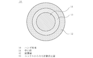
- the first aspect of the present invention is composed of a central core 11 made of silver and a coating layer 12 made of tin covering the central core 11, and between the central core 11 and the coating layer 12. It is the solder powder 10 in which the diffusion prevention layer 13 made of nickel is formed.
- the average particle size of the solder powder 10 is 1 ⁇ m or more and 30 ⁇ m or less, and the silver content is 10% by mass or more and 81% by mass or less with respect to 100% by mass of the total amount of the solder powder 10.
- a second aspect of the present invention is the invention based on the first aspect, wherein the thickness of the diffusion prevention layer made of nickel is 0.04 or more and 0.50 or less when the radius of the central core is 1. It is a ratio.
- the third aspect of the present invention is a method for preparing a solder paste by mixing the solder powder of the first or second aspect and a solder flux into a paste.
- a fourth aspect of the present invention is a method for mounting an electronic component using a solder paste prepared by the method of the third aspect.
- the solder powder according to the first aspect of the present invention is composed of a central core and a coating layer covering the central core, wherein the central core is made of silver and the coating layer is made of tin.
- a diffusion preventing layer made of nickel is formed, the average particle size of the solder powder is 1 ⁇ m or more and 30 ⁇ m or less, and the silver content is 10% by mass or more and 81% by mass or less with respect to 100% by mass of the total amount of solder powder. is there.
- the diffusion prevention layer made of nickel is interposed between the silver central core and the tin coating layer, the central core silver is not diffused into the tin of the coating layer.
- the thickness of the diffusion prevention layer made of nickel is a ratio of 0.04 or more and 0.50 or less when the radius of the central core is 1, so that the central core has Diffusion of the core core silver into the tin coating core and diffusion of the tin core core into silver during powder storage without significantly changing the solder properties of the solder powder comprising silver and the coating layer containing tin Can be prevented.
- solder paste prepared by the method of the third aspect of the present invention is obtained using the solder powder of the present invention. Therefore, this solder paste is rapidly melted during reflow and has excellent meltability.
- the solder paste of the present invention is used. Therefore, during reflow, the melting speed of the solder paste and the excellent meltability make it easy and highly accurate. It is possible to mount electronic components. In the joined body on which the electronic component is mounted, not only the coating layer but also the central core melts to form an Ag—Sn alloy or Sn—Ni—Ag alloy at the time of reflow, so that the formed Ag—Sn alloy or Sn—Ni is formed. -Due to the Ag alloy, even when exposed to a high temperature atmosphere after soldering, remelting and reduction in bonding strength are unlikely to occur.
- solder powder As shown in FIG. 1, the solder powder of this embodiment is composed of a central core 11 and a coating layer 12 covering the central core 11, the central core 11 is made of silver, the coating layer 12 is made of tin, and the center A diffusion preventing layer 13 made of nickel is provided between the core and the coating layer.
- the solder powder of the present embodiment has a structure in which the central core made of silver is coated with the coating layer made of tin having a low melting point, and thus has excellent meltability during reflow.
- silver and tin are contained in one metal particle constituting the powder, melting unevenness and composition shift during reflow hardly occur, and high bonding strength can be obtained.
- the solder powder has a diffusion preventing layer made of nickel between the central core and the coating layer, diffusion of silver into tin and diffusion of tin into silver can be prevented. Furthermore, after reflow, a bonding layer made of silver and an intermetallic compound having a high melting point such as Ag 3 Sn, Ag 4 Sn, Ni 3 Sn 4 , Ni 3 Sn 2 , Ni 3 Sn, NiSn 3 is formed. After reflow, remelting and reduction in bonding strength are unlikely to occur, and particularly suitable for electronic parts exposed to a high temperature atmosphere.
- the thickness of the diffusion prevention layer 13 made of nickel is preferably a ratio of 0.04 or more and 0.50 or less when the radius of the central core is 1, and a ratio of 0.05 or more and 0.20 or less. More preferably it is. If it is less than 0.04, it is difficult to prevent the diffusion of silver or tin, and if it exceeds 0.50, the meltability of the solder powder tends to decrease.
- the solder powder 10 of the present embodiment has an average particle size of 1 ⁇ m or more and 30 ⁇ m or less.
- the reason why the average particle size of the solder powder is limited to 1 ⁇ m or more and 30 ⁇ m or less is that when it exceeds 30 ⁇ m, the bump coplanarity is deteriorated when the bump is formed, and it is applied when the pattern surface is coated with solder. This is because unevenness occurs and the entire surface of the pattern cannot be uniformly coated.
- the average particle size of the solder powder is preferably in the range of 2 to 20 ⁇ m.
- the average particle diameter of the powder was measured by a particle size distribution measuring apparatus using a laser diffraction / scattering method (manufactured by Horiba, Ltd., laser diffraction / scattering particle diameter distribution measuring apparatus LA-950). Volume cumulative median diameter (Median diameter, D 50 ).
- An Sn—Ni—Ag alloy having an onset temperature is formed. Even if the silver content is small, after reflowing, a Sn—Ag alloy or Sn—Ni—Ag alloy having a higher solidification start temperature than tin is formed, but solidification starts by containing more silver.
- the temperature is further increased because the ratio of intermetallic compounds having a high melting point in the alloy is further increased. Thereby, in the solder bump formed by reflow of the solder paste containing this solder powder, the heat resistance is greatly improved, and remelting and reduction in bonding strength can be prevented. For this reason, it can be suitably used as a high-temperature solder used for mounting electronic components exposed to a high-temperature atmosphere.
- the content rate of the silver which occupies for 100 mass% of total amounts of powder shall be 10 to 51 mass%.
- the content ratio of nickel in the solder powder is 1% by mass or more and less than 15% by mass, preferably 2% by mass or more and 10% by mass or less with respect to 100% by mass of the total amount of the solder powder. According to this content ratio, the thickness of the diffusion preventing layer made of nickel is determined. If the nickel content is less than 1% by mass, it is difficult to prevent silver or tin from being diffused, and if it is 15% by mass or more, the meltability of the solder powder decreases.
- the content ratio of tin in the solder powder is 10% by mass or more and less than 80% by mass, preferably 15% by mass or more with respect to the balance other than the silver and nickel in the powder, that is, 100% by mass of the total amount of the solder powder. 70% by mass or less. This is because if the tin content is less than 10% by mass, the low melting point required for the solder powder is not exhibited during reflow.
- the content is 80% by mass or more, the silver content decreases as a result, and the heat resistance of the solder bump formed after reflowing is lowered. That is, when the solder after mounting is exposed to a high temperature atmosphere, the solder after mounting may be remelted or a liquid phase may be generated in a part of the solder, which may reduce the bonding strength with the substrate or the like.
- a silver powder dispersion is added to and mixed with a solvent to prepare a silver powder dispersion, and a compound containing nickel is added to and mixed with this to prepare a solution in which this compound is dissolved.
- the ratio of the silver powder and the nickel compound in the solution is adjusted so that the content ratio of each metal element is within the above range after the solder powder is manufactured.
- Examples of the solvent include water, alcohol, ether, ketone, ester and the like.
- Examples of the dispersant include cellulose-based, vinyl-based, and polyhydric alcohols.
- gelatin, casein, and the like can be used.
- the complexing agent By adding the complexing agent, the metal ion does not precipitate over a wide range of pH from acidic to alkaline, and synthesis in a wide pH range is possible.
- the complexing agent examples include succinic acid, tartaric acid, glycolic acid, lactic acid, phthalic acid, malic acid, citric acid, oxalic acid, ethylenediaminetetraacetic acid, iminodiacetic acid, nitrilotriacetic acid, and salts thereof.
- Reducing agents include phosphoric acid compounds such as sodium phosphinate, boron hydrides such as sodium tetrahydroborate and dimethylamine borane, nitrogen compounds such as hydrazine, metal ions such as trivalent titanium ions and divalent chromium ions. Etc.
- a reducing agent aqueous solution is added to the solution and mixed, whereby silver ions and nickel ions in the solution are reduced, and a dispersion in which metal powder is dispersed in the solution is obtained.
- a solution in which the compound containing silver and the compound containing nickel are dissolved is used, first, silver nobler than nickel is reduced, and then nickel is reduced.
- the reducing agent aqueous solution is dropped into the dissolving solution in the container at a predetermined addition rate and stirred with a stirrer or a reaction tube having a predetermined diameter. Examples include a method of pouring both solutions into a reaction tube at a predetermined flow rate and mixing them.
- this dispersion is subjected to solid-liquid separation by decantation or the like, and the collected solid content is washed with water or an aqueous solution whose pH is adjusted, or methanol, ethanol, acetone or the like. After washing, the solid content is recovered by solid-liquid separation again.
- the steps from washing to solid-liquid separation are preferably repeated 2 to 5 times.
- the collected solid content is vacuum-dried to form a metal powder with an Ag nucleus Ni layer composed of a central core made of silver and a nickel layer covering the central core.
- the starting silver powder preferably has an average particle size of 0.1 ⁇ m or more and 27 ⁇ m or less. Below this lower limit, the average particle size of the solder powder tends to be less than 1 ⁇ m, causing the above-mentioned problems, and it becomes difficult to make the content of silver constituting the solder powder 10% by mass or more. On the other hand, when the upper limit is exceeded, the average particle size of the solder powder tends to exceed 30 ⁇ m, resulting in the above-mentioned problems.
- the average particle size of the silver powder is more preferably 2 to 20 ⁇ m. This silver powder can be obtained not only by a chemical method using a reduction reaction but also by a physical method such as an atomizing method.
- the same reducing agent aqueous solution as the above-described reducing agent aqueous solution is added to and mixed with the above-mentioned dissolving solution, whereby nickel ions in the dissolving solution are reduced, and a dispersion in which metal powder is dispersed in the solution is obtained.
- This dispersion is subjected to solid-liquid separation by the same method as described above, and the collected solid content is washed by the same method as described above and vacuum dried to coat the central core made of silver and the central core.
- a metal powder with an Ag core Ni layer composed of a nickel layer is formed.
- the metal powder with Ag core Ni layer obtained by the above-described method and a dispersing agent are added and mixed in a solvent to prepare a dispersion of metal powder with Ag core Ni layer, and a compound containing tin is added thereto. Addition and mixing are performed to obtain a solution containing tin ions in which the metal powder with the Ag core Ni layer is decomposed.
- tin compounds include tin (II) chloride, tin (II) sulfate, tin (II) acetate, and tin (II) oxalate.
- the addition ratio of the compound containing tin is adjusted so that the content ratio of each metal element is within the above range after the solder powder is manufactured.
- the dispersion medium and the solvent the above-described dispersion medium and solvent are used.
- a dispersion is obtained in which a powder having a tin layer formed on the surface of a metal powder with an Ag core Ni layer is dispersed in the liquid. This dispersion is washed in the same manner as described above. After washing, the solid content is recovered by solid-liquid separation again. The steps from washing to solid-liquid separation are preferably repeated 2 to 5 times. The collected solid is vacuum dried to obtain a solder powder in which a metal powder with an Ag core Ni layer is coated with tin.
- solder paste and its preparation method The solder powder of the present embodiment obtained by the above steps is suitably used as a material for a solder paste obtained by mixing with a solder flux to form a paste.
- the solder paste is prepared by mixing solder powder and solder flux at a predetermined ratio to form a paste.
- the solder flux used for the preparation of the solder paste is not particularly limited, but a flux prepared by mixing components such as a solvent, rosin, thixotropic agent and activator can be used.
- Solvents suitable for the preparation of the solder flux include diethylene glycol monohexyl ether, diethylene glycol monobutyl ether, diethylene glycol monobutyl ether acetate, tetraethylene glycol, 2-ethyl-1,3-hexanediol, ⁇ -terpineol and the like having a boiling point of 180.
- An organic solvent having a temperature of not lower than ° C. can be mentioned.
- examples of the rosin include gum rosin, hydrogenated rosin, polymerized rosin, and ester rosin.
- thixotropic agents include hardened castor oil, fatty acid amide, natural fats and oils, synthetic fats and oils, N, N′-ethylenebis-12-hydroxystearylamide, 12-hydroxystearic acid, 1,2,3,4-dibenzylidene- And D-sorbitol and its derivatives.
- the activator is preferably a hydrohalic acid amine salt, specifically, triethanolamine, diphenylguanidine, ethanolamine, butylamine, aminopropanol, polyoxyethylene oleylamine, polyoxyethylene laurelamine, polyoxyethylene.
- the solder flux can be obtained by mixing the above components at a predetermined ratio.
- the proportion of the solvent in the total amount of flux of 100% by mass is preferably 30 to 60% by mass, the proportion of the thixotropic agent is 1 to 10% by mass, and the proportion of the activator is preferably 0.1 to 10% by mass. If the solvent ratio is less than the lower limit, the viscosity of the flux will be too high, so the viscosity of the solder paste using this will also increase accordingly, resulting in poor printability, such as poor solder filling and uneven coating. May cause malfunctions.
- the viscosity of the flux becomes too low, and the viscosity of the solder paste using the flux also decreases accordingly, which may cause a problem that the solder powder and the flux component settle and separate.
- the ratio of the thixotropic agent is less than the lower limit, the viscosity of the solder paste becomes too low, which may cause a problem that the solder powder and the flux component are settled and separated.
- the viscosity of the solder paste becomes too high, which may cause problems such as poor solderability and poor printability such as coating unevenness.
- the ratio of the activator is less than the lower limit value, the solder powder may not be melted and a sufficient bonding strength may not be obtained.
- the upper limit value is exceeded, the activator may become solder powder during storage. This may cause a problem that the storage stability of the solder paste is lowered.
- a viscosity stabilizer may be added to the solder flux. Examples of the viscosity stabilizer include polyphenols that can be dissolved in a solvent, phosphoric acid compounds, sulfur compounds, tocophenols, tocophenol derivatives, ascorbic acid, and ascorbic acid derivatives. If there are too many viscosity stabilizers, problems such as a decrease in the meltability of the solder powder may occur.
- the amount of solder flux mixed when preparing the solder paste is preferably such that the proportion of the flux in 100% by mass of the prepared paste is 5 to 30% by mass. If it is less than the lower limit, it becomes difficult to form a paste due to insufficient flux, while if it exceeds the upper limit, the content of the flux in the paste is too high and the content of metal is reduced, and solder bumps of the desired size when melting the solder This is because it becomes difficult to obtain.
- solder paste is made of the above-described solder powder of the present invention, melting at the time of reflow is fast and excellent in meltability, and after reflow, the melting solder powder forms an intermetallic compound having a high melting point, Since heat resistance increases, remelting due to heat hardly occurs. For this reason, the solder paste of the present invention can be suitably used for mounting electronic parts and the like exposed to a high temperature atmosphere.
- solder paste is solder paste is transferred to a predetermined position of the substrate, or the solder paste is printed at a predetermined position by a printing method.
- a chip element which is an electronic component is mounted on the transferred or printed paste.
- the solder powder is reflowed by holding in a reflow furnace in a nitrogen atmosphere at a temperature of 250 to 400 ° C. for 5 to 120 minutes.
- the chip and the substrate may be joined while being pressed.
- the chip element and the substrate are bonded to obtain a bonded body, and the electronic component is mounted on the substrate.
- Example 1 First, 4.92 ⁇ 10 ⁇ 3 mol of nickel sulfate (II), 1.1 ⁇ 10 ⁇ 3 mol of sodium phosphinate, and 3.88 ⁇ 10 ⁇ 4 mol of sodium citrate are added to 50 mL of water, and a stirrer is added. The mixture was stirred at a rotational speed of 300 rpm for 5 minutes to prepare a solution. After adjusting the pH of this solution to 5.0 with sulfuric acid, 0.2 g of polyvinyl alcohol 500 (polyvinyl alcohol having an average molecular weight of 500) was added as a dispersant, and the mixture was further stirred at a rotation speed of 300 rpm for 10 minutes.
- NiII nickel sulfate
- sodium phosphinate 3.88 ⁇ 10 ⁇ 4 mol of sodium citrate
- polyvinyl alcohol 500 polyvinyl alcohol having an average molecular weight of 500
- silver powder having an average particle size of 0.32 ⁇ m is dispersed.
- the dispersion was added and stirred at a rotational speed of 500 rpm for 10 minutes to obtain a dispersion in which nickel-coated silver powder having nickel deposited on the surface of the silver powder was dispersed.
- the dispersion was allowed to stand for 60 minutes, and the produced powder was allowed to settle.
- the supernatant was discarded, and 100 mL of water was added thereto, followed by stirring for 10 minutes at a rotational speed of 300 rpm, and washing was performed four times. . Finally, this is dried in a vacuum dryer, the average particle diameter is 1.2 ⁇ m, silver is the central core, nickel is the first coating layer (diffusion prevention layer), and tin is the second coating layer. Solder powder formed on each (outermost layer) was obtained.
- Examples 2 to 41, Comparative Examples 1 to 36 Also in Examples 2 to 41 and Comparative Examples 1 to 36, the particle size of the silver powder to be used, the addition amount of the silver powder, the addition amount of nickel sulfate (II and tin sulfate (II), and the ratio of other components should be adjusted.
- a solder powder was obtained in the same manner as in Example 1 except that the silver core nucleus radius, the thickness of the nickel diffusion preventing layer and the tin outermost layer, and the solder powder having a predetermined particle diameter were controlled.
- the sum of the average radius of the central core made of silver, the average thickness of the diffusion preventing layer made of nickel, and the average thickness of the coating layer made of tin was taken as the average radius of the solder powder. These average values are the average values of 30 solder powders.
- Average particle size of solder powder The particle size distribution was measured with a particle size distribution measuring device using a laser diffraction scattering method (Horiba, Ltd., laser diffraction / scattering type particle size distribution measuring device LA-950). The volume cumulative median diameter (Median diameter, D 50 ) was defined as the average particle diameter of the solder powder.
- the solder powder was embedded in a thermosetting epoxy resin, and the solder powder cross section was dry-polished Then, using an electron microscope (Scanning-Electron-Microscope, SEM), for each of 30 solder powders, the radius of the central core made of silver, the thickness of the diffusion prevention layer made of nickel, and the thickness of the coating layer made of tin The thickness was measured and the average value of each was obtained. Furthermore, the ratio of the average value of the thickness (the thickness of the diffusion prevention layer / the radius of the central core) was calculated from the thickness of the diffusion prevention layer made of nickel and the radius of the central core made of silver obtained from the above measurement.
- Cohesive strength 50% by mass of diethylene glycol monohexyl ether as a solvent, 46% by mass of polymerized rosin (softening point 95 ° C.) as rosin, and 1.0% by mass of cyclohexylamine hydrobromide as an activator
- a flux was prepared by mixing 3.0% by mass of hardened castor oil as a thixotropic agent. Next, this flux and the solder powders obtained in Examples 1 to 25 and Comparative Examples 1 to 12 were mixed at a ratio of 88 mass% flux and 12 mass% solder powder to obtain solder pastes, respectively. Prepared.
- the paste prepared above was transferred to a predetermined position on a 0.5 mm thick Kovar (Fe—Ni—Co alloy) substrate using a pin having a diameter of 100 ⁇ m by a pin transfer method.
- the Kovar substrate was Ni-plated, and further Au flash-plated.
- a 0.9 mm ⁇ LED chip was mounted on the transferred paste.
- the LED chip and the substrate are pressed at a pressure of 1.0 MPa, and reflowed at a predetermined maximum holding temperature in a nitrogen atmosphere in an infrared heating furnace for 0.17 hours, and the LED A bonded sample was obtained by bonding the chip and the Kovar substrate.
- the maximum holding temperature at the time of the reflow was set to different temperatures of 250 ° C., 300 ° C., and 350 ° C., and three bonded samples were obtained for each of the examples or comparative examples.
- Comparative Example 1 the average particle size of the solder powder was too small at 0.5 ⁇ m, and the solder powder did not melt before storing the solder powder due to the influence of the oxide film on the powder surface.
- Comparative Examples 2, 4, 5, 7 to 9, 11 to 14, 16 to 18, 23, 29, 33, and 35 the silver content is about 5% by mass, which is too low, and the solidification start temperature is sufficiently low. Since the heat resistance was not obtained, the bonding strength was not possible at the reflow temperatures of 350 ° C. before storing the solder powder and after storing for 30 days.
- Comparative Examples 3, 6, 10, 15, and 28 the silver content is too high at about 83% by mass, the solidification start temperature becomes too high, and the solder powder is reflowed at 250 ° C.
- the solder did not melt at the time of reflowing at 300 ° C. after storage for 30 days, and the bonding strength was not possible.
- the average particle size of the solder powder was about 40 ⁇ m, which was too large, and after reflowing, it became a bonding layer having large voids (voids), and a dense bonding layer was not obtained. For this reason, the bonding strength was not possible at a reflow temperature of 250 ° C., 300 ° C., or 350 ° C. before storing the solder powder and after storing for 30 days.
- the average particle size of the solder powder is in the range of 1 ⁇ m to 30 ⁇ m, and the silver content is in the range of 10% to 81% by mass with respect to 100% by mass of the total amount of the solder powder.
- the bonding strength was good, good or excellent at all reflow temperatures of 250 ° C., 300 ° C., and 350 ° C. before and after storing the solder powder for 30 days.
- the present invention can be suitably used for solder powder that may be stored for a long period of time. Moreover, it can utilize suitably for mounting of electronic components, especially mounting of electronic components exposed to a high temperature atmosphere.
Landscapes
- Engineering & Computer Science (AREA)
- Mechanical Engineering (AREA)
- Chemical & Material Sciences (AREA)
- Materials Engineering (AREA)
- Metallurgy (AREA)
- Organic Chemistry (AREA)
- Manufacturing & Machinery (AREA)
- Microelectronics & Electronic Packaging (AREA)
- Powder Metallurgy (AREA)
- Electric Connection Of Electric Components To Printed Circuits (AREA)
Abstract
本発明のハンダ粉末(10)は、銀からなる中心核(11)と、中心核(11)を被覆する錫からなる被覆層(12)と、中心核と被覆層の間にニッケルからなる拡散防止層(13)とにより構成される。このハンダ粉末(10)の平均粒径は、1μm以上30μm以下であり、このハンダ粉末(10)の全体量100質量%に対する銀の含有割合は、10質量%以上81質量%以下である。 また、本発明のハンダ粉末(10)は、更に、前記ニッケルからなる拡散防止層(13)の厚さを、前記中心核(11)の半径を1とするときに0.04以上0.50以下の比率とする。 また、本発明のハンダ用ペーストを調整する方法は、本発明のハンダ粉末(10)とハンダ用フラックスを混合してペースト化することによりハンダ用ペーストを調整する方法である。
Description
本発明は、電子部品等の実装に用いられる、中心核が銀からなり、被覆層が錫からなるハンダ粉末及びこの粉末を用いたハンダ用ペーストの調製方法に関する。なお、本国際出願は、2015年12月1日に出願した日本国特許出願第234641号(特願2015-234641)に基づく優先権を主張するものであり、特願2015-234641の全内容を本国際出願に援用する。
従来、中心核が銀からなり、被覆層が錫からなる、平均粒径が5μm以下のハンダ粉末が開示されている(例えば、特許文献1参照。)。このハンダ粉末は、環境の面から鉛フリーであって、微細であるため、印刷性に優れる。また中心核を構成する金属元素を銀とすることにより、リフロー時に被覆層のみならず中心核が溶融してAg-Sn合金を形成するため、形成されるAg-Sn合金により、ハンダの機械的強度が向上する。
しかしながら、特許文献1に記載された中心核が銀からなり、被覆層が錫からなるハンダ粉末は、ハンダ粉末を製造後、長期間保管すると、銀の錫への拡散係数が大きいため、中心核の銀が被覆層の錫に拡散し、中心核と被覆層の間にAg3Sn及び/又はAg4Snの融点の高い金属間化合物層を形成するか、又は中心核のすべての銀が被覆層の錫中に拡散し被覆層全体又は被覆層の一部が銀と錫との金属間化合物となるおそれがあった。被覆層全体又は被覆層の一部がこの種の金属間化合物層を形成したハンダ粉末は、上記金属間化合物を有しないハンダ粉末と比較して凝固開始温度が上昇する。このため、長期間保管したハンダ粉末と、保管前又は保管期間の短いハンダ粉末とは、上記金属間化合物の有無の違い又は上記金属間化合物の形成量の違いにより、凝固開始温度に差異を生じ、長期間保管したハンダ粉末を、保管前又は保管期間の短いハンダ粉末が溶融する温度で、リフローさせた場合、リフロー時の溶融ムラや溶融性不良による接合不良を生じることがあった。
本発明の第1の目的は、粉末保管時に中心核の銀の被覆層への拡散やこの被覆層の錫の中心核への拡散が抑制されたハンダ粉末及びこの粉末を用いたハンダ用ペーストを提供することにある。また本発明の第2の目的は、長期間保管したハンダ粉末を、保管前又は保管期間の短いハンダ粉末が溶融する温度で、リフローさせても、ハンダが十分に溶融しないことに起因した接合不良を生じないハンダ粉末及びこの粉末を用いたハンダ用ペーストを提供することにある。また本発明の第3の目的は、リフロー後、再溶融及び接合強度の低下が起こりにくく、特に高温雰囲気に晒される電子部品等の実装に好適なハンダ粉末及びこの粉末を用いたハンダ用ペーストの調製方法を提供することにある。
本発明者が鋭意研究を重ねた結果、ニッケル中での銀及び錫の拡散係数は非常に小さいことから、ニッケルを銀の中心核と錫の被覆層の間に拡散防止層として介装させれば、銀の錫への拡散は勿論、錫の銀への拡散も防止できることを見い出し、本発明に到達した。
本発明の第1の観点は、図1に示すように、銀からなる中心核11と中心核11を被覆する錫からなる被覆層12で構成され、中心核11と被覆層12の間にはニッケルからなる拡散防止層13が形成されたハンダ粉末10であることを特徴とする。ハンダ粉末10の平均粒径は1μm以上30μm以下であり、ハンダ粉末10の全体量100質量%に対し、銀の含有割合が10質量%以上81質量%以下である。
本発明の第2の観点は、第1の観点に基づく発明であって、ニッケルからなる拡散防止層の厚さが前記中心核の半径を1とするときに0.04以上0.50以下の比率であることを特徴とする。
本発明の第3の観点は、第1又は第2の観点のハンダ粉末とハンダ用フラックスを混合してペースト化することによりハンダ用ペーストを調製する方法である。
本発明の第4の観点は、第3の観点の方法により調製されたハンダ用ペーストを用いて電子部品を実装する方法である。
本発明の第1の観点のハンダ粉末は、中心核と中心核を被覆する被覆層で構成され、中心核が銀からなり、被覆層が錫からなるハンダ粉末において、中心核と被覆層の間にニッケルからなる拡散防止層が形成され、ハンダ粉末の平均粒径が1μm以上30μm以下であり、ハンダ粉末の全体量100質量%に対し、銀の含有割合が10質量%以上81質量%以下である。このように、本発明のハンダ粉末では、銀の中心核と錫の被覆層の間にニッケルからなる拡散防止層が介装されるので、中心核の銀が被覆層の錫に拡散することは勿論、被覆層の錫が中心核の銀に拡散することを防止できる。この結果、長期間保管したハンダ粉末を、保管前又は保管期間の短いハンダ粉末が溶融する温度で、リフローさせても、ハンダが十分に溶融しないことに起因した接合不良を生じることがない優れた効果を奏する。また、リフロー後は、Ag3Sn、Ag4Sn、Ni3Sn4、Ni3Sn2、Ni3Sn、NiSn3等の融点の高い金属間化合物及び銀からなる接合層が形成されるため、リフロー後、再溶融及び接合強度の低下が起こりにくく、特に高温雰囲気に晒される電子部品等に好適に実装される。
本発明の第2の観点のハンダ粉末は、ニッケルからなる拡散防止層の厚さが前記中心核の半径を1とするときに0.04以上0.50以下の比率であるため、中心核が銀からなり、被覆層が錫を含むハンダ粉末のハンダ特性を大幅に変えることなく、粉末保管時に中心核の銀の被覆層の錫への拡散及び被覆層の錫の中心核の銀への拡散を防止することができる。
本発明の第3の観点の方法により調製されたハンダ用ペーストは、上記本発明のハンダ粉末を用いて得られる。そのため、このハンダ用ペーストは、リフロー時の溶融が速く、溶融性に優れる。
本発明の第4の観点の電子部品を実装する方法では、上記本発明のハンダ用ペーストを用いるため、リフロー時にはハンダ用ペーストの溶融の速さ、優れた溶融性により、簡便に、かつ高い精度で電子部品を実装することができる。この電子部品を実装した接合体は、リフロー時に被覆層のみならず中心核が溶融してAg-Sn合金又はSn-Ni-Ag合金を形成するため、形成されるAg-Sn合金又はSn-Ni-Ag合金により、ハンダ接合後に高温雰囲気に晒されても、再溶融及び接合強度の低下が起こりにくい。
次に本発明を実施するための形態を図面に基づいて説明する。
〔ハンダ粉末〕
本実施形態のハンダ粉末は、図1に示すように、中心核11と中心核11を被覆する被覆層12で構成され、中心核11が銀からなり、被覆層12が錫からなり、かつ中心核と被覆層の間にニッケルからなる拡散防止層13を有する。本実施形態のハンダ粉末は、このように、銀からなる中心核が、融点の低い錫からなる被覆層で被覆された構造になっているため、リフロー時の溶融性に優れる。また、粉末を構成する一つの金属粒子内において、銀と錫が含まれるため、リフロー時の溶融ムラや組成ズレが起こりにくく、高い接合強度が得られる。更に、ハンダ粉末が中心核と被覆層の間にニッケルからなる拡散防止層を有するため、銀の錫への拡散及び錫の銀への拡散を防止することができる。更に、リフロー後は、Ag3Sn、Ag4Sn、Ni3Sn4、Ni3Sn2、Ni3Sn、NiSn3等の融点の高い金属間化合物及び銀からなる接合層が形成されるため、リフロー後、再溶融及び接合強度の低下が起こりにくく、特に高温雰囲気に晒される電子部品等に好適に実装される。
本実施形態のハンダ粉末は、図1に示すように、中心核11と中心核11を被覆する被覆層12で構成され、中心核11が銀からなり、被覆層12が錫からなり、かつ中心核と被覆層の間にニッケルからなる拡散防止層13を有する。本実施形態のハンダ粉末は、このように、銀からなる中心核が、融点の低い錫からなる被覆層で被覆された構造になっているため、リフロー時の溶融性に優れる。また、粉末を構成する一つの金属粒子内において、銀と錫が含まれるため、リフロー時の溶融ムラや組成ズレが起こりにくく、高い接合強度が得られる。更に、ハンダ粉末が中心核と被覆層の間にニッケルからなる拡散防止層を有するため、銀の錫への拡散及び錫の銀への拡散を防止することができる。更に、リフロー後は、Ag3Sn、Ag4Sn、Ni3Sn4、Ni3Sn2、Ni3Sn、NiSn3等の融点の高い金属間化合物及び銀からなる接合層が形成されるため、リフロー後、再溶融及び接合強度の低下が起こりにくく、特に高温雰囲気に晒される電子部品等に好適に実装される。
ニッケルからなる拡散防止層13は、その厚さが中心核の半径を1とするときに0.04以上0.50以下の比率であることが好ましく、0.05以上0.20以下の比率であることが更に好ましい。0.04未満では銀又は錫の拡散を防止することが困難であり、0.50を超えるとハンダ粉末の溶融性が低下し易い。
本実施形態のハンダ粉末10は、平均粒径が1μm以上30μm以下である。ハンダ粉末の平均粒径を1μm以上30μm以下に限定したのは、30μmを越えるとバンプを形成する場合においてバンプのコプラナリティが低下するという不具合を生じ、また、パターン表面をハンダでコートする場合に塗布ムラが生じ、パターン全面を均一にコートできないという不具合を生じるからである。なお、1μm未満になると、比表面積が高くなり、粉末の表面酸化層の影響によりハンダの溶融性が低下する。ハンダ粉末の平均粒径は2~20μmの範囲とするのが好ましい。なお、本明細書において、粉末の平均粒径とは、レーザー回折散乱法を用いた粒度分布測定装置(堀場製作所社製、レーザー回折/散乱式粒子径分布測定装置LA-950)にて測定した体積累積中位径(Median径、D50)をいう。
また、本実施形態のハンダ粉末10は、粉末の全体量100質量%に対し、銀の含有割合が10質量%以上81質量%以下である。従来のハンダ粉末では、Sn-Pb系共晶ハンダ(組成比 Sn:Pb=63:37質量%)の代替として使用されるため、融点が近く、共晶組成が求められるという理由から、銀の割合を1.0~3.5質量%程度と、比較的少なめに含有させている。一方、本実施形態のハンダ粉末では、これより多めの上記範囲で含ませることにより、リフロー後に、880~600℃程度の高い凝固開始温度を有するSn-Ag合金又は800~450℃程度の高い凝固開始温度を有するSn-Ni-Ag合金を形成する。なお、銀の含有割合が少なくても、リフロー後は、錫よりも凝固開始温度の高いSn-Ag合金又はSn-Ni-Ag合金を形成するが、銀をより多く含有させることで、凝固開始温度が更に上昇するのは、合金中に高い融点を有する金属間化合物の比率がより一層高くなるという理由からである。これにより、このハンダ粉末を含むハンダ用ペーストのリフローによって形成されるハンダバンプでは、耐熱性が大幅に向上し、再溶融及び接合強度の低下を防止することができる。このため、特に高温雰囲気に晒される電子部品等の実装に用いられる高温ハンダとして好適に用いることができる。銀の含有割合が10質量%未満では、凝固開始温度が低くなることから、リフロー後に形成されるハンダバンプにおいて十分な耐熱性が得られず、高温雰囲気での使用の際に再溶融が起こり、高温ハンダとして用いることができない。一方、81質量%を越えると凝固開始温度が高くなりすぎて、ハンダが十分に溶融しないため、接合不良が発生するという不具合が生じる。このうち、粉末の全体量100質量%に占める銀の含有割合は、10質量%以上51質量%以下とするのが好ましい。
また、ハンダ粉末中のニッケルの含有割合は、ハンダ粉末の全体量100質量%に対して1質量%以上15質量%未満、好ましくは2質量%以上10質量%以下である。この含有割合に応じて、前述したニッケルからなる拡散防止層の厚さが決められる。ニッケルの含有割合が1質量%未満では銀又は錫の拡散を防止することが困難であり、15質量%以上では、ハンダ粉末の溶融性が低下するという不具合を生じる。
更に、ハンダ粉末中の錫の含有割合は、粉末中の上記銀及びニッケル以外の残部、即ちハンダ粉末の全体量100質量%に対して10質量%以上80質量%未満、好ましくは15質量%以上70質量%以下である。錫の含有割合が10質量%未満では、リフロー時においてハンダ粉末に必要とされる低融点を示さないからである。また、80質量%以上では、結果的に銀の含有割合が少なくなり、リフロー後に形成されるハンダバンプの耐熱性が低下する。即ち、高温雰囲気に実装後のハンダが晒されると実装後のハンダが再溶融するか、又はハンダの一部において液相が生じて、基板等との接合強度が低下するおそれがある。
〔ハンダ粉末の製造方法〕
続いて、ハンダ粉末中の銀の含有割合に応じた本実施形態のハンダ粉末の製造方法について説明する。
続いて、ハンダ粉末中の銀の含有割合に応じた本実施形態のハンダ粉末の製造方法について説明する。
先ず、銀粉末と分散剤を溶媒に添加混合して銀粉末の分散液を調製し、これに上記ニッケルを含む化合物を添加混合しこの化合物が溶解した溶解液を調製する。溶解液中における銀粉末及びニッケル化合物の割合は、ハンダ粉末製造後に、各金属元素の含有割合が上記範囲になるように調整する。
溶媒としては、水、アルコール、エーテル、ケトン、エステル等が挙げられる。また、分散剤としては、セルロース系、ビニル系、多価アルコール等が挙げられ、その他にゼラチン、カゼイン等を用いることができる。なお、溶媒に上記金属化合物をそれぞれ添加して溶解させた後、錯化剤を加えて、各金属元素を錯体化した後に、分散剤を添加してもよい。錯化剤を加えることでpHが酸性からアルカリ側の広い範囲にわたり、金属イオンが沈殿せず、広いpHの範囲での合成が可能となる。錯化剤としては、コハク酸、酒石酸、グリコール酸、乳酸、フタル酸、リンゴ酸、クエン酸、シュウ酸、エチレンジアミン四酢酸、イミノ二酢酸、ニトリロ三酢酸又はその塩等が挙げられる。
次いで、還元剤を溶解した水溶液を調製し、この水溶液のpHを、上記調製した溶解液と同程度に調整する。還元剤としては、ホスフィン酸ナトリウム等のリン酸系化合物、テトラヒドロホウ酸ナトリウム、ジメチルアミンボラン等のホウ素水素化物、ヒドラジン等の窒素化合物、三価のチタンイオンや2価のクロムイオン等の金属イオン等が挙げられる。
次に、上記溶解液に還元剤水溶液を添加して混合することにより、溶解液中の銀イオン、ニッケルイオンが還元され、液中に金属粉末が分散した分散液が得られる。この還元反応では、上記銀を含む化合物、ニッケルを含む化合物が溶解する溶解液を用いているので、先ず、ニッケルよりも貴な銀が還元され、続いてニッケルが還元される。溶解液と還元剤水溶液を混合する方法としては、容器内の溶解液に所定の添加速度で還元剤水溶液を滴下し、スターラ等で攪拌する方法や、所定の径を有する反応チューブを用い、この反応チューブ内に両液を所定の流量で注ぎ込み、混合させる方法等が挙げられる。
次に、この分散液を、デカンテーション等によって固液分離し、回収した固形分を水又はpHを調整した水溶液、或いはメタノール、エタノール、アセトン等で洗浄する。洗浄後は、再度固液分離して固形分を回収する。洗浄から固液分離までの工程を、好ましくは2~5回繰り返す。回収した固形分を真空乾燥させることにより、銀からなる中心核と、この中心核を被覆するニッケル層で構成されたAg核Ni層付きの金属粉末を形成する。
出発原料の銀粉末は、0.1μm以上27μm以下の平均粒径を有することが好ましい。この下限値未満では、ハンダ粉末の平均粒径が1μm未満になり易く、上述した不具合を生じ、またハンダ粉末を構成する銀の含有量10質量%以上にすることが困難になる。また上限値を超えると、ハンダ粉末の平均粒径が30μmを超え易くなり、上述した不具合を生じる。銀粉末の平均粒径は2~20μmであることが更に好ましい。この銀粉末は、還元反応による化学的手法で得られる他、アトマイズ法のような物理的手法によって得られる。
次に、上記溶解液に上述した還元剤水溶液と同じ還元剤水溶液を添加して混合することにより、溶解液中のニッケルイオンが還元され、液中に金属粉末が分散した分散液が得られる。この分散液を、上述した方法と同じ方法で固液分離し、回収した固形分を上述した方法と同じ方法で洗浄し真空乾燥させることにより、銀からなる中心核と、この中心核を被覆するニッケル層で構成されたAg核Ni層付きの金属粉末を形成する。
続いて、上述した方法で得られたAg核Ni層付きの金属粉末と分散剤を溶媒に添加混合してAg核Ni層付きの金属粉末の分散液を調製し、これに錫を含む化合物を添加混合してAg核Ni層付きの金属粉末が分解した錫イオンを含む溶解液を得る。錫化合物としては、塩化錫(II)、硫酸錫(II)、酢酸錫(II)、シュウ酸錫(II)等が挙げられる。錫を含む化合物の添加割合は、ハンダ粉末製造後に、各金属元素の含有割合が上記範囲になるように調整する。分散媒及び溶媒には、上述した分散媒及び溶媒が用いられる。
更に続いて、上記錫イオンを含む溶解液に上述した還元剤と同じ還元剤を溶解した還元剤水溶液を上述した方法と同じ方法で添加混合することにより、溶解液中の錫イオンが還元され、液中にAg核Ni層付きの金属粉末の表面に錫層が形成された粉末が分散した分散液を得る。この分散液を、上述した方法と同じ方法で洗浄する。洗浄後は、再度固液分離して固形分を回収する。洗浄から固液分離までの工程を、好ましくは2~5回繰り返す。回収した固形分を真空乾燥させることにより、Ag核Ni層付きの金属粉末を錫が被覆したハンダ粉末が得られる。
〔ハンダ用ペースト及びその調製方法〕
以上の工程により、得られた本実施形態のハンダ粉末は、ハンダ用フラックスと混合してペースト化して得られるハンダ用ペーストの材料として好適に用いられる。ハンダ用ペーストの調製は、ハンダ粉末とハンダ用フラックスとを所定の割合で混合してペースト化することにより行われる。ハンダ用ペーストの調製に用いられるハンダ用フラックスは、特に限定されないが、溶剤、ロジン、チキソ剤及び活性剤等の各成分を混合して調製されたフラックスを用いることができる。
以上の工程により、得られた本実施形態のハンダ粉末は、ハンダ用フラックスと混合してペースト化して得られるハンダ用ペーストの材料として好適に用いられる。ハンダ用ペーストの調製は、ハンダ粉末とハンダ用フラックスとを所定の割合で混合してペースト化することにより行われる。ハンダ用ペーストの調製に用いられるハンダ用フラックスは、特に限定されないが、溶剤、ロジン、チキソ剤及び活性剤等の各成分を混合して調製されたフラックスを用いることができる。
上記ハンダ用フラックスの調製に好適な溶剤としては、ジエチレングリコールモノヘキシルエーテル、ジエチレングリコールモノブチルエーテル、ジエチレングリコールモノブチルエーテルアセテート、テトラエチレングリコール、2-エチル-1,3-ヘキサンジオール、α-テルピネオール等の沸点が180℃以上である有機溶剤が挙げられる。また、ロジンとしては、ガムロジン、水添ロジン、重合ロジン、エステルロジン等が挙げられる。
また、チキソ剤としては、硬化ひまし油、脂肪酸アマイド、天然油脂、合成油脂、N,N’-エチレンビス-12-ヒドロキシステアリルアミド、12-ヒドロキシステアリン酸、1,2,3,4-ジベンジリデン-D-ソルビトール及びその誘導体等が挙げられる。
また、活性剤としては、ハロゲン化水素酸アミン塩が好ましく、具体的には、トリエタノールアミン、ジフェニルグアニジン、エタノールアミン、ブチルアミン、アミノプロパノール、ポリオキシエチレンオレイルアミン、ポリオキシエチレンラウレルアミン、ポリオキシエチレンステアリルアミン、ジエチルアミン、トリエチルアミン、メトキシプロピルアミン、ジメチルアミノプロピルアミン、ジブチルアミノプロピルアミン、エチルヘキシルアミン、エトキシプロピルアミン、エチルヘキシルオキシプロピルアミン、ビスプロピルアミン、イソプロピルアミン、ジイソプロピルアミン、ピペリジン、2,6-ジメチルピペリジン、アニリン、メチルアミン、エチルアミン、ブチルアミン、3-アミノ-1-プロペン、イソプロピルアミン、ジメチルヘキシルアミン、シクロヘキシルアミン等のアミンの塩化水素酸塩又は臭化水素酸塩が挙げられる。
ハンダ用フラックスは、上記各成分を所定の割合で混合することにより得られる。フラックス全体量100質量%中に占める溶剤の割合は30~60質量%、チキソ剤の割合は1~10質量%、活性剤の割合は0.1~10質量%とするのが好ましい。溶剤の割合が下限値未満では、フラックスの粘度が高くなりすぎるため、これを用いたハンダ用ペーストの粘度も応じて高くなり、ハンダの充填性低下や塗布ムラが多発する等、印刷性が低下する不具合を生じる場合がある。一方、上限値を越えるとフラックスの粘度が低くなりすぎるため、これを用いたハンダ用ペーストの粘度も応じて低くなることから、ハンダ粉末とフラックス成分が沈降分離する不具合を生じる場合がある。また、チキソ剤の割合が下限値未満では、ハンダ用ペーストの粘度が低くなりすぎるため、ハンダ粉末とフラックス成分が沈降分離するという不具合を生じる場合がある。一方、上限値を越えるとハンダ用ペーストの粘度が高くなりすぎるため、ハンダ充填性や塗布ムラ等の印刷性低下という不具合を生じる場合がある。
また、活性剤の割合が下限値未満では、ハンダ粉末が溶融せず、十分な接合強度が得られないという不具合を生じる場合があり、一方、上限値を越えると保管中に活性剤がハンダ粉末と反応し易くなるため、ハンダ用ペーストの保存安定性が低下するという不具合を生じる場合がある。この他、ハンダ用フラックスには、粘度安定剤を添加しても良い。粘度安定剤としては、溶剤に溶解可能なポリフェノール類、リン酸系化合物、硫黄系化合物、トコフェノール、トコフェノールの誘導体、アルコルビン酸、アルコルビン酸の誘導体等が挙げられる。粘度安定剤は、多すぎるとハンダ粉末の溶融性が低下する等の不具合が生じる場合があるため、10質量%以下とするのが好ましい。
ハンダ用ペーストを調製する際のハンダ用フラックスの混合量は、調製後のペースト100質量%中に占める該フラックスの割合が5~30質量%になる量にするのが好ましい。下限値未満ではフラックス不足でペースト化が困難になり、一方、上限値を越えるとペースト中のフラックスの含有割合が多すぎて金属の含有割合が少なくなってしまい、ハンダ溶融時に所望のサイズのハンダバンプを得るのが困難になるからである。
このハンダ用ペーストは、上記本発明のハンダ粉末を材料としているため、リフロー時の溶融が速く、溶融性に優れる一方、リフロー後は、溶融するハンダ粉末が融点の高い金属間化合物を形成し、耐熱性が上昇するため、熱による再溶融が起こりにくい。このため、本発明のハンダ用ペーストは、特に高温雰囲気に晒される電子部品等の実装に好適に用いることができる。
〔ハンダ用ペーストを用いた電子部品の実装方法と接合体〕
上述した方法で調製されたハンダ用ペーストを用いてシリコンチップ、LEDチップ等の電子部品を各種放熱基板、FR4(Flame Retardant Type 4)基板、コバール等の基板に実装するには、ピン転写法にて上記基板の所定位置にハンダ用ペーストを転写するか、又は印刷法により所定位置にハンダ用ペーストを印刷する。次いで、転写又は印刷されたペースト上に電子部品であるチップ素子を搭載する。この状態で、リフロー炉にて窒素雰囲気中、250~400℃の温度で、5~120分間保持して、ハンダ粉末をリフローする。場合によっては、チップと基板とを加圧しながら接合してもよい。これにより、チップ素子と基板とを接合させて接合体を得て、電子部品を基板に実装する。
上述した方法で調製されたハンダ用ペーストを用いてシリコンチップ、LEDチップ等の電子部品を各種放熱基板、FR4(Flame Retardant Type 4)基板、コバール等の基板に実装するには、ピン転写法にて上記基板の所定位置にハンダ用ペーストを転写するか、又は印刷法により所定位置にハンダ用ペーストを印刷する。次いで、転写又は印刷されたペースト上に電子部品であるチップ素子を搭載する。この状態で、リフロー炉にて窒素雰囲気中、250~400℃の温度で、5~120分間保持して、ハンダ粉末をリフローする。場合によっては、チップと基板とを加圧しながら接合してもよい。これにより、チップ素子と基板とを接合させて接合体を得て、電子部品を基板に実装する。
次に本発明の実施例を比較例とともに詳しく説明する。
<実施例1>
先ず、水50mLに硫酸ニッケル(II)を4.92×10⁻³mol、ホスフィン酸ナトリウムを1.1×10⁻³mol、クエン酸ナトリウムを3.88×10⁻⁴molを加え、スターラを用いて回転速度300rpmにて5分間攪拌し、溶解液を調製した。この溶解液を硫酸にてpHを5.0に調整した後、分散剤としてポリビニルアルコール500(平均分子量が500のポリビニルアルコール)を0.2g加え、更に回転速度300rpmにて10分間攪拌した。次いで、この溶解液に、水50mLに分散剤としてポリビニルアルコール500(平均分子量が500のポリビニルアルコール)を0.2g溶解し、かつ、平均粒径が0.32μmの銀粉末3.41gを分散させた分散液を添加し、回転速度500rpmにて10分間攪拌し、銀粉末表面にニッケルを析出させたニッケル被覆銀粉末が分散する分散液を得た。この分散液を60分間静置して生成した粉末を沈降させた後、上澄み液を捨て、ここに水100mLを加えて回転速度300rpmにて10分間攪拌する操作を4回繰返し、洗浄を行った。最後にこれを真空乾燥機にて乾燥することにより、銀を中心核に、ニッケルを第1被覆層(拡散防止層)とする粉末を得た。
先ず、水50mLに硫酸ニッケル(II)を4.92×10⁻³mol、ホスフィン酸ナトリウムを1.1×10⁻³mol、クエン酸ナトリウムを3.88×10⁻⁴molを加え、スターラを用いて回転速度300rpmにて5分間攪拌し、溶解液を調製した。この溶解液を硫酸にてpHを5.0に調整した後、分散剤としてポリビニルアルコール500(平均分子量が500のポリビニルアルコール)を0.2g加え、更に回転速度300rpmにて10分間攪拌した。次いで、この溶解液に、水50mLに分散剤としてポリビニルアルコール500(平均分子量が500のポリビニルアルコール)を0.2g溶解し、かつ、平均粒径が0.32μmの銀粉末3.41gを分散させた分散液を添加し、回転速度500rpmにて10分間攪拌し、銀粉末表面にニッケルを析出させたニッケル被覆銀粉末が分散する分散液を得た。この分散液を60分間静置して生成した粉末を沈降させた後、上澄み液を捨て、ここに水100mLを加えて回転速度300rpmにて10分間攪拌する操作を4回繰返し、洗浄を行った。最後にこれを真空乾燥機にて乾燥することにより、銀を中心核に、ニッケルを第1被覆層(拡散防止層)とする粉末を得た。
引続き、水50mLに上記粉末0.37gを分散させて分散液を調製した。この分散液に硫酸錫(II)2.56×10⁻²molを加え、スターラを用いて回転速度300rpmにて5分間撹拌し、混合液を調製した。この混合液を硫酸にてpHを0.5に調整した後、分散剤としてポリビニルアルコール500(平均分子量が500のポリビニルアルコール)を0.5g加え、更に回転速度300rpmにて10分間撹拌した。次いで、この混合液にpHを0.5に調整した1.58mol/Lの2価クロムイオン水溶液50mLを、添加速度50mL/minにて加え、回転速度500rpmにて10分間撹拌して錫イオンを還元することにより、ニッケル被覆銀粉末表面に錫を析出させた最外層が錫からなるニッケル被覆銀粉末が分散する分散液を得た。この分散液を60分間静置して生成した粉末を沈降させた後、上澄み液を捨て、ここに水100mLを加えて回転速度300rpmにて10分間攪拌する操作を4回繰返し、洗浄を行った。最後にこれを真空乾燥機にて乾燥することにより、平均粒径が1.2μmであって、銀を中心核に、ニッケルを第1被覆層(拡散防止層)に、錫を第2被覆層(最外層)にそれぞれ形成したハンダ粉末を得た。
<実施例2~41、比較例1~36>
実施例2~41、比較例1~36においても、用いる銀粉末の粒径及び銀粉末の添加量、硫酸ニッケル(II及び硫酸錫(II)の添加量、並びに他成分の割合を調整することにより、所定の銀中心核半径、ニッケル拡散防止層及び錫最外層の厚さ、更には所定の粒径のハンダ粉末に制御したこと以外は、実施例1と同様にしてハンダ粉末を得た。
実施例2~41、比較例1~36においても、用いる銀粉末の粒径及び銀粉末の添加量、硫酸ニッケル(II及び硫酸錫(II)の添加量、並びに他成分の割合を調整することにより、所定の銀中心核半径、ニッケル拡散防止層及び錫最外層の厚さ、更には所定の粒径のハンダ粉末に制御したこと以外は、実施例1と同様にしてハンダ粉末を得た。
<比較試験及び評価>
実施例1~41及び比較例1~36で得られたハンダ粉末について、次に述べる方法により、ハンダ粉末の銀の含有割合[質量%]、平均粒径[μm]、銀からなる中心核の平均半径[μm]、ニッケルからなる拡散防止層の平均厚さ[μm]、錫からなる被覆層の平均厚さ[μm]を測定した。これらの結果を以下の表1~表4に示す。また、これらのハンダ粉末を用いてハンダ用ペーストをそれぞれ調製し、リフロー時の最大保持温度を変えたときの接合強度を評価した。これらの結果を以下の表5~表8に示す。なお、銀からなる中心核の平均半径と、ニッケルからなる拡散防止層の平均厚さと、錫からなる被覆層の平均厚さとの和をハンダ粉末の平均半径とした。これらの平均値は30個のハンダ粉末の平均値である。
実施例1~41及び比較例1~36で得られたハンダ粉末について、次に述べる方法により、ハンダ粉末の銀の含有割合[質量%]、平均粒径[μm]、銀からなる中心核の平均半径[μm]、ニッケルからなる拡散防止層の平均厚さ[μm]、錫からなる被覆層の平均厚さ[μm]を測定した。これらの結果を以下の表1~表4に示す。また、これらのハンダ粉末を用いてハンダ用ペーストをそれぞれ調製し、リフロー時の最大保持温度を変えたときの接合強度を評価した。これらの結果を以下の表5~表8に示す。なお、銀からなる中心核の平均半径と、ニッケルからなる拡散防止層の平均厚さと、錫からなる被覆層の平均厚さとの和をハンダ粉末の平均半径とした。これらの平均値は30個のハンダ粉末の平均値である。

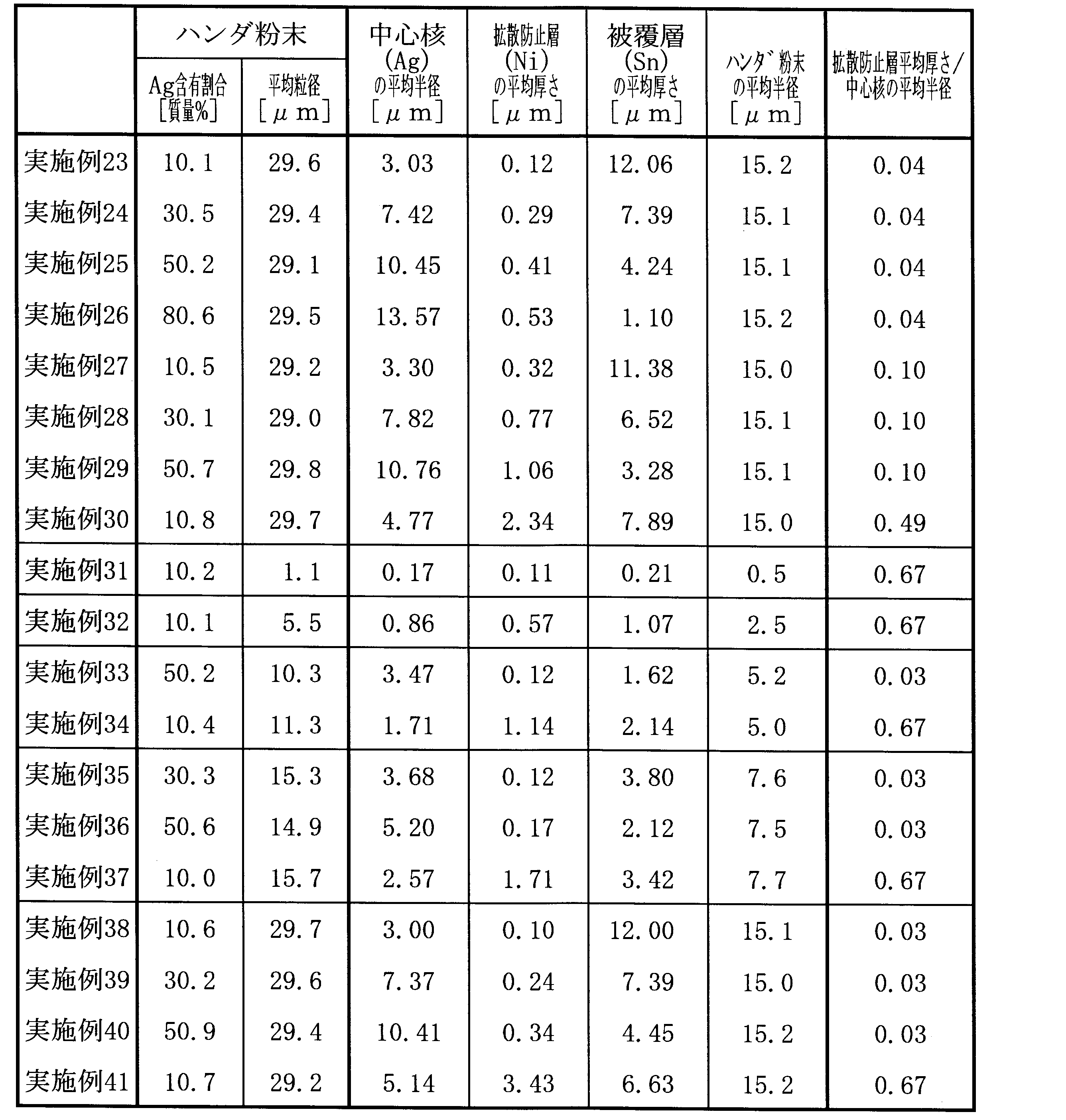

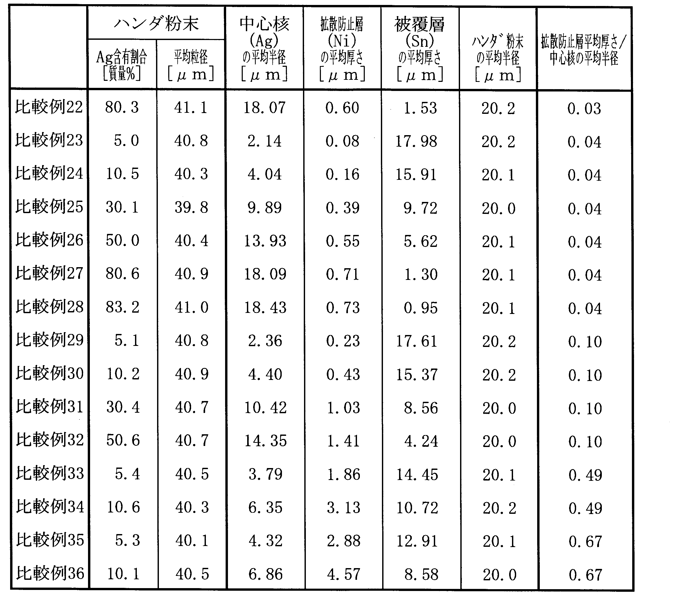
(1) ハンダ粉末の銀の含有割合の分析:誘導結合プラズマ発光分光分析(島津製作所社製 ICP発光分析装置:ICPS-7510)により、ハンダ粉末の銀の含有割合の分析を行った。
(2) ハンダ粉末の平均粒径:レーザー回折散乱法を用いた粒度分布測定装置(堀場製作所社製、レーザー回折/散乱式粒子径分布測定装置LA-950)にて粒径分布を測定し、その体積累積中位径(Median径、D50)をハンダ粉末の平均粒径とした。
(3) 銀からなる中心核の半径、ニッケルからなる拡散防止層の厚さ及び錫からなる被覆層の厚さの測定:ハンダ粉末を熱硬化性エポキシ樹脂に埋め込み、ハンダ粉末の断面を乾式研磨した後、電子顕微鏡(Scanning Electron Microscope、SEM)を用いて観察し、ハンダ粉末30個について、各々銀からなる中心核の半径、ニッケルからなる拡散防止層の厚さ及び錫からなる被覆層の厚さを測定し、各々の平均値を求めた。更に、上記測定から得られたニッケルからなる拡散防止層の厚さ及び銀からなる中心核の半径より厚さの平均値の比率(拡散防止層厚さ/中心核の半径)を算出した。
(4) 接合強度:溶剤として50質量%のジエチレングリコールモノヘキシルエーテルと、ロジンとして46質量%の重合ロジン(軟化点95℃)と、活性剤としてシクロヘキシルアミン臭化水素酸塩1.0質量%と、チキソ剤として硬化ひまし油3.0質量%とを混合してフラックスを調製した。次に、このフラックスと、実施例1~25及び比較例1~12で得られたハンダ粉末とを、フラックスを88質量%、ハンダ粉末を12質量%の割合で混合してハンダ用ペーストをそれぞれ調製した。
上記調製したペーストをピン転写法にて先端部の直径100μmのピンを用いて0.5mm厚のコバール(Fe-Ni-Co系合金)基板の所定位置に転写した。なお、コバール基板上にはNiメッキ、更にその上にAuフラッシュメッキを行った。続いて、転写されたペースト上に0.9mm□のLEDチップを搭載した。更に、加圧用治具を用いて、LEDチップ及び基板とを1.0MPaの圧力で加圧しながら、赤外線加熱炉にて窒素雰囲気中、0.17時間、所定の最大保持温度でリフローし、LEDチップとコバール基板とを接合させることにより、接合サンプルを得た。なお、上記リフロー時の最大保持温度を250℃、300℃、350℃の異なる温度に設定し、実施例又は比較例ごとにそれぞれ3つずつ接合サンプルを得た。
上記接合したコバール基板及びLEDチップとの接合強度について、JIS Z 3198-7に記されている鉛フリーハンダ試験方法-第7部の「チップ部品におけるハンダ接合のシェア強度測定方法」に準拠して、室温及び300℃で0日及び30日保管後の条件下で接合シェア強度をそれぞれ測定し、室温におけるシェア強度を100としたときの300℃での0日及び30日保管後の相対的シェア強度を求めた。表中、「優」は、相対的シェア強度が90以上であった場合を示し、「良」は、90未満から80以上であった場合を示し、「可」は、80未満から70以上であった場合を示し、「不可」は、70未満であった場合を示す。
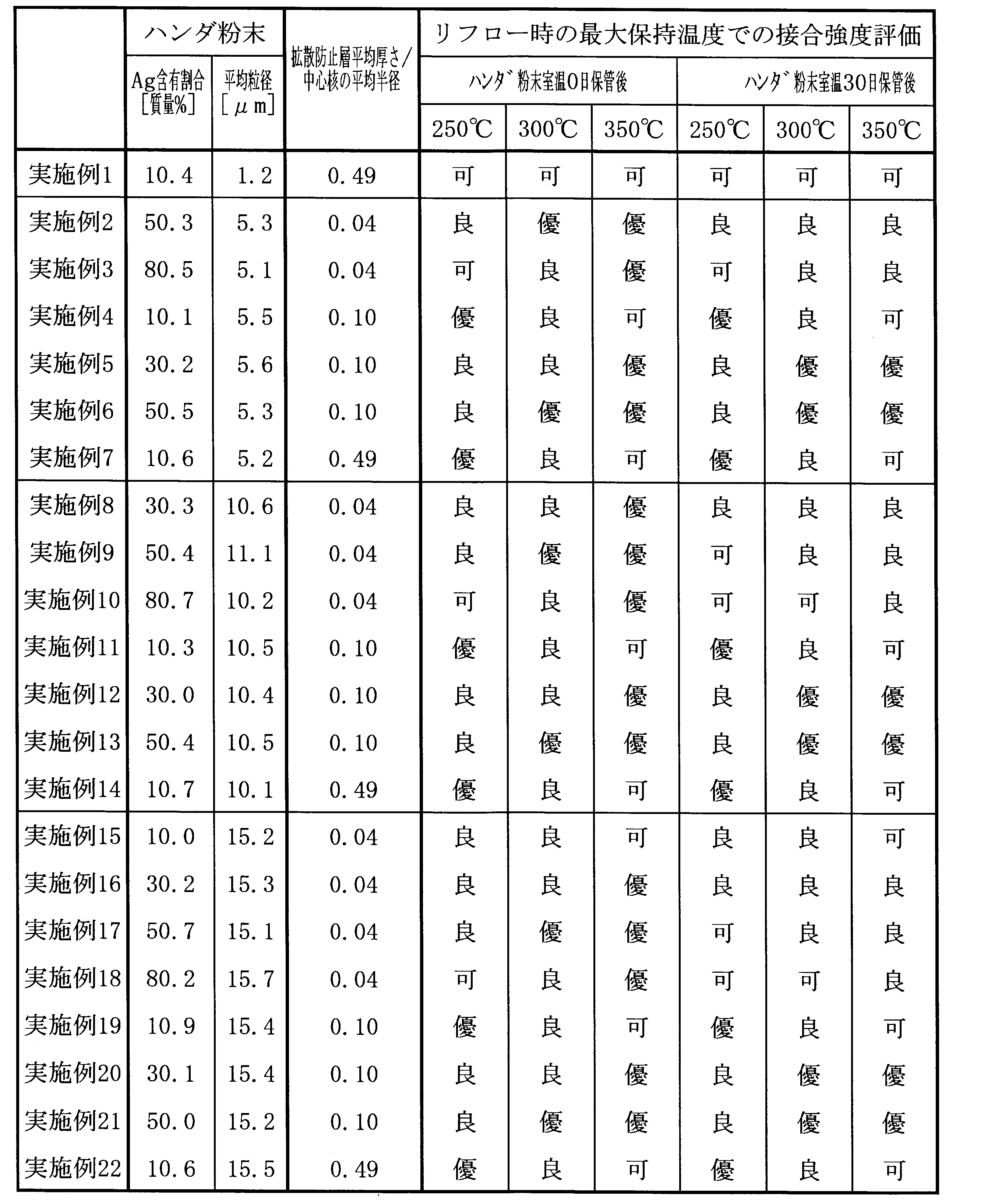
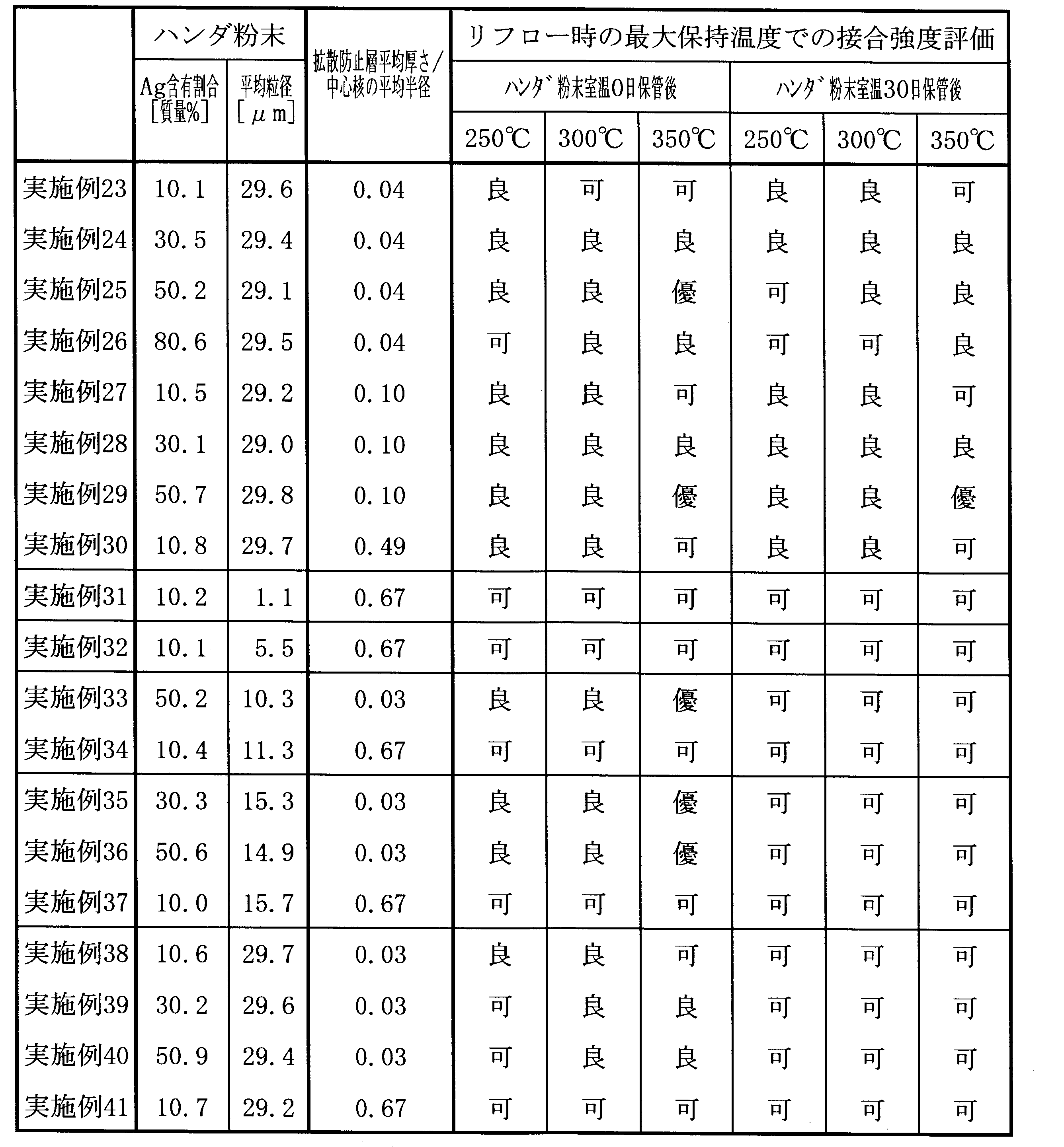
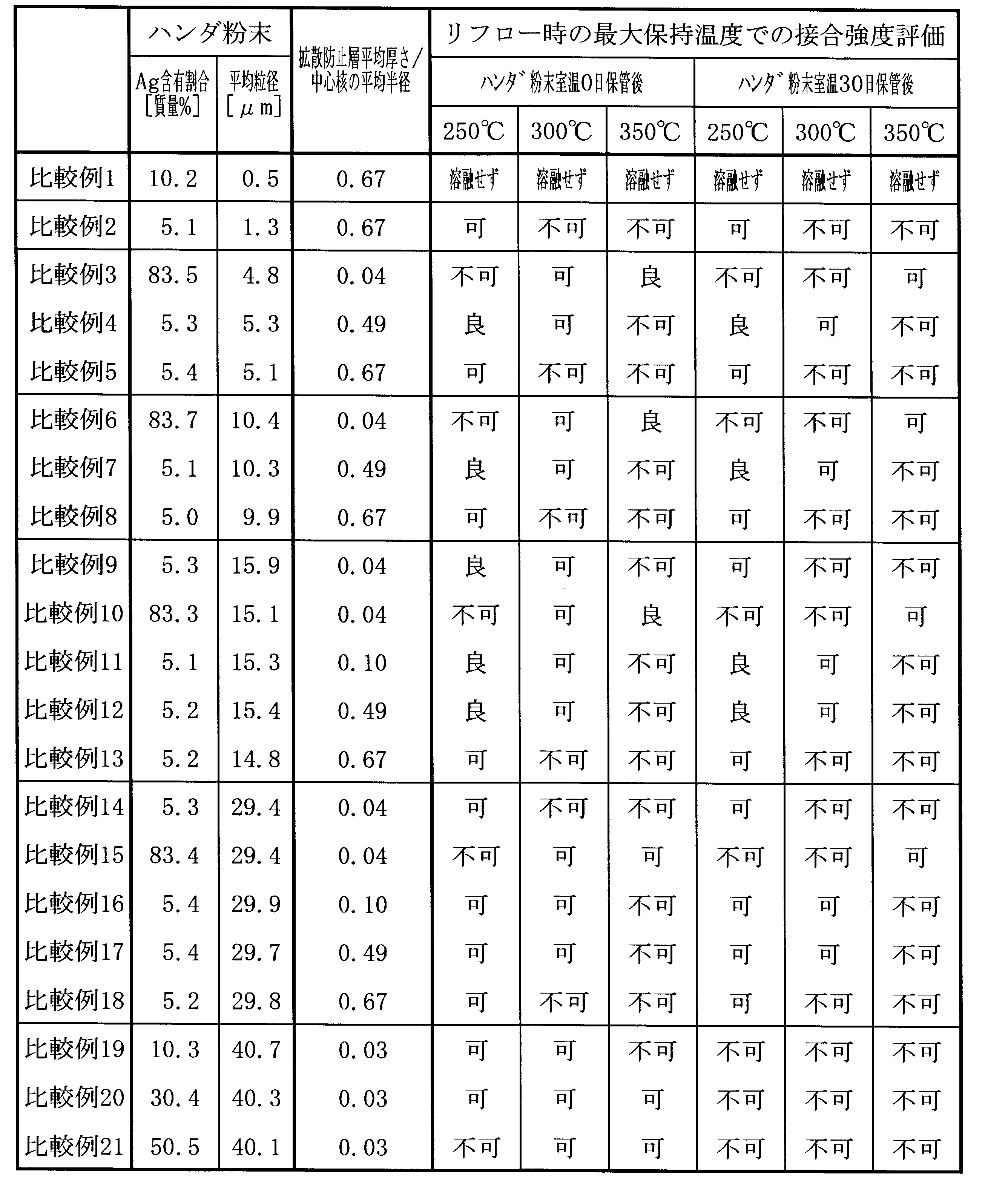

表5~表8から実施例1~41と比較例1~36とを比較すると次のことが分かった。
比較例1では、ハンダ粉末の平均粒径が0.5μmと小さすぎ、粉末表面の酸化膜の影響で、ハンダ粉末を保管する前から、ハンダ粉末が溶融しなかった。比較例2、4、5、7~9、11~14、16~18、23、29、33、35では、銀の含有量が5質量%程度で少なすぎ、凝固開始温度が低くなり、十分な耐熱性が得られなかったため、ハンダ粉末を保管前及び30日保管後の各350℃のリフロー温度では接合強度が不可であった。比較例3、6、10、15、28では、銀の含有量が83質量%程度で多すぎ、凝固開始温度が高くなりすぎ、ハンダ粉末を保管前及び30日保管後の250℃のリフロー時並びに30日保管後の300℃のリフロー時にハンダが溶融せず、接合強度が不可であった。比較例19~36では、ハンダ粉末の平均粒径が40μm程度で大きすぎ、リフロー後において大きなボイド(空孔)を有した接合層となり緻密な接合層が得られなかった。このためハンダ粉末を保管前及び30日保管後の250℃、300℃、350℃のいずれかのリフロー温度で接合強度が不可であった。
これに対して、ハンダ粉末の平均粒径が1μm以上30μm以下の範囲内にあり、ハンダ粉末の全体量100質量%に対し、銀の含有割合が10質量%以上81質量%以下の範囲内にある実施例1~41では、ハンダ粉末を保管前及び30日保管後の各250℃、300℃、350℃のすべてのリフロー温度において接合強度が可、良又は優であった。
本発明は、長期間保管することがあるハンダ粉末に好適に利用できる。また電子部品の実装、特に高温雰囲気に晒される電子部品の実装に好適に利用できる。
Claims (4)
- 中心核と前記中心核を被覆する被覆層で構成され、前記中心核が銀からなり、前記被覆層が錫からなるハンダ粉末において、
前記中心核と前記被覆層の間にニッケルからなる拡散防止層が形成され、
前記ハンダ粉末の平均粒径が1μm以上30μm以下であり、
前記ハンダ粉末の全体量100質量%に対し、銀の含有割合が10質量%以上81質量%以下である
ことを特徴とするハンダ粉末。 - 前記ニッケルからなる拡散防止層の厚さが前記中心核の半径を1とするときに0.04以上0.50以下の比率である請求項1記載のハンダ粉末。
- 請求項1又は2記載のハンダ粉末とハンダ用フラックスを混合してペースト化することによりハンダ用ペーストを調製する方法。
- 請求項3記載の方法により調製されたハンダ用ペーストを用いて電子部品を実装する方法。
Priority Applications (2)
| Application Number | Priority Date | Filing Date | Title |
|---|---|---|---|
| CN201680077136.XA CN108430689B (zh) | 2015-12-01 | 2016-11-29 | 焊料粉末及使用该粉末的焊接用浆料的制备方法 |
| KR1020187018393A KR102180860B1 (ko) | 2015-12-01 | 2016-11-29 | 솔더 분말 및 이 분말을 사용한 솔더용 페이스트의 조제 방법 |
Applications Claiming Priority (2)
| Application Number | Priority Date | Filing Date | Title |
|---|---|---|---|
| JP2015234641A JP6607006B2 (ja) | 2015-12-01 | 2015-12-01 | ハンダ粉末及びこの粉末を用いたハンダ用ペーストの調製方法 |
| JP2015-234641 | 2015-12-01 |
Publications (1)
| Publication Number | Publication Date |
|---|---|
| WO2017094713A1 true WO2017094713A1 (ja) | 2017-06-08 |
Family
ID=58796882
Family Applications (1)
| Application Number | Title | Priority Date | Filing Date |
|---|---|---|---|
| PCT/JP2016/085389 Ceased WO2017094713A1 (ja) | 2015-12-01 | 2016-11-29 | ハンダ粉末及びこの粉末を用いたハンダ用ペーストの調製方法 |
Country Status (5)
| Country | Link |
|---|---|
| JP (1) | JP6607006B2 (ja) |
| KR (1) | KR102180860B1 (ja) |
| CN (1) | CN108430689B (ja) |
| TW (1) | TWI670136B (ja) |
| WO (1) | WO2017094713A1 (ja) |
Cited By (1)
| Publication number | Priority date | Publication date | Assignee | Title |
|---|---|---|---|---|
| JP2020112487A (ja) * | 2019-01-15 | 2020-07-27 | 株式会社日本マイクロニクス | プローブ基板及び電気的接続装置 |
Families Citing this family (3)
| Publication number | Priority date | Publication date | Assignee | Title |
|---|---|---|---|---|
| KR20220032918A (ko) | 2020-09-08 | 2022-03-15 | 삼성전자주식회사 | 하이브리드 접합 구조물 및 이를 포함한 반도체 소자 |
| KR102912595B1 (ko) | 2020-09-23 | 2026-01-13 | 삼성전자주식회사 | 하이브리드 접합 구조물, 이를 포함한 반도체 소자, 및 반도체 소자 제조방법 |
| CN113751922A (zh) * | 2021-10-11 | 2021-12-07 | 中国科学院电工研究所 | 一种无铅焊料及其制备方法和应用 |
Citations (4)
| Publication number | Priority date | Publication date | Assignee | Title |
|---|---|---|---|---|
| JPH02179385A (ja) * | 1988-12-29 | 1990-07-12 | Tokuriki Honten Co Ltd | 低融点Agはんだ |
| JP2010099736A (ja) * | 2008-09-25 | 2010-05-06 | Hitachi Metals Ltd | 耐落下衝撃特性に優れた接続端子用ボールおよび接続端子ならびに電子部品 |
| JP2012157870A (ja) * | 2011-01-31 | 2012-08-23 | Mitsubishi Materials Corp | ハンダ粉末及びこの粉末を用いたハンダ用ペースト |
| JP2014193474A (ja) * | 2013-03-29 | 2014-10-09 | Mitsubishi Materials Corp | ハンダ粉末及びこの粉末を用いたハンダ用ペースト |
Family Cites Families (12)
| Publication number | Priority date | Publication date | Assignee | Title |
|---|---|---|---|---|
| TWI248842B (en) * | 2000-06-12 | 2006-02-11 | Hitachi Ltd | Semiconductor device and semiconductor module |
| US6892925B2 (en) * | 2002-09-18 | 2005-05-17 | International Business Machines Corporation | Solder hierarchy for lead free solder joint |
| US7265046B2 (en) * | 2002-09-27 | 2007-09-04 | Neomax Material Co., Ltd. | Method of making a solder ball |
| US7524351B2 (en) * | 2004-09-30 | 2009-04-28 | Intel Corporation | Nano-sized metals and alloys, and methods of assembling packages containing same |
| JP5042017B2 (ja) * | 2005-05-27 | 2012-10-03 | 株式会社Neomaxマテリアル | 銀被覆ボールおよびその製造方法 |
| US7758916B2 (en) * | 2006-11-13 | 2010-07-20 | Sulzer Metco (Us), Inc. | Material and method of manufacture of a solder joint with high thermal conductivity and high electrical conductivity |
| JP2008138266A (ja) | 2006-12-04 | 2008-06-19 | Mitsubishi Materials Corp | ハンダ粉末及び該粉末を用いたハンダ用ペースト |
| JP2012076086A (ja) * | 2010-09-30 | 2012-04-19 | Mitsubishi Materials Corp | ハンダ粉末及びこの粉末を用いたハンダ用ペースト |
| JP2012115860A (ja) * | 2010-11-30 | 2012-06-21 | Mitsubishi Materials Corp | ハンダ粉末の製造方法及び該方法により得られたハンダ粉末 |
| KR101451559B1 (ko) * | 2011-09-02 | 2014-10-15 | 미쓰비시 마테리알 가부시키가이샤 | 땜납 분말 및 이 분말을 사용한 땜납용 페이스트 |
| KR101858884B1 (ko) * | 2013-11-05 | 2018-05-16 | 센주긴조쿠고교 가부시키가이샤 | Cu 핵 볼, 땜납 페이스트, 폼 땜납 및 납땜 조인트 |
| JP5652560B1 (ja) * | 2014-02-04 | 2015-01-14 | 千住金属工業株式会社 | Cu核ボール、はんだペースト、フォームはんだ及びはんだ継手 |
-
2015
- 2015-12-01 JP JP2015234641A patent/JP6607006B2/ja not_active Expired - Fee Related
-
2016
- 2016-11-29 WO PCT/JP2016/085389 patent/WO2017094713A1/ja not_active Ceased
- 2016-11-29 KR KR1020187018393A patent/KR102180860B1/ko not_active Expired - Fee Related
- 2016-11-29 CN CN201680077136.XA patent/CN108430689B/zh not_active Expired - Fee Related
- 2016-11-30 TW TW105139489A patent/TWI670136B/zh not_active IP Right Cessation
Patent Citations (4)
| Publication number | Priority date | Publication date | Assignee | Title |
|---|---|---|---|---|
| JPH02179385A (ja) * | 1988-12-29 | 1990-07-12 | Tokuriki Honten Co Ltd | 低融点Agはんだ |
| JP2010099736A (ja) * | 2008-09-25 | 2010-05-06 | Hitachi Metals Ltd | 耐落下衝撃特性に優れた接続端子用ボールおよび接続端子ならびに電子部品 |
| JP2012157870A (ja) * | 2011-01-31 | 2012-08-23 | Mitsubishi Materials Corp | ハンダ粉末及びこの粉末を用いたハンダ用ペースト |
| JP2014193474A (ja) * | 2013-03-29 | 2014-10-09 | Mitsubishi Materials Corp | ハンダ粉末及びこの粉末を用いたハンダ用ペースト |
Cited By (1)
| Publication number | Priority date | Publication date | Assignee | Title |
|---|---|---|---|---|
| JP2020112487A (ja) * | 2019-01-15 | 2020-07-27 | 株式会社日本マイクロニクス | プローブ基板及び電気的接続装置 |
Also Published As
| Publication number | Publication date |
|---|---|
| JP6607006B2 (ja) | 2019-11-20 |
| CN108430689A (zh) | 2018-08-21 |
| KR20180088440A (ko) | 2018-08-03 |
| JP2017100156A (ja) | 2017-06-08 |
| TWI670136B (zh) | 2019-09-01 |
| TW201739560A (zh) | 2017-11-16 |
| KR102180860B1 (ko) | 2020-11-19 |
| CN108430689B (zh) | 2021-10-15 |
Similar Documents
| Publication | Publication Date | Title |
|---|---|---|
| JP6587099B2 (ja) | ハンダ粉末及びその製造方法並びにこの粉末を用いたハンダ用ペーストの調製方法 | |
| JP6079374B2 (ja) | ハンダ粉末の製造方法及びこの粉末を用いたハンダ用ペースト | |
| JP6428407B2 (ja) | ハンダ粉末の製造方法及びこの粉末を用いたハンダ用ペーストの製造方法 | |
| JP6079375B2 (ja) | ハンダ粉末及びその製造方法並びにこの粉末を用いたハンダ用ペースト | |
| JP6607006B2 (ja) | ハンダ粉末及びこの粉末を用いたハンダ用ペーストの調製方法 | |
| JP6428408B2 (ja) | ハンダ粉末の製造方法及びこの粉末を用いたハンダ用ペーストの製造方法 | |
| JP6720515B2 (ja) | Au−Snはんだ粉末及びこの粉末を含むはんだ用ペースト | |
| JP6645317B2 (ja) | 接合用粉末及びこの粉末の製造方法並びにこの粉末を用いた接合用ペーストの製造方法 | |
| JP6428409B2 (ja) | ハンダ粉末及びこの粉末を用いたハンダ用ペースト | |
| JP2018135568A (ja) | 接合用粉末及びその製造方法 | |
| JP6645318B2 (ja) | 接合用粉末及びこの粉末の製造方法並びにこの粉末を用いた接合用ペーストの製造方法 | |
| JP6507970B2 (ja) | Au系はんだ粉末及びこの粉末を含むはんだ用ペースト | |
| JP2018135553A (ja) | 接合用粉末及びその製造方法 |
Legal Events
| Date | Code | Title | Description |
|---|---|---|---|
| 121 | Ep: the epo has been informed by wipo that ep was designated in this application |
Ref document number: 16870650 Country of ref document: EP Kind code of ref document: A1 |
|
| NENP | Non-entry into the national phase |
Ref country code: DE |
|
| ENP | Entry into the national phase |
Ref document number: 20187018393 Country of ref document: KR Kind code of ref document: A |
|
| 122 | Ep: pct application non-entry in european phase |
Ref document number: 16870650 Country of ref document: EP Kind code of ref document: A1 |